US9799660B1 - Stable and reliable FinFET SRAM with improved beta ratio - Google Patents
Stable and reliable FinFET SRAM with improved beta ratio Download PDFInfo
- Publication number
- US9799660B1 US9799660B1 US15/151,622 US201615151622A US9799660B1 US 9799660 B1 US9799660 B1 US 9799660B1 US 201615151622 A US201615151622 A US 201615151622A US 9799660 B1 US9799660 B1 US 9799660B1
- Authority
- US
- United States
- Prior art keywords
- pass
- gate
- mask layer
- fin
- gate transistor
- Prior art date
- Legal status (The legal status is an assumption and is not a legal conclusion. Google has not performed a legal analysis and makes no representation as to the accuracy of the status listed.)
- Expired - Fee Related
Links
Images


Classifications
-
- H—ELECTRICITY
- H10—SEMICONDUCTOR DEVICES; ELECTRIC SOLID-STATE DEVICES NOT OTHERWISE PROVIDED FOR
- H10B—ELECTRONIC MEMORY DEVICES
- H10B10/00—Static random access memory [SRAM] devices
- H10B10/12—Static random access memory [SRAM] devices comprising a MOSFET load element
-
- H01L27/1104—
-
- H—ELECTRICITY
- H01—ELECTRIC ELEMENTS
- H01L—SEMICONDUCTOR DEVICES NOT COVERED BY CLASS H10
- H01L21/00—Processes or apparatus adapted for the manufacture or treatment of semiconductor or solid state devices or of parts thereof
- H01L21/02—Manufacture or treatment of semiconductor devices or of parts thereof
- H01L21/04—Manufacture or treatment of semiconductor devices or of parts thereof the devices having at least one potential-jump barrier or surface barrier, e.g. PN junction, depletion layer or carrier concentration layer
- H01L21/18—Manufacture or treatment of semiconductor devices or of parts thereof the devices having at least one potential-jump barrier or surface barrier, e.g. PN junction, depletion layer or carrier concentration layer the devices having semiconductor bodies comprising elements of Group IV of the Periodic System or AIIIBV compounds with or without impurities, e.g. doping materials
- H01L21/30—Treatment of semiconductor bodies using processes or apparatus not provided for in groups H01L21/20 - H01L21/26
- H01L21/302—Treatment of semiconductor bodies using processes or apparatus not provided for in groups H01L21/20 - H01L21/26 to change their surface-physical characteristics or shape, e.g. etching, polishing, cutting
- H01L21/306—Chemical or electrical treatment, e.g. electrolytic etching
- H01L21/3065—Plasma etching; Reactive-ion etching
-
- H—ELECTRICITY
- H01—ELECTRIC ELEMENTS
- H01L—SEMICONDUCTOR DEVICES NOT COVERED BY CLASS H10
- H01L21/00—Processes or apparatus adapted for the manufacture or treatment of semiconductor or solid state devices or of parts thereof
- H01L21/02—Manufacture or treatment of semiconductor devices or of parts thereof
- H01L21/04—Manufacture or treatment of semiconductor devices or of parts thereof the devices having at least one potential-jump barrier or surface barrier, e.g. PN junction, depletion layer or carrier concentration layer
- H01L21/18—Manufacture or treatment of semiconductor devices or of parts thereof the devices having at least one potential-jump barrier or surface barrier, e.g. PN junction, depletion layer or carrier concentration layer the devices having semiconductor bodies comprising elements of Group IV of the Periodic System or AIIIBV compounds with or without impurities, e.g. doping materials
- H01L21/30—Treatment of semiconductor bodies using processes or apparatus not provided for in groups H01L21/20 - H01L21/26
- H01L21/302—Treatment of semiconductor bodies using processes or apparatus not provided for in groups H01L21/20 - H01L21/26 to change their surface-physical characteristics or shape, e.g. etching, polishing, cutting
- H01L21/306—Chemical or electrical treatment, e.g. electrolytic etching
- H01L21/308—Chemical or electrical treatment, e.g. electrolytic etching using masks
- H01L21/3083—Chemical or electrical treatment, e.g. electrolytic etching using masks characterised by their size, orientation, disposition, behaviour, shape, in horizontal or vertical plane
- H01L21/3085—Chemical or electrical treatment, e.g. electrolytic etching using masks characterised by their size, orientation, disposition, behaviour, shape, in horizontal or vertical plane characterised by their behaviour during the process, e.g. soluble masks, redeposited masks
-
- H—ELECTRICITY
- H01—ELECTRIC ELEMENTS
- H01L—SEMICONDUCTOR DEVICES NOT COVERED BY CLASS H10
- H01L21/00—Processes or apparatus adapted for the manufacture or treatment of semiconductor or solid state devices or of parts thereof
- H01L21/02—Manufacture or treatment of semiconductor devices or of parts thereof
- H01L21/04—Manufacture or treatment of semiconductor devices or of parts thereof the devices having at least one potential-jump barrier or surface barrier, e.g. PN junction, depletion layer or carrier concentration layer
- H01L21/50—Assembly of semiconductor devices using processes or apparatus not provided for in a single one of the subgroups H01L21/06 - H01L21/326, e.g. sealing of a cap to a base of a container
- H01L21/56—Encapsulations, e.g. encapsulation layers, coatings
-
- H—ELECTRICITY
- H01—ELECTRIC ELEMENTS
- H01L—SEMICONDUCTOR DEVICES NOT COVERED BY CLASS H10
- H01L21/00—Processes or apparatus adapted for the manufacture or treatment of semiconductor or solid state devices or of parts thereof
- H01L21/70—Manufacture or treatment of devices consisting of a plurality of solid state components formed in or on a common substrate or of parts thereof; Manufacture of integrated circuit devices or of parts thereof
- H01L21/77—Manufacture or treatment of devices consisting of a plurality of solid state components or integrated circuits formed in, or on, a common substrate
- H01L21/78—Manufacture or treatment of devices consisting of a plurality of solid state components or integrated circuits formed in, or on, a common substrate with subsequent division of the substrate into plural individual devices
- H01L21/82—Manufacture or treatment of devices consisting of a plurality of solid state components or integrated circuits formed in, or on, a common substrate with subsequent division of the substrate into plural individual devices to produce devices, e.g. integrated circuits, each consisting of a plurality of components
- H01L21/822—Manufacture or treatment of devices consisting of a plurality of solid state components or integrated circuits formed in, or on, a common substrate with subsequent division of the substrate into plural individual devices to produce devices, e.g. integrated circuits, each consisting of a plurality of components the substrate being a semiconductor, using silicon technology
- H01L21/8232—Field-effect technology
- H01L21/8234—MIS technology, i.e. integration processes of field effect transistors of the conductor-insulator-semiconductor type
- H01L21/823431—MIS technology, i.e. integration processes of field effect transistors of the conductor-insulator-semiconductor type with a particular manufacturing method of transistors with a horizontal current flow in a vertical sidewall of a semiconductor body, e.g. FinFET, MuGFET
-
- H—ELECTRICITY
- H01—ELECTRIC ELEMENTS
- H01L—SEMICONDUCTOR DEVICES NOT COVERED BY CLASS H10
- H01L23/00—Details of semiconductor or other solid state devices
- H01L23/28—Encapsulations, e.g. encapsulating layers, coatings, e.g. for protection
- H01L23/31—Encapsulations, e.g. encapsulating layers, coatings, e.g. for protection characterised by the arrangement or shape
- H01L23/3157—Partial encapsulation or coating
- H01L23/3171—Partial encapsulation or coating the coating being directly applied to the semiconductor body, e.g. passivation layer
-
- H—ELECTRICITY
- H01—ELECTRIC ELEMENTS
- H01L—SEMICONDUCTOR DEVICES NOT COVERED BY CLASS H10
- H01L27/00—Devices consisting of a plurality of semiconductor or other solid-state components formed in or on a common substrate
- H01L27/02—Devices consisting of a plurality of semiconductor or other solid-state components formed in or on a common substrate including semiconductor components specially adapted for rectifying, oscillating, amplifying or switching and having at least one potential-jump barrier or surface barrier; including integrated passive circuit elements with at least one potential-jump barrier or surface barrier
- H01L27/0203—Particular design considerations for integrated circuits
- H01L27/0207—Geometrical layout of the components, e.g. computer aided design; custom LSI, semi-custom LSI, standard cell technique
Definitions
- the present invention relates to a semiconductor memory device and to a method of fabricating a semiconductor memory device, and more particularly, to a static random access memory (SRAM) device with an improved beta ratio.
- SRAM static random access memory
- SRAM devices are generally used in applications requiring high speed, such as, memory in a data processing system, and typically consist of six transistors (6T): two P channel field effect transistors (PFETs) for a pull-up operation, two N channel field effect transistors (NFETs) for pull down, and two NFETs for input/output (i.e. passgate) access.
- 6T six transistors
- PFETs P channel field effect transistors
- NFETs N channel field effect transistors
- passgate input/output
- the stability of a 6T SRAM cell is defined by a beta ratio which, for instance, is the ratio of the drive currents of the pull-down transistors to the drive currents of the respective pass-gate transistors.
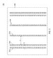
- FIG. 1 illustrates a top plan view of a typical 6T SRAM device 100 .
- the SRAM device 100 typically includes one or more regions, for instance, region A and region B.
- regions A and B include, for instance, two pass-gate transistors 112 that are electrically coupled to two pull-down transistors 110 which, in turn, are electrically coupled to two pull-up transistors 108 , respectively.
- each of the two pass-gate transistors 112 include two fin structures (referred to hereinafter as “fins”) that allow electrically coupling of one pass-gate transistor 112 to an adjacent pass-gate transistor 112 . Additionally, the two fins of the pass-gate transistors 112 also enable electrical coupling of the pass-gate transistor to the neighboring pull-down transistors 110 , respectively. Although not depicted in the figures, one skilled in the art will understand that, a source region and a drain region are formed at opposite ends of each of the pass-gate FinFETs 112 , pull-down FinFETs 110 and pull-up FinFETs 108 .
- an equal number of pull-down devices and pass-gate devices provide a tradeoff between the cell size and the cell speed.
- the beta ratio is equal to 1.
- the unitary beta ratio could lead to undesirable issues such as, access disturb.
- higher beta ratios are desirable to improve the stability of the SRAM cell, without increasing the overall size of the SRAM cell.
- regions, for instance, regions A and B are expanded to form bigger cells which, for instance, are more stable because bigger FET features are relatively more precise.
- a method for forming a semiconductor memory device which includes, for instance, providing at least two mask layers over a pair of fin structures extended above a substrate, wherein a first mask layer of the at least two mask layers is orthogonal to a second mask layer of the at least two mask layers; and patterning the pair of fin structures to define a pass-gate transistor, wherein the first mask layer facilitates removing of a portion of a first fin structure of the pair of fin structures to define a first pass-gate fin portion of the pass-gate transistor, and the second mask layer protects a second fin structure of the pair of fin structures to define a second pass-gate fin portion of the pass-gate transistor.
- a semiconductor memory device which includes, for instance, a static random-access memory (SRAM) cell including at least one pass-gate transistor and at least one pull-down transistor, wherein each of the at least one pass-gate transistor and the at least one pull-down transistor have a pair of fin structures extended above a substrate, and electrically coupled to each other, wherein a fin structure of the pair of fin structures is encapsulated within a gate structure of the at least one pass-gate transistor.
- SRAM static random-access memory
- a method for forming a semiconductor memory device which includes, for instance, providing at least two mask layers over a pair of fin structures extended above a substrate, a first mask layer of the at least two mask layers being orthogonal to a second mask layer of the at least two mask layers, where the first mask layer of the at least two mask layers facilitates modulating stability of the semiconductor memory device, without affecting the second mask layer of the at least two mask layers.
- FIG. 1 depicts a plan view of one embodiment of a conventional SRAM device
- FIG. 2 depicts a plan view of one embodiment of a structure obtained during static random-access memory (SRAM) fabrication process, and illustrates one or more fins disposed over the substrate, in accordance with one or more aspects of the present invention
- FIG. 3 is a plan view of the structure of FIG. 2 with one or more first lithographic mask layer(s) having been disposed over the fin(s), in accordance with one or more aspects of the present invention
- FIG. 4 is a plan view of the structure of FIG. 3 with one or more cut mask layer(s) having been disposed orthogonal to the first lithographic mask layer(s) over the fin(s), in accordance with one or more aspects of the present invention
- FIG. 5 is a plan view of the structure of FIG. 4 after providing one or more second lithographic mask layer(s) orthogonal to the cut mask layer(s) over the fin(s), in accordance with one or more aspects of the present invention
- FIG. 6 is a plan view of the structure of FIG. 5 after patterning the fin(s), for instance, using the cut mask layer(s), to define a pass-gate transistor, in accordance with one or more aspects of the present invention
- FIG. 7 is a plan view of the structure of FIG. 6 with gate structure(s) having been provided over the patterned fin(s), in accordance with one or more aspects of the present invention
- FIG. 8 is a plan view of a resultant structure of FIG. 7 after expanding the structure during the SRAM fabrication process, in accordance with one or more aspects of the present invention.
- FIG. 9 is a plan view of an alternate embodiment of a resultant structure of FIG. 5 with the stability of the semiconductor memory device having been modulated, in accordance with one or more aspects of the present invention.
- the present invention provides, inter alia, a fabrication method and a structure for a SRAM device with improved beta ratio.
- a fabrication method and a structure for a SRAM device with improved beta ratio As described above, and in one aspect, during conventional FinFET fabrication processing, and in particular, during SRAM fabrication processing, one or more fin structures or fins residing over a substrate may be spaced apart, and during bulk FinFET or SRAM fabrication processing, more fins may have been created than required for a particular circuit or device.
- a fin cut or fin removal process is employed to remove one or more unwanted fin structures, in particular, at the pass-gate transistor of the SRAM device. Such removal of an unwanted fin and subsequent tucking of the unwanted fin within an overlying gate structure at the pass-gate transistor, for instance, could improve the beta ratio of a SRAM device.
- the conventional processing techniques employed could lead to inadvertently removing the adjacent fin along with the unwanted fin, thereby resulting in performance degradation of the resultant SRAM device.
- the conventional processing techniques employed during the fin cut processing could, for instance, involve utilizing a pair of mask layers (e.g., lithographic mask layer and cut mask layer) to pattern the various cells of the SRAM device.
- the cut mask layer is conventionally employed to cut the pull-up fin.
- the cut mask layer has been utilized to cut both the pull-up fin and the pass-gate fin, while in the technology nodes below 14 nm, the cut mask layer has been utilized to cut the pull-up fin, resulting in constraining the beta ratio of the SRAM device to be 1. Still further, the conventional processing techniques employed during the fin cut processing could, disadvantageously, result in rounding of a remaining fin portion. This rounding profile of the remaining fin portion may cause subsequent epitaxial growth problems at the source region and the drain region of the pass-gate transistor, and for at least this reasoning is undesirable.
- a method for forming a semiconductor memory device which includes, for instance, providing at least two mask layers over a pair of fin structures extended above a substrate, wherein a first mask layer of the at least two mask layers is orthogonal to a second mask layer of the at least two mask layers; and patterning the pair of fin structures to define a pass-gate transistor, wherein the first mask layer facilitates removing of a portion of a first fin structure of the pair of fin structures to define a first pass-gate fin portion of the pass-gate transistor, and the second mask layer protects a second fin structure of the pair of fin structures to define a second pass-gate fin portion of the pass-gate transistor.
- the patterning of the pair of fin structures with the first mask layer and the second mask layer provides the first pass-gate fin portion of the pass-gate transistor with squared edges.
- the fabrication method may include a gate structure extending at least partially over the pair of fin structures of the pass-gate transistor, and the first pass-gate fin portion of the pass-gate transistor is encapsulated within the gate structure, selective to the second pass-gate fin portion. Such encapsulation of the first pass-gate fin portion within the gate structure of the pass-gate transistor enhances a beta ratio of the semiconductor memory device.
- the first mask layer may include a first lithographic mask layer and a cut mask layer, with the first lithographic mask layer being orthogonal to the cut mask layer.
- the cut mask layer facilitates removing of the portion of the first fin structure.
- the patterning of the pair of fin structures may include modifying the selective removal of the portion of the first fin structure with the cut mask layer to provide the first pass-gate fin portion with squared edges so as to facilitate encapsulation of the first pass-gate fin portion within the gate structure.
- the second mask layer may include a second lithographic mask layer, with the second mask layer being spaced parallel to the first lithographic mask layer. In such an implementation, the second mask layer and the first lithographic mask layer define the second fin portion of the pass-gate transistor.
- the fabrication method may include an additional first lithographic mask layer, with the additional first lithographic mask layer being spaced parallel to the first lithographic mask layer.
- the additional first lithographic mask layer defines a pull-up transistor, and the pull-up transistor is electrically coupled with the pull-down transistor.
- the fabrication method may include an additional pass-gate transistor, with the additional pass-gate transistor including a first pass-gate fin portion and a second pass-gate fin portion, and the additional pass-gate transistor is in-line with the pass-gate transistor, where the first pass-gate fin portion of the second pass-gate transistor is electrically isolated from the first pass-gate fin portion of the pass-gate transistor, and the second pass-gate fin portion of the second pass-gate transistor is electrically coupled with the second pass-gate fin portion of the pass-gate transistor.
- the electrical isolation of the first pass-gate fin portion of the pass-gate transistor and the first pass-gate fin portion of the additional pass-gate transistor enhances a beta ratio of the semiconductor memory device.
- the enhanced beta ratio of the semiconductor memory device may be about 2.0 or more.
- a semiconductor memory device which includes, for instance, a static random-access memory (SRAM) cell including at least one pass-gate transistor and at least one pull-down transistor, where each of the at least one pass-gate transistor and the at least one pull-down transistor have a pair of fin structures extended above a substrate, and electrically coupled to each other, where a fin structure of the pair of fin structures is encapsulated within a gate structure of the at least one pass-gate transistor.
- SRAM static random-access memory
- a method for forming a semiconductor memory device which includes, for instance, providing at least two mask layers over a pair of fin structures extended above a substrate, a first mask layer of the at least two mask layers being orthogonal to a second mask layer of the at least two mask layers, where the first mask layer of the at least two mask layers facilitates modulating stability of the semiconductor memory device, without affecting the second mask layer of the at least two mask layers.
- FIGS. 2-8 depict one embodiment of a method for forming a semiconductor memory device, for example, a SRAM device with an improved beta ratio, in accordance with one or more aspects of the present invention.
- the two or more mask layers employed in the patterning of the fins facilitates selectively removing a portion of the unwanted fin, leaving a patterned fin with squared edges which, for instance, are encapsulated within an overlying gate structure, thereby creating an electrical isolation therein, and improving the beta ratio of the resultant SRAM device.
- FIG. 2 depicts a plan view of one embodiment of a structure 200 obtained during static random-access memory (SRAM) fabrication process, in accordance with one or more aspects of the present invention.
- structure 200 includes a substrate 202 , which may be (in one example) a bulk semiconductor material such as, for example, a bulk silicon wafer.
- substrate 202 may be any silicon-containing substrate including, but not limited to, silicon (Si), single crystal silicon (Si), polycrystalline Si, amorphous Si or the like.
- Substrate structure 202 may in addition, or instead, include various isolations, dopings and/or device features.
- substrate structure 202 may include an insulating substrate layer which, for instance, may be, or include, a buried dielectric layer such as, for example, a buried oxide (BOX) layer, silicon-on-nothing (SON), silicon-on-insulator or the like.
- a buried oxide layer may be fabricated by employing SIMOX (Separation by Implanted Oxygen) technique which, for instance, may include implanting high doses of oxygen (O + ) ions into the silicon substrate, and annealing at a high temperature to form a layer of buried oxide over the silicon substrate.
- SIMOX Separatation by Implanted Oxygen
- the fabrication of the buried oxide layer may result in a residual layer of semiconductor material (not shown) which, for instance, may include a silicon material, being disposed over the insulating substrate layer (not shown).
- one or more fin structures or fins 204 may be formed extending from substrate 202 .
- fins 204 may be formed by patterning one or more portions of substrate 202 , thereby creating one or more fins 204 of the same semiconductor material as the substrate 202 , for example, silicon material.
- formation of fins 204 may be achieved by patterning the substrate 202 using any of various approaches including: direct lithography; sidewall image transfer technique; extreme ultraviolet technique (EUV); e-beam technique; litho-etch litho-etch or litho-freeze-litho-etch.
- EUV extreme ultraviolet technique
- EUV extreme ultraviolet technique
- e-beam technique litho-etch litho-etch or litho-freeze-litho-etch.
- the removal may be performed, for example, by any suitable etching process, such as, anisotropic dry etching processes, for instance, reactive-ion-etching (RIE) process.
- etching process such as, anisotropic dry etching processes, for instance, reactive-ion-etching (RIE) process.
- RIE reactive-ion-etching
- fins 204 may have any suitable height.
- the distance between two adjacent fins may also be varied depending upon the various process parameters employed. As illustrated, while two adjacent fins (for instance, fins 204 a and 204 b ) may be spaced closer (for instance, distance D 2 ), the distance between adjacent fins (for instance, fins 204 b and 204 c ) may also be varied by distance D 1 . As described further below, these variations in distances between the fins facilitates forming various pull-up transistors, pull-down transistors and pass-gate transistors of the SRAM device, during subsequent fabrication processing.
- the pair of fins 204 a and 204 b may be utilized to form one or more pull-down transistors and one or more pass-gate transistors, while the isolated fin 204 c may be utilized to form one or more pull-up transistors.
- FIG. 3 is a plan view of the structure of FIG. 2 with one or more first lithographic mask layer(s) 206 having been disposed over the fin(s) 204 , in accordance with one or more aspects of the present invention.
- the first lithographic mask layer(s) 206 which, for instance, may include, or be fabricated of a photoresist material or a photosensitive dielectric material, such as, photosensitive polyimide, and may be deposited using conventional deposition processes, such as, spin-on coating.
- This first lithographic mask layer 206 may be used, in part, to protect and/or preserve the smaller features of the fins 204 than can be protected using a conventional organic mask layer.
- the first lithographic mask layer 206 may be selectively disposed over fin 204 a of the pair of fins 204 a and 204 b , while the fin 204 b is exposed, thereby defining one fin of the pull-down fin region 208 , as well as one fin of the pass-gate fin region 214 , upon which the pull-down transistor and the pass-gate transistor can be fabricated respectively, during subsequent fabrication processing.
- one of the first lithographic mask layer(s) 206 is spaced parallel to another first lithographic mask layer 206 which, for instance, facilitates defining the pull-up fin region 210 , upon which the pull-up transistor of the SRAM device can be fabricated, during subsequent fabrication processing.
- FIG. 4 is a plan view of the structure of FIG. 3 with one or more cut mask layer(s) 212 having been disposed over the fin(s) 204 , in accordance with one or more aspects of the present invention.
- the cut mask layer(s) 212 are formed orthogonal to the first lithographic mask layer(s) 206 disposed over fins 204 at selected areas, thereby defining pass-gate fin portion 214 a and pass-gate fin portion 214 b of the one or more pass-gate fin regions 214 , upon which the pass-gate transistor could be formed, during the subsequent fabrication processing.
- the cut mask layer(s) 212 may include, or be fabricated of, a photoresist material or a photosensitive dielectric material such as, photosensitive polyimide and may be deposited using a variety of conventional deposition processes, such as, for example, spin-on coating or the like.
- the first lithographic mask layer 206 and the cut mask layer 212 together define one example of the first mask layer 216 of the present invention.
- the materials of the first lithographic mask layer 206 and the cut mask layer 212 may be same photoresist materials, or different photoresist materials, depending upon the processing node in which the SRAM device is being fabricated.
- the first lithographic mask layer 206 and the cut mask layer 212 together facilitate defining one fin of the pull-down fin region 208 and pass-gate fin region 214 .
- one or more conventional processing steps may be performed employing the first lithographic mask layer 206 and the cut mask layer 212 to form a hard mask pattern (not shown) on the substrate 202 .
- FIG. 5 is a plan view of the structure of FIG. 4 after providing a second mask layer, such as, for instance, a second lithographic mask layer 218 , orthogonal to the cut mask(s) 212 , in accordance with one or more aspects of the present invention.
- the second lithographic mask may be, or include, a photoresist or a photosensitive dielectric material such as, photosensitive polyimide, and may be deposited using a variety of conventional deposition techniques, such as, for instance, spin-on coating, or the like.
- the second lithographic mask layer 218 is disposed over the fins 204 , and spaced parallel to the first lithographic mask layer 206 , thereby defining a second fin of pull-down fin region 208 and pass-gate fin region 212 .
- the cut mask layer 212 is disposed over the adjacent pass-gate fin portion 214 a of the pass-gate fin region 214 .
- the pass-gate fin that may be patterned by the cut mask(s) 212 , during the forming of the hard mask pattern (not shown), can be recovered using the second lithographic mask layer 218 .
- the etching process may be performed selectively using the cut mask layer 212 , by employing one or more conventional anisotropic dry etching processes, such as, for instance, reactive ion etching (RIE), or one or more conventional isotropic wet etching processes to selectively remove a portion of the fin 204 , for instance, to obtain one or more patterned fin(s) 204 ′ (see FIG. 6 ), particularly, at the pass-gate fin portion 214 a of the pass-gate fin region(s) 214 .
- RIE reactive ion etching
- the etching processes may be accomplished by modifying the process parameters so as to remove a portion of the fin uniformly at the cut mask layer 212 , leaving pass-gate fin portions 214 a with square edges, as depicted in FIG. 6 .
- the squared edges of the pass-gate fin portions 214 a facilitate encapsulating and/or tucking completely the pass-gate fin portions 214 a within an overlying gate structure, which, in turn, protects the pass-gate fin portions 214 a from subsequent epitaxial growth processes during later epitaxial processing, as described further below.
- the etching processes may be accomplished using process parameters that are selective to the cut mask layer, without affecting the adjacent lithographic mask layer 218 , thereby protecting the underlying adjacent pass-gate fin portion 214 b of the pass-gate fin region(s) 214 .
- This facilitates electrically coupling the pass-gate fin portions 214 b of the pass-gate fin region(s) 214 , while electrically isolating the pass-gate fin portions 214 a of the pass-gate fin region(s) 214 .
- Such selective electrical isolation of the pass-gate fin portions 214 a and/or electrical coupling of the pass-gate fin portion(s) 214 b of the pass-gate fin regions 214 advantageously, improves the beta ratio of the resultant SRAM device.
- the “beta ratio” refers to the ratio of the drive currents of the pull-down transistors to the drive currents of the respective pass-gate transistors.
- FIG. 7 is a plan view of the structure of FIG. 6 after providing one or more gate structure(s) 220 extending at least partially over the patterned fin(s) 204 ′, in accordance with one or more aspects of the present invention.
- the gate structure(s) 220 may extend over fins 204 ′, and may overlap fins 204 ′ in selected areas to operate as, for instance, the pull-down transistor 208 , pull-up transistor 210 and pass-gate transistor 214 of a SRAM device, respectively.
- each pass-gate fin portion 214 a of the pass-gate transistor 214 is electrically isolated from the pass-gate fin portion 214 a of the adjacent pass-gate transistor 214 , while the pass-gate fin portion 214 b of the pass-gate transistor 214 is electrically connected to the pass-gate transistor 214 . Further, each of the pass-gate transistor is electrically connected to the pull-down transistor 208 .
- Such selective electrical isolation of the pass-gate fin portions 214 a and/or electrical coupling of the pass-gate fin portion(s) 214 b of the pass-gate fin regions 214 advantageously, improves the beta ratio of the resultant SRAM device.
- the enhanced beta ratio of the SRAM device may be about 2.0 or more.
- each of the pull-down transistor 208 is electrically connected to pull-up transistor 210 .
- structure 200 may be expanded to form one or more regions, i.e., regions A and B, to form a SRAM device, as depicted in FIG. 8 .
- a gate material may be provided over one or more layers (not shown), such as, for instance, a gate dielectric layer and/or work function layer to form gate structure 220 .
- the gate material may include, or be fabricated of, a metal, and may be forming as a part of a gate-first fabrication process.
- ALD atomic layer deposition
- CVD chemical vapor deposition
- dielectric layer may have a dielectric constant greater than 4.0, and more preferably, greater than 8.0.
- the gate material (not shown) disposed over the gate dielectric layer may include, or be fabricated of a material such as, for instance, zirconium, tungsten, tantalum, hafnium, titanium, aluminum, or the like.
- the gate material may include, or be fabricated of, a sacrificial gate material, such as an amorphous silicon (a-Si) or polycrystalline silicon (polysilicon), which may subsequently be replaced with a replacement gate material, as part of a gate-last fabrication process.
- the positioning of the cut mask layer 212 may be selectively altered to modulate the stability of the SRAM device.
- the cut mask layer 212 may be positioned such that the resultant patterning processing, subsequent to the providing of the second mask layer 218 (see FIG. 5 ), results in removing a portion of fin 204 , for instance, to obtain one or more patterned fin(s), particularly, at the pull-down fin region 208 , selective to the pass-gate fin region 214 , as depicted in FIG. 9 .
- the etching processes may be modified so as to remove a portion of the fin uniformly at the cut mask layer, leaving the desired pull-down fin portion(s) at the pull-down fin region 208 with square edges, as depicted in FIG. 9 .
- the square edges of the pull-down fin region 208 advantageously, may be tucked completely within an overlying gate structure.
- Such patterning of the pull-down fin region 208 results in the beta ratio of about 0.5.
- the processing techniques described herein may be extended to achieve the desired alpha ratio and/or gamma ratio of the resultant SRAM device, thereby modulating the overall stability of the SRAM device.
- the “alpha ratio” refers to the ratio of the drive currents of the pull-up transistors to the drive currents of the respective pull-down transistors
- the “gamma ratio” refers to the ratio of the drive currents of the pass-gate transistors to the drive currents of the respective pull-up transistors.
- a method or device that “comprises”, “has”, “includes” or “contains” one or more steps or elements possesses those one or more steps or elements, but is not limited to possessing only those one or more steps or elements.
- a step of method or an element of a device that “comprises”, “has”, “includes” or “contains” one or more features possesses those one or more features, but is not limited to possessing only those one or more features.
- a device or structure that is configured in a certain way is configured in at least that way, but may also be configured in ways that are not listed.
Abstract
Description
Claims (11)
Priority Applications (2)
| Application Number | Priority Date | Filing Date | Title |
|---|---|---|---|
| US15/151,622 US9799660B1 (en) | 2016-05-11 | 2016-05-11 | Stable and reliable FinFET SRAM with improved beta ratio |
| US15/704,598 US10366996B2 (en) | 2016-05-11 | 2017-09-14 | Stable and reliable FinFET SRAM with improved beta ratio |
Applications Claiming Priority (1)
| Application Number | Priority Date | Filing Date | Title |
|---|---|---|---|
| US15/151,622 US9799660B1 (en) | 2016-05-11 | 2016-05-11 | Stable and reliable FinFET SRAM with improved beta ratio |
Related Child Applications (1)
| Application Number | Title | Priority Date | Filing Date |
|---|---|---|---|
| US15/704,598 Division US10366996B2 (en) | 2016-05-11 | 2017-09-14 | Stable and reliable FinFET SRAM with improved beta ratio |
Publications (2)
| Publication Number | Publication Date |
|---|---|
| US9799660B1 true US9799660B1 (en) | 2017-10-24 |
| US20170330883A1 US20170330883A1 (en) | 2017-11-16 |
Family
ID=60082875
Family Applications (2)
| Application Number | Title | Priority Date | Filing Date |
|---|---|---|---|
| US15/151,622 Expired - Fee Related US9799660B1 (en) | 2016-05-11 | 2016-05-11 | Stable and reliable FinFET SRAM with improved beta ratio |
| US15/704,598 Active US10366996B2 (en) | 2016-05-11 | 2017-09-14 | Stable and reliable FinFET SRAM with improved beta ratio |
Family Applications After (1)
| Application Number | Title | Priority Date | Filing Date |
|---|---|---|---|
| US15/704,598 Active US10366996B2 (en) | 2016-05-11 | 2017-09-14 | Stable and reliable FinFET SRAM with improved beta ratio |
Country Status (1)
| Country | Link |
|---|---|
| US (2) | US9799660B1 (en) |
Cited By (3)
| Publication number | Priority date | Publication date | Assignee | Title |
|---|---|---|---|---|
| US10236057B2 (en) * | 2017-05-25 | 2019-03-19 | Globalfoundries Singapore Pte. Ltd. | Memory cells and methods for writing data to memory cells |
| US10515969B2 (en) * | 2016-11-17 | 2019-12-24 | Taiwan Semiconductor Manufacturing Co., Ltd. | Semiconductor device and manufacturing method thereof |
| US11316031B2 (en) * | 2018-02-09 | 2022-04-26 | United Microelectronics Corp. | Method of forming fin forced stack inverter |
Citations (9)
| Publication number | Priority date | Publication date | Assignee | Title |
|---|---|---|---|---|
| US5156992A (en) * | 1991-06-25 | 1992-10-20 | Texas Instruments Incorporated | Process for forming poly-sheet pillar transistor DRAM cell |
| US6812075B2 (en) | 2002-01-28 | 2004-11-02 | International Business Machines Corporation | Self-aligned dog-bone structure for FinFET applications and methods to fabricate the same |
| US6970373B2 (en) | 2003-10-02 | 2005-11-29 | Intel Corporation | Method and apparatus for improving stability of a 6T CMOS SRAM cell |
| US7084461B2 (en) | 2004-06-11 | 2006-08-01 | International Business Machines Corporation | Back gate FinFET SRAM |
| US7681628B2 (en) | 2006-04-12 | 2010-03-23 | International Business Machines Corporation | Dynamic control of back gate bias in a FinFET SRAM cell |
| US20120113708A1 (en) | 2010-11-04 | 2012-05-10 | Industry-Academic Cooperation Foundation, Yonsei University | Stable SRAM Bitcell Design Utilizing Independent Gate Finfet |
| US20130270652A1 (en) * | 2012-04-13 | 2013-10-17 | Taiwan Semiconductor Manufacturing Company, Ltd. | Apparatus for FinFETs |
| US9012287B2 (en) | 2012-11-14 | 2015-04-21 | Taiwan Semiconductor Manufacturing Company, Ltd. | Cell layout for SRAM FinFET transistors |
| US20160197085A1 (en) * | 2015-01-06 | 2016-07-07 | Semiconductor Manufacturing International (Shanghai) Corporation | Semiconductor structure and fabrication method thereof, and static random access memory cell |
Family Cites Families (2)
| Publication number | Priority date | Publication date | Assignee | Title |
|---|---|---|---|---|
| US20080003833A1 (en) * | 2006-06-30 | 2008-01-03 | Hynix Semiconductor Inc. | Fin mask and method for fabricating saddle type fin using the same |
| US9401474B2 (en) * | 2014-07-01 | 2016-07-26 | Micron Technology, Inc. | Methods of forming structures |
-
2016
- 2016-05-11 US US15/151,622 patent/US9799660B1/en not_active Expired - Fee Related
-
2017
- 2017-09-14 US US15/704,598 patent/US10366996B2/en active Active
Patent Citations (9)
| Publication number | Priority date | Publication date | Assignee | Title |
|---|---|---|---|---|
| US5156992A (en) * | 1991-06-25 | 1992-10-20 | Texas Instruments Incorporated | Process for forming poly-sheet pillar transistor DRAM cell |
| US6812075B2 (en) | 2002-01-28 | 2004-11-02 | International Business Machines Corporation | Self-aligned dog-bone structure for FinFET applications and methods to fabricate the same |
| US6970373B2 (en) | 2003-10-02 | 2005-11-29 | Intel Corporation | Method and apparatus for improving stability of a 6T CMOS SRAM cell |
| US7084461B2 (en) | 2004-06-11 | 2006-08-01 | International Business Machines Corporation | Back gate FinFET SRAM |
| US7681628B2 (en) | 2006-04-12 | 2010-03-23 | International Business Machines Corporation | Dynamic control of back gate bias in a FinFET SRAM cell |
| US20120113708A1 (en) | 2010-11-04 | 2012-05-10 | Industry-Academic Cooperation Foundation, Yonsei University | Stable SRAM Bitcell Design Utilizing Independent Gate Finfet |
| US20130270652A1 (en) * | 2012-04-13 | 2013-10-17 | Taiwan Semiconductor Manufacturing Company, Ltd. | Apparatus for FinFETs |
| US9012287B2 (en) | 2012-11-14 | 2015-04-21 | Taiwan Semiconductor Manufacturing Company, Ltd. | Cell layout for SRAM FinFET transistors |
| US20160197085A1 (en) * | 2015-01-06 | 2016-07-07 | Semiconductor Manufacturing International (Shanghai) Corporation | Semiconductor structure and fabrication method thereof, and static random access memory cell |
Cited By (6)
| Publication number | Priority date | Publication date | Assignee | Title |
|---|---|---|---|---|
| US10515969B2 (en) * | 2016-11-17 | 2019-12-24 | Taiwan Semiconductor Manufacturing Co., Ltd. | Semiconductor device and manufacturing method thereof |
| US11355499B2 (en) | 2016-11-17 | 2022-06-07 | Taiwan Semiconductor Manufacturing Co., Ltd. | Static random access memory cell |
| US11641729B2 (en) | 2016-11-17 | 2023-05-02 | Taiwan Semiconductor Manufacturing Co., Ltd. | Manufacturing method of static random access memory cell |
| US11864368B2 (en) | 2016-11-17 | 2024-01-02 | Taiwan Semiconductor Manufacturing Co., Ltd. | Static random access memory cell |
| US10236057B2 (en) * | 2017-05-25 | 2019-03-19 | Globalfoundries Singapore Pte. Ltd. | Memory cells and methods for writing data to memory cells |
| US11316031B2 (en) * | 2018-02-09 | 2022-04-26 | United Microelectronics Corp. | Method of forming fin forced stack inverter |
Also Published As
| Publication number | Publication date |
|---|---|
| US10366996B2 (en) | 2019-07-30 |
| US20180012895A1 (en) | 2018-01-11 |
| US20170330883A1 (en) | 2017-11-16 |
Similar Documents
| Publication | Publication Date | Title |
|---|---|---|
| US10566248B1 (en) | Work function metal patterning for N-P spaces between active nanostructures using unitary isolation pillar | |
| US9741716B1 (en) | Forming vertical and horizontal field effect transistors on the same substrate | |
| US9595583B2 (en) | Methods for forming FinFETS having a capping layer for reducing punch through leakage | |
| US9576952B2 (en) | Integrated circuits with varying gate structures and fabrication methods | |
| US8192641B2 (en) | Methods for fabricating non-planar electronic devices having sidewall spacers formed adjacent selected surfaces | |
| TWI608547B (en) | Methods of forming a tri-gate finfet device and the resulting device | |
| US10014389B2 (en) | Methods of forming IC products comprising a nano-sheet device and a transistor device having first and second replacement gate structures | |
| JP5294605B2 (en) | Asymmetric multi-gate transistor and formation method | |
| US10361203B2 (en) | FET trench dipole formation | |
| US8476137B1 (en) | Methods of FinFET height control | |
| US20140353752A1 (en) | Multi-height finfets with coplanar topography background | |
| TWI511292B (en) | Methods of forming finfet devices with alternative channel materials | |
| US9812368B2 (en) | Method to prevent lateral epitaxial growth in semiconductor devices | |
| US20160225771A1 (en) | Fabricating fin structures with doped middle portions | |
| US8741722B2 (en) | Formation of dividers between gate ends of field effect transistor devices | |
| US10366996B2 (en) | Stable and reliable FinFET SRAM with improved beta ratio | |
| US9496133B1 (en) | Method to prevent lateral epitaxial growth in semiconductor devices by performing nitridation process on exposed Fin ends | |
| US20140353753A1 (en) | Fin field effect transistor device with reduced overlap capacitance and enhanced mechanical stability | |
| US9190329B1 (en) | Complex circuits utilizing fin structures | |
| US20160315182A1 (en) | Semiconductor device structures with self-aligned fin structure(s) and fabrication methods thereof | |
| US9548249B2 (en) | Methods of performing fin cut etch processes for FinFET semiconductor devices and the resulting devices | |
| US9412820B2 (en) | Semiconductor device with thinned channel region and related methods |
Legal Events
| Date | Code | Title | Description |
|---|---|---|---|
| AS | Assignment |
Owner name: GLOBALFOUNDRIES INC., CAYMAN ISLANDS Free format text: ASSIGNMENT OF ASSIGNORS INTEREST;ASSIGNORS:WONG, ROBERT;ZHUANG, LEI L.;RAGHUNATHAN, ANANTHAN;SIGNING DATES FROM 20160428 TO 20160506;REEL/FRAME:038545/0206 |
|
| STCF | Information on status: patent grant |
Free format text: PATENTED CASE |
|
| AS | Assignment |
Owner name: WILMINGTON TRUST, NATIONAL ASSOCIATION, DELAWARE Free format text: SECURITY AGREEMENT;ASSIGNOR:GLOBALFOUNDRIES INC.;REEL/FRAME:049490/0001 Effective date: 20181127 |
|
| AS | Assignment |
Owner name: GLOBALFOUNDRIES U.S. INC., CALIFORNIA Free format text: ASSIGNMENT OF ASSIGNORS INTEREST;ASSIGNOR:GLOBALFOUNDRIES INC.;REEL/FRAME:054633/0001 Effective date: 20201022 |
|
| AS | Assignment |
Owner name: GLOBALFOUNDRIES INC., CAYMAN ISLANDS Free format text: RELEASE BY SECURED PARTY;ASSIGNOR:WILMINGTON TRUST, NATIONAL ASSOCIATION;REEL/FRAME:054636/0001 Effective date: 20201117 |
|
| AS | Assignment |
Owner name: GLOBALFOUNDRIES U.S. INC., NEW YORK Free format text: RELEASE BY SECURED PARTY;ASSIGNOR:WILMINGTON TRUST, NATIONAL ASSOCIATION;REEL/FRAME:056987/0001 Effective date: 20201117 |
|
| FEPP | Fee payment procedure |
Free format text: MAINTENANCE FEE REMINDER MAILED (ORIGINAL EVENT CODE: REM.); ENTITY STATUS OF PATENT OWNER: LARGE ENTITY |
|
| LAPS | Lapse for failure to pay maintenance fees |
Free format text: PATENT EXPIRED FOR FAILURE TO PAY MAINTENANCE FEES (ORIGINAL EVENT CODE: EXP.); ENTITY STATUS OF PATENT OWNER: LARGE ENTITY |
|
| STCH | Information on status: patent discontinuation |
Free format text: PATENT EXPIRED DUE TO NONPAYMENT OF MAINTENANCE FEES UNDER 37 CFR 1.362 |
|
| FP | Lapsed due to failure to pay maintenance fee |
Effective date: 20211024 |