US9780091B2 - Fin pitch scaling for high voltage devices and low voltage devices on the same wafer - Google Patents
Fin pitch scaling for high voltage devices and low voltage devices on the same wafer Download PDFInfo
- Publication number
- US9780091B2 US9780091B2 US15/345,595 US201615345595A US9780091B2 US 9780091 B2 US9780091 B2 US 9780091B2 US 201615345595 A US201615345595 A US 201615345595A US 9780091 B2 US9780091 B2 US 9780091B2
- Authority
- US
- United States
- Prior art keywords
- fin structures
- width
- gate
- dielectric
- fin
- Prior art date
- Legal status (The legal status is an assumption and is not a legal conclusion. Google has not performed a legal analysis and makes no representation as to the accuracy of the status listed.)
- Active
Links
- 239000004065 semiconductor Substances 0.000 claims abstract description 139
- 239000000758 substrate Substances 0.000 claims abstract description 70
- 239000004020 conductor Substances 0.000 claims abstract description 46
- 239000000203 mixture Substances 0.000 claims description 8
- GWEVSGVZZGPLCZ-UHFFFAOYSA-N Titan oxide Chemical compound O=[Ti]=O GWEVSGVZZGPLCZ-UHFFFAOYSA-N 0.000 claims description 6
- MCMNRKCIXSYSNV-UHFFFAOYSA-N Zirconium dioxide Chemical compound O=[Zr]=O MCMNRKCIXSYSNV-UHFFFAOYSA-N 0.000 claims description 6
- 229910002244 LaAlO3 Inorganic materials 0.000 claims description 3
- 229910002370 SrTiO3 Inorganic materials 0.000 claims description 3
- PNEYBMLMFCGWSK-UHFFFAOYSA-N aluminium oxide Inorganic materials [O-2].[O-2].[O-2].[Al+3].[Al+3] PNEYBMLMFCGWSK-UHFFFAOYSA-N 0.000 claims description 3
- 229910052593 corundum Inorganic materials 0.000 claims description 3
- CJNBYAVZURUTKZ-UHFFFAOYSA-N hafnium(IV) oxide Inorganic materials O=[Hf]=O CJNBYAVZURUTKZ-UHFFFAOYSA-N 0.000 claims description 3
- MRELNEQAGSRDBK-UHFFFAOYSA-N lanthanum oxide Inorganic materials [O-2].[O-2].[O-2].[La+3].[La+3] MRELNEQAGSRDBK-UHFFFAOYSA-N 0.000 claims description 3
- KTUFCUMIWABKDW-UHFFFAOYSA-N oxo(oxolanthaniooxy)lanthanum Chemical compound O=[La]O[La]=O KTUFCUMIWABKDW-UHFFFAOYSA-N 0.000 claims description 3
- 229910001845 yogo sapphire Inorganic materials 0.000 claims description 3
- RUDFQVOCFDJEEF-UHFFFAOYSA-N yttrium(III) oxide Inorganic materials [O-2].[O-2].[O-2].[Y+3].[Y+3] RUDFQVOCFDJEEF-UHFFFAOYSA-N 0.000 claims description 3
- 125000006850 spacer group Chemical group 0.000 description 92
- 238000000034 method Methods 0.000 description 71
- 239000000463 material Substances 0.000 description 56
- 238000005530 etching Methods 0.000 description 33
- 238000005229 chemical vapour deposition Methods 0.000 description 19
- 239000011295 pitch Substances 0.000 description 18
- 238000001020 plasma etching Methods 0.000 description 17
- 229920002120 photoresistant polymer Polymers 0.000 description 12
- 229910052710 silicon Inorganic materials 0.000 description 12
- XUIMIQQOPSSXEZ-UHFFFAOYSA-N Silicon Chemical compound [Si] XUIMIQQOPSSXEZ-UHFFFAOYSA-N 0.000 description 11
- 239000003989 dielectric material Substances 0.000 description 11
- 239000010703 silicon Substances 0.000 description 11
- VYPSYNLAJGMNEJ-UHFFFAOYSA-N Silicium dioxide Chemical compound O=[Si]=O VYPSYNLAJGMNEJ-UHFFFAOYSA-N 0.000 description 10
- 229910052751 metal Inorganic materials 0.000 description 10
- 239000002184 metal Substances 0.000 description 10
- 238000000151 deposition Methods 0.000 description 9
- 238000000623 plasma-assisted chemical vapour deposition Methods 0.000 description 9
- 229910052814 silicon oxide Inorganic materials 0.000 description 8
- 229910000577 Silicon-germanium Inorganic materials 0.000 description 7
- 230000015572 biosynthetic process Effects 0.000 description 6
- 230000008021 deposition Effects 0.000 description 6
- 238000005137 deposition process Methods 0.000 description 6
- 230000005669 field effect Effects 0.000 description 6
- 150000004767 nitrides Chemical class 0.000 description 6
- JBRZTFJDHDCESZ-UHFFFAOYSA-N AsGa Chemical compound [As]#[Ga] JBRZTFJDHDCESZ-UHFFFAOYSA-N 0.000 description 5
- 229910052581 Si3N4 Inorganic materials 0.000 description 5
- 238000000231 atomic layer deposition Methods 0.000 description 5
- 229910052799 carbon Inorganic materials 0.000 description 5
- 150000001875 compounds Chemical class 0.000 description 5
- -1 indium aluminum arsenic Chemical compound 0.000 description 5
- 229910021420 polycrystalline silicon Inorganic materials 0.000 description 5
- OKTJSMMVPCPJKN-UHFFFAOYSA-N Carbon Chemical compound [C] OKTJSMMVPCPJKN-UHFFFAOYSA-N 0.000 description 4
- 230000010354 integration Effects 0.000 description 4
- 229910052760 oxygen Inorganic materials 0.000 description 4
- 238000005240 physical vapour deposition Methods 0.000 description 4
- HQVNEWCFYHHQES-UHFFFAOYSA-N silicon nitride Chemical compound N12[Si]34N5[Si]62N3[Si]51N64 HQVNEWCFYHHQES-UHFFFAOYSA-N 0.000 description 4
- 238000004544 sputter deposition Methods 0.000 description 4
- 239000000126 substance Substances 0.000 description 4
- 229910052582 BN Inorganic materials 0.000 description 3
- LEVVHYCKPQWKOP-UHFFFAOYSA-N [Si].[Ge] Chemical compound [Si].[Ge] LEVVHYCKPQWKOP-UHFFFAOYSA-N 0.000 description 3
- 238000004380 ashing Methods 0.000 description 3
- 238000001505 atmospheric-pressure chemical vapour deposition Methods 0.000 description 3
- QVGXLLKOCUKJST-UHFFFAOYSA-N atomic oxygen Chemical compound [O] QVGXLLKOCUKJST-UHFFFAOYSA-N 0.000 description 3
- 239000010949 copper Substances 0.000 description 3
- 229910052732 germanium Inorganic materials 0.000 description 3
- GNPVGFCGXDBREM-UHFFFAOYSA-N germanium atom Chemical compound [Ge] GNPVGFCGXDBREM-UHFFFAOYSA-N 0.000 description 3
- 238000011065 in-situ storage Methods 0.000 description 3
- 150000002500 ions Chemical class 0.000 description 3
- 238000004518 low pressure chemical vapour deposition Methods 0.000 description 3
- 230000003647 oxidation Effects 0.000 description 3
- 238000007254 oxidation reaction Methods 0.000 description 3
- 239000001301 oxygen Substances 0.000 description 3
- 238000000059 patterning Methods 0.000 description 3
- 230000000737 periodic effect Effects 0.000 description 3
- 229920005591 polysilicon Polymers 0.000 description 3
- ZILJFRYKLPPLTO-UHFFFAOYSA-N [C].[B].[Si] Chemical compound [C].[B].[Si] ZILJFRYKLPPLTO-UHFFFAOYSA-N 0.000 description 2
- 229910052782 aluminium Inorganic materials 0.000 description 2
- MDPILPRLPQYEEN-UHFFFAOYSA-N aluminium arsenide Chemical compound [As]#[Al] MDPILPRLPQYEEN-UHFFFAOYSA-N 0.000 description 2
- 229910021417 amorphous silicon Inorganic materials 0.000 description 2
- 239000000969 carrier Substances 0.000 description 2
- 229910052802 copper Inorganic materials 0.000 description 2
- 238000011143 downstream manufacturing Methods 0.000 description 2
- 229910052735 hafnium Inorganic materials 0.000 description 2
- VBJZVLUMGGDVMO-UHFFFAOYSA-N hafnium atom Chemical compound [Hf] VBJZVLUMGGDVMO-UHFFFAOYSA-N 0.000 description 2
- 229910000449 hafnium oxide Inorganic materials 0.000 description 2
- WIHZLLGSGQNAGK-UHFFFAOYSA-N hafnium(4+);oxygen(2-) Chemical compound [O-2].[O-2].[Hf+4] WIHZLLGSGQNAGK-UHFFFAOYSA-N 0.000 description 2
- 229910052738 indium Inorganic materials 0.000 description 2
- APFVFJFRJDLVQX-UHFFFAOYSA-N indium atom Chemical compound [In] APFVFJFRJDLVQX-UHFFFAOYSA-N 0.000 description 2
- 239000012212 insulator Substances 0.000 description 2
- 238000005468 ion implantation Methods 0.000 description 2
- 238000002955 isolation Methods 0.000 description 2
- 238000000608 laser ablation Methods 0.000 description 2
- 150000002739 metals Chemical class 0.000 description 2
- 229910021421 monocrystalline silicon Inorganic materials 0.000 description 2
- TWNQGVIAIRXVLR-UHFFFAOYSA-N oxo(oxoalumanyloxy)alumane Chemical compound O=[Al]O[Al]=O TWNQGVIAIRXVLR-UHFFFAOYSA-N 0.000 description 2
- 238000000206 photolithography Methods 0.000 description 2
- 230000005855 radiation Effects 0.000 description 2
- 229910052721 tungsten Inorganic materials 0.000 description 2
- PZNSFCLAULLKQX-UHFFFAOYSA-N Boron nitride Chemical compound N#B PZNSFCLAULLKQX-UHFFFAOYSA-N 0.000 description 1
- RYGMFSIKBFXOCR-UHFFFAOYSA-N Copper Chemical compound [Cu] RYGMFSIKBFXOCR-UHFFFAOYSA-N 0.000 description 1
- 229910000807 Ga alloy Inorganic materials 0.000 description 1
- BPQQTUXANYXVAA-UHFFFAOYSA-N Orthosilicate Chemical compound [O-][Si]([O-])([O-])[O-] BPQQTUXANYXVAA-UHFFFAOYSA-N 0.000 description 1
- 229910000676 Si alloy Inorganic materials 0.000 description 1
- 229910007991 Si-N Inorganic materials 0.000 description 1
- 229910006294 Si—N Inorganic materials 0.000 description 1
- HMDDXIMCDZRSNE-UHFFFAOYSA-N [C].[Si] Chemical compound [C].[Si] HMDDXIMCDZRSNE-UHFFFAOYSA-N 0.000 description 1
- CEPICIBPGDWCRU-UHFFFAOYSA-N [Si].[Hf] Chemical compound [Si].[Hf] CEPICIBPGDWCRU-UHFFFAOYSA-N 0.000 description 1
- XAGFODPZIPBFFR-UHFFFAOYSA-N aluminium Chemical compound [Al] XAGFODPZIPBFFR-UHFFFAOYSA-N 0.000 description 1
- 229910003481 amorphous carbon Inorganic materials 0.000 description 1
- 238000000137 annealing Methods 0.000 description 1
- 229910002056 binary alloy Inorganic materials 0.000 description 1
- 238000003486 chemical etching Methods 0.000 description 1
- 238000006243 chemical reaction Methods 0.000 description 1
- 238000001514 detection method Methods 0.000 description 1
- 239000002019 doping agent Substances 0.000 description 1
- 230000000694 effects Effects 0.000 description 1
- 238000005516 engineering process Methods 0.000 description 1
- 229910052739 hydrogen Inorganic materials 0.000 description 1
- 238000010884 ion-beam technique Methods 0.000 description 1
- 238000001459 lithography Methods 0.000 description 1
- 238000001755 magnetron sputter deposition Methods 0.000 description 1
- 238000004519 manufacturing process Methods 0.000 description 1
- 229910044991 metal oxide Inorganic materials 0.000 description 1
- 150000004706 metal oxides Chemical class 0.000 description 1
- 238000005457 optimization Methods 0.000 description 1
- 229910052698 phosphorus Inorganic materials 0.000 description 1
- 239000011574 phosphorus Substances 0.000 description 1
- 229910002059 quaternary alloy Inorganic materials 0.000 description 1
- 229910021332 silicide Inorganic materials 0.000 description 1
- FVBUAEGBCNSCDD-UHFFFAOYSA-N silicide(4-) Chemical compound [Si-4] FVBUAEGBCNSCDD-UHFFFAOYSA-N 0.000 description 1
- 235000012239 silicon dioxide Nutrition 0.000 description 1
- 239000000377 silicon dioxide Substances 0.000 description 1
- 229910002058 ternary alloy Inorganic materials 0.000 description 1
- 229910052719 titanium Inorganic materials 0.000 description 1
- WFKWXMTUELFFGS-UHFFFAOYSA-N tungsten Chemical compound [W] WFKWXMTUELFFGS-UHFFFAOYSA-N 0.000 description 1
- 239000010937 tungsten Substances 0.000 description 1
- 238000001039 wet etching Methods 0.000 description 1
Images


Classifications
-
- H—ELECTRICITY
- H01—ELECTRIC ELEMENTS
- H01L—SEMICONDUCTOR DEVICES NOT COVERED BY CLASS H10
- H01L21/00—Processes or apparatus adapted for the manufacture or treatment of semiconductor or solid state devices or of parts thereof
- H01L21/70—Manufacture or treatment of devices consisting of a plurality of solid state components formed in or on a common substrate or of parts thereof; Manufacture of integrated circuit devices or of parts thereof
- H01L21/77—Manufacture or treatment of devices consisting of a plurality of solid state components or integrated circuits formed in, or on, a common substrate
- H01L21/78—Manufacture or treatment of devices consisting of a plurality of solid state components or integrated circuits formed in, or on, a common substrate with subsequent division of the substrate into plural individual devices
- H01L21/82—Manufacture or treatment of devices consisting of a plurality of solid state components or integrated circuits formed in, or on, a common substrate with subsequent division of the substrate into plural individual devices to produce devices, e.g. integrated circuits, each consisting of a plurality of components
- H01L21/822—Manufacture or treatment of devices consisting of a plurality of solid state components or integrated circuits formed in, or on, a common substrate with subsequent division of the substrate into plural individual devices to produce devices, e.g. integrated circuits, each consisting of a plurality of components the substrate being a semiconductor, using silicon technology
- H01L21/8232—Field-effect technology
- H01L21/8234—MIS technology, i.e. integration processes of field effect transistors of the conductor-insulator-semiconductor type
- H01L21/823412—MIS technology, i.e. integration processes of field effect transistors of the conductor-insulator-semiconductor type with a particular manufacturing method of the channel structures, e.g. channel implants, halo or pocket implants, or channel materials
-
- H—ELECTRICITY
- H01—ELECTRIC ELEMENTS
- H01L—SEMICONDUCTOR DEVICES NOT COVERED BY CLASS H10
- H01L21/00—Processes or apparatus adapted for the manufacture or treatment of semiconductor or solid state devices or of parts thereof
- H01L21/02—Manufacture or treatment of semiconductor devices or of parts thereof
- H01L21/04—Manufacture or treatment of semiconductor devices or of parts thereof the devices having at least one potential-jump barrier or surface barrier, e.g. PN junction, depletion layer or carrier concentration layer
- H01L21/18—Manufacture or treatment of semiconductor devices or of parts thereof the devices having at least one potential-jump barrier or surface barrier, e.g. PN junction, depletion layer or carrier concentration layer the devices having semiconductor bodies comprising elements of Group IV of the Periodic System or AIIIBV compounds with or without impurities, e.g. doping materials
- H01L21/30—Treatment of semiconductor bodies using processes or apparatus not provided for in groups H01L21/20 - H01L21/26
- H01L21/302—Treatment of semiconductor bodies using processes or apparatus not provided for in groups H01L21/20 - H01L21/26 to change their surface-physical characteristics or shape, e.g. etching, polishing, cutting
- H01L21/306—Chemical or electrical treatment, e.g. electrolytic etching
- H01L21/3065—Plasma etching; Reactive-ion etching
-
- H—ELECTRICITY
- H01—ELECTRIC ELEMENTS
- H01L—SEMICONDUCTOR DEVICES NOT COVERED BY CLASS H10
- H01L21/00—Processes or apparatus adapted for the manufacture or treatment of semiconductor or solid state devices or of parts thereof
- H01L21/02—Manufacture or treatment of semiconductor devices or of parts thereof
- H01L21/04—Manufacture or treatment of semiconductor devices or of parts thereof the devices having at least one potential-jump barrier or surface barrier, e.g. PN junction, depletion layer or carrier concentration layer
- H01L21/18—Manufacture or treatment of semiconductor devices or of parts thereof the devices having at least one potential-jump barrier or surface barrier, e.g. PN junction, depletion layer or carrier concentration layer the devices having semiconductor bodies comprising elements of Group IV of the Periodic System or AIIIBV compounds with or without impurities, e.g. doping materials
- H01L21/30—Treatment of semiconductor bodies using processes or apparatus not provided for in groups H01L21/20 - H01L21/26
- H01L21/302—Treatment of semiconductor bodies using processes or apparatus not provided for in groups H01L21/20 - H01L21/26 to change their surface-physical characteristics or shape, e.g. etching, polishing, cutting
- H01L21/306—Chemical or electrical treatment, e.g. electrolytic etching
- H01L21/308—Chemical or electrical treatment, e.g. electrolytic etching using masks
- H01L21/3083—Chemical or electrical treatment, e.g. electrolytic etching using masks characterised by their size, orientation, disposition, behaviour, shape, in horizontal or vertical plane
- H01L21/3086—Chemical or electrical treatment, e.g. electrolytic etching using masks characterised by their size, orientation, disposition, behaviour, shape, in horizontal or vertical plane characterised by the process involved to create the mask, e.g. lift-off masks, sidewalls, or to modify the mask, e.g. pre-treatment, post-treatment
-
- H—ELECTRICITY
- H01—ELECTRIC ELEMENTS
- H01L—SEMICONDUCTOR DEVICES NOT COVERED BY CLASS H10
- H01L21/00—Processes or apparatus adapted for the manufacture or treatment of semiconductor or solid state devices or of parts thereof
- H01L21/70—Manufacture or treatment of devices consisting of a plurality of solid state components formed in or on a common substrate or of parts thereof; Manufacture of integrated circuit devices or of parts thereof
- H01L21/77—Manufacture or treatment of devices consisting of a plurality of solid state components or integrated circuits formed in, or on, a common substrate
- H01L21/78—Manufacture or treatment of devices consisting of a plurality of solid state components or integrated circuits formed in, or on, a common substrate with subsequent division of the substrate into plural individual devices
- H01L21/82—Manufacture or treatment of devices consisting of a plurality of solid state components or integrated circuits formed in, or on, a common substrate with subsequent division of the substrate into plural individual devices to produce devices, e.g. integrated circuits, each consisting of a plurality of components
- H01L21/822—Manufacture or treatment of devices consisting of a plurality of solid state components or integrated circuits formed in, or on, a common substrate with subsequent division of the substrate into plural individual devices to produce devices, e.g. integrated circuits, each consisting of a plurality of components the substrate being a semiconductor, using silicon technology
- H01L21/8232—Field-effect technology
- H01L21/8234—MIS technology, i.e. integration processes of field effect transistors of the conductor-insulator-semiconductor type
- H01L21/823431—MIS technology, i.e. integration processes of field effect transistors of the conductor-insulator-semiconductor type with a particular manufacturing method of transistors with a horizontal current flow in a vertical sidewall of a semiconductor body, e.g. FinFET, MuGFET
-
- H—ELECTRICITY
- H01—ELECTRIC ELEMENTS
- H01L—SEMICONDUCTOR DEVICES NOT COVERED BY CLASS H10
- H01L21/00—Processes or apparatus adapted for the manufacture or treatment of semiconductor or solid state devices or of parts thereof
- H01L21/70—Manufacture or treatment of devices consisting of a plurality of solid state components formed in or on a common substrate or of parts thereof; Manufacture of integrated circuit devices or of parts thereof
- H01L21/77—Manufacture or treatment of devices consisting of a plurality of solid state components or integrated circuits formed in, or on, a common substrate
- H01L21/78—Manufacture or treatment of devices consisting of a plurality of solid state components or integrated circuits formed in, or on, a common substrate with subsequent division of the substrate into plural individual devices
- H01L21/82—Manufacture or treatment of devices consisting of a plurality of solid state components or integrated circuits formed in, or on, a common substrate with subsequent division of the substrate into plural individual devices to produce devices, e.g. integrated circuits, each consisting of a plurality of components
- H01L21/822—Manufacture or treatment of devices consisting of a plurality of solid state components or integrated circuits formed in, or on, a common substrate with subsequent division of the substrate into plural individual devices to produce devices, e.g. integrated circuits, each consisting of a plurality of components the substrate being a semiconductor, using silicon technology
- H01L21/8232—Field-effect technology
- H01L21/8234—MIS technology, i.e. integration processes of field effect transistors of the conductor-insulator-semiconductor type
- H01L21/823437—MIS technology, i.e. integration processes of field effect transistors of the conductor-insulator-semiconductor type with a particular manufacturing method of the gate conductors, e.g. particular materials, shapes
-
- H—ELECTRICITY
- H01—ELECTRIC ELEMENTS
- H01L—SEMICONDUCTOR DEVICES NOT COVERED BY CLASS H10
- H01L21/00—Processes or apparatus adapted for the manufacture or treatment of semiconductor or solid state devices or of parts thereof
- H01L21/70—Manufacture or treatment of devices consisting of a plurality of solid state components formed in or on a common substrate or of parts thereof; Manufacture of integrated circuit devices or of parts thereof
- H01L21/77—Manufacture or treatment of devices consisting of a plurality of solid state components or integrated circuits formed in, or on, a common substrate
- H01L21/78—Manufacture or treatment of devices consisting of a plurality of solid state components or integrated circuits formed in, or on, a common substrate with subsequent division of the substrate into plural individual devices
- H01L21/82—Manufacture or treatment of devices consisting of a plurality of solid state components or integrated circuits formed in, or on, a common substrate with subsequent division of the substrate into plural individual devices to produce devices, e.g. integrated circuits, each consisting of a plurality of components
- H01L21/822—Manufacture or treatment of devices consisting of a plurality of solid state components or integrated circuits formed in, or on, a common substrate with subsequent division of the substrate into plural individual devices to produce devices, e.g. integrated circuits, each consisting of a plurality of components the substrate being a semiconductor, using silicon technology
- H01L21/8232—Field-effect technology
- H01L21/8234—MIS technology, i.e. integration processes of field effect transistors of the conductor-insulator-semiconductor type
- H01L21/823462—MIS technology, i.e. integration processes of field effect transistors of the conductor-insulator-semiconductor type with a particular manufacturing method of the gate insulating layers, e.g. different gate insulating layer thicknesses, particular gate insulator materials or particular gate insulator implants
-
- H—ELECTRICITY
- H01—ELECTRIC ELEMENTS
- H01L—SEMICONDUCTOR DEVICES NOT COVERED BY CLASS H10
- H01L21/00—Processes or apparatus adapted for the manufacture or treatment of semiconductor or solid state devices or of parts thereof
- H01L21/70—Manufacture or treatment of devices consisting of a plurality of solid state components formed in or on a common substrate or of parts thereof; Manufacture of integrated circuit devices or of parts thereof
- H01L21/77—Manufacture or treatment of devices consisting of a plurality of solid state components or integrated circuits formed in, or on, a common substrate
- H01L21/78—Manufacture or treatment of devices consisting of a plurality of solid state components or integrated circuits formed in, or on, a common substrate with subsequent division of the substrate into plural individual devices
- H01L21/82—Manufacture or treatment of devices consisting of a plurality of solid state components or integrated circuits formed in, or on, a common substrate with subsequent division of the substrate into plural individual devices to produce devices, e.g. integrated circuits, each consisting of a plurality of components
- H01L21/822—Manufacture or treatment of devices consisting of a plurality of solid state components or integrated circuits formed in, or on, a common substrate with subsequent division of the substrate into plural individual devices to produce devices, e.g. integrated circuits, each consisting of a plurality of components the substrate being a semiconductor, using silicon technology
- H01L21/8232—Field-effect technology
- H01L21/8234—MIS technology, i.e. integration processes of field effect transistors of the conductor-insulator-semiconductor type
- H01L21/823468—MIS technology, i.e. integration processes of field effect transistors of the conductor-insulator-semiconductor type with a particular manufacturing method of the gate sidewall spacers, e.g. double spacers, particular spacer material or shape
-
- H—ELECTRICITY
- H01—ELECTRIC ELEMENTS
- H01L—SEMICONDUCTOR DEVICES NOT COVERED BY CLASS H10
- H01L21/00—Processes or apparatus adapted for the manufacture or treatment of semiconductor or solid state devices or of parts thereof
- H01L21/70—Manufacture or treatment of devices consisting of a plurality of solid state components formed in or on a common substrate or of parts thereof; Manufacture of integrated circuit devices or of parts thereof
- H01L21/77—Manufacture or treatment of devices consisting of a plurality of solid state components or integrated circuits formed in, or on, a common substrate
- H01L21/78—Manufacture or treatment of devices consisting of a plurality of solid state components or integrated circuits formed in, or on, a common substrate with subsequent division of the substrate into plural individual devices
- H01L21/82—Manufacture or treatment of devices consisting of a plurality of solid state components or integrated circuits formed in, or on, a common substrate with subsequent division of the substrate into plural individual devices to produce devices, e.g. integrated circuits, each consisting of a plurality of components
- H01L21/84—Manufacture or treatment of devices consisting of a plurality of solid state components or integrated circuits formed in, or on, a common substrate with subsequent division of the substrate into plural individual devices to produce devices, e.g. integrated circuits, each consisting of a plurality of components the substrate being other than a semiconductor body, e.g. being an insulating body
- H01L21/845—Manufacture or treatment of devices consisting of a plurality of solid state components or integrated circuits formed in, or on, a common substrate with subsequent division of the substrate into plural individual devices to produce devices, e.g. integrated circuits, each consisting of a plurality of components the substrate being other than a semiconductor body, e.g. being an insulating body including field-effect transistors with a horizontal current flow in a vertical sidewall of a semiconductor body, e.g. FinFET, MuGFET
-
- H—ELECTRICITY
- H01—ELECTRIC ELEMENTS
- H01L—SEMICONDUCTOR DEVICES NOT COVERED BY CLASS H10
- H01L27/00—Devices consisting of a plurality of semiconductor or other solid-state components formed in or on a common substrate
- H01L27/02—Devices consisting of a plurality of semiconductor or other solid-state components formed in or on a common substrate including semiconductor components specially adapted for rectifying, oscillating, amplifying or switching and having at least one potential-jump barrier or surface barrier; including integrated passive circuit elements with at least one potential-jump barrier or surface barrier
- H01L27/04—Devices consisting of a plurality of semiconductor or other solid-state components formed in or on a common substrate including semiconductor components specially adapted for rectifying, oscillating, amplifying or switching and having at least one potential-jump barrier or surface barrier; including integrated passive circuit elements with at least one potential-jump barrier or surface barrier the substrate being a semiconductor body
- H01L27/08—Devices consisting of a plurality of semiconductor or other solid-state components formed in or on a common substrate including semiconductor components specially adapted for rectifying, oscillating, amplifying or switching and having at least one potential-jump barrier or surface barrier; including integrated passive circuit elements with at least one potential-jump barrier or surface barrier the substrate being a semiconductor body including only semiconductor components of a single kind
- H01L27/085—Devices consisting of a plurality of semiconductor or other solid-state components formed in or on a common substrate including semiconductor components specially adapted for rectifying, oscillating, amplifying or switching and having at least one potential-jump barrier or surface barrier; including integrated passive circuit elements with at least one potential-jump barrier or surface barrier the substrate being a semiconductor body including only semiconductor components of a single kind including field-effect components only
- H01L27/088—Devices consisting of a plurality of semiconductor or other solid-state components formed in or on a common substrate including semiconductor components specially adapted for rectifying, oscillating, amplifying or switching and having at least one potential-jump barrier or surface barrier; including integrated passive circuit elements with at least one potential-jump barrier or surface barrier the substrate being a semiconductor body including only semiconductor components of a single kind including field-effect components only the components being field-effect transistors with insulated gate
- H01L27/0886—Devices consisting of a plurality of semiconductor or other solid-state components formed in or on a common substrate including semiconductor components specially adapted for rectifying, oscillating, amplifying or switching and having at least one potential-jump barrier or surface barrier; including integrated passive circuit elements with at least one potential-jump barrier or surface barrier the substrate being a semiconductor body including only semiconductor components of a single kind including field-effect components only the components being field-effect transistors with insulated gate including transistors with a horizontal current flow in a vertical sidewall of a semiconductor body, e.g. FinFET, MuGFET
-
- H—ELECTRICITY
- H01—ELECTRIC ELEMENTS
- H01L—SEMICONDUCTOR DEVICES NOT COVERED BY CLASS H10
- H01L27/00—Devices consisting of a plurality of semiconductor or other solid-state components formed in or on a common substrate
- H01L27/02—Devices consisting of a plurality of semiconductor or other solid-state components formed in or on a common substrate including semiconductor components specially adapted for rectifying, oscillating, amplifying or switching and having at least one potential-jump barrier or surface barrier; including integrated passive circuit elements with at least one potential-jump barrier or surface barrier
- H01L27/04—Devices consisting of a plurality of semiconductor or other solid-state components formed in or on a common substrate including semiconductor components specially adapted for rectifying, oscillating, amplifying or switching and having at least one potential-jump barrier or surface barrier; including integrated passive circuit elements with at least one potential-jump barrier or surface barrier the substrate being a semiconductor body
- H01L27/08—Devices consisting of a plurality of semiconductor or other solid-state components formed in or on a common substrate including semiconductor components specially adapted for rectifying, oscillating, amplifying or switching and having at least one potential-jump barrier or surface barrier; including integrated passive circuit elements with at least one potential-jump barrier or surface barrier the substrate being a semiconductor body including only semiconductor components of a single kind
- H01L27/085—Devices consisting of a plurality of semiconductor or other solid-state components formed in or on a common substrate including semiconductor components specially adapted for rectifying, oscillating, amplifying or switching and having at least one potential-jump barrier or surface barrier; including integrated passive circuit elements with at least one potential-jump barrier or surface barrier the substrate being a semiconductor body including only semiconductor components of a single kind including field-effect components only
- H01L27/088—Devices consisting of a plurality of semiconductor or other solid-state components formed in or on a common substrate including semiconductor components specially adapted for rectifying, oscillating, amplifying or switching and having at least one potential-jump barrier or surface barrier; including integrated passive circuit elements with at least one potential-jump barrier or surface barrier the substrate being a semiconductor body including only semiconductor components of a single kind including field-effect components only the components being field-effect transistors with insulated gate
- H01L27/092—Devices consisting of a plurality of semiconductor or other solid-state components formed in or on a common substrate including semiconductor components specially adapted for rectifying, oscillating, amplifying or switching and having at least one potential-jump barrier or surface barrier; including integrated passive circuit elements with at least one potential-jump barrier or surface barrier the substrate being a semiconductor body including only semiconductor components of a single kind including field-effect components only the components being field-effect transistors with insulated gate complementary MIS field-effect transistors
- H01L27/0924—Devices consisting of a plurality of semiconductor or other solid-state components formed in or on a common substrate including semiconductor components specially adapted for rectifying, oscillating, amplifying or switching and having at least one potential-jump barrier or surface barrier; including integrated passive circuit elements with at least one potential-jump barrier or surface barrier the substrate being a semiconductor body including only semiconductor components of a single kind including field-effect components only the components being field-effect transistors with insulated gate complementary MIS field-effect transistors including transistors with a horizontal current flow in a vertical sidewall of a semiconductor body, e.g. FinFET, MuGFET
-
- H—ELECTRICITY
- H01—ELECTRIC ELEMENTS
- H01L—SEMICONDUCTOR DEVICES NOT COVERED BY CLASS H10
- H01L27/00—Devices consisting of a plurality of semiconductor or other solid-state components formed in or on a common substrate
- H01L27/02—Devices consisting of a plurality of semiconductor or other solid-state components formed in or on a common substrate including semiconductor components specially adapted for rectifying, oscillating, amplifying or switching and having at least one potential-jump barrier or surface barrier; including integrated passive circuit elements with at least one potential-jump barrier or surface barrier
- H01L27/12—Devices consisting of a plurality of semiconductor or other solid-state components formed in or on a common substrate including semiconductor components specially adapted for rectifying, oscillating, amplifying or switching and having at least one potential-jump barrier or surface barrier; including integrated passive circuit elements with at least one potential-jump barrier or surface barrier the substrate being other than a semiconductor body, e.g. an insulating body
- H01L27/1203—Devices consisting of a plurality of semiconductor or other solid-state components formed in or on a common substrate including semiconductor components specially adapted for rectifying, oscillating, amplifying or switching and having at least one potential-jump barrier or surface barrier; including integrated passive circuit elements with at least one potential-jump barrier or surface barrier the substrate being other than a semiconductor body, e.g. an insulating body the substrate comprising an insulating body on a semiconductor body, e.g. SOI
- H01L27/1211—Devices consisting of a plurality of semiconductor or other solid-state components formed in or on a common substrate including semiconductor components specially adapted for rectifying, oscillating, amplifying or switching and having at least one potential-jump barrier or surface barrier; including integrated passive circuit elements with at least one potential-jump barrier or surface barrier the substrate being other than a semiconductor body, e.g. an insulating body the substrate comprising an insulating body on a semiconductor body, e.g. SOI combined with field-effect transistors with a horizontal current flow in a vertical sidewall of a semiconductor body, e.g. FinFET, MuGFET
-
- H—ELECTRICITY
- H01—ELECTRIC ELEMENTS
- H01L—SEMICONDUCTOR DEVICES NOT COVERED BY CLASS H10
- H01L29/00—Semiconductor devices adapted for rectifying, amplifying, oscillating or switching, or capacitors or resistors with at least one potential-jump barrier or surface barrier, e.g. PN junction depletion layer or carrier concentration layer; Details of semiconductor bodies or of electrodes thereof ; Multistep manufacturing processes therefor
- H01L29/02—Semiconductor bodies ; Multistep manufacturing processes therefor
- H01L29/06—Semiconductor bodies ; Multistep manufacturing processes therefor characterised by their shape; characterised by the shapes, relative sizes, or dispositions of the semiconductor regions ; characterised by the concentration or distribution of impurities within semiconductor regions
- H01L29/10—Semiconductor bodies ; Multistep manufacturing processes therefor characterised by their shape; characterised by the shapes, relative sizes, or dispositions of the semiconductor regions ; characterised by the concentration or distribution of impurities within semiconductor regions with semiconductor regions connected to an electrode not carrying current to be rectified, amplified or switched and such electrode being part of a semiconductor device which comprises three or more electrodes
- H01L29/1025—Channel region of field-effect devices
- H01L29/1029—Channel region of field-effect devices of field-effect transistors
- H01L29/1033—Channel region of field-effect devices of field-effect transistors with insulated gate, e.g. characterised by the length, the width, the geometric contour or the doping structure
- H01L29/1037—Channel region of field-effect devices of field-effect transistors with insulated gate, e.g. characterised by the length, the width, the geometric contour or the doping structure and non-planar channel
-
- H—ELECTRICITY
- H01—ELECTRIC ELEMENTS
- H01L—SEMICONDUCTOR DEVICES NOT COVERED BY CLASS H10
- H01L29/00—Semiconductor devices adapted for rectifying, amplifying, oscillating or switching, or capacitors or resistors with at least one potential-jump barrier or surface barrier, e.g. PN junction depletion layer or carrier concentration layer; Details of semiconductor bodies or of electrodes thereof ; Multistep manufacturing processes therefor
- H01L29/40—Electrodes ; Multistep manufacturing processes therefor
- H01L29/41—Electrodes ; Multistep manufacturing processes therefor characterised by their shape, relative sizes or dispositions
- H01L29/423—Electrodes ; Multistep manufacturing processes therefor characterised by their shape, relative sizes or dispositions not carrying the current to be rectified, amplified or switched
- H01L29/42312—Gate electrodes for field effect devices
- H01L29/42316—Gate electrodes for field effect devices for field-effect transistors
- H01L29/4232—Gate electrodes for field effect devices for field-effect transistors with insulated gate
- H01L29/42364—Gate electrodes for field effect devices for field-effect transistors with insulated gate characterised by the insulating layer, e.g. thickness or uniformity
-
- H—ELECTRICITY
- H01—ELECTRIC ELEMENTS
- H01L—SEMICONDUCTOR DEVICES NOT COVERED BY CLASS H10
- H01L29/00—Semiconductor devices adapted for rectifying, amplifying, oscillating or switching, or capacitors or resistors with at least one potential-jump barrier or surface barrier, e.g. PN junction depletion layer or carrier concentration layer; Details of semiconductor bodies or of electrodes thereof ; Multistep manufacturing processes therefor
- H01L29/40—Electrodes ; Multistep manufacturing processes therefor
- H01L29/43—Electrodes ; Multistep manufacturing processes therefor characterised by the materials of which they are formed
- H01L29/49—Metal-insulator-semiconductor electrodes, e.g. gates of MOSFET
- H01L29/51—Insulating materials associated therewith
- H01L29/517—Insulating materials associated therewith the insulating material comprising a metallic compound, e.g. metal oxide, metal silicate
-
- H—ELECTRICITY
- H01—ELECTRIC ELEMENTS
- H01L—SEMICONDUCTOR DEVICES NOT COVERED BY CLASS H10
- H01L29/00—Semiconductor devices adapted for rectifying, amplifying, oscillating or switching, or capacitors or resistors with at least one potential-jump barrier or surface barrier, e.g. PN junction depletion layer or carrier concentration layer; Details of semiconductor bodies or of electrodes thereof ; Multistep manufacturing processes therefor
- H01L29/66—Types of semiconductor device ; Multistep manufacturing processes therefor
- H01L29/66007—Multistep manufacturing processes
- H01L29/66075—Multistep manufacturing processes of devices having semiconductor bodies comprising group 14 or group 13/15 materials
- H01L29/66227—Multistep manufacturing processes of devices having semiconductor bodies comprising group 14 or group 13/15 materials the devices being controllable only by the electric current supplied or the electric potential applied, to an electrode which does not carry the current to be rectified, amplified or switched, e.g. three-terminal devices
- H01L29/66409—Unipolar field-effect transistors
- H01L29/66477—Unipolar field-effect transistors with an insulated gate, i.e. MISFET
- H01L29/66545—Unipolar field-effect transistors with an insulated gate, i.e. MISFET using a dummy, i.e. replacement gate in a process wherein at least a part of the final gate is self aligned to the dummy gate
-
- H—ELECTRICITY
- H01—ELECTRIC ELEMENTS
- H01L—SEMICONDUCTOR DEVICES NOT COVERED BY CLASS H10
- H01L29/00—Semiconductor devices adapted for rectifying, amplifying, oscillating or switching, or capacitors or resistors with at least one potential-jump barrier or surface barrier, e.g. PN junction depletion layer or carrier concentration layer; Details of semiconductor bodies or of electrodes thereof ; Multistep manufacturing processes therefor
- H01L29/66—Types of semiconductor device ; Multistep manufacturing processes therefor
- H01L29/66007—Multistep manufacturing processes
- H01L29/66075—Multistep manufacturing processes of devices having semiconductor bodies comprising group 14 or group 13/15 materials
- H01L29/66227—Multistep manufacturing processes of devices having semiconductor bodies comprising group 14 or group 13/15 materials the devices being controllable only by the electric current supplied or the electric potential applied, to an electrode which does not carry the current to be rectified, amplified or switched, e.g. three-terminal devices
- H01L29/66409—Unipolar field-effect transistors
- H01L29/66477—Unipolar field-effect transistors with an insulated gate, i.e. MISFET
- H01L29/66787—Unipolar field-effect transistors with an insulated gate, i.e. MISFET with a gate at the side of the channel
- H01L29/66795—Unipolar field-effect transistors with an insulated gate, i.e. MISFET with a gate at the side of the channel with a horizontal current flow in a vertical sidewall of a semiconductor body, e.g. FinFET, MuGFET
-
- H—ELECTRICITY
- H01—ELECTRIC ELEMENTS
- H01L—SEMICONDUCTOR DEVICES NOT COVERED BY CLASS H10
- H01L29/00—Semiconductor devices adapted for rectifying, amplifying, oscillating or switching, or capacitors or resistors with at least one potential-jump barrier or surface barrier, e.g. PN junction depletion layer or carrier concentration layer; Details of semiconductor bodies or of electrodes thereof ; Multistep manufacturing processes therefor
- H01L29/66—Types of semiconductor device ; Multistep manufacturing processes therefor
- H01L29/68—Types of semiconductor device ; Multistep manufacturing processes therefor controllable by only the electric current supplied, or only the electric potential applied, to an electrode which does not carry the current to be rectified, amplified or switched
- H01L29/76—Unipolar devices, e.g. field effect transistors
- H01L29/772—Field effect transistors
- H01L29/78—Field effect transistors with field effect produced by an insulated gate
- H01L29/785—Field effect transistors with field effect produced by an insulated gate having a channel with a horizontal current flow in a vertical sidewall of a semiconductor body, e.g. FinFET, MuGFET
Definitions
- the present disclosure relates to semiconductor devices, such as semiconductor devices including fin structures.
- the present disclosure further relates to processing of fin including structures for use in devices having different applied voltages.
- Planar FET devices typically have a conducting gate electrode positioned above a semiconducting channel, and electrically isolated from the channel by a thin layer of gate oxide. Current through the channel is controlled by applying voltage to the conducting gate.
- finFET fin field effect transistor
- a method of forming a semiconductor device includes fin structures having different pitches for devices having different applied voltages on a same semiconductor substrate, i.e., wafer.
- the method of forming a semiconductor device may begin with forming a plurality of spacers having a first width using spacer image transfer, wherein the plurality of spacers are for patterning a plurality of fin structures from a semiconductor containing substrate.
- a block mask is formed over a first grouping of spacers in a first region of the semiconductor containing substrate.
- An isotropic etch is applied to a second grouping of spacers not covered by the block mask, wherein the isotropic etch reduces a width of at least one spacer in the second group of spacers to a second width that is less than the first width.
- the block mask is removed, and said plurality of fin structures are etched from the semiconductor containing substrate using the first grouping of spacers having the first width and the second grouping of spacers having the second width.
- a first plurality of fin structure having said first width etched using the first grouping of spacers provides first fin structure for semiconductor devices having a first applied voltage.
- a second plurality of fin structures having said second width etched using the second grouping of spacers provides second fin structures for semiconductor devices having a second applied voltage that is greater than the first applied voltage.
- a method of forming a semiconductor device includes fin structures having different pitches for devices having different applied voltages on a same semiconductor substrate, i.e., wafer.
- the method of forming a semiconductor device may begin with forming a plurality of fin structures each having a first width using spacer image transfer.
- a block mask is formed over a first grouping of fin structures in a first region of the semiconductor substrate.
- An isotropic etch is applied to a second grouping of fin structures not covered by the block mask, wherein the isotropic etch reduces a width of at least one fin structure in the second group of fin structures to a second width that is less than the first width.
- the block mask is removed.
- the first grouping of fin structures is processed to provide first semiconductor devices having a first applied voltage.
- the second grouping of fin structures is processed to provide second semiconductor devices having a second applied voltage that is greater than the first applied voltage.
- a semiconductor device in another aspect of the present disclosure, includes a first plurality of fin structures having a first width in a first region of a substrate, and a second plurality of fin structures having a second width in a second region of the substrate, the second width being less than the first width, wherein the first plurality of fin structures and the second plurality of fin structures have substantially a same pitch.
- a first gate structure is formed on the first plurality of fin structures including a first high-k gate dielectric that is in direct contact with a channel region of the first plurality of fin structures and a first gate conductor.
- a second gate structure is formed on the second plurality of fin structures including an oxide gate dielectric that is in direct contact with a channel region of the second plurality of fin structures, a second high-k gate dielectric and a second gate conductor.
- FIG. 1 is a side cross-sectional view depicting a plurality of spacers present over a semiconductor structure formed using spacer image transfer (SIT), in accordance with one embodiment of the present disclosure.
- SIT spacer image transfer
- FIG. 2 is a side cross-sectional view depicting forming a block mask over a first grouping of spacers in a first region of the semiconductor containing substrate, in accordance with one embodiment of the present disclosure.
- FIG. 3 is a side cross-sectional view depicting one embodiment of an isotropic etch applied to the second grouping of spacers not covered by the block mask, wherein the isotropic etch reduces a width of at least one spacer in the second group of spacers to a second width that is less than the first width, in accordance with the present disclosure.
- FIG. 4 is a side cross-sectional view depicting removing the block mask, and etching a plurality of fin structures from the semiconductor containing substrate using the first grouping of spacers having the first width and the second grouping of spacers having the second width, in accordance with one embodiment of the present disclosure.
- FIG. 5 is a side cross-sectional view depicting forming an oxide layer for a gate dielectric of a high voltage semiconductor device on both of the first and second plurality of fin structures, in accordance with one embodiment of the present disclosure.
- FIG. 6 is a side cross-sectional view depicting forming a first gate structure on the first plurality of fin structures having the first width including a first high-k gate dielectric that is in direct contact with a channel region of the first plurality of fin structures and a first gate conductor; and forming a second gate structure on the second plurality of fin structures including an oxide gate dielectric that is in direct contact with a channel region of the second plurality of fin structures, a second high-k gate dielectric and a second gate conductor, in accordance with one embodiment of the present disclosure.
- FIG. 7 is a side cross-sectional view of forming a plurality of spacers using spacer image transfer over a semiconductor containing substrate for being patterned into fin structures, in accordance with another embodiment of the present disclosure.
- FIG. 8 is a side cross-sectional view of etching a plurality of fin structures into the semiconductor containing substrate using the plurality of spacers as an etch mask, wherein each of the fin structures have a first width, in accordance with another embodiment of the present disclosure.
- FIG. 9 is a side cross-sectional view depicting forming a block mask over a first grouping of fin structures in a first region of the semiconductor substrate, in accordance with one embodiment of the present disclosure.
- FIG. 10 is a side cross-sectional view depicting one embodiment of an isotropic etch being applied to a second grouping of fin structures not covered by the block mask, wherein the isotropic etch reduces a width of at least one fin structure in the second group of fin structures to a second width that is less than the first width, in accordance with present disclosure.
- the terms “upper”, “lower”, “right”, “left”, “vertical”, “horizontal”, “top”, “bottom”, and derivatives thereof shall relate to the embodiments of the disclosure, as it is oriented in the drawing figures.
- the terms “positioned on” means that a first element, such as a first structure, is present on a second element, such as a second structure, wherein intervening elements, such as an interface structure, e.g. interface layer, may be present between the first element and the second element.
- intervening elements such as an interface structure, e.g. interface layer
- directly contact means that a first element, such as a first structure, and a second element, such as a second structure, are connected without any intermediary conducting, insulating or semiconductor layers at the interface of the two elements.
- the methods and structures disclosed herein form FinFET semiconductor devices in the width of the fin structures have been processed according to whether the FinFET is used in a high voltage application or a low voltage application.
- a field effect transistor is a semiconductor device in which output current, i.e., source-drain current, is controlled by the voltage applied to a gate structure to the semiconductor device.
- a field effect transistor has three terminals, i.e., gate structure, source region and drain region.
- a “fin structure” refers to a semiconductor material, which is employed as the body of a semiconductor device, in which the gate structure is positioned around the fin structure such that charge flows down the channel on the two sidewalls of the fin structure and optionally along the top surface of the fin structure.
- a finFET is a semiconductor device that positions the channel region of the semiconductor device in a fin structure.
- the source and drain regions of the fin structure are the portions of the fin structure that are on opposing sides of the channel region of the fin structure.
- the integration flow for forming oxide dielectrics for gate structures used in high voltage applications of FinFET structures can result in different FIN widths (Dfin) for the final device structure when compared to the fin width of the FinFET structures used in lower voltage applications.
- This can be due to the downstream process used in forming the FinFETs, e.g., thermal process for forming the oxide layer of the gate structure in the high voltage devices, and the oxidation stripping process for removing the oxide layer in the low voltage devices.
- This can result in a smaller width for the fin structure for the low voltage devices and a larger fin width for the high voltage semiconductor devices.
- the presence of oxide gate dielectric layer on the fin structures of the high voltage semiconductor devices further reduces the space for work function metal (WFM) fill.
- WFM work function metal
- the “pitch” is the center to center distance separating adjacent fin structures having a parrallel length.
- SOC system on chip
- RET Resolution enhancement technologies
- the methods and structures provided in the present disclosure provide for one black mask and etch process being added to a fin structure forming sequence to trim the fin width (Dfin) of the fin structures being used for high voltage applications prior to forming the gate oxide layer deposition.
- This provides that the fin width (Dfin) for the fin structures for the high voltage (EG) devices is less than the fin width (Dfin) of the fin structures for the low voltage (SG) devices.
- Dfin loss i.e., a reduction in fin width, for low voltage devices, but not in the high voltage (EG) devices.
- the width of the fin structures (Dfin) for the high voltage (EG) semiconductor devices will be equal or less than the width of the fin structure (Dfin) for the low voltage (SG) semiconductor devices. This will enable further high voltage (EG) fin pitch scaling than that by conventional integration flow.
- RMG post replacement metal gate
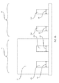
- FIG. 1 depicts a plurality of spacers 10 a , 10 b present over a semiconductor structure, e.g., semiconductor substrate 5 , formed using spacer image transfer (SIT).
- a hardmask layer 6 may be present between the semiconductor substrate 5 and the plurality of spacers 10 a , 10 b .
- a first plurality of spacers 10 a is present in a first region 15 of the semiconductor substrate 5 that is later processed to provide low voltage (SD) semiconductor devices; and a second plurality of spacers 10 b is present in a second region 20 of the semiconductor substrate 5 that is later processed to provide high voltage (EG) semiconductor devices.
- SD low voltage
- EG high voltage
- the semiconductor substrate 5 may be a bulk semiconductor substrate.
- the semiconductor substrate 5 may be composed of a type IV semiconductor material or a compound semiconductor material.
- type IV semiconductor it is meant that the semiconductor material includes at least one element from Group IVA (i.e., Group 14) of the Periodic Table of Elements.
- type IV semiconductor materials that are suitable for the fin structure include silicon (Si), germanium (Ge), silicon germanium (SiGe), silicon doped with carbon (Si:C), silicon germanium doped with carbon (SiGe:C) and a combination thereof.
- the semiconductor substrate 5 is composed of silicon (Si), e.g., single crystal silicon.
- a compound semiconductor material suitable for the semiconductor substrate is a III-V semiconductor material.
- III-V compound semiconductor denotes a semiconductor material that includes at least one element from Group III of the Periodic Table of Elements and at least one element from Group V of the Periodic Table of Elements.
- the III-V compound semiconductors are binary, ternary or quaternary alloys including III/V elements.
- III-V compound semiconductors that can be used in the present invention include, but are not limited to alloys of gallium arsenic (GaAs), aluminum arsenic (AlAs), indium gallium arsenic (InGaAs), indium aluminum arsenic (InAlAs), indium aluminum arsenic antimony (InAlAsSb), indium aluminum arsenic phosphorus (InAlAsP), indium gallium arsenic phosphorus (InGaAsP) and combinations thereof.
- GaAs gallium arsenic
- AlAs aluminum arsenic
- InGaAs indium gallium arsenic
- InAlAs indium aluminum arsenic
- InAlAsSb indium aluminum arsenic antimony
- InAlAsP indium aluminum arsenic phosphorus
- InGaAsP indium gallium arsenic phosphorus
- the semiconductor substrate may be a bulk substrate, as depicted in FIG. 1 , or the semiconductor substrate may be a semiconductor on insulator (SOI) substrate.
- SOI semiconductor on insulator
- a semiconductor on insulator (SOI) layer such as a silicon layer
- SOI semiconductor on insulator
- buried dielectric layer such as a silicon oxide layer
- the buried dielectric layer is present atop a base semiconductor layer.
- Any of the aforementioned semiconductor materials used for the semiconductor substrate may provide the composition of the SOI layer or the base semiconductor layer.
- the hardmask dielectric layer 6 may be composed of any dielectric material, such as an oxide, nitride or oxynitride material.
- the hardmask dielectric layer 6 when the hardmask dielectric layer 6 is an oxide, the hardmask dielectric layer 6 may be silicon oxide. In another example, when the hardmask dielectric layer 6 is a nitride, the hardmask dielectric layer 6 may be composed of silicon nitride. It is noted that the above compositions for the hard mask dielectric layer are provided for illustrative purposes only, as other dielectric materials typically used in semiconductor devices are equally applicable, such as aluminum oxide, silicon carbon boron nitride (SiCBN), hafnium oxide, etc.
- the hardmask dielectric layer 6 may have a thickness of 1 nm to 10 nm, and may be deposited using a chemical vapor deposition (CVD) process, such as plasma enhanced chemical vapor deposition (PECVD) or metal organic chemical vapor deposition (MOCVD). In some embodiments, the hardmask dielectric layer 6 may be omitted.
- CVD chemical vapor deposition
- PECVD plasma enhanced chemical vapor deposition
- MOCVD metal organic chemical vapor deposition
- the spacers 10 a , 10 b may be formed atop the substrate 10 using a spacer image transfer process.
- the SIT process can include forming a mandrel material layer (not shown) on the material layer that provides the fin structures, such as the SOI layer of an SOI substrate, or the bulk semiconductor substrate 5 upper surface.
- the mandrel material layer can include any material (semiconductor, dielectric or conductive) that can be selectively removed from the structure during a subsequently performed etching process.
- the mandrel material layer may be composed of amorphous silicon or polysilicon.
- the mandrel material layer may be composed of a metal, such as, e.g., aluminum (Al), tungsten (W), or copper (Cu).
- the mandrel material layer can be formed by a deposition method, such as chemical vapor deposition or plasma enhanced chemical vapor deposition.
- the thickness of the mandrel material layer can be from 50 nm to 300 nm.
- the mandrel material layer can be patterned by lithography and etching to form a plurality of mandrel structures over the topmost surface of the semiconductor containing material, e.g., overlying the semiconductor substrate 1 , that provides the fin structures.
- the SIT process may continue by forming a dielectric spacer 10 a , 10 b on each sidewall of each mandrel structure.
- the dielectric spacer 10 a , 10 b can be formed by deposition of a dielectric spacer material, and then etching the deposited dielectric spacer material.
- the dielectric spacer material may comprise any dielectric spacer material such as, for example, silicon dioxide, silicon nitride or a dielectric metal oxide. Examples of deposition processes that can be used in providing the dielectric spacer material include, but are not limited to, chemical vapor deposition (CVD), plasma enhanced chemical vapor deposition (PECVD), or atomic layer deposition (ALD).
- CVD chemical vapor deposition
- PECVD plasma enhanced chemical vapor deposition
- ALD atomic layer deposition
- etching examples include any etching process, such as, e.g., reactive ion etching (RIE). Since the dielectric spacers 10 a , 10 b are used in the SIT process as an etch mask, the width of the each dielectric spacer 10 a , 10 b determines the width of each fin structure.
- RIE reactive ion etching
- the dielectric spacers 10 a , 10 b at this stage of the process flow have a width D 1 of less than 20 nm, as measured at the base of the dielectric spacers 10 a , 10 b .
- the dielectric spacers 10 a , 10 b have a width D 1 ranging from 5 nm to 20 nm.
- each mandrel structure can be removed by an etching process that is selective for removing the mandrel material as compared to silicon.
- adjacent dielectric spacers 10 a , 10 b may be separated by a pitch P 1 , P 2 , ranging from 10 nm to 500 nm.
- the pitch P 1 , P 2 separating adjacent dielectric spacers 10 a , 10 b may range from 20 nm to 50 nm.
- the pitch P 1 of the adjacent dielectric spacers 10 a in the first region 15 of the semiconductor substrate 5 is substantially the same as the pitch P 2 of the adjacent dielectric spacers 10 b in the second region 20 of the semiconductor substrate 5 .
- FIG. 2 depicts forming a block mask 25 over a first grouping of dielectric spacers 10 a in a first region 15 of the semiconductor containing substrate 5 .
- the block mask 25 does not cover the second grouping of dielectric spacers 10 b in the second region 20 of the semiconductor containing substrate 5 leaving them exposed.
- the block mask 25 may comprise soft and/or hardmask materials and can be formed using deposition, photolithography and etching.
- the block mask 25 comprises a photoresist.
- a photoresist block mask can be produced by applying a photoresist layer, exposing the photoresist layer to a pattern of radiation, and then developing the pattern into the photoresist layer utilizing conventional resist developer.
- the block masks have a thickness ranging from 100 nm to 300 nm.
- FIG. 3 depicts one embodiment of an isotropic etch applied to the second grouping of spacers 10 b not covered by the block mask 25 , wherein the isotropic etch reduces a width of at least one spacer 10 b in the second group of spacers to a second width D 2 that is less than the first width D 1 .
- the isotropic etch reduces a width of at least one spacer 10 b in the second group of spacers to a second width D 2 that is less than the first width D 1 .
- anisotropic etching in which the etch rate in one direction exceeds the remaining directions
- isotropic etching the etch rate in substantially all directions is substantially the same.
- One example of isotropic etching processes suitable for etching the second group of spacers to the second width D 2 may be plasma etching.
- the isotropic etching of the second group of spacers 10 b may laterally remove 1 nm to 4 nm from each sidewall of each spacer, which reduces the overall width of each of the spacers in the second group of spacers 10 b by 2 nm to 8 nm. In another embodiment, the isotropic etching of the second group of spacers 10 b may laterally remove 2 nm to 3 nm from each sidewall of each spacer, which reduces the overall width of each of the spacers in the second group of spacers 10 b by 4 nm to 6 nm.
- the second width D 2 for each of the dielectric spacers 10 b at this stage of the present disclosure may be less than 15 nm, as measured at the base of the dielectric spacers 10 b .
- the dielectric spacers 10 b have a width D 2 that is 2 nm to 5 nm less than the first width D 1 .
- the block mask 25 may be removed by selective etching, chemical stripping or oxygen ashing, as depicted in FIG. 4 .
- FIG. 4 depicts one embodiment of etching a plurality of fin structures 30 a , 30 b from the semiconductor containing substrate 5 using the first grouping of spacers 10 a having the first width D 1 and the second grouping of spacers 10 b having the second width D 2 as an etch mask.
- the etch process for etching the semiconductor containing substrate 5 to form the first and second group of fin structures 30 a , 30 b may be an anisotropic etch.
- an “anisotropic etch process” denotes a material removal process in which the etch rate in the direction normal to the surface to be etched is greater than in the direction parallel to the surface to be etched.
- the anisotropic etch may include reactive-ion etching (RIE).
- Reactive Ion Etching is a form of plasma etching in which during etching the surface to be etched is placed on the RF powered electrode. Moreover, during RIE the surface to be etched takes on a potential that accelerates the etching species extracted from plasma toward the surface, in which the chemical etching reaction is taking place in the direction normal to the surface.
- anisotropic etching that can be used at this point of the present disclosure include ion beam etching, plasma etching or laser ablation.
- the etch process may also be timed and/or employ end point detection methods to determine when the etch process has recessed the exposed surfaces of the semiconductor containing substrate 5 sufficiently to provide the desired height of the fin structures 30 a , 30 b .
- the etch process is typically a selective etch.
- selective as used to describe a material removal process denotes that the rate of material removal for a first material is greater than the rate of removal for at least another material of the structure to which the material removal process is being applied.
- a selective etch may include an etch chemistry that removes a first material selectively to a second material by a ratio of 100:1 or greater.
- the etch process removes the material of the semiconductor containing substrate 5 , and the hard mask dielectric 6 , selectively to the dielectric spacers 10 a , 10 b.
- the fin structures 30 a , 30 b may have a height H 1 ranging from 5 nm to 200 nm. In another embodiment, the fin structures 30 a , 30 b may have a height H 1 ranging from 10 nm to 100 nm.
- the fin structures 30 a , 30 b have a width D 3 , D 4 that is dictated by the width D 1 , D 2 of the first and second plurality of spacers 10 a , 10 b .
- the first width D 1 of the first plurality of spacers 10 a dictates the width D 3 of the first plurality of fin structures 30 a
- the second width D 2 of the second plurality of spacer 10 b dictates the width D 4 of the second plurality of fin structures 30 b
- the pitch separating adjacent fin structures 30 a , 30 b is also set by the pitch P 1 , P 2 separating the adjacent dielectric spacers 10 a , 10 b.
- the fin structures 30 a , 30 b may be composed of a silicon including material that provides the semiconductor substrate 1 , which may include, but is not limited to silicon, single crystal silicon, multicrystalline silicon, polycrystalline silicon, amorphous silicon, strained silicon, silicon doped with carbon (Si:C), silicon alloys or any combination thereof.
- the fin structures 30 a , 30 b may also be composed of germanium including semiconductor materials, such as silicon germanium (SiGe) or germanium (Ge).
- the fin structures 30 a , 30 b may also be composed of a type III-V semiconductor material, such as gallium arsenide (GaAs).
- the space between the adjacent fin structures 30 a , 30 b is filled with a dielectric material (not shown), which may be referred to as dielectric regions or isolation regions).
- the dielectric regions may be composed of a nitride, oxide, oxynitride material, and/or any other suitable dielectric layer.
- the dielectric regions when the dielectric regions are composed of an oxide, the dielectric regions can be silicon oxide (SiO 2 ).
- the dielectric regions can be silicon nitride.
- the dielectric regions can be formed by a deposition process, such as CVD.
- CVD processes include, but not limited to, Atmospheric Pressure CVD (APCVD), Low Pressure CVD (LPCVD) and PECVD, Metal-Organic CVD (MOCVD) and combinations thereof.
- APCVD Atmospheric Pressure CVD
- LPCVD Low Pressure CVD
- PECVD PECVD
- MOCVD Metal-Organic CVD
- the dielectric regions 6 may be formed using a growth process, such as thermal oxidation or thermal nitridation.
- the dielectric regions may be recessed using a selective etch process to provide an exposed portion of the upper portion of the fins structures 30 a , 30 b .
- the dielectric regions are removed by an etch that is selective to the fin structures 5 .
- the etch process for removing the dielectric regions may be an anisotropic etch or an isotropic etch.
- the etch process may be a wet chemical etch, reactive ion etch (RIE), plasma etch, laser etch and combinations thereof.
- a gate structure may be formed on the channel region of the fin structures.
- the gate structure may be at least a partial replacement gate structure including at least one sacrificial element.
- the term “sacrificial” as used to describe the replacement gate conductor and replacement gate dielectric denotes that the structure is present during the process sequence, but is not present in the final device structure, in which the replacement structure provides an opening that dictates the size and geometry of a later formed functional gate conductor and functional gate dielectric.
- an oxide layer 35 is deposited on the first grouping of fin structures and the second grouping of fin structures. It is noted that the composition of the oxide layer and its thickness is selected for high voltage applications. Therefore, it is not entirely necessary that the oxide layer 35 be an oxide, and is hereafter referred to as high voltage dielectric layer 35 .
- the high voltage dielectric layer 35 that is present on the first group of fin structures 30 a is later removed to provide a gate structure suitable for low voltage semiconductor devices. Therefore, the high voltage dielectric layer 35 that is present on the first group of fin structures 30 a is part of the replacement gate structure in the first region 15 of the substrate.
- the high voltage dielectric layer 35 that is present on the second group of fin structures 30 b remains in the final gate structure that is present in the second region 20 of the semiconductor substrate 5 , which is suitable for high voltage semiconductor devices. Therefore, the high voltage dielectric layer 35 that is present on the second group of fin structures 30 b is part of a functional gate structure in the second region 25 of the substrate.
- the “functional gate structure” operates to switch the semiconductor device from an “on” to “off” state, and vice versa.
- the functional gate structure typically includes at least on gate dielectric and at least one gate conductor.
- the high voltage dielectric layer 35 may be composed of any dielectric material.
- the high voltage dielectric layer 35 may be composed of an oxide, such as silicon oxide.
- Silicon oxide is only one example of a dielectric composition that is suitable for the high voltage dielectric layer 35 .
- the dielectric composition of the high voltage dielectric layer may also be composed of other oxides, such as aluminum oxide and hafnium oxide; carbon doped oxide dielectrics comprised of Si, C, O, and H (SiCOH); nitrides such as silicon nitride, boron nitride, silicon carbon boron nitride (SiCBN), and oxynitrides such as silicon oxynitride, silicon carbon oxynitride, hafnium oxynitride; as well as combinations thereof.
- the high voltage dielectric layer 35 may be deposited using chemical vapor deposition. Examples of chemical vapor deposition that are suitable for forming the high voltage dielectric layer 35 include chemical vapor deposition (CVD), plasma enhanced chemical vapor deposition (PECVD), physical vapor deposition (PVD), atomic layer deposition (ALD) and other like deposition processes.
- the high voltage dielectric layer 35 may also include material layers formed using a thermal growth process, such as thermal oxidation.
- the high voltage dielectric layer 35 may have a thickness ranging from 3 nm to 10 nm. In some embodiments, the high voltage dielectric layer 35 has a thickness that ranges from 3 nm to 5 nm.
- the high voltage dielectric layer 35 may be blanket deposited on the entire substrate including the first grouping of fin structures 30 a , the second grouping of fin structures 30 b , wherein an etch process is utilized to remove the portion of the high voltage dielectric layer 35 that is present between the adjacent fin structures 30 a , 30 b.
- a sacrificial gate conductor may be formed on the high voltage dielectric layer 35 .
- the sacrificial gate conductor is a component of the replacement gate structure for each of the first and second plurality of fin structures 30 a , 30 b .
- the sacrificial material that provides the sacrificial gate structure may be composed of any material that can be etched selectively to the underlying fin structures 30 a in the first region 15 of the semiconductor substrate 1 , and the high voltage dielectric layer 35 that is present in the second region 25 of the semiconductor substrate 1 .
- the sacrificial material that provides the sacrificial gate conductor may be composed of a silicon-containing material, such as polysilicon.
- the sacrificial gate conductor is typically composed of a semiconductor material
- the sacrificial gate conductor may also be composed of a dielectric material, such as an oxide, nitride or oxynitride material, or amorphous carbon.
- the sacrificial material may be patterned and etched to provide the sacrificial gate conductor. Specifically, and in one example, a pattern is produced by applying a photoresist to the surface to be etched, exposing the photoresist to a pattern of radiation, and then developing the pattern into the photoresist utilizing a resist developer.
- the sections if the sacrificial material covered by the photoresist are protected to provide the sacrificial gate conductor, while the exposed regions are removed using a selective etching process that removes the unprotected regions.
- the photoresist may be removed.
- At least one dielectric gate spacer may then be formed on the sidewall of the sacrificial gate structures.
- the dielectric gate spacer may be formed by using a blanket layer deposition, such as CVD, and an anisotropic etchback method.
- the source and drain regions may be formed.
- the source and drain regions are formed on the source and drain region portions of the fin structures.
- the source and drain region portions of the fin structures are the portions of the fin structures that are on opposing sides of the portion of the fin structure, i.e., channel portion, that the sacrificial gate structure is present on.
- the term “drain” means a doped region in semiconductor device located at the end of the channel region, in which carriers are flowing out of the transistor through the drain.
- source is a doped region in the semiconductor device, in which majority carriers are flowing into the channel region.
- the channel region is the region between the source and drain of a semiconductor device that becomes conductive when the semiconductor device is turned on.
- the conductivity type of the source and the drain regions typically dictates the conductivity type of the semiconductor device.
- the term “conductivity type” refers to whether the device is n-type or p-type.
- the conductivity type of the source and drain regions typically dictate the conductivity type of the device. For example, if the source and drain regions are doped to an n-type conductivity, the semiconductor device may be referred to as an n-type conductivity device, such as an n-FinFET, and if the source and drain regions are doped to a p-type conductivity, the semiconductor device may be referred to as a p-type conductivity device, such as a p-FinFET.
- the source and drain regions may be formed by ion implanting n-type or p-type dopant into the source and drain region portions of the fin structures 30 a , 30 b .
- the source and drain regions may be formed by forming in-situ doped n-type or p-type conductivity epitaxial semiconductor material on the source and drain region portions of the fin structures 30 a , 30 b .
- a combination of ion implantation and in-situ doped n-type or p-type conductivity epitaxial semiconductor material may be employed to form the source and drain regions.
- Block masks may be utilized to isolate specific fin structures 30 a , 30 b for each conductivity type doping required.
- the method may continue with replacing the sacrificial gate structures with functional gate structures 50 a , 50 b .
- Substituting the sacrificial gate structure with a functional gate structure may begin with forming an interlevel dielectric layer may be formed overlying the structure, and planarizing the interlevel dielectric layer to be coplanar with an upper surface of the sacrificial gate conductor of the sacrificial gate structures.
- the sacrificial gate conductor may then be removed by an etch that is selective to the high voltage dielectric layer 35 that is present on the fins structures 35 a , 35 b .
- a first functional gate structure 50 a is formed on the first plurality of fin structures 30 a having the first width D 3
- a second functional gate structure 50 b is formed on the second plurality of fin structures 30 b having the second width D 4 .
- the first functional gate structure 50 a is formed after the high voltage dielectric layer 35 is removed from the first plurality of fin structures 30 a .
- the first functional gate structure 50 a includes a first high-k gate dielectric 51 that is in direct contact with a channel region of the first plurality of fin structures 30 a , and a first gate conductor 52 .
- the second functional gate structure 50 b that is present on the second plurality of fin structures 30 b includes the high voltage dielectric layer 35 that is in direct contact with a channel region of the second plurality of fin structures 30 b , a second high-k gate dielectric 53 and a second gate conductor 54 .
- Forming the first and second functional gate structures 50 a , 50 b may start with removing the high voltage dielectric layer 35 from the first plurality of fin structures 30 a .
- the high voltage dielectric layer 35 may be removed using an etch process that is selective to the first plurality of fin structures 30 a .
- an etch mask may be formed over the second region 25 of the substrate 1 covering the portion of the high voltage dielectric layer 35 that is present therein. The etch mask leaves the first region 15 of the substrate 1 , as well as the portion of the high voltage dielectric layer 35 exposed.
- the etch mask may be composed of a photoresist material that is patterned using photolithography.
- the etch mask is similar to the block mask 25 that is depicted in FIG. 2 . Therefore, the above description of the block mask 25 that is depicted in FIG. 2 is suitable for describing the etch mask.
- a selective etch may remove the high voltage dielectric layer from the first region 15 of the substrate 1 .
- the etch process for removing the high-voltage dielectric layer may be an anisotropic etch or an isotropic etch that is substantially selective to the first plurality of fin structures 30 a and the etch mask. Examples of etch processes that are suitable at this stage of the present process include gaseous etching, plasma etching, reactive ion etching (RIE), wet etching and combinations thereof. Removing the high voltage dielectric layer 35 from the first region 15 of the substrate exposes the channel region of the first plurality of fin structures 30 a.
- RIE reactive ion etching
- the etch process for removing the high voltage dielectric layer 35 may also remove material from the first plurality of fin structures 30 a .
- the width D 4 of each fin structure in the second plurality of fin structures 30 b is less than the width D 3 of the first plurality of fin structures 30 a .
- the etch that removes some material from the first plurality of fin structures 30 a may reduce the width W 3 of the fin structures in the first plurality of fin structures 30 a to be approximately equal to the width W 4 of the fin structures in the second plurality of fin structures 30 b .
- the width W 3 of the fin structures in the first plurality 30 a remains larger than the width W 4 of the fin structures in the second plurality of fin structures W 4 .
- the etch mask may be removed.
- the etch mask may be removed using selective etching, chemical stripping or oxygen ashing.
- a high-k gate dielectric layer 51 , 52 may be formed over the channel region of the first and second plurality of fin structures 30 a , 30 b .
- the high-k gate dielectric layer 51 that is formed on the first plurality of fin structures 30 a may be formed in direct contact with the channel region of the first plurality of fin structures 30 a .
- the high-k gate dielectric layer 52 that is formed on the second plurality of fin structures 30 b may be formed directly on the high voltage dielectric layer 35 that is in direct contact with the channel region of the second plurality of fin structures 30 b .
- the term “high-k” denotes a dielectric material having a dielectric constant greater than silicon oxide (SiO 2 ) at room temperature (20° C. to 25° C.) and atmospheric pressure (1 atm).
- a high-k dielectric material may have a dielectric constant greater than 4.0.
- the high-k gate dielectric material has a dielectric constant greater than 7.0.
- the high-k dielectric layer 51 , 52 that is formed on the first and second plurality of fin structures 30 a , 30 b is composed of a high-k oxide, such as, for example, HfO 2 , ZrO 2 , Al 2 O 3 , TiO 2 , La 2 O 3 , SrTiO 3 , LaAlO 3 , Y 2 O 3 and mixtures thereof.
- a high-k oxide such as, for example, HfO 2 , ZrO 2 , Al 2 O 3 , TiO 2 , La 2 O 3 , SrTiO 3 , LaAlO 3 , Y 2 O 3 and mixtures thereof.
- Other examples of high-k dielectric materials for the high-k dielectric layers 51 , 52 that are formed on the first and second plurality of fin structures 30 a , 30 b include hafnium silicate, hafnium silicon oxynitride or combinations thereof.
- the high-k dielectric layer 51 , 52 that are formed on the first and second plurality of fin structures 30 a , 30 b may be deposited by chemical vapor deposition (CVD).
- CVD chemical vapor deposition
- Variations of CVD processes suitable for depositing the high-k dielectric layer 51 , 52 on the first and second plurality of fin structures 30 a , 30 b include, but are not limited to, APCVD, LPCVD, PECVD, MOCVD, ALD, and combinations thereof.
- the thickness of the high-k dielectric layers 51 , 52 is greater than 0.8 nm. More typically, the high-k dielectric layers 51 , 52 have a thickness ranging from about 1.0 nm to about 60 nm.
- the method may continue with forming the functional gate structure 53 , 54 for the first and second plurality of fin structures 30 a , 30 b .
- the conductive material of the gate conductor may comprise polysilicon, SiGe, a silicide, a metal or a metal-silicon-nitride such as Ta—Si—N. Examples of metals that can be used as the gate conductor include, but are not limited to, Al, W, Cu, and Ti or other like conductive metals.
- the layer of conductive material for the gate conductor may be doped or undoped. If doped, an in-situ doping deposition process may be employed.
- a doped conductive material can be formed by deposition, ion implantation and annealing.
- the at least one gate conductor may be formed using a deposition process.
- the at least one gate conductor may be formed using may be formed using a deposition process, such as chemical vapor deposition (CVD).
- CVD chemical vapor deposition
- the at least one gate conductor is composed of a metal
- PVD physical vapor deposition
- Examples of sputtering apparatus that may be suitable for depositing the at least one gate conductor include DC diode type systems, radio frequency (RF) sputtering, magnetron sputtering, and ionized metal plasma (IMP) sputtering.
- DC diode type systems radio frequency (RF) sputtering, magnetron sputtering, and ionized metal plasma (IMP) sputtering.
- RF radio frequency
- IMP ionized metal plasma
- the functional gate structure including the high voltage dielectric layer 35 , the high-k gate dielectric layer 52 and the gate conductor 52 is resistant to pinch off effects.
- FIGS. 7-10 depict another embodiment of the present disclosure.
- the width D 5 of the fin structures 30 d for the high-voltage semiconductor devices has been reduced by isotropically etching a second plurality of fin structures 30 d , while a first plurality of fin structures 30 c being used for the low voltage semiconductor devices is being protected by a block mask 25 .
- FIG. 7 depicts forming a plurality of spacers 10 c , 10 d using spacer image transfer over a semiconductor containing substrate 1 for being patterned into fin structures.
- the plurality of spacers 10 c , 10 d , that are depicted in FIG. 7 are similar to the plurality of spacers 10 a , 10 b that are depicted in FIG. 1 . Therefore, the description of the plurality of spacers 10 a , 10 b , as well as the spacer image transfer (SIT) method for forming the plurality of spacers 10 a , 10 b that are depicted in FIG. 1 , are suitable for the description of the plurality of spacers 10 c , 10 d that are depicted in FIG.
- SIT spacer image transfer
- the width D 1 and pitch P 1 , P 2 of the spacers 10 a , 10 b depicted in FIG. 1 is suitable for the width D 1 and pitch of the spacers 10 a , 10 b that are depicted in FIG. 7 .
- the semiconductor substrate 1 that is depicted in FIG. 7 has also been described above with reference to FIG. 1 .
- FIG. 8 depicts etching a plurality of fin structures 30 c , 30 d into the semiconductor containing substrate 1 using the plurality of spacers 10 a , 10 b as an etch mask, wherein each of the fin structures 30 c , 20 d has a first width D 3 .
- the plurality of spacers 10 a , 10 b are not isotropically etched before patterning the semiconductor substrate 1 to provide the first and second plurality of fin structures 30 c , 30 d . Therefore, all of the fin structures 30 c , 30 d may have the same width D 3 at this stage of the process.
- the semiconductor substrate 1 may be etched with an anisotropic etch, such as reactive ion etch (RIE), plasma etching, laser ablation, and combinations thereof.
- the width D 3 of the fin structures 30 c , 30 d at this stage of the process flow may range from 5 nm to 20 nm.
- the height of the fin structures 30 c , 30 d at this stage of the process flow may range from 20 nm to 50 nm.
- Dielectric regions (not shown) may be formed between the adjacent fin structures providing isolation. Following fin structures 30 c , 30 d , the dielectric spacers 10 c , 10 d may be removed by selective etching, chemical stripping or oxygen ashing.
- FIG. 9 depicting forming a block mask 25 over a first grouping of fin structures 30 c in a first region 15 of the semiconductor substrate 1 , in which the second grouping of fin structures 30 d in the second region 25 of the semiconductor substrate 1 are not covered by the block mask 25 and remains exposed.
- the block mask 25 depicted in FIG. 9 is similar to the block mask 25 that is depicted in FIG. 2 . Therefore, the description of the block mask 25 that is depicted in FIG. 2 is applicable for the description of the block mask 25 depicted in FIG. 9 .
- FIG. 10 depicts one embodiment of an isotropic etch being applied to a second grouping of fin structures 30 d not covered by the block mask 25 , wherein the isotropic etch reduces a width of at least one fin structure in the second group of fin structures 30 d to a second width D 5 that is less than the first width D 3 .
- One example of isotropic etching processes suitable for etching the second group of fin structures 30 d to the second width D 5 may be plasma etching.
- the isotropic etching of the second group of fin structures 30 d may laterally remove 1 nm to 4 nm from each sidewall of each fin structure, which reduces the overall width of each of the fin structure in the second group of fin structures 30 d by 2 nm to 8 nm. In another embodiment, the isotropic etching of the second group of fin structures 30 d may laterally remove 2 nm to 3 nm from each sidewall of each fin structure, which reduces the overall width of each of the fin structures in the second group of fin structures 30 d by 4 nm to 6 nm.
- the second width D 5 for each of the fin structures 30 d at this stage of the present disclosure may be less than 15 nm, as measured at the base of the fin structure 30 d .
- the fin structures 30 d have a width D 5 that is less than the first width D 3 .
- the first plurality of fin structures 30 c may be further processed to provide low voltage semiconductor devices, and the second plurality of fin structures 30 d may be processed to provide high voltage semiconductor devices.
- a high voltage dielectric layer may be formed on each of the first and second plurality of fin structures, as described above with reference to FIG. 5 .
- Sacrificial gate structures may then be formed on each of the fin structures 30 c , 30 d , as described above. Source and drain regions may then be formed for each of the fin structures. The sacrificial gate structures may then be removed.
- the high voltage dielectric layer may be removed from the channel region of the first plurality of fin structures 30 c that provide the low voltage semiconductor device in the first region of the substrate 15 .
- Functional gate structures are then formed for each of the first and second plurality of fin structures 30 c , 30 d , as described above with reference to FIG. 6 .
- a high-k gate dielectric layer may be formed over the channel region of the first and second plurality of fin structures 30 c , 30 d .
- the high-k gate dielectric layer that is formed on the first plurality of fin structures 30 c may be formed in direct contact with the channel region of the first plurality of fin structures 30 c .
- the high-k gate dielectric layer that is formed on the second plurality of fin structures 30 d may be formed directly on the high voltage dielectric layer that is in direct contact with the channel region of the second plurality of fin structures 30 d .
- the description of the high-k dielectric layers identified by reference numbers 51 , 52 in FIG. 6 are suitable for use with the embodiments of the present disclosure using the fin structures 30 c , 30 d described with reference to FIGS.
- the method may continue with forming the conductive material of the gate conductor for the functional gate structure for each of the first and second plurality of fin structures 30 c , 30 d .
- the gate conductors identified by reference numbers 53 and 54 in FIG. 6 are suitable for use with the embodiments of the present disclosure using the fin structures 30 c , 30 d described with reference to FIGS. 7-10 .
- the process sequence for forming the finFET structure depicted in FIGS. 1-10 is formed using a gate first process sequence, which is not depicted in the supplied figures.
- the method depicted in FIGS. 1-10 is a gate last process that includes forming a replacement gate structure.
- a functional gate structure is formed instead of a replacement gate structure, and the functional gate structure remains throughout the formation of the fin structure. This is referred to as a gate first process sequence. Both gate first and gate last process sequences are applicable to the present disclosure.
- a semiconductor device includes a first plurality of fin structures 30 a , 30 c having a first width d 3 in a first region 15 of a substrate 1 , and a second plurality of fin structures 30 b , 30 d having a second width d 4 , d 5 in a second region 25 of the substrate 1 , in which second width d 4 , d 5 is less than the first width d 3 .
- the first plurality of fin structures 30 a , 30 c and the second plurality of fin structures 30 b , 30 d have substantially the same pitch P 1 , P 2 .
- a first gate structure 50 a is formed on the first plurality of fin structures 30 a , 30 c
- a second gate structure 50 b is formed on the second plurality of fin structures 30 b , 30 d .
- FIG. 6 only depicts the gate structures 50 a , 50 b being formed on the first and second plurality of fin structures 30 a , 30 b that have been formed by the process sequence depicted in FIGS. 1-6
- the gate structures 50 a , 50 b depicted in FIG. 6 may equally be present on the plurality of fin structures 30 c , 30 d formed using the method described with reference to FIGS. 1-10 .
- the first gate structure 50 a includes a first high-k gate dielectric 51 that is in direct contact with a channel region of the first plurality of fin structures 30 a , 30 c and a first gate conductor 53 .
- a second gate structure 50 b is formed on the second plurality of fin structures 30 including an oxide gate dielectric 35 , also referred to as a high voltage gate dielectric 35 , that is in direct contact with a channel region of the second plurality of fin structures 30 b , 30 d , a second high-k gate dielectric 52 and a second gate conductor 54 .
- the first gate structure 50 a may provide the gate structure for a low voltage semiconductor device, such as a low voltage FinFET.
- the low voltage Fin Field Effect Transistors that may include the first plurality of fin structures 30 a , 30 c and the first gate structure 50 a have an applied voltage of less than 1.2 V.
- the second gate structure 50 b may provide the gate structure for a high voltage semiconductor device, such as a high voltage FinFET.
- the high voltage Fin Field Effect Transistors that may include the second plurality of fin structures 30 b , 30 d and the first gate structure 50 b have an applied voltage of more than 2.0 eV.
Abstract
Description
Claims (20)
Priority Applications (2)
| Application Number | Priority Date | Filing Date | Title |
|---|---|---|---|
| US15/345,595 US9780091B2 (en) | 2015-11-23 | 2016-11-08 | Fin pitch scaling for high voltage devices and low voltage devices on the same wafer |
| US15/634,307 US10332796B2 (en) | 2015-11-23 | 2017-06-27 | Fin pitch scaling for high voltage devices and low voltage devices on the same wafer |
Applications Claiming Priority (2)
| Application Number | Priority Date | Filing Date | Title |
|---|---|---|---|
| US14/948,745 US9786563B2 (en) | 2015-11-23 | 2015-11-23 | Fin pitch scaling for high voltage devices and low voltage devices on the same wafer |
| US15/345,595 US9780091B2 (en) | 2015-11-23 | 2016-11-08 | Fin pitch scaling for high voltage devices and low voltage devices on the same wafer |
Related Parent Applications (1)
| Application Number | Title | Priority Date | Filing Date |
|---|---|---|---|
| US14/948,745 Division US9786563B2 (en) | 2015-11-23 | 2015-11-23 | Fin pitch scaling for high voltage devices and low voltage devices on the same wafer |
Related Child Applications (1)
| Application Number | Title | Priority Date | Filing Date |
|---|---|---|---|
| US15/634,307 Continuation US10332796B2 (en) | 2015-11-23 | 2017-06-27 | Fin pitch scaling for high voltage devices and low voltage devices on the same wafer |
Publications (2)
| Publication Number | Publication Date |
|---|---|
| US20170148788A1 US20170148788A1 (en) | 2017-05-25 |
| US9780091B2 true US9780091B2 (en) | 2017-10-03 |
Family
ID=58719786
Family Applications (4)
| Application Number | Title | Priority Date | Filing Date |
|---|---|---|---|
| US14/948,745 Active US9786563B2 (en) | 2015-11-23 | 2015-11-23 | Fin pitch scaling for high voltage devices and low voltage devices on the same wafer |
| US15/345,595 Active US9780091B2 (en) | 2015-11-23 | 2016-11-08 | Fin pitch scaling for high voltage devices and low voltage devices on the same wafer |
| US15/634,307 Active US10332796B2 (en) | 2015-11-23 | 2017-06-27 | Fin pitch scaling for high voltage devices and low voltage devices on the same wafer |
| US15/680,697 Active US10269644B2 (en) | 2015-11-23 | 2017-08-18 | Fin pitch scaling for high voltage devices and low voltage devices on the same wafer |
Family Applications Before (1)
| Application Number | Title | Priority Date | Filing Date |
|---|---|---|---|
| US14/948,745 Active US9786563B2 (en) | 2015-11-23 | 2015-11-23 | Fin pitch scaling for high voltage devices and low voltage devices on the same wafer |
Family Applications After (2)
| Application Number | Title | Priority Date | Filing Date |
|---|---|---|---|
| US15/634,307 Active US10332796B2 (en) | 2015-11-23 | 2017-06-27 | Fin pitch scaling for high voltage devices and low voltage devices on the same wafer |
| US15/680,697 Active US10269644B2 (en) | 2015-11-23 | 2017-08-18 | Fin pitch scaling for high voltage devices and low voltage devices on the same wafer |
Country Status (1)
| Country | Link |
|---|---|
| US (4) | US9786563B2 (en) |
Cited By (1)
| Publication number | Priority date | Publication date | Assignee | Title |
|---|---|---|---|---|
| US20170301671A1 (en) * | 2015-11-23 | 2017-10-19 | International Business Machines Corporation | Fin pitch scaling for high voltage devices and low voltage devices on the same wafer |
Families Citing this family (8)
| Publication number | Priority date | Publication date | Assignee | Title |
|---|---|---|---|---|
| US9614086B1 (en) * | 2015-12-30 | 2017-04-04 | Taiwan Semiconductor Manufacturing Company, Ltd. | Conformal source and drain contacts for multi-gate field effect transistors |
| US10032877B2 (en) * | 2016-08-02 | 2018-07-24 | Taiwan Semiconductor Manufacturing Company, Ltd. | FinFET and method of forming same |
| US10032869B2 (en) * | 2016-08-17 | 2018-07-24 | Taiwan Semiconductor Manufacturing Company, Ltd. | Fin field effect transistor (FinFET) device having position-dependent heat generation and method of making the same |
| US10692769B2 (en) | 2017-08-29 | 2020-06-23 | Taiwan Semiconductor Manufacturing Co., Ltd | Fin critical dimension loading optimization |
| DE102017126538A1 (en) * | 2017-08-29 | 2019-02-28 | Taiwan Semiconductor Manufacturing Co., Ltd. | LOAD OPTIMIZATION OF CRITICAL DIMENSIONS OF FINNEN |
| US10515954B2 (en) * | 2018-03-18 | 2019-12-24 | Taiwan Semiconductor Manufacturing Co., Ltd. | Semiconductor device having fin structures of varying dimensions |
| US10629706B2 (en) * | 2018-05-10 | 2020-04-21 | Taiwan Semiconductor Manufacturing Co., Ltd. | Fin and gate dimensions for optimizing gate formation |
| CN113327843B (en) * | 2020-02-28 | 2022-09-13 | 中芯国际集成电路制造(天津)有限公司 | Method for forming semiconductor structure |
Citations (19)
| Publication number | Priority date | Publication date | Assignee | Title |
|---|---|---|---|---|
| US6642105B2 (en) | 1999-12-24 | 2003-11-04 | Samsung Electronics Co., Ltd. | Semiconductor device having multi-gate insulating layers and methods of fabricating the same |
| US6642090B1 (en) * | 2002-06-03 | 2003-11-04 | International Business Machines Corporation | Fin FET devices from bulk semiconductor and method for forming |
| US7169670B2 (en) | 2003-08-27 | 2007-01-30 | Hynix Semiconductor Inc. | Method of forming gate oxide layer in semiconductor device |
| US7763531B2 (en) | 2004-05-25 | 2010-07-27 | International Business Machines Corporation | Method and structure to process thick and thin fins and variable fin to fin spacing |
| US7932152B2 (en) | 2008-02-05 | 2011-04-26 | Chartered Semiconductor Manufacturing, Ltd. | Method of forming a gate stack structure |
| US7994603B2 (en) | 2007-07-09 | 2011-08-09 | Sony Corporation | Semiconductor device and a method of manufacturing the same |
| US20120032732A1 (en) | 2010-01-08 | 2012-02-09 | Semiconductor Manufacturing International (Shanghai) Corporation | Hybrid integrated semiconductor tri-gate and split dual-gate finfet devices and method for manufacturing |
| US8492228B1 (en) | 2012-07-12 | 2013-07-23 | International Business Machines Corporation | Field effect transistor devices having thick gate dielectric layers and thin gate dielectric layers |
| US8722494B1 (en) | 2012-11-01 | 2014-05-13 | International Business Machines Corporation | Dual gate finFET devices |
| US20140327074A1 (en) * | 2013-05-02 | 2014-11-06 | United Microelectronics Corp. | Semiconductor integrated circuit |
| US20140353765A1 (en) | 2012-12-10 | 2014-12-04 | Globalfoundries Inc. | Double sidewall image transfer process |
| US8927432B2 (en) | 2012-06-14 | 2015-01-06 | International Business Machines Corporation | Continuously scalable width and height semiconductor fins |
| US9362179B1 (en) * | 2015-06-22 | 2016-06-07 | International Business Machines Corporation | Method to form dual channel semiconductor material fins |
| US20160351568A1 (en) * | 2015-05-29 | 2016-12-01 | Taiwan Semiconductor Manufacturing Co., Ltd. | Structure and formation method of semiconductor device structure |
| US20160379982A1 (en) * | 2015-06-23 | 2016-12-29 | Jung-Gun You | Integrated Circuit Device and Method of Manufacturing the Same |
| US20170040324A1 (en) * | 2015-08-04 | 2017-02-09 | Qualcomm Incorporated | Finfet device and method of making the same |
| US20170054027A1 (en) * | 2015-08-18 | 2017-02-23 | Broadcom Corporation | Wimpy finfet devices and methods for fabricating the same |
| US20170062561A1 (en) * | 2015-08-31 | 2017-03-02 | Taiwan Semiconductor Manufacturing Co., Ltd. | Structure and formation method of semiconductor device structure |
| US20170098581A1 (en) * | 2014-02-12 | 2017-04-06 | Taiwan Semiconductor Manufacturing Co., Ltd. | Gate structures with various widths and method for forming the same |
Family Cites Families (11)
| Publication number | Priority date | Publication date | Assignee | Title |
|---|---|---|---|---|
| US6960509B1 (en) * | 2004-06-30 | 2005-11-01 | Freescale Semiconductor, Inc. | Method of fabricating three dimensional gate structure using oxygen diffusion |
| KR101823105B1 (en) * | 2012-03-19 | 2018-01-30 | 삼성전자주식회사 | Method for fabricating field effect transistor |
| US9362404B2 (en) * | 2014-02-21 | 2016-06-07 | Taiwan Semiconductor Manufacturing Company, Ltd. | Doping for FinFET |
| US9236269B2 (en) * | 2014-04-23 | 2016-01-12 | Globalfoundries Inc. | Field effect transistor (FinFET) device with a planar block area to enable variable Fin pitch and width |
| KR102245133B1 (en) * | 2014-10-13 | 2021-04-28 | 삼성전자 주식회사 | Semiconductor device comprising finFETs(fin Field Effect Transistors) of different gate structures and method for fabricating the same |
| US9449835B2 (en) * | 2014-12-05 | 2016-09-20 | Globalfoundries Inc. | Methods of forming features having differing pitch spacing and critical dimensions |
| TW201624712A (en) * | 2014-12-26 | 2016-07-01 | 聯華電子股份有限公司 | Epitaxial structure and process thereof for forming fin-shaped field effect transistor |
| US9530646B2 (en) * | 2015-02-24 | 2016-12-27 | United Microelectronics Corp. | Method of forming a semiconductor structure |
| US9536795B2 (en) * | 2015-02-24 | 2017-01-03 | International Business Machines Corporation | Multiple threshold voltage trigate devices using 3D condensation |
| TWI664732B (en) * | 2015-06-23 | 2019-07-01 | 聯華電子股份有限公司 | Semiconductor structure and fabrication method thereof |
| US9786563B2 (en) * | 2015-11-23 | 2017-10-10 | International Business Machines Corporation | Fin pitch scaling for high voltage devices and low voltage devices on the same wafer |
-
2015
- 2015-11-23 US US14/948,745 patent/US9786563B2/en active Active
-
2016
- 2016-11-08 US US15/345,595 patent/US9780091B2/en active Active
-
2017
- 2017-06-27 US US15/634,307 patent/US10332796B2/en active Active
- 2017-08-18 US US15/680,697 patent/US10269644B2/en active Active
Patent Citations (19)
| Publication number | Priority date | Publication date | Assignee | Title |
|---|---|---|---|---|
| US6642105B2 (en) | 1999-12-24 | 2003-11-04 | Samsung Electronics Co., Ltd. | Semiconductor device having multi-gate insulating layers and methods of fabricating the same |
| US6642090B1 (en) * | 2002-06-03 | 2003-11-04 | International Business Machines Corporation | Fin FET devices from bulk semiconductor and method for forming |
| US7169670B2 (en) | 2003-08-27 | 2007-01-30 | Hynix Semiconductor Inc. | Method of forming gate oxide layer in semiconductor device |
| US7763531B2 (en) | 2004-05-25 | 2010-07-27 | International Business Machines Corporation | Method and structure to process thick and thin fins and variable fin to fin spacing |
| US7994603B2 (en) | 2007-07-09 | 2011-08-09 | Sony Corporation | Semiconductor device and a method of manufacturing the same |
| US7932152B2 (en) | 2008-02-05 | 2011-04-26 | Chartered Semiconductor Manufacturing, Ltd. | Method of forming a gate stack structure |
| US20120032732A1 (en) | 2010-01-08 | 2012-02-09 | Semiconductor Manufacturing International (Shanghai) Corporation | Hybrid integrated semiconductor tri-gate and split dual-gate finfet devices and method for manufacturing |
| US8927432B2 (en) | 2012-06-14 | 2015-01-06 | International Business Machines Corporation | Continuously scalable width and height semiconductor fins |
| US8492228B1 (en) | 2012-07-12 | 2013-07-23 | International Business Machines Corporation | Field effect transistor devices having thick gate dielectric layers and thin gate dielectric layers |
| US8722494B1 (en) | 2012-11-01 | 2014-05-13 | International Business Machines Corporation | Dual gate finFET devices |
| US20140353765A1 (en) | 2012-12-10 | 2014-12-04 | Globalfoundries Inc. | Double sidewall image transfer process |
| US20140327074A1 (en) * | 2013-05-02 | 2014-11-06 | United Microelectronics Corp. | Semiconductor integrated circuit |
| US20170098581A1 (en) * | 2014-02-12 | 2017-04-06 | Taiwan Semiconductor Manufacturing Co., Ltd. | Gate structures with various widths and method for forming the same |
| US20160351568A1 (en) * | 2015-05-29 | 2016-12-01 | Taiwan Semiconductor Manufacturing Co., Ltd. | Structure and formation method of semiconductor device structure |
| US9362179B1 (en) * | 2015-06-22 | 2016-06-07 | International Business Machines Corporation | Method to form dual channel semiconductor material fins |
| US20160379982A1 (en) * | 2015-06-23 | 2016-12-29 | Jung-Gun You | Integrated Circuit Device and Method of Manufacturing the Same |
| US20170040324A1 (en) * | 2015-08-04 | 2017-02-09 | Qualcomm Incorporated | Finfet device and method of making the same |
| US20170054027A1 (en) * | 2015-08-18 | 2017-02-23 | Broadcom Corporation | Wimpy finfet devices and methods for fabricating the same |
| US20170062561A1 (en) * | 2015-08-31 | 2017-03-02 | Taiwan Semiconductor Manufacturing Co., Ltd. | Structure and formation method of semiconductor device structure |
Non-Patent Citations (1)
| Title |
|---|
| List of IBM Patents or Patent Applications Treated as Related dated Nov. 8, 2016, 2 pages. |
Cited By (3)
| Publication number | Priority date | Publication date | Assignee | Title |
|---|---|---|---|---|
| US20170301671A1 (en) * | 2015-11-23 | 2017-10-19 | International Business Machines Corporation | Fin pitch scaling for high voltage devices and low voltage devices on the same wafer |
| US10269644B2 (en) | 2015-11-23 | 2019-04-23 | International Business Machines Corporation | Fin pitch scaling for high voltage devices and low voltage devices on the same wafer |
| US10332796B2 (en) * | 2015-11-23 | 2019-06-25 | International Business Machines Corporation | Fin pitch scaling for high voltage devices and low voltage devices on the same wafer |
Also Published As
| Publication number | Publication date |
|---|---|
| US10269644B2 (en) | 2019-04-23 |
| US20170301671A1 (en) | 2017-10-19 |
| US20170148681A1 (en) | 2017-05-25 |
| US20170148788A1 (en) | 2017-05-25 |
| US20170372968A1 (en) | 2017-12-28 |
| US9786563B2 (en) | 2017-10-10 |
| US10332796B2 (en) | 2019-06-25 |
Similar Documents
| Publication | Publication Date | Title |
|---|---|---|
| US10269644B2 (en) | Fin pitch scaling for high voltage devices and low voltage devices on the same wafer | |
| US11380590B2 (en) | Mechanisms for forming FinFET device | |
| US9929247B2 (en) | Etch stop for airgap protection | |
| US9748146B1 (en) | Single spacer for complementary metal oxide semiconductor process flow | |
| US8420464B2 (en) | Spacer as hard mask scheme for in-situ doping in CMOS finFETs | |
| US6645797B1 (en) | Method for forming fins in a FinFET device using sacrificial carbon layer | |
| US11374111B2 (en) | Forming replacement low-k spacer in tight pitch fin field effect transistors | |
| US8859355B1 (en) | Method to make dual material finFET on same substrate | |
| US9613963B2 (en) | Dual material finFET on single substrate | |
| US9899524B2 (en) | Split fin field effect transistor enabling back bias on fin type field effect transistors | |
| US9337254B1 (en) | Integrated FinFET capacitor | |
| US20110175163A1 (en) | FinFET WITH THIN GATE DIELECTRIC LAYER | |
| US9947586B2 (en) | Tunneling fin type field effect transistor with epitaxial source and drain regions | |
| US10593757B2 (en) | Integrated circuits having converted self-aligned epitaxial etch stop | |
| US11948972B2 (en) | High-voltage nano-sheet transistor | |
| US20200127097A1 (en) | Silicon germanium finfet with low gate induced drain leakage current |
Legal Events
| Date | Code | Title | Description |
|---|---|---|---|
| AS | Assignment |
Owner name: INTERNATIONAL BUSINESS MACHINES CORPORATION, NEW Y Free format text: ASSIGNMENT OF ASSIGNORS INTEREST;ASSIGNORS:BASKER, VEERARAGHAVAN S.;CHENG, KANGGUO;STANDAERT, THEODORUS E.;AND OTHERS;SIGNING DATES FROM 20151119 TO 20151120;REEL/FRAME:040247/0689 |
|
| STCF | Information on status: patent grant |
Free format text: PATENTED CASE |
|
| AS | Assignment |
Owner name: TESSERA, INC., CALIFORNIA Free format text: ASSIGNMENT OF ASSIGNORS INTEREST;ASSIGNOR:INTERNATIONAL BUSINESS MACHINES CORPORATION;REEL/FRAME:051489/0557 Effective date: 20191227 |
|
| AS | Assignment |
Owner name: BANK OF AMERICA, N.A., NORTH CAROLINA Free format text: SECURITY INTEREST;ASSIGNORS:ROVI SOLUTIONS CORPORATION;ROVI TECHNOLOGIES CORPORATION;ROVI GUIDES, INC.;AND OTHERS;REEL/FRAME:053468/0001 Effective date: 20200601 |
|
| MAFP | Maintenance fee payment |
Free format text: PAYMENT OF MAINTENANCE FEE, 4TH YEAR, LARGE ENTITY (ORIGINAL EVENT CODE: M1551); ENTITY STATUS OF PATENT OWNER: LARGE ENTITY Year of fee payment: 4 |