US9769899B2 - Illumination device and age compensation method - Google Patents
Illumination device and age compensation method Download PDFInfo
- Publication number
- US9769899B2 US9769899B2 US14/314,530 US201414314530A US9769899B2 US 9769899 B2 US9769899 B2 US 9769899B2 US 201414314530 A US201414314530 A US 201414314530A US 9769899 B2 US9769899 B2 US 9769899B2
- Authority
- US
- United States
- Prior art keywords
- led
- photocurrent
- photodetector
- values
- leds
- Prior art date
- Legal status (The legal status is an assumption and is not a legal conclusion. Google has not performed a legal analysis and makes no representation as to the accuracy of the status listed.)
- Active, expires
Links
- 238000005286 illumination Methods 0.000 title claims abstract description 301
- 238000000034 method Methods 0.000 title claims abstract description 259
- 230000004907 flux Effects 0.000 claims abstract description 136
- 230000004044 response Effects 0.000 claims abstract description 8
- 238000005259 measurement Methods 0.000 claims description 150
- 238000003860 storage Methods 0.000 claims description 11
- OAICVXFJPJFONN-UHFFFAOYSA-N Phosphorus Chemical compound [P] OAICVXFJPJFONN-UHFFFAOYSA-N 0.000 description 122
- 239000010410 layer Substances 0.000 description 56
- 239000003086 colorant Substances 0.000 description 46
- 239000000463 material Substances 0.000 description 40
- 239000000758 substrate Substances 0.000 description 33
- 230000008859 change Effects 0.000 description 28
- 230000000737 periodic effect Effects 0.000 description 24
- 238000010586 diagram Methods 0.000 description 23
- 238000001228 spectrum Methods 0.000 description 23
- 230000007423 decrease Effects 0.000 description 21
- 230000003287 optical effect Effects 0.000 description 19
- 230000001276 controlling effect Effects 0.000 description 16
- VYZAMTAEIAYCRO-UHFFFAOYSA-N Chromium Chemical compound [Cr] VYZAMTAEIAYCRO-UHFFFAOYSA-N 0.000 description 12
- 230000032683 aging Effects 0.000 description 11
- 230000008901 benefit Effects 0.000 description 11
- 230000008569 process Effects 0.000 description 11
- 239000000956 alloy Substances 0.000 description 8
- 230000003595 spectral effect Effects 0.000 description 8
- 241000023320 Luma <angiosperm> Species 0.000 description 7
- OSWPMRLSEDHDFF-UHFFFAOYSA-N methyl salicylate Chemical compound COC(=O)C1=CC=CC=C1O OSWPMRLSEDHDFF-UHFFFAOYSA-N 0.000 description 7
- RYGMFSIKBFXOCR-UHFFFAOYSA-N Copper Chemical compound [Cu] RYGMFSIKBFXOCR-UHFFFAOYSA-N 0.000 description 6
- 229910052782 aluminium Inorganic materials 0.000 description 6
- XAGFODPZIPBFFR-UHFFFAOYSA-N aluminium Chemical compound [Al] XAGFODPZIPBFFR-UHFFFAOYSA-N 0.000 description 6
- 229910052802 copper Inorganic materials 0.000 description 6
- 239000010949 copper Substances 0.000 description 6
- 230000000875 corresponding effect Effects 0.000 description 6
- 238000002955 isolation Methods 0.000 description 6
- 229910052751 metal Inorganic materials 0.000 description 6
- 239000002184 metal Substances 0.000 description 6
- 238000002156 mixing Methods 0.000 description 6
- 238000012360 testing method Methods 0.000 description 6
- 230000003679 aging effect Effects 0.000 description 5
- 238000001514 detection method Methods 0.000 description 5
- 239000002648 laminated material Substances 0.000 description 5
- 229910010293 ceramic material Inorganic materials 0.000 description 4
- 238000013461 design Methods 0.000 description 4
- 230000000694 effects Effects 0.000 description 4
- 238000012986 modification Methods 0.000 description 4
- 230000004048 modification Effects 0.000 description 4
- 239000007787 solid Substances 0.000 description 4
- 229910000838 Al alloy Inorganic materials 0.000 description 3
- 229910000881 Cu alloy Inorganic materials 0.000 description 3
- 229910045601 alloy Inorganic materials 0.000 description 3
- 239000004020 conductor Substances 0.000 description 3
- 238000007796 conventional method Methods 0.000 description 3
- PMHQVHHXPFUNSP-UHFFFAOYSA-M copper(1+);methylsulfanylmethane;bromide Chemical compound Br[Cu].CSC PMHQVHHXPFUNSP-UHFFFAOYSA-M 0.000 description 3
- 230000006870 function Effects 0.000 description 3
- 238000004519 manufacturing process Methods 0.000 description 3
- TWNQGVIAIRXVLR-UHFFFAOYSA-N oxo(oxoalumanyloxy)alumane Chemical compound O=[Al]O[Al]=O TWNQGVIAIRXVLR-UHFFFAOYSA-N 0.000 description 3
- 230000003071 parasitic effect Effects 0.000 description 3
- XUIMIQQOPSSXEZ-UHFFFAOYSA-N Silicon Chemical compound [Si] XUIMIQQOPSSXEZ-UHFFFAOYSA-N 0.000 description 2
- 230000006399 behavior Effects 0.000 description 2
- 230000009286 beneficial effect Effects 0.000 description 2
- 230000015556 catabolic process Effects 0.000 description 2
- 239000011248 coating agent Substances 0.000 description 2
- 238000000576 coating method Methods 0.000 description 2
- 230000002596 correlated effect Effects 0.000 description 2
- 230000003247 decreasing effect Effects 0.000 description 2
- 238000006731 degradation reaction Methods 0.000 description 2
- 238000000151 deposition Methods 0.000 description 2
- 239000003989 dielectric material Substances 0.000 description 2
- 238000005553 drilling Methods 0.000 description 2
- 230000004438 eyesight Effects 0.000 description 2
- 239000007769 metal material Substances 0.000 description 2
- 230000007935 neutral effect Effects 0.000 description 2
- 238000007747 plating Methods 0.000 description 2
- 229920006395 saturated elastomer Polymers 0.000 description 2
- 229910052710 silicon Inorganic materials 0.000 description 2
- 239000010703 silicon Substances 0.000 description 2
- 239000002356 single layer Substances 0.000 description 2
- 230000002277 temperature effect Effects 0.000 description 2
- 241001465805 Nymphalidae Species 0.000 description 1
- -1 YAG) Chemical compound 0.000 description 1
- PNEYBMLMFCGWSK-UHFFFAOYSA-N aluminium oxide Inorganic materials [O-2].[O-2].[O-2].[Al+3].[Al+3] PNEYBMLMFCGWSK-UHFFFAOYSA-N 0.000 description 1
- 238000013459 approach Methods 0.000 description 1
- 239000003990 capacitor Substances 0.000 description 1
- 230000004456 color vision Effects 0.000 description 1
- 238000004891 communication Methods 0.000 description 1
- 229910052593 corundum Inorganic materials 0.000 description 1
- 230000001747 exhibiting effect Effects 0.000 description 1
- 239000000383 hazardous chemical Substances 0.000 description 1
- 230000017525 heat dissipation Effects 0.000 description 1
- 230000003116 impacting effect Effects 0.000 description 1
- 239000012535 impurity Substances 0.000 description 1
- 230000002452 interceptive effect Effects 0.000 description 1
- 238000012545 processing Methods 0.000 description 1
- 238000009877 rendering Methods 0.000 description 1
- 230000002441 reversible effect Effects 0.000 description 1
- 239000004065 semiconductor Substances 0.000 description 1
- 238000000926 separation method Methods 0.000 description 1
- 230000007480 spreading Effects 0.000 description 1
- 238000003892 spreading Methods 0.000 description 1
- 230000001360 synchronised effect Effects 0.000 description 1
- 230000000007 visual effect Effects 0.000 description 1
- 229910001845 yogo sapphire Inorganic materials 0.000 description 1
Images


Classifications
-
- H—ELECTRICITY
- H05—ELECTRIC TECHNIQUES NOT OTHERWISE PROVIDED FOR
- H05B—ELECTRIC HEATING; ELECTRIC LIGHT SOURCES NOT OTHERWISE PROVIDED FOR; CIRCUIT ARRANGEMENTS FOR ELECTRIC LIGHT SOURCES, IN GENERAL
- H05B45/00—Circuit arrangements for operating light-emitting diodes [LED]
- H05B45/20—Controlling the colour of the light
-
- H05B33/0851—
-
- H05B33/0869—
-
- H05B33/0872—
-
- H—ELECTRICITY
- H05—ELECTRIC TECHNIQUES NOT OTHERWISE PROVIDED FOR
- H05B—ELECTRIC HEATING; ELECTRIC LIGHT SOURCES NOT OTHERWISE PROVIDED FOR; CIRCUIT ARRANGEMENTS FOR ELECTRIC LIGHT SOURCES, IN GENERAL
- H05B45/00—Circuit arrangements for operating light-emitting diodes [LED]
- H05B45/20—Controlling the colour of the light
- H05B45/22—Controlling the colour of the light using optical feedback
-
- G—PHYSICS
- G01—MEASURING; TESTING
- G01J—MEASUREMENT OF INTENSITY, VELOCITY, SPECTRAL CONTENT, POLARISATION, PHASE OR PULSE CHARACTERISTICS OF INFRARED, VISIBLE OR ULTRAVIOLET LIGHT; COLORIMETRY; RADIATION PYROMETRY
- G01J1/00—Photometry, e.g. photographic exposure meter
- G01J1/10—Photometry, e.g. photographic exposure meter by comparison with reference light or electric value provisionally void
- G01J1/20—Photometry, e.g. photographic exposure meter by comparison with reference light or electric value provisionally void intensity of the measured or reference value being varied to equalise their effects at the detectors, e.g. by varying incidence angle
- G01J1/28—Photometry, e.g. photographic exposure meter by comparison with reference light or electric value provisionally void intensity of the measured or reference value being varied to equalise their effects at the detectors, e.g. by varying incidence angle using variation of intensity or distance of source
- G01J1/30—Photometry, e.g. photographic exposure meter by comparison with reference light or electric value provisionally void intensity of the measured or reference value being varied to equalise their effects at the detectors, e.g. by varying incidence angle using variation of intensity or distance of source using electric radiation detectors
- G01J1/32—Photometry, e.g. photographic exposure meter by comparison with reference light or electric value provisionally void intensity of the measured or reference value being varied to equalise their effects at the detectors, e.g. by varying incidence angle using variation of intensity or distance of source using electric radiation detectors adapted for automatic variation of the measured or reference value
-
- H05B37/02—
-
- H—ELECTRICITY
- H05—ELECTRIC TECHNIQUES NOT OTHERWISE PROVIDED FOR
- H05B—ELECTRIC HEATING; ELECTRIC LIGHT SOURCES NOT OTHERWISE PROVIDED FOR; CIRCUIT ARRANGEMENTS FOR ELECTRIC LIGHT SOURCES, IN GENERAL
- H05B47/00—Circuit arrangements for operating light sources in general, i.e. where the type of light source is not relevant
- H05B47/10—Controlling the light source
-
- Y—GENERAL TAGGING OF NEW TECHNOLOGICAL DEVELOPMENTS; GENERAL TAGGING OF CROSS-SECTIONAL TECHNOLOGIES SPANNING OVER SEVERAL SECTIONS OF THE IPC; TECHNICAL SUBJECTS COVERED BY FORMER USPC CROSS-REFERENCE ART COLLECTIONS [XRACs] AND DIGESTS
- Y02—TECHNOLOGIES OR APPLICATIONS FOR MITIGATION OR ADAPTATION AGAINST CLIMATE CHANGE
- Y02B—CLIMATE CHANGE MITIGATION TECHNOLOGIES RELATED TO BUILDINGS, e.g. HOUSING, HOUSE APPLIANCES OR RELATED END-USER APPLICATIONS
- Y02B20/00—Energy efficient lighting technologies, e.g. halogen lamps or gas discharge lamps
- Y02B20/40—Control techniques providing energy savings, e.g. smart controller or presence detection
-
- Y02B20/46—
Definitions
- This invention relates to illumination devices comprising a plurality of light emitting diodes (LEDs) and, more particularly, to illumination devices and methods for controlling an illumination device, so as to obtain a desired luminous flux and a desired chromaticity of the device over time as the LEDs age.
- LEDs light emitting diodes
- LEDs light emitting diodes
- LEDs provide a number of advantages over traditional light sources, such as incandescent and fluorescent light bulbs, including low power consumption, long lifetime, no hazardous materials, and additional specific advantages for different applications.
- LEDs provide the opportunity to adjust the color (e.g., from white, to blue, to green, etc.) or the color temperature (e.g., from “warm white” to “cool white”) to produce different lighting effects.
- LEDs have many advantages over conventional light sources, one disadvantage of LEDs is that their output characteristics (e.g., luminous flux and chromaticity) vary over changes in drive current, temperature and over time as the LEDs age. These effects are particularly evident in multi-colored LED illumination devices, which combine a number of differently colored emission LEDs into a single package.
- output characteristics e.g., luminous flux and chromaticity
- An example of a multi-colored LED illumination device is one in which two or more different colors of LEDs are combined within the same package to produce white or near-white light.
- white light lamps There are many different types of white light lamps on the market, some of which combine red, green and blue (RGB) LEDs, red, green, blue and yellow (RGBY) LEDs, phosphor-converted white and red (WR) LEDs, RGBW LEDs, etc.
- these lamps may be configured to generate white or near-white light within a wide gamut of color points or correlated color temperatures (CCTs) ranging from “warm white” (e.g., roughly 2600K-3700K), to “neutral white” (e.g., 3700K-5000K) to “cool white” (e.g., 5000K-8300K).
- CCTs correlated color temperatures
- Some multi-colored LED illumination devices also enable the brightness and/or color of the illumination to be changed to a particular set point.
- These tunable illumination devices should all produce the same color and color rendering index (CRI) when set to a particular dimming level and chromaticity setting (or color set point) on a standardized chromacity diagram.
- a chromaticity diagram maps the gamut of colors the human eye can perceive in terms of chromacity coordinates and spectral wavelengths.
- the spectral wavelengths of all saturated colors are distributed around the edge of an outlined space (called the “gamut” of human vision), which encompasses all of the hues perceived by the human eye.
- the curved edge of the gamut is called the spectral locus and corresponds to monochromatic light, with each point representing a pure hue of a single wavelength.
- the straight edge on the lower part of the gamut is called the line of purples.
- colors within the gamut of human vision are mapped in terms of chromaticity coordinates (x, y).
- a red (R) LED with a peak wavelength of 625 nm may have a chromaticity coordinate of (0.69, 0.31)
- a green (G) LED with a peak wavelength of 528 nm may have a chromaticity coordinate of (0.18, 0.73)
- a blue (B) LED with a peak wavelength of 460 nm may have a chromaticity coordinate of (0.14, 0.04).
- the chromaticity coordinates i.e., color points
- Color points that lie on or near the blackbody locus provide a range of white or near-white light with color temperatures ranging between approximately 2500K and 10,000K.
- These color points are typically achieved by mixing light from two or more differently colored LEDs. For example, light emitted from the RGB LEDs shown in FIG. 1 may be mixed to produce a substantially white light with a color temperature in the range of about 2500K to about 5000K.
- an illumination device is typically configured to produce a range of white or near-white color temperatures arranged along the blackbody curve (e.g., about 2500K to 5000K)
- some illumination devices may be configured to produce any color within the color gamut 18 (triangle) formed by the individual LEDs (e.g., RGB).
- the chromaticity coordinates of the combined light e.g., (0.437, 0.404) for 3000K white light, define the target chromaticity or color set point at which the device is intended to operate.
- the target chromaticity or color set point may be changed by altering the ratio of drive currents supplied to the individual LEDs.
- the target chromaticity of the illumination device may be changed by adjusting the drive current levels (in current dimming) or duty cycle (in PWM dimming) supplied to one or more of the emission LEDs.
- an illumination device comprising RGB LEDs may be configured to produce “warmer” white light by increasing the drive current supplied to the red LEDs and decreasing the drive currents supplied to the blue and/or green LEDs. Since adjusting the drive currents also affects the lumen output and temperature of the illumination device, the target chromaticity must be carefully calibrated and controlled to ensure that the actual chromaticity equals the target value. Most prior art illumination devices fail to provide an accurate calibration and compensation method for controlling the color of the illumination device.
- Some prior art illumination devices also provide dimming capabilities, i.e., the ability to change the brightness or luminous flux output from the emission LEDs, in addition to (or instead of) color tuning.
- the dimming level is changed by adjusting the drive current levels (in current dimming) or the duty cycle of the drive currents (in PWM dimming) supplied to all emission LEDs to produce a target dimming level.
- adjusting the supplied drive currents changes the chromaticity of the illumination, and this change in chromaticity differs for different LED devices and different dimming methods.
- the chromaticity of an RGB LED illumination device may change rather significantly with changes drive current level and duty cycle, while the chromaticity of a phosphor-converted white LED illumination device is more consistent.
- a range of target chromaticity values must be carefully calibrated over a range of target dimming levels.
- the lumen output and chromaticity produced by prior art illumination devices often differs from the target dimming level and target chromaticity setting, due to changes in temperature and over time as the LEDs age.
- changes in temperature affect the lumen output and chromaticity of all phosphor converted and non-phosphor converted LEDs.
- prior art devices may perform some level of temperature compensation, they fail to provide accurate results by failing to recognize that temperature affects the lumen output and chromaticity of different colors of LEDs differently.
- these prior art devices fail to account for chromaticity shifts in the illumination produced by phosphor converted LEDs, which result from phosphor aging. As a consequence, these prior art devices cannot maintain a desired luminous flux and a desired chromaticity for an LED illumination device over operating conditions and over the lifetime of the illumination device.
- This need is particularly warranted in multi-color LED illumination devices, since different colors of LEDs are affected differently by temperature and age, and in tunable illumination devices that enable the target dimming level and/or the target chromaticity setting to be changed by adjusting the drive currents supplied to one or more of the LEDs, since changes in drive current inherently affect the lumen output, color and temperature of the illumination device.
- a method for controlling an LED illumination device, so that a desired luminous flux and a desired chromaticity of the device can be maintained over time as the LEDs age.
- the illumination device described herein may include a plurality of emission LEDs, or a plurality of chains of emission LEDs, and at least one dedicated photodetector.
- the term “LED” will be used herein to refer to a single LED or a chain of serially connected LEDs supplied with the same drive current.
- the method described herein may begin by applying drive currents to the plurality of LED chains substantially continuously to produce illumination, measuring a photocurrent induced on the photodetector in response to the illumination produced by each LED chain, one LED chain at a time, and received by the photodetector, and measuring a forward voltage developed across the photodetector by applying a non-operative drive current to the photodetector.
- the method may further include periodically turning the plurality of LED chains off for short durations of time, and measuring the photocurrents induced on the photodetector and the forward voltage developed across the photodetector, one at a time, during the short durations of time.
- the method described herein may further include determining, for each LED chain, an expected photocurrent value corresponding to the forward voltage measured across the photodetector and the drive current currently applied to the LED chain by applying one or more interpolation techniques to a table of stored calibration values correlating forward voltage and photocurrent to drive current at a plurality of different temperatures.
- the table of stored calibration values may include, for each LED chain, a first plurality of stored photocurrent values, a second plurality of stored photocurrent values and a plurality of stored forward voltage values.
- the first plurality of stored photocurrent values may be ones, which were previously obtained from the photodetector upon receiving illumination from the LED chain when the LED chain was subjected to a first temperature and a plurality of drive currents were successively applied to the LED chain.
- the second plurality of stored photocurrent values may be ones, which were previously obtained from the photodetector upon receiving illumination from the LED chain when the LED chain was subjected to a second temperature and the plurality of drive currents were successively applied to the LED chain.
- the plurality of stored forward voltage values may be ones, which were previously obtained across the photodetector after obtaining each of the first and second plurality of photocurrent values.
- the first plurality of stored photocurrent values, the second plurality of stored photocurrent values and the plurality of stored forward voltage values may comprise measured values.
- the measured values may be used to calculate calibration coefficients, which are stored within the table of stored calibration values in addition to, or in lieu of, the measured values.
- an expected photocurrent value for each LED may be determined by calculating a third plurality of photocurrent values corresponding to the measured forward voltage by interpolating between the first plurality of stored photocurrent values and the second plurality of stored photocurrent values corresponding to the LED chain, generating a relationship between the third plurality of photocurrent values, and selecting the expected photocurrent value from the generated relationship that corresponds to the drive current currently applied to the LED chain.
- the third plurality of photocurrent values may be calculated by using a non-linear interpolation technique to interpolate between the first and second plurality of stored photocurrent values corresponding to the LED chain.
- the relationship may be generated by applying a higher-order interpolation to the third plurality of photocurrent values to generate a non-linear relationship between photocurrent and drive current for the LED chain. In other cases, however, the relationship may be generated by applying a piece-wise linear interpolation to the third plurality of photocurrent values to approximate a non-linear relationship between photocurrent and drive current for the LED chain.
- the method described herein may further include adjusting, for each LED chain, the drive current currently applied to the LED chain if a difference exists between the expected photocurrent value and the measured photocurrent.
- the drive current may be adjusted by calculating a scale factor for the LED chain by dividing the expected photocurrent value by the measured photocurrent, applying the scale factor to a desired luminous flux value for the LED chain to obtain an adjusted luminous flux value, and adjusting the drive current currently applied to the LED chain to achieve the adjusted luminous flux value.
- an illumination device is provided herein with a plurality of light emitting diode (LED) chains, an LED driver and receiver circuit, a photodetector, a storage medium and a control circuit.
- the plurality of light emitting diode (LED) chains may be generally configured to produce illumination for the illumination device.
- the photodetector may be generally configured for detecting the illumination produced by the plurality of LED chains.
- the storage medium may be generally configured for storing a table of calibration values correlating forward voltages and photocurrents that were previously measured from the photodetector to drive currents that were previously applied to each of the LED chains at a plurality of different temperatures during calibration of the illumination device.
- the LED driver and receiver circuit may be generally configured for applying drive currents to the plurality of LED chains substantially continuously to produce the illumination.
- the LED driver and receiver circuit may be further configured for measuring a photocurrent induced on the photodetector in response to the illumination produced by each LED chain, one LED chain at a time, and received by the photodetector, measuring a forward voltage developed across the photodetector to provide a current measurement of temperature, and supplying the measured photocurrents and the measured forward voltage to the control circuit.
- the control circuit may be coupled to the LED driver and receiver circuit, the photodetector and the storage medium, and may be generally configured for determining an expected photocurrent value for each LED chain from the stored table of calibration values using the current measurement of temperature and the drive currents currently applied to each LED chain.
- the control circuit may be further configured for adjusting the drive current currently applied by the LED driver and receiver circuit to each LED chain to produce illumination, if the expected photocurrent value determined by the control circuit for the LED chain differs from the photocurrent measured by the LED driver and receiver circuit for the LED chain.
- control circuit may be configured for calculating a scale factor by dividing the expected photocurrent value by the photocurrent measured by the LED driver and receiver circuit, applying the scale factor to a desired luminous flux value to obtain an adjusted luminous flux value, and adjusting the drive current currently applied to the LED chain to achieve the adjusted luminous flux value.
- control circuit may be configured for determining the expected photocurrent value for each LED chain by using the forward voltage measured by the LED driver and receiver circuit, the drive current currently applied by the LED driver and receiver circuit to the LED chain to produce illumination, the table of calibration values and one or more interpolation techniques.
- the table of calibration values may include, for each LED chain, a first plurality of stored photocurrent values, a second plurality of stored photocurrent values, and a plurality of stored forward voltage values.
- the first plurality of stored photocurrent values may be ones, which were previously obtained from the photodetector upon receiving illumination from the LED chain when the LED chain was subjected to a first temperature and a plurality of drive currents were successively applied to the LED chain.
- the second plurality of stored photocurrent values may be ones, which were previously obtained from the photodetector upon receiving illumination from the LED chain when the LED chain was subjected to a second temperature and the plurality of drive currents were successively applied to the LED chain.
- the plurality of stored forward voltage values may be ones, which were previously measured across the photodetector before, during or after each of the first and second plurality of photocurrents were obtained.
- the first plurality of stored photocurrent values, the second plurality of stored photocurrent values and the plurality of stored forward voltage values may comprise measured values.
- the measured values may be used to calculate calibration coefficients, which are stored within the table of calibration values in addition to, or in lieu of, the measured values.
- control circuit may be configured for determining the expected photocurrent value for each LED chain by calculating a third plurality of photocurrent values corresponding to the forward voltage measured by the LED driver and receiver circuit by interpolating between the first plurality of stored photocurrent values and the second plurality of stored photocurrent values corresponding to the LED chain, generating a relationship between the third plurality of photocurrent values, and selecting the expected photocurrent value from the generated relationship that corresponds to the drive current currently applied by the LED driver and receiver circuit to the LED chain.
- control circuit may be configured to calculate the third plurality of photocurrent values by using a non-linear interpolation technique to interpolate between the first and second plurality of stored photocurrent values.
- control circuit may be configured to generate the relationship by applying a higher-order interpolation to the third plurality of photocurrent values to generate a non-linear relationship between photocurrent and drive current for the LED chain. In other cases, the control circuit may be configured to generate the relationship by applying a piece-wise linear interpolation to the third plurality of photocurrent values to approximate a non-linear relationship between photocurrent and drive current for the LED chain.
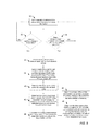
- FIG. 1 is a graph of the 1931 CIE chromaticity diagram illustrating the gamut of human color perception and the gamut achievable by an illumination device comprising a plurality of multiple color LEDs (e.g., red, green and blue);
- a plurality of multiple color LEDs e.g., red, green and blue
- FIG. 2 is a graph illustrating the non-linear relationship between relative luminous flux and junction temperature for white, blue and green LEDs
- FIG. 3 is a graph illustrating the substantially more non-linear relationship between relative luminous flux and junction temperature for red, red-orange and yellow (amber) LEDs;
- FIG. 4 is a graph illustrating the non-linear relationship between relative luminous flux and drive current for red and red-orange LEDs
- FIG. 5 is a graph illustrating the substantially more non-linear relationship between relative luminous flux and drive current for white, blue and green LEDs
- FIG. 6 is a flow chart diagram of an improved method for calibrating an illumination device comprising a plurality of LEDs and one or more photodetectors, in accordance with one embodiment of the invention
- FIG. 7 is a chart illustrating an exemplary table of calibration values that may be obtained in accordance with the calibration method of FIG. 6 and stored within the illumination device;
- FIG. 8 is a flowchart diagram of an improved compensation method, in accordance with one embodiment of the invention.
- FIG. 9 is an exemplary timing diagram for an illumination device comprising four emission LEDs, illustrating the periodic intervals during which measurements (e.g., emitter forward voltage) are obtained from each emission LED, one LED at a time;
- measurements e.g., emitter forward voltage
- FIG. 10 is a graphical representation depicting how one or more interpolation technique(s) may be used in the compensation method of FIG. 8 to determine the drive current needed to produce a desired luminous flux for a given LED using the calibration values obtained during the calibration method of FIG. 6 and stored within the illumination device;
- FIG. 11 is a graphical representation depicting how one or more interpolation technique(s) may be used in the compensation method of FIG. 8 to determine the expected x chromaticity value for a given LED using the present forward voltage, the present drive current and the calibration values obtained during the calibration method of FIG. 6 and stored within the illumination device;
- FIG. 12 is a graphical representation depicting how one or more interpolation technique(s) may be used in the compensation method of FIG. 8 to determine the expected y chromaticity value for a given LED using the present forward voltage, the present drive current and the calibration values obtained during the calibration method of FIG. 6 and stored within the illumination device;
- FIG. 13 is a flowchart diagram of an improved compensation method, in accordance with another embodiment of the invention.
- FIG. 14 is an exemplary timing diagram for an illumination device comprising four emission LEDs, illustrating the periodic intervals during which measurements are obtained from the one or more photodetectors (e.g., induced photocurrent and detector forward voltage) and from each emission LED, one LED at a time (e.g., emitter forward voltage);
- the one or more photodetectors e.g., induced photocurrent and detector forward voltage
- FIG. 15 is a graphical representation depicting how one or more interpolation technique(s) may be used in the compensation method of FIG. 13 to determine the expected photocurrent value for a given LED using the present forward voltage, the present drive current and the calibration values obtained during the calibration method of FIG. 6 and stored within the illumination device;
- FIG. 16A is a photograph of an exemplary illumination device
- FIG. 16B is a computer generated image showing a top view of an exemplary emitter module that may be included within the exemplary illumination device of FIG. 16A ;
- FIG. 17A is a photograph of another exemplary illumination device
- FIG. 17B is a computer generated image showing a top view of an exemplary emitter module that may be included within the exemplary illumination device of FIG. 17A ;
- FIG. 18A is a side view of an improved emitter module, according to one embodiment of the invention.
- FIG. 18B is a side view of an improved emitter module, according to another embodiment of the invention.
- FIG. 19 is an exemplary block diagram of circuit components that may be included within an illumination device, according to one embodiment of the invention.
- FIG. 20 is an exemplary block diagram of an LED driver and receiver circuit that may be included within the illumination device of FIG. 19 , according to one embodiment of the invention.
- FIG. 21 is an exemplary graph depicting how the spectrum of a phosphor converted LED may be divided into two portions, and showing how the phosphor efficiency decreases as the phosphor ages.
- An LED generally comprises a chip of semiconducting material doped with impurities to create a p-n junction.
- current flows easily from the p-side, or anode, to the n-side, or cathode, but not in the reverse direction.
- Charge-carriers electrons and holes—flow into the junction from electrodes with different voltages.
- the wavelength of the light emitted by the LED depends on the band gap energy of the materials forming the p-n junction of the LED.
- Red and yellow LEDs are commonly composed of materials (e.g., AlInGaP) having a relatively low band gap energy, and thus produce longer wavelengths of light. For example, most red and yellow LEDs have a peak wavelength in the range of approximately 610-650 nm and approximately 580-600 nm, respectively.
- green and blue LEDs are commonly composed of materials (e.g., GaN or InGaN) having a larger band gap energy, and thus, produce shorter wavelengths of light. For example, most green and blue LEDs have a peak wavelength in the range of approximately 515-550 nm and approximately 450-490 nm, respectively.
- a “white” LED may be formed by covering or coating, e.g., a blue LED having a peak emission wavelength of about 450-490 nm with a phosphor (e.g., YAG), which down-converts the photons emitted by the blue LED to a lower energy level, or a longer peak emission wavelength, such as about 525 nm to about 600 nm.
- a phosphor e.g., YAG
- YAG a phosphor
- such an LED may be configured to produce substantially white light having a correlated color temperature (CCT) of about 3000K.
- CCT correlated color temperature
- differently colored LEDs may be combined to produce white or near-white light within a wide gamut of color points or CCTs ranging from “warm white” (e.g., roughly 2600K-3000K), to “neutral white” (e.g., 3000K-4000K) to “cool white” (e.g., 4000K-8300K).
- white light illumination devices include, but are not limited to, those that combine red, green and blue (RGB) LEDs, red, green, blue and yellow (RGBY) LEDs, white and red (WR) LEDs, and RGBW LEDs.
- the present invention is generally directed to illumination devices having a plurality of light emitting diodes (LEDs) and one or more photodetectors.
- LED light emitting diodes
- the term “LED” will be used throughout this disclosure to refer to a single LED, or a chain of serially connected LEDs supplied with the same drive current.
- the present invention provides improved methods for calibrating and compensating individual LEDs within an LED illumination device, so as to accurately maintain a desired luminous flux and a desired chromaticity for the illumination device over changes in drive current, temperature and/or time.
- the present invention is particularly well suited to illumination devices (i.e., multi-colored illumination devices) in which two or more different colors of LEDs are combined to produce blended white or near-white light, since the output characteristics of differently colored LEDs vary differently over drive current, temperature and time.
- illumination devices i.e., tunable illumination devices
- the target dimming level and/or the target chromaticity setting to be changed by adjusting the drive currents supplied to one or more of the LEDs, since changes in drive current inherently affect the lumen output, color and temperature of the illumination device.
- FIGS. 2-3 illustrate how the relative luminous flux of an individual LED changes over junction temperature for different colors of LEDs.
- the luminous flux output from all LEDs generally decreases with increasing temperature.
- the relationship between luminous flux and junction temperature is relatively linear (see FIG. 2 ), while for other colors (e.g., red, orange and especially yellow) the relationship is significantly non-linear (see, FIG. 3 ).
- the chromaticity of an LED also changes with temperature, due to shifts in the dominant wavelength (for both phosphor converted and non-phosphor converted LEDs) and changes in the phosphor efficiency (for phosphor converted LEDs).
- the peak emission wavelength of green LEDs tends to decrease with increasing temperature, while the peak emission wavelength of red and blue LEDs tends to increase with increasing temperature. While the change in chromacity is relatively linear with temperature for most colors, red and yellow LEDs tend to exhibit a more significant non-linear change.
- the luminous flux output from both phosphor converted and non-phosphor converted LEDs, and the chromaticity of phosphor converted LEDs also changes over time.
- the luminous flux can either increase (get brighter) or decrease (get dimmer), while late in life, the luminous flux generally decreases.
- the lumen output decreases faster over time when the LEDs are subjected to higher drive currents and higher temperatures.
- the phosphor converted LED ages, the phosphor becomes less efficient and the amount of blue light that passes through the phosphor increases. This decrease in phosphor efficiency causes the overall color produced by the phosphor converted LED to appear “cooler” over time.
- the dominant wavelength and chromaticity of a non-phosphor converted LED does not change over time, the luminous flux decreases as the LED ages, which in effect causes the chromaticity of a multi-colored LED illumination device to change over time.
- the color point of the resulting device often changes significantly with variations in temperature and over time. For example, when red, green and blue LEDs are combined within a white light illumination device, the color point of the device may appear increasingly “cooler” as the temperature rises. This is because the luminous flux produced by the red LEDs decreases significantly as temperatures increase, while the luminous flux produced by the green and blue LEDs remains relatively stable (see, FIGS. 2-3 ).
- some prior art illumination devices attempt to maintain a consistent lumen output and/or a consistent chromaticity over temperature and time by measuring characteristics of the emission LEDs and increasing the drive current supplied to one or more of the emission LEDs. For example, some prior art illumination devices measure the temperature of the illumination device (either directly through an ambient temperature sensor or heat sink measurement, or indirectly through a forward voltage measurement), and adjust the drive currents supplied to one or more of the emission LEDs to account for temperature related changes in lumen output. Other prior art illumination devices measure the lumen output from individual emission LEDs, and if the measured value differs from a target value, the drive currents supplied to the emission LED are increased to account for changes in luminous flux that occur over time.
- FIGS. 4 and 5 illustrate the relationship between luminous flux and drive current for different colors of LEDs (e.g., red, red-orange, white, blue and green LEDs).
- the luminous flux increases with larger drive currents, and decreases with smaller drive currents.
- the change in luminous flux with drive current is non-linear for all colors of LEDs, and this non-linear relationship is substantially more pronounced for certain colors of LEDs (e.g., blue and green LEDs) than others.
- the chromaticity of the illumination also changes when drive currents are increased to combat temperature and/or aging effects, since larger drive currents inherently result in higher LED junction temperatures (see, FIGS. 2-3 ). While the change in chromaticity with drive current/temperature is relatively linear for all colors of LEDs, the rate of change is different for different LED colors and even from part to part.
- prior art illumination devices may adjust the drive currents supplied to the emission LEDs, these devices fail to provide accurate temperature and age compensation by failing to account for the non-linear relationship that exists between luminous flux and junction temperature for certain colors of LEDs ( FIGS. 2-3 ), the non-linear relationship that exists between luminous flux and drive current for all colors of LEDs ( FIGS. 4-5 ), and the fact that these relationships differ for different colors of LEDs. These devices also fail to account for the fact that the rate of change in chromaticity with drive current/temperature is different for different colors of LEDs. Without accounting for these behaviors, prior art illumination devices cannot provide accurate temperature and age compensation for all LEDs included within a multi-colored LED illumination device.
- This need is particularly relevant to multi-colored LED illumination devices, since different LED colors respond differently over temperature and time, and to illumination devices that provide dimming and/or color tuning capabilities, since changes in drive current inherently affect the lumen output, color and temperature of the illumination device.
- improved illumination devices and methods are provided herein to individually calibrate and compensate each LED used in the LED illumination device.
- the improved calibration and compensation methods described herein overcome the disadvantages of conventional methods, which fail to provide accurate temperature and age compensation for all LEDs included within an LED illumination device.
- FIG. 6 illustrates one embodiment of an improved method for calibrating an illumination device comprising a plurality of LEDs and at least one dedicated photodetector.
- the calibration method shown in FIG. 6 may be used to calibrate an illumination device having LEDs all of the same color.
- the calibration method described herein is particularly well-suited for calibrating an illumination device comprising two or more differently colored LEDs (i.e., a multi-colored LED illumination device), since output characteristics of differently colored LEDs vary differently over drive current, temperature and time.
- the calibration method described herein is also particularly well-suited for calibrating an illumination device that provides dimming and/or color tuning capabilities (i.e., a tunable LED illumination device), since changes in drive current inherently affect the lumen output, color and temperature of the illumination device.
- a tunable LED illumination device i.e., a tunable LED illumination device
- each emitter module may generally include a plurality of emission LEDs arranged in an array, and at least one dedicated photodetector spaced about a periphery of the array.
- the array of emission LEDs may include red, green, blue and white (or yellow) LEDs
- the at least one dedicated photodetector may include one or more red, orange, yellow and/or green LEDs.
- the present invention is not limited to any particular color, number, combination or arrangement of emission LEDs or photodetectors. A skilled artisan would understand how the method steps described herein may be applied to other LED illumination devices having substantially different emitter modules.
- the improved calibration method may generally begin by subjecting the illumination device to a first ambient temperature (in step 10 ). Once subjected to this temperature, a plurality of different drive current levels may be applied to the emission LEDs (in step 12 ) and a plurality of measurements may be obtained from both the emission LEDs and the dedicated photodetector LED(s) at each of the different drive current levels (in steps 14 and 16 ). Specifically, two or more different drive current levels may be successively applied to each emission LED, one LED at a time, for the purpose of obtaining measurements from the illumination device. These measurements may generally include optical measurements and electrical measurements.
- a plurality of optical measurements may be obtained from the illumination produced by each emission LED at each of the different drive current levels (in step 14 ).
- the optical measurements may include a plurality of luminous flux, x chromaticity and y chromaticity measurements, which are obtained for each emission LED at two or more different drive current levels.
- the optical measurements described herein are not limited to luminous flux, x chromaticity and y chromaticity, and may include additional or alternative optical measurements in other embodiments of the invention.
- the chromaticity calibration values described herein may correspond to the CIE 1931 XYZ color space, the CIE 1931 RGB color space, the CIE 1976 LUV color space, and various other RGB color spaces (e.g., sRGB, Adobe RGB, etc.).
- RGB color spaces e.g., sRGB, Adobe RGB, etc.
- the calibration and compensation methods described herein acquire and utilize only x and y chromaticity calibration values, one skilled in the art would understand how chromaticity values from other color spaces could be alternatively acquired and used in the methods described herein.
- the calibration and compensation methods described herein and recited in the claims are considered to encompass chromaticity calibration values from any color space that can be used to describe the gamut of an LED illumination device comprising substantially any combination of emission LEDs as described herein.
- three luminous flux (Luma) measurements, three x chromaticity (x chrom) measurements, and three y chromaticity (y chrom) measurements are measured from each emission LED at roughly a maximum drive current level (typically about 500 mA, depending on LED part number and manufacturer), roughly 30% of the maximum drive current, and roughly 10% of the maximum drive current, as shown in FIG. 7 and discussed below.
- the luminous flux and x, y chromaticity measurements may be obtained from the emission LEDs using an external calibration tool, such as a spectrophotometer.
- the measurement values obtained from the external calibration tool may be transmitted wirelessly to the illumination device, as described in more detail below with respect to FIG. 19 .
- a plurality of electrical measurements may be obtained from each of the emission LEDs and each of the dedicated photodetector(s) at each of the different drive current levels (in step 16 ).
- These electrical measurements may include, but are not limited to, photocurrents induced on the dedicated photodetector(s) and forward voltages measured across the dedicated photodetector(s) and/or the emission LEDs.
- the electrical measurements may be obtained from the dedicated photodetector(s) and the emission LEDs using the LED driver and receiver circuit included within the illumination device. An exemplary embodiment of such a circuit is shown in FIGS. 19-20 and described in more detail below.
- the LED driver and receiver circuit measures the photocurrents that are induced on the dedicated photodetector by the illumination individually produced by each emission LED.
- three photocurrent (Iph_d 1 ) measurements may be obtained from the dedicated photodetector for each emission LED when the emission LEDs are successively driven to produce illumination at three different drive current levels (e.g., 100%, 30% and 10% of a max drive level).
- the LED driver and receiver circuit may obtain the photocurrent (Iph_d 1 ) measurements at substantially the same time the external calibration tool is measuring the luminous flux and x and y chromaticity of the illumination produced by the emission LEDs at each of the different drive current levels.
- the drive currents applied to the emission LEDs to measure luminous flux, chromaticity and induced photocurrent may be operative drive current levels (e.g., about 20 mA to about 500 mA). In some cases, increasingly greater drive current levels may be successively applied to each of the emission LEDs to obtain the measurements described herein. In other cases, the measurements may be obtained upon successively applying decreasing levels of drive current to the emission LEDs.
- the order in which the drive current levels are applied is largely unimportant, only that the drive currents be different from one another.
- the present invention is not limited to any particular value or any particular number of drive current levels, and may apply substantially any value and any number of drive current levels to an emission LED within the operating current level range of that LED. However, it is generally desired to obtain the luminous flux and chromaticity measurements from the emission LEDs and the photocurrent measurements from the photodetector at a sufficient number of different drive current levels, so that the non-linear relationship between these measurements and drive current can be accurately characterized across the operating current level range of the LED.
- a forward voltage may be measured across each emission LED and each photodetector immediately after each operative drive current level is supplied to the emission LEDs (in step 16 ). For each operative drive current level, the forward voltages can be measured across each emission LED and each photodetector before or after the photocurrent measurements for that operative drive current level are obtained. Unlike the optical measurements, however, relatively small drive currents are applied to the emission LEDs and the dedicated photodetector(s) to measure the forward voltages developed there across.
- three forward voltage (Vfe) measurements may be obtained from each emission LED and three forward voltage (Vfd 1 ) measurements may be obtained from each dedicated photodetector (in step 16 ) immediately after each of the different drive current levels (e.g., 100%, 30% and 10% of a max drive level) is applied to the emission LEDs to measure the luminous flux, x chromaticity and y chromaticity.
- the forward voltage (Vfe and Vfd 1 ) measurements can be obtained before or after the induced photocurrents (Iph_d 1 ) are measured at each of the different drive current levels.
- Vfe and Vfd 1 measurements may be used to provide a good indication of how the junction temperature of the emission LEDs and the dedicated photodetector change with changes in drive current.
- a relatively small drive current is supplied to each of the emission LEDs and each of the dedicated photodetector LEDs, one LED at a time, so that a forward voltage (Vfe or Vfd 1 ) developed across the anode and cathode of the individual LEDs can be measured (in step 16 ).
- Vfe or Vfd 1 a forward voltage developed across the anode and cathode of the individual LEDs
- all other emission LEDs in the illumination device are preferably turned “off” to avoid inaccurate forward voltage measurements (since light from other emission LEDs would induce additional photocurrents in the LED being measured).
- a “relatively small drive current” may be broadly defined as a non-operative drive current, or a drive current level which is insufficient to produce significant illumination from the LED.
- Most LED device manufacturers which use forward voltage measurements to compensate for temperature variations, supply a relatively large drive current to the LEDs (e.g., an operative drive current level sufficient to produce illumination from the LEDs) when taking forward voltage measurements.
- a relatively large drive current to the LEDs (e.g., an operative drive current level sufficient to produce illumination from the LEDs) when taking forward voltage measurements.
- forward voltages measured at operative drive current levels tend to vary significantly over the lifetime of an LED.
- the parasitic resistance within the junction increases, which in turn, causes the forward voltage measured at operating current levels to increase over time, regardless of temperature. For this reason, a relatively small (i.e., non-operative) drive current is used herein when obtaining forward voltage measurements to limit the resistive portion of the forward voltage drop.
- the optimum drive current used herein to obtain forward voltage measurements from the emission LEDs may be roughly 0.1-10 mA, and more preferably may be about 0.3-3 mA. In one embodiment, the optimum drive current level may be about 1 mA for obtaining forward voltage measurements from the emission LEDs. However, smaller/larger LEDs may use proportionally less/more current to keep the current density roughly the same. In the embodiments that use a significantly smaller LED as the dedicated photodetector, the optimum drive current level for obtaining forward voltage measurements from a single photodetector may range between about 100 ⁇ A to about 300 ⁇ A.
- the optimum drive current level used for obtaining forward voltage measurements from a plurality of dedicated photodetectors connected in parallel may be about 1 mA.
- the relatively small, non-operative drive currents used to obtain forward voltage measurements from the emission LEDs e.g., about 0.3 mA to about 3 mA
- the relatively small, non-operative drive currents used to obtain forward voltage measurements from a dedicated photodetector e.g., about 100 ⁇ A to about 300 ⁇ A
- the operative drive current levels e.g., about 20 mA to about 500 mA
- the illumination device is subjected to a second ambient temperature, which is substantially different from the first ambient temperature (in step 18 ).
- steps 12 - 16 are repeated (in step 20 ) to obtain an additional plurality of optical measurements from each of the emission LEDs (in step 14 ), and an additional plurality of electrical measurements from the emission LEDs and the dedicated photodetector (in step 16 ).
- the additional measurements may be obtained at the second ambient temperature in the same manner described above for the first ambient temperature.
- the second ambient temperature may be substantially less than the first ambient temperature.
- the second ambient temperature may be approximately equal to room temperature (e.g., roughly 25° C.), and the first ambient temperature may be substantially greater than room temperature.
- the first ambient temperature may be closer to an elevated temperature (e.g., roughly 70° C.) or a maximum temperature (e.g., roughly 85° C.) at which the device is expected to operate.
- the second ambient temperature may be substantially greater than the first ambient temperature.
- the exact values, number and order in which the temperatures are applied to calibrate the individual LEDs is somewhat unimportant. However, it is generally desired to obtain the luminous flux, x and y chromaticity, and photocurrent calibration values at a number of different temperatures, so that the non-linear relationships between these measurements and drive current can be accurately characterized across the operating temperature range of each LED.
- the illumination device may be subjected to two substantially different ambient temperatures, which are selected from across the operating temperature range of the illumination device. While it is possible to obtain the measurements described herein at three (or more) temperatures, doing so may add significant expense, complexity and/or time to the calibration process. For this reason, it is generally preferred that the emission LEDs and the dedicated photodetector(s) be calibrated at only two different temperatures (e.g., about 25° C. and about 70° C.).
- the illumination device may be subjected to the first and second ambient temperatures by artificially generating the temperatures during the calibration process.
- the first and second ambient temperatures are ones which occur naturally during production of the illumination device, as this simplifies the calibration process and significantly decreases the costs associated therewith.
- the measurements obtained at the elevated temperature may be taken after burn-in of the LEDs when the illumination device is relatively hot (e.g., roughly 50° C. to 85° C.), and sometime thereafter (e.g., at the end of the manufacturing line), a room temperature calibration may be performed to obtain measurements when the illumination device is relatively cool (e.g., roughly 20° C. to 30° C.).
- the calibration values may be stored within the illumination device (in step 22 ), so that the stored values can be later used to compensate the illumination device for changes in luminous flux and/or chromaticity that may occur over variations in drive current, temperature and time.
- the calibration values may be stored within a table of calibration values as shown, for example, in FIG. 7 .
- the table of calibration values may be stored within a storage medium of the illumination device, as discussed below with reference to FIG. 19 .
- FIG. 7 illustrates one embodiment of a calibration table that may be generated in accordance with the calibration method shown in FIG. 6 .
- the calibration table includes six luminous flux measurements (Luma), six x chromaticity measurements (x chrom), and six y chromaticity measurements (y chrom), which were obtained from each emission LED (e.g., white, blue, green and red emission LEDs) at the three different drive currents (e.g., 10%, 30% and 100% of a max drive current) and the two different temperatures (T 0 , T 1 ) in steps 10 , 12 , 14 , 18 , 20 and 22 of the calibration method.
- Iph_d 1 six photocurrent measurements that were induced on the photodetector by the illumination produced by each of the emission LEDs at the three different drive currents levels and the two different temperatures in steps 10 , 12 , 16 , 20 and 22 of the calibration method.
- the calibration table shown in FIG. 7 also includes the forward voltage (Vfe) that was measured across the emission LED and the forward voltage (Vfd 1 ) that was measured across the dedicated photodetector immediately after each of the three different drive currents levels is supplied to the emission LEDs.
- steps 10 , 12 , 16 , 18 , 20 and 22 of the calibration method result in six Vfe measurements and six Vfd 1 measurements being stored for each emission LED, as shown in FIG. 7 .
- the calibration table shown in FIG. 7 represents only one example of the calibration values that may be stored within an LED illumination device, in accordance with the calibration method described herein.
- the calibration method shown in FIG. 6 may be used to store substantially different calibration values, or substantially different numbers of calibration values, within the calibration table of the LED illumination device.
- the present invention is not limited to the exemplary number of drive current levels and values of drive current shown in FIGS. 6 and 7 . It is certainly possible to obtain a greater/lesser number of optical and electrical measurements from the emission LEDs and the at least one dedicated photodetector by applying a greater/lesser number of drive current levels to the emission LEDs. It is also possible to use substantially different values of drive current, other than the 10%, 30% and 100% of the max drive current illustrated in FIG. 7 .
- the calibration table shown in the embodiment of FIG. 7 stores six forward voltage (Vfe) measurements from each emission LED and six*n forward voltage (Vfd 1 ) measurements from each dedicated photodetector, where ‘n’ is the number of emission LEDs included within the illumination device.
- the six Vfe measurements and six*n Vfd measurements are preferably obtained at two different ambient temperatures (T 0 , T 1 ) immediately after each operative drive current level (e.g., 10%, 30% and 100% of a max drive current) is applied to each emission LED.
- each operative drive current level e.g. 10%, 30% and 100% of a max drive current
- Such an embodiment is generally preferred, as it provides a good indication of how the emitter and detector junction temperatures change with changes in ambient temperature and changes in drive current.
- such an embodiment enables the compensation method shown in FIG. 13 (and described below) to compensate for emitter aging when only detector forward voltages (Vfd 1 ) are measured during operation of the device.
- the calibration method may obtain only one Vfe and only one Vfd 1 measurement for each emission LED at a given temperature (e.g., T 0 ) and a given drive current (e.g., 10% of the max drive current).
- the calibration method of FIG. 6 may obtain a plurality of Vfe and a plurality of Vfd 1 measurements for each emission LED at a given temperature (e.g., T 0 ) and a given drive current (e.g., 10% of the max drive current).
- the plurality of Vfe and Vfd 1 measurements may be obtained over a short period of time (e.g., 100 msec), and the plurality of Vfe measurements and the plurality of Vfd 1 measurements obtained during each time period may be averaged and filtered before they are stored within the calibration table of FIG. 7 .
- the calibration method of FIG. 6 may obtain only two forward voltage (Vfe) measurements from each emission LED, one for each of the two different temperatures (T 0 , T 1 ), as described in commonly assigned U.S. patent application Ser. Nos. 13/970,944, 13/970,964 and 13/970,990.
- Vfd 1 forward voltage
- the forward voltage (Vfe and Vfd 1 ) measurements stored in the calibration table would only provide an indication of how the emitter and detector junction temperatures change with changes in ambient temperature, not with drive current induced temperature changes.
- the calibration method shown in FIG. 6 may omit the emitter forward voltage (Vfe) measurements altogether, and rely solely on the photodetector forward voltage (Vfd 1 ) measurements to provide an indication of temperature.
- Vfe emitter forward voltage
- Vfd 1 photodetector forward voltage
- the Vfe measurements may only be omitted if the temperature difference between the emission LEDs and the dedicated photodetector(s) remains relatively the same over the operating temperature range.
- an improved emitter module is provided herein and described below with reference to FIG. 18A .
- the calibration method shown in FIG. 6 may be used to obtain additional measurements, which may be later used to compensate for phosphor aging, and thereby, control the chromaticity of a phosphor converted white LED over time.
- some embodiments of the invention may include a phosphor converted white emission LED within the emitter module.
- These LEDs may be formed by coating or covering, e.g., a blue LED having a peak emission wavelength of about 400-500 with a phosphor material (e.g., YAG) to produce substantially white light with a CCT of about 3000K.
- a phosphor material e.g., YAG
- Other combinations of LEDs and phosphors may be used to form a phosphor converted LED, which is capable of producing white or near-white light with a CCT in the range of about 2700K to about 10,000 k.
- the spectral content of the LED combines with the spectral content of the phosphor to produce white or near-white light.
- the combined spectrum may include a first portion having a first peak emission wavelength (e.g., about 400-500), and a second portion having a second peak emission wavelength (e.g., about 500-650), which is substantially different from the first peak emission wavelength.
- the first portion of the spectrum is generated by the light emitted by the blue LED, and the second portion is generated by the light that passes through the phosphor (e.g., YAG).
- the efficiency of the phosphor decreases, which causes the chromaticity of the phosphor converted LED to appear “cooler” over time.
- some embodiments of the invention may use two different colors of photodetectors to measure photocurrents, which are separately induced by different portions of the phosphor converted LED spectrum.
- an emitter module of the illumination device may include a first photodetector whose detection range is configured for detecting only the first portion of the spectrum emitted by the phosphor converted LED, and a second photodetector whose detection range is configured for detecting only the second portion of the spectrum emitted by the phosphor converted LED.
- the detection range of the first and second photodetectors may be selected based on the spectrum of the phosphor converted LED being measured.
- the detection range of the first photodetector may range between about 400 nm and about 500 nm for measuring the photocurrents induced by light emitted by the blue LED portion
- the detection range of the second photodetector may range between about 500 nm and about 650 nm for measuring the photocurrents induced by light that passes through the phosphor portion of the phosphor converted white LED.
- the first and second photodetectors may include dedicated photodetectors and/or emission LEDs, which are sometimes configured for detecting incident light.
- the emitter module of the illumination device preferably includes at least one dedicated photodetector.
- the emitter module may include two different colors of dedicated photodetectors, such as one or more dedicated green photodetectors and one or more dedicated red photodetectors (see, e.g., FIG. 17B ).
- the emitter module may include only one dedicated photodetector, such as a single red, orange or yellow photodetector (see, e.g., FIG. 16B ).
- one of the emission LEDs e.g., the green emission LED
- the at least one dedicated photodetector may be used in step 16 to measure the photocurrents (Iph_d 1 ), which are induced in the dedicated photodetector by the illumination produced by each of the emission LEDs when the emission LEDs are successively driven to produce illumination at the plurality of different drive current levels (e.g., 100%, 30% and 10% of a max drive level) and the plurality of different temperatures (e.g., T 0 and T 1 ).
- the plurality of different drive current levels e.g., 100%, 30% and 10% of a max drive level
- T 0 and T 1 the plurality of different temperatures
- Vfd 1 a forward voltage
- the dedicated photodetector used to obtain the photocurrent (Iph_d 1 ) and forward voltage (Vfd 1 ) measurements may be, e.g., a red LED.
- the dedicated red photodetector may be used to measure the photocurrent (Iph_d 1 ) induced by the light that passes through the phosphor (i.e., the “second portion” of the spectrum shown in FIG. 21 ).
- another dedicated photodetector (or one of the emission LEDs) may be used to measure the photocurrent (Iph_d 2 ), which is induced by the light emitted by the LED portion (i.e., the “first portion” of the spectrum shown in FIG. 21 ) of the phosphor converted white LED.
- This photodetector may be, for example, a dedicated green photodetector or one of the green emission LEDs.
- the additional photodetector may be used in step 16 of the calibration method shown in FIG. 6 to measure the photocurrents (Iph_d 2 ), which are induced in the additional photodetector by the illumination produced by the LED portion of the phosphor converted white LED when that LED is successively driven to produce illumination at a plurality of different drive current levels (e.g., 100%, 30% and 10% of a max drive level) and a plurality of different temperatures (e.g., T 0 and T 1 ).
- a plurality of different drive current levels e.g., 100%, 30% and 10% of a max drive level
- T 0 and T 1 a plurality of different temperatures
- the photocurrents (Iph_d 2 ) induced by the illumination produced by the blue emission LED may also be obtained from the additional photodetector in step 16 and used as a reference in the compensation method of FIG. 13 .
- a forward voltage (Vfd 2 ) is measured across the additional photodetector to provide an indication of the detector junction temperature at each of the calibrated drive current levels.
- the calibration table may also store separate luminous flux (Luma), x chromaticity (x chrom) and y chromaticity (y chrom) measurements for the LED portion and the phosphor portion of the phosphor converted white LED spectrum at each of the calibrated drive currents and temperatures. While this is not explicitly shown in FIG.
- the stored calibration values may be later used during one or more of the compensation methods described herein to control the luminous flux and chromaticity of the LED portion and the phosphor portion of the phosphor converted white LED, separately, as if the LED were two different LEDs.
- Exemplary methods for calibrating an illumination device comprising a plurality of emission LEDs and one or more photodetectors has now been described with reference to FIGS. 6-7 .
- the method steps shown in FIG. 6 are described as occurring in a particular order, one or more of the steps of the illustrated method may be performed in a substantially different order.
- the plurality of electrical measurements e.g., Iph, Vfd and Vfe
- the plurality of optical measurements e.g., Luma, x chrom, y chrom
- the external calibration tool may obtain the optical measurements (in step 14 ) at substantially the same time as the LED driver and receiver circuit is obtaining the electrical measurements (in step 16 ). While the calibration method shown in FIG. 6 stores the calibration values within the illumination device at the end of the calibration method (e.g., in step 22 ), a skilled artisan would recognize that these values may be stored at substantially any time during the calibration process without departing from the scope of the invention. The calibration method described herein is considered to encompass all such variations and alternative embodiments.
- the calibration method provided herein improves upon conventional calibration methods in a number of ways.
- the method described herein calibrates each emission LED (or chain of LEDs) individually, while turning off all other emission LEDs not currently under test. This not only improves the accuracy of the stored calibration values, but also enables the stored calibration values to account for process variations between individual LEDs, as well as differences in output characteristics that inherently occur between different colors of LEDs.
- Accuracy is further improved herein by supplying a relatively small (i.e., non-operative) drive current to the emission LEDs and the photodetector(s) when obtaining forward voltage measurements, as opposed to the operative drive current levels typically used in conventional calibration methods.
- non-operative drive currents to obtain the forward voltage measurements, the present invention avoids inaccurate compensation by ensuring that the forward voltage measurements for a given temperature and fixed drive current do not change significantly over time (due to parasitic resistances in the junction when operative drive currents are used to obtain forward voltage measurements).
- the calibration method described herein obtains a plurality of optical measurements from each emission LED and a plurality of electrical measurements from each photodetector at a plurality of different drive current levels and a plurality of different temperatures. This further improves calibration accuracy by enabling the non-linear relationship between luminous flux and drive current and the non-linear relationship between photocurrent and drive current to be precisely characterized for each individual LED. Furthermore, obtaining the calibration values at a number of different ambient temperatures improves compensation accuracy by enabling the compensation methods (described below) to interpolate between the stored calibration values, so that accurate compensation values may be determined for current operating temperatures.
- the calibration method described herein may use different colors of photodetectors to measure photocurrents, which are induced by different portions (e.g., an LED portion and a phosphor portion) of a phosphor converted LED spectrum.
- the different colors of photodetectors may also be used to measure the photocurrent, which is induced by a reference emission LED, whose peak emission wavelength falls within the LED portion of the spectrum emitted by the phosphor converted LED.
- the calibration values may be later used to detect and account for chromaticity shifts that may occur in a phosphor converted LED over time.
- the calibration values stored within the calibration table can be used in one or more compensation methods described herein to adjust the individual drive currents supplied to the emission LEDs, so as to obtain a desired luminous flux and a desired chromaticity over changes in drive current, changes in temperature and over time, as the LEDs age.
- the luminous flux (Luma) measurements may be used in some embodiments to maintain a consistent lumen output and chromaticity over changes in temperature.
- the luminous flux (Luma) measurements may be used along with the chromaticity (e.g., x chrom, y chrom) measurements to obtain a new target lumen output or a new target chromaticity when the dimming level or color point setting for the illumination device is changed.
- the photocurrent (Iph) measurements may be used to adjust the individual drive currents supplied to the emission LEDs to account for LED aging effects. While the most accurate results may be obtained by utilizing all such measurements when compensating an LED illumination device, one skilled in the art would understand how one or more of the calibration values described herein may be used to improve upon the compensation methods performed by prior art illumination devices.
- FIGS. 8-15 illustrate exemplary embodiments of improved methods for controlling an illumination device that generally includes a plurality of emission LEDs and at least one dedicated photodetector. More specifically, FIGS. 8-15 illustrate exemplary embodiments of improved compensation methods that may be used to adjust the drive currents supplied to individual LEDs of an LED illumination device, so as to obtain a desired luminous flux and a desired chromaticity over changes in drive current, changes in temperature and over time, as the LEDs age.
- the compensation methods shown in FIGS. 8-15 may be used to control an illumination device having LEDs all of the same color.
- the compensation methods described herein are particularly well-suited for controlling an illumination device comprising two or more differently colored LEDs (i.e., a multi-colored LED illumination device), since output characteristics of differently colored LEDs vary differently over drive current, temperature and time.
- the compensation methods described herein are also particularly well-suited for controlling an illumination device that provides dimming and/or color tuning capabilities (i.e., a tunable LED illumination device), since changes in drive current inherently affect the lumen output, color and temperature of the illumination device.
- each emitter module may generally include a plurality of emission LEDs arranged in an array, and one or more photodetectors spaced about a periphery of the array.
- the array of emission LEDs may include red, green, blue and white (or yellow) LEDs
- the one or more photodetectors may include one or more red, orange, yellow and/or green LEDs.
- the present invention is not limited to any particular color, number, combination or arrangement of emission LEDs and photodetectors. A skilled artisan would understand how the method steps described herein may be applied to other LED illumination devices having substantially different emitter modules.
- FIG. 8 illustrates an exemplary compensation method that may be used to adjust the drive currents supplied to individual LEDs of an LED illumination device, so as to maintain a desired luminous flux and a desired chromaticity over changes in temperature.
- the compensation method steps shown in solid outline in FIG. 8 are similar to the compensation method steps described in FIG. 5 of commonly assigned U.S. patent application Ser. Nos. 13/970,944, 13/970,964 and 13/970,990, which provided improved illumination devices and temperature compensation methods.
- the previously filed applications failed to disclose methods for controlling an illumination device, so as to maintain a desired luminous flux and a desired chromaticity over time, or to obtain a new luminous flux or a new chromaticity when the dimming level or the color point setting is changed for the illumination device.
- the optional method steps shown in dashed outline in FIG. 8 improve upon the compensation method described in the previously filed applications by enabling the luminous flux and chromaticity to be precisely controlled over a range of dimming levels and a range of color point settings.
- the compensation method shown in FIG. 13 further improves upon the compensation method described in the previously filed applications by providing a method for maintaining a desired luminous flux and a desired chromaticity over time, as the LEDs age.
- the compensation methods shown in FIGS. 8 and 13 may be used alone, or together to provide accurate compensation for all LEDs used in the illumination device over changes in drive current, temperature and time.
- the improved compensation method may generally begin by driving the plurality of emission LEDs substantially continuously to produce illumination (in step 30 ).
- the illumination device is first turned “on,” the ambient temperature surrounding the LEDs steadily increases over time, until the temperature stabilizes.
- the compensation method may be performed soon after the illumination device is turned “on,” and may be repeated a number of times until the temperature surrounding the LEDs stabilizes.
- the compensation method shown in FIG. 8 may be performed at other times during operation of the illumination device.
- the compensation method may be performed only if a significant change in ambient temperature is detected (in step 32 ).
- the ambient temperature may be monitored by a dedicated temperature sensor or an additional LED, which is used as both a temperature sensor and an optical sensor, as discussed below with reference to FIG. 20 .
- a “significant change” may be any incremental increase or decrease in ambient temperature (e.g., 1° C.) and is generally set within the control circuitry of the illumination device as a specified amount. If no significant temperature change is detected (“No” branch in step 32 ), the compensation method may continue to drive the plurality of emission LEDs substantially continuously to produce illumination (in step 30 ). Otherwise, the compensation method may proceed to step 36 .
- the compensation method may also be performed if the dimming level and/or the color point setting is changed in a tunable illumination device.
- the compensation method may monitor the target luminance (Ym) and the target chromaticity setting (xm, ym) stored within the control circuitry of the illumination device.
- the target luminance (Ym) may be expressed as a finite set of dimming levels
- the target chromaticity setting (xm, ym) may be expressed as a range of x,y coordinates within the color gamut of the illumination device.
- the target luminance (Ym) and the target chromaticity setting (xm, ym) may be stored, e.g., as 16 bit integer values within a hardware or software register of the control circuitry, and may be changed by a user or a building controller by storing alternative values within the illumination device. If no changes to the stored Ym, xm and ym values are detected by the control circuitry (“No” branch in step 34 ), the compensation method may continue to drive the plurality of emission LEDs substantially continuously to produce illumination (in step 30 ). Otherwise, the compensation method may proceed to step 36 .
- the term “substantially continuously” means that an operative drive current is supplied to the plurality of emission LEDs almost continuously, with the exception of periodic intervals during which the plurality of emission LEDs are momentarily turned “off” for short durations of time (in step 36 ).
- the periodic intervals are utilized for obtaining forward voltage (Vfe) measurements from each of the emission LEDs, one LED at a time (in step 38 ).
- Vfe forward voltage
- These periodic intervals may also be used for other purposes, as shown in FIGS. 13-14 and discussed in more detail below.
- FIG. 9 is an exemplary timing diagram illustrating steps 30 , 36 and 38 of the compensation method shown in FIG. 8 , according to one embodiment of the invention.
- the plurality of emission LEDS are driven substantially continuously with operative drive current levels (denoted generically as I 1 in FIG. 9 ) to produce illumination (in step 30 of FIG. 8 ).
- the plurality of emission LEDs are turned off for short durations of time (in step 36 of FIG. 8 ) by removing the drive currents, or at least reducing the drive currents to non-operative levels (denoted generically as I 0 in FIG. 9 ).
- the illumination device produces continuous illumination with DC current supplied to the LEDs.
- one emission LED is driven with a relatively small, non-operative drive current (e.g., approximately 0.1-10 mA, not shown in FIG. 9 ) and the forward voltage developed across that LED is measured (e.g., Vfe 1 ).
- the forward voltage developed across that LED is measured (e.g., Vfe 1 ).
- forward voltages e.g., Vfe 1 , Vfe 2 , Vfe 3 and Vfe 4
- the forward voltages associated with each individual emission LED may be averaged over a period of time, filtered to eliminate erroneous data, and stored for example in a register of the illumination device.
- FIG. 9 provides an exemplary timing diagram for measuring the present forward voltages (i.e., Vfe_present, or the forward voltages that develop across the emission LEDs during operation of the device), which provide an indication of the current junction temperatures of each emission LED included in the illumination device.
- Vfe_present the forward voltages that develop across the emission LEDs during operation of the device
- FIG. 9 provides an exemplary timing diagram for an illumination device comprising four emission LEDs, such as RGBY or RGBW
- the timing diagram and method described herein can be easily modified to accommodate a fewer or greater number of emission LEDs.
- the timing diagram described herein can also be easily modified to accommodate additional measurements, as shown for example in FIG. 14 .
- the compensation method of FIG. 8 may measure the detector forward voltage (Vfd_present) that develops across the one or more photodetectors in step 38 , instead of the emitter forward voltages (Vfe_present) shown in FIGS. 8-9 .
- the detector forward voltage may only be used in the presently described compensation method if a temperature difference between the emission LEDs and the photodetector(s) remains relatively the same over the operating temperature range.
- an improved emitter module is provided herein and described below with reference to FIG. 18A .
- the compensation method shown in FIG. 8 may continue to step 46 if a temperature change was detected in step 32 , but the target luminance (Ym) and the target chromaticity setting (xm, ym) were not changed in step 34 .
- the compensation method may determine the drive current (Ix) needed to achieve a desired luminous flux (Lx) from each emission LED using the present forward voltages (Vfe_present), the table of stored calibration values generated during the calibration method of FIG. 6 and one or more interpolation techniques (in step 46 of FIG. 8 ).
- the compensation method may interpolate between the stored luminous flux calibration values to calculate a luminous flux value that would be expected for the present forward voltage at each of the previously calibrated (i.e., known) drive current levels.
- a luminous flux value is calculated at each of the calibrated drive current levels
- another interpolation technique may be used to determine an unknown drive current (Ix) needed to produce a desired luminous flux (Lx), should the desired luminous flux differ from one of the calculated luminous flux values.
- FIG. 10 is a graphical illustration depicting how one or more interpolation technique(s) may be used to determine the drive current (Ix) needed to produce a desired luminous flux (Lx) from the stored calibration values.
- the six solid dots ( ⁇ 's) represent the luminous flux calibration values, which were obtained during calibration at three different drive currents (e.g., 10%, 30% and 100% of the maximum drive current) and two different temperatures (e.g., T 0 and T 1 ).
- the luminous flux calibration values ( ⁇ 's) were previously stored within a table of calibration values (see, e.g., FIG. 7 ) for each emission LED included in the illumination device.
- the compensation method of FIG. 8 interpolates between each of the stored calibration values ( ⁇ 's) to calculate the luminous flux values (A's), which should be produced at the present operating temperature (Vfe_present) when using the same three drive currents (e.g., 10%, 30% and 100% of the maximum drive current). If the desired luminous flux (Lx) differs from one of the calculated luminous flux values ( ⁇ 's), the compensation method of FIG. 8 may apply another interpolation technique to the calculated luminous flux values ( ⁇ 's) to generate a relationship there between (denoted by a solid line in FIG. 10 ). From this relationship, the drive current (Ix) needed to produce a desired luminous flux (Lx) may be determined.
- the interpolation technique(s) used to calculate the luminous flux values ( ⁇ 's) and to generate the relationship between the calculated values may depend on the color of the LED being compensated.
- the luminous flux vs. junction temperature (or forward voltage) relationship for blue, green and white LEDs is substantially linear over the operating temperature range (see, FIG. 2 ).
- the compensation method is able to calculate luminous flux values ( ⁇ 's) at the present forward voltage for blue, green and white LEDs by linearly interpolating between the calibration values stored at each of the calibrated drive current levels.
- red, red-orange and yellow LEDs exhibit a substantially more non-linear relationship between luminous flux vs. junction temperature (see, FIG. 3 ).
- a higher-order interpolation technique may be used to calculate the luminous flux values ( ⁇ 's) at the present forward voltage for each of the calibrated drive current levels.
- the ‘a’ coefficient may be obtained from data sheets provided by the LED manufacturer, while the ‘b’ and ‘c’ coefficients are determined from the calibration values. While the latter method (sometimes referred to as a “poor man's quadratic interpolation”) may sacrifice a small amount of accuracy, it may represent an acceptable trade-off between accuracy and calibration costs.
- the calibration table may store the actual (i.e., measured) luminous flux calibration values, or just the coefficients needed for the higher-order interpolation. In other embodiments, a combination of measured values and coefficients may be stored in the calibration table.
- the relationship (solid line in FIG. 10 ) between the calculated luminous flux values ( ⁇ 's) may be determined through another interpolation technique, if a desired luminous flux (Lx) differs from one of the calculated values.
- Lx desired luminous flux
- the relationship is preferably derived through a higher-order interpolation of the calculated luminous flux values.
- a piece-wise linear interpolation could be used to characterize the non-linear relationship between the calculated luminous flux values, or a typical curvature could be assumed from data sheets provided by the LED manufacturer.
- an appropriate interpolation technique may be selected based on trade-offs between memory and processing requirements, and/or based upon the particular color of LED being compensated.
- some LED colors such as blue and green, exhibit a comparatively more non-linear luminous flux vs. drive current relationship than other LED colors, such as red and red-orange (see, FIGS. 4-5 ).
- LED colors exhibiting substantially greater non-linear behaviors may be more accurately compensated by obtaining more luminous flux calibration values and using a piece-wise linear interpolation technique, or by obtaining fewer calibration values and using a higher-order interpolation technique or an assumed curvature to generate the non-linear relationship between luminous flux and drive current.
- the drive current (Ix) needed to produce a desired luminous flux (Lx) may be selected from the generated relationship, as shown in the example of FIG. 10 .
- the selected drive current may then be used to drive the LED to produce illumination with the desired luminous flux (in step 48 of FIG. 8 ). This process is performed for each emission LED, until each LED is configured for producing a desired luminous flux (Lx) at the present operating temperature (Vfe_present).
- the drive currents supplied to the LEDs may be adjusted to meet the selected drive currents either by adjusting the drive current level (i.e., current dimming), or by changing the duty cycle of the drive current through Pulse Width Modulation (PWM) dimming.
- PWM Pulse Width Modulation
- the compensation method shown in FIG. 8 may perform additional steps (e.g., steps 40 , 42 , and 44 ), if the target luminance (Ym) and/or the target chromaticity setting (xm, ym) was changed in step 34 .
- the target luminance (Ym) or target chromaticity setting (xm, ym) may be changed by a user or a building controller to adjust the dimming level or the color point setting of a tunable LED illumination device. If a change in either target luminance or chromaticity is detected in step 34 , the compensation method may determine the drive currents (Idrv), which are presently supplied to each of the emission LEDs (in step 40 ).
- the present drive currents (Idrv) may be obtained from the LED driver circuitry. Although illustrated in FIG. 8 as occurring after the present forward voltages (Vfe_present) are measured in step 38 , the present drive currents (Idrv) may be determined before the forward voltages are measured, in alternative embodiments of the invention.
- the compensation method may determine the chromaticity values (x i , y i ) that are expected for each emission LED (in step 42 ) using the present forward voltage (Vfe_present) measured across the LED, the present drive current (Idrv) supplied to the LED, the table of stored calibration values generated during the calibration method of FIG. 6 , and one or more interpolation techniques.
- FIGS. 11-12 depict how one or more interpolation technique(s) may be used to determine the expected x and y chromaticity values (x i , y i ) for a given LED at the present operating temperature (Vfe_present) and the present drive current (Idrv) from the table of stored calibration values.
- the solid dots ( ⁇ 's) represent the x and y chromaticity calibration values, which were obtained during calibration at three different drive currents (e.g., 10%, 30% and 100% of the maximum drive current) and two different temperatures (e.g., T 0 and T 1 ).
- these x and y chromaticity calibration values ( ⁇ 's) were stored within a table of calibration values (see, e.g., FIG. 7 ) for each emission LED included within the illumination device.
- the compensation method of FIG. 8 may apply another interpolation technique to the calculated x and y chromaticity values ( ⁇ 's) to generate a relationship there between (denoted by a solid line in FIGS. 11-12 ). From this relationship, the expected x and y chromaticity values (x i , y i ) may be determined for the present drive current (Idrv).
- the interpolation technique used to generate the relationship between the calculated x and y chromaticity values ( ⁇ 's) may generally depend on the color of LED being compensated. As noted above, the change in chromaticity with drive current and temperature is significantly different for different colors of LEDs. For a red LED, the peak emission wavelength increases relatively linearly with drive current, yet increases significantly with temperature. The peak emission wavelength of a blue LED decreases somewhat non-linearly with drive current and increases slightly with temperature. Although the peak emission wavelength of a green LED varies very little with temperature, it decreases very non-linearly with drive current.
- a piecewise linear interpolation technique may be used to generate the relationship between the calculated x and y chromaticity values ( ⁇ 's), or a typical curvature may be assumed from data sheets provided by an LED manufacturer.
- a higher-order interpolation technique may be used to increase accuracy when compensating certain colors of LEDs (e.g., green LEDs), which exhibit more significant non-linear changes in chromaticity with drive current.
- the x and y chromaticity values expected for each emission LED may be expressed as a color point in the form of (x i , y i ).
- step 42 of the compensation method may result in the generation of four expected color points: (x 1 , y 1 ), (x 2 , y 2 ), (x 3 , y 3 ), and (x 4 , y 4 ).
- the compensation method may calculate the relative lumens needed from each of the emission LEDs to achieve the target luminance (Ym) and the target chromaticity setting (xm, ym) in step 44 .
- the relative lumen values (Y 1 , Y 2 , Y 3 and Y 4 ) may be calculated using well-known color mixing equations, the target luminance (Ym) and target chromaticity (xm, ym) values set within the illumination device, and the expected color points (x 1 , y 1 ), (x 2 , y 2 ), (x 3 , y 3 ), (x 4 , y 4 ) determined in step 42 of the compensation method.
- these equations are well-known and readily understood by a skilled artisan, further description of such equations will be omitted herein.
- the drive currents that should be supplied to each emission LED to achieve the target luminance (Ym) are determined in step 46 similar to the manner described above. However, instead of determining a drive current (Ix) needed to achieve a “desired luminous flux” (Lx) from each emission LED, the current embodiment determines the drive current (Ix) needed to achieve the relative lumen value (Y 1 , Y 2 , Y 3 or Y 4 ), which was calculated for each emission LED in step 44 . Once the individual drive currents (Ix) are determined in step 46 , the emission LEDs are driven with the determined drive currents to produce illumination having a desired luminous flux and a desired chromaticity in step 48 .
- the emission LEDs are driven with the determined drive currents to produce illumination having a desired luminous flux and a desired chromaticity in step 48 .
- the compensation method shown in FIG. 8 may be used to adjust the drive currents supplied to the emission LEDs whenever a significant change in the temperature is detected (in step 32 ) and/or the target luminance or target chromaticity setting is changed (in step 34 ). However, since changes in drive current inherently affect the LED junction temperature, the method steps shown in FIG. 8 may generally be repeated a number of times until the temperature stabilizes and the target luminance and chromaticity values remain unchanged.
- FIGS. 8-12 One embodiment of a compensation method for controlling an LED illumination device over changes in drive current and temperature has now been described with reference to FIGS. 8-12 .
- the compensation method described herein references target chromaticity settings and chromaticity calibration values from the CIE 1931 XYZ color space
- the compensation method described herein references target chromaticity settings and chromaticity calibration values from other color spaces, such as the CIE 1931 RGB color space, the CIE 1976 LUV color space, and various other RGB color spaces (e.g., sRGB, Adobe RGB, etc.).
- the compensation method described herein and recited in the claims is considered to encompass any color space that can be used to describe the gamut of an LED illumination device comprising substantially any combination of emission LEDs as described herein.
- the compensation method shown in FIG. 8 provides many advantages over conventional compensation methods.
- conventional methods typically measure forward voltages by applying operative drive current levels to the emission LEDs.
- forward voltages measured at operative drive current levels vary significantly over the lifetime of an LED.
- the parasitic resistance within the junction increases, which in turn, causes the forward voltage measured at operating current levels to increase over time, regardless of temperature.
- the present compensation method uses a relatively small drive current (e.g., about 0.1 mA to about 10 mA) to obtain forward voltage measurements from each LED individually, while turning off all emission LEDs not currently under test. This improves the accuracy of the operating forward voltage values and enables each emission LED to be individually compensated for temperature and process.
- the compensation method described herein interpolates between a plurality of stored luminous flux calibration values taken at different drive currents and different temperatures, and derives a non-linear relationship between luminous flux and drive current for each LED at the present operating temperature (Vfe_present). This enables the present compensation method to accurately and individually characterize the luminous flux vs. drive current relationship for each LED included within the illumination device, and to provide accurate temperature compensation, regardless of process. As a consequence, the compensation method described herein provides more accurate control of the luminous flux over temperature changes.
- the compensation method shown in FIG. 8 further improves upon conventional compensation methods by providing a more accurate method of controlling the luminance and chromaticity of the illumination device when the dimming level or color point setting is changed by a user or building controller.
- the drive currents supplied to the emission LEDs must be adjusted to achieve the new target value(s).
- the compensation method described herein increases the accuracy with which new drive currents are determined by interpolating between a plurality of stored chromaticity calibration values taken at different temperatures, and deriving a relationship between chromaticity and drive current for each emission LED at the present operating temperature (Vfe_present). This enables the present compensation method to accurately determine the expected chromaticity values that should be produced for each emission LED at the present operating temperature and the present drive current. As a consequence, the compensation method described herein provides more accurate control of the chromaticity as drive current changes.
- FIG. 8 provides an accurate method for controlling the luminous flux and chromaticity of an LED illumination device over changes in drive current and temperature, it does not account for LED aging effects.
- FIG. 13 provides an improved method for maintaining a desired luminous flux and a desired chromaticity over time, as the LEDs age.
- the compensation methods shown in FIGS. 8 and 13 may be used alone, or together to provide accurate compensation for all LEDs used in the illumination device over changes in drive current, temperature and time.
- the compensation method shown in FIG. 13 may be performed repeatedly throughout the lifetime of the illumination device to account for LED aging effects.
- the method shown in FIG. 13 may be performed at substantially any time, such as when the illumination device is first turned “on,” or at periodic or random intervals throughout the lifetime of the device.
- the compensation method shown in FIG. 13 may be performed after a change in temperature, dimming level or color point setting is detected to fine tune the drive current values determined in the compensation method of FIG. 8 .
- the age compensation method may generally begin by driving the plurality of emission LEDs substantially continuously to produce illumination, e.g., by applying operative drive currents (Idrv) to each of the plurality of emission LEDs (in step 50 ).
- operative drive currents Idrv
- the term “substantially continuously” means that an operative drive current is applied to the plurality of emission LEDs almost continuously, with the exception of periodic intervals during which the plurality of emission LEDs are momentarily turned off for short durations of time (in step 52 ).
- the periodic intervals may be used for obtaining various measurements from a dedicated photodetector (e.g., a red photodetector) included within the illumination device or an emission LED (e.g., a red emission LED) configured to detect incident light.
- a dedicated photodetector e.g., a red photodetector
- an emission LED e.g., a red emission LED
- the periodic intervals are used for measuring a photocurrent (Iph), which is induced on the photodetector in response to illumination that is produced by each emission LED, one LED at a time, and received by the photodetector.
- the periodic intervals are used for obtaining a forward voltage (Vfd), which develops across the photodetector upon applying a relatively small (i.e., non-operative) drive current thereto.
- FIG. 14 is an exemplary timing diagram illustrating steps 50 , 52 , 54 and 56 of the compensation method shown in FIG. 13 , according to one embodiment of the invention.
- the plurality of emission LEDS are driven substantially continuously with operative drive current levels (denoted generically as I 1 in FIG. 14 ) to produce illumination (in step 50 of FIG. 13 ).
- the plurality of emission LEDs are turned “off” for short durations of time (in step 52 of FIG. 13 ) by removing the drive currents, or at least reducing the drive currents to non-operative levels (denoted generically as I 0 in FIG. 14 ).
- the illumination device produces continuous illumination with DC current supplied to the emission LEDs.
- one emission LED is driven with an operative drive current level (I 1 ) to produce illumination, while the remaining LEDs remain “off,” and the photocurrent (e.g., Iph 1 ) induced in the photodetector by the illumination from the driven LED is measured.
- the photocurrents e.g., Iph 1 , Iph 2 , Iph 3 , and Iph 4 ) induced in the photodetector by the illumination produced by each of the emission LEDs are measured, one LED at a time, as shown in FIG. 14 and step 54 of FIG. 13 .
- FIG. 14 provides an exemplary timing diagram for an illumination device comprising four emission LEDs, such as RGBY or RGBW, the timing diagram described herein can be easily modified to accommodate a fewer or greater number of emission LEDs.
- a forward voltage (Vfd) is measured across the photodetector by applying a relatively small, non-operative drive current (e.g., approximately 0.1-0.3 mA) to the photodetector (in step 56 of FIG. 13 ).
- This forward voltage measurement also referred to herein as Vfd_present
- Vfd_present provides an indication of the current junction temperature of the photodetector.
- the presently described compensation method may be utilized within an illumination device comprising a plurality of photodetectors implemented with differently colored LEDs.
- each emitter module of the illumination device may include one or more red LEDs and one or more green LEDs as photodetectors.
- a forward voltage measurement (Vfd) may be obtained from each photodetector by applying a small drive current thereto (in step 56 ).
- the photocurrents associated with each emission LED e.g., Iph 1 , Iph 2 , Iph 3 , Iph 4
- the forward voltage(s) associated with each photodetector (Vfd) may be independently averaged over a period of time, filtered to eliminate erroneous data, and stored for example in a register of the illumination device.
- the periodic intervals shown in FIG. 14 may be used to obtain other measurements, such as the emitter forward voltages (Vfe 1 , Vfe 2 , etc.) described above with respect to FIGS. 8 and 9 .
- the periodic intervals may also be used for other purposes not specifically illustrated herein.
- some of the periodic intervals may be used by the photodetector to detect light originating from outside of the illumination device, such as ambient light or light from other illumination devices.
- ambient light measurements may be used to turn the illumination device on when the ambient light level drops below a threshold (i.e., when it gets dark), and turn the illumination device off when the ambient light level exceeds another threshold (i.e., when it gets light).
- the ambient light measurements may be used to adjust the lumen output of the illumination device over changes in ambient light level, for example, to maintain a consistent level of brightness in a room. If the periodic intervals are used to detect light from other illumination devices, the detected light may be used to avoid interference from the other illumination devices when obtaining the photocurrent and detector forward voltage measurements in the compensation method of FIG. 13 .
- the periodic intervals may be used to measure different portions of a particular LED's spectrum using two or more different colors of photodetectors.
- the spectrum of a phosphor converted white LED may be divided into two portions, and each portion may be measured separately during two different periodic intervals using two different photodetectors.
- a first periodic interval may be used to detect the photocurrent, which is induced on a first photodetector (e.g., a green photodetector) by a first spectral portion (e.g., about 400 nm to about 500 nm) of the phosphor converted white LED.
- a second periodic interval may then be used to detect the photocurrent, which is induced on a second photodetector (e.g., a red photodetector) by a second spectral portion (e.g., about 500 nm to about 650 nm) of the phosphor converted white LED.
- a second photodetector e.g., a red photodetector
- a second spectral portion e.g., about 500 nm to about 650 nm
- the compensation method shown in FIG. 13 may determine the photocurrents (Iph_exp) that are expected for each emission LED (in step 58 ) using the forward voltage (Vfd_present) presently measured across the photodetector, the drive current (Idrv) presently applied to the LED, the table of stored calibration values generated during the calibration method of FIG. 6 , and one or more interpolation techniques.
- FIG. 15 depicts how one or more interpolation techniques may be used to determine the expected photocurrent (Iph_exp) for a given LED at the present operating temperature (Vfd_present) and the present drive current (Idrv) from the table of stored calibration values.
- the solid dots ( ⁇ 's) represent the photocurrent calibration values, which were obtained during calibration at three different drive currents (e.g., 10%, 30% and 100% of the maximum drive current) and two different temperatures (e.g., T 0 and T 1 ).
- the photocurrent calibration values ( ⁇ 's) were stored within a table of calibration values for each emission LED included within the illumination device (see, e.g., FIG. 7 ).
- the change in photocurrent over temperature is non-linear for all LED colors, since both the emitted power and the responsivity of the photodetector decrease linearly with temperature. For this reason, a non-linear interpolation technique may be used to calculate the photocurrent values ( ⁇ 's) at the present operating temperature for all LED colors.
- the non-linear interpolation technique may be a higher-order interpolation, a “poor man's” quadratic interpolation, or an assumed curvature.
- the results of two different linear interpolations may be multiplied together to calculate the photocurrent values ( ⁇ 's) at the present operating temperature.
- the compensation method of FIG. 13 may apply another interpolation technique to the calculated photocurrent values ( ⁇ 's) to generate a relationship there between (denoted by a solid line in FIG. 15 ).
- a higher-order interpolation of the calculated photocurrent values ( ⁇ 's) may be used to generate a non-linear relationship between photocurrent and drive current.
- a piece-wise linear interpolation could be used to characterize the non-linear relationship between the calculated photocurrent values, or a typical curvature could be assumed from data sheets provided by the LED manufacturer. From the generated relationship, the expected photocurrent value (Iph_exp) may be determined for the present drive current (Idrv).
- the compensation method shown in FIG. 13 calculates a scale factor for each emission LED (in step 60 ) by dividing the photocurrent (Iph_exp) expected for each LED by the photocurrent (e.g., Ipd 1 ) measured for each LED.
- the compensation method applies each scale factor to a desired luminous flux value for each emission LED to obtain an adjusted luminous flux value for each emission LED (in step 62 ).
- the desired luminous flux value may be one of the relative lumen values (Y 1 , Y 2 , Y 3 or Y 4 ) calculated, e.g., in step 44 of the compensation method shown in FIG.
- the drive currents presently applied to the emission LEDs are adjusted (in step 64 ) to achieve the adjusted luminous flux values if a difference exists between the expected and measured photocurrents for any of the emission LEDs.
- the compensation method described above and illustrated in FIG. 13 provides an accurate method for adjusting the individual drive currents applied to the emission LEDs, so as to compensate for the degradation in lumen output that occurs over time as the LEDs age.
- the compensation method accurately controls the color of an LED illumination device comprising a plurality of multi-colored, non-phosphor converted emission LEDs.
- some embodiments of the invention may include a phosphor converted emission LED (e.g., a white or yellow LED) within the emitter module. In such embodiments, additional steps may be taken to control the luminous flux and chromaticity of the phosphor converted LED over time.
- the luminous flux produced by a phosphor converted LED generally decreases over time.
- phosphor converted LEDs are also susceptible to changes in chromaticity over time, since the efficiency of the phosphor degrades as the phosphor ages.
- the compensation method shown in FIG. 13 may be used to detect and account for chromaticity shifts that occur in the phosphor converted LED by separately measuring and compensating for the chromaticity shifts caused by phosphor aging. In order to do so, two separate photodetectors may be included within the emitter module for measuring the photocurrents, which are induced by two different portions of the phosphor converted LED spectrum.
- the emitter module may include two different colors of dedicated photodetectors (e.g., red and green photodetectors as shown in FIG. 17B ) for measuring the photocurrents induced by the two different portions of the phosphor converted LED spectrum (as shown, e.g., in FIG. 21 ).
- only one dedicated photodetector may be included within the emitter module (e.g., a red photodetector, as shown in FIG. 16B ), and one of the emission LEDs (e.g., a green emission LED) may be used, at times, as an additional photodetector.
- the dedicated red photodetector and the dedicated green photodetector may both be used in step 16 of the calibration method of FIG. 6 to obtain photocurrent measurements from the phosphor converted white LED.
- the white LED-on-red detector photocurrent measurements are stored in the calibration table of FIG. 7 as “Iph_d 1 ”.
- the white LED-on-green detector photocurrent measurements are stored in the calibration table of FIG. 7 as “Iph_d 2 ”.
- the Iph_d 2 calibration values are italicized in FIG. 7 to show that they are optional values, which may only be obtained when a phosphor converted LED is included within the emitter module.
- the Iph_d 1 and Iph_d 2 calibration values may be obtained for a phosphor converted white LED at each of the three different drive currents (e.g., 10%, 30% and 100% of the max drive current) and at each of the two different temperatures (e.g., T 0 and T 1 ).
- the white LED-on-green detector photocurrent (Iph_d 2 ) measurements indicate the photocurrents that were induced in the green photodetector (or the green emission LED) by light emitted by the blue LED portion of the phosphor converted white LED (i.e., the first portion shown in FIG. 21 ).
- the white LED-on-red detector photocurrent (Iph_d 1 ) measurements indicate the photocurrents that were induced in the red photodetector by the light that passed through the phosphor portion of the phosphor converted white LED (i.e., the second portion shown in FIG. 21 ).
- a forward voltage (Vfd 1 or Vfd 2 ) is measured across the dedicated red photodetector and the dedicated green photodetector (or the green emission LED) to provide an indication of the red detector junction temperature and the green detector junction temperature at each of the calibrated drive current levels and ambient temperatures.
- the Vfd 1 and Vfd 2 measurements may be stored within the calibration table, as shown in FIG. 7 .
- the white LED-on-red detector photocurrent (Iph_d 1 ) and the white LED-on-green detector photocurrent (Iph_d 2 ) can be measured as described in step 54 , and the expected photocurrents (Iph_exp) for the white LED-on-red detector and the white LED-on-green detector can be determined as described in steps 56 - 58 .
- the expected photocurrents (Iph_exp) determined in step 58 can be respectively divided by the photocurrents measured in step 54 to produce a white LED-on-red detector scale factor and a white LED-on-green detector scale factor, as described in step 60 .
- the white LED-on-green detector scale factor provides an indication of how the relative lumens of the LED portion of the phosphor converted LED has changed over time.
- the white LED-on-red detector scale factor provides an indication of how the relative lumens of the phosphor portion of the phosphor converted LED has changed over time.
- the white LED-on-green detector scale factor and the white LED-on-red detector scale factor can be used to control the luminous flux and chromaticity of the phosphor converted white LED, as if it were two separate LEDs.
- the white LED-on-red detector scale factor can be applied in step 62 to an overall desired luminous flux value for the phosphor converted LED to account for lumen changes caused by LED and phosphor aging.
- the overall desired luminous flux value for the phosphor converted LED may be determined by adding together the relative lumen values, which were separately calculated for the LED portion and the phosphor portion of the phosphor converted LED in steps 40 - 44 of the compensation method of FIG. 8 .
- the compensation method of FIG. 8 may use the luminous flux, x chromaticity and y chromaticity calibration values, which were separately stored in the calibration table for each portion of the phosphor converted white LED spectrum, as described above with reference to FIG. 6 .
- the white LED-on-green detector scale factor can be compared to the white LED-on-red detector scale factor. Based on such comparison, the actual chromaticity of the phosphor converted LED can be determined using well known color mixing equations, and the overall chromaticity of the illumination device can be maintained by adjusting the drive currents applied to all emission LEDs.
- the chromaticity of the phosphor converted white LED may be more accurately determined, in some embodiments, by accounting for detector aging. For example, the photocurrents induced on the red and green photodetectors (or the green emission LED) by a given amount of incident light generally decreases over time. Although such decrease is typically not large, it may cause the white LED-on-green detector scale factor and the white LED-on-red detector scale factor to likewise decrease over time, which in turn, decreases the accuracy with which the chromaticity of the phosphor converted white LED is adjusted.
- the scale factors generated in step 60 for the phosphor converted LED may be adjusted, in some embodiments, to account for detector aging. This may be achieved, for example, by using the blue emission LED as a reference for the phosphor converted white LED.
- the dedicated red photodetector and the dedicated green photodetector may both be used in step 54 of the compensation method of FIG. 13 to obtain Iph_d 1 and Iph_d 2 photocurrent measurements from the blue emission LED.
- steps 58 and 60 of the compensation method of FIG. 13 may be repeated to produce a blue LED-on-red detector scale factor and a blue LED-on-green detector scale factor for the blue emission/reference LED.
- the blue LED-on-red detector scale factor may be applied in step 62 to a desired luminous flux value for the blue emission/reference LED to adjust the luminous flux produced by the blue emission/reference LED.
- the desired luminous flux value for the blue emission/reference LED may be a relative lumen value, which is calculated as described in steps 40 - 44 of the compensation method of FIG. 8 .
- the white LED-on-green detector scale factor may be divided by the blue LED-on-green detector scale factor to produce a white-over-blue-on-green scale factor ratio (WoBoG).
- the white LED-on-red detector scale factor may be divided by the blue LED-on-red detector scale factor to produce a white-over-blue-on-red scale factor ratio (WoBoR).
- the WoBoR scale factor ratio may be further divided by the WoBoG scale factor ratio to produce a White Phosphor over White Blue pump (WPoWB) ratio.
- the White Phosphor over White Blue pump (WPoWB) ratio provides an indication of how the spectrum of the phosphor converted white LED changes over time and accounts for any degradation of the detector responsivity that may over time.
- the WPoWB ratio may be used to adjust the overall chromaticity of the phosphor converted LED. Once the overall chromaticity of the phosphor converted LED is set, the white-on-red detector scale factor may be applied in step 62 to the overall desired luminous flux value for the phosphor converted white LED to account for age related lumen changes.
- the compensation method shown in FIG. 13 and described above provides many advantages over conventional compensation methods.
- the compensation method of FIG. 13 improves the accuracy with which the detector forward voltage(s) are measured by applying a relatively small drive current (e.g., about 0.1 mA to about 0.3 mA) to the photodetector(s).
- the compensation method of FIG. 13 interpolates between a plurality of stored photocurrent values taken at different drive currents and different temperatures, and derives a non-linear relationship between photocurrent and drive current for each emission LED at the present operating temperature (Vf_present). This enables the present compensation method to accurately and individually characterize the photocurrent vs.
- the compensation method described herein accounts for both emitter and detector aging, and provides compensation for chromaticity shifts that occur when phosphor converted white emission LEDs age. As a consequence, the age compensation method described herein provides more accurate control of the luminous flux and chromaticity of the individual emission LEDs over time.
- the improved methods described herein for calibrating and controlling an illumination device may be used within substantially any LED illumination device having a plurality of emission LEDs and one or more photodetectors. As described in more detail below, the improved methods described herein may be implemented within an LED illumination device in the form of hardware, software or a combination of both.
- Illumination devices which benefit from the improved methods described herein, may have substantially any form factor including, but not limited to, parabolic lamps (e.g., PAR 20 , 30 or 38 ), linear lamps, flood lights and mini-reflectors.
- the illumination devices may be installed in a ceiling or wall of a building, and may be connected to an AC mains or some other AC power source.
- AC mains or some other AC power source e.g., AC mains or some other AC power source.
- a skilled artisan would understand how the improved methods described herein may be used within other types of illumination devices powered by other power sources (e.g., batteries or solar energy).
- FIGS. 16-20 show different types of LED illumination devices, each having one or more emitter modules.
- the present invention is not limited to any particular type of LED illumination device or emitter module design. A skilled artisan would understand how the method steps described herein may be applied to other types of LED illumination devices having substantially different emitter module designs.
- FIG. 16A is a photograph of a linear lamp 70 comprising a plurality of emitter modules (not shown in FIG. 16A ), which are spaced apart from one another and arranged generally in a line.
- Each emitter module included within linear lamp 70 includes a plurality of emission LEDs and at least one dedicated photodetector, all of which are mounted onto a common substrate and encapsulated within a primary optics structure.
- the primary optics structure may be formed from a variety of different materials and may have substantially any shape and/or dimensions necessary to shape the light emitted by the emission LEDs in a desirable manner. Although the primary optics structure is described below as a dome, one skilled in the art would understand how the primary optics structure may have substantially any other shape or configuration, which encapsulates the emission LEDs and the at least one photodetector.
- emitter module 72 that may be included within the linear lamp 70 of FIG. 16A is shown in FIG. 16B .
- emitter module 72 includes four differently colored emission LEDs 74 , which are arranged in a square array and placed as close as possible together in the center of a primary optics structure (e.g., a dome) 76 , so as to approximate a centrally located point source.
- the emission LEDs 74 may each be configured for producing illumination at a different peak emission wavelength.
- the emission LEDs 74 may include RGBW LEDs or RGBY LEDs.
- a dedicated photodetector 78 is included within the dome 76 and arranged somewhere around the periphery of the array.
- the dedicated photodetector 78 may be any device (such as a silicon photodiode or an LED) that produces current indicative of incident light.
- photodetector 78 is an LED with a peak emission wavelength in the range of approximately 550 nm to 700 nm. A photodetector with such a peak emission wavelength will not produce photocurrent in response to infrared light, which reduces interference from ambient light sources.
- photodetector 78 may comprise a small red, orange or yellow LED.
- the dedicated photodetector 78 may be arranged to capture a maximum amount light, which is reflected from a surface of the dome 76 from the emission LEDs having the shortest wavelengths (e.g., the blue and green emission LEDs).
- the emitter module 72 may include a phosphor converted white (W) emission LED 74 , and the dedicated photodetector 78 may be used to measure the photocurrents (Iph_d 1 ) that are induced by the light that passes through the phosphor portion of the phosphor converted LED.
- the green emission LED 74 may be configured, at times, as an additional photodetector. These photocurrent measurements may be stored within the calibration table of FIG. 7 and used within the compensation method of FIG. 13 to compensate for chromaticity shifts caused by phosphor aging.
- FIGS. 17A and 17B illustrate a substantially different type of illumination device and emitter module design.
- FIG. 17A depicts an illumination device 80 having a parabolic form factor (e.g., a PAR 38 ) and only one emitter module (not shown in FIG. 17A ).
- the emitter modules included in such devices typically include a plurality of differently colored chains of LEDs, where each chain includes two or more LEDs of the same color.
- FIG. 17B illustrates an exemplary emitter module 82 that may be included within the PAR lamp 80 shown in FIG. 17A .
- emitter module 82 includes an array of emission LEDs 84 and a plurality of dedicated photodetectors 88 , all of which are mounted on a common substrate and encapsulated within a primary optics structure (e.g., a dome) 86 .
- the array of emission LEDs 84 may include a number of differently colored chains of LEDS, wherein each chain is configured for producing illumination at a different peak emission wavelength.
- the array of emission LEDs 84 may include a chain of four red LEDs, a chain of four green LEDs, a chain of four blue LEDs, and a chain of four white or yellow LEDs. Each chain of LEDs is coupled in series and driven with the same drive current.
- the individual LEDs in each chain may be scattered about the array, and arranged so that no color appears twice in any row, column or diagonal, to improve color mixing within the emitter module 82 .
- the dedicated photodetectors 88 are included within the dome 86 and arranged around the periphery of the array.
- the dedicated photodetectors 88 may be placed close to, and in the middle of, each edge of the array and may be connected in parallel to a receiver of the illumination device. By connecting the dedicated photodetectors 88 in parallel with the receiver, the photocurrents induced on each photodetector may be summed to minimize the spatial variation between the similarly colored LEDs, which may be scattered about the array.
- the dedicated photodetectors 88 may be any devices that produce current indicative of incident light (such as a silicon photodiode or an LED).
- the dedicated photodetectors 88 are preferably LEDs with peak emission wavelengths in the range of 500 nm to 700 nm. Photodetectors with such peak emission wavelengths will not produce photocurrent in response to infrared light, which reduces interference from ambient light.
- emitter module 82 includes a phosphor converted white (W) emission LED 84 and two different colors of photodetectors for measuring different portions of the phosphor converted LED spectrum.
- the dedicated photodetectors 88 may include one or more small red LEDs and one or more small green LEDs.
- the dedicated red photodetector(s) 88 may be used to measure the photocurrents (Iph_d 1 ) that are induced by the light that passes through the phosphor portion of the phosphor converted LED, while the dedicated green photodetector(s) 88 are used to measure the photocurrents (Iph_d 2 ) induced by the light emitted by blue LED portion of the phosphor converted LED.
- These photocurrent measurements (Iph_d 1 and Iph_d 2 ) may be stored within the calibration table of FIG. 7 and used within the compensation method of FIG. 13 to compensate for chromaticity shifts caused by phosphor aging.
- the illumination devices shown in FIGS. 16A and 17A and the emitter modules shown in FIGS. 16B and 17B are provided merely as examples of illumination devices in which the improved calibration and compensation methods may be used. Further description of these illumination devices and emitter modules may be found in related U.S. patent application Ser. No. 14/097,339 and related U.S. Provisional Patent Application No. 61/886,471, which are commonly assigned and incorporated herein by reference in their entirety. However, the inventive concepts described herein are not limited to any particular type of LED illumination device, any particular number of emitter modules that may be included within an LED illumination device, or any particular number, color or arrangement of emission LEDs and photodetectors that may be included within an emitter module.
- the present invention may only require an LED illumination device to include at least one emitter module comprising a plurality of emission LEDs and at least one dedicated photodetector.
- a dedicated photodetector may not be required, if one or more of the emission LEDs is configured, at times, to provide such functionality.
- FIG. 18A is a side view of one embodiment of an improved emitter module 90 comprising a plurality of emission LEDs 92 and one or more dedicated photodetectors 94 , all of which are mounted on a common substrate 96 and encapsulated within a primary optics structure (e.g., a dome) 98 .
- a heat sink 100 is coupled to a bottom surface of the substrate 96 for drawing heat away from the heat generating components of the emitter module 90 .
- the heat sink 100 may comprise substantially any material with relatively high thermal and electrical conductivity.
- the heat sink 100 is formed from a material having a thermal conductivity that ranges between about 200 W/(mK) and about 400 W/(mK).
- the heat sink is formed from a copper or copper-alloy material, or an aluminum or aluminum alloy material.
- the heat sink 100 may be a relatively thick layer ranging between about 1 mm and about 10 mm, and in one embodiment, may be about 3 mm thick.
- Emitter module 90 may include substantially any number and color of emission LEDs 92 and substantially any number and color of dedicated photodetectors 94 .
- the emission LEDs 92 include one or more red LEDs, one or more blue LEDs, one or more green LEDs and one or more white or yellow LEDs, as shown in FIGS. 16B and 17B .
- the emission LEDs 92 may generally be arranged in an array near the center of the dome 98 , and the dedicated photodetectors 94 may generally be arranged about a periphery of the array.
- the dedicated photodetectors 94 may include one or more red, orange, yellow and/or green LEDs.
- the LEDs used to implement the dedicated photodetectors 94 are generally smaller than the emission LEDs 92 , and are generally arranged to capture a maximum amount of light that is emitted from the emission LEDs 92 and reflected from the dome 98 .
- dedicated photodetectors 114 may be omitted if one or more of the emission LEDs 112 are configured, at times, for detecting incident light.
- the primary optics structure 98 may be formed from a variety of different materials and may have substantially any shape and/or dimensions necessary to shape the light emitted by the emission LEDs in a desirable manner. Although the primary optics structure 98 is described herein as a dome, one skilled in the art would understand how the primary optics structure may have substantially any other shape or configuration, which encapsulates the emission LEDs 92 and the at least one photodetector 94 . In some embodiments, the shape, size and material of the dome 98 may be generally designed to improve optical efficiency and color mixing within the emitter module 90 .
- substrate 96 may comprise a laminate material such as a printed circuit board (PCB) FR4 material, or a metal clad PCB material.
- substrate 96 may be formed from a ceramic material (or some other optically reflective material), in at least one preferred embodiment of the invention, so that the substrate may generally function to improve output efficiency by reflecting light back out of the emitter module 90 .
- substrate 96 may be configured to provide a relatively high thermal impedance, or low thermal conductivity, in the lateral direction (i.e., the direction in the plane of the substrate).
- substrate 96 may be formed from a material (e.g., aluminum nitride, AN) having a thermal conductivity less than or equal to about 150 W/(mK).
- substrate 96 may be formed from a material (e.g., an aluminum oxide Al 2 O 3 material) having a thermal conductivity less than about 30 W/(mK), or material (e.g., a PCB laminate material) having a thermal conductivity less than about 1 W/(mK).
- a material e.g., an aluminum oxide Al 2 O 3 material
- material e.g., a PCB laminate material
- the high thermal impedance, or low thermal conductivity, provided by substrate 96 in the lateral direction advantageously isolates the junction temperatures of the emission LEDs 92 and the photodetectors 94 , and avoids inaccurate Vfe and Vfd measurements.
- substrate 96 may be further configured to provide a relatively low thermal impedance, or high thermal conductivity, in the vertical direction (i.e., the direction perpendicular to the plane of the substrate).
- a relatively low thermal impedance path 102 may be provided between each emission LED 92 and each photodetector 94 to the heat sink 100 .
- the low thermal impedance paths 102 enable the substrate 96 to maintain a consistent temperature difference between the emitter and detector junction temperatures over operating conditions.
- alternative embodiments of the temperature compensation method shown in FIG. 8 may use the forward voltage (Vfd) measured across the photodetector(s), instead of the forward voltages (Vfe) measured across the emission LEDs, to provide an indication of the current operating temperature.
- Vfd the forward voltage measured across the photodetector(s)
- Vfe the forward voltage measured across the emission LEDs
- the improved emitter module 90 shown in FIG. 18A maintains a relatively fixed temperature difference between the emission LEDs 92 and the dedicated photodetectors 94 by providing each of the emission LEDs 92 and each of the photodetectors 94 with a low thermal impedance path 102 to the heat sink 100 .
- a low thermal impedance path 102 is provided by minimizing the thickness of the substrate 96 (which minimizes the vertical distance between the emission LEDs 92 , the photodetectors 94 and the heat sink 100 ), and by connecting each of the emission LEDs 92 and each of the photodetectors 94 to the heat sink 100 with a plurality of thermally conductive lines 102 .
- the thickness (T) of substrate 96 may range between about 300 ⁇ m and about 500 ⁇ m.
- the plurality of thermally conductive lines 102 may comprise substantially any thermally conductive material.
- the thermally conductive lines 102 are formed from a material having a thermal conductivity that ranges between about 200 W/(mK) and about 400 W/(mK).
- the material used for the thermally conductive lines 102 may be the same material used for the heat sink 100 , or may be different.
- the thermally conductive lines 102 are formed from an aluminum, aluminum-alloy, copper or copper-alloy material.
- the plurality of thermally conductive lines 102 may be formed by drilling vertical holes through the substrate (using any mechanical or optical means), and filling or plating the holes (or vias) with a metal material using any appropriate method.
- each thermally conductive line 102 may comprise a plurality (e.g., about 10-20) of densely packed vias, with each via being on the order of a couple of hundred microns wide.
- the detector forward voltage (Vfd) may be used within the temperature compensation method of FIG. 8 to provide a good indication of the junction temperatures of the emission LEDs 92 . Since the temperature difference between the emission LEDs 92 and the photodetectors 94 is fixed, the detector forward voltage (Vfd) may be measured in step 38 of FIG. 8 (instead of the emitter forward voltages), and the emitter forward voltages (Vfe) may be calculated using the detector forward voltage (Vfd) measurement and the emitter forward voltages (Vfe) stored in the calibration table of FIG. 7 . This would advantageously reduce the number of forward voltage measurements that need to be obtained during the temperature compensation method of FIG. 8 .
- the emitter module shown in FIG. 18A provides desirable thermal characteristics, it may not provide sufficient electrical isolation between the emission LEDs, photodetectors and heat sink.
- the electrical contacts to either the anode, cathode, or both are generally provided on the backside of the LEDs. These contacts cannot be electrically coupled to the heat sink by directly connecting the contacts to the heat sink with the metal lines shown in FIG. 18A .
- routing layers are provided in FIG. 18B for connecting a chain of LEDs together and for connecting the LED anodes/cathodes to external contacts outside of the dome.
- FIG. 18B is a side view of another embodiment of an improved emitter module 110 comprising a plurality of emission LEDs 92 and one or more dedicated photodetectors 94 , all of which are mounted on a common substrate 112 and encapsulated within a primary optics structure 98 .
- Many of the components shown in FIG. 18B are similar to those shown in FIG. 18A .
- Like components are denoted with like reference numerals.
- Emitter module 110 may include substantially any number, color and arrangement of emission LEDs 92 and substantially any number, color and arrangement of dedicated photodetectors 94 .
- the emission LEDs 92 and the dedicated photodetectors 94 may be similar to those described above, but are not limited to such.
- one or more of the dedicated photodetectors 94 may be omitted if one or more of the emission LEDs 92 are configured, at times, for detecting incident light.
- the primary optics structure 98 may be formed from a variety of different materials and may have substantially any shape and/or dimensions necessary to shape the light emitted by the emission LEDs 92 in a desirable manner. Although the primary optics structure 98 is described herein as a dome, one skilled in the art would understand how the primary optics structure may have substantially any other shape or configuration, which encapsulates the emission LEDs 92 and the at least one photodetector 94 . In some embodiments, the shape, size and material of the dome 98 may be generally designed to improve optical efficiency and color mixing within the emitter module 110 .
- Heat sink 100 is coupled to a bottom surface of the substrate 112 for drawing heat away from the heat generating components of the emitter module 110 .
- the heat sink 100 may comprise substantially any material with relatively high thermal and electrical conductivity.
- heat sink 100 is formed from a material having a thermal conductivity that ranges between about 200 W/(mK) and about 400 W/(mK).
- the heat sink is formed from a copper or copper-alloy material, or an aluminum or aluminum alloy material.
- the heat sink 100 may be a relatively thick layer ranging between about 1 mm and about 10 mm, and in one embodiment, may be about 3 mm thick.
- Emitter module 110 differs from emitter module 90 , in at least one aspect, by electrically isolating the electrical contacts of the emission LEDs 92 and the photodetectors 94 from the heat sink 100 .
- This is achieved in the embodiment of FIG. 18B by utilizing a substrate 112 having multiple layers. While an overall thickness (e.g., about 300 ⁇ m to about 500 ⁇ m) of the multiple layer substrate 112 may be similar to the single layer substrate 96 shown in FIG. 18A , in some embodiments, the multiple layer substrate 112 shown in FIG. 18B is generally formed to include multiple routing and dielectric layers, which not only provide electrical isolation between the electrical contacts of the LEDs and the heat sink, but also improve routing flexibility.
- multiple layer substrate 112 may include a first routing layer 114 , a first dielectric layer 116 , a second routing layer 118 and a second dielectric layer 120 .
- the first routing layer 114 is coupled to the electrical contacts of the emission LEDs 92 and the one or more photodetectors 94 , and may be formed on the first dielectric layer 116 .
- the first routing layer 114 may have a thickness that ranges between about 10 ⁇ m to about 20 ⁇ m, may be formed of a material (e.g., a copper or aluminum material, or an alloy thereof) having a thermal conductivity that ranges between 200 W/(mK) and about 400 W/(mK), and may be formed by any well-known process on the upper surface of the first dielectric layer 116 .
- the first routing layer 114 may be formed by printing or depositing metal lines on the upper surface of the first dielectric layer 116 .
- the first dielectric layer 116 is sandwiched between the first routing layer 114 and the second routing layer 118 for electrically isolating the electrical contacts of the LEDs from the heat sink 100 .
- the first dielectric layer 116 may be a relatively thin layer having a thickness between about 10 ⁇ m and about 100 ⁇ m, and may be formed from a dielectric material having a relative permittivity that ranges between about 3 and 12.
- the first dielectric layer 116 may be formed from an aluminum nitride material or an aluminum oxide material, but is not limited to such materials.
- first dielectric layer 116 provides a relatively high thermal impedance in the lateral direction by using a material with a relatively low thermal conductivity, which is less than about 150 W/(mK), and keeping the thickness of the layer small relative to the spacing between the emission LEDs and the photodetectors.
- the first dielectric layer 116 may have a thickness of about 30 ⁇ m, and the emission LEDs 92 and photodetectors 94 may be spaced at least 200-300 ⁇ m apart on an upper surface of the substrate 112 . Such an embodiment would provide at least 10 times higher thermal conductivity in the vertical direction than in the lateral direction.
- the second routing layer 118 is coupled between the first dielectric layer 116 and the second dielectric layer 120 and is generally configured for routing signals between the first routing layer 114 and external electrical contacts (not shown) arranged outside of the primary optics structure.
- the second routing layer 118 may have a thickness that ranges between about 10 ⁇ m to about 20 ⁇ m, may be formed of a material (e.g., a copper or aluminum material, or an alloy thereof) having a thermal conductivity that ranges between 200 W/(mK) and about 400 W/(mK), and may be formed by any well-known process on the upper surface of the second dielectric layer 120 .
- the second routing layer 118 may be formed by printing or depositing metal lines on the upper surface of the second dielectric layer 120 .
- vias 124 may be formed within the first dielectric layer 116 . These vias may be formed in accordance with any known process.
- the second dielectric layer 120 may be coupled between the second routing layer 118 and the heat sink 100 and may be generally configured for providing a relatively high thermal impedance in the lateral direction, and a relatively low thermal impedance in the vertical direction.
- the second dielectric layer 120 may be a relatively thick layer having a thickness between about 100 ⁇ m and about 1000 ⁇ m, which imparts rigidity to the emitter module 110 .
- the second dielectric layer 120 may be formed from a dielectric material having a relative permittivity that ranges between about 3 and 12 and a thermal conductivity that is less than about 150 W/(mK).
- the second dielectric layer 120 may be formed from an aluminum nitride material or an aluminum oxide material, but is not limited to such materials.
- the second dielectric layer 120 is similar to the substrate 96 shown in FIG. 18A , in that it provides a relatively high thermal impedance in the lateral direction by implementing the second dielectric layer 120 with a material having a thermal conductivity less than about 150 W/(mK), and a relatively low thermal impedance in the vertical direction by including a plurality of thermally conductive lines 122 , which extend vertically through the second dielectric layer 120 between the second routing layer 118 and the heat sink 100 .
- the plurality of thermally conductive lines 122 may be formed from a material having a thermal conductivity that ranges between about 200 W/(mK) and about 400 W/(mK), such as a copper or aluminum material, or an alloy thereof.
- the plurality of thermally conductive lines 122 may be formed by drilling vertical holes through the second dielectric layer (using any mechanical or optical means), and filling or plating the holes (or vias) with an appropriate metal material using any appropriate method.
- each thermally conductive line 122 may comprise a plurality (e.g., about 10-20) of densely packed vias, with each via being a couple of hundred microns wide.
- a third routing layer 126 may be coupled between the second dielectric layer 120 and the heat sink 100 . Unlike the first and second routing layers, which comprise metal lines printed on the first and second dielectric layers, the third routing layer 126 may extend substantially continuously across an upper surface of the heat sink 100 for improving the thermal contact between the plurality of thermally conductive lines 122 and the heat sink 100 and improving heat spreading there across.
- the multiple layer substrate 112 shown in FIG. 18B provides good thermal isolation between the emission LEDs 92 , and between the emission LEDs and the photodetectors, while providing rigidity and maintaining good overall thermal conductivity to the heat sink 100 .
- This allows the detector forward voltage (Vfd) measurements to be used in lieu of emitter forward voltage (Vfe) measurements in the compensation method of FIG. 8 , which reduces the number of forward voltage measurements that need to be obtained during the compensation method.
- substrate 112 shown in FIG. 18B also provides other advantages, which the single layer substrate 96 cannot provide.
- substrate 112 includes multiple routing and dielectric layers, which improve routing flexibility for connecting chains of the emission LEDs 92 together, and provides electrical isolation between the electrical contacts of the emission LEDs and photodetectors and the heat sink 100 .
- the multiple layer substrate 112 can also be implemented somewhat differently in alternative embodiments of the invention.
- these layers could be using a laminate material such as a printed circuit board (PCB) FR4 material, or a metal clad PCB material.
- PCB printed circuit board
- metal clad PCB material since the thermal conductivity of laminate materials (e.g., less than about 1 W/(mK)) is much less than that of ceramic materials, using a laminate material in lieu of a ceramic material would reduce the thermal conductivity of layer 120 .
- thermal conductivity may be increased in some embodiments of the invention by increasing the number of thermally conductive lines 122 included under the LED array. While this approach would provide better overall thermal conductivity from the LED array to the heat sink, it would provide worse thermal separation between the emission LEDs.
- FIG. 19 is one example of a block diagram of an illumination device 110 configured to accurately maintain a desired luminous flux and a desired chromaticity over variations in drive current, temperature and time.
- the illumination device illustrated in FIG. 19 provides one example of the hardware and/or software that may be used to implement the calibration method shown in FIG. 6 and the compensation methods shown in FIGS. 8 and 13 .
- illumination device 110 comprises a plurality of emission LEDs 126 and one or more dedicated photodetectors 128 .
- the emission LEDs 126 in this example, comprise four chains of any number of LEDs. In typical embodiments, each chain may have 2 to 4 LEDs of the same color, which are coupled in series and configured to receive the same drive current.
- the emission LEDs 126 may include a chain of red LEDs, a chain of green LEDs, a chain of blue LEDs, and a chain of white or yellow LEDs.
- the present invention is not limited to any particular number of LED chains, any particular number of LEDs within the chains, or any particular color or combination of LED colors.
- the one or more dedicated photodetectors 128 are also illustrated in FIG. 19 as including a chain of LEDs, the present invention is not limited to any particular type, number, color, combination or arrangement of photodetectors.
- the one or more dedicated photodetectors 128 may include a small red, orange or yellow LED, as discussed above with respect to FIG. 16B .
- the one or more dedicated photodetectors 128 may include one or more small red LEDs and one or more small green LEDs, as discussed above with respect to FIG. 17B .
- an illumination device may include more than one emitter module, as discussed above.
- illumination device 110 includes various hardware and software components, which are configured for powering the illumination device and controlling the light output from the emitter module(s).
- the illumination device is connected to an AC mains 112 , and includes an AC/DC converter 114 for converting AC mains power (e.g., 120V or 240V) to a DC voltage (V DC ).
- this DC voltage e.g., 15V
- the LED driver and receiver circuit 124 for producing the operative drive currents applied to the emission LEDs 126 for producing illumination.
- a DC/DC converter 116 is included for converting the DC voltage V DC (e.g., 15V) to a lower voltage V L (e.g., 3.3V), which is used to power the low voltage circuitry included within the illumination device, such as PLL 118 , wireless interface 120 , and control circuit 122 .
- PLL 118 locks to the AC mains frequency (e.g., 50 or 60 HZ) and produces a high speed clock (CLK) signal and a synchronization signal (SYNC).
- CLK provides the timing for control circuit 122 and LED driver and receiver circuit 124 .
- the CLK signal frequency is in the tens of mHz range (e.g., 23 MHz), and is precisely synchronized to the AC Mains frequency and phase.
- the SNYC signal is used by the control circuit 122 to create the timing used to obtain the various optical and electrical measurements described above.
- the SNYC signal frequency is equal to the AC Mains frequency (e.g., 50 or 60 HZ) and also has a precise phase alignment with the AC Mains.
- a wireless interface 120 may be included and used to calibrate the illumination device 110 during manufacturing.
- an external calibration tool (not shown in FIG. 19 ) may communicate luminous flux and chromaticity calibration values to an illumination device under test via the wireless interface 120 .
- the calibration values received via the wireless interface 120 may be stored in the table of calibration values within a storage medium 121 of the control circuit 122 , for example.
- the control circuit 122 may use the calibration values to generate calibration coefficients, which are stored within the storage medium 121 in addition to, or in lieu of, the received calibration values.
- Wireless interface 120 is not limited to receiving only calibration data, and may be used for communicating information and commands for many other purposes.
- wireless interface 120 could be used during normal operation to communicate commands, which may be used to control the illumination device 110 , or to obtain information about the illumination device 110 .
- commands may be communicated to the illumination device 110 via the wireless interface 120 to turn the illumination device on/off, to control the dimming level and/or color set point of the illumination device, to initiate the calibration procedure, or to store calibration results in memory.
- wireless interface 120 may be used to obtain status information or fault condition codes associated with illumination device 110 .
- wireless interface 120 could operate according to ZigBee, WiFi, Bluetooth, or any other proprietary or standard wireless data communication protocol. In other embodiments, wireless interface 120 could communicate using radio frequency (RF), infrared (IR) light or visible light. In alternative embodiments, a wired interface could be used, in place of the wireless interface 120 shown, to communicate information, data and/or commands over the AC mains or a dedicated conductor or set of conductors.
- RF radio frequency
- IR infrared
- a wired interface could be used, in place of the wireless interface 120 shown, to communicate information, data and/or commands over the AC mains or a dedicated conductor or set of conductors.
- the control circuit 122 uses the timing signals received from PLL 118 to calculate and produces values indicating the desired drive current to be used for each LED chain 126 .
- This information may be communicated from the control circuit 122 to the LED driver and receiver circuit 124 over a serial bus conforming to a standard, such as SPI or I 2 C, for example.
- the control circuit 122 may provide a latching signal that instructs the LED driver and receiver circuit 124 to simultaneously change the drive currents supplied to each of the LEDs 126 to prevent brightness and color artifacts.
- control circuit 122 may be configured for determining the respective drive currents needed to achieve a desired luminous flux and/or a desired chromaticity for the illumination device in accordance with one or more of the compensation methods shown in FIGS. 8 and 13 and described above.
- the control circuit 122 may determine the respective drive currents by executing program instructions stored within the storage medium 121 .
- the storage medium may be a non-volatile memory, and may be configured for storing the program instructions along with a table of calibration values, such as the table described above with respect to FIG. 7 .
- the control circuit 122 may include combinatorial logic for determining the desired drive currents, and the storage medium 121 may only be used for storing the table of calibration values.
- the LED driver and receiver circuit 124 may include a number (N) of driver blocks 130 equal to the number of emission LED chains 126 included within the illumination device.
- LED driver and receiver circuit 124 comprises four driver blocks 130 , each configured to produce illumination from a different one of the emission LED chains 126 .
- the LED driver and receiver circuit 124 also comprises the circuitry needed to measure ambient temperature (optional), the detector and/or emitter forward voltages, and the detector photocurrents, and to adjust the LED drive currents accordingly.
- Each driver block 130 receives data indicating a desired drive current from the control circuit 122 , along with a latching signal indicating when the driver block 130 should change the drive current.
- FIG. 20 is an exemplary block diagram of an LED driver and receiver circuit 124 , according to one embodiment of the invention.
- the LED driver and receiver circuit 124 includes four driver blocks 130 , each block including a buck converter 132 , a current source 134 , and an LC filter 138 for generating the drive currents that are supplied to a connected chain of emission LED 126 a to produce illumination and obtain forward voltage (Vfe) measurements.
- buck converter 132 may produce a pulse width modulated (PWM) voltage output (Vdr) when the controller 154 drives the “Out_En” signal high.
- PWM pulse width modulated
- This voltage signal (Vdr) is filtered by the LC filter 138 to produce a forward voltage on the anode of the connected LED chain 126 a .
- the cathode of the LED chain is connected to the current source 134 , which forces a fixed drive current equal to the value provided by the “Emitter Current” signal through the LED chain 126 a when the “Led_On” signal is high.
- the “Vc” signal from the current source 134 provides feedback to the buck converter 132 to output the proper duty cycle and minimize the voltage drop across the current source 134 .
- each driver block 130 includes a difference amplifier 137 for measuring the forward voltage drop (Vfe) across the chain of emission LEDs 126 a .
- the buck converter 132 is turned off and the current source 134 is configured for drawing a relatively small drive current (e.g., about 1 mA) through the connected chain of emission LEDs 126 a .
- the voltage drop (Vfe) produced across the LED chain 126 a by that current is measured by the difference amplifier 137 .
- the difference amplifier 137 produces a signal that is equal to the forward voltage (Vfe) drop across the emission LED chain 126 a during forward voltage measurements.
- the driver blocks 130 may include additional circuitry for measuring the photocurrents (Iph_d 2 ), which are induced across an emission LED, when the emission LED is configured for detecting incident light.
- each driver block 130 may include a transimpedance amplifier 135 , which generally functions to convert an input current to an output voltage proportional to a feedback resistance. As shown in FIG.
- transimpedance amplifier 135 is connected to the Vdr output of the buck converter 132 , while the negative terminal is connected to the cathode of the last LED in the LED chain 126 a .
- Transimpedance amplifier 135 is enabled when the “LED_On” signal is low. When the “LED_On” signal is high, the output of transimpedance amplifier 135 is tri-stated.
- the buck converters 132 connected to all other emission LEDs should be turned off to avoid visual artifacts produced by LED current transients.
- the buck converter 132 coupled to the emission LED under test should also be turned off to prevent switching noise within the buck converter from interfering with the photocurrent measurements.
- the Vdr output of the buck converter 132 coupled to the emission LED under test is held to a particular value (e.g., about 2-3.5 volts times the number of emission LEDs in the chain) by the capacitor within LC filter 138 .
- the transimpedance amplifier When this voltage (Vdr) is supplied to the anode of emission LED under test and the positive terminal of the transimpedance amplifier 135 , the transimpedance amplifier produces an output voltage (relative to Vdr) that is supplied to the positive terminal of difference amplifier 136 .
- Difference amplifier 136 compares the output voltage of transimpedance amplifier 135 to Vdr and generates a difference signal, which corresponds to the photocurrent (Iph_d 2 ) induced across the LED chain 126 a.
- the LED driver and receiver circuit 124 may include one or more receiver blocks 140 for measuring the forward voltages (Vfd) and photocurrents (Iph_d 1 or Iph_d 2 ) induced across the one or more dedicated photodetectors 128 .
- Vfd forward voltages
- Iph_d 1 or Iph_d 2 photocurrents
- the LED driver and receiver circuit 124 may generally include a number of receiver blocks 140 equal to the number of dedicated photodetectors included within the emitter module.
- receiver block 140 comprises a voltage source 142 , which is coupled for supplying a DC voltage (Vdr) to the anode of the dedicated photodetector 128 coupled to the receiver block, while the cathode of the photodetector 128 is connected to current source 144 .
- Vdr DC voltage
- the controller 154 supplies a “Detector_On” signal to the current source 144 , which forces a fixed drive current (Idrv) equal to the value provided by the “Detector Current” signal through photodetector 128 .
- current source 144 When obtaining detector forward voltage (Vfd) measurements, current source 144 is configured for drawing a relatively small amount of drive current (Idrv) through photodetector 128 .
- the voltage drop (Vfd) produced across photodetector 128 by that current is measured by difference amplifier 147 , which produces a signal equal to the forward voltage (Vfd) drop across photodetector 128 .
- the drive current (Idrv) forced through photodetector 128 by the current source 144 is generally a relatively small, non-operative drive current. In the embodiment in which four dedicated photodetectors 128 are coupled in parallel, the non-operative drive current may be roughly 1 mA. However, smaller/larger drive currents may be used in embodiments that include fewer/greater numbers of photodetectors, or embodiments that do not connect the photodetectors in parallel.
- receiver block 140 also includes circuitry for measuring the photocurrents (Iph_d 1 or Iph_d 2 ) induced on photodetector 128 by light emitted by the emission LEDs.
- the positive terminal of transimpedance amplifier 145 is coupled to the Vdr output of voltage source 142 , while the negative terminal is connected to the cathode of photodetector 128 .
- the transimpedance amplifier 145 produces an output voltage relative to Vdr (e.g., about 0-1V), which is supplied to the positive terminal of difference amplifier 146 .
- Difference amplifier 146 compares the output voltage to Vdr and generates a difference signal, which corresponds to the photocurrent (Iph_d 1 or Iph_d 2 ) induced across photodetector 128 .
- Transimpedance amplifier 145 is enabled when the “Detector_On” signal is low. When the “Detector_On” signal is high, the output of transimpedance amplifier 145 is tri-stated.
- some embodiments of the invention may scatter the individual LEDs within each chain of LEDs 126 about the array of LEDs, so that no two LEDs of the same color exist in any row, column or diagonal (see, e.g., FIG. 17B ).
- the photocurrents (Iph_d 1 or Iph_d 2 ) induced on each photodetector 128 by the LEDs of a given color may be summed to minimize the spatial variation between the similarly colored LEDs, which are scattered about the array.
- the LED driver and receiver circuit 124 may also include a multiplexor (Mux) 150 , an analog to digital converter (ADC) 152 , a controller 154 , and an optional temperature sensor 156 .
- multiplexor 150 may be coupled for receiving the emitter forward voltage (Vfe) and the (optional) photocurrent (Iph_d 2 ) measurements from the driver blocks 130 , and the detector forward voltage (Vfd) and detector photocurrent (Iph_d 1 and/or Iph_d 2 ) measurements from the receiver block 140 .
- the ADC 152 digitizes the emitter forward voltage (Vfe) and the optional photocurrent (Iph_d 2 ) measurements output from the driver blocks 130 , and the detector forward voltage (Vfd) and detector photocurrent (Iph_d 1 and/or Iph_d 2 ) measurements output from the receiver block 140 , and provides the results to the controller 154 .
- the controller 154 determines when to take forward voltage and photocurrent measurements and produces the Out_En, Emitter Current and Led_On signals, which are supplied to the driver blocks 130 , and the Detector Current and Detector_On signals, which are supplied to the receiver block 140 as shown in FIG. 20 .
- the LED driver and receiver circuit 124 may include an optional temperature sensor 156 for taking ambient temperature (Ta) measurements.
- multiplexor 150 may also be coupled for multiplexing the ambient temperature (Ta) with the forward voltage and photocurrent measurements sent to the ADC 152 .
- the temperature sensor 156 may be a thermistor, and may be included on the driver circuit chip for measuring the ambient temperature surrounding the LEDs, or a temperature from the heat sink of the emitter module.
- the temperature sensor 156 may be an LED, which is used as both a temperature sensor and an optical sensor to measure ambient light conditions or output characteristics of the LED emission chains 126 . If the optional temperature sensor 156 is included, the output of the temperature sensor may be used in some embodiments to determine if a significant change in temperature is detected in step 32 of FIG. 8 .
- FIGS. 19-20 One implementation of an improved illumination device 110 has now been described in reference to FIGS. 19-20 . Further description of such an illumination device may be found in commonly assigned U.S. application Ser. Nos. 13/970,944, 13/970,964 and 13/970,990. A skilled artisan would understand how the illumination device could be alternatively implemented within the scope of the present invention.
- this invention is believed to provide an improved illumination device and improved methods for calibrating and compensating individual LEDs in the illumination device, so as to maintain a desired luminous flux and a desired chromaticity over variations in drive current, temperature and time.
- emitter modules having improved thermal and electrical characteristics are also provided herein. Further modifications and alternative embodiments of various aspects of the invention will be apparent to those skilled in the art in view of this description. It is intended, therefore, that the following claims be interpreted to embrace all such modifications and changes and, accordingly, the specification and drawings are to be regarded in an illustrative rather than a restrictive sense.
Abstract
Description
ax 2 +bx+c=y (EQ. 1)
where ‘x’ is Vf (or temperature), ‘y’ is luminous flux, and ‘a,’ ‘b’ and ‘c’ are coefficients. If forward voltage and luminous flux values were previously obtained during the calibration phase at three different temperatures, the ‘a,’ ‘b’ and ‘c’ coefficient values may be precisely determined by inserting the stored calibration values into EQ. 1 and separately solving the equation for ‘a,’ ‘b’ and ‘c’. If, on the other hand, the LED was calibrated at only two different temperatures, as described above, the ‘a’ coefficient may be obtained from data sheets provided by the LED manufacturer, while the ‘b’ and ‘c’ coefficients are determined from the calibration values. While the latter method (sometimes referred to as a “poor man's quadratic interpolation”) may sacrifice a small amount of accuracy, it may represent an acceptable trade-off between accuracy and calibration costs. In some embodiments, the calibration table may store the actual (i.e., measured) luminous flux calibration values, or just the coefficients needed for the higher-order interpolation. In other embodiments, a combination of measured values and coefficients may be stored in the calibration table.
Ym=Y 1 +Y 2 +Y 3 +Y 4 (EQ. 2)
where Y1, Y2, Y3, and Y4 represent the relative lumens of the four emission LEDs. The relative lumen values (Y1, Y2, Y3 and Y4) may be calculated using well-known color mixing equations, the target luminance (Ym) and target chromaticity (xm, ym) values set within the illumination device, and the expected color points (x1, y1), (x2, y2), (x3, y3), (x4, y4) determined in
Claims (20)
Priority Applications (16)
| Application Number | Priority Date | Filing Date | Title |
|---|---|---|---|
| US14/314,530 US9769899B2 (en) | 2014-06-25 | 2014-06-25 | Illumination device and age compensation method |
| US14/510,266 US9345097B1 (en) | 2013-08-20 | 2014-10-09 | Interference-resistant compensation for illumination devices using multiple series of measurement intervals |
| US14/510,283 US9332598B1 (en) | 2013-08-20 | 2014-10-09 | Interference-resistant compensation for illumination devices having multiple emitter modules |
| US14/510,212 US9155155B1 (en) | 2013-08-20 | 2014-10-09 | Overlapping measurement sequences for interference-resistant compensation in light emitting diode devices |
| US14/510,243 US9247605B1 (en) | 2013-08-20 | 2014-10-09 | Interference-resistant compensation for illumination devices |
| CN202110903454.XA CN113784474A (en) | 2014-06-25 | 2015-06-25 | Method for controlling a lighting device and lighting device |
| CN201811213348.3A CN109362148B (en) | 2014-06-25 | 2015-06-25 | LED lighting device and method for calibrating and controlling LED lighting device |
| JP2016575004A JP2017526110A (en) | 2014-06-25 | 2015-06-25 | LED lighting device and method for calibrating and controlling an LED lighting device with respect to temperature, drive current variation and time |
| EP15735822.7A EP3162167B1 (en) | 2014-06-25 | 2015-06-25 | Led illumination device and method for calibrating and controlling an led illumination device over changes in temperature, drive current, and time |
| EP21164364.8A EP3860312A1 (en) | 2014-06-25 | 2015-06-25 | Led illumination device and method for calibrating and controlling an led illumination device over changes in temperature, drive current, and time |
| KR1020177002384A KR20170041196A (en) | 2014-06-25 | 2015-06-25 | Led illumination device and method for calibrating and controlling an led illumination device over changes in temperature, drive current, and time |
| CN201580043185.7A CN107079549B (en) | 2014-06-25 | 2015-06-25 | LED illumination device and method for calibrating and controlling LED illumination device with temperature, driving current and the variation of time |
| PCT/US2015/037660 WO2015200615A1 (en) | 2014-06-25 | 2015-06-25 | Led illumination device and method for calibrating and controlling an led illumination device over changes in temperature, drive current, and time |
| US15/970,436 USRE48955E1 (en) | 2013-08-20 | 2018-05-03 | Interference-resistant compensation for illumination devices having multiple emitter modules |
| US15/982,681 USRE48956E1 (en) | 2013-08-20 | 2018-05-17 | Interference-resistant compensation for illumination devices using multiple series of measurement intervals |
| US17/087,562 USRE49705E1 (en) | 2013-08-20 | 2020-11-02 | Interference-resistant compensation for illumination devices using multiple series of measurement intervals |
Applications Claiming Priority (1)
| Application Number | Priority Date | Filing Date | Title |
|---|---|---|---|
| US14/314,530 US9769899B2 (en) | 2014-06-25 | 2014-06-25 | Illumination device and age compensation method |
Related Parent Applications (1)
| Application Number | Title | Priority Date | Filing Date |
|---|---|---|---|
| US14/097,339 Continuation-In-Part US9360174B2 (en) | 2013-08-20 | 2013-12-05 | Linear LED illumination device with improved color mixing |
Related Child Applications (2)
| Application Number | Title | Priority Date | Filing Date |
|---|---|---|---|
| US14/097,339 Continuation-In-Part US9360174B2 (en) | 2013-08-20 | 2013-12-05 | Linear LED illumination device with improved color mixing |
| US14/510,266 Continuation-In-Part US9345097B1 (en) | 2013-08-20 | 2014-10-09 | Interference-resistant compensation for illumination devices using multiple series of measurement intervals |
Publications (2)
| Publication Number | Publication Date |
|---|---|
| US20150382422A1 US20150382422A1 (en) | 2015-12-31 |
| US9769899B2 true US9769899B2 (en) | 2017-09-19 |
Family
ID=54932129
Family Applications (1)
| Application Number | Title | Priority Date | Filing Date |
|---|---|---|---|
| US14/314,530 Active 2035-07-08 US9769899B2 (en) | 2013-08-20 | 2014-06-25 | Illumination device and age compensation method |
Country Status (1)
| Country | Link |
|---|---|
| US (1) | US9769899B2 (en) |
Cited By (18)
| Publication number | Priority date | Publication date | Assignee | Title |
|---|---|---|---|---|
| US10379433B2 (en) * | 2016-09-30 | 2019-08-13 | Qisda Corporation | Projector and related method for projecting a light beam |
| US10595372B2 (en) | 2014-06-25 | 2020-03-17 | Lutron Ketra, Llc | Illumination device and method for calibrating an illumination device over changes in temperature, drive current, and time |
| US10764979B1 (en) | 2018-11-14 | 2020-09-01 | Lutron Ketra, Llc | Lighting device having an interim operable state |
| US10767835B2 (en) | 2013-10-03 | 2020-09-08 | Lutron Ketra, Llc | Color mixing optics for LED illumination device |
| WO2020206273A1 (en) | 2019-04-03 | 2020-10-08 | Lutron Technology Company Llc | Wireless controllable lighting device |
| USRE48922E1 (en) | 2013-12-05 | 2022-02-01 | Lutron Technology Company Llc | Linear LED illumination device with improved color mixing |
| WO2022026918A1 (en) | 2020-07-31 | 2022-02-03 | Lutron Technology Company Llc | Linear lighting device |
| USRE48955E1 (en) * | 2013-08-20 | 2022-03-01 | Lutron Technology Company Llc | Interference-resistant compensation for illumination devices having multiple emitter modules |
| USRE48956E1 (en) * | 2013-08-20 | 2022-03-01 | Lutron Technology Company Llc | Interference-resistant compensation for illumination devices using multiple series of measurement intervals |
| US11272599B1 (en) | 2018-06-22 | 2022-03-08 | Lutron Technology Company Llc | Calibration procedure for a light-emitting diode light source |
| USRE49246E1 (en) | 2014-08-28 | 2022-10-11 | Lutron Technology Company Llc | LED illumination device and method for accurately controlling the intensity and color point of the illumination device over time |
| USRE49421E1 (en) | 2013-08-20 | 2023-02-14 | Lutron Technology Company Llc | Illumination device and method for avoiding flicker |
| WO2023034623A1 (en) | 2021-09-03 | 2023-03-09 | Lutron Technology Company Llc | Method of controlling serially-connected lighting devices |
| US11612029B2 (en) | 2021-01-13 | 2023-03-21 | Lutron Technology Company Llc | Controllable lighting device |
| USRE49479E1 (en) | 2014-08-28 | 2023-03-28 | Lutron Technology Company Llc | LED illumination device and calibration method for accurately characterizing the emission LEDs and photodetector(s) included within the LED illumination device |
| US11614206B2 (en) | 2018-12-17 | 2023-03-28 | Lutron Technology Company Llc | Light source having multiple differently-colored emitters |
| US11743985B2 (en) | 2020-03-31 | 2023-08-29 | Lutron Technology Company Llc | Color temperature control of a lighting device |
| WO2024064410A1 (en) | 2022-09-25 | 2024-03-28 | Lutron Technology Company Llc | Lens assembly for a lighting device |
Families Citing this family (18)
| Publication number | Priority date | Publication date | Assignee | Title |
|---|---|---|---|---|
| KR102244992B1 (en) * | 2014-10-17 | 2021-04-28 | 삼성전자주식회사 | Power management integrated circuit for supplying load current information and electronic device comprising the same |
| EP3513401A4 (en) | 2016-09-14 | 2020-05-27 | Lutron Ketra, LLC | Illumination device and method for adjusting periodic changes in emulation output |
| US10621836B2 (en) | 2016-09-14 | 2020-04-14 | Lutron Ketra, Llc | Global keypad for linking the control of shows and brightness among multiple zones illuminated by light emitting diodes arranged among a structure |
| US10582596B2 (en) | 2016-09-14 | 2020-03-03 | Lutron Ketra, Llc | Illumination device, system and method for manually adjusting automated fading of color temperature changes to emulate exterior daylight |
| US9674917B1 (en) | 2016-09-14 | 2017-06-06 | Ketra, Inc. | Illumination system and method that presents a natural show to emulate daylight conditions with smoothing dimcurve modification thereof |
| US11202354B2 (en) | 2016-09-14 | 2021-12-14 | Lutron Technology Company Llc | Illumination system and method that presents a natural show to emulate daylight conditions with smoothing dimcurve modification thereof |
| US9795000B1 (en) | 2016-09-14 | 2017-10-17 | Ketra, Inc. | Illumination device, system and method for manually adjusting automated changes in exterior daylight among select groups of illumination devices placed in various rooms of a structure |
| US9930742B1 (en) | 2016-09-14 | 2018-03-27 | Ketra, Inc. | Keypad with color temperature control as a function of brightness among scenes and the momentary or persistent override and reprogram of a natural show and method thereof |
| CN117676955A (en) | 2016-09-14 | 2024-03-08 | 路创技术有限责任公司 | Lighting system for controlling color temperature as a function of brightness |
| US10237945B2 (en) | 2016-09-14 | 2019-03-19 | Lutron Ketra, Llc | Illumination device, system and method for manually adjusting automated periodic changes in emulation output |
| US10420185B2 (en) | 2016-12-05 | 2019-09-17 | Lutron Technology Company Llc | Systems and methods for controlling color temperature |
| NL2020494B1 (en) * | 2018-02-26 | 2019-08-30 | Eldolab Holding Bv | LED light measurement |
| EP4129009A1 (en) | 2020-03-31 | 2023-02-08 | Lutron Technology Company LLC | Power converter circuit for a lighting device |
| WO2022015830A1 (en) | 2020-07-14 | 2022-01-20 | Lutron Technology Company Llc | Lighting control system with light show overrides |
| DE102020123333A1 (en) * | 2020-09-07 | 2022-03-10 | Ledvance Gmbh | Driver expansion module for retrofitting a driver |
| CN113056059B (en) * | 2020-09-30 | 2022-05-10 | 惠州华阳通用电子有限公司 | LED driving method and device |
| CN112393885B (en) * | 2020-11-30 | 2023-08-04 | 宁波市奉化浩轩光电有限公司 | LED lighting system for automobile headlight and detection method of LED lighting system |
| CN114245545A (en) * | 2021-11-15 | 2022-03-25 | 杭州博联智能科技股份有限公司 | Gradual effect control method and device of intelligent bulb |
Citations (255)
| Publication number | Priority date | Publication date | Assignee | Title |
|---|---|---|---|---|
| US4029976A (en) | 1976-04-23 | 1977-06-14 | The United States Of America As Represented By The Secretary Of The Navy | Amplifier for fiber optics application |
| US4402090A (en) | 1980-12-23 | 1983-08-30 | International Business Machines Corp. | Communication system in which data are transferred between terminal stations and satellite stations by infrared signals |
| EP0196347A1 (en) | 1985-04-02 | 1986-10-08 | International Business Machines Corporation | Infrared communication system |
| US4713841A (en) | 1985-06-03 | 1987-12-15 | Itt Electro Optical Products, A Division Of Itt Corporation | Synchronous, asynchronous, data rate transparent fiber optic communications link |
| US4745402A (en) | 1987-02-19 | 1988-05-17 | Rca Licensing Corporation | Input device for a display system using phase-encoded signals |
| US4744672A (en) * | 1980-03-11 | 1988-05-17 | Semikron Gesellschaft fur Gleichrichterbau und Elektronik mbH | Semiconductor arrangement |
| US4809359A (en) | 1986-12-24 | 1989-02-28 | Dockery Devan T | System for extending the effective operational range of an infrared remote control system |
| US5018057A (en) | 1990-01-17 | 1991-05-21 | Lamp Technologies, Inc. | Touch initiated light module |
| EP0456462A2 (en) | 1990-05-09 | 1991-11-13 | Michael William Smith | Electronic display device, display setting apparatus and display system |
| US5103466A (en) | 1990-03-26 | 1992-04-07 | Intel Corporation | CMOS digital clock and data recovery circuit |
| US5181015A (en) | 1989-11-07 | 1993-01-19 | Proxima Corporation | Method and apparatus for calibrating an optical computer input system |
| US5193201A (en) | 1990-04-23 | 1993-03-09 | Tymes Laroy | System for converting a received modulated light into both power for the system and image data displayed by the system |
| US5218356A (en) | 1991-05-31 | 1993-06-08 | Guenther Knapp | Wireless indoor data relay system |
| US5299046A (en) | 1989-03-17 | 1994-03-29 | Siemens Aktiengesellschaft | Self-sufficient photon-driven component |
| US5317441A (en) | 1991-10-21 | 1994-05-31 | Advanced Micro Devices, Inc. | Transceiver for full duplex signalling on a fiber optic cable |
| JPH06302384A (en) | 1993-04-15 | 1994-10-28 | Matsushita Electric Works Ltd | Remote control lighting system |
| US5541759A (en) | 1995-05-09 | 1996-07-30 | Microsym Computers, Inc. | Single fiber transceiver and network |
| JPH08201472A (en) | 1995-01-27 | 1996-08-09 | Stanley Electric Co Ltd | Method for detecting lifetime of led signal lamp |
| US5619262A (en) | 1994-11-18 | 1997-04-08 | Olympus Optical Co., Ltd. | Solid-state image pickup apparatus including a unit cell array |
| GB2307577A (en) | 1995-10-31 | 1997-05-28 | Anthony Michael David Marvin | Communication system |
| US5657145A (en) | 1993-10-19 | 1997-08-12 | Bsc Developments Ltd. | Modulation and coding for transmission using fluorescent tubes |
| US5797085A (en) | 1995-04-28 | 1998-08-18 | U.S. Phillips Corporation | Wireless communication system for reliable communication between a group of apparatuses |
| JPH1125822A (en) | 1997-06-30 | 1999-01-29 | Matsushita Electric Works Ltd | Wall switch |
| US5905445A (en) | 1997-05-05 | 1999-05-18 | Delco Electronics Corp. | Keyless entry system with fast program mode |
| US6016038A (en) | 1997-08-26 | 2000-01-18 | Color Kinetics, Inc. | Multicolored LED lighting method and apparatus |
| US6067595A (en) | 1997-09-23 | 2000-05-23 | Icore Technologies, Inc. | Method and apparatus for enabling high-performance intelligent I/O subsystems using multi-port memories |
| US6069929A (en) | 1991-04-26 | 2000-05-30 | Fujitsu Limited | Wireless communication system compulsively turning remote terminals into inactive state |
| WO2000037904A1 (en) | 1998-12-18 | 2000-06-29 | Koninklijke Philips Electronics N.V. | Led luminaire |
| US6084231A (en) | 1997-12-22 | 2000-07-04 | Popat; Pradeep P. | Closed-loop, daylight-sensing, automatic window-covering system insensitive to radiant spectrum produced by gaseous-discharge lamps |
| US6094014A (en) | 1997-08-01 | 2000-07-25 | U.S. Philips Corporation | Circuit arrangement, and signaling light provided with the circuit arrangement |
| US6094340A (en) | 1997-05-27 | 2000-07-25 | Samsung Electronics Co., Ltd. | Method and apparatus of coupling liquid crystal panel for liquid crystal display |
| US6108114A (en) | 1998-01-22 | 2000-08-22 | Methode Electronics, Inc. | Optoelectronic transmitter having an improved power control circuit for rapidly enabling a semiconductor laser |
| US6147458A (en) | 1998-07-01 | 2000-11-14 | U.S. Philips Corporation | Circuit arrangement and signalling light provided with the circuit arrangement |
| US6234645B1 (en) | 1998-09-28 | 2001-05-22 | U.S. Philips Cororation | LED lighting system for producing white light |
| US6234648B1 (en) | 1998-09-28 | 2001-05-22 | U.S. Philips Corporation | Lighting system |
| US6250774B1 (en) | 1997-01-23 | 2001-06-26 | U.S. Philips Corp. | Luminaire |
| US20010020123A1 (en) | 1995-06-07 | 2001-09-06 | Mohamed Kheir Diab | Manual and automatic probe calibration |
| US20010030668A1 (en) | 2000-01-10 | 2001-10-18 | Gamze Erten | Method and system for interacting with a display |
| US6333605B1 (en) | 1999-11-02 | 2001-12-25 | Energy Savings, Inc. | Light modulating electronic ballast |
| US6344641B1 (en) | 1999-08-11 | 2002-02-05 | Agilent Technologies, Inc. | System and method for on-chip calibration of illumination sources for an integrated circuit display |
| US20020014643A1 (en) | 2000-05-30 | 2002-02-07 | Masaru Kubo | Circuit-incorporating photosensitve device |
| US6356774B1 (en) | 1998-09-29 | 2002-03-12 | Mallinckrodt, Inc. | Oximeter sensor with encoded temperature characteristic |
| US6359712B1 (en) | 1998-02-23 | 2002-03-19 | Taiyo Yuden Co., Ltd. | Bidirectional optical communication apparatus and optical remote control apparatus |
| US20020033981A1 (en) | 2000-09-20 | 2002-03-21 | Keller Robert C. | Optical wireless multiport hub |
| US20020047624A1 (en) | 2000-03-27 | 2002-04-25 | Stam Joseph S. | Lamp assembly incorporating optical feedback |
| US20020049933A1 (en) | 2000-10-24 | 2002-04-25 | Takayuki Nyu | Network device and method for detecting a link failure which would cause network to remain in a persistent state |
| US6384545B1 (en) | 2001-03-19 | 2002-05-07 | Ee Theow Lau | Lighting controller |
| US6396815B1 (en) | 1997-02-18 | 2002-05-28 | Virata Limited | Proxy-controlled ATM subnetwork |
| US6414661B1 (en) | 2000-02-22 | 2002-07-02 | Sarnoff Corporation | Method and apparatus for calibrating display devices and automatically compensating for loss in their efficiency over time |
| US6441558B1 (en) | 2000-12-07 | 2002-08-27 | Koninklijke Philips Electronics N.V. | White LED luminary light control system |
| US6448550B1 (en) | 2000-04-27 | 2002-09-10 | Agilent Technologies, Inc. | Method and apparatus for measuring spectral content of LED light source and control thereof |
| US20020138850A1 (en) | 2000-03-30 | 2002-09-26 | Coaxmedia, Inc. | Data scrambling system for a shared transmission media |
| US20020134908A1 (en) | 2001-01-24 | 2002-09-26 | Applied Optoelectronics, Inc. | Method for determining photodiode performance parameters |
| US20020171608A1 (en) | 2001-05-07 | 2002-11-21 | Izumi Kanai | Image display apparatus for forming an image with a plurality of luminescent points |
| US6495964B1 (en) | 1998-12-18 | 2002-12-17 | Koninklijke Philips Electronics N.V. | LED luminaire with electrically adjusted color balance using photodetector |
| US6513949B1 (en) | 1999-12-02 | 2003-02-04 | Koninklijke Philips Electronics N.V. | LED/phosphor-LED hybrid lighting systems |
| US20030103413A1 (en) | 2001-11-30 | 2003-06-05 | Jacobi James J. | Portable universal interface device |
| US6577512B2 (en) | 2001-05-25 | 2003-06-10 | Koninklijke Philips Electronics N.V. | Power supply for LEDs |
| US20030122749A1 (en) | 2001-12-31 | 2003-07-03 | Booth Lawrence A. | Energy sensing light emitting diode display |
| US20030133491A1 (en) | 2002-01-04 | 2003-07-17 | Kelvin Shih | LED junction temperature tester |
| US6617795B2 (en) | 2001-07-26 | 2003-09-09 | Koninklijke Philips Electronics N.V. | Multichip LED package with in-package quantitative and spectral sensing capability and digital signal output |
| WO2003075617A1 (en) | 2002-03-01 | 2003-09-12 | Sharp Kabushiki Kaisha | Light emitting device and display unit using the light emitting device and reading device |
| US20030179721A1 (en) | 2002-03-21 | 2003-09-25 | Neal Shurmantine | Message control protocol in a communications network having repeaters |
| US6636003B2 (en) | 2000-09-06 | 2003-10-21 | Spectrum Kinetics | Apparatus and method for adjusting the color temperature of white semiconduct or light emitters |
| US6639574B2 (en) | 2002-01-09 | 2003-10-28 | Landmark Screens Llc | Light-emitting diode display |
| US6664744B2 (en) | 2002-04-03 | 2003-12-16 | Mitsubishi Electric Research Laboratories, Inc. | Automatic backlight for handheld devices |
| US20040044709A1 (en) | 2002-09-03 | 2004-03-04 | Florencio Cabrera | System and method for optical data communication |
| US20040052076A1 (en) | 1997-08-26 | 2004-03-18 | Mueller George G. | Controlled lighting methods and apparatus |
| US20040052299A1 (en) | 2002-07-29 | 2004-03-18 | Jay Paul R. | Temperature correction calibration system and method for optical controllers |
| US6741351B2 (en) | 2001-06-07 | 2004-05-25 | Koninklijke Philips Electronics N.V. | LED luminaire with light sensor configurations for optical feedback |
| US20040101312A1 (en) | 2002-08-29 | 2004-05-27 | Florencio Cabrera | AC power source light modulation network |
| US6753661B2 (en) | 2002-06-17 | 2004-06-22 | Koninklijke Philips Electronics N.V. | LED-based white-light backlighting for electronic displays |
| US20040136682A1 (en) | 2002-12-24 | 2004-07-15 | Brother Kogyo Kabushiki Kaisha | Electronic device having multiple LEDs |
| US6788011B2 (en) | 1997-08-26 | 2004-09-07 | Color Kinetics, Incorporated | Multicolored LED lighting method and apparatus |
| US20040201793A1 (en) | 2003-04-08 | 2004-10-14 | Organic Lighting Technologies Llc | Automatic background color change of a monochrome liquid crystal display |
| US20040220922A1 (en) | 2003-04-30 | 2004-11-04 | Lovison Sean R. | Systems and methods for meeting people via wireless communication among a plurality of wireless devices |
| JP2004325643A (en) | 2003-04-23 | 2004-11-18 | Seiko Epson Corp | Projector and optical apparatus |
| US6831626B2 (en) | 2000-05-25 | 2004-12-14 | Sharp Kabushiki Kaisha | Temperature detecting circuit and liquid crystal driving device using same |
| US6831569B2 (en) | 2001-03-08 | 2004-12-14 | Koninklijke Philips Electronics N.V. | Method and system for assigning and binding a network address of a ballast |
| US20040257311A1 (en) | 2003-06-20 | 2004-12-23 | Canon Kabushiki Kaisha | Image display apparatus |
| US20050004727A1 (en) | 2003-06-12 | 2005-01-06 | Donald Remboski | Vehicle network and communication method in a vehicle network |
| US6853150B2 (en) | 2001-12-28 | 2005-02-08 | Koninklijke Philips Electronics N.V. | Light emitting diode driver |
| US20050030267A1 (en) | 2003-08-07 | 2005-02-10 | Gino Tanghe | Method and system for measuring and controlling an OLED display element for improved lifetime and light output |
| US20050030203A1 (en) | 2000-08-29 | 2005-02-10 | Sharp Frank M. | Traffic signal light having ambient light detection |
| US20050053378A1 (en) | 2003-09-05 | 2005-03-10 | Speakercraft, Inc. | Interference resistant repeater systems including controller units |
| WO2005024898A2 (en) | 2003-09-09 | 2005-03-17 | Koninklijke Philips Electronics, N.V. | Integrated lamp with feedback and wireless control |
| US6879263B2 (en) | 2000-11-15 | 2005-04-12 | Federal Law Enforcement, Inc. | LED warning light and communication system |
| US20050077838A1 (en) | 2001-11-26 | 2005-04-14 | Simon Blumel | Circuit for an led array |
| US20050110777A1 (en) | 2003-11-25 | 2005-05-26 | Geaghan Bernard O. | Light-emitting stylus and user input device using same |
| US20050169643A1 (en) | 1997-01-02 | 2005-08-04 | Franklin Philip G. | Method and apparatus for the zonal transmission of data using building lighting fixtures |
| US20050200292A1 (en) | 2004-02-24 | 2005-09-15 | Naugler W. E.Jr. | Emissive display device having sensing for luminance stabilization and user light or touch screen input |
| US20050207157A1 (en) | 2003-12-18 | 2005-09-22 | Olympus Corporation | Illumination apparatus and display apparatus using the illumination apparatus |
| US20050242742A1 (en) | 2004-04-30 | 2005-11-03 | Cheang Tak M | Light emitting diode based light system with a redundant light source |
| US6965205B2 (en) | 1997-08-26 | 2005-11-15 | Color Kinetics Incorporated | Light emitting diode based products |
| US6969954B2 (en) | 2000-08-07 | 2005-11-29 | Color Kinetics, Inc. | Automatic configuration systems and methods for lighting and other applications |
| US20050265731A1 (en) | 2004-05-28 | 2005-12-01 | Samsung Electronics Co.; Ltd | Wireless terminal for carrying out visible light short-range communication using camera device |
| US6975079B2 (en) | 1997-08-26 | 2005-12-13 | Color Kinetics Incorporated | Systems and methods for controlling illumination sources |
| US7006768B1 (en) | 1997-01-02 | 2006-02-28 | Franklin Philip G | Method and apparatus for the zonal transmission of data using building lighting fixtures |
| US7014336B1 (en) | 1999-11-18 | 2006-03-21 | Color Kinetics Incorporated | Systems and methods for generating and modulating illumination conditions |
| US7038399B2 (en) | 2001-03-13 | 2006-05-02 | Color Kinetics Incorporated | Methods and apparatus for providing power to lighting devices |
| US20060145887A1 (en) | 2003-08-12 | 2006-07-06 | Overhead Door Corporation | Device including light emitting diode as light sensor and light source |
| US20060164291A1 (en) | 2003-03-10 | 2006-07-27 | Staffan Gunnarsson | System for identification using a transponder powered by solar cells |
| US7088031B2 (en) | 2003-04-22 | 2006-08-08 | Infinite Power Solutions, Inc. | Method and apparatus for an ambient energy battery or capacitor recharge system |
| US20060198463A1 (en) | 2004-12-30 | 2006-09-07 | Alcatel | Device for converting a transmitted signal into a digital signal |
| JP2006260927A (en) | 2005-03-17 | 2006-09-28 | Sony Corp | Illumination device, manufacturing method of the same, and display device |
| US20060220990A1 (en) | 2005-04-05 | 2006-10-05 | Osram Sylvania Inc. | Three color LED bulb |
| US7119500B2 (en) | 2003-12-05 | 2006-10-10 | Dialight Corporation | Dynamic color mixing LED device |
| US20060227085A1 (en) | 2003-04-25 | 2006-10-12 | Boldt Norton K Jr | Led illumination source/display with individual led brightness monitoring capability and calibration method |
| US7166966B2 (en) | 2004-02-24 | 2007-01-23 | Nuelight Corporation | Penlight and touch screen data input system and method for flat panel displays |
| US20070040512A1 (en) * | 2005-08-17 | 2007-02-22 | Tir Systems Ltd. | Digitally controlled luminaire system |
| US7194209B1 (en) | 2002-09-04 | 2007-03-20 | Xantech Corporation | Interference resistant infrared extension system |
| US20070109239A1 (en) | 2005-11-14 | 2007-05-17 | Den Boer Willem | Integrated light sensitive liquid crystal display |
| US20070132592A1 (en) | 2005-12-08 | 2007-06-14 | Palo Alto Research Center Incorporated | Electromagnetic tags |
| US7233831B2 (en) | 1999-07-14 | 2007-06-19 | Color Kinetics Incorporated | Systems and methods for controlling programmable lighting systems |
| US7233115B2 (en) | 2004-03-15 | 2007-06-19 | Color Kinetics Incorporated | LED-based lighting network power control methods and apparatus |
| US20070139957A1 (en) | 2005-12-21 | 2007-06-21 | Honeywell International, Inc. | LED backlight system for LCD displays |
| WO2007069149A1 (en) | 2005-12-16 | 2007-06-21 | Koninklijke Philips Electronics N.V. | Illumination device and method for controlling an illumination device |
| US7252408B2 (en) | 2004-07-19 | 2007-08-07 | Lamina Ceramics, Inc. | LED array package with internal feedback and control |
| US7255458B2 (en) | 2003-07-22 | 2007-08-14 | Tir Systems, Ltd. | System and method for the diffusion of illumination produced by discrete light sources |
| US7262559B2 (en) | 2002-12-19 | 2007-08-28 | Koninklijke Philips Electronics N.V. | LEDS driver |
| JP2007267037A (en) | 2006-03-28 | 2007-10-11 | Matsushita Electric Works Ltd | Illumination light transmission system |
| JP2007266974A (en) | 2006-03-28 | 2007-10-11 | Sony Corp | Optical communication system, optical id reader, and information reading method |
| US20070248180A1 (en) | 2006-04-19 | 2007-10-25 | Wherenet Corp., Corporation Of The State Of California | Receiver for object locating and tracking systems and related methods |
| US20070254694A1 (en) | 2004-02-02 | 2007-11-01 | Nakagawa Laboratories, Inc. | Camera-Equipped Cellular Terminal for Visible Light Communication |
| US7294816B2 (en) | 2003-12-19 | 2007-11-13 | Avago Technologies Ecbu Ip (Singapore) Pte. Ltd. | LED illumination system having an intensity monitoring system |
| CN101083866A (en) | 2006-05-30 | 2007-12-05 | 索尼株式会社 | Illumination system and liquid crystal display |
| US20070279346A1 (en) | 2002-02-20 | 2007-12-06 | Planar Systems, Inc. | Display with embedded image sensor |
| US7315139B1 (en) | 2006-11-30 | 2008-01-01 | Avago Technologis Ecbu Ip (Singapore) Pte Ltd | Light source having more than three LEDs in which the color points are maintained using a three channel color sensor |
| US7330002B2 (en) | 2005-09-09 | 2008-02-12 | Samsung Electro-Mechanics Co., Ltd. | Circuit for controlling LED with temperature compensation |
| US7330662B2 (en) | 2001-02-01 | 2008-02-12 | International Business Machines Corporation | System and method for remote optical digital networking of computing devices |
| US7329998B2 (en) | 2004-08-06 | 2008-02-12 | Tir Systems Ltd. | Lighting system including photonic emission and detection using light-emitting elements |
| US20080061717A1 (en) | 2004-09-30 | 2008-03-13 | Osram Opto Semiconductors Gmbh | Led Array |
| CN101150904A (en) | 2006-09-19 | 2008-03-26 | 阿尔卑斯电气株式会社 | Light control circuit |
| US7359640B2 (en) | 2003-09-30 | 2008-04-15 | Stmicroelectronics Sa | Optical coupling device and method for bidirectional data communication over a common signal line |
| US7362320B2 (en) | 2003-06-05 | 2008-04-22 | Hewlett-Packard Development Company, L.P. | Electronic device having a light emitting/detecting display screen |
| US20080107029A1 (en) | 2006-11-08 | 2008-05-08 | Honeywell International Inc. | Embedded self-checking asynchronous pipelined enforcement (escape) |
| US7372859B2 (en) | 2003-11-19 | 2008-05-13 | Honeywell International Inc. | Self-checking pair on a braided ring network |
| US20080120559A1 (en) | 2006-11-17 | 2008-05-22 | Microsoft Corporation | Switchable user interfaces |
| WO2008065607A2 (en) | 2006-11-30 | 2008-06-05 | Philips Intellectual Property & Standards Gmbh | Intrinsic flux sensing |
| US20080136770A1 (en) | 2006-12-07 | 2008-06-12 | Microsemi Corp. - Analog Mixed Signal Group Ltd. | Thermal Control for LED Backlight |
| US20080136334A1 (en) | 2006-12-12 | 2008-06-12 | Robinson Shane P | System and method for controlling lighting |
| US20080136771A1 (en) | 2006-12-11 | 2008-06-12 | Innocom Technology (Shenzhen) Co., Ltd. | Backlight control circuit with primary and secondary switch units |
| US20080150864A1 (en) | 2006-12-21 | 2008-06-26 | Nokia Corporation | Displays with large dynamic range |
| US7400310B2 (en) | 2005-11-28 | 2008-07-15 | Draeger Medical Systems, Inc. | Pulse signal drive circuit |
| US20080186898A1 (en) | 2005-01-25 | 2008-08-07 | Sipco, Llc | Wireless Network Protocol System And Methods |
| US20080222367A1 (en) | 2006-04-05 | 2008-09-11 | Ramon Co | Branching Memory-Bus Module with Multiple Downlink Ports to Standard Fully-Buffered Memory Modules |
| US20080235418A1 (en) | 2006-12-20 | 2008-09-25 | Jds Uniphase Corporation | Optical Data Link |
| US20080253766A1 (en) | 2007-04-13 | 2008-10-16 | Motorola, Inc. | Synchronization and Processing of Secure Information Via Optically Transmitted Data |
| WO2008129453A1 (en) | 2007-04-20 | 2008-10-30 | Koninklijke Philips Electronics N.V. | Lighting device with a led used for sensing |
| US20080265799A1 (en) | 2007-04-20 | 2008-10-30 | Sibert W Olin | Illumination control network |
| US7445340B2 (en) | 2005-05-19 | 2008-11-04 | 3M Innovative Properties Company | Polarized, LED-based illumination source |
| US20080297070A1 (en) | 2007-05-30 | 2008-12-04 | Udo Kuenzler | Programmable lighting unit and remote control for a programmable lighting unit |
| JP2008300152A (en) | 2007-05-30 | 2008-12-11 | Nakagawa Kenkyusho:Kk | Light-emitting diode automatic dimming device |
| US20080304833A1 (en) | 2006-02-17 | 2008-12-11 | Huawei Technologies Co., Ltd. | Illumination Light Wireless Communication System |
| US20080309255A1 (en) | 2007-05-08 | 2008-12-18 | Cree Led Lighting Solutions, Inc | Lighting devices and methods for lighting |
| US20080317475A1 (en) | 2007-05-24 | 2008-12-25 | Federal Law Enforcement Development Services, Inc. | Led light interior room and building communication system |
| US20090026978A1 (en) | 2006-02-23 | 2009-01-29 | Tir Technology Lp | System and method for light source identification |
| US20090040154A1 (en) | 2007-08-08 | 2009-02-12 | Scheibe Paul O | Method for computing drive currents for a plurality of leds in a pixel of a signboard to achieve a desired color at a desired luminous intensity |
| US20090049295A1 (en) | 2005-10-07 | 2009-02-19 | International Business Machines Corporation | Determining a boot image based on a requesting client address |
| US20090051496A1 (en) | 2007-08-22 | 2009-02-26 | Kourosh Pahlavan | Method and Apparatus for Low Power Modulation and Massive Medium Access Control |
| US7511695B2 (en) | 2004-07-12 | 2009-03-31 | Sony Corporation | Display unit and backlight unit |
| US7525611B2 (en) | 2006-01-24 | 2009-04-28 | Astronautics Corporation Of America | Night vision compatible display backlight |
| US20090121238A1 (en) | 2007-11-08 | 2009-05-14 | John Patrick Peck | Double collimator led color mixing system |
| CN101458067A (en) | 2008-12-31 | 2009-06-17 | 苏州大学 | Laser flare measuring device and measuring method thereof |
| JP2009134877A (en) | 2007-11-28 | 2009-06-18 | Sharp Corp | Lighting apparatus |
| US7554514B2 (en) | 2004-04-12 | 2009-06-30 | Seiko Epson Corporation | Electro-optical device and electronic apparatus |
| US20090171571A1 (en) | 2007-12-31 | 2009-07-02 | Samsung Electronics Co., Ltd | Navigation system and method using visible light communication |
| US20090196282A1 (en) | 1998-08-19 | 2009-08-06 | Great Links G.B. Limited Liability Company | Methods and apparatus for providing quality-of-service guarantees in computer networks |
| US7573210B2 (en) | 2004-10-12 | 2009-08-11 | Koninklijke Philips Electronics N.V. | Method and system for feedback and control of a luminaire |
| US7583901B2 (en) | 2002-10-24 | 2009-09-01 | Nakagawa Laboratories, Inc. | Illuminative light communication device |
| US20090245101A1 (en) | 2003-07-01 | 2009-10-01 | Samsung Electronics Co., Ltd. | Apparatus and method for transmitting reverse packet data in mobile communication system |
| US7607798B2 (en) | 2006-09-25 | 2009-10-27 | Avago Technologies General Ip (Singapore) Pte. Ltd. | LED lighting unit |
| US20090278789A1 (en) | 2008-04-09 | 2009-11-12 | Declercq Bjorn | Scanning backlight color control |
| US7619193B2 (en) | 2005-06-03 | 2009-11-17 | Koninklijke Philips Electronics N.V. | System and method for controlling a LED luminary |
| US20090284511A1 (en) | 2005-11-28 | 2009-11-19 | Kyocera Corporation | Image Display Apparatus and Driving Method Thereof |
| US20090303972A1 (en) | 2008-06-06 | 2009-12-10 | Silver Spring Networks | Dynamic Scrambling Techniques for Reducing Killer Packets in a Wireless Network |
| US20100005533A1 (en) | 2006-08-04 | 2010-01-07 | Yeda Research & Development Co. Ltd. | Method and apparatus for protecting rfid tags from power analysis |
| US7649527B2 (en) | 2003-09-08 | 2010-01-19 | Samsung Electronics Co., Ltd. | Image display system with light pen |
| US7659672B2 (en) | 2006-09-29 | 2010-02-09 | O2Micro International Ltd. | LED driver |
| US20100054748A1 (en) | 2007-03-13 | 2010-03-04 | Yoshiyuki Sato | Receiver and system for visible light communication |
| US20100061734A1 (en) | 2008-09-05 | 2010-03-11 | Knapp David J | Optical communication device, method and system |
| US7683864B2 (en) | 2006-01-24 | 2010-03-23 | Samsung Electro-Mechanics Co., Ltd. | LED driving apparatus with temperature compensation function |
| US7701151B2 (en) | 2007-10-19 | 2010-04-20 | American Sterilizer Company | Lighting control system having temperature compensation and trim circuits |
| US20100096447A1 (en) | 2007-03-09 | 2010-04-22 | Sunghoon Kwon | Optical identification tag, reader and system |
| US20100134021A1 (en) | 2007-04-02 | 2010-06-03 | John Alfred Ayres | Momentary Night Light Assembly |
| US20100134024A1 (en) | 2008-11-30 | 2010-06-03 | Cree, Inc. | Led thermal management system and method |
| US20100141159A1 (en) | 2008-12-08 | 2010-06-10 | Green Solution Technology Inc. | Led driving circuit and controller with temperature compensation thereof |
| US7737936B2 (en) | 2001-11-09 | 2010-06-15 | Sharp Laboratories Of America, Inc. | Liquid crystal display backlight with modulation |
| US20100182294A1 (en) | 2007-06-15 | 2010-07-22 | Rakesh Roshan | Solid state illumination system |
| US20100188972A1 (en) | 2009-01-27 | 2010-07-29 | Knapp David J | Fault tolerant network utilizing bi-directional point-to-point communications links between nodes |
| US20100188443A1 (en) | 2007-01-19 | 2010-07-29 | Pixtronix, Inc | Sensor-based feedback for display apparatus |
| US20100194299A1 (en) | 2009-02-05 | 2010-08-05 | Ye Byoung-Dae | Method of driving a light source, light source apparatus for performing the method, and display apparatus having the light source apparatus |
| US20100213856A1 (en) | 2009-02-24 | 2010-08-26 | Seiko Epson Corporation | Power supply apparatus, method for driving power supply apparatus, light source apparatus equipped with power supply apparatus, and electronic apparatus |
| US20100272437A1 (en) | 2005-12-09 | 2010-10-28 | Electronics And Telecommunications Research Institute | Tdma passive optical network olt system for broadcast service |
| WO2010124315A1 (en) | 2009-04-30 | 2010-11-04 | Tridonic Gmbh & Co Kg | Control method for illumination |
| US7828479B1 (en) | 2003-04-08 | 2010-11-09 | National Semiconductor Corporation | Three-terminal dual-diode system for fully differential remote temperature sensors |
| US20100301777A1 (en) | 2007-09-07 | 2010-12-02 | Regine Kraemer | Method and Device For Adjusting the Color or Photometric Properties of an Led Illumination Device |
| US20100327764A1 (en) | 2008-09-05 | 2010-12-30 | Knapp David J | Intelligent illumination device |
| EP2273851A2 (en) | 2009-06-24 | 2011-01-12 | Nxp B.V. | System and method for controlling LED cluster |
| US20110031894A1 (en) | 2009-08-04 | 2011-02-10 | Cree Led Lighting Solutions, Inc. | Lighting device having first, second and third groups of solid state light emitters, and lighting arrangement |
| US20110044343A1 (en) | 1998-09-02 | 2011-02-24 | Stratumone Communications, Corp. | Method and Apparatus for Transceiving Multiple Services Data Simultaneously Over SONET/SDH |
| US20110052214A1 (en) | 2009-09-02 | 2011-03-03 | Shimada Shigehito | Method and apparatus for visible light communication with image processing |
| US20110063268A1 (en) | 2008-09-05 | 2011-03-17 | Knapp David J | Display calibration systems and related methods |
| US20110062874A1 (en) | 2008-09-05 | 2011-03-17 | Knapp David J | LED calibration systems and related methods |
| US20110063214A1 (en) | 2008-09-05 | 2011-03-17 | Knapp David J | Display and optical pointer systems and related methods |
| US20110069960A1 (en) | 2008-09-05 | 2011-03-24 | Knapp David J | Systems and methods for visible light communication |
| US20110069094A1 (en) * | 2008-09-05 | 2011-03-24 | Knapp David J | Illumination devices and related systems and methods |
| US20110068699A1 (en) | 2008-09-05 | 2011-03-24 | Knapp David J | Broad spectrum light source calibration systems and related methods |
| US20110133654A1 (en) | 2008-07-30 | 2011-06-09 | Photonstar Led Limited | Tunable colour led module |
| US20110148315A1 (en) | 2008-09-04 | 2011-06-23 | Koninklijke Philips Electronics N.V. | Method and device for driving a multicolor light source |
| US20110150028A1 (en) | 2009-12-18 | 2011-06-23 | Nxp B.V. | Self-calibration circuit and method for junction temperature estimation |
| US8013538B2 (en) | 2007-01-26 | 2011-09-06 | Integrated Illumination Systems, Inc. | TRI-light |
| US8018135B2 (en) | 2007-10-10 | 2011-09-13 | Cree, Inc. | Lighting device and method of making |
| US20110248640A1 (en) | 2008-09-05 | 2011-10-13 | Petrus Johannes Maria Welten | Led based lighting application |
| US8040299B2 (en) | 2007-03-16 | 2011-10-18 | Thales | Active matrix of an organic light-emitting diode display screen |
| US20110253915A1 (en) | 2008-09-05 | 2011-10-20 | Knapp David J | Led transceiver front end circuitry and related methods |
| US8044899B2 (en) | 2007-06-27 | 2011-10-25 | Hong Kong Applied Science and Technology Research Institute Company Limited | Methods and apparatus for backlight calibration |
| US8044918B2 (en) | 2006-12-04 | 2011-10-25 | Samsung Electronics Co., Ltd. | Back light apparatus and control method thereof |
| US8057072B2 (en) | 2008-12-12 | 2011-11-15 | Toshiba Lighting & Technology Corporation | Light-emitting module and illumination apparatus |
| US20110299854A1 (en) | 2010-06-07 | 2011-12-08 | Greenwave Reality, Inc. | Light Bulb with IR Transmitter |
| US8076869B2 (en) | 2008-10-17 | 2011-12-13 | Light Prescriptions Innovators, Llc | Quantum dimming via sequential stepped modulation of LED arrays |
| US8075182B2 (en) | 2007-12-14 | 2011-12-13 | Industrial Technology Research Institute | Apparatus and method for measuring characteristic and chip temperature of LED |
| US20110309754A1 (en) | 2007-08-07 | 2011-12-22 | Koninklijke Philips Electronics N.V. | Method and apparatus for discriminating modulated light in a mixed light system |
| WO2012005771A2 (en) | 2010-07-06 | 2012-01-12 | Cree, Inc. | Compact optically efficient solid state light source with integrated thermal management |
| US20120056545A1 (en) | 2009-05-08 | 2012-03-08 | Koninklijke Philips Electronics N.V. | circuit for and a method of sensing a property of light |
| WO2012042429A2 (en) | 2010-09-30 | 2012-04-05 | Koninklijke Philips Electronics N.V. | Illumination device and luminaire |
| US8159150B2 (en) | 2006-04-21 | 2012-04-17 | Koninklijke Philips Electronics N.V. | Method and apparatus for light intensity control |
| US8174197B2 (en) | 2009-04-09 | 2012-05-08 | Ge Lighting Solutions Llc | Power control circuit and method |
| US20120153839A1 (en) | 2010-12-17 | 2012-06-21 | Simplexgrinnell Lp | Automatic color correction for a dome light display device |
| US20120229032A1 (en) | 2011-03-08 | 2012-09-13 | Cree, Inc. | Method and apparatus for controlling light output color and/or brightness |
| US8283876B2 (en) | 2009-09-17 | 2012-10-09 | Dialog Semiconductor Gmbh | Circuit for driving an infrared transmitter LED with temperature compensation |
| US8299722B2 (en) | 2008-12-12 | 2012-10-30 | Cirrus Logic, Inc. | Time division light output sensing and brightness adjustment for different spectra of light emitting diodes |
| US20120286694A1 (en) * | 2011-05-13 | 2012-11-15 | Nxp B.V. | Method of power and temperature control for high brightness light emitting diodes |
| US20120299481A1 (en) | 2011-05-26 | 2012-11-29 | Terralux, Inc. | In-circuit temperature measurement of light-emitting diodes |
| US20120306370A1 (en) | 2011-06-03 | 2012-12-06 | Cree, Inc. | Lighting devices with individually compensating multi-color clusters |
| US20130009551A1 (en) * | 2011-07-08 | 2013-01-10 | Firefly Green Technologies, Inc. | Luminance Control for Illumination Devices |
| US20130016978A1 (en) | 2011-07-12 | 2013-01-17 | Samsung Electronics Co., Ltd. | Method of visible light communication using illuminance sensor and mobile communication terminal for the same |
| US8362707B2 (en) | 2008-12-12 | 2013-01-29 | Cirrus Logic, Inc. | Light emitting diode based lighting system with time division ambient light feedback response |
| US20130088522A1 (en) | 2011-10-05 | 2013-04-11 | Apple Inc. | White point uniformity techniques for displays |
| WO2013142437A1 (en) | 2012-03-18 | 2013-09-26 | Robe Lighting, Inc. | Improved collimation system for an led luminaire |
| US20130257314A1 (en) | 2010-09-23 | 2013-10-03 | Diehl Ako Stiftung & Co. Kg | Method of operating an led lighting system |
| US8569974B2 (en) | 2010-11-01 | 2013-10-29 | Cree, Inc. | Systems and methods for controlling solid state lighting devices and lighting apparatus incorporating such systems and/or methods |
| US20130293147A1 (en) | 2012-05-04 | 2013-11-07 | Jason Rogers | Algorithm for color corrected analog dimming in multi-color led system |
| US8595748B1 (en) | 2007-12-21 | 2013-11-26 | Ibiquity Digital Corporation | Systems and methods for transmitting and receiving large objects via digital radio broadcast |
| US8633655B2 (en) | 2010-09-15 | 2014-01-21 | Azurelighting Technologies, Inc. | LED (Light-Emitting Diode) output power adjusting device and method thereof |
| US20140028377A1 (en) | 2012-07-26 | 2014-01-30 | Qualcomm Incorporated | Autonomous thermal controller for power management ic |
| US8680787B2 (en) | 2011-03-15 | 2014-03-25 | Lutron Electronics Co., Inc. | Load control device for a light-emitting diode light source |
| US8704666B2 (en) | 2009-09-21 | 2014-04-22 | Covidien Lp | Medical device interface customization systems and methods |
| US8721115B2 (en) | 2010-05-28 | 2014-05-13 | Luxingtek, Ltd. | Light reflective structure and light panel |
| US8773032B2 (en) | 2011-07-11 | 2014-07-08 | Thin-Lite Corporation | LED light source with multiple independent control inputs and interoperability |
| US8791647B2 (en) | 2011-12-28 | 2014-07-29 | Dialog Semiconductor Inc. | Predictive control of power converter for LED driver |
| US20140225529A1 (en) * | 2011-09-23 | 2014-08-14 | Martin Professional A/S | Method of controling illumination device based on current-voltage model |
| US8911160B2 (en) | 2005-09-27 | 2014-12-16 | Lg Electronics Inc. | Light emitting device package and backlight unit using the same |
| US20150022110A1 (en) | 2013-07-19 | 2015-01-22 | Institut National D'optique | Controlled operation of a led lighting system at a target output color |
| US20150055960A1 (en) * | 2013-08-26 | 2015-02-26 | Applied Optoelectronics, Inc. | Heated laser package with increased efficiency for optical transmitter systems |
-
2014
- 2014-06-25 US US14/314,530 patent/US9769899B2/en active Active
Patent Citations (286)
| Publication number | Priority date | Publication date | Assignee | Title |
|---|---|---|---|---|
| US4029976A (en) | 1976-04-23 | 1977-06-14 | The United States Of America As Represented By The Secretary Of The Navy | Amplifier for fiber optics application |
| US4744672A (en) * | 1980-03-11 | 1988-05-17 | Semikron Gesellschaft fur Gleichrichterbau und Elektronik mbH | Semiconductor arrangement |
| US4402090A (en) | 1980-12-23 | 1983-08-30 | International Business Machines Corp. | Communication system in which data are transferred between terminal stations and satellite stations by infrared signals |
| EP0196347A1 (en) | 1985-04-02 | 1986-10-08 | International Business Machines Corporation | Infrared communication system |
| US4713841A (en) | 1985-06-03 | 1987-12-15 | Itt Electro Optical Products, A Division Of Itt Corporation | Synchronous, asynchronous, data rate transparent fiber optic communications link |
| US4809359A (en) | 1986-12-24 | 1989-02-28 | Dockery Devan T | System for extending the effective operational range of an infrared remote control system |
| US4745402A (en) | 1987-02-19 | 1988-05-17 | Rca Licensing Corporation | Input device for a display system using phase-encoded signals |
| US5299046A (en) | 1989-03-17 | 1994-03-29 | Siemens Aktiengesellschaft | Self-sufficient photon-driven component |
| US5181015A (en) | 1989-11-07 | 1993-01-19 | Proxima Corporation | Method and apparatus for calibrating an optical computer input system |
| US5018057A (en) | 1990-01-17 | 1991-05-21 | Lamp Technologies, Inc. | Touch initiated light module |
| US5103466A (en) | 1990-03-26 | 1992-04-07 | Intel Corporation | CMOS digital clock and data recovery circuit |
| US5193201A (en) | 1990-04-23 | 1993-03-09 | Tymes Laroy | System for converting a received modulated light into both power for the system and image data displayed by the system |
| EP0456462A2 (en) | 1990-05-09 | 1991-11-13 | Michael William Smith | Electronic display device, display setting apparatus and display system |
| US6069929A (en) | 1991-04-26 | 2000-05-30 | Fujitsu Limited | Wireless communication system compulsively turning remote terminals into inactive state |
| US5218356A (en) | 1991-05-31 | 1993-06-08 | Guenther Knapp | Wireless indoor data relay system |
| US5317441A (en) | 1991-10-21 | 1994-05-31 | Advanced Micro Devices, Inc. | Transceiver for full duplex signalling on a fiber optic cable |
| JPH06302384A (en) | 1993-04-15 | 1994-10-28 | Matsushita Electric Works Ltd | Remote control lighting system |
| US5657145A (en) | 1993-10-19 | 1997-08-12 | Bsc Developments Ltd. | Modulation and coding for transmission using fluorescent tubes |
| US5619262A (en) | 1994-11-18 | 1997-04-08 | Olympus Optical Co., Ltd. | Solid-state image pickup apparatus including a unit cell array |
| JPH08201472A (en) | 1995-01-27 | 1996-08-09 | Stanley Electric Co Ltd | Method for detecting lifetime of led signal lamp |
| US5797085A (en) | 1995-04-28 | 1998-08-18 | U.S. Phillips Corporation | Wireless communication system for reliable communication between a group of apparatuses |
| US5541759A (en) | 1995-05-09 | 1996-07-30 | Microsym Computers, Inc. | Single fiber transceiver and network |
| US20010020123A1 (en) | 1995-06-07 | 2001-09-06 | Mohamed Kheir Diab | Manual and automatic probe calibration |
| GB2307577A (en) | 1995-10-31 | 1997-05-28 | Anthony Michael David Marvin | Communication system |
| US20050169643A1 (en) | 1997-01-02 | 2005-08-04 | Franklin Philip G. | Method and apparatus for the zonal transmission of data using building lighting fixtures |
| US7006768B1 (en) | 1997-01-02 | 2006-02-28 | Franklin Philip G | Method and apparatus for the zonal transmission of data using building lighting fixtures |
| US7352972B2 (en) | 1997-01-02 | 2008-04-01 | Convergence Wireless, Inc. | Method and apparatus for the zonal transmission of data using building lighting fixtures |
| US6250774B1 (en) | 1997-01-23 | 2001-06-26 | U.S. Philips Corp. | Luminaire |
| US6396815B1 (en) | 1997-02-18 | 2002-05-28 | Virata Limited | Proxy-controlled ATM subnetwork |
| US5905445A (en) | 1997-05-05 | 1999-05-18 | Delco Electronics Corp. | Keyless entry system with fast program mode |
| US6094340A (en) | 1997-05-27 | 2000-07-25 | Samsung Electronics Co., Ltd. | Method and apparatus of coupling liquid crystal panel for liquid crystal display |
| JPH1125822A (en) | 1997-06-30 | 1999-01-29 | Matsushita Electric Works Ltd | Wall switch |
| US6094014A (en) | 1997-08-01 | 2000-07-25 | U.S. Philips Corporation | Circuit arrangement, and signaling light provided with the circuit arrangement |
| US6016038A (en) | 1997-08-26 | 2000-01-18 | Color Kinetics, Inc. | Multicolored LED lighting method and apparatus |
| JP2001514432A (en) | 1997-08-26 | 2001-09-11 | カラー・キネティックス・インコーポレーテッド | Multicolor LED lighting method and apparatus |
| US20040052076A1 (en) | 1997-08-26 | 2004-03-18 | Mueller George G. | Controlled lighting methods and apparatus |
| US7161311B2 (en) | 1997-08-26 | 2007-01-09 | Color Kinetics Incorporated | Multicolored LED lighting method and apparatus |
| US7135824B2 (en) | 1997-08-26 | 2006-11-14 | Color Kinetics Incorporated | Systems and methods for controlling illumination sources |
| US6788011B2 (en) | 1997-08-26 | 2004-09-07 | Color Kinetics, Incorporated | Multicolored LED lighting method and apparatus |
| US6806659B1 (en) | 1997-08-26 | 2004-10-19 | Color Kinetics, Incorporated | Multicolored LED lighting method and apparatus |
| US6150774A (en) | 1997-08-26 | 2000-11-21 | Color Kinetics, Incorporated | Multicolored LED lighting method and apparatus |
| US6965205B2 (en) | 1997-08-26 | 2005-11-15 | Color Kinetics Incorporated | Light emitting diode based products |
| US6975079B2 (en) | 1997-08-26 | 2005-12-13 | Color Kinetics Incorporated | Systems and methods for controlling illumination sources |
| US6067595A (en) | 1997-09-23 | 2000-05-23 | Icore Technologies, Inc. | Method and apparatus for enabling high-performance intelligent I/O subsystems using multi-port memories |
| US6084231A (en) | 1997-12-22 | 2000-07-04 | Popat; Pradeep P. | Closed-loop, daylight-sensing, automatic window-covering system insensitive to radiant spectrum produced by gaseous-discharge lamps |
| US6108114A (en) | 1998-01-22 | 2000-08-22 | Methode Electronics, Inc. | Optoelectronic transmitter having an improved power control circuit for rapidly enabling a semiconductor laser |
| US6359712B1 (en) | 1998-02-23 | 2002-03-19 | Taiyo Yuden Co., Ltd. | Bidirectional optical communication apparatus and optical remote control apparatus |
| US6147458A (en) | 1998-07-01 | 2000-11-14 | U.S. Philips Corporation | Circuit arrangement and signalling light provided with the circuit arrangement |
| US20090196282A1 (en) | 1998-08-19 | 2009-08-06 | Great Links G.B. Limited Liability Company | Methods and apparatus for providing quality-of-service guarantees in computer networks |
| US20110044343A1 (en) | 1998-09-02 | 2011-02-24 | Stratumone Communications, Corp. | Method and Apparatus for Transceiving Multiple Services Data Simultaneously Over SONET/SDH |
| US6234645B1 (en) | 1998-09-28 | 2001-05-22 | U.S. Philips Cororation | LED lighting system for producing white light |
| US6234648B1 (en) | 1998-09-28 | 2001-05-22 | U.S. Philips Corporation | Lighting system |
| US6356774B1 (en) | 1998-09-29 | 2002-03-12 | Mallinckrodt, Inc. | Oximeter sensor with encoded temperature characteristic |
| US6127783A (en) | 1998-12-18 | 2000-10-03 | Philips Electronics North America Corp. | LED luminaire with electronically adjusted color balance |
| WO2000037904A1 (en) | 1998-12-18 | 2000-06-29 | Koninklijke Philips Electronics N.V. | Led luminaire |
| US6495964B1 (en) | 1998-12-18 | 2002-12-17 | Koninklijke Philips Electronics N.V. | LED luminaire with electrically adjusted color balance using photodetector |
| CN1291282A (en) | 1998-12-18 | 2001-04-11 | 皇家菲利浦电子有限公司 | Luminous diode lighting device |
| US7233831B2 (en) | 1999-07-14 | 2007-06-19 | Color Kinetics Incorporated | Systems and methods for controlling programmable lighting systems |
| US6344641B1 (en) | 1999-08-11 | 2002-02-05 | Agilent Technologies, Inc. | System and method for on-chip calibration of illumination sources for an integrated circuit display |
| US6333605B1 (en) | 1999-11-02 | 2001-12-25 | Energy Savings, Inc. | Light modulating electronic ballast |
| US7014336B1 (en) | 1999-11-18 | 2006-03-21 | Color Kinetics Incorporated | Systems and methods for generating and modulating illumination conditions |
| US6513949B1 (en) | 1999-12-02 | 2003-02-04 | Koninklijke Philips Electronics N.V. | LED/phosphor-LED hybrid lighting systems |
| US6692136B2 (en) | 1999-12-02 | 2004-02-17 | Koninklijke Philips Electronics N.V. | LED/phosphor-LED hybrid lighting systems |
| US20010030668A1 (en) | 2000-01-10 | 2001-10-18 | Gamze Erten | Method and system for interacting with a display |
| US6414661B1 (en) | 2000-02-22 | 2002-07-02 | Sarnoff Corporation | Method and apparatus for calibrating display devices and automatically compensating for loss in their efficiency over time |
| US6498440B2 (en) | 2000-03-27 | 2002-12-24 | Gentex Corporation | Lamp assembly incorporating optical feedback |
| US20020047624A1 (en) | 2000-03-27 | 2002-04-25 | Stam Joseph S. | Lamp assembly incorporating optical feedback |
| US20020138850A1 (en) | 2000-03-30 | 2002-09-26 | Coaxmedia, Inc. | Data scrambling system for a shared transmission media |
| US6448550B1 (en) | 2000-04-27 | 2002-09-10 | Agilent Technologies, Inc. | Method and apparatus for measuring spectral content of LED light source and control thereof |
| US6831626B2 (en) | 2000-05-25 | 2004-12-14 | Sharp Kabushiki Kaisha | Temperature detecting circuit and liquid crystal driving device using same |
| US20020014643A1 (en) | 2000-05-30 | 2002-02-07 | Masaru Kubo | Circuit-incorporating photosensitve device |
| US6969954B2 (en) | 2000-08-07 | 2005-11-29 | Color Kinetics, Inc. | Automatic configuration systems and methods for lighting and other applications |
| US20050030203A1 (en) | 2000-08-29 | 2005-02-10 | Sharp Frank M. | Traffic signal light having ambient light detection |
| US6636003B2 (en) | 2000-09-06 | 2003-10-21 | Spectrum Kinetics | Apparatus and method for adjusting the color temperature of white semiconduct or light emitters |
| US20020033981A1 (en) | 2000-09-20 | 2002-03-21 | Keller Robert C. | Optical wireless multiport hub |
| US20020049933A1 (en) | 2000-10-24 | 2002-04-25 | Takayuki Nyu | Network device and method for detecting a link failure which would cause network to remain in a persistent state |
| US6879263B2 (en) | 2000-11-15 | 2005-04-12 | Federal Law Enforcement, Inc. | LED warning light and communication system |
| US7046160B2 (en) | 2000-11-15 | 2006-05-16 | Pederson John C | LED warning light and communication system |
| US6441558B1 (en) | 2000-12-07 | 2002-08-27 | Koninklijke Philips Electronics N.V. | White LED luminary light control system |
| US20020134908A1 (en) | 2001-01-24 | 2002-09-26 | Applied Optoelectronics, Inc. | Method for determining photodiode performance parameters |
| US7330662B2 (en) | 2001-02-01 | 2008-02-12 | International Business Machines Corporation | System and method for remote optical digital networking of computing devices |
| US6831569B2 (en) | 2001-03-08 | 2004-12-14 | Koninklijke Philips Electronics N.V. | Method and system for assigning and binding a network address of a ballast |
| US7038399B2 (en) | 2001-03-13 | 2006-05-02 | Color Kinetics Incorporated | Methods and apparatus for providing power to lighting devices |
| US6384545B1 (en) | 2001-03-19 | 2002-05-07 | Ee Theow Lau | Lighting controller |
| CN1396616A (en) | 2001-05-07 | 2003-02-12 | 佳能株式会社 | Image display device for image forming using multiple luminous points |
| US20020171608A1 (en) | 2001-05-07 | 2002-11-21 | Izumi Kanai | Image display apparatus for forming an image with a plurality of luminescent points |
| US6577512B2 (en) | 2001-05-25 | 2003-06-10 | Koninklijke Philips Electronics N.V. | Power supply for LEDs |
| US6741351B2 (en) | 2001-06-07 | 2004-05-25 | Koninklijke Philips Electronics N.V. | LED luminaire with light sensor configurations for optical feedback |
| US6617795B2 (en) | 2001-07-26 | 2003-09-09 | Koninklijke Philips Electronics N.V. | Multichip LED package with in-package quantitative and spectral sensing capability and digital signal output |
| US7737936B2 (en) | 2001-11-09 | 2010-06-15 | Sharp Laboratories Of America, Inc. | Liquid crystal display backlight with modulation |
| US20050077838A1 (en) | 2001-11-26 | 2005-04-14 | Simon Blumel | Circuit for an led array |
| US20030103413A1 (en) | 2001-11-30 | 2003-06-05 | Jacobi James J. | Portable universal interface device |
| US6853150B2 (en) | 2001-12-28 | 2005-02-08 | Koninklijke Philips Electronics N.V. | Light emitting diode driver |
| US20030122749A1 (en) | 2001-12-31 | 2003-07-03 | Booth Lawrence A. | Energy sensing light emitting diode display |
| JP2005539247A (en) | 2001-12-31 | 2005-12-22 | インテル コーポレイション | Light-emitting diode display that senses energy |
| US20030133491A1 (en) | 2002-01-04 | 2003-07-17 | Kelvin Shih | LED junction temperature tester |
| US6639574B2 (en) | 2002-01-09 | 2003-10-28 | Landmark Screens Llc | Light-emitting diode display |
| US20070279346A1 (en) | 2002-02-20 | 2007-12-06 | Planar Systems, Inc. | Display with embedded image sensor |
| CN1650673A (en) | 2002-03-01 | 2005-08-03 | 夏普株式会社 | Light emitting device and display unit using the light emitting device and reading device |
| WO2003075617A1 (en) | 2002-03-01 | 2003-09-12 | Sharp Kabushiki Kaisha | Light emitting device and display unit using the light emitting device and reading device |
| US20030179721A1 (en) | 2002-03-21 | 2003-09-25 | Neal Shurmantine | Message control protocol in a communications network having repeaters |
| US7072587B2 (en) | 2002-04-03 | 2006-07-04 | Mitsubishi Electric Research Laboratories, Inc. | Communication using bi-directional LEDs |
| US6664744B2 (en) | 2002-04-03 | 2003-12-16 | Mitsubishi Electric Research Laboratories, Inc. | Automatic backlight for handheld devices |
| US6753661B2 (en) | 2002-06-17 | 2004-06-22 | Koninklijke Philips Electronics N.V. | LED-based white-light backlighting for electronic displays |
| US20040052299A1 (en) | 2002-07-29 | 2004-03-18 | Jay Paul R. | Temperature correction calibration system and method for optical controllers |
| US20040101312A1 (en) | 2002-08-29 | 2004-05-27 | Florencio Cabrera | AC power source light modulation network |
| US20040044709A1 (en) | 2002-09-03 | 2004-03-04 | Florencio Cabrera | System and method for optical data communication |
| US7194209B1 (en) | 2002-09-04 | 2007-03-20 | Xantech Corporation | Interference resistant infrared extension system |
| US7583901B2 (en) | 2002-10-24 | 2009-09-01 | Nakagawa Laboratories, Inc. | Illuminative light communication device |
| US7262559B2 (en) | 2002-12-19 | 2007-08-28 | Koninklijke Philips Electronics N.V. | LEDS driver |
| US20040136682A1 (en) | 2002-12-24 | 2004-07-15 | Brother Kogyo Kabushiki Kaisha | Electronic device having multiple LEDs |
| US20060164291A1 (en) | 2003-03-10 | 2006-07-27 | Staffan Gunnarsson | System for identification using a transponder powered by solar cells |
| US20040201793A1 (en) | 2003-04-08 | 2004-10-14 | Organic Lighting Technologies Llc | Automatic background color change of a monochrome liquid crystal display |
| US7828479B1 (en) | 2003-04-08 | 2010-11-09 | National Semiconductor Corporation | Three-terminal dual-diode system for fully differential remote temperature sensors |
| US7088031B2 (en) | 2003-04-22 | 2006-08-08 | Infinite Power Solutions, Inc. | Method and apparatus for an ambient energy battery or capacitor recharge system |
| JP2004325643A (en) | 2003-04-23 | 2004-11-18 | Seiko Epson Corp | Projector and optical apparatus |
| US20060227085A1 (en) | 2003-04-25 | 2006-10-12 | Boldt Norton K Jr | Led illumination source/display with individual led brightness monitoring capability and calibration method |
| US20040220922A1 (en) | 2003-04-30 | 2004-11-04 | Lovison Sean R. | Systems and methods for meeting people via wireless communication among a plurality of wireless devices |
| US7362320B2 (en) | 2003-06-05 | 2008-04-22 | Hewlett-Packard Development Company, L.P. | Electronic device having a light emitting/detecting display screen |
| US20050004727A1 (en) | 2003-06-12 | 2005-01-06 | Donald Remboski | Vehicle network and communication method in a vehicle network |
| US20040257311A1 (en) | 2003-06-20 | 2004-12-23 | Canon Kabushiki Kaisha | Image display apparatus |
| CN1573881A (en) | 2003-06-20 | 2005-02-02 | 佳能株式会社 | Image display apparatus |
| US20090245101A1 (en) | 2003-07-01 | 2009-10-01 | Samsung Electronics Co., Ltd. | Apparatus and method for transmitting reverse packet data in mobile communication system |
| US7255458B2 (en) | 2003-07-22 | 2007-08-14 | Tir Systems, Ltd. | System and method for the diffusion of illumination produced by discrete light sources |
| US20050030267A1 (en) | 2003-08-07 | 2005-02-10 | Gino Tanghe | Method and system for measuring and controlling an OLED display element for improved lifetime and light output |
| US20060145887A1 (en) | 2003-08-12 | 2006-07-06 | Overhead Door Corporation | Device including light emitting diode as light sensor and light source |
| US20050053378A1 (en) | 2003-09-05 | 2005-03-10 | Speakercraft, Inc. | Interference resistant repeater systems including controller units |
| US7649527B2 (en) | 2003-09-08 | 2010-01-19 | Samsung Electronics Co., Ltd. | Image display system with light pen |
| WO2005024898A2 (en) | 2003-09-09 | 2005-03-17 | Koninklijke Philips Electronics, N.V. | Integrated lamp with feedback and wireless control |
| CN1849707A (en) | 2003-09-09 | 2006-10-18 | 皇家飞利浦电子股份有限公司 | Integrated lamp with feedback and wireless control |
| US7359640B2 (en) | 2003-09-30 | 2008-04-15 | Stmicroelectronics Sa | Optical coupling device and method for bidirectional data communication over a common signal line |
| US7372859B2 (en) | 2003-11-19 | 2008-05-13 | Honeywell International Inc. | Self-checking pair on a braided ring network |
| US20050110777A1 (en) | 2003-11-25 | 2005-05-26 | Geaghan Bernard O. | Light-emitting stylus and user input device using same |
| US7119500B2 (en) | 2003-12-05 | 2006-10-10 | Dialight Corporation | Dynamic color mixing LED device |
| US20050207157A1 (en) | 2003-12-18 | 2005-09-22 | Olympus Corporation | Illumination apparatus and display apparatus using the illumination apparatus |
| US7294816B2 (en) | 2003-12-19 | 2007-11-13 | Avago Technologies Ecbu Ip (Singapore) Pte. Ltd. | LED illumination system having an intensity monitoring system |
| US20070254694A1 (en) | 2004-02-02 | 2007-11-01 | Nakagawa Laboratories, Inc. | Camera-Equipped Cellular Terminal for Visible Light Communication |
| US20050200292A1 (en) | 2004-02-24 | 2005-09-15 | Naugler W. E.Jr. | Emissive display device having sensing for luminance stabilization and user light or touch screen input |
| US7166966B2 (en) | 2004-02-24 | 2007-01-23 | Nuelight Corporation | Penlight and touch screen data input system and method for flat panel displays |
| US7256554B2 (en) | 2004-03-15 | 2007-08-14 | Color Kinetics Incorporated | LED power control methods and apparatus |
| US7358706B2 (en) | 2004-03-15 | 2008-04-15 | Philips Solid-State Lighting Solutions, Inc. | Power factor correction control methods and apparatus |
| US7233115B2 (en) | 2004-03-15 | 2007-06-19 | Color Kinetics Incorporated | LED-based lighting network power control methods and apparatus |
| US7554514B2 (en) | 2004-04-12 | 2009-06-30 | Seiko Epson Corporation | Electro-optical device and electronic apparatus |
| US20050242742A1 (en) | 2004-04-30 | 2005-11-03 | Cheang Tak M | Light emitting diode based light system with a redundant light source |
| US20050265731A1 (en) | 2004-05-28 | 2005-12-01 | Samsung Electronics Co.; Ltd | Wireless terminal for carrying out visible light short-range communication using camera device |
| US7511695B2 (en) | 2004-07-12 | 2009-03-31 | Sony Corporation | Display unit and backlight unit |
| JP2008507150A (en) | 2004-07-19 | 2008-03-06 | ラミナ ライティング インコーポレーテッド | LED array package with internal feedback and control |
| US7252408B2 (en) | 2004-07-19 | 2007-08-07 | Lamina Ceramics, Inc. | LED array package with internal feedback and control |
| US7329998B2 (en) | 2004-08-06 | 2008-02-12 | Tir Systems Ltd. | Lighting system including photonic emission and detection using light-emitting elements |
| US20080061717A1 (en) | 2004-09-30 | 2008-03-13 | Osram Opto Semiconductors Gmbh | Led Array |
| US7573210B2 (en) | 2004-10-12 | 2009-08-11 | Koninklijke Philips Electronics N.V. | Method and system for feedback and control of a luminaire |
| US20060198463A1 (en) | 2004-12-30 | 2006-09-07 | Alcatel | Device for converting a transmitted signal into a digital signal |
| US20080186898A1 (en) | 2005-01-25 | 2008-08-07 | Sipco, Llc | Wireless Network Protocol System And Methods |
| JP2006260927A (en) | 2005-03-17 | 2006-09-28 | Sony Corp | Illumination device, manufacturing method of the same, and display device |
| US20060220990A1 (en) | 2005-04-05 | 2006-10-05 | Osram Sylvania Inc. | Three color LED bulb |
| US7445340B2 (en) | 2005-05-19 | 2008-11-04 | 3M Innovative Properties Company | Polarized, LED-based illumination source |
| US7619193B2 (en) | 2005-06-03 | 2009-11-17 | Koninklijke Philips Electronics N.V. | System and method for controlling a LED luminary |
| US7319298B2 (en) | 2005-08-17 | 2008-01-15 | Tir Systems, Ltd. | Digitally controlled luminaire system |
| US20070040512A1 (en) * | 2005-08-17 | 2007-02-22 | Tir Systems Ltd. | Digitally controlled luminaire system |
| US7330002B2 (en) | 2005-09-09 | 2008-02-12 | Samsung Electro-Mechanics Co., Ltd. | Circuit for controlling LED with temperature compensation |
| US8911160B2 (en) | 2005-09-27 | 2014-12-16 | Lg Electronics Inc. | Light emitting device package and backlight unit using the same |
| US20090049295A1 (en) | 2005-10-07 | 2009-02-19 | International Business Machines Corporation | Determining a boot image based on a requesting client address |
| US20070109239A1 (en) | 2005-11-14 | 2007-05-17 | Den Boer Willem | Integrated light sensitive liquid crystal display |
| US20090284511A1 (en) | 2005-11-28 | 2009-11-19 | Kyocera Corporation | Image Display Apparatus and Driving Method Thereof |
| US7400310B2 (en) | 2005-11-28 | 2008-07-15 | Draeger Medical Systems, Inc. | Pulse signal drive circuit |
| US20070132592A1 (en) | 2005-12-08 | 2007-06-14 | Palo Alto Research Center Incorporated | Electromagnetic tags |
| US20100272437A1 (en) | 2005-12-09 | 2010-10-28 | Electronics And Telecommunications Research Institute | Tdma passive optical network olt system for broadcast service |
| CN101331798A (en) | 2005-12-16 | 2008-12-24 | 皇家飞利浦电子股份有限公司 | Illumination device and method for controlling an illumination device |
| WO2007069149A1 (en) | 2005-12-16 | 2007-06-21 | Koninklijke Philips Electronics N.V. | Illumination device and method for controlling an illumination device |
| US20070139957A1 (en) | 2005-12-21 | 2007-06-21 | Honeywell International, Inc. | LED backlight system for LCD displays |
| US7683864B2 (en) | 2006-01-24 | 2010-03-23 | Samsung Electro-Mechanics Co., Ltd. | LED driving apparatus with temperature compensation function |
| US7525611B2 (en) | 2006-01-24 | 2009-04-28 | Astronautics Corporation Of America | Night vision compatible display backlight |
| US20080304833A1 (en) | 2006-02-17 | 2008-12-11 | Huawei Technologies Co., Ltd. | Illumination Light Wireless Communication System |
| US20090026978A1 (en) | 2006-02-23 | 2009-01-29 | Tir Technology Lp | System and method for light source identification |
| JP2007266974A (en) | 2006-03-28 | 2007-10-11 | Sony Corp | Optical communication system, optical id reader, and information reading method |
| US7606451B2 (en) | 2006-03-28 | 2009-10-20 | Sony Corporation | Optical communication system, optical reader, and method of reading information |
| JP2007267037A (en) | 2006-03-28 | 2007-10-11 | Matsushita Electric Works Ltd | Illumination light transmission system |
| US20080222367A1 (en) | 2006-04-05 | 2008-09-11 | Ramon Co | Branching Memory-Bus Module with Multiple Downlink Ports to Standard Fully-Buffered Memory Modules |
| US20070248180A1 (en) | 2006-04-19 | 2007-10-25 | Wherenet Corp., Corporation Of The State Of California | Receiver for object locating and tracking systems and related methods |
| US8159150B2 (en) | 2006-04-21 | 2012-04-17 | Koninklijke Philips Electronics N.V. | Method and apparatus for light intensity control |
| CN101083866A (en) | 2006-05-30 | 2007-12-05 | 索尼株式会社 | Illumination system and liquid crystal display |
| US20100005533A1 (en) | 2006-08-04 | 2010-01-07 | Yeda Research & Development Co. Ltd. | Method and apparatus for protecting rfid tags from power analysis |
| CN101150904A (en) | 2006-09-19 | 2008-03-26 | 阿尔卑斯电气株式会社 | Light control circuit |
| US7607798B2 (en) | 2006-09-25 | 2009-10-27 | Avago Technologies General Ip (Singapore) Pte. Ltd. | LED lighting unit |
| US7659672B2 (en) | 2006-09-29 | 2010-02-09 | O2Micro International Ltd. | LED driver |
| US20080107029A1 (en) | 2006-11-08 | 2008-05-08 | Honeywell International Inc. | Embedded self-checking asynchronous pipelined enforcement (escape) |
| US20080120559A1 (en) | 2006-11-17 | 2008-05-22 | Microsoft Corporation | Switchable user interfaces |
| WO2008065607A2 (en) | 2006-11-30 | 2008-06-05 | Philips Intellectual Property & Standards Gmbh | Intrinsic flux sensing |
| US7315139B1 (en) | 2006-11-30 | 2008-01-01 | Avago Technologis Ecbu Ip (Singapore) Pte Ltd | Light source having more than three LEDs in which the color points are maintained using a three channel color sensor |
| US8044918B2 (en) | 2006-12-04 | 2011-10-25 | Samsung Electronics Co., Ltd. | Back light apparatus and control method thereof |
| US20080136770A1 (en) | 2006-12-07 | 2008-06-12 | Microsemi Corp. - Analog Mixed Signal Group Ltd. | Thermal Control for LED Backlight |
| US20080136771A1 (en) | 2006-12-11 | 2008-06-12 | Innocom Technology (Shenzhen) Co., Ltd. | Backlight control circuit with primary and secondary switch units |
| US20080136334A1 (en) | 2006-12-12 | 2008-06-12 | Robinson Shane P | System and method for controlling lighting |
| US20080235418A1 (en) | 2006-12-20 | 2008-09-25 | Jds Uniphase Corporation | Optical Data Link |
| US20080150864A1 (en) | 2006-12-21 | 2008-06-26 | Nokia Corporation | Displays with large dynamic range |
| US20100188443A1 (en) | 2007-01-19 | 2010-07-29 | Pixtronix, Inc | Sensor-based feedback for display apparatus |
| US8013538B2 (en) | 2007-01-26 | 2011-09-06 | Integrated Illumination Systems, Inc. | TRI-light |
| US20100096447A1 (en) | 2007-03-09 | 2010-04-22 | Sunghoon Kwon | Optical identification tag, reader and system |
| US20100054748A1 (en) | 2007-03-13 | 2010-03-04 | Yoshiyuki Sato | Receiver and system for visible light communication |
| US8040299B2 (en) | 2007-03-16 | 2011-10-18 | Thales | Active matrix of an organic light-emitting diode display screen |
| US20100134021A1 (en) | 2007-04-02 | 2010-06-03 | John Alfred Ayres | Momentary Night Light Assembly |
| US20080253766A1 (en) | 2007-04-13 | 2008-10-16 | Motorola, Inc. | Synchronization and Processing of Secure Information Via Optically Transmitted Data |
| US20080265799A1 (en) | 2007-04-20 | 2008-10-30 | Sibert W Olin | Illumination control network |
| WO2008129453A1 (en) | 2007-04-20 | 2008-10-30 | Koninklijke Philips Electronics N.V. | Lighting device with a led used for sensing |
| US8174205B2 (en) | 2007-05-08 | 2012-05-08 | Cree, Inc. | Lighting devices and methods for lighting |
| US20080309255A1 (en) | 2007-05-08 | 2008-12-18 | Cree Led Lighting Solutions, Inc | Lighting devices and methods for lighting |
| US20080317475A1 (en) | 2007-05-24 | 2008-12-25 | Federal Law Enforcement Development Services, Inc. | Led light interior room and building communication system |
| US20080297070A1 (en) | 2007-05-30 | 2008-12-04 | Udo Kuenzler | Programmable lighting unit and remote control for a programmable lighting unit |
| JP2008300152A (en) | 2007-05-30 | 2008-12-11 | Nakagawa Kenkyusho:Kk | Light-emitting diode automatic dimming device |
| US20100182294A1 (en) | 2007-06-15 | 2010-07-22 | Rakesh Roshan | Solid state illumination system |
| US8044899B2 (en) | 2007-06-27 | 2011-10-25 | Hong Kong Applied Science and Technology Research Institute Company Limited | Methods and apparatus for backlight calibration |
| US20110309754A1 (en) | 2007-08-07 | 2011-12-22 | Koninklijke Philips Electronics N.V. | Method and apparatus for discriminating modulated light in a mixed light system |
| US20090040154A1 (en) | 2007-08-08 | 2009-02-12 | Scheibe Paul O | Method for computing drive currents for a plurality of leds in a pixel of a signboard to achieve a desired color at a desired luminous intensity |
| US20090051496A1 (en) | 2007-08-22 | 2009-02-26 | Kourosh Pahlavan | Method and Apparatus for Low Power Modulation and Massive Medium Access Control |
| US20100301777A1 (en) | 2007-09-07 | 2010-12-02 | Regine Kraemer | Method and Device For Adjusting the Color or Photometric Properties of an Led Illumination Device |
| US8018135B2 (en) | 2007-10-10 | 2011-09-13 | Cree, Inc. | Lighting device and method of making |
| US7701151B2 (en) | 2007-10-19 | 2010-04-20 | American Sterilizer Company | Lighting control system having temperature compensation and trim circuits |
| US20090121238A1 (en) | 2007-11-08 | 2009-05-14 | John Patrick Peck | Double collimator led color mixing system |
| JP2009134877A (en) | 2007-11-28 | 2009-06-18 | Sharp Corp | Lighting apparatus |
| US8075182B2 (en) | 2007-12-14 | 2011-12-13 | Industrial Technology Research Institute | Apparatus and method for measuring characteristic and chip temperature of LED |
| US8595748B1 (en) | 2007-12-21 | 2013-11-26 | Ibiquity Digital Corporation | Systems and methods for transmitting and receiving large objects via digital radio broadcast |
| US20090171571A1 (en) | 2007-12-31 | 2009-07-02 | Samsung Electronics Co., Ltd | Navigation system and method using visible light communication |
| US20090278789A1 (en) | 2008-04-09 | 2009-11-12 | Declercq Bjorn | Scanning backlight color control |
| US20090303972A1 (en) | 2008-06-06 | 2009-12-10 | Silver Spring Networks | Dynamic Scrambling Techniques for Reducing Killer Packets in a Wireless Network |
| US8556438B2 (en) | 2008-07-30 | 2013-10-15 | Synoptics Limited | Tunable colour LED module |
| US20110133654A1 (en) | 2008-07-30 | 2011-06-09 | Photonstar Led Limited | Tunable colour led module |
| US20110148315A1 (en) | 2008-09-04 | 2011-06-23 | Koninklijke Philips Electronics N.V. | Method and device for driving a multicolor light source |
| US20110068699A1 (en) | 2008-09-05 | 2011-03-24 | Knapp David J | Broad spectrum light source calibration systems and related methods |
| US20110253915A1 (en) | 2008-09-05 | 2011-10-20 | Knapp David J | Led transceiver front end circuitry and related methods |
| US20110069094A1 (en) * | 2008-09-05 | 2011-03-24 | Knapp David J | Illumination devices and related systems and methods |
| US20110063214A1 (en) | 2008-09-05 | 2011-03-17 | Knapp David J | Display and optical pointer systems and related methods |
| US20110062874A1 (en) | 2008-09-05 | 2011-03-17 | Knapp David J | LED calibration systems and related methods |
| US20110063268A1 (en) | 2008-09-05 | 2011-03-17 | Knapp David J | Display calibration systems and related methods |
| US8521035B2 (en) | 2008-09-05 | 2013-08-27 | Ketra, Inc. | Systems and methods for visible light communication |
| US20100327764A1 (en) | 2008-09-05 | 2010-12-30 | Knapp David J | Intelligent illumination device |
| US8471496B2 (en) | 2008-09-05 | 2013-06-25 | Ketra, Inc. | LED calibration systems and related methods |
| US20110248640A1 (en) | 2008-09-05 | 2011-10-13 | Petrus Johannes Maria Welten | Led based lighting application |
| US20100061734A1 (en) | 2008-09-05 | 2010-03-11 | Knapp David J | Optical communication device, method and system |
| US20110069960A1 (en) | 2008-09-05 | 2011-03-24 | Knapp David J | Systems and methods for visible light communication |
| US8076869B2 (en) | 2008-10-17 | 2011-12-13 | Light Prescriptions Innovators, Llc | Quantum dimming via sequential stepped modulation of LED arrays |
| US20100134024A1 (en) | 2008-11-30 | 2010-06-03 | Cree, Inc. | Led thermal management system and method |
| US20100141159A1 (en) | 2008-12-08 | 2010-06-10 | Green Solution Technology Inc. | Led driving circuit and controller with temperature compensation thereof |
| US8057072B2 (en) | 2008-12-12 | 2011-11-15 | Toshiba Lighting & Technology Corporation | Light-emitting module and illumination apparatus |
| US8362707B2 (en) | 2008-12-12 | 2013-01-29 | Cirrus Logic, Inc. | Light emitting diode based lighting system with time division ambient light feedback response |
| US8299722B2 (en) | 2008-12-12 | 2012-10-30 | Cirrus Logic, Inc. | Time division light output sensing and brightness adjustment for different spectra of light emitting diodes |
| CN101458067A (en) | 2008-12-31 | 2009-06-17 | 苏州大学 | Laser flare measuring device and measuring method thereof |
| US20100188972A1 (en) | 2009-01-27 | 2010-07-29 | Knapp David J | Fault tolerant network utilizing bi-directional point-to-point communications links between nodes |
| US20100194299A1 (en) | 2009-02-05 | 2010-08-05 | Ye Byoung-Dae | Method of driving a light source, light source apparatus for performing the method, and display apparatus having the light source apparatus |
| US20100213856A1 (en) | 2009-02-24 | 2010-08-26 | Seiko Epson Corporation | Power supply apparatus, method for driving power supply apparatus, light source apparatus equipped with power supply apparatus, and electronic apparatus |
| US8174197B2 (en) | 2009-04-09 | 2012-05-08 | Ge Lighting Solutions Llc | Power control circuit and method |
| WO2010124315A1 (en) | 2009-04-30 | 2010-11-04 | Tridonic Gmbh & Co Kg | Control method for illumination |
| US20120056545A1 (en) | 2009-05-08 | 2012-03-08 | Koninklijke Philips Electronics N.V. | circuit for and a method of sensing a property of light |
| US8653758B2 (en) | 2009-05-08 | 2014-02-18 | Koninklijke Philips N.V. | Circuit for and a method of sensing a property of light |
| EP2273851A2 (en) | 2009-06-24 | 2011-01-12 | Nxp B.V. | System and method for controlling LED cluster |
| US20110031894A1 (en) | 2009-08-04 | 2011-02-10 | Cree Led Lighting Solutions, Inc. | Lighting device having first, second and third groups of solid state light emitters, and lighting arrangement |
| US20110052214A1 (en) | 2009-09-02 | 2011-03-03 | Shimada Shigehito | Method and apparatus for visible light communication with image processing |
| US8283876B2 (en) | 2009-09-17 | 2012-10-09 | Dialog Semiconductor Gmbh | Circuit for driving an infrared transmitter LED with temperature compensation |
| US8704666B2 (en) | 2009-09-21 | 2014-04-22 | Covidien Lp | Medical device interface customization systems and methods |
| US20110150028A1 (en) | 2009-12-18 | 2011-06-23 | Nxp B.V. | Self-calibration circuit and method for junction temperature estimation |
| US8721115B2 (en) | 2010-05-28 | 2014-05-13 | Luxingtek, Ltd. | Light reflective structure and light panel |
| US20110299854A1 (en) | 2010-06-07 | 2011-12-08 | Greenwave Reality, Inc. | Light Bulb with IR Transmitter |
| WO2012005771A2 (en) | 2010-07-06 | 2012-01-12 | Cree, Inc. | Compact optically efficient solid state light source with integrated thermal management |
| US8633655B2 (en) | 2010-09-15 | 2014-01-21 | Azurelighting Technologies, Inc. | LED (Light-Emitting Diode) output power adjusting device and method thereof |
| US20130257314A1 (en) | 2010-09-23 | 2013-10-03 | Diehl Ako Stiftung & Co. Kg | Method of operating an led lighting system |
| WO2012042429A2 (en) | 2010-09-30 | 2012-04-05 | Koninklijke Philips Electronics N.V. | Illumination device and luminaire |
| US20130201690A1 (en) | 2010-09-30 | 2013-08-08 | Koninklijke Philips Electronics N.V. | Illumination device and luminaire |
| US8569974B2 (en) | 2010-11-01 | 2013-10-29 | Cree, Inc. | Systems and methods for controlling solid state lighting devices and lighting apparatus incorporating such systems and/or methods |
| US20120153839A1 (en) | 2010-12-17 | 2012-06-21 | Simplexgrinnell Lp | Automatic color correction for a dome light display device |
| US20120229032A1 (en) | 2011-03-08 | 2012-09-13 | Cree, Inc. | Method and apparatus for controlling light output color and/or brightness |
| US8680787B2 (en) | 2011-03-15 | 2014-03-25 | Lutron Electronics Co., Inc. | Load control device for a light-emitting diode light source |
| US8816600B2 (en) | 2011-05-13 | 2014-08-26 | Nxp B.V. | Method of power and temperature control for high brightness light emitting diodes |
| US20120286694A1 (en) * | 2011-05-13 | 2012-11-15 | Nxp B.V. | Method of power and temperature control for high brightness light emitting diodes |
| US20120299481A1 (en) | 2011-05-26 | 2012-11-29 | Terralux, Inc. | In-circuit temperature measurement of light-emitting diodes |
| US20120306370A1 (en) | 2011-06-03 | 2012-12-06 | Cree, Inc. | Lighting devices with individually compensating multi-color clusters |
| US8749172B2 (en) | 2011-07-08 | 2014-06-10 | Ketra, Inc. | Luminance control for illumination devices |
| US20130009551A1 (en) * | 2011-07-08 | 2013-01-10 | Firefly Green Technologies, Inc. | Luminance Control for Illumination Devices |
| US8773032B2 (en) | 2011-07-11 | 2014-07-08 | Thin-Lite Corporation | LED light source with multiple independent control inputs and interoperability |
| US20130016978A1 (en) | 2011-07-12 | 2013-01-17 | Samsung Electronics Co., Ltd. | Method of visible light communication using illuminance sensor and mobile communication terminal for the same |
| US20140225529A1 (en) * | 2011-09-23 | 2014-08-14 | Martin Professional A/S | Method of controling illumination device based on current-voltage model |
| US20130088522A1 (en) | 2011-10-05 | 2013-04-11 | Apple Inc. | White point uniformity techniques for displays |
| US8791647B2 (en) | 2011-12-28 | 2014-07-29 | Dialog Semiconductor Inc. | Predictive control of power converter for LED driver |
| WO2013142437A1 (en) | 2012-03-18 | 2013-09-26 | Robe Lighting, Inc. | Improved collimation system for an led luminaire |
| US20130293147A1 (en) | 2012-05-04 | 2013-11-07 | Jason Rogers | Algorithm for color corrected analog dimming in multi-color led system |
| US20140028377A1 (en) | 2012-07-26 | 2014-01-30 | Qualcomm Incorporated | Autonomous thermal controller for power management ic |
| US20150022110A1 (en) | 2013-07-19 | 2015-01-22 | Institut National D'optique | Controlled operation of a led lighting system at a target output color |
| US20150055960A1 (en) * | 2013-08-26 | 2015-02-26 | Applied Optoelectronics, Inc. | Heated laser package with increased efficiency for optical transmitter systems |
Non-Patent Citations (80)
| Title |
|---|
| "Color Management of a Red, Green, and Blue LED Combinational Light Source," Avago Technologies, Mar. 2010, pp. 1-8. |
| "LED Fundamentals, How to Read a Datasheet (Part 2 of 2) Characteristic Curves, Dimensions and Packaging," Aug. 19, 2011, OSRAM Opto Semiconductors, 17 pages. |
| "Visible Light Communication: Tutorial," Project IEEE P802.15 Working Group for Wireless Personal Area Networks (WPANs), Mar. 2008. |
| Bouchet et al., "Visible-light communication system enabling 73 Mb/s data streaming," IEEE Globecom Workshop on Optical Wireless Communications, 2010, pp. 1042-1046. |
| Chonko, "Use Forward Voltage Drop to Measure Junction Temperature," Dec. 2005, (c) 2013 Penton Media, Inc., 5 pages. |
| Final Office Action for U.S. Appl. No. 12/803,805 mailed Jun. 23, 2015. |
| Final Office Action for U.S. Appl. No. 13/773,322 mailed Sep. 2, 2015. |
| Final Office Action mailed Jan. 28, 2015 for U.S. Appl. No. 12/806,117. |
| Final Office Action mailed Jul. 9, 2013 for U.S. Appl. No. 12/806,118. |
| Final Office Action mailed Jun. 14, 2013 for U.S. Appl. No. 12/806,117. |
| Final Office Action mailed Jun. 18, 2014 for U.S. Appl. No. 13/231,077. |
| Final Office Action mailed Nov. 28, 2011 for U.S. Appl. No. 12/360,467. |
| Final Office Action Mailed Oct. 11, 2012 for U.S. Appl. No. 12/806,121. |
| Final Office Action Mailed Sep. 12, 2012 for U.S. Appl. No. 12/584,143. |
| Hall et al., "Jet Engine Control Using Ethernet with a BRAIN (Postprint)," AIAA/ASME/SAE/ASEE Joint Propulsion Conference and Exhibition, Jul. 2008, pp. 1-18. |
| International Search Report & Written Opinion for PCT/US2012/052774 mailed Feb. 4, 2013. |
| International Search Report & Written Opinion for PCT/US2014/068556 mailed Jun. 22, 2015. |
| International Search Report & Written Opinion for PCT/US2015/037660 mailed Oct. 28, 2015. |
| International Search Report & Written Opinion mailed Sep. 19, 2012 for PCT/US2012/045392. |
| International Search Report & Written Opinion, PCT/US2010/000219, mailed Oct. 12, 2010. |
| International Search Report & Written Opinion, PCT/US2010/001919, mailed Feb. 24, 2011. |
| International Search Report & Written Opinion, PCT/US2010/002171, mailed Nov. 24, 2010. |
| International Search Report & Written Opinion, PCT/US2010/004953, mailed Mar. 22, 2010. |
| International Search Report & Written Opinion, PCT/US2013/027157, May 16, 2013. |
| Johnson, "Visible Light Communications," CTC Tech Brief, Nov. 2009, 2 pages. |
| Kebemou, "A Partitioning-Centric Approach for the Modeling and the Methodical Design of Automotive Embedded System Architectures," Dissertation of Technical University of Berlin, 2008, 176 pages. |
| Notice of Allowance for U.S. Appl. No. 12/806,117 mailed Nov. 18, 2015. |
| Notice of Allowance for U.S. Appl. No. 13/970,944 mailed Sep. 11, 2015. |
| Notice of Allowance for U.S. Appl. No. 14/510,243 mailed Nov. 6, 2015. |
| Notice of Allowance for U.S. Appl. No. 14/604,881 mailed Oct. 9, 2015. |
| Notice of Allowance for U.S. Appl. No. 14/604,886 mailed Sep. 25, 2015. |
| Notice of Allowance mailed Aug. 21, 2014 for U.S. Appl. No. 12/584,143. |
| Notice of Allowance mailed Feb. 21, 2014 for U.S. Appl. No. 12/806,118. |
| Notice of Allowance mailed Feb. 25, 2013 for U.S. Appl. No. 12/806,121. |
| Notice of Allowance mailed Feb. 4, 2013 for U.S. Appl. No. 12/806,113. |
| Notice of Allowance mailed Jan. 20, 2012 for U.S. Appl. No. 12/360,467. |
| Notice of Allowance mailed Jan. 28, 2014 for U.S. Appl. No. 13/178,686. |
| Notice of Allowance mailed Mar. 30, 2015 for U.S. Appl. No. 14/097,355. |
| Notice of Allowance mailed May 22, 2015 for U.S. Appl. No. 14/510,212. |
| Notice of Allowance mailed May 3, 2013 for U.S. Appl. No. 12/806,126. |
| Notice of Allowance mailed Oct. 15, 2012 for U.S. Appl. No. 12/806,113. |
| Notice of Allowance mailed Oct. 31, 2013 for U.S. Appl. No. 12/924,628. |
| O'Brien et al., "Visible Light Communications and Other Developments in Optical Wireless," Wireless World Research Forum, 2006, 26 pages. |
| Office Action for U.S. Appl. No. 13/970,964 mailed Jun. 29, 2015. |
| Office Action for U.S. Appl. No. 13/970,990 mailed Aug. 20, 2015. |
| Office Action for U.S. Appl. No. 14/510,243 mailed Jul. 28, 2015. |
| Office Action for U.S. Appl. No. 14/510,266 mailed Jul. 31, 2015. |
| Office Action for U.S. Appl. No. 14/510,283 mailed Jul. 29, 2015. |
| Office Action for U.S. Appl. No. 14/573,207 mailed Nov. 4, 2015. |
| Office Action mailed Apr. 22, 2014 for U.S. Appl. No. 12/806,114. |
| Office Action mailed Apr. 8, 2015 for U.S. Appl. No. 14/305,456. |
| Office Action Mailed Aug. 2, 2012 for U.S. Appl. No. 12/806,114. |
| Office Action mailed Dec. 17, 2012 for U.S. Appl. No. 12/806,118. |
| Office Action mailed Dec. 4, 2013 for U.S. Appl. No. 12/803,805. |
| Office Action Mailed Feb. 1, 2012 for U.S. Appl. No. 12/584,143. |
| Office Action mailed Feb. 17, 2015 for JP Application 2012-520587. |
| Office Action mailed Feb. 2, 2015 for CN Application 201080035731.X. |
| Office Action mailed Jul. 1, 2014 for JP Application 2012-520587. |
| Office Action mailed Jul. 10, 2012 for U.S. Appl. No. 12/806,113. |
| Office Action Mailed Jul. 11, 2012 for U.S. Appl. No. 12/806,121. |
| Office Action mailed Jun. 10, 2013 for U.S. Appl. No. 12/924,628. |
| Office Action mailed Jun. 23, 2014 for U.S. Appl. No. 12/806,117. |
| Office Action mailed Jun. 27, 2013 for U.S. Appl. No. 13/178,686. |
| Office Action mailed Mar. 11, 2014 for JP Application 2012-523605. |
| Office Action mailed Mar. 25, 2015 for U.S. Appl. No. 14/305,472. |
| Office Action mailed Mar. 6, 2015 for U.S. Appl. No. 13/773,322. |
| Office Action mailed May 12, 2011 for U.S. Appl. No. 12/360,467. |
| Office Action mailed May 27, 2015 for U.S. Appl. No. 12/806,117. |
| Office Action mailed Nov. 12, 2013 for U.S. Appl. No. 13/231,077. |
| Office Action mailed Nov. 4, 2013 for CN Application No. 201080032373.7. |
| Office Action Mailed Oct. 2, 2012 for U.S. Appl. No. 12/806,117. |
| Office Action mailed Oct. 24, 2013 for U.S. Appl. No. 12/806,117. |
| Office Action mailed Oct. 9, 2012 for U.S. Appl. No. 12/806,126. |
| Office Action mailed Sep. 10, 2014 for U.S. Appl. No. 12/803,805. |
| Office Action mailed Sep. 24, 2014 for JP Application 2012-523605. |
| Partial International Search Report for PCT/US2015/037660 mailed Aug. 21, 2015. |
| Partial International Search Report for PCT/US2015/045252 mailed Nov. 18, 2015. |
| Partial International Search Report mailed Mar. 27, 2015 for PCT/US2014/068556. |
| Partial International Search Report mailed Nov. 16, 2012 for PCT/US2012/052774. |
| Zalewski et al., "Safety Issues in Avionics and Automotive Databuses," IFAC World Congress, Jul. 2005, 6 pages. |
Cited By (30)
| Publication number | Priority date | Publication date | Assignee | Title |
|---|---|---|---|---|
| USRE49421E1 (en) | 2013-08-20 | 2023-02-14 | Lutron Technology Company Llc | Illumination device and method for avoiding flicker |
| USRE48956E1 (en) * | 2013-08-20 | 2022-03-01 | Lutron Technology Company Llc | Interference-resistant compensation for illumination devices using multiple series of measurement intervals |
| USRE48955E1 (en) * | 2013-08-20 | 2022-03-01 | Lutron Technology Company Llc | Interference-resistant compensation for illumination devices having multiple emitter modules |
| USRE49705E1 (en) | 2013-08-20 | 2023-10-17 | Lutron Technology Company Llc | Interference-resistant compensation for illumination devices using multiple series of measurement intervals |
| US11326761B2 (en) | 2013-10-03 | 2022-05-10 | Lutron Technology Company Llc | Color mixing optics for LED illumination device |
| US10767835B2 (en) | 2013-10-03 | 2020-09-08 | Lutron Ketra, Llc | Color mixing optics for LED illumination device |
| US11662077B2 (en) | 2013-10-03 | 2023-05-30 | Lutron Technology Company Llc | Color mixing optics for LED illumination device |
| USRE48922E1 (en) | 2013-12-05 | 2022-02-01 | Lutron Technology Company Llc | Linear LED illumination device with improved color mixing |
| US11252805B2 (en) | 2014-06-25 | 2022-02-15 | Lutron Technology Company Llc | Illumination device and method for calibrating an illumination device over changes in temperature, drive current, and time |
| US10595372B2 (en) | 2014-06-25 | 2020-03-17 | Lutron Ketra, Llc | Illumination device and method for calibrating an illumination device over changes in temperature, drive current, and time |
| USRE49246E1 (en) | 2014-08-28 | 2022-10-11 | Lutron Technology Company Llc | LED illumination device and method for accurately controlling the intensity and color point of the illumination device over time |
| USRE49479E1 (en) | 2014-08-28 | 2023-03-28 | Lutron Technology Company Llc | LED illumination device and calibration method for accurately characterizing the emission LEDs and photodetector(s) included within the LED illumination device |
| US10379433B2 (en) * | 2016-09-30 | 2019-08-13 | Qisda Corporation | Projector and related method for projecting a light beam |
| US11272599B1 (en) | 2018-06-22 | 2022-03-08 | Lutron Technology Company Llc | Calibration procedure for a light-emitting diode light source |
| US11871489B2 (en) | 2018-11-14 | 2024-01-09 | Lutron Technology Company Llc | Lighting device having an interim operable state |
| US10764979B1 (en) | 2018-11-14 | 2020-09-01 | Lutron Ketra, Llc | Lighting device having an interim operable state |
| US11399418B2 (en) | 2018-11-14 | 2022-07-26 | Lutron Technology Company Llc | Lighting device having an interim operable state |
| US11614206B2 (en) | 2018-12-17 | 2023-03-28 | Lutron Technology Company Llc | Light source having multiple differently-colored emitters |
| US11333343B2 (en) | 2019-04-03 | 2022-05-17 | Lutron Technology Company Llc | Wireless controllable lighting device |
| US11725809B2 (en) | 2019-04-03 | 2023-08-15 | Lutron Technology Company Llc | Wireless controllable lighting device |
| US10935228B2 (en) | 2019-04-03 | 2021-03-02 | Lutron Technology Company Llc | Wireless controllable lighting device |
| WO2020206273A1 (en) | 2019-04-03 | 2020-10-08 | Lutron Technology Company Llc | Wireless controllable lighting device |
| US11743985B2 (en) | 2020-03-31 | 2023-08-29 | Lutron Technology Company Llc | Color temperature control of a lighting device |
| US11570874B2 (en) | 2020-07-31 | 2023-01-31 | Lutron Technology Company Llc | Linear lighting device |
| WO2022026918A1 (en) | 2020-07-31 | 2022-02-03 | Lutron Technology Company Llc | Linear lighting device |
| US11917739B2 (en) | 2020-07-31 | 2024-02-27 | Lutron Technology Company Llc | Linear lighting device |
| US11612029B2 (en) | 2021-01-13 | 2023-03-21 | Lutron Technology Company Llc | Controllable lighting device |
| WO2023034623A1 (en) | 2021-09-03 | 2023-03-09 | Lutron Technology Company Llc | Method of controlling serially-connected lighting devices |
| US11859803B2 (en) | 2021-09-03 | 2024-01-02 | Lutron Technology Company Llc | Method of controlling serially-connected lighting devices |
| WO2024064410A1 (en) | 2022-09-25 | 2024-03-28 | Lutron Technology Company Llc | Lens assembly for a lighting device |
Also Published As
| Publication number | Publication date |
|---|---|
| US20150382422A1 (en) | 2015-12-31 |
Similar Documents
| Publication | Publication Date | Title |
|---|---|---|
| US11243112B2 (en) | Emitter module for an LED illumination device | |
| US11252805B2 (en) | Illumination device and method for calibrating an illumination device over changes in temperature, drive current, and time | |
| US9769899B2 (en) | Illumination device and age compensation method | |
| US9392663B2 (en) | Illumination device and method for controlling an illumination device over changes in drive current and temperature | |
| USRE49246E1 (en) | LED illumination device and method for accurately controlling the intensity and color point of the illumination device over time | |
| USRE49479E1 (en) | LED illumination device and calibration method for accurately characterizing the emission LEDs and photodetector(s) included within the LED illumination device | |
| US9736903B2 (en) | Illumination device and method for calibrating and controlling an illumination device comprising a phosphor converted LED | |
| EP3162167B1 (en) | Led illumination device and method for calibrating and controlling an led illumination device over changes in temperature, drive current, and time | |
| US9332598B1 (en) | Interference-resistant compensation for illumination devices having multiple emitter modules | |
| US9247605B1 (en) | Interference-resistant compensation for illumination devices | |
| US9155155B1 (en) | Overlapping measurement sequences for interference-resistant compensation in light emitting diode devices | |
| US9345097B1 (en) | Interference-resistant compensation for illumination devices using multiple series of measurement intervals | |
| WO2016032772A1 (en) | Led illumination device and methods for accurately characterizing and controlling the emission leds and photodetector(s) included within the led illumination device | |
| WO2016057089A1 (en) | Interference-resistant compensation in illumination devices comprising light emitting diodes | |
| USRE49705E1 (en) | Interference-resistant compensation for illumination devices using multiple series of measurement intervals | |
| USRE48955E1 (en) | Interference-resistant compensation for illumination devices having multiple emitter modules |
Legal Events
| Date | Code | Title | Description |
|---|---|---|---|
| AS | Assignment |
Owner name: KETRA, INC., TEXAS Free format text: ASSIGNMENT OF ASSIGNORS INTEREST;ASSIGNORS:HO, HORACE C.;LEWIS, JASON E.;KNAPP, DAVID J.;SIGNING DATES FROM 20140612 TO 20140616;REEL/FRAME:033176/0513 |
|
| STCF | Information on status: patent grant |
Free format text: PATENTED CASE |
|
| AS | Assignment |
Owner name: LUTRON KETRA, LLC, PENNSYLVANIA Free format text: ASSIGNMENT OF ASSIGNORS INTEREST;ASSIGNOR:KETRA, INC.;REEL/FRAME:045966/0790 Effective date: 20180416 |
|
| FEPP | Fee payment procedure |
Free format text: ENTITY STATUS SET TO UNDISCOUNTED (ORIGINAL EVENT CODE: BIG.); ENTITY STATUS OF PATENT OWNER: LARGE ENTITY |
|
| MAFP | Maintenance fee payment |
Free format text: PAYMENT OF MAINTENANCE FEE, 4TH YEAR, LARGE ENTITY (ORIGINAL EVENT CODE: M1551); ENTITY STATUS OF PATENT OWNER: LARGE ENTITY Year of fee payment: 4 |
|
| AS | Assignment |
Owner name: LUTRON TECHNOLOGY COMPANY LLC, PENNSYLVANIA Free format text: ASSIGNMENT OF ASSIGNORS INTEREST;ASSIGNOR:LUTRON KETRA, LLC;REEL/FRAME:054940/0343 Effective date: 20201218 |