US9711368B2 - Sidewall image transfer process - Google Patents
Sidewall image transfer process Download PDFInfo
- Publication number
- US9711368B2 US9711368B2 US13/862,484 US201313862484A US9711368B2 US 9711368 B2 US9711368 B2 US 9711368B2 US 201313862484 A US201313862484 A US 201313862484A US 9711368 B2 US9711368 B2 US 9711368B2
- Authority
- US
- United States
- Prior art keywords
- sacrificial layer
- material layer
- spacer
- layer
- image transfer
- Prior art date
- Legal status (The legal status is an assumption and is not a legal conclusion. Google has not performed a legal analysis and makes no representation as to the accuracy of the status listed.)
- Active, expires
Links
- 238000000034 method Methods 0.000 title claims abstract description 74
- 238000012546 transfer Methods 0.000 title claims abstract description 21
- 239000000463 material Substances 0.000 claims abstract description 60
- 125000006850 spacer group Chemical group 0.000 claims abstract description 41
- 239000000758 substrate Substances 0.000 claims abstract description 27
- 238000009966 trimming Methods 0.000 claims description 38
- 229910052581 Si3N4 Inorganic materials 0.000 claims description 6
- HQVNEWCFYHHQES-UHFFFAOYSA-N silicon nitride Chemical compound N12[Si]34N5[Si]62N3[Si]51N64 HQVNEWCFYHHQES-UHFFFAOYSA-N 0.000 claims description 6
- 229910021417 amorphous silicon Inorganic materials 0.000 claims description 2
- 229910021420 polycrystalline silicon Inorganic materials 0.000 claims description 2
- 238000000059 patterning Methods 0.000 claims 1
- 239000010410 layer Substances 0.000 description 98
- 238000004519 manufacturing process Methods 0.000 description 8
- 239000004065 semiconductor Substances 0.000 description 7
- VYPSYNLAJGMNEJ-UHFFFAOYSA-N Silicium dioxide Chemical compound O=[Si]=O VYPSYNLAJGMNEJ-UHFFFAOYSA-N 0.000 description 5
- 238000005530 etching Methods 0.000 description 5
- 238000011065 in-situ storage Methods 0.000 description 5
- 238000010586 diagram Methods 0.000 description 4
- XUIMIQQOPSSXEZ-UHFFFAOYSA-N Silicon Chemical compound [Si] XUIMIQQOPSSXEZ-UHFFFAOYSA-N 0.000 description 3
- 238000005516 engineering process Methods 0.000 description 3
- 238000004886 process control Methods 0.000 description 3
- 229910052710 silicon Inorganic materials 0.000 description 3
- 239000010703 silicon Substances 0.000 description 3
- 238000000231 atomic layer deposition Methods 0.000 description 2
- 238000005229 chemical vapour deposition Methods 0.000 description 2
- 229910052681 coesite Inorganic materials 0.000 description 2
- 229910052906 cristobalite Inorganic materials 0.000 description 2
- 230000000694 effects Effects 0.000 description 2
- 239000002184 metal Substances 0.000 description 2
- 229910044991 metal oxide Inorganic materials 0.000 description 2
- 150000004706 metal oxides Chemical class 0.000 description 2
- 239000000377 silicon dioxide Substances 0.000 description 2
- 229910052682 stishovite Inorganic materials 0.000 description 2
- 229910052905 tridymite Inorganic materials 0.000 description 2
- 229910000577 Silicon-germanium Inorganic materials 0.000 description 1
- LEVVHYCKPQWKOP-UHFFFAOYSA-N [Si].[Ge] Chemical compound [Si].[Ge] LEVVHYCKPQWKOP-UHFFFAOYSA-N 0.000 description 1
- 230000004075 alteration Effects 0.000 description 1
- 230000000295 complement effect Effects 0.000 description 1
- 238000011161 development Methods 0.000 description 1
- 230000005669 field effect Effects 0.000 description 1
- 239000005350 fused silica glass Substances 0.000 description 1
- 239000007789 gas Substances 0.000 description 1
- 239000011521 glass Substances 0.000 description 1
- 239000012212 insulator Substances 0.000 description 1
- 238000001459 lithography Methods 0.000 description 1
- 238000004377 microelectronic Methods 0.000 description 1
- 238000010295 mobile communication Methods 0.000 description 1
- 238000012986 modification Methods 0.000 description 1
- 230000004048 modification Effects 0.000 description 1
- 230000003287 optical effect Effects 0.000 description 1
- 238000000206 photolithography Methods 0.000 description 1
- 238000012545 processing Methods 0.000 description 1
- HBMJWWWQQXIZIP-UHFFFAOYSA-N silicon carbide Chemical compound [Si+]#[C-] HBMJWWWQQXIZIP-UHFFFAOYSA-N 0.000 description 1
- 229910010271 silicon carbide Inorganic materials 0.000 description 1
- 239000002356 single layer Substances 0.000 description 1
Images


Classifications
-
- H—ELECTRICITY
- H01—ELECTRIC ELEMENTS
- H01L—SEMICONDUCTOR DEVICES NOT COVERED BY CLASS H10
- H01L21/00—Processes or apparatus adapted for the manufacture or treatment of semiconductor or solid state devices or of parts thereof
- H01L21/02—Manufacture or treatment of semiconductor devices or of parts thereof
- H01L21/04—Manufacture or treatment of semiconductor devices or of parts thereof the devices having at least one potential-jump barrier or surface barrier, e.g. PN junction, depletion layer or carrier concentration layer
- H01L21/18—Manufacture or treatment of semiconductor devices or of parts thereof the devices having at least one potential-jump barrier or surface barrier, e.g. PN junction, depletion layer or carrier concentration layer the devices having semiconductor bodies comprising elements of Group IV of the Periodic System or AIIIBV compounds with or without impurities, e.g. doping materials
- H01L21/30—Treatment of semiconductor bodies using processes or apparatus not provided for in groups H01L21/20 - H01L21/26
- H01L21/302—Treatment of semiconductor bodies using processes or apparatus not provided for in groups H01L21/20 - H01L21/26 to change their surface-physical characteristics or shape, e.g. etching, polishing, cutting
- H01L21/306—Chemical or electrical treatment, e.g. electrolytic etching
- H01L21/308—Chemical or electrical treatment, e.g. electrolytic etching using masks
- H01L21/3083—Chemical or electrical treatment, e.g. electrolytic etching using masks characterised by their size, orientation, disposition, behaviour, shape, in horizontal or vertical plane
- H01L21/3086—Chemical or electrical treatment, e.g. electrolytic etching using masks characterised by their size, orientation, disposition, behaviour, shape, in horizontal or vertical plane characterised by the process involved to create the mask, e.g. lift-off masks, sidewalls, or to modify the mask, e.g. pre-treatment, post-treatment
-
- H—ELECTRICITY
- H01—ELECTRIC ELEMENTS
- H01L—SEMICONDUCTOR DEVICES NOT COVERED BY CLASS H10
- H01L22/00—Testing or measuring during manufacture or treatment; Reliability measurements, i.e. testing of parts without further processing to modify the parts as such; Structural arrangements therefor
- H01L22/10—Measuring as part of the manufacturing process
- H01L22/12—Measuring as part of the manufacturing process for structural parameters, e.g. thickness, line width, refractive index, temperature, warp, bond strength, defects, optical inspection, electrical measurement of structural dimensions, metallurgic measurement of diffusions
-
- H—ELECTRICITY
- H01—ELECTRIC ELEMENTS
- H01L—SEMICONDUCTOR DEVICES NOT COVERED BY CLASS H10
- H01L22/00—Testing or measuring during manufacture or treatment; Reliability measurements, i.e. testing of parts without further processing to modify the parts as such; Structural arrangements therefor
- H01L22/20—Sequence of activities consisting of a plurality of measurements, corrections, marking or sorting steps
- H01L22/26—Acting in response to an ongoing measurement without interruption of processing, e.g. endpoint detection, in-situ thickness measurement
-
- H—ELECTRICITY
- H01—ELECTRIC ELEMENTS
- H01L—SEMICONDUCTOR DEVICES NOT COVERED BY CLASS H10
- H01L29/00—Semiconductor devices adapted for rectifying, amplifying, oscillating or switching, or capacitors or resistors with at least one potential-jump barrier or surface barrier, e.g. PN junction depletion layer or carrier concentration layer; Details of semiconductor bodies or of electrodes thereof ; Multistep manufacturing processes therefor
- H01L29/66—Types of semiconductor device ; Multistep manufacturing processes therefor
- H01L29/66007—Multistep manufacturing processes
- H01L29/66075—Multistep manufacturing processes of devices having semiconductor bodies comprising group 14 or group 13/15 materials
- H01L29/66227—Multistep manufacturing processes of devices having semiconductor bodies comprising group 14 or group 13/15 materials the devices being controllable only by the electric current supplied or the electric potential applied, to an electrode which does not carry the current to be rectified, amplified or switched, e.g. three-terminal devices
- H01L29/66409—Unipolar field-effect transistors
- H01L29/66477—Unipolar field-effect transistors with an insulated gate, i.e. MISFET
- H01L29/66787—Unipolar field-effect transistors with an insulated gate, i.e. MISFET with a gate at the side of the channel
- H01L29/66795—Unipolar field-effect transistors with an insulated gate, i.e. MISFET with a gate at the side of the channel with a horizontal current flow in a vertical sidewall of a semiconductor body, e.g. FinFET, MuGFET
-
- H—ELECTRICITY
- H01—ELECTRIC ELEMENTS
- H01L—SEMICONDUCTOR DEVICES NOT COVERED BY CLASS H10
- H01L21/00—Processes or apparatus adapted for the manufacture or treatment of semiconductor or solid state devices or of parts thereof
- H01L21/02—Manufacture or treatment of semiconductor devices or of parts thereof
- H01L21/04—Manufacture or treatment of semiconductor devices or of parts thereof the devices having at least one potential-jump barrier or surface barrier, e.g. PN junction, depletion layer or carrier concentration layer
- H01L21/18—Manufacture or treatment of semiconductor devices or of parts thereof the devices having at least one potential-jump barrier or surface barrier, e.g. PN junction, depletion layer or carrier concentration layer the devices having semiconductor bodies comprising elements of Group IV of the Periodic System or AIIIBV compounds with or without impurities, e.g. doping materials
- H01L21/30—Treatment of semiconductor bodies using processes or apparatus not provided for in groups H01L21/20 - H01L21/26
- H01L21/31—Treatment of semiconductor bodies using processes or apparatus not provided for in groups H01L21/20 - H01L21/26 to form insulating layers thereon, e.g. for masking or by using photolithographic techniques; After treatment of these layers; Selection of materials for these layers
- H01L21/3105—After-treatment
- H01L21/311—Etching the insulating layers by chemical or physical means
- H01L21/31105—Etching inorganic layers
- H01L21/31111—Etching inorganic layers by chemical means
- H01L21/31116—Etching inorganic layers by chemical means by dry-etching
-
- H—ELECTRICITY
- H01—ELECTRIC ELEMENTS
- H01L—SEMICONDUCTOR DEVICES NOT COVERED BY CLASS H10
- H01L21/00—Processes or apparatus adapted for the manufacture or treatment of semiconductor or solid state devices or of parts thereof
- H01L21/70—Manufacture or treatment of devices consisting of a plurality of solid state components formed in or on a common substrate or of parts thereof; Manufacture of integrated circuit devices or of parts thereof
- H01L21/77—Manufacture or treatment of devices consisting of a plurality of solid state components or integrated circuits formed in, or on, a common substrate
- H01L21/78—Manufacture or treatment of devices consisting of a plurality of solid state components or integrated circuits formed in, or on, a common substrate with subsequent division of the substrate into plural individual devices
- H01L21/82—Manufacture or treatment of devices consisting of a plurality of solid state components or integrated circuits formed in, or on, a common substrate with subsequent division of the substrate into plural individual devices to produce devices, e.g. integrated circuits, each consisting of a plurality of components
- H01L21/822—Manufacture or treatment of devices consisting of a plurality of solid state components or integrated circuits formed in, or on, a common substrate with subsequent division of the substrate into plural individual devices to produce devices, e.g. integrated circuits, each consisting of a plurality of components the substrate being a semiconductor, using silicon technology
- H01L21/8232—Field-effect technology
- H01L21/8234—MIS technology, i.e. integration processes of field effect transistors of the conductor-insulator-semiconductor type
- H01L21/823431—MIS technology, i.e. integration processes of field effect transistors of the conductor-insulator-semiconductor type with a particular manufacturing method of transistors with a horizontal current flow in a vertical sidewall of a semiconductor body, e.g. FinFET, MuGFET
-
- H—ELECTRICITY
- H01—ELECTRIC ELEMENTS
- H01L—SEMICONDUCTOR DEVICES NOT COVERED BY CLASS H10
- H01L21/00—Processes or apparatus adapted for the manufacture or treatment of semiconductor or solid state devices or of parts thereof
- H01L21/70—Manufacture or treatment of devices consisting of a plurality of solid state components formed in or on a common substrate or of parts thereof; Manufacture of integrated circuit devices or of parts thereof
- H01L21/77—Manufacture or treatment of devices consisting of a plurality of solid state components or integrated circuits formed in, or on, a common substrate
- H01L21/78—Manufacture or treatment of devices consisting of a plurality of solid state components or integrated circuits formed in, or on, a common substrate with subsequent division of the substrate into plural individual devices
- H01L21/82—Manufacture or treatment of devices consisting of a plurality of solid state components or integrated circuits formed in, or on, a common substrate with subsequent division of the substrate into plural individual devices to produce devices, e.g. integrated circuits, each consisting of a plurality of components
- H01L21/822—Manufacture or treatment of devices consisting of a plurality of solid state components or integrated circuits formed in, or on, a common substrate with subsequent division of the substrate into plural individual devices to produce devices, e.g. integrated circuits, each consisting of a plurality of components the substrate being a semiconductor, using silicon technology
- H01L21/8232—Field-effect technology
- H01L21/8234—MIS technology, i.e. integration processes of field effect transistors of the conductor-insulator-semiconductor type
- H01L21/8238—Complementary field-effect transistors, e.g. CMOS
- H01L21/823821—Complementary field-effect transistors, e.g. CMOS with a particular manufacturing method of transistors with a horizontal current flow in a vertical sidewall of a semiconductor body, e.g. FinFET, MuGFET
-
- H—ELECTRICITY
- H01—ELECTRIC ELEMENTS
- H01L—SEMICONDUCTOR DEVICES NOT COVERED BY CLASS H10
- H01L29/00—Semiconductor devices adapted for rectifying, amplifying, oscillating or switching, or capacitors or resistors with at least one potential-jump barrier or surface barrier, e.g. PN junction depletion layer or carrier concentration layer; Details of semiconductor bodies or of electrodes thereof ; Multistep manufacturing processes therefor
- H01L29/66—Types of semiconductor device ; Multistep manufacturing processes therefor
- H01L29/68—Types of semiconductor device ; Multistep manufacturing processes therefor controllable by only the electric current supplied, or only the electric potential applied, to an electrode which does not carry the current to be rectified, amplified or switched
- H01L29/76—Unipolar devices, e.g. field effect transistors
- H01L29/772—Field effect transistors
- H01L29/78—Field effect transistors with field effect produced by an insulated gate
- H01L29/785—Field effect transistors with field effect produced by an insulated gate having a channel with a horizontal current flow in a vertical sidewall of a semiconductor body, e.g. FinFET, MuGFET
Definitions
- the present invention is related to a sidewall image transfer (SIT) process, and more particularly, to a SIT process that comprises an automatic process control (APC) ability.
- SIT sidewall image transfer
- API automatic process control
- IC integrated circuits
- Fin-FET fin field effect transistor
- SIT sidewall image transfer
- a sidewall image transfer (SIT) process is provided.
- a substrate is provided.
- a sacrificial layer having a pattern is formed on the substrate.
- a first measuring step is performed to measure a width of the pattern of the sacrificial layer.
- a material layer is formed conformally on the sacrificial layer, wherein a thickness of the material layer is adjusted according to the result of the first measuring step.
- the material layer is removed anisotropically, so the material layer becomes a spacer on a sidewall of the sacrificial layer.
- the sacrificial layer is removed.
- an SIT process is provided.
- a substrate is provided.
- a sacrificial layer having a pattern is formed on the substrate.
- a material layer is formed conformally on the sacrificial layer.
- a first measuring step is performed to measure a thickness of the material layer.
- the material layer is removed anisotropically, so the material layer becomes a spacer on a sidewall of the sacrificial layer.
- a first trimming process is performed toward the spacer, wherein the trimming time of the first trimming process is adjusted according to the result of the first measuring step.
- the sacrificial layer is removed.
- the present invention provides a sidewall image transfer process that has an APC ability to ensure that the CD of the final pattern and the space between each pattern are on target.
- the APC ability is achieved by using at least a measure step to detect in-situ the width of the sacrificial layer and/or the thickness of the material layer, so that the subsequent steps can adjust the thickness of the material layer or the trimming time according to the measured results.
- FIG. 1 to FIG. 7 are schematic diagrams of the SIT process according to the first embodiment of the present invention.
- FIG. 8 and FIG. 9 are schematic diagrams of the SIT process according to the second embodiment of the present invention.
- FIG. 10 is a flow chart of the SIT process of the present invention.
- a substrate 300 is provided.
- the substrate 300 can include a semiconductor substrate, such as a silicon substrate, an epitaxial silicon substrate, a silicon germanium substrate, a silicon carbide substrate or a silicon-on-insulator (SOI) substrate.
- the substrate 300 can include a non-semiconductor substrate, such as a glass substrate for a thin-film-transistor display device formed thereon, or a fused quartz for a photo-mask formed thereon.
- the substrate 300 can include a plurality of doping regions, one or a plurality of dielectric layers or a metal interconnect system in which one or a plurality of microelectronic components are disposed therein, such as a complementary metal oxide semiconductor (CMOS) or a photo-diode.
- CMOS complementary metal oxide semiconductor
- a mask layer 302 is then formed on the substrate 300 .
- the mask layer 302 can be of a single layer or a multi-layer that can be used as a hard mask.
- the mask layer 302 can include silicon nitride (SiN), silicon oxynitride (SiON), metal or an advanced pattern film (APF) provided by Applied Material.
- the mask layer 302 can include a SiO 2 /SiN/SiO 2 tri-layered structure.
- a sacrificial layer 304 with a pattern is formed on the mask layer 302 .
- a poly-silicon or an amorphous silicon layer is formed comprehensively on the mask layer 302 .
- a lithography etching process (PEP) is then carried out to form the sacrificial layer 304 having patterns, wherein each pattern has a width W.
- PEP lithography etching process
- an adjusting step will be performed in the subsequent steps to adjust the final width of the pattern, so that the width W of the sacrificial layer 304 can be designed a little smaller than that in conventional arts.
- the present invention uses the concept of automatic process control (APC) to monitor and adjust in-situ the manufacturing parameters. For example, after forming the sacrificial layer 304 , a measuring step is performed to measure the actual width W of the sacrificial layer 304 , for example, by a detector disposed in the semiconductor equipment where the manufacturing processes are performed.
- API automatic process control
- a material layer 306 such as a silicon nitride (SiN) layer, is formed conformally on the sacrificial layer 304 .
- the method of forming the material layer 306 can include a chemical vapor deposition (CVD) process or an atomic layer deposition (ALD) process.
- the thickness of the material layer 306 is adjusted according to the width W of the sacrificial layer 304 obtained in the measuring step.
- the thickness T of the material layer 306 is adjusted so that a gap G between two facing material layers 306 on the sidewalls of the sacrificial layer 304 is substantially equal to the width W of the sacrificial layer 304 .
- the material layer 306 is anisotropically removed until a top surface of the sacrificial layer 304 and the mask layer 302 is exposed.
- the material layer 306 becomes a spacer 308 on the sidewall of the sacrificial layer 304 . It is understood that the spacer 308 also has the width W.
- an isotropic etching process such as a trimming process is performed toward the spacer 308 .
- the sidewall of the spacer 308 is trimmed, for example by using suitable plasma gases to slightly reduce the width of the spacer 308 .
- the width of the spacer 308 is reduced from T to T′, which is the final desired critical dimension (CD) of the pattern. Since the spacing between each spacer 308 is equal, so even after the trimming process that isotropically removes the spacer 308 along the horizontal direction, the spacing between each spacer 308 is still the same and no shifting problem would occur in the present invention.
- the trimming time can also be adjusted according to the measured results of the sacrificial layer width W. The thicker the material layer 306 is, the longer trimming time will be required in the process, in order to achieve the correct final pattern spacing and CD.
- an etching process is performed by using the trimmed spacer 308 as a mask to pattern the mask layer 302 , thereby forming a patterned mask layer 303 . Consequently, the pattern of the spacer 308 with a desired width T′ is transferred to the mask layer 303 . Thereafter, the pattern of the patterned mask layer 303 can be further transferred to the substrate 300 to form a desired semiconductor structure in the substrate 300 , such as a fin structure of a Fin-FET, or a word line of a dynamic random access memory (DRAM), and is not limited thereto.
- a desired semiconductor structure in the substrate 300 such as a fin structure of a Fin-FET, or a word line of a dynamic random access memory (DRAM), and is not limited thereto.
- the patterned mask layer 303 can undergo a trimming process again, in which the time of the trimming process can be adjusted according to the measured result of the width W of the sacrificial layer 304 .
- the mask layer 302 can be omitted so the pattern of the spacer 308 can be directly transferred to the substrate 300 .
- a measuring step is performed to measure the width W of the sacrificial layer 304 in-situ, so that, in the subsequent step, the thickness of the material layer 306 can be decided, and the trimming process toward the spacer 308 can be adjusted, wherein both of these processes are based on the measured result of the actual width W of the sacrificial layer 304 .
- the spacings between every spacer 308 can be equal to each others and a correct final pattern spacing and CD can be obtained.
- the width of the pattern can be adjusted in the final trimming step, the original width W of the sacrificial layer 304 can be designed to be smaller than that in conventional arts, thereby giving more margins to the manufacturing processes.
- FIG. 8 to FIG. 9 are schematic diagrams of the SIT process according to the second embodiment of the present invention.
- the previous steps in the second embodiment are similar to those in the first embodiment as in FIG. 1 to FIG. 2 .
- FIG. 8 A material layer 306 is formed conformally on the sacrificial layer 304 .
- the second embodiment measures the thickness of the material layer 306 instead of the width of the sacrificial layer 304 . That is, a measuring step is performed to measure the actual thickness T of the material layer 306 in-situ to obtain the actual thickness thereof.
- the second material layer 308 is then removed anisotropically to form a spacer 308 , as shown in FIG. 4 of the first embodiment.
- an isotropic etching process such as a trimming process is then performed to slightly reduce the width of the spacer 308 .
- the trimming process is performed according to the measured result of the thickness of the material layer 306 .
- the width of the spacer 308 has the desired value.
- the sacrificial layer 304 is removed and the pattern of the spacer 308 can be transferred to the mask layer 302 , as shown in FIG. 7 of the first embodiment.
- a measuring step is used to measure the thickness of the second material layer 308 and the thickness thereof can be slightly adjusted in the trimming process. It is noted the second embodiment focuses on the thickness of the second material 306 (which will become the spacer 308 ), so the trimming process is performed before removing the sacrificial layer 304 . By doing this, the trimming process in the second embodiment can directly compensate the thickness of the material layer 306 . On the other hand, the trimming process in the first embodiment focuses both on the spacing between each spacer 308 and the final CD of the spacer 308 , so it is performed after removing the sacrificial layer 304 and is based on the width W of the sacrificial layer 304 and/or the thickness of the material layer 306 .
- FIG. 10 shows a flow chart of the SIT process in the present invention. The process includes the following steps in sequence:
- Step 400 providing a substrate.
- Step 402 forming a sacrificial layer on the substrate.
- Step 406 forming a material layer conformally on the sacrificial layer.
- Step 410 performing an anisotropic process to make the material layer become a spacer.
- Step 412 performing a first trimming process toward the spacer.
- Step 414 removing the sacrificial layer.
- Step 416 performing a second trimming process toward the spacer.
- a width of the sacrificial layer is measured (step 404 ).
- the thickness of the second material layer is determined by the result measured in step 404 (step 418 ).
- the time of the second trimming process in step 416 is adjusted according to the result measured in step 404 (step 422 ).
- the automatic process control ability can be achieved by the measuring step in step 404 and the adjusting steps in step 418 and/or step 422 .
- a thickness of the material layer is measured (step 408 ).
- the time of the first trimming process in step 412 is adjusted according to the result measured in step 408 (step 420 ).
- the automatic processing control ability can be provided by the measuring step in step 408 and the adjusting step in step 420 .
- the present invention provides a sidewall image transfer process that has an APC ability to ensure that the CD of the final pattern and the space between each pattern correspond to the target.
- the APC ability is achieved by using at least a measuring step to detect in-situ the width of the sacrificial layer and/or the thickness of the material layer, so that the subsequent adjusting steps can adjust the thickness of the material layer or the trimming time according to the measured results.
Abstract
A sidewall image transfer (SIT) process is provided. First, a substrate is provided. A sacrificial layer having a pattern is formed on the substrate. A first measuring step is performed to measure a width of the pattern of the sacrificial layer. A material layer is formed conformally on the sacrificial layer, wherein a thickness of the material layer is adjusted according to the result of the first measuring step. Then, the material layer is removed anisotropically, so the material layer becomes a spacer on a sidewall of the sacrificial layer. Lastly, the sacrificial layer is removed.
Description
1. Field of the Invention
The present invention is related to a sidewall image transfer (SIT) process, and more particularly, to a SIT process that comprises an automatic process control (APC) ability.
2. Description of the Prior Art
In modern society, the micro-processor systems comprising integrated circuits (IC) are ubiquitous devices, which are utilized in diverse fields such as automatic control electronics, mobile communication devices and personal computers. With the development of technologies and the increasingly imaginative applications of the electrical products, the IC devices become smaller, more delicate and more diversified.
For scaling down the size of the metal oxide semiconductor transistors (MOS), three-dimensional or non-planar transistor technology, such as fin field effect transistor (Fin-FET) technology has been developed to replace the planar MOS transistors. In current techniques, in order to meet the sub-lithographic requirements, a regular photolithography and an etching process are provided to form fin structures in the Fin-FETs. Additionally, semiconductor device manufacturers also utilize a pattern transfer technique, such as the sidewall image transfer (SIT) to form required fin structures.
However, since the CD of the fin structures is becoming smaller, many problems are met during the manufacturing process. Therefore, there is still a need for a novel SIT processes that can meet the CD requirement and reduce the manufacturing errors, so as to upgrade the yield of the products.
It is one objective of the present invention to provide a novel sidewall image transfer process that incorporates APC processes so as to ensure the manufacturing quality thereof.
According to one embodiment, a sidewall image transfer (SIT) process is provided. First, a substrate is provided. A sacrificial layer having a pattern is formed on the substrate. A first measuring step is performed to measure a width of the pattern of the sacrificial layer. A material layer is formed conformally on the sacrificial layer, wherein a thickness of the material layer is adjusted according to the result of the first measuring step. Then, the material layer is removed anisotropically, so the material layer becomes a spacer on a sidewall of the sacrificial layer. Lastly, the sacrificial layer is removed.
According to another embodiment of the present invention, an SIT process is provided. A substrate is provided. A sacrificial layer having a pattern is formed on the substrate. A material layer is formed conformally on the sacrificial layer. A first measuring step is performed to measure a thickness of the material layer. The material layer is removed anisotropically, so the material layer becomes a spacer on a sidewall of the sacrificial layer. A first trimming process is performed toward the spacer, wherein the trimming time of the first trimming process is adjusted according to the result of the first measuring step. Lastly, the sacrificial layer is removed.
The present invention provides a sidewall image transfer process that has an APC ability to ensure that the CD of the final pattern and the space between each pattern are on target. The APC ability is achieved by using at least a measure step to detect in-situ the width of the sacrificial layer and/or the thickness of the material layer, so that the subsequent steps can adjust the thickness of the material layer or the trimming time according to the measured results.
These and other objectives of the present invention will no doubt become obvious to those of ordinary skill in the art after reading the following detailed description of the preferred embodiment that is illustrated in the various figures and drawings.
In the following description, numerous specific details are given to provide a thorough understanding of the invention. It will, however, be apparent to one skilled in the art that the invention may be practiced without these specific details. Furthermore, some well-known system configurations and process steps are not disclosed in detail, as these should be well-known to those skilled in the art.
Please refer to FIG. 1 to FIG. 7 , which are schematic diagrams of the SIT process according to the first embodiment of the present invention. As shown in FIG. 1 , a substrate 300 is provided. In one embodiment, the substrate 300 can include a semiconductor substrate, such as a silicon substrate, an epitaxial silicon substrate, a silicon germanium substrate, a silicon carbide substrate or a silicon-on-insulator (SOI) substrate. In another embodiment, the substrate 300 can include a non-semiconductor substrate, such as a glass substrate for a thin-film-transistor display device formed thereon, or a fused quartz for a photo-mask formed thereon. In another embodiment, the substrate 300 can include a plurality of doping regions, one or a plurality of dielectric layers or a metal interconnect system in which one or a plurality of microelectronic components are disposed therein, such as a complementary metal oxide semiconductor (CMOS) or a photo-diode. A mask layer 302 is then formed on the substrate 300. In one embodiment, the mask layer 302 can be of a single layer or a multi-layer that can be used as a hard mask. For example, the mask layer 302 can include silicon nitride (SiN), silicon oxynitride (SiON), metal or an advanced pattern film (APF) provided by Applied Material. In another embodiment, the mask layer 302 can include a SiO2/SiN/SiO2 tri-layered structure.
As shown in FIG. 2 , a sacrificial layer 304 with a pattern is formed on the mask layer 302. For example, a poly-silicon or an amorphous silicon layer is formed comprehensively on the mask layer 302. A lithography etching process (PEP) is then carried out to form the sacrificial layer 304 having patterns, wherein each pattern has a width W. In the present embodiment, an adjusting step will be performed in the subsequent steps to adjust the final width of the pattern, so that the width W of the sacrificial layer 304 can be designed a little smaller than that in conventional arts.
Moreover, since there are many manufacturing effects such as optical proximity effect that may affect the final results, the excepted width of the pattern may not be the same as the actual width of the formed pattern. The manufacturing methods in conventional arts are unable to reveal the actual parameters so the subsequent steps are based on incorrect results. Accordingly, the present invention uses the concept of automatic process control (APC) to monitor and adjust in-situ the manufacturing parameters. For example, after forming the sacrificial layer 304, a measuring step is performed to measure the actual width W of the sacrificial layer 304, for example, by a detector disposed in the semiconductor equipment where the manufacturing processes are performed.
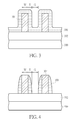
Then, as shown in FIG. 3 , a material layer 306, such as a silicon nitride (SiN) layer, is formed conformally on the sacrificial layer 304. The method of forming the material layer 306 can include a chemical vapor deposition (CVD) process or an atomic layer deposition (ALD) process. In the present embodiment, the thickness of the material layer 306 is adjusted according to the width W of the sacrificial layer 304 obtained in the measuring step. In one embodiment, as shown in FIG. 3 , the thickness T of the material layer 306 is adjusted so that a gap G between two facing material layers 306 on the sidewalls of the sacrificial layer 304 is substantially equal to the width W of the sacrificial layer 304.
Then, as shown in FIG. 4 , the material layer 306 is anisotropically removed until a top surface of the sacrificial layer 304 and the mask layer 302 is exposed. The material layer 306 becomes a spacer 308 on the sidewall of the sacrificial layer 304. It is understood that the spacer 308 also has the width W.
As shown in FIG. 5 , the sacrificial layer 304 is completely removed, but the spacer 308 still remains on the mask layer 302. Since the gap G between the material layer 306 is equal to the width W of the sacrificial layer 304, i.e. G=W, so after removing the patterned first material layer 308, the spacing (W and G) between each spacer 308 remains the same.
Then, as shown in FIG. 6 , an isotropic etching process such as a trimming process is performed toward the spacer 308. The sidewall of the spacer 308 is trimmed, for example by using suitable plasma gases to slightly reduce the width of the spacer 308. After the trimming process, the width of the spacer 308 is reduced from T to T′, which is the final desired critical dimension (CD) of the pattern. Since the spacing between each spacer 308 is equal, so even after the trimming process that isotropically removes the spacer 308 along the horizontal direction, the spacing between each spacer 308 is still the same and no shifting problem would occur in the present invention. In the present embodiment, the trimming time can also be adjusted according to the measured results of the sacrificial layer width W. The thicker the material layer 306 is, the longer trimming time will be required in the process, in order to achieve the correct final pattern spacing and CD.
As shown in FIG. 7 , an etching process is performed by using the trimmed spacer 308 as a mask to pattern the mask layer 302, thereby forming a patterned mask layer 303. Consequently, the pattern of the spacer 308 with a desired width T′ is transferred to the mask layer 303. Thereafter, the pattern of the patterned mask layer 303 can be further transferred to the substrate 300 to form a desired semiconductor structure in the substrate 300, such as a fin structure of a Fin-FET, or a word line of a dynamic random access memory (DRAM), and is not limited thereto. In one embodiment, after forming the patterned mask layer 303, the patterned mask layer 303 can undergo a trimming process again, in which the time of the trimming process can be adjusted according to the measured result of the width W of the sacrificial layer 304. In another embodiment, the mask layer 302 can be omitted so the pattern of the spacer 308 can be directly transferred to the substrate 300.
In the abovementioned embodiment, a measuring step is performed to measure the width W of the sacrificial layer 304 in-situ, so that, in the subsequent step, the thickness of the material layer 306 can be decided, and the trimming process toward the spacer 308 can be adjusted, wherein both of these processes are based on the measured result of the actual width W of the sacrificial layer 304. By doing this, the spacings between every spacer 308 can be equal to each others and a correct final pattern spacing and CD can be obtained. In addition, since the width of the pattern can be adjusted in the final trimming step, the original width W of the sacrificial layer 304 can be designed to be smaller than that in conventional arts, thereby giving more margins to the manufacturing processes.
Please refer to FIG. 8 to FIG. 9 , which are schematic diagrams of the SIT process according to the second embodiment of the present invention. The previous steps in the second embodiment are similar to those in the first embodiment as in FIG. 1 to FIG. 2 . After the steps in FIG. 1 and FIG. 2 , please see FIG. 8 . A material layer 306 is formed conformally on the sacrificial layer 304. Compared with the first embodiment that measures the width of the sacrificial layer 304 and forms the material layer 306 based on the measured result, the second embodiment measures the thickness of the material layer 306 instead of the width of the sacrificial layer 304. That is, a measuring step is performed to measure the actual thickness T of the material layer 306 in-situ to obtain the actual thickness thereof.
The second material layer 308 is then removed anisotropically to form a spacer 308, as shown in FIG. 4 of the first embodiment. As shown in FIG. 9 , an isotropic etching process such as a trimming process is then performed to slightly reduce the width of the spacer 308. In the present embodiment, the trimming process is performed according to the measured result of the thickness of the material layer 306. After the trimming process, the width of the spacer 308 has the desired value. Then, the sacrificial layer 304 is removed and the pattern of the spacer 308 can be transferred to the mask layer 302, as shown in FIG. 7 of the first embodiment.
In the second embodiment, a measuring step is used to measure the thickness of the second material layer 308 and the thickness thereof can be slightly adjusted in the trimming process. It is noted the second embodiment focuses on the thickness of the second material 306 (which will become the spacer 308), so the trimming process is performed before removing the sacrificial layer 304. By doing this, the trimming process in the second embodiment can directly compensate the thickness of the material layer 306. On the other hand, the trimming process in the first embodiment focuses both on the spacing between each spacer 308 and the final CD of the spacer 308, so it is performed after removing the sacrificial layer 304 and is based on the width W of the sacrificial layer 304 and/or the thickness of the material layer 306.
In another embodiment, the first embodiment and the second embodiment can be incorporated. Please refer to FIG. 10 , which shows a flow chart of the SIT process in the present invention. The process includes the following steps in sequence:
Step 400: providing a substrate.
Step 402: forming a sacrificial layer on the substrate.
Step 406: forming a material layer conformally on the sacrificial layer.
Step 410: performing an anisotropic process to make the material layer become a spacer.
Step 412: performing a first trimming process toward the spacer.
Step 414: removing the sacrificial layer.
Step 416: performing a second trimming process toward the spacer.
In one embodiment, after the sacrificial layer is formed, a width of the sacrificial layer is measured (step 404). The thickness of the second material layer is determined by the result measured in step 404 (step 418). The time of the second trimming process in step 416 is adjusted according to the result measured in step 404 (step 422). Thus, the automatic process control ability can be achieved by the measuring step in step 404 and the adjusting steps in step 418 and/or step 422.
In another embodiment, after the material layer is formed, a thickness of the material layer is measured (step 408). The time of the first trimming process in step 412 is adjusted according to the result measured in step 408 (step 420). Thus, the automatic processing control ability can be provided by the measuring step in step 408 and the adjusting step in step 420.
In summary, the present invention provides a sidewall image transfer process that has an APC ability to ensure that the CD of the final pattern and the space between each pattern correspond to the target. The APC ability is achieved by using at least a measuring step to detect in-situ the width of the sacrificial layer and/or the thickness of the material layer, so that the subsequent adjusting steps can adjust the thickness of the material layer or the trimming time according to the measured results.
Those skilled in the art will readily observe that numerous modifications and alterations of the device and method may be made while retaining the teachings of the invention. Accordingly, the above disclosure should be construed as limited only by the metes and bounds of the appended claims.
Claims (12)
1. A sidewall image transfer process, comprising:
providing a substrate;
forming a sacrificial layer having a pattern on the substrate;
performing a first measuring step to measure a width of the pattern of the sacrificial layer;
forming a material layer conformally on the sacrificial layer, wherein a thickness of the material layer is adjusted according to a result of the first measuring step;
performing a second measuring step to measure a thickness of the material layer;
removing the material layer anisotropically after performing the second measuring step, so the material layer becomes a spacer on a sidewall of the sacrificial layer;
performing a first trimming process toward the spacer, wherein the trimming time of the first trimming process is adjusted according to a result of the second measuring step, the first trimming process performed toward the spacer reduces a width of the spacer, and the width of the spacer after the first trimming process is less than the thickness of the material layer; and
removing the sacrificial layer after the first trimming process.
2. The sidewall image transfer process according to claim 1 , wherein the thickness of the material layer is adjusted to have a gap width of a gap between two facing material layers on the sidewalls of the sacrificial layer equal to a width of the sacrificial layer.
3. The sidewall image transfer process according to claim 1 , further comprising performing a second trimming process toward the spacer after removing the sacrificial layer.
4. The sidewall image transfer process according to claim 3 , wherein the trimming time of the second trimming process is adjusted based on the thickness of the material layer measured in the second measuring step so as to control a spacing of the spacer.
5. The sidewall image transfer process according to claim 1 , wherein the sacrificial layer comprises poly-silicon or amorphous silicon.
6. The sidewall image transfer process according to claim 1 , wherein the material layer comprises silicon nitride.
7. The sidewall image transfer process according to claim 1 , further comprising forming a mask layer on the substrate before forming the material layer.
8. The sidewall image transfer process according to claim 7 , further comprising patterning the mask layer by using the spacer as a mask after removing the sacrificial layer.
9. The sidewall image transfer process according to claim 1 , wherein the sacrificial layer is partially uncovered by the material layer after the step of removing the material layer anisotropically, and the first trimming process is performed after the spacer is formed and the sacrificial layer is partially uncovered by the material layer.
10. The sidewall image transfer process according to claim 1 , wherein a width of the pattern of the sacrificial layer is unchanged after the step of forming the material layer.
11. The sidewall image transfer process according to claim 1 , wherein the thickness of the material layer is adjusted based on the width of the pattern of the sacrificial layer during the step of forming a material layer conformally on the sacrificial layer.
12. The sidewall image transfer process according to claim 3 , further comprising performing a second trimming process toward the spacer after the step of removing the sacrificial layer so as to control a spacing of the spacer, wherein a trimming time of the second trimming process is adjusted based on a width of the pattern of the sacrificial layer.
Priority Applications (1)
| Application Number | Priority Date | Filing Date | Title |
|---|---|---|---|
| US13/862,484 US9711368B2 (en) | 2013-04-15 | 2013-04-15 | Sidewall image transfer process |
Applications Claiming Priority (1)
| Application Number | Priority Date | Filing Date | Title |
|---|---|---|---|
| US13/862,484 US9711368B2 (en) | 2013-04-15 | 2013-04-15 | Sidewall image transfer process |
Publications (2)
| Publication Number | Publication Date |
|---|---|
| US20140308761A1 US20140308761A1 (en) | 2014-10-16 |
| US9711368B2 true US9711368B2 (en) | 2017-07-18 |
Family
ID=51687068
Family Applications (1)
| Application Number | Title | Priority Date | Filing Date |
|---|---|---|---|
| US13/862,484 Active 2033-11-11 US9711368B2 (en) | 2013-04-15 | 2013-04-15 | Sidewall image transfer process |
Country Status (1)
| Country | Link |
|---|---|
| US (1) | US9711368B2 (en) |
Families Citing this family (7)
| Publication number | Priority date | Publication date | Assignee | Title |
|---|---|---|---|---|
| US9263282B2 (en) * | 2013-06-13 | 2016-02-16 | United Microelectronics Corporation | Method of fabricating semiconductor patterns |
| US9177875B2 (en) * | 2013-11-15 | 2015-11-03 | Taiwan Seminconductor Manufacturing Co., Ltd. | Advanced process control method for controlling width of spacer and dummy sidewall in semiconductor device |
| KR102449901B1 (en) * | 2015-06-23 | 2022-09-30 | 삼성전자주식회사 | Integrated circuit device and method of manufacturing the same |
| US10157742B2 (en) | 2015-12-31 | 2018-12-18 | Taiwan Semiconductor Manufacturing Co., Ltd. | Method for mandrel and spacer patterning |
| CN109494149B (en) * | 2017-09-13 | 2020-10-23 | 联华电子股份有限公司 | Method for manufacturing semiconductor structure |
| US10396084B1 (en) | 2018-04-04 | 2019-08-27 | Globalfoundries Inc. | Semiconductor devices including self-aligned active regions for planar transistor architecture |
| CN113506728A (en) * | 2021-06-29 | 2021-10-15 | 长江存储科技有限责任公司 | Manufacturing method of semiconductor structure and semiconductor structure |
Citations (90)
| Publication number | Priority date | Publication date | Assignee | Title |
|---|---|---|---|---|
| US4776922A (en) * | 1987-10-30 | 1988-10-11 | International Business Machines Corporation | Formation of variable-width sidewall structures |
| US6043138A (en) | 1996-09-16 | 2000-03-28 | Advanced Micro Devices, Inc. | Multi-step polysilicon deposition process for boron penetration inhibition |
| US6409879B1 (en) * | 2000-01-20 | 2002-06-25 | Advanced Micro Devices, Inc. | System for controlling transistor spacer width |
| US6492216B1 (en) | 2002-02-07 | 2002-12-10 | Taiwan Semiconductor Manufacturing Company | Method of forming a transistor with a strained channel |
| US20030157436A1 (en) * | 2002-02-20 | 2003-08-21 | Dirk Manger | Method for forming a hard mask in a layer on a planar device |
| US6617258B1 (en) * | 2001-07-23 | 2003-09-09 | Advanced Micro Devices, Inc. | Method of forming a gate insulation layer for a semiconductor device by controlling the duration of an etch process, and system for accomplishing same |
| US6632741B1 (en) * | 2000-07-19 | 2003-10-14 | International Business Machines Corporation | Self-trimming method on looped patterns |
| US20040084674A1 (en) * | 2002-10-31 | 2004-05-06 | Leo Mathew | Multiple gate transistor employing monocrystalline silicon walls |
| US20040195624A1 (en) | 2003-04-04 | 2004-10-07 | National Taiwan University | Strained silicon fin field effect transistor |
| US20050051825A1 (en) | 2003-09-09 | 2005-03-10 | Makoto Fujiwara | Semiconductor device and manufacturing method thereof |
| US6875703B1 (en) * | 2004-01-20 | 2005-04-05 | International Business Machines Corporation | Method for forming quadruple density sidewall image transfer (SIT) structures |
| US6921963B2 (en) | 2003-01-23 | 2005-07-26 | Advanced Micro Devices, Inc | Narrow fin FinFET |
| US20060099830A1 (en) | 2004-11-05 | 2006-05-11 | Varian Semiconductor Equipment Associates, Inc. | Plasma implantation using halogenated dopant species to limit deposition of surface layers |
| US7087477B2 (en) | 2001-12-04 | 2006-08-08 | International Business Machines Corporation | FinFET SRAM cell using low mobility plane for cell stability and method for forming |
| US7091551B1 (en) | 2005-04-13 | 2006-08-15 | International Business Machines Corporation | Four-bit FinFET NVRAM memory device |
| US7102181B1 (en) * | 2005-04-22 | 2006-09-05 | International Business Machines Corporation | Structure and method for dual-gate FET with SOI substrate |
| US20060273456A1 (en) * | 2005-06-02 | 2006-12-07 | Micron Technology, Inc., A Corporation | Multiple spacer steps for pitch multiplication |
| US20060281266A1 (en) * | 2005-06-09 | 2006-12-14 | Wells David H | Method and apparatus for adjusting feature size and position |
| US20060286729A1 (en) | 2005-06-21 | 2006-12-21 | Jack Kavalieros | Complementary metal oxide semiconductor integrated circuit using raised source drain and replacement metal gate |
| US20070026684A1 (en) * | 2005-08-01 | 2007-02-01 | Stefano Parascandola | Method of producing pitch fractionizations in semiconductor technology |
| US20070049040A1 (en) * | 2005-03-15 | 2007-03-01 | Micron Technology, Inc., A Corporation | Multiple deposition for integration of spacers in pitch multiplication process |
| US20070108528A1 (en) | 2005-11-15 | 2007-05-17 | International Business Machines Corporation | Sram cell |
| US20070158756A1 (en) | 2006-01-12 | 2007-07-12 | Lars Dreeskornfeld | Production method for a FinFET transistor arrangement, and corresponding FinFET transistor arrangement |
| US7247887B2 (en) | 2005-07-01 | 2007-07-24 | Synopsys, Inc. | Segmented channel MOS transistor |
| US20070170521A1 (en) * | 2006-01-12 | 2007-07-26 | International Business Machines Corporation | Method and structure to process thick and thin fins and variable fin to fin spacing |
| US7250658B2 (en) | 2003-06-26 | 2007-07-31 | International Business Machines Corporation | Hybrid planar and FinFET CMOS devices |
| US20070284669A1 (en) * | 2004-05-25 | 2007-12-13 | Abadeer Wagdi W | Method and structure to process thick and thin fins and variable fin to fin spacing |
| US7309626B2 (en) | 2005-11-15 | 2007-12-18 | International Business Machines Corporation | Quasi self-aligned source/drain FinFET process |
| US7327476B2 (en) * | 2002-06-26 | 2008-02-05 | Nova Measuring Instruments Ltd. | Thin films measurement method and system |
| US7348192B2 (en) * | 2003-09-05 | 2008-03-25 | Kabushiki Kaisha Toshiba | Method for monitoring film thickness, a system for monitoring film thickness, a method for manufacturing a semiconductor device, and a program product for controlling film thickness monitoring system |
| US7352034B2 (en) | 2005-08-25 | 2008-04-01 | International Business Machines Corporation | Semiconductor structures integrating damascene-body FinFET's and planar devices on a common substrate and methods for forming such semiconductor structures |
| US7390750B1 (en) * | 2004-03-23 | 2008-06-24 | Cypress Semiconductor Corp. | Method of patterning elements within a semiconductor topography |
| US20080157208A1 (en) | 2006-12-29 | 2008-07-03 | Fischer Kevin J | Stressed barrier plug slot contact structure for transistor performance enhancement |
| US20080197394A1 (en) * | 2007-02-20 | 2008-08-21 | Qimonda Ag | Methods of manufacturing semiconductor structures |
| US7416937B2 (en) * | 2003-12-30 | 2008-08-26 | Dongbu Electronics Co., Ltd. | Semiconductor device and method for fabricating the same |
| US20080296732A1 (en) * | 2007-05-31 | 2008-12-04 | Micron Technology, Inc. | Methods of isolating array features during pitch doubling processes and semiconductor device structures having isolated array features |
| US7470570B2 (en) | 2006-11-14 | 2008-12-30 | International Business Machines Corporation | Process for fabrication of FinFETs |
| US7531437B2 (en) | 2004-09-30 | 2009-05-12 | Intel Corporation | Method of forming metal gate electrodes using sacrificial gate electrode material and sacrificial gate dielectric material |
| US20090124097A1 (en) | 2007-11-09 | 2009-05-14 | International Business Machines Corporation | Method of forming narrow fins in finfet devices with reduced spacing therebetween |
| US7569857B2 (en) | 2006-09-29 | 2009-08-04 | Intel Corporation | Dual crystal orientation circuit devices on the same substrate |
| US20090242964A1 (en) | 2006-04-26 | 2009-10-01 | Nxp B.V. | Non-volatile memory device |
| US20090269916A1 (en) | 2008-04-28 | 2009-10-29 | Inkuk Kang | Methods for fabricating memory cells having fin structures with semicircular top surfaces and rounded top corners and edges |
| US20100022033A1 (en) * | 2006-03-28 | 2010-01-28 | Lam Research Corporation | Process for wafer temperature verification in etch tools |
| US20100048027A1 (en) | 2008-08-21 | 2010-02-25 | International Business Machines Corporation | Smooth and vertical semiconductor fin structure |
| US20100072553A1 (en) | 2008-09-23 | 2010-03-25 | Taiwan Semiconductor Manufacturing Co., Ltd. | METAL GATE STRESS FILM FOR MOBILITY ENHANCEMENT IN FinFET DEVICE |
| US7687339B1 (en) * | 2009-02-04 | 2010-03-30 | Advanced Micro Devices, Inc. | Methods for fabricating FinFET structures having different channel lengths |
| US20100144121A1 (en) | 2008-12-05 | 2010-06-10 | Cheng-Hung Chang | Germanium FinFETs Having Dielectric Punch-Through Stoppers |
| US20100167506A1 (en) | 2008-12-31 | 2010-07-01 | Taiwan Semiconductor Manufacturing Co., Ltd. | Inductive plasma doping |
| US20100197096A1 (en) * | 2009-02-04 | 2010-08-05 | Advanced Micro Devices, Inc. | Methods for fabricating finfet structures having different channel lengths |
| US20100248481A1 (en) * | 2009-03-27 | 2010-09-30 | Schultz Richard T | Cad flow for 15nm/22nm multiple fine grained wimpy gate lengths in sit gate flow |
| US20100267238A1 (en) * | 2009-04-20 | 2010-10-21 | Advanced Micro Devices, Inc. | Methods for fabricating finfet semiconductor devices using planarized spacers |
| US20100267237A1 (en) * | 2009-04-20 | 2010-10-21 | Advanced Micro Devices, Inc. | Methods for fabricating finfet semiconductor devices using ashable sacrificial mandrels |
| US20110021026A1 (en) * | 2009-07-27 | 2011-01-27 | Globalfoundries Inc. | Methods for fabricating finfet semiconductor devices using l-shaped spacers |
| US20110021010A1 (en) * | 2009-07-27 | 2011-01-27 | International Business Machines Corporation | Method for double pattern density |
| US20110053361A1 (en) * | 2009-09-02 | 2011-03-03 | Ramachandran Muralidhar | FinFET Formation with a Thermal Oxide Spacer Hard Mask Formed from Crystalline Silicon Layer |
| US8232212B2 (en) * | 2008-07-11 | 2012-07-31 | Applied Materials, Inc. | Within-sequence metrology based process tuning for adaptive self-aligned double patterning |
| US20130089984A1 (en) * | 2011-10-06 | 2013-04-11 | International Business Machines Corporation | Sidewall image transfer process with multiple critical dimensions |
| US20130134486A1 (en) * | 2011-11-28 | 2013-05-30 | Globalfoundries Inc. | Methods of Patterning Features in a Structure Using Multiple Sidewall Image Transfer Technique |
| US20130143372A1 (en) * | 2011-12-06 | 2013-06-06 | Samsung Electronics Co., Ltd. | Methods of forming patterns of a semiconductor device |
| US20130196508A1 (en) * | 2012-01-26 | 2013-08-01 | Globalfoundries Inc. | Methods of Forming SRAM Devices Using Sidewall Image Transfer Techniques |
| US20130244437A1 (en) * | 2012-03-15 | 2013-09-19 | Globalfoundries Inc. | Methods of forming features on an integrated circuit product using a novel compound sidewall image transfer technique |
| US8546202B2 (en) * | 2011-11-09 | 2013-10-01 | United Microelectronics Corp. | Manufacturing method for semiconductor structures |
| US20130334602A1 (en) * | 2012-06-14 | 2013-12-19 | International Business Machines Corporation | Continuously scalable width and height semiconductor fins |
| US20140159164A1 (en) * | 2012-12-10 | 2014-06-12 | Globalfoundries Inc. | Double sidewall image transfer process |
| US20140203279A1 (en) * | 2013-01-21 | 2014-07-24 | GlobalFoundries, Inc. | Test structure and method to faciltiate development/optimization of process parameters |
| US20140327074A1 (en) * | 2013-05-02 | 2014-11-06 | United Microelectronics Corp. | Semiconductor integrated circuit |
| US20140329388A1 (en) * | 2013-05-01 | 2014-11-06 | International Business Machines Corporation | Methods of patterning features having differing widths |
| US20140339641A1 (en) * | 2013-05-16 | 2014-11-20 | United Microelectronics Corp. | Semiconductor device and fabrication method thereof |
| US8900937B2 (en) * | 2013-03-11 | 2014-12-02 | Taiwan Semiconductor Manufacturing Company, Ltd. | FinFET device structure and methods of making same |
| US8906752B2 (en) * | 2011-09-16 | 2014-12-09 | Kateeva, Inc. | Polythiophene-containing ink compositions for inkjet printing |
| US20140367833A1 (en) * | 2013-06-12 | 2014-12-18 | International Business Machines Corporation | Low-Temperature Sidewall Image Transfer Process Using ALD Metals, Metal Oxides and Metal Nitrides |
| US20150011090A1 (en) * | 2013-07-03 | 2015-01-08 | United Microelectronics Corp. | Fin-shaped structure forming process |
| US20150017781A1 (en) * | 2013-07-12 | 2015-01-15 | United Microelectronics Corp. | Method of forming shallow trench isolation structure |
| US8965551B2 (en) * | 2010-08-20 | 2015-02-24 | Kabushiki Kaisha Toshiba | Defect analyzing method and defect analyzing apparatus |
| US20150056724A1 (en) * | 2013-08-20 | 2015-02-26 | Taiwan Semiconductor Manufacturing Company, Ltd. | Integrated circuit layout and method with double patterning |
| US20150064913A1 (en) * | 2013-09-02 | 2015-03-05 | Kabushiki Kaisha Toshiba | Method of manufacturing a semiconductor device |
| US8975129B1 (en) * | 2013-11-13 | 2015-03-10 | Taiwan Semiconductor Manufacturing Company, Ltd. | Method of making a FinFET device |
| US9006110B1 (en) * | 2013-11-08 | 2015-04-14 | United Microelectronics Corp. | Method for fabricating patterned structure of semiconductor device |
| US9023695B2 (en) * | 2013-03-14 | 2015-05-05 | Taiwan Semiconductor Manufacturing Company, Ltd. | Method of patterning features of a semiconductor device |
| US9029263B1 (en) * | 2013-12-12 | 2015-05-12 | Texas Instruments Incorporated | Method of printing multiple structure widths using spacer double patterning |
| US20150236015A1 (en) * | 2014-02-19 | 2015-08-20 | Yeong-Jong Jeong | Integrated circuit devices with source/drain regions including multiple segments and method of forming the same |
| US20150241785A1 (en) * | 2014-02-21 | 2015-08-27 | Kabushiki Kaisha Toshiba | Method of manufacturing semiconductor device |
| US20150243503A1 (en) * | 2014-02-25 | 2015-08-27 | International Business Machines Corporation | Stacked sidewall patterning |
| US9123776B2 (en) * | 2013-12-04 | 2015-09-01 | Taiwan Semiconductor Manufacturing Company, Ltd. | Self-aligned double spacer patterning process |
| US9153440B2 (en) * | 2012-03-23 | 2015-10-06 | Taiwan Semiconductor Manufacturing Company, Ltd. | Method of forming a semiconductor device |
| US20150287612A1 (en) * | 2014-04-07 | 2015-10-08 | Applied Materials, Inc. | Spacer formation |
| US20150311085A1 (en) * | 2014-04-23 | 2015-10-29 | Globalfoundries Inc. | Field effect transistor (finfet) device with a planar block area to enable varialble fin pitch and width |
| US9177797B2 (en) * | 2013-12-04 | 2015-11-03 | Taiwan Semiconductor Manufacturing Company, Ltd. | Lithography using high selectivity spacers for pitch reduction |
| US20150318181A1 (en) * | 2014-05-02 | 2015-11-05 | GlobalFoundries, Inc. | Methods for fabricating integrated circuits using self-aligned quadruple patterning |
| US9263282B2 (en) * | 2013-06-13 | 2016-02-16 | United Microelectronics Corporation | Method of fabricating semiconductor patterns |
-
2013
- 2013-04-15 US US13/862,484 patent/US9711368B2/en active Active
Patent Citations (97)
| Publication number | Priority date | Publication date | Assignee | Title |
|---|---|---|---|---|
| US4776922A (en) * | 1987-10-30 | 1988-10-11 | International Business Machines Corporation | Formation of variable-width sidewall structures |
| US6043138A (en) | 1996-09-16 | 2000-03-28 | Advanced Micro Devices, Inc. | Multi-step polysilicon deposition process for boron penetration inhibition |
| US6409879B1 (en) * | 2000-01-20 | 2002-06-25 | Advanced Micro Devices, Inc. | System for controlling transistor spacer width |
| US6632741B1 (en) * | 2000-07-19 | 2003-10-14 | International Business Machines Corporation | Self-trimming method on looped patterns |
| US6617258B1 (en) * | 2001-07-23 | 2003-09-09 | Advanced Micro Devices, Inc. | Method of forming a gate insulation layer for a semiconductor device by controlling the duration of an etch process, and system for accomplishing same |
| US7087477B2 (en) | 2001-12-04 | 2006-08-08 | International Business Machines Corporation | FinFET SRAM cell using low mobility plane for cell stability and method for forming |
| US6492216B1 (en) | 2002-02-07 | 2002-12-10 | Taiwan Semiconductor Manufacturing Company | Method of forming a transistor with a strained channel |
| US20030157436A1 (en) * | 2002-02-20 | 2003-08-21 | Dirk Manger | Method for forming a hard mask in a layer on a planar device |
| US7327476B2 (en) * | 2002-06-26 | 2008-02-05 | Nova Measuring Instruments Ltd. | Thin films measurement method and system |
| US20040084674A1 (en) * | 2002-10-31 | 2004-05-06 | Leo Mathew | Multiple gate transistor employing monocrystalline silicon walls |
| US6921963B2 (en) | 2003-01-23 | 2005-07-26 | Advanced Micro Devices, Inc | Narrow fin FinFET |
| US20040195624A1 (en) | 2003-04-04 | 2004-10-07 | National Taiwan University | Strained silicon fin field effect transistor |
| US7250658B2 (en) | 2003-06-26 | 2007-07-31 | International Business Machines Corporation | Hybrid planar and FinFET CMOS devices |
| US7348192B2 (en) * | 2003-09-05 | 2008-03-25 | Kabushiki Kaisha Toshiba | Method for monitoring film thickness, a system for monitoring film thickness, a method for manufacturing a semiconductor device, and a program product for controlling film thickness monitoring system |
| US20050051825A1 (en) | 2003-09-09 | 2005-03-10 | Makoto Fujiwara | Semiconductor device and manufacturing method thereof |
| US7416937B2 (en) * | 2003-12-30 | 2008-08-26 | Dongbu Electronics Co., Ltd. | Semiconductor device and method for fabricating the same |
| US6875703B1 (en) * | 2004-01-20 | 2005-04-05 | International Business Machines Corporation | Method for forming quadruple density sidewall image transfer (SIT) structures |
| US7390750B1 (en) * | 2004-03-23 | 2008-06-24 | Cypress Semiconductor Corp. | Method of patterning elements within a semiconductor topography |
| US20070284669A1 (en) * | 2004-05-25 | 2007-12-13 | Abadeer Wagdi W | Method and structure to process thick and thin fins and variable fin to fin spacing |
| US7531437B2 (en) | 2004-09-30 | 2009-05-12 | Intel Corporation | Method of forming metal gate electrodes using sacrificial gate electrode material and sacrificial gate dielectric material |
| US20060099830A1 (en) | 2004-11-05 | 2006-05-11 | Varian Semiconductor Equipment Associates, Inc. | Plasma implantation using halogenated dopant species to limit deposition of surface layers |
| US20070049040A1 (en) * | 2005-03-15 | 2007-03-01 | Micron Technology, Inc., A Corporation | Multiple deposition for integration of spacers in pitch multiplication process |
| US7091551B1 (en) | 2005-04-13 | 2006-08-15 | International Business Machines Corporation | Four-bit FinFET NVRAM memory device |
| US7102181B1 (en) * | 2005-04-22 | 2006-09-05 | International Business Machines Corporation | Structure and method for dual-gate FET with SOI substrate |
| US20060273456A1 (en) * | 2005-06-02 | 2006-12-07 | Micron Technology, Inc., A Corporation | Multiple spacer steps for pitch multiplication |
| US20060281266A1 (en) * | 2005-06-09 | 2006-12-14 | Wells David H | Method and apparatus for adjusting feature size and position |
| US20060286729A1 (en) | 2005-06-21 | 2006-12-21 | Jack Kavalieros | Complementary metal oxide semiconductor integrated circuit using raised source drain and replacement metal gate |
| US7247887B2 (en) | 2005-07-01 | 2007-07-24 | Synopsys, Inc. | Segmented channel MOS transistor |
| US20070026684A1 (en) * | 2005-08-01 | 2007-02-01 | Stefano Parascandola | Method of producing pitch fractionizations in semiconductor technology |
| US7352034B2 (en) | 2005-08-25 | 2008-04-01 | International Business Machines Corporation | Semiconductor structures integrating damascene-body FinFET's and planar devices on a common substrate and methods for forming such semiconductor structures |
| US7309626B2 (en) | 2005-11-15 | 2007-12-18 | International Business Machines Corporation | Quasi self-aligned source/drain FinFET process |
| US20070108528A1 (en) | 2005-11-15 | 2007-05-17 | International Business Machines Corporation | Sram cell |
| US20070170521A1 (en) * | 2006-01-12 | 2007-07-26 | International Business Machines Corporation | Method and structure to process thick and thin fins and variable fin to fin spacing |
| US20070158756A1 (en) | 2006-01-12 | 2007-07-12 | Lars Dreeskornfeld | Production method for a FinFET transistor arrangement, and corresponding FinFET transistor arrangement |
| US20100022033A1 (en) * | 2006-03-28 | 2010-01-28 | Lam Research Corporation | Process for wafer temperature verification in etch tools |
| US20090242964A1 (en) | 2006-04-26 | 2009-10-01 | Nxp B.V. | Non-volatile memory device |
| US7569857B2 (en) | 2006-09-29 | 2009-08-04 | Intel Corporation | Dual crystal orientation circuit devices on the same substrate |
| US7470570B2 (en) | 2006-11-14 | 2008-12-30 | International Business Machines Corporation | Process for fabrication of FinFETs |
| US20090101995A1 (en) * | 2006-11-14 | 2009-04-23 | International Business Machines Corporation | PROCESS FOR FABRICATION OF FINFETs |
| US20080157208A1 (en) | 2006-12-29 | 2008-07-03 | Fischer Kevin J | Stressed barrier plug slot contact structure for transistor performance enhancement |
| US20080197394A1 (en) * | 2007-02-20 | 2008-08-21 | Qimonda Ag | Methods of manufacturing semiconductor structures |
| US20080296732A1 (en) * | 2007-05-31 | 2008-12-04 | Micron Technology, Inc. | Methods of isolating array features during pitch doubling processes and semiconductor device structures having isolated array features |
| US20090124097A1 (en) | 2007-11-09 | 2009-05-14 | International Business Machines Corporation | Method of forming narrow fins in finfet devices with reduced spacing therebetween |
| US20090269916A1 (en) | 2008-04-28 | 2009-10-29 | Inkuk Kang | Methods for fabricating memory cells having fin structures with semicircular top surfaces and rounded top corners and edges |
| US8232212B2 (en) * | 2008-07-11 | 2012-07-31 | Applied Materials, Inc. | Within-sequence metrology based process tuning for adaptive self-aligned double patterning |
| US20100048027A1 (en) | 2008-08-21 | 2010-02-25 | International Business Machines Corporation | Smooth and vertical semiconductor fin structure |
| US20100072553A1 (en) | 2008-09-23 | 2010-03-25 | Taiwan Semiconductor Manufacturing Co., Ltd. | METAL GATE STRESS FILM FOR MOBILITY ENHANCEMENT IN FinFET DEVICE |
| US20100144121A1 (en) | 2008-12-05 | 2010-06-10 | Cheng-Hung Chang | Germanium FinFETs Having Dielectric Punch-Through Stoppers |
| US20100167506A1 (en) | 2008-12-31 | 2010-07-01 | Taiwan Semiconductor Manufacturing Co., Ltd. | Inductive plasma doping |
| US7687339B1 (en) * | 2009-02-04 | 2010-03-30 | Advanced Micro Devices, Inc. | Methods for fabricating FinFET structures having different channel lengths |
| US20110014791A1 (en) * | 2009-02-04 | 2011-01-20 | Globalfoundries Inc. | Methods for fabricating finfet structures having different channel lengths |
| US20100197096A1 (en) * | 2009-02-04 | 2010-08-05 | Advanced Micro Devices, Inc. | Methods for fabricating finfet structures having different channel lengths |
| US20100248481A1 (en) * | 2009-03-27 | 2010-09-30 | Schultz Richard T | Cad flow for 15nm/22nm multiple fine grained wimpy gate lengths in sit gate flow |
| US20100267238A1 (en) * | 2009-04-20 | 2010-10-21 | Advanced Micro Devices, Inc. | Methods for fabricating finfet semiconductor devices using planarized spacers |
| US20100267237A1 (en) * | 2009-04-20 | 2010-10-21 | Advanced Micro Devices, Inc. | Methods for fabricating finfet semiconductor devices using ashable sacrificial mandrels |
| US20110021026A1 (en) * | 2009-07-27 | 2011-01-27 | Globalfoundries Inc. | Methods for fabricating finfet semiconductor devices using l-shaped spacers |
| US20110021010A1 (en) * | 2009-07-27 | 2011-01-27 | International Business Machines Corporation | Method for double pattern density |
| US20110053361A1 (en) * | 2009-09-02 | 2011-03-03 | Ramachandran Muralidhar | FinFET Formation with a Thermal Oxide Spacer Hard Mask Formed from Crystalline Silicon Layer |
| US8965551B2 (en) * | 2010-08-20 | 2015-02-24 | Kabushiki Kaisha Toshiba | Defect analyzing method and defect analyzing apparatus |
| US8906752B2 (en) * | 2011-09-16 | 2014-12-09 | Kateeva, Inc. | Polythiophene-containing ink compositions for inkjet printing |
| US20130089984A1 (en) * | 2011-10-06 | 2013-04-11 | International Business Machines Corporation | Sidewall image transfer process with multiple critical dimensions |
| US8546202B2 (en) * | 2011-11-09 | 2013-10-01 | United Microelectronics Corp. | Manufacturing method for semiconductor structures |
| US20130134486A1 (en) * | 2011-11-28 | 2013-05-30 | Globalfoundries Inc. | Methods of Patterning Features in a Structure Using Multiple Sidewall Image Transfer Technique |
| US20130143372A1 (en) * | 2011-12-06 | 2013-06-06 | Samsung Electronics Co., Ltd. | Methods of forming patterns of a semiconductor device |
| US8906757B2 (en) * | 2011-12-06 | 2014-12-09 | Samsung Electronics Co., Ltd. | Methods of forming patterns of a semiconductor device |
| US20130196508A1 (en) * | 2012-01-26 | 2013-08-01 | Globalfoundries Inc. | Methods of Forming SRAM Devices Using Sidewall Image Transfer Techniques |
| US20130244437A1 (en) * | 2012-03-15 | 2013-09-19 | Globalfoundries Inc. | Methods of forming features on an integrated circuit product using a novel compound sidewall image transfer technique |
| US9153440B2 (en) * | 2012-03-23 | 2015-10-06 | Taiwan Semiconductor Manufacturing Company, Ltd. | Method of forming a semiconductor device |
| US20130334602A1 (en) * | 2012-06-14 | 2013-12-19 | International Business Machines Corporation | Continuously scalable width and height semiconductor fins |
| US8927432B2 (en) * | 2012-06-14 | 2015-01-06 | International Business Machines Corporation | Continuously scalable width and height semiconductor fins |
| US8889561B2 (en) * | 2012-12-10 | 2014-11-18 | Globalfoundries Inc. | Double sidewall image transfer process |
| US20140159164A1 (en) * | 2012-12-10 | 2014-06-12 | Globalfoundries Inc. | Double sidewall image transfer process |
| US20140203279A1 (en) * | 2013-01-21 | 2014-07-24 | GlobalFoundries, Inc. | Test structure and method to faciltiate development/optimization of process parameters |
| US8900937B2 (en) * | 2013-03-11 | 2014-12-02 | Taiwan Semiconductor Manufacturing Company, Ltd. | FinFET device structure and methods of making same |
| US9023695B2 (en) * | 2013-03-14 | 2015-05-05 | Taiwan Semiconductor Manufacturing Company, Ltd. | Method of patterning features of a semiconductor device |
| US20140329388A1 (en) * | 2013-05-01 | 2014-11-06 | International Business Machines Corporation | Methods of patterning features having differing widths |
| US20140327074A1 (en) * | 2013-05-02 | 2014-11-06 | United Microelectronics Corp. | Semiconductor integrated circuit |
| US20140339641A1 (en) * | 2013-05-16 | 2014-11-20 | United Microelectronics Corp. | Semiconductor device and fabrication method thereof |
| US20140367833A1 (en) * | 2013-06-12 | 2014-12-18 | International Business Machines Corporation | Low-Temperature Sidewall Image Transfer Process Using ALD Metals, Metal Oxides and Metal Nitrides |
| US9263282B2 (en) * | 2013-06-13 | 2016-02-16 | United Microelectronics Corporation | Method of fabricating semiconductor patterns |
| US20150011090A1 (en) * | 2013-07-03 | 2015-01-08 | United Microelectronics Corp. | Fin-shaped structure forming process |
| US20150017781A1 (en) * | 2013-07-12 | 2015-01-15 | United Microelectronics Corp. | Method of forming shallow trench isolation structure |
| US20150056724A1 (en) * | 2013-08-20 | 2015-02-26 | Taiwan Semiconductor Manufacturing Company, Ltd. | Integrated circuit layout and method with double patterning |
| US20150064913A1 (en) * | 2013-09-02 | 2015-03-05 | Kabushiki Kaisha Toshiba | Method of manufacturing a semiconductor device |
| US9006110B1 (en) * | 2013-11-08 | 2015-04-14 | United Microelectronics Corp. | Method for fabricating patterned structure of semiconductor device |
| US8975129B1 (en) * | 2013-11-13 | 2015-03-10 | Taiwan Semiconductor Manufacturing Company, Ltd. | Method of making a FinFET device |
| US9123776B2 (en) * | 2013-12-04 | 2015-09-01 | Taiwan Semiconductor Manufacturing Company, Ltd. | Self-aligned double spacer patterning process |
| US9177797B2 (en) * | 2013-12-04 | 2015-11-03 | Taiwan Semiconductor Manufacturing Company, Ltd. | Lithography using high selectivity spacers for pitch reduction |
| US9029263B1 (en) * | 2013-12-12 | 2015-05-12 | Texas Instruments Incorporated | Method of printing multiple structure widths using spacer double patterning |
| US20150236015A1 (en) * | 2014-02-19 | 2015-08-20 | Yeong-Jong Jeong | Integrated circuit devices with source/drain regions including multiple segments and method of forming the same |
| US20150241785A1 (en) * | 2014-02-21 | 2015-08-27 | Kabushiki Kaisha Toshiba | Method of manufacturing semiconductor device |
| US9196485B2 (en) * | 2014-02-25 | 2015-11-24 | International Business Machines Corporation | Stacked sidewall patterning |
| US20150243503A1 (en) * | 2014-02-25 | 2015-08-27 | International Business Machines Corporation | Stacked sidewall patterning |
| US20150287612A1 (en) * | 2014-04-07 | 2015-10-08 | Applied Materials, Inc. | Spacer formation |
| US20150311085A1 (en) * | 2014-04-23 | 2015-10-29 | Globalfoundries Inc. | Field effect transistor (finfet) device with a planar block area to enable varialble fin pitch and width |
| US20150318181A1 (en) * | 2014-05-02 | 2015-11-05 | GlobalFoundries, Inc. | Methods for fabricating integrated circuits using self-aligned quadruple patterning |
| US9209038B2 (en) * | 2014-05-02 | 2015-12-08 | GlobalFoundries, Inc. | Methods for fabricating integrated circuits using self-aligned quadruple patterning |
Also Published As
| Publication number | Publication date |
|---|---|
| US20140308761A1 (en) | 2014-10-16 |
Similar Documents
| Publication | Publication Date | Title |
|---|---|---|
| US9711368B2 (en) | Sidewall image transfer process | |
| US9214384B2 (en) | Method of forming trench in semiconductor substrate | |
| US9070635B2 (en) | Removing method | |
| US9006107B2 (en) | Patterned structure of semiconductor device and fabricating method thereof | |
| US8951918B2 (en) | Method for fabricating patterned structure of semiconductor device | |
| US9034762B2 (en) | Triple patterning method | |
| US9129905B2 (en) | Planar metrology pad adjacent a set of fins of a fin field effect transistor device | |
| US11574811B2 (en) | Tight pitch patterning | |
| KR20170046078A (en) | Semiconductor structure and method for forming the same | |
| US10121711B2 (en) | Planar metrology pad adjacent a set of fins of a fin field effect transistor device | |
| US20230207632A1 (en) | Vertical field effect transistor with crosslink fin arrangement | |
| US9208276B1 (en) | Method for generating layout pattern | |
| US9230812B2 (en) | Method for forming semiconductor structure having opening | |
| US9779942B1 (en) | Method of forming patterned mask layer | |
| CN106356303B (en) | Semiconductor device, manufacturing method thereof and electronic device | |
| US10685871B2 (en) | Method for forming semiconductor structure | |
| US8524608B1 (en) | Method for fabricating a patterned structure of a semiconductor device | |
| US20190214273A1 (en) | Method of fabricating semiconductor device | |
| US9502285B1 (en) | Method of forming trenches | |
| EP3101682A1 (en) | Method for providing a patterned target layer in a semiconductor structure | |
| US11482517B2 (en) | Integrated circuit | |
| TWI727049B (en) | Method of manufacturing a semiconductor device | |
| US10090164B2 (en) | Hard masks for block patterning | |
| US20050202680A1 (en) | Method for shrinking a dimension of a gate | |
| US8871649B2 (en) | Methods of forming trench/hole type features in a layer of material of an integrated circuit product |
Legal Events
| Date | Code | Title | Description |
|---|---|---|---|
| AS | Assignment |
Owner name: UNITED MICROELECTRONICS CORP., TAIWAN Free format text: ASSIGNMENT OF ASSIGNORS INTEREST;ASSIGNORS:KUO, LUNG-EN;SU, PO-WEN;WENG, CHEN-YI;AND OTHERS;SIGNING DATES FROM 20130326 TO 20130408;REEL/FRAME:030211/0367 |
|
| STCF | Information on status: patent grant |
Free format text: PATENTED CASE |
|
| MAFP | Maintenance fee payment |
Free format text: PAYMENT OF MAINTENANCE FEE, 4TH YEAR, LARGE ENTITY (ORIGINAL EVENT CODE: M1551); ENTITY STATUS OF PATENT OWNER: LARGE ENTITY Year of fee payment: 4 |