US9673198B2 - Semiconductor devices having active regions at different levels - Google Patents
Semiconductor devices having active regions at different levels Download PDFInfo
- Publication number
- US9673198B2 US9673198B2 US14/682,372 US201514682372A US9673198B2 US 9673198 B2 US9673198 B2 US 9673198B2 US 201514682372 A US201514682372 A US 201514682372A US 9673198 B2 US9673198 B2 US 9673198B2
- Authority
- US
- United States
- Prior art keywords
- fin
- layer
- active region
- device isolation
- region
- Prior art date
- Legal status (The legal status is an assumption and is not a legal conclusion. Google has not performed a legal analysis and makes no representation as to the accuracy of the status listed.)
- Active, expires
Links
- 239000004065 semiconductor Substances 0.000 title claims abstract description 180
- 239000000758 substrate Substances 0.000 claims abstract description 21
- 238000002955 isolation Methods 0.000 claims description 110
- 239000010410 layer Substances 0.000 description 386
- 238000000034 method Methods 0.000 description 66
- 125000006850 spacer group Chemical group 0.000 description 36
- 239000012535 impurity Substances 0.000 description 23
- 229910052581 Si3N4 Inorganic materials 0.000 description 18
- 239000000463 material Substances 0.000 description 18
- HQVNEWCFYHHQES-UHFFFAOYSA-N silicon nitride Chemical compound N12[Si]34N5[Si]62N3[Si]51N64 HQVNEWCFYHHQES-UHFFFAOYSA-N 0.000 description 18
- VYPSYNLAJGMNEJ-UHFFFAOYSA-N Silicium dioxide Chemical compound O=[Si]=O VYPSYNLAJGMNEJ-UHFFFAOYSA-N 0.000 description 17
- 229910052710 silicon Inorganic materials 0.000 description 17
- 229910052814 silicon oxide Inorganic materials 0.000 description 17
- 230000006870 function Effects 0.000 description 15
- 238000005530 etching Methods 0.000 description 14
- 229910000577 Silicon-germanium Inorganic materials 0.000 description 13
- XUIMIQQOPSSXEZ-UHFFFAOYSA-N Silicon Chemical compound [Si] XUIMIQQOPSSXEZ-UHFFFAOYSA-N 0.000 description 12
- 239000010703 silicon Substances 0.000 description 12
- 230000015572 biosynthetic process Effects 0.000 description 10
- 239000013078 crystal Substances 0.000 description 7
- 229910052796 boron Inorganic materials 0.000 description 6
- ZOXJGFHDIHLPTG-UHFFFAOYSA-N Boron Chemical compound [B] ZOXJGFHDIHLPTG-UHFFFAOYSA-N 0.000 description 4
- 229910021419 crystalline silicon Inorganic materials 0.000 description 4
- 108091006146 Channels Proteins 0.000 description 3
- 229910052698 phosphorus Inorganic materials 0.000 description 3
- 229910021420 polycrystalline silicon Inorganic materials 0.000 description 3
- 229920005591 polysilicon Polymers 0.000 description 3
- 239000000126 substance Substances 0.000 description 3
- 108090000699 N-Type Calcium Channels Proteins 0.000 description 2
- 102000004129 N-Type Calcium Channels Human genes 0.000 description 2
- 108010075750 P-Type Calcium Channels Proteins 0.000 description 2
- 238000000231 atomic layer deposition Methods 0.000 description 2
- 230000003247 decreasing effect Effects 0.000 description 2
- 238000010586 diagram Methods 0.000 description 2
- 238000004519 manufacturing process Methods 0.000 description 2
- 239000002184 metal Substances 0.000 description 2
- 229910003465 moissanite Inorganic materials 0.000 description 2
- 238000000059 patterning Methods 0.000 description 2
- 238000000206 photolithography Methods 0.000 description 2
- 238000005498 polishing Methods 0.000 description 2
- 229910010271 silicon carbide Inorganic materials 0.000 description 2
- 238000003860 storage Methods 0.000 description 2
- OKTJSMMVPCPJKN-UHFFFAOYSA-N Carbon Chemical compound [C] OKTJSMMVPCPJKN-UHFFFAOYSA-N 0.000 description 1
- 229910004129 HfSiO Inorganic materials 0.000 description 1
- 229910010038 TiAl Inorganic materials 0.000 description 1
- 229910010041 TiAlC Inorganic materials 0.000 description 1
- ATJFFYVFTNAWJD-UHFFFAOYSA-N Tin Chemical compound [Sn] ATJFFYVFTNAWJD-UHFFFAOYSA-N 0.000 description 1
- 229910052799 carbon Inorganic materials 0.000 description 1
- 238000006243 chemical reaction Methods 0.000 description 1
- 238000005229 chemical vapour deposition Methods 0.000 description 1
- 238000004140 cleaning Methods 0.000 description 1
- 230000009969 flowable effect Effects 0.000 description 1
- 239000012212 insulator Substances 0.000 description 1
- 239000011229 interlayer Substances 0.000 description 1
- 238000012986 modification Methods 0.000 description 1
- 230000004048 modification Effects 0.000 description 1
- 229910021332 silicide Inorganic materials 0.000 description 1
- FVBUAEGBCNSCDD-UHFFFAOYSA-N silicide(4-) Chemical compound [Si-4] FVBUAEGBCNSCDD-UHFFFAOYSA-N 0.000 description 1
Images


Classifications
-
- H—ELECTRICITY
- H01—ELECTRIC ELEMENTS
- H01L—SEMICONDUCTOR DEVICES NOT COVERED BY CLASS H10
- H01L27/00—Devices consisting of a plurality of semiconductor or other solid-state components formed in or on a common substrate
- H01L27/02—Devices consisting of a plurality of semiconductor or other solid-state components formed in or on a common substrate including semiconductor components specially adapted for rectifying, oscillating, amplifying or switching and having at least one potential-jump barrier or surface barrier; including integrated passive circuit elements with at least one potential-jump barrier or surface barrier
- H01L27/04—Devices consisting of a plurality of semiconductor or other solid-state components formed in or on a common substrate including semiconductor components specially adapted for rectifying, oscillating, amplifying or switching and having at least one potential-jump barrier or surface barrier; including integrated passive circuit elements with at least one potential-jump barrier or surface barrier the substrate being a semiconductor body
- H01L27/08—Devices consisting of a plurality of semiconductor or other solid-state components formed in or on a common substrate including semiconductor components specially adapted for rectifying, oscillating, amplifying or switching and having at least one potential-jump barrier or surface barrier; including integrated passive circuit elements with at least one potential-jump barrier or surface barrier the substrate being a semiconductor body including only semiconductor components of a single kind
- H01L27/085—Devices consisting of a plurality of semiconductor or other solid-state components formed in or on a common substrate including semiconductor components specially adapted for rectifying, oscillating, amplifying or switching and having at least one potential-jump barrier or surface barrier; including integrated passive circuit elements with at least one potential-jump barrier or surface barrier the substrate being a semiconductor body including only semiconductor components of a single kind including field-effect components only
- H01L27/088—Devices consisting of a plurality of semiconductor or other solid-state components formed in or on a common substrate including semiconductor components specially adapted for rectifying, oscillating, amplifying or switching and having at least one potential-jump barrier or surface barrier; including integrated passive circuit elements with at least one potential-jump barrier or surface barrier the substrate being a semiconductor body including only semiconductor components of a single kind including field-effect components only the components being field-effect transistors with insulated gate
- H01L27/092—Devices consisting of a plurality of semiconductor or other solid-state components formed in or on a common substrate including semiconductor components specially adapted for rectifying, oscillating, amplifying or switching and having at least one potential-jump barrier or surface barrier; including integrated passive circuit elements with at least one potential-jump barrier or surface barrier the substrate being a semiconductor body including only semiconductor components of a single kind including field-effect components only the components being field-effect transistors with insulated gate complementary MIS field-effect transistors
- H01L27/0924—Devices consisting of a plurality of semiconductor or other solid-state components formed in or on a common substrate including semiconductor components specially adapted for rectifying, oscillating, amplifying or switching and having at least one potential-jump barrier or surface barrier; including integrated passive circuit elements with at least one potential-jump barrier or surface barrier the substrate being a semiconductor body including only semiconductor components of a single kind including field-effect components only the components being field-effect transistors with insulated gate complementary MIS field-effect transistors including transistors with a horizontal current flow in a vertical sidewall of a semiconductor body, e.g. FinFET, MuGFET
-
- H—ELECTRICITY
- H01—ELECTRIC ELEMENTS
- H01L—SEMICONDUCTOR DEVICES NOT COVERED BY CLASS H10
- H01L21/00—Processes or apparatus adapted for the manufacture or treatment of semiconductor or solid state devices or of parts thereof
- H01L21/70—Manufacture or treatment of devices consisting of a plurality of solid state components formed in or on a common substrate or of parts thereof; Manufacture of integrated circuit devices or of parts thereof
- H01L21/77—Manufacture or treatment of devices consisting of a plurality of solid state components or integrated circuits formed in, or on, a common substrate
- H01L21/78—Manufacture or treatment of devices consisting of a plurality of solid state components or integrated circuits formed in, or on, a common substrate with subsequent division of the substrate into plural individual devices
- H01L21/82—Manufacture or treatment of devices consisting of a plurality of solid state components or integrated circuits formed in, or on, a common substrate with subsequent division of the substrate into plural individual devices to produce devices, e.g. integrated circuits, each consisting of a plurality of components
- H01L21/822—Manufacture or treatment of devices consisting of a plurality of solid state components or integrated circuits formed in, or on, a common substrate with subsequent division of the substrate into plural individual devices to produce devices, e.g. integrated circuits, each consisting of a plurality of components the substrate being a semiconductor, using silicon technology
- H01L21/8232—Field-effect technology
- H01L21/8234—MIS technology, i.e. integration processes of field effect transistors of the conductor-insulator-semiconductor type
- H01L21/8238—Complementary field-effect transistors, e.g. CMOS
- H01L21/823821—Complementary field-effect transistors, e.g. CMOS with a particular manufacturing method of transistors with a horizontal current flow in a vertical sidewall of a semiconductor body, e.g. FinFET, MuGFET
-
- H—ELECTRICITY
- H01—ELECTRIC ELEMENTS
- H01L—SEMICONDUCTOR DEVICES NOT COVERED BY CLASS H10
- H01L29/00—Semiconductor devices adapted for rectifying, amplifying, oscillating or switching, or capacitors or resistors with at least one potential-jump barrier or surface barrier, e.g. PN junction depletion layer or carrier concentration layer; Details of semiconductor bodies or of electrodes thereof ; Multistep manufacturing processes therefor
- H01L29/02—Semiconductor bodies ; Multistep manufacturing processes therefor
- H01L29/06—Semiconductor bodies ; Multistep manufacturing processes therefor characterised by their shape; characterised by the shapes, relative sizes, or dispositions of the semiconductor regions ; characterised by the concentration or distribution of impurities within semiconductor regions
- H01L29/0684—Semiconductor bodies ; Multistep manufacturing processes therefor characterised by their shape; characterised by the shapes, relative sizes, or dispositions of the semiconductor regions ; characterised by the concentration or distribution of impurities within semiconductor regions characterised by the shape, relative sizes or dispositions of the semiconductor regions or junctions between the regions
- H01L29/0692—Surface layout
-
- H—ELECTRICITY
- H01—ELECTRIC ELEMENTS
- H01L—SEMICONDUCTOR DEVICES NOT COVERED BY CLASS H10
- H01L29/00—Semiconductor devices adapted for rectifying, amplifying, oscillating or switching, or capacitors or resistors with at least one potential-jump barrier or surface barrier, e.g. PN junction depletion layer or carrier concentration layer; Details of semiconductor bodies or of electrodes thereof ; Multistep manufacturing processes therefor
- H01L29/02—Semiconductor bodies ; Multistep manufacturing processes therefor
- H01L29/06—Semiconductor bodies ; Multistep manufacturing processes therefor characterised by their shape; characterised by the shapes, relative sizes, or dispositions of the semiconductor regions ; characterised by the concentration or distribution of impurities within semiconductor regions
- H01L29/10—Semiconductor bodies ; Multistep manufacturing processes therefor characterised by their shape; characterised by the shapes, relative sizes, or dispositions of the semiconductor regions ; characterised by the concentration or distribution of impurities within semiconductor regions with semiconductor regions connected to an electrode not carrying current to be rectified, amplified or switched and such electrode being part of a semiconductor device which comprises three or more electrodes
- H01L29/1025—Channel region of field-effect devices
- H01L29/1029—Channel region of field-effect devices of field-effect transistors
- H01L29/1033—Channel region of field-effect devices of field-effect transistors with insulated gate, e.g. characterised by the length, the width, the geometric contour or the doping structure
- H01L29/1037—Channel region of field-effect devices of field-effect transistors with insulated gate, e.g. characterised by the length, the width, the geometric contour or the doping structure and non-planar channel
-
- H—ELECTRICITY
- H01—ELECTRIC ELEMENTS
- H01L—SEMICONDUCTOR DEVICES NOT COVERED BY CLASS H10
- H01L29/00—Semiconductor devices adapted for rectifying, amplifying, oscillating or switching, or capacitors or resistors with at least one potential-jump barrier or surface barrier, e.g. PN junction depletion layer or carrier concentration layer; Details of semiconductor bodies or of electrodes thereof ; Multistep manufacturing processes therefor
- H01L29/66—Types of semiconductor device ; Multistep manufacturing processes therefor
- H01L29/68—Types of semiconductor device ; Multistep manufacturing processes therefor controllable by only the electric current supplied, or only the electric potential applied, to an electrode which does not carry the current to be rectified, amplified or switched
- H01L29/76—Unipolar devices, e.g. field effect transistors
- H01L29/772—Field effect transistors
- H01L29/78—Field effect transistors with field effect produced by an insulated gate
- H01L29/785—Field effect transistors with field effect produced by an insulated gate having a channel with a horizontal current flow in a vertical sidewall of a semiconductor body, e.g. FinFET, MuGFET
- H01L29/7853—Field effect transistors with field effect produced by an insulated gate having a channel with a horizontal current flow in a vertical sidewall of a semiconductor body, e.g. FinFET, MuGFET the body having a non-rectangular crossection
- H01L29/7854—Field effect transistors with field effect produced by an insulated gate having a channel with a horizontal current flow in a vertical sidewall of a semiconductor body, e.g. FinFET, MuGFET the body having a non-rectangular crossection with rounded corners
-
- H—ELECTRICITY
- H01—ELECTRIC ELEMENTS
- H01L—SEMICONDUCTOR DEVICES NOT COVERED BY CLASS H10
- H01L21/00—Processes or apparatus adapted for the manufacture or treatment of semiconductor or solid state devices or of parts thereof
- H01L21/70—Manufacture or treatment of devices consisting of a plurality of solid state components formed in or on a common substrate or of parts thereof; Manufacture of integrated circuit devices or of parts thereof
- H01L21/77—Manufacture or treatment of devices consisting of a plurality of solid state components or integrated circuits formed in, or on, a common substrate
- H01L21/78—Manufacture or treatment of devices consisting of a plurality of solid state components or integrated circuits formed in, or on, a common substrate with subsequent division of the substrate into plural individual devices
- H01L21/82—Manufacture or treatment of devices consisting of a plurality of solid state components or integrated circuits formed in, or on, a common substrate with subsequent division of the substrate into plural individual devices to produce devices, e.g. integrated circuits, each consisting of a plurality of components
- H01L21/822—Manufacture or treatment of devices consisting of a plurality of solid state components or integrated circuits formed in, or on, a common substrate with subsequent division of the substrate into plural individual devices to produce devices, e.g. integrated circuits, each consisting of a plurality of components the substrate being a semiconductor, using silicon technology
- H01L21/8232—Field-effect technology
- H01L21/8234—MIS technology, i.e. integration processes of field effect transistors of the conductor-insulator-semiconductor type
- H01L21/823412—MIS technology, i.e. integration processes of field effect transistors of the conductor-insulator-semiconductor type with a particular manufacturing method of the channel structures, e.g. channel implants, halo or pocket implants, or channel materials
-
- H—ELECTRICITY
- H01—ELECTRIC ELEMENTS
- H01L—SEMICONDUCTOR DEVICES NOT COVERED BY CLASS H10
- H01L21/00—Processes or apparatus adapted for the manufacture or treatment of semiconductor or solid state devices or of parts thereof
- H01L21/70—Manufacture or treatment of devices consisting of a plurality of solid state components formed in or on a common substrate or of parts thereof; Manufacture of integrated circuit devices or of parts thereof
- H01L21/77—Manufacture or treatment of devices consisting of a plurality of solid state components or integrated circuits formed in, or on, a common substrate
- H01L21/78—Manufacture or treatment of devices consisting of a plurality of solid state components or integrated circuits formed in, or on, a common substrate with subsequent division of the substrate into plural individual devices
- H01L21/82—Manufacture or treatment of devices consisting of a plurality of solid state components or integrated circuits formed in, or on, a common substrate with subsequent division of the substrate into plural individual devices to produce devices, e.g. integrated circuits, each consisting of a plurality of components
- H01L21/822—Manufacture or treatment of devices consisting of a plurality of solid state components or integrated circuits formed in, or on, a common substrate with subsequent division of the substrate into plural individual devices to produce devices, e.g. integrated circuits, each consisting of a plurality of components the substrate being a semiconductor, using silicon technology
- H01L21/8232—Field-effect technology
- H01L21/8234—MIS technology, i.e. integration processes of field effect transistors of the conductor-insulator-semiconductor type
- H01L21/823431—MIS technology, i.e. integration processes of field effect transistors of the conductor-insulator-semiconductor type with a particular manufacturing method of transistors with a horizontal current flow in a vertical sidewall of a semiconductor body, e.g. FinFET, MuGFET
-
- H—ELECTRICITY
- H01—ELECTRIC ELEMENTS
- H01L—SEMICONDUCTOR DEVICES NOT COVERED BY CLASS H10
- H01L21/00—Processes or apparatus adapted for the manufacture or treatment of semiconductor or solid state devices or of parts thereof
- H01L21/70—Manufacture or treatment of devices consisting of a plurality of solid state components formed in or on a common substrate or of parts thereof; Manufacture of integrated circuit devices or of parts thereof
- H01L21/77—Manufacture or treatment of devices consisting of a plurality of solid state components or integrated circuits formed in, or on, a common substrate
- H01L21/78—Manufacture or treatment of devices consisting of a plurality of solid state components or integrated circuits formed in, or on, a common substrate with subsequent division of the substrate into plural individual devices
- H01L21/82—Manufacture or treatment of devices consisting of a plurality of solid state components or integrated circuits formed in, or on, a common substrate with subsequent division of the substrate into plural individual devices to produce devices, e.g. integrated circuits, each consisting of a plurality of components
- H01L21/822—Manufacture or treatment of devices consisting of a plurality of solid state components or integrated circuits formed in, or on, a common substrate with subsequent division of the substrate into plural individual devices to produce devices, e.g. integrated circuits, each consisting of a plurality of components the substrate being a semiconductor, using silicon technology
- H01L21/8232—Field-effect technology
- H01L21/8234—MIS technology, i.e. integration processes of field effect transistors of the conductor-insulator-semiconductor type
- H01L21/823481—MIS technology, i.e. integration processes of field effect transistors of the conductor-insulator-semiconductor type isolation region manufacturing related aspects, e.g. to avoid interaction of isolation region with adjacent structure
Definitions
- Embodiments of the inventive concepts relate to semiconductor devices having active regions of different conductivity types.
- a P-type channel region formed in the NMOS region and an N-type channel region formed in the PMOS region may have different heights.
- the P-type channel region and the N-type channel region having the different heights may be an obstacle to formation of gate electrodes.
- an N-type fin may be formed on an N-well, and a P-type fin may be formed on a P-well.
- a channel SiGe layer may be formed on the N-type fin using a Selective Epitaxial Growth (SEG) technique.
- a first preliminary gate may be formed on the channel SiGe layer, and a second preliminary gate may be formed on the P-type fin.
- a first source/drain may be formed on both sides of the first preliminary gate.
- a second source/drain may be formed on both sides of the second preliminary gate.
- An interlayer insulating layer may be formed on the first source/drain and the second source/drain.
- a first trench and a second trench may be formed by removing the first preliminary gate and the second preliminary gate.
- a first gate and a second gate may be formed in the first trench and the second trench.
- the first gate and the second gate may be referred to as a replacement gate.
- a process of forming the first gate and the second gate may include a Chemical Mechanical Polishing (CMP) process.
- CMP Chemical Mechanical Polishing
- the channel SiGe layer may protrude at a level higher than the P-type fin.
- Various problems may arise from a height difference between the first gate and the second gate in the CMP process.
- a semiconductor device includes a substrate having a PMOS region and an NMOS region.
- a first active region is in the PMOS region.
- a second active region is in the NMOS region.
- a semiconductor layer is on the first active region.
- a first gate electrode is configured to cross the first active region and extend on the semiconductor layer.
- a second gate electrode is on the second active region.
- An upper end of the first active region extends to a level lower than an upper end of the second active region.
- a lower end of the first active region extends to a level lower than a lower end of the second active region.
- an upper end of the semiconductor layer may extend to a same horizontal level as the upper end of the second active region.
- upper ends of the first gate electrode and the second gate electrode may extend to the same horizontal level.
- an upper end of the first active region may have a shape different from an upper end of the second active region.
- an upper end of the first active region may have a first radius of curvature.
- An upper end of the second active region may have a second radius of curvature.
- the first radius of curvature may be smaller than the second radius of curvature.
- the semiconductor layer may include a crystal growth material.
- the semiconductor layer may include SiGe formed by a Selective Epitaxial Growth (SEG) method.
- SEG Selective Epitaxial Growth
- the semiconductor layer may be on side surfaces and an upper surface of the first fin active region.
- the first active region may have a height greater than a width thereof, and a lower end of the first gate electrode may extend to a level lower than an upper end of the first active region.
- the second active region may have a height greater than a width thereof, and a lower end of the second gate electrode may extend to a level lower than an upper end of the second active region.
- a gate dielectric layer is on, and in some embodiments surrounds, a bottom and a side surface of the first gate electrode. An upper end of the gate dielectric layer may extend to a level higher than a center of the first gate electrode.
- a first device isolation layer is on a side surface of the first active region.
- a second device isolation layer is on a side surface of the second active region.
- a lower end of the first device isolation layer extends to a level lower than a lower end of the second device isolation layer.
- an upper end of the first device isolation layer may extend to a level lower than an upper end of the second device isolation layer.
- a lower end of the semiconductor layer may extend to a level higher than the first device isolation layer.
- another semiconductor device includes a substrate having a first region and a second region which has a conductivity type different from the first region.
- a first active region is in the first region.
- a second active region is in the second region.
- a semiconductor layer is on the first active region and has impurities of the same conductivity type as the first active region.
- An upper end of the first active region extends to a level lower than an upper end of the second active region.
- a lower end of the first active region extends to a level lower than a lower end of the second active region.
- An upper end of the semiconductor layer extends to the same horizontal level as the upper end of the second active region.
- the semiconductor layer may extend on a surface of the first active region.
- the semiconductor layer may include a crystal growth material.
- another semiconductor device includes a substrate having a first region and a second region which has a conductivity type different from the first region.
- a plurality of first active regions are in the first region and configured to be parallel to one another.
- a plurality of second active regions are in the second region and configured to be parallel to one another.
- a semiconductor layer is on the first active regions.
- a first gate electrode crosses the first active regions and is on the semiconductor layer.
- a second gate electrode is on the second active regions.
- Upper ends of the first active regions extend to levels lower than upper ends of the second active regions.
- Lower ends of the first active regions extend to levels lower than lower ends of the second active regions.
- the semiconductor layer may include impurities having a conductivity type the same as the first active regions.
- An upper end of the semiconductor layer may extend to the same horizontal level as the upper ends of the second active regions.
- a first device isolation layer is between the first active regions.
- a second device isolation layer is between the second active regions.
- An upper end of the first device isolation layer may extend to a level lower than an upper end of the second device isolation layer.
- a source/drain is adjacent to an outer surface of the first gate electrode and is in contact with the semiconductor layer.
- the source/drain may include impurities having a conductivity type different from the semiconductor layer.
- another semiconductor device includes a substrate having a face; a first fin on the face that protrudes away from the face, the first fin having a first fin bottom adjacent the face; a first fin top remote from the face and a first fin sidewall that extends between the first fin top and the first fin bottom; and a second fin on the face that protrudes away from the face, the second fin having a second fin bottom adjacent the face, a second fin top remote from the face and a second fin sidewall that extends between the second fin top and the second fin bottom.
- the first fin top and the second fin top are different distances away from the face.
- the first fin bottom and the second fin bottom are different distances away from the face.
- the device further comprises a first well layer between the face and the first fin bottom; and a second well layer between the face and the second fin bottom.
- the first and second well layers have different thicknesses.
- a first height of the first fin, from the first fin bottom to the first fin top is same as a second height of the second fin, from the second fin bottom to the second fin top.
- the first and second fin tops have different radii of curvature.
- the semiconductor device further comprises a first device isolation layer on the first sidewall, the first device isolation layer having a first device isolation layer bottom adjacent the face and a first device isolation layer top remote from the face; and a second device isolation layer on the second sidewall, the second device isolation layer having a second device isolation layer bottom adjacent the face and a second device isolation layer top remote from the face.
- the first device isolation layer top and the second device isolation layer top are different distances away from the face.
- the first device isolation layer bottom and the second device isolation layer bottom are different distances away from the face.
- the semiconductor device further comprises a first well layer between the face and the first fin bottom and between the face and the first device isolation layer bottom; and a second well layer between the face and the second fin bottom and between the face and the second device isolation layer bottom.
- the first and second well layers have different thicknesses.
- the first fin and the first well layer comprise a conductivity type that is different from that of the second fin and second well layer.
- the semiconductor device further comprises a semiconductor layer on the first fin top and the first fin sidewall and having a thickness such that a top of the semiconductor layer that is remote from the first fin top is same distance away from the face as the second fin top.
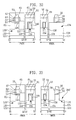
- FIGS. 1A and 1B which may be referred to herein collectively as FIG. 1 , and FIGS. 2 to 4 , are cross-sectional views for describing a semiconductor device in accordance with embodiments of the inventive concepts;
- FIG. 5 is a layout for describing a method of forming a semiconductor device in accordance with an embodiment of the inventive concepts
- FIGS. 6 to 24 are cross-sectional views for describing the method of forming a semiconductor device in accordance with the embodiment of the inventive concepts
- FIG. 25 is a layout for describing a method of forming a semiconductor device in accordance with another embodiment of the inventive concepts.
- FIGS. 26 to 44 are cross-sectional views for describing the method of forming a semiconductor device in accordance with another embodiment of the inventive concepts
- FIG. 45 is a layout for describing a method of forming a semiconductor device in accordance with still another embodiment of the inventive concepts.
- FIGS. 46 and 47 are cross-sectional views for describing the method of forming a semiconductor device in accordance with still another embodiment of the inventive concepts.
- FIGS. 48 and 49 are system block diagrams of electronic devices in accordance with an embodiment of the inventive concepts.
- inventive concepts should not be limited to the embodiments set forth herein and may be construed as various embodiments in different forms. Rather, these embodiments are provided so that disclosure of the inventive concepts is thorough and complete, and fully conveys the inventive concepts to those of ordinary skill in the art.
- inventive concepts are defined by the appended claims.
- spatially relative terms such as “below,” “beneath,” “lower,” “above,” “upper,” and the like, may be used herein to easily describe the correlation between one device or elements and another device or other elements as illustrated in the figures.
- the spatially relative terms should be understood as terms that include different orientations of the device in additional usage or operation of the orientations illustrated in figures. For example, when the device illustrated in the figures is turned over, the device described as disposed “below” or “beneath” another device may be disposed “above” the other device. Accordingly, the exemplary term “below” or “beneath” may include both orientations of below and above.
- the device may be oriented at other orientations, and the spatially relative terms used herein may be interpreted accordingly.
- embodiments are described herein with reference to cross-sectional views and/or plan views that are idealized schematic views of the inventive concepts.
- the thicknesses of layers and parts in the figures may be overstated for the effective description of technical content, except when indicated to the contrary therein.
- shapes of the schematic views may vary according to manufacturing techniques and/or tolerances. Therefore, the embodiments of the inventive concepts are not limited to the particular shapes illustrated herein but are to include deviations in shapes formed in accordance with the manufacturing process.
- an etched region illustrated as a rectangular shape may be a rounded shape or a shape of a certain curvature.
- the regions illustrated in the figures are schematic in nature, and the shapes of the regions illustrated in the figures are intended to illustrate particular shapes of regions of devices and not intended to limit the scope of the inventive concepts, unless indicated to the contrary herein.
- front side and back side are used herein as relative concepts to describe the embodiments of the inventive concepts for easy understanding.
- front side and back side do not necessarily indicate specific directions, locations, or elements but can be used interchangeably.
- a term “front side” may be interpreted as a term “back side,” and a term “back side” may be interpreted as a term “front side.” Accordingly, the term “front side” may be expressed as a term “first side,” and a term “back side” may be expressed as a term “second side.” Conversely, a term “back side” may be expressed as a term “first side,” and a term “front side” may be expressed as a term “second side.” However, the terms “front side” and “back side” are not used in the same sense in one embodiment.
- a term such as “near” used herein indicates that any one of at least two elements having symmetrical concepts is disposed nearer to another specific element than the others thereof.
- the expression such as a first end is close to a first side may be inferred as the first end is closer to the first side than a second end, or the first end is closer to the first side than a second side.
- FIGS. 1A and 1B which may be referred to herein collectively as FIG. 1 , and FIGS. 2 to 4 , are cross-sectional views for describing a semiconductor device in accordance with embodiments of the inventive concepts.
- an N-well 123 , a P-well 124 , a first fin active region 133 , a second fin active region 134 , a first device isolation layer 137 , a second device isolation layer 138 , a semiconductor layer 145 , a first lower gate dielectric layer 71 , a second lower gate dielectric layer 72 , a first upper gate dielectric layer 73 , a second upper gate dielectric layer 74 , a first lower gate electrode 75 , a second lower gate electrode 76 , a first upper gate electrode 77 , a second upper gate electrode 78 , a first gate capping layer 81 , a second gate capping layer 82 , and an upper insulating layer 85 may be formed on a semiconductor substrate 121 having an NMOS region and a PMOS region. Although the PMOS and NMOS regions are illustrated as being spaced apart for convenience, it will be understood that a single, unitary semiconductor device, such as a single integrated circuit chip,
- An upper end of the first fin active region 133 may extend to a level lower than an upper end of the second fin active region 134 .
- the upper end of the first fin active region 133 and the upper end of the second fin active region 134 may extend to have a difference of a first thickness d 1 .
- a lower end of the first fin active region 133 may extend to a level lower than a lower end of the second fin active region 134 .
- the lower end of the first fin active region 133 and the lower end of the second fin active region 134 may extend to have a difference of a second thickness d 2 .
- An upper end of the first device isolation layer 137 may extend to a level lower than the upper end of the first fin active region 133 .
- a side surface and the upper end of the first fin active region 133 may protrude from the upper end of the first device isolation layer 137 .
- An upper end of the second device isolation layer 138 may extend to a level lower than the upper end of the second fin active region 134 .
- a side surface and the upper end of the second fin active region 134 may protrude from the upper end of the second device isolation layer 138 .
- the upper end of the first device isolation layer 137 may extend to a level lower than the upper end of the second device isolation layer 138 .
- the upper end of the first device isolation layer 137 and the upper end of the second device isolation layer 138 may have a difference of a third thickness d 3 .
- a lower end of the first device isolation layer 137 may directly contact the N-well 123 .
- a lower end of the second device isolation layer 138 may directly contact the P-well 124 .
- the lower end of the first device isolation layer 137 may extend to a level lower than the lower end of the second device isolation layer 138 .
- the semiconductor layer 145 may extend on the first fin active region 133 .
- the semiconductor layer 145 may directly contact the side surfaces and an upper surface of the first fin active region 133 .
- An upper end of the semiconductor layer 145 may extend to the same level as the upper end of the second fin active region 134 .
- a lower end of the semiconductor layer 145 may extend directly on the first device isolation layer 137 .
- the semiconductor layer 145 may include a crystal growth material.
- the semiconductor layer 145 may be defined on side surfaces and the upper surface of the first fin active region 133 .
- the semiconductor layer 145 may extend partially on an upper level of the first device isolation layer 137 .
- the semiconductor layer 145 may include N-type impurities.
- the semiconductor layer 145 may include SiGe, Si, P and/or As.
- the semiconductor layer 145 may include SiGe formed by a selective epitaxial growth (SEG) method.
- An amount of Ge contained in the semiconductor layer 145 may be in a range of approximately 25 to approximately 50%.
- An amount of Ge contained in the semiconductor layer 145 may be approximately 30%.
- Upper surfaces of the first upper gate electrode 77 and the second upper gate electrode 78 may extend to the same plane.
- the first fin active region 133 may be in the NMOS region, and the second fin active region 134 may be in the PMOS region.
- the first fin active region 133 may include P-type impurities.
- the semiconductor layer 145 may include P-type impurities.
- the semiconductor layer 145 may include SiC, Si, B and/or BF.
- a semiconductor device include a substrate S having a face F.
- either one of the opposing faces of the semiconductor substrate S may be regarded as the face F.
- a first fin F 1 is on the face F and protrudes away from the face F.
- the first fin F 1 has a first fin bottom F 1 b adjacent the face F, a first fin top F 1 t remote from the face F and the first fin sidewall F 1 s that extends between the first fin top F 1 t and the first fin bottom F 1 b .
- a second fin F 2 is also provided on the face F and protrudes away from the face F.
- the second fin F 2 has a second fin bottom F 2 b adjacent the face F, a second fin top F 2 t remote from the face F and a second fin sidewall F 2 s that extends between the second fin top F 2 t and the second fin bottom F 2 b .
- the first fin top F 1 t and the second fin top F 2 t are different distances away from the face F, as denoted by distances D 4 and D 5 , respectively.
- the first fin bottom F 1 b and the second fin bottom F 2 b are different distances away from the face F, as denoted by distances D 6 and D 7 , respectively.
- first and second well layers 123 and 124 may also include a first well layer 123 between the face F and the first fin bottom F 1 b , and a second well layer 124 between the face F and the second fin bottom F 2 b .
- the first and second well layers 123 and 124 respectively, have different thicknesses T 1 and T 2 , respectively.
- a first height H 1 of the first fin F 1 is the same as a second height H 2 of the second fin F 2 , from the second fin bottom F 2 b to the second fin top F 2 t.
- the semiconductor device further comprises a first device isolation layer 137 on the first sidewall F 1 s .
- the first device isolation layer 137 has a first device isolation layer bottom DI 1 b adjacent the face F and a first device isolation layer top DI 1 t remote from the face F.
- a second device isolation layer 138 is also provided on the second sidewall F 2 s .
- the second device isolation layer 138 has a second device isolation layer bottom DI 2 b adjacent the face F and a second device isolation layer top DI 2 t remote from the face F.
- the first device isolation layer top DI 1 t and the second device isolation layer top DI 2 t are different distances D 8 , D 9 , respectively, away from the face F.
- first device isolation layer bottom DI 1 b and the second device isolation layer bottom DI 2 b are different distances T 1 , T 2 , respectively, away from the face F.
- first fin F 1 and the first well layer 123 may comprise a conductivity type that is different from that of the second fin F 2 and the second well layer 124 .
- a semiconductor layer 145 also may be provided on the first fin top F 1 t and the first fin sidewall F 1 s .
- the semiconductor layer 145 has a thickness such that a top St of the semiconductor layer 145 that is remote from the first fin top F 1 t is the same distance D 5 away from the face F as the second fin top F 2 t.
- an upper end of a first fin active region 133 A may have a shape different from an upper end of a second fin active region 134 A.
- the upper end of the first fin active region 133 A may be roundly formed.
- the upper end of the first fin active region 133 A may have a first radius of curvature R 1 .
- the upper end of the second fin active region 134 A may be roundly formed.
- the upper end of the second fin active region 134 A may have a second radius of curvature R 2 .
- the first radius of curvature R 1 may be smaller than the second radius of curvature R 2 .
- the first and second fin tops F 1 t , F 2 t respectively, have different radii of curvature R 1 , R 2 , respectively.
- an N-well 23 , a P-well 24 , first fin active regions 33 , second fin active regions 34 , a first device isolation layer 37 , a second device isolation layer 38 , and a semiconductor layer 45 may be on a semiconductor substrate 21 having an NMOS region and a PMOS region.
- the first fin active regions 33 may extend to a level lower than the second fin active regions 34 .
- Upper ends of the first fin active regions 33 may extend to a level lower than upper ends of the second fin active regions 34 .
- the upper ends of the first fin active regions 33 and the upper ends of the second fin active regions 34 may have a difference of a first thickness d 1 .
- Lower ends of the first fin active regions 33 may extend to a level lower than lower ends of the second fin active regions 34 .
- the lower ends of the first fin active regions 33 and the lower ends of the second fin active regions 34 may have a difference of a second thickness d 2 .
- Second fin active regions 34 may protrude from an upper end of the second device isolation layer 38 .
- the upper end of the first device isolation layer 37 may extend to a level lower than the upper end of the second device isolation layer 38 .
- the upper ends of the first device isolation layer 37 and the upper ends of the second device isolation layer 38 may have a difference of a third thickness d 3 .
- Lower ends of the first device isolation layer 37 may extend to a level lower than lower ends of the second device isolation layer 38 .
- a semiconductor layer 45 may be on the first fin active regions 33 .
- An upper end of the semiconductor layer 45 may extend to the same level as the upper ends of the second fin active regions 34 .
- the semiconductor layer 45 may include a crystal growth material.
- the semiconductor layer 45 may extend on the side surfaces and upper surfaces of the first fin active regions 33 .
- the semiconductor layer 45 may include N-type impurities.
- the semiconductor layer 45 may include SiGe, Si, P and/or As.
- the semiconductor layer 45 may include SiGe formed by a SEG method.
- upper ends of first fin active regions 33 A may have shapes different from upper ends of second fin active regions 34 A.
- Each of the upper ends of the first fin active regions 33 A may have a first radius of curvature R 1 .
- Each of the upper ends of the second fin active regions 34 A may have a second radius of curvature R 2 .
- the first radius of curvature R 1 may be smaller than the second radius of curvature R 2 .
- FIG. 5 is a layout for describing a method of forming a semiconductor device in accordance with an embodiment of the inventive concepts
- FIGS. 6 to 24 are cross-sectional views taken along lines I-I′ and II-II′ of FIG. 5 for describing the method of forming the semiconductor device in accordance with the embodiment of the inventive concepts.
- an N-well 23 , a P-well 24 , a pad layer 25 , a first mask layer 26 L, a second mask layer 27 L, a third mask layer 28 L, and a fourth mask pattern 29 may be formed on a semiconductor substrate 21 having an NMOS region and a PMOS region.
- the semiconductor substrate 21 may be a bulk wafer or a silicon on insulator (SOI) wafer.
- the semiconductor substrate 21 may be a single-crystalline silicon wafer having P-type impurities.
- the N-well 23 may be formed in the PMOS region.
- the N-well 23 may include N-type impurities.
- the N-type impurities may include P and/or As.
- the P-well 24 may be formed in the NMOS region.
- the P-well 24 may include P-type impurities.
- the P-type impurities may include B, BF and/or 8 F 2 .
- the pad layer 25 may be on, and in some embodiments cover, the N-well 23 and the P-well 24 .
- the pad layer 25 may include silicon oxide.
- the first mask layer 26 L may be on, and in some embodiments cover, the N-well 23 and the P-well 24 .
- the pad layer 25 may be interposed between the first mask layer 26 L and the N-well 23 and between the first mask layer 26 L and the P-well 24 .
- the second mask layer 27 L may be on, and in some embodiments cover, the first mask layer 26 L.
- the first mask layer 26 L and the second mask layer 27 L may include a material having an etch selectivity with respect to the N-well 23 and the P-well 24 .
- the second mask layer 27 L may include a material different from the first mask layer 26 L.
- the first mask layer 26 L may include silicon nitride
- the second mask layer 27 L may include a Middle Temperature Oxide (MTO).
- MTO Middle Temperature Oxide
- the third mask layer 28 L may include a material having an etch selectivity with respect to the first mask layer 26 L and the second mask layer 27 L.
- the third mask layer 28 L may include a material different from the first mask layer 26 L and the second mask layer 27 L.
- the third mask layer 28 L may include polysilicon.
- the fourth mask pattern 29 may include a material having an etch selectivity with respect to the third mask layer 28 L.
- the fourth mask pattern 29 may include a material different from the third mask layer 28 L.
- the fourth mask pattern 29 may include a Spin On Hardmask (SOH) material.
- SOH Spin On Hardmask
- the fourth mask pattern 29 may be formed by performing a thin layer forming process and a photo process.
- a fifth mask layer 31 L may be formed on the third mask layer 28 L and the fourth mask pattern 29 .
- the fifth mask layer 31 L may be on, and in some embodiments cover, the third mask layer 28 L and side surfaces and an upper surface of the fourth mask pattern 29 .
- the fifth mask layer 31 L may include a material having an etch selectivity with respect to the third mask layer 28 L and the fourth mask pattern 29 .
- the fifth mask layer 31 L may include a material different from the third mask layer 28 L and the fourth mask pattern 29 .
- the fifth mask layer 31 L may include an Atomic Layer Deposition (ALD) oxide.
- ALD Atomic Layer Deposition
- a fifth mask pattern 31 may be formed by anisotropically etching the fifth mask layer 31 L.
- the fifth mask pattern 31 may be interpreted as a spacer.
- the fifth mask pattern 31 may remain on side surfaces of the fourth mask pattern 29 . Upper ends of the fourth mask pattern 29 may be exposed.
- the third mask layer 28 L may be exposed by removing the fourth mask pattern 29 .
- the fifth mask pattern 31 may remain on the third mask layer 28 L.
- a third mask pattern 28 may be formed using the fifth mask pattern 31 as an etch mask and partially removing the third mask layer 28 L. A thickness of the fifth mask pattern 31 may be decreased while forming the third mask pattern 28 .
- a second mask pattern 27 may be formed by partially removing the second mask layer 27 L.
- a first mask pattern 26 may be formed by partially removing the first mask layer 26 L.
- the pad layer 25 may remain between the first mask pattern 26 and the N-well 23 and between the first mask pattern 26 and the P-well 24 .
- An anisotropic etching process which uses the fifth mask pattern 31 and the third mask pattern 28 as etch masks, may be applied in the formation of the second mask pattern 27 and the first mask pattern 26 .
- a thickness of the fifth mask pattern 31 may be decreased or completely removed while forming the second mask pattern 27 and the first mask pattern 26 .
- a plurality of trenches 32 T may be formed using the second mask pattern 27 and the first mask pattern 26 as etch masks.
- First fin active regions 33 in the N-well 23 and second fin active regions 34 in the P-well 24 may be defined by the trenches 32 T.
- An anisotropic etching process may be applied in the formation of the trenches 32 T.
- the third mask pattern 28 may be completely removed while forming the trenches 32 T.
- the first fin active regions 33 may include N-type impurities.
- the first fin active regions 33 may include single-crystalline silicon having N-type impurities.
- the first fin active regions 33 may extend in parallel.
- Each of the first fin active regions 33 may have a height greater than a width thereof.
- the second fin active regions 34 may include P-type impurities.
- the second fin active regions 34 may include single-crystalline silicon having P-type impurities.
- the second fin active regions 34 may be in parallel. Each of the second fin active regions 34 may have a height greater than a width thereof.
- the first fin active regions 33 and the second fin active regions 34 may be exposed by removing the second mask pattern 27 , the first mask pattern 26 , and the pad layer 25 .
- a sixth mask pattern 36 on, and in some embodiments covering, the NMOS region and exposing the PMOS region may be formed.
- the second fin active regions 34 may be at least partially covered by the sixth mask pattern 36 , and the first fin active regions 33 may be exposed.
- the sixth mask pattern 36 may be formed using a photolithography process.
- the first fin active regions 33 may be formed at a level lower than the second fin active regions 34 using an etch-back process.
- the etch-back process may include an anisotropic etching process.
- Upper ends of the first fin active regions 33 may be recessed downward.
- the upper ends of the first fin active regions 33 may be formed at a level lower than upper ends of the second fin active regions 34 .
- the upper ends of the first fin active regions 33 and the upper ends of the second fin active regions 34 may be formed to have a difference of a first thickness d 1 .
- the N-well 23 may also be partially recessed.
- Lower ends of the first fin active regions 33 may be formed at a level lower than lower ends of the second fin active regions 34 .
- the lower ends of the first fin active regions 33 and the lower ends of the second fin active regions 34 may be formed to have a difference of a second thickness d 2 .
- upper ends of the first fin active regions 33 and upper ends of the second fin active regions 34 may be roundly formed.
- the upper ends of the first fin active regions 33 may have shapes different from the upper ends of the second fin active regions 34 .
- the first fin active regions 33 and the second fin active regions 34 may be exposed by removing the sixth mask pattern 36 .
- a first device isolation layer 37 and a second device isolation layer 38 may be formed between the first fin active regions 33 and between the second fin active regions 34 , respectively.
- An upper end of the first device isolation layer 37 may be formed at a level lower than upper ends of the first fin active regions 33 .
- Side surfaces and the upper ends of the first fin active regions 33 may protrude from the upper end of the first device isolation layer 37 .
- An upper end of the second device isolation layer 38 may be formed at a level lower than upper ends of the second fin active regions 34 .
- Side surfaces and the upper ends of the second fin active regions 34 may protrude from the upper end of the second device isolation layer 38 .
- the first device isolation layer 37 and the second device isolation layer 38 may include silicon oxide, silicon nitride and/or silicon oxy-nitride.
- the first device isolation layer 37 and the second device isolation layer 38 may be formed using a Flowable Chemical Vapor Deposition (FCVD) technique, a TOnen SilaZene (TOSZ) technique, or a combination thereof.
- FCVD Flowable Chemical Vapor Deposition
- TOSZ TOnen SilaZene
- the upper end of the first device isolation layer 37 may be formed at a level lower than the upper end of the second device isolation layer 38 .
- the upper end of the first device isolation layer 37 and the upper end of the second device isolation layer 38 may be formed to have a difference of a third thickness d 3 .
- a lower end of the first device isolation layer 37 may directly contact the N-well 23 .
- a lower end of the second device isolation layer 38 may directly contact the P-well 24 .
- the lower end of the first device isolation layer 37 may
- the upper end of the first device isolation layer 37 and the upper end of the second device isolation layer 38 may be formed at the same level.
- a seventh mask layer 39 may be formed.
- the seventh mask layer 39 may be on, and in some embodiments cover, the first device isolation layer 37 , the second device isolation layer 38 , the first fin active regions 33 , and the second fin active regions 34 .
- the seventh mask layer 39 may include a material having an etch selectivity with respect to the first device isolation layer 37 and the second device isolation layer 38 .
- the seventh mask layer 39 may include silicon nitride.
- an eighth mask pattern 42 on, and in some embodiments covering, the NMOS region and exposing the PMOS region may be formed.
- the eighth mask pattern 42 may be formed using a photolithography process.
- the seventh mask layer 39 on the second fin active regions 34 may be at least partially covered by the eighth mask pattern 42 .
- the seventh mask layer 39 on the first fin active regions 33 may be exposed.
- the first fin active regions 33 may be exposed by partially removing the seventh mask layer 39 .
- the eighth mask pattern 42 may be removed.
- the seventh mask layer 39 may remain in the NMOS region.
- the seventh mask layer 39 may at least partially cover the second fin active regions 34 .
- the first fin active regions 33 may be exposed in the PMOS region.
- a semiconductor layer 45 may be formed on the first fin active regions 33 .
- the semiconductor layer 45 may directly contact side surfaces and upper surfaces of the first fin active regions 33 .
- An upper end of the semiconductor layer 45 may be formed at the same level as upper ends of the second fin active regions 34 .
- a lower end of the semiconductor layer 45 may be directly formed on the first device isolation layer 37 .
- the semiconductor layer 45 may include a crystal growth material.
- the semiconductor layer 45 may be defined by side surfaces and upper surfaces of the first fin active regions 33 .
- the semiconductor layer 45 may be restrictively formed on the upper end of the first device isolation layer 37 .
- the semiconductor layer 45 may include N-type impurities.
- the semiconductor layer 45 may include SiGe, Si, P and/or As.
- the semiconductor layer 45 may include SiGe formed by a SEG method.
- An amount of Ge contained in the semiconductor layer 45 may be in a range of approximately 25 to 50%.
- An amount of Ge contained in the semiconductor layer 45 may be approximately 30%.
- the first fin active regions 33 may be formed in the NMOS region, and the second fin active regions 34 may be formed in the PMOS region.
- the first fin active regions 33 may include P-type impurities.
- the semiconductor layer 45 may include P-type impurities.
- the semiconductor layer 45 may include SiC, Si, B and/or BF.
- the second fin active regions 34 may be exposed by removing the seventh mask layer 39 .
- upper ends of first fin active regions 33 A may have shapes different from upper ends of second fin active regions 34 A.
- Each of the upper ends of the first fin active regions 33 A may be roundly formed.
- Each of the upper ends of the first fin active regions 33 A may have a first radius of curvature R 1 .
- Each of the upper ends of the second fin active regions 34 A may be roundly formed.
- Each of the upper ends of the second fin active regions 34 A may have a second radius of curvature R 2 .
- the first radius of curvature R 1 may be smaller than the second radius of curvature R 2 .
- FIG. 25 is a layout for describing a method of forming a semiconductor device in accordance with another embodiment of the inventive concepts
- FIGS. 26 to 44 are cross-sectional views taken along lines III-III′, IV-IV′, V-V′, and VI-VI′ of FIG. 25 for describing the method of forming a semiconductor device in accordance with another embodiment of the inventive concepts.
- an N-well 123 , a P-well 124 , a first fin active region 133 , a second fin active region 134 , a first device isolation layer 137 , a second device isolation layer 138 , and a semiconductor layer 145 may be formed on a semiconductor substrate 121 having an NMOS region and a PMOS region.
- the semiconductor substrate 121 , the N-well 123 , the P-well 124 , the first fin active region 133 , the second fin active region 134 , the first device isolation layer 137 , the second device isolation layer 138 , and the semiconductor layer 145 may be formed by a similar method described with reference to FIGS. 5 to 24 .
- a preliminary buffer layer 51 L, a preliminary gate layer 53 L, and a preliminary capping layer 55 L may be sequentially formed on the semiconductor substrate 121 .
- the preliminary buffer layer 51 L may include silicon oxide.
- the preliminary gate layer 53 L may include polysilicon.
- the preliminary capping layer 55 L may include silicon oxide, silicon nitride and/or silicon oxy-nitride.
- a first preliminary buffer pattern 51 , a first preliminary gate pattern 53 , and a first preliminary capping pattern 55 may be formed by patterning the preliminary buffer layer 51 L, the preliminary gate layer 53 L, and the preliminary capping layer 55 L in the PMOS region.
- the first preliminary gate pattern 53 may be on, and in some embodiments cover, an upper portion and side surfaces of the semiconductor layer 145 and extend to the first device isolation layer 137 .
- the first preliminary buffer pattern 51 may remain between the first preliminary gate pattern 53 and the semiconductor layer 145 .
- the preliminary buffer layer 51 L, the preliminary gate layer 53 L, and the preliminary capping layer 55 L may remain in the NMOS region.
- First inner spacers 57 may be formed on side surfaces of the first preliminary gate pattern 53 .
- the formation of the first inner spacers 57 may include a thin layer forming process and an anisotropic etching process.
- the first inner spacers 57 may include an insulating layer formed of silicon oxide, silicon nitride and/or silicon oxy-nitride.
- the first inner spacers 57 may include silicon nitride.
- the semiconductor layer 145 may be exposed on outer surfaces of the first preliminary gate pattern 53 and the first inner spacers 57 .
- a first recessed area 57 T may be formed by partially removing the semiconductor layer 145 and the first fin active region 133 .
- An anisotropic etching process, an isotropic etching process and/or a directional etching process may be applied in the formation of the first recessed area 57 T.
- the first recessed area 57 T may be aligned on outer surfaces of the first inner spacers 57 .
- the first recessed area 57 T may expand to a lower portion of the first inner spacer 57 .
- a bottom of the first recessed area 57 T may be formed at a level lower than a lower end of the first preliminary gate pattern 53 .
- the semiconductor layer 145 and the first fin active region 133 may be exposed on sidewalls and a bottom of the first recessed area 57 T.
- a bottom of the first inner spacer 57 may be exposed in the first recessed area 57 T.
- a first source/drain 61 may be formed in the first recessed area 57 T.
- the first source/drain 61 may directly contact the semiconductor layer 145 and the first fin active region 133 .
- the first source/drain 61 may include a crystal growth material.
- the first source/drain 61 may include SiGe and/or Si.
- the first source/drain 61 may fill the first recessed area 57 T and protrude at a level higher than an upper end of the semiconductor layer 145 .
- the first source/drain 61 may be interpreted as an elevated source/drain.
- the first source/drain 61 may be interpreted as a stressor.
- the first source/drain 61 may include P-type impurities.
- the first source/drain 61 may include B and/or BF.
- the first source/drain 61 may include a SiGe layer formed by using a SEG method. An upper end of the first source/drain 61 may protrude at a level higher than a lower end of the first inner spacer 57 .
- An amount of Ge contained in the first source/drain 61 may be in a range of approximately 0 to 50%.
- An amount of Ge contained in the first source/drain 61 may be different from an amount of Ge in the semiconductor layer 145 .
- An amount of Ge contained in the first source/drain 61 may be less than an amount of Ge in the semiconductor layer 145 .
- an amount of Ge contained in the semiconductor layer 145 may be approximately 30%, and an amount of Ge contained in the first source/drain 61 may be in a range of approximately 10 to 30%.
- a first source/drain 61 may include a first lower semiconductor layer, a first middle semiconductor layer, and a first upper semiconductor layer.
- the first lower semiconductor layer may include an undoped single-crystalline SiGe formed by a SEG method.
- An amount of Ge contained in the first lower semiconductor layer may be in a range of approximately 10 to 25%.
- the first lower semiconductor layer may conformally extend on, and in some embodiments cover, an inner wall of the first recessed area 57 T.
- the first middle semiconductor layer may be formed on the first lower semiconductor layer.
- the first middle semiconductor layer may completely fill the first recessed area 57 T.
- An upper end of the first middle semiconductor layer may protrude at a level higher than an upper end of the semiconductor layer 145 .
- the first middle semiconductor layer may include boron (B) doped single-crystalline Site formed by a SEG method. An amount of Ge contained in the first middle semiconductor layer may be in a range of approximately 25 to 50%.
- the first middle semiconductor layer may contain boron (B) in a range of approximately 1E20 to 3E20 atom/cm3.
- the first upper semiconductor layer may be formed on the first middle semiconductor layer.
- the first upper semiconductor layer may include boron (B) doped single-crystalline Si formed by a SEG method.
- the first upper semiconductor layer may contain boron (B) in a range of approximately 1E20 to 3E20 atom/cm 3 .
- first outer spacers 63 may be formed on side surfaces of the first inner spacers 57 . Bottoms of the first outer spacers 63 may contact upper surfaces of the first source/drain 61 .
- the formation of the first outer spacers 63 may include a thin layer forming process and an anisotropic etching process.
- the first outer spacers 63 may include an insulating layer formed of silicon oxide, silicon nitride and/or silicon oxy-nitride.
- the first outer spacers 63 may include silicon nitride.
- a first lower insulating layer 65 may be formed on the first source/drain 61 .
- the first lower insulating layer 65 may include an insulating layer formed of silicon oxide, silicon nitride and/or silicon oxy-nitride.
- the first lower insulating layer 65 may include silicon oxide.
- a second preliminary buffer pattern 52 , a second preliminary gate pattern 54 , and a second preliminary capping pattern 56 may be formed by patterning the preliminary buffer layer 51 L, the preliminary gate layer 53 L, and the preliminary capping layer 55 L in the NMOS region.
- the second preliminary gate pattern 54 may be on, and in some embodiments cover, an upper portion and side surfaces of the second fin active region 134 and extend to the second device isolation layer 138 .
- the second preliminary buffer pattern 52 may remain between the second preliminary gate pattern 54 and the second fin active region 134 .
- Second inner spacers 58 may be formed on side surfaces of the second preliminary gate pattern 54 .
- the formation of the second inner spacers 58 may include a thin layer forming process and an anisotropic etching process.
- the second inner spacers 58 may include an insulating layer formed of silicon oxide, silicon nitride and/or silicon oxy-nitride.
- the second inner spacers 58 may include silicon nitride.
- the second fin active region 134 may be exposed on outer surfaces of the second preliminary gate pattern 54 and the second inner spacers 58 .
- second recessed areas 58 T may be formed by partially removing the second fin active region 134 .
- An anisotropic etching process, an isotropic etching process and/or a directional etching process may be applied in the formation of the second recessed areas 58 T.
- the second recessed areas 58 T may be aligned on outer surfaces of the second inner spacers 58 .
- the second recessed areas 58 T may be expanded to a lower portion of the second inner spacers 58 .
- a bottom of the second recessed area 58 T may be formed at a level lower than a lower end of the second preliminary gate pattern 54 .
- the second fin active region 134 may be exposed on sidewalls and bottoms of the second recessed areas 58 T.
- a bottom of the second inner spacer 58 may be exposed in the second recessed area 58 T.
- a second source/drain 62 may be formed in the second recessed area 58 T.
- the second source/drain 62 may include a crystal growth material.
- the second source/drain 62 may include SiC, Si, or a combination thereof.
- the second source/drain 62 may fill the second recessed areas 58 T and protrude at a level higher than an upper end of the second fin active region 134 .
- the second source/drain 62 may be referred to as an elevated source/drain.
- the second source/drain 62 may be interpreted as a stressor.
- the second source/drain 62 may include N-type impurities.
- the second source/drain 62 may include P and/or As.
- the second source/drain 62 may include a SiC layer formed by using a SEG method.
- An upper end of the second source/drain 62 may protrude at a level higher than a lower end of the second inner spacer 58 .
- the second source/drain 62 may include a second lower semiconductor pattern and a second upper semiconductor layer.
- the second lower semiconductor pattern may be formed by implanting N-type impurities in the second fin active region 134 .
- the second upper semiconductor layer may be formed on the second lower semiconductor pattern using a SEG method.
- the second upper semiconductor layer may include a Si layer.
- the second upper semiconductor layer may include N-type impurities.
- second outer spacers 64 may be formed on side surfaces of the second inner spacers 58 . Bottoms of the second outer spacers 64 may contact an upper surface of the second source/drain 62 .
- the formation of the second outer spacers 64 may include a thin layer forming process and an anisotropic etching process.
- the second outer spacers 64 may include an insulating layer formed of silicon oxide, silicon nitride and/or silicon oxy-nitride.
- the second outer spacers 64 may include silicon nitride.
- the upper surface of the second source/drain 62 may be exposed on outer surfaces of the second outer spacers 64 .
- a second lower insulating layer 66 may be formed on the second source/drain 62 .
- the formation of the second lower insulating layer 66 may include a thin layer forming process and a planarization process.
- the planarization process may include a Chemical Mechanical Polishing (CMP) process and/or an etch-back process.
- the second lower insulating layer 66 may include an insulating layer formed of silicon oxide, silicon nitride and/or silicon oxy-nitride.
- the second lower insulating layer 66 may include silicon oxide.
- the first preliminary gate pattern 53 and the second preliminary gate pattern 54 may be exposed using a CMP process.
- the first preliminary capping pattern 55 and the second preliminary capping pattern 56 may be removed.
- first gate trenches 53 T and second gate trenches 54 T may be formed by removing the first preliminary gate pattern 53 , the second preliminary gate pattern 54 , the first preliminary buffer pattern 51 , and the second preliminary buffer pattern 52 .
- An upper surface and side surfaces of the semiconductor layer 145 may be exposed in the first gate trench 53 T.
- An upper surface and side surfaces of the second fin active region 134 may be exposed in the second gate trench 54 T.
- a first lower gate dielectric layer 71 and a second lower gate dielectric layer 72 may be formed.
- the first lower gate dielectric layer 71 may be formed on an upper surface and side surfaces of the semiconductor layer 145 .
- the first lower gate dielectric layer 71 may be defined on the upper surface and the side surfaces of the semiconductor layer 145 .
- the second lower gate dielectric layer 72 may be formed on an upper surface and side surfaces of the second fin active region 134 .
- the second lower gate dielectric layer 72 may be defined on the upper surface and the side surfaces of the second fin active region 134 .
- the first lower gate dielectric layer 71 and the second lower gate dielectric layer 72 may be referred to as an interfacial oxide layer or a chemical oxide layer.
- the first lower gate dielectric layer 71 and the second lower gate dielectric layer 72 may be formed by performing a cleaning process.
- the first lower gate dielectric layer 71 and the second lower gate dielectric layer 72 may include silicon oxide formed by a chemical reaction of Si and H 2 O 2 .
- a first upper gate dielectric layer 73 , a first lower gate electrode layer 75 L, and a first upper gate electrode layer 77 L may be formed on the first lower gate dielectric layer 71 .
- a second upper gate dielectric layer 74 , a second lower gate electrode layer 76 L, and a second upper gate electrode layer 78 L may be formed on the second lower gate dielectric layer 72 .
- the first upper gate dielectric layer 73 and the second upper gate dielectric layer 74 may include silicon oxide, silicon nitride, silicon oxy-nitride and/or a high-K dielectric layer.
- the first upper gate dielectric layer 73 and the second upper gate dielectric layer 74 may include HfO and/or HfSiO.
- Each of the first lower gate electrode layer 75 L and the second lower gate electrode layer 76 L may include a conductive layer having a work-function.
- Each of the first lower gate electrode layer 75 L and the second lower gate electrode layer 76 L may include TiN, TaN, TiAl and/or TiAlC.
- the first lower gate electrode layer 75 L may include a material different from the second lower gate electrode layer 76 L.
- the first upper gate electrode layer 77 L and the second upper gate electrode layer 78 L may include a metal layer, a metal silicide layer, a conductive carbon layer and/or a polysilicon layer.
- first lower gate electrodes 75 , first upper gate electrodes 77 , second lower gate electrodes 76 , and second upper gate electrodes 78 may be formed using a planarization process.
- the first lower gate electrodes 75 may surround side surfaces and a bottoms of the first upper gate electrodes 77 .
- the first upper gate dielectric layer 73 may surround side surfaces and bottoms of the first lower gate electrodes 75 .
- the first lower gate dielectric layer 71 may be interposed between the semiconductor layer 145 and the first upper gate dielectric layer 73 .
- the second lower gate electrodes 76 may surround side surfaces and bottoms of the second upper gate electrodes 78 .
- the second upper gate dielectric layer 74 may surround side surface and bottoms of the second lower gate electrode 76 .
- the second lower gate dielectric layer 72 may be interposed between the second fin active region 134 and the second upper gate dielectric layer 74 .
- an upper end of the first fin active region 133 may be formed at a level lower than an upper end of the second fin active region 134 .
- An upper end of the semiconductor layer 145 may be formed at substantially the same level as the upper end of the second fin active region 134 .
- Upper surfaces of the first lower insulating layer 65 , the second lower insulating layer 66 , the first upper gate electrode 77 , and the second upper gate electrode 78 may be exposed in substantially the same plane.
- first gate recessed areas 77 R and second gate recessed areas 78 R may be formed by performing an etch-back process to the first lower gate electrode 75 , the first upper gate electrode 77 , the second lower gate electrode 76 , and the second upper gate electrode 78 .
- a first gate capping layer 81 and a second gate capping layer 82 may be formed in the first gate recessed area 77 R and the second gate recessed area 78 R.
- the first gate capping layer 81 and the second gate capping layer 82 may include an insulating layer formed of silicon oxide, silicon nitride and/or silicon oxy-nitride.
- the first gate capping layer 81 and the second gate capping layer 82 may include silicon nitride.
- an upper insulating layer 85 on, and in some embodiments covering, the PMOS region and the NMOS region may be formed.
- the upper insulating layer 85 may include an insulating layer formed of silicon oxide, silicon nitride and/or silicon oxy-nitride.
- the upper insulating layer 85 may include silicon oxide.
- an upper end of a first fin active region 133 A may have a shape different from an upper end of a second fin active region 134 A.
- the upper end of the first fin active region 133 A may be roundly formed.
- the upper end of the first fin active region 133 A may have a first radius of curvature R 1 .
- the upper end of the second fin active region 134 A may be roundly formed.
- the upper end of the second fin active region 134 A may have a second radius of curvature R 2 .
- the first radius of curvature R 1 may be smaller than the second radius of curvature R 2 .
- FIG. 45 is a layout for describing a method of forming a semiconductor device in accordance with still another embodiment of the inventive concepts
- FIGS. 46 and 47 are cross-sectional views taken along lines VII-VII′, VIII-VIII′, IX-IX′ and X-X′ of FIG. 45 for describing the method of forming a semiconductor device in accordance with still another embodiment of the inventive concepts.
- the plurality of first fin active regions 233 may extend in parallel.
- the plurality of second fin active regions 234 may extend in parallel.
- the plurality of first upper gate electrodes 277 may extend in parallel.
- the plurality of second upper gate electrodes 278 may extend in parallel.
- Each of the plurality of first upper gate electrodes 277 may cross the plurality of first fin active regions 233 .
- Each of the plurality of second upper gate electrodes 278 may cross the plurality of second fin active regions 234 .
- upper ends of first fin active regions 233 A may have shapes different from upper ends of second fin active regions 234 A.
- An upper end of each of the first fin active regions 233 A may have a first radius of curvature R 1 .
- An upper end of each of the second fin active regions 234 A may have a second radius of curvature R 2 .
- the first radius of curvature R 1 may be smaller than the second radius of curvature R 2 .
- FIGS. 48 and 49 are system block diagrams of electronic devices in accordance with an embodiment of the inventive concepts.
- the electronic system 2100 may include a body 2110 , a microprocessor 2120 , a power 2130 , a function unit 2140 , and a display controller 2150 .
- the body 2110 may include a motherboard formed with a printed circuit board (PCB).
- the body 2110 may include the microprocessor 2120 , the power 2130 , the function unit 2140 , and the display controller 2150 .
- a display 2160 may be disposed inside the body 2110 or outside the body 2110 .
- the display 2160 may be disposed on a surface of the body 2110 and display an image processed by the display controller 2150 .
- the power 2130 may receive a predetermined voltage from an external battery, divide the predetermined voltage into required voltage levels, and serve to supply the voltages to the microprocessor 2120 , the function unit 2140 , and the display controller 2150 .
- the microprocessor 2120 may receive a voltage from the power 2130 and control the function unit 2140 and the display 2160 .
- the function unit 2140 may perform various functions of the electronic system 2100 .
- the function unit 2140 may include dialing or various components to perform mobile functions such as an image output to the display 2160 or an audio output to a speaker from communication with an external apparatus 2170 , and the function unit 2140 may also serve as a camera image processor when a camera is mounted on the smart phone.
- the function unit 2140 may serve as a memory card controller.
- the function unit 2140 may exchange a signal with the external apparatus 2170 via either a wired or wireless communication unit 2180 .
- the function unit 2140 may serve as an interface controller.
- the function unit 2140 may include a mass capacity storage unit.
- a semiconductor device similar to those described with reference to FIGS. 1 to 47 may apply to the function unit 2140 , the microprocessor 2120 and/or any of the other blocks of FIG. 48 .
- the microprocessor 2120 may include the first fin active region 133 and the semiconductor layer 145 .
- an electronic system 2400 may include at least one of the semiconductor devices according to the embodiments of the inventive concepts.
- the electronic system 2400 may provide a component of a mobile device or a computer.
- the electronic system 2400 may include a memory system 2412 , a microprocessor 2414 , a RAM 2416 , a bus 2420 , and a user interface 2418 .
- the microprocessor 2414 , the memory system 2412 , and the user interface 2418 may be mutually connected via the bus 2420 .
- the user interface 2418 may be used for data input to the electronic system 2400 or data output from the electronic system 2400 .
- the microprocessor 2414 may program and control the electronic system 2400 .
- the RAM 2416 may be used as an operational memory of the microprocessor 2414 .
- the microprocessor 2414 , the RAM 2416 and/or other components may be assembled in a single package.
- the memory system 2412 may store operational codes of the microprocessor 2414 , data processed by the microprocessor 2414 , or externally input data.
- the memory system 2412 may include a controller and a memory.
- a semiconductor device similar to those described with reference to FIGS. 1 to 47 may apply to the microprocessor 2414 , the RAM 2416 , the memory system 2412 and/or the user interface 2418 .
- a first active region defined in a PMOS region and a second active region defined in an NMOS region are formed.
- a semiconductor layer is formed on the first active region.
- a first gate electrode on the semiconductor layer and a second gate electrode on the second active region are formed.
- An upper end of the first active region is formed at a level lower than an upper end of the second active region.
- An upper end of the semiconductor layer may be formed at substantially the same horizontal level as the upper end of the second active region.
- a process is simplified and heights of the first gate electrode and the second gate electrode may be formed at certain levels.
Abstract
A semiconductor device has active regions with different conductivity types. A substrate has a PMOS region and an NMOS region. A first active region is in the PMOS region. A second active region is in the NMOS region. A semiconductor layer is on the first active region. A first gate electrode crosses the first active region and extends on the semiconductor layer. A second gate electrode is on the second active region. An upper end of the first active region extends to a level lower than an upper end of the second active region. A lower end of the first active region extends to a level lower than a lower end of the second active region.
Description
This application claims priority under 35 U.S.C. §119 to Korean Patent Application No. 10-2014-0136844 filed on Oct. 10, 2014, the disclosure of which is hereby incorporated by reference in its entirety.
Embodiments of the inventive concepts relate to semiconductor devices having active regions of different conductivity types.
Various methods of forming upper ends of gate electrodes at certain levels while simplifying a process in a semiconductor device having an NMOS region and a PMOS region have been studied. A P-type channel region formed in the NMOS region and an N-type channel region formed in the PMOS region may have different heights. The P-type channel region and the N-type channel region having the different heights may be an obstacle to formation of gate electrodes.
For example, an N-type fin may be formed on an N-well, and a P-type fin may be formed on a P-well. A channel SiGe layer may be formed on the N-type fin using a Selective Epitaxial Growth (SEG) technique. A first preliminary gate may be formed on the channel SiGe layer, and a second preliminary gate may be formed on the P-type fin. A first source/drain may be formed on both sides of the first preliminary gate. A second source/drain may be formed on both sides of the second preliminary gate. An interlayer insulating layer may be formed on the first source/drain and the second source/drain. A first trench and a second trench may be formed by removing the first preliminary gate and the second preliminary gate. A first gate and a second gate may be formed in the first trench and the second trench. The first gate and the second gate may be referred to as a replacement gate.
A process of forming the first gate and the second gate may include a Chemical Mechanical Polishing (CMP) process. The channel SiGe layer may protrude at a level higher than the P-type fin. Various problems may arise from a height difference between the first gate and the second gate in the CMP process.
Various embodiments of the inventive concepts are not limited to the presently-mentioned embodiments; other embodiments which are not mentioned may be clearly understood by those of ordinary skill in the art based on the following descriptions.
In accordance with an aspect of the inventive concepts, a semiconductor device includes a substrate having a PMOS region and an NMOS region. A first active region is in the PMOS region. A second active region is in the NMOS region. A semiconductor layer is on the first active region. A first gate electrode is configured to cross the first active region and extend on the semiconductor layer. A second gate electrode is on the second active region. An upper end of the first active region extends to a level lower than an upper end of the second active region. A lower end of the first active region extends to a level lower than a lower end of the second active region.
In an embodiment, an upper end of the semiconductor layer may extend to a same horizontal level as the upper end of the second active region.
In another embodiment, upper ends of the first gate electrode and the second gate electrode may extend to the same horizontal level.
In still another embodiment, an upper end of the first active region may have a shape different from an upper end of the second active region.
In yet another embodiment, an upper end of the first active region may have a first radius of curvature. An upper end of the second active region may have a second radius of curvature. The first radius of curvature may be smaller than the second radius of curvature.
In yet another embodiment, the semiconductor layer may include a crystal growth material.
In yet another embodiment, the semiconductor layer may include SiGe formed by a Selective Epitaxial Growth (SEG) method.
In yet another embodiment, the semiconductor layer may be on side surfaces and an upper surface of the first fin active region.
In yet another embodiment, the first active region may have a height greater than a width thereof, and a lower end of the first gate electrode may extend to a level lower than an upper end of the first active region. The second active region may have a height greater than a width thereof, and a lower end of the second gate electrode may extend to a level lower than an upper end of the second active region.
In yet another embodiment, a gate dielectric layer is on, and in some embodiments surrounds, a bottom and a side surface of the first gate electrode. An upper end of the gate dielectric layer may extend to a level higher than a center of the first gate electrode.
In yet another embodiment, a first device isolation layer is on a side surface of the first active region. A second device isolation layer is on a side surface of the second active region. A lower end of the first device isolation layer extends to a level lower than a lower end of the second device isolation layer.
In yet another embodiment, an upper end of the first device isolation layer may extend to a level lower than an upper end of the second device isolation layer.
In yet another embodiment, a lower end of the semiconductor layer may extend to a level higher than the first device isolation layer.
In accordance with another aspect of the inventive concepts, another semiconductor device includes a substrate having a first region and a second region which has a conductivity type different from the first region. A first active region is in the first region. A second active region is in the second region. A semiconductor layer is on the first active region and has impurities of the same conductivity type as the first active region. An upper end of the first active region extends to a level lower than an upper end of the second active region. A lower end of the first active region extends to a level lower than a lower end of the second active region. An upper end of the semiconductor layer extends to the same horizontal level as the upper end of the second active region.
In an embodiment, the semiconductor layer may extend on a surface of the first active region.
In another embodiment, the semiconductor layer may include a crystal growth material.
In accordance with still another aspect of the inventive concepts, another semiconductor device includes a substrate having a first region and a second region which has a conductivity type different from the first region. A plurality of first active regions are in the first region and configured to be parallel to one another. A plurality of second active regions are in the second region and configured to be parallel to one another. A semiconductor layer is on the first active regions. A first gate electrode crosses the first active regions and is on the semiconductor layer. A second gate electrode is on the second active regions. Upper ends of the first active regions extend to levels lower than upper ends of the second active regions. Lower ends of the first active regions extend to levels lower than lower ends of the second active regions.
In an embodiment, the semiconductor layer may include impurities having a conductivity type the same as the first active regions. An upper end of the semiconductor layer may extend to the same horizontal level as the upper ends of the second active regions.
In another embodiment, a first device isolation layer is between the first active regions. A second device isolation layer is between the second active regions. An upper end of the first device isolation layer may extend to a level lower than an upper end of the second device isolation layer.
In still another embodiment, a source/drain is adjacent to an outer surface of the first gate electrode and is in contact with the semiconductor layer. The source/drain may include impurities having a conductivity type different from the semiconductor layer.
In accordance with yet another aspect of the inventive concepts, another semiconductor device includes a substrate having a face; a first fin on the face that protrudes away from the face, the first fin having a first fin bottom adjacent the face; a first fin top remote from the face and a first fin sidewall that extends between the first fin top and the first fin bottom; and a second fin on the face that protrudes away from the face, the second fin having a second fin bottom adjacent the face, a second fin top remote from the face and a second fin sidewall that extends between the second fin top and the second fin bottom. The first fin top and the second fin top are different distances away from the face. Also, the first fin bottom and the second fin bottom are different distances away from the face.
In an embodiment, the device further comprises a first well layer between the face and the first fin bottom; and a second well layer between the face and the second fin bottom. The first and second well layers have different thicknesses. In some embodiments, a first height of the first fin, from the first fin bottom to the first fin top, is same as a second height of the second fin, from the second fin bottom to the second fin top. Moreover, in some embodiments, the first and second fin tops have different radii of curvature.
In another embodiment, the semiconductor device further comprises a first device isolation layer on the first sidewall, the first device isolation layer having a first device isolation layer bottom adjacent the face and a first device isolation layer top remote from the face; and a second device isolation layer on the second sidewall, the second device isolation layer having a second device isolation layer bottom adjacent the face and a second device isolation layer top remote from the face. The first device isolation layer top and the second device isolation layer top are different distances away from the face. Also, the first device isolation layer bottom and the second device isolation layer bottom are different distances away from the face.
In still another embodiment, the semiconductor device further comprises a first well layer between the face and the first fin bottom and between the face and the first device isolation layer bottom; and a second well layer between the face and the second fin bottom and between the face and the second device isolation layer bottom. The first and second well layers have different thicknesses.
In yet another embodiment, the first fin and the first well layer comprise a conductivity type that is different from that of the second fin and second well layer.
Finally, in still other embodiments, the semiconductor device further comprises a semiconductor layer on the first fin top and the first fin sidewall and having a thickness such that a top of the semiconductor layer that is remote from the first fin top is same distance away from the face as the second fin top.
Detailed items of the other embodiments of the inventive concepts are included in the detailed descriptions and the accompanying drawings.
The foregoing and other features and advantages of the inventive concepts will be apparent from the more particular description of various embodiments of the inventive concepts, as illustrated in the accompanying drawings in which like reference characters refer to the same parts throughout the different views. The drawings are not to scale except when indicated to the contrary herein, emphasis instead being placed upon illustrating the principles of the inventive concepts. In the drawings:
Advantages and features of the inventive concepts and methods of achieving them will be made apparent with reference to the accompanying figures and the embodiments to be described below in detail. However, the inventive concepts should not be limited to the embodiments set forth herein and may be construed as various embodiments in different forms. Rather, these embodiments are provided so that disclosure of the inventive concepts is thorough and complete, and fully conveys the inventive concepts to those of ordinary skill in the art. The inventive concepts are defined by the appended claims.
The terminology used herein is only intended to describe embodiments of the inventive concepts and not intended to limit the scope of the inventive concepts. As used herein, the singular forms “a,” “an,” and “the” are intended to include the plural forms as well, unless specifically indicated otherwise. The terms “comprises”, “comprising”, “has”, “having”, “includes” and/or “including”, and variants thereof, that are used herein specify the presence of mentioned elements, steps, operations, and/or devices, but do not preclude the presence or addition of one or more of Other elements, steps, operations, and/or devices.
When one element (elements) is (are) “connected” or “coupled” to other element(s), this may indicate that the one element (elements) is directly connected or coupled to the other elements(s), or intervening elements may be present. On the other hand, when one element referred to as “directly connected (directly connected to)” or “directly coupled (directly coupled to)” other element(s), there are no intervening element(s). Throughout the entire specification, the same reference numerals refer to the same components. The phrase “and/or” includes each and all combinations of one or more of the items mentioned.
Spatially relative terms, such as “below,” “beneath,” “lower,” “above,” “upper,” and the like, may be used herein to easily describe the correlation between one device or elements and another device or other elements as illustrated in the figures. The spatially relative terms should be understood as terms that include different orientations of the device in additional usage or operation of the orientations illustrated in figures. For example, when the device illustrated in the figures is turned over, the device described as disposed “below” or “beneath” another device may be disposed “above” the other device. Accordingly, the exemplary term “below” or “beneath” may include both orientations of below and above. The device may be oriented at other orientations, and the spatially relative terms used herein may be interpreted accordingly.
Further, embodiments are described herein with reference to cross-sectional views and/or plan views that are idealized schematic views of the inventive concepts. The thicknesses of layers and parts in the figures may be overstated for the effective description of technical content, except when indicated to the contrary therein. Thus, shapes of the schematic views may vary according to manufacturing techniques and/or tolerances. Therefore, the embodiments of the inventive concepts are not limited to the particular shapes illustrated herein but are to include deviations in shapes formed in accordance with the manufacturing process. For example, an etched region illustrated as a rectangular shape may be a rounded shape or a shape of a certain curvature. Thus, the regions illustrated in the figures are schematic in nature, and the shapes of the regions illustrated in the figures are intended to illustrate particular shapes of regions of devices and not intended to limit the scope of the inventive concepts, unless indicated to the contrary herein.
Further, like numbers refer to like elements throughout the entire text herein. Thus, the same or similar numbers may be described with reference to other figures even if those numbers are neither mentioned nor described in the corresponding figures. Further, elements that are not denoted by reference numbers may be described with reference to other figures.
The terms such as “front side” and “back side” are used herein as relative concepts to describe the embodiments of the inventive concepts for easy understanding. Thus, the terms “front side” and “back side” do not necessarily indicate specific directions, locations, or elements but can be used interchangeably. For example, a term “front side” may be interpreted as a term “back side,” and a term “back side” may be interpreted as a term “front side.” Accordingly, the term “front side” may be expressed as a term “first side,” and a term “back side” may be expressed as a term “second side.” Conversely, a term “back side” may be expressed as a term “first side,” and a term “front side” may be expressed as a term “second side.” However, the terms “front side” and “back side” are not used in the same sense in one embodiment.
A term such as “near” used herein indicates that any one of at least two elements having symmetrical concepts is disposed nearer to another specific element than the others thereof. For example, the expression such as a first end is close to a first side may be inferred as the first end is closer to the first side than a second end, or the first end is closer to the first side than a second side.
Referring to FIG. 1A , an N-well 123, a P-well 124, a first fin active region 133, a second fin active region 134, a first device isolation layer 137, a second device isolation layer 138, a semiconductor layer 145, a first lower gate dielectric layer 71, a second lower gate dielectric layer 72, a first upper gate dielectric layer 73, a second upper gate dielectric layer 74, a first lower gate electrode 75, a second lower gate electrode 76, a first upper gate electrode 77, a second upper gate electrode 78, a first gate capping layer 81, a second gate capping layer 82, and an upper insulating layer 85 may be formed on a semiconductor substrate 121 having an NMOS region and a PMOS region. Although the PMOS and NMOS regions are illustrated as being spaced apart for convenience, it will be understood that a single, unitary semiconductor device, such as a single integrated circuit chip, is present in all embodiments illustrated herein.
An upper end of the first fin active region 133 may extend to a level lower than an upper end of the second fin active region 134. The upper end of the first fin active region 133 and the upper end of the second fin active region 134 may extend to have a difference of a first thickness d1. A lower end of the first fin active region 133 may extend to a level lower than a lower end of the second fin active region 134. The lower end of the first fin active region 133 and the lower end of the second fin active region 134 may extend to have a difference of a second thickness d2.
An upper end of the first device isolation layer 137 may extend to a level lower than the upper end of the first fin active region 133. A side surface and the upper end of the first fin active region 133 may protrude from the upper end of the first device isolation layer 137. An upper end of the second device isolation layer 138 may extend to a level lower than the upper end of the second fin active region 134. A side surface and the upper end of the second fin active region 134 may protrude from the upper end of the second device isolation layer 138. The upper end of the first device isolation layer 137 may extend to a level lower than the upper end of the second device isolation layer 138. The upper end of the first device isolation layer 137 and the upper end of the second device isolation layer 138 may have a difference of a third thickness d3. A lower end of the first device isolation layer 137 may directly contact the N-well 123. A lower end of the second device isolation layer 138 may directly contact the P-well 124. The lower end of the first device isolation layer 137 may extend to a level lower than the lower end of the second device isolation layer 138.
The semiconductor layer 145 may extend on the first fin active region 133. The semiconductor layer 145 may directly contact the side surfaces and an upper surface of the first fin active region 133. An upper end of the semiconductor layer 145 may extend to the same level as the upper end of the second fin active region 134. A lower end of the semiconductor layer 145 may extend directly on the first device isolation layer 137. The semiconductor layer 145 may include a crystal growth material. The semiconductor layer 145 may be defined on side surfaces and the upper surface of the first fin active region 133. The semiconductor layer 145 may extend partially on an upper level of the first device isolation layer 137. The semiconductor layer 145 may include N-type impurities. The semiconductor layer 145 may include SiGe, Si, P and/or As. For example, the semiconductor layer 145 may include SiGe formed by a selective epitaxial growth (SEG) method. An amount of Ge contained in the semiconductor layer 145 may be in a range of approximately 25 to approximately 50%. An amount of Ge contained in the semiconductor layer 145 may be approximately 30%.
Upper surfaces of the first upper gate electrode 77 and the second upper gate electrode 78 may extend to the same plane.
In another embodiment, the first fin active region 133 may be in the NMOS region, and the second fin active region 134 may be in the PMOS region. The first fin active region 133 may include P-type impurities. The semiconductor layer 145 may include P-type impurities. The semiconductor layer 145 may include SiC, Si, B and/or BF.
Referring to FIG. 1B , a semiconductor device according to various other embodiments of the inventive concepts include a substrate S having a face F. In some embodiments, either one of the opposing faces of the semiconductor substrate S may be regarded as the face F. A first fin F1 is on the face F and protrudes away from the face F. The first fin F1 has a first fin bottom F1 b adjacent the face F, a first fin top F1 t remote from the face F and the first fin sidewall F1 s that extends between the first fin top F1 t and the first fin bottom F1 b. A second fin F2 is also provided on the face F and protrudes away from the face F. The second fin F2 has a second fin bottom F2 b adjacent the face F, a second fin top F2 t remote from the face F and a second fin sidewall F2 s that extends between the second fin top F2 t and the second fin bottom F2 b. The first fin top F1 t and the second fin top F2 t are different distances away from the face F, as denoted by distances D4 and D5, respectively. Moreover, the first fin bottom F1 b and the second fin bottom F2 b are different distances away from the face F, as denoted by distances D6 and D7, respectively.
Other embodiments may also include a first well layer 123 between the face F and the first fin bottom F1 b, and a second well layer 124 between the face F and the second fin bottom F2 b. As illustrated in FIG. 1B , the first and second well layers 123 and 124, respectively, have different thicknesses T1 and T2, respectively.
As also illustrated in FIG. 1B , a first height H1 of the first fin F1, from the first fin bottom F1 b to the first fin top F1 t, is the same as a second height H2 of the second fin F2, from the second fin bottom F2 b to the second fin top F2 t.
As also illustrated in FIG. 1B , the semiconductor device further comprises a first device isolation layer 137 on the first sidewall F1 s. The first device isolation layer 137 has a first device isolation layer bottom DI1 b adjacent the face F and a first device isolation layer top DI1 t remote from the face F. A second device isolation layer 138 is also provided on the second sidewall F2 s. The second device isolation layer 138 has a second device isolation layer bottom DI2 b adjacent the face F and a second device isolation layer top DI2 t remote from the face F. The first device isolation layer top DI1 t and the second device isolation layer top DI2 t are different distances D8, D9, respectively, away from the face F. Moreover, the first device isolation layer bottom DI1 b and the second device isolation layer bottom DI2 b are different distances T1, T2, respectively, away from the face F. In any of the embodiments described in FIG. 111 , the first fin F1 and the first well layer 123 may comprise a conductivity type that is different from that of the second fin F2 and the second well layer 124.
In some embodiments, a semiconductor layer 145 also may be provided on the first fin top F1 t and the first fin sidewall F1 s. The semiconductor layer 145 has a thickness such that a top St of the semiconductor layer 145 that is remote from the first fin top F1 t is the same distance D5 away from the face F as the second fin top F2 t.
Referring to FIG. 2 , an upper end of a first fin active region 133A may have a shape different from an upper end of a second fin active region 134A. The upper end of the first fin active region 133A may be roundly formed. The upper end of the first fin active region 133A may have a first radius of curvature R1. The upper end of the second fin active region 134A may be roundly formed. The upper end of the second fin active region 134A may have a second radius of curvature R2. The first radius of curvature R1 may be smaller than the second radius of curvature R2. Stated differently, the first and second fin tops F1 t, F2 t, respectively, have different radii of curvature R1, R2, respectively.
Referring to FIG. 3 , an N-well 23, a P-well 24, first fin active regions 33, second fin active regions 34, a first device isolation layer 37, a second device isolation layer 38, and a semiconductor layer 45 may be on a semiconductor substrate 21 having an NMOS region and a PMOS region.
The first fin active regions 33 may extend to a level lower than the second fin active regions 34. Upper ends of the first fin active regions 33 may extend to a level lower than upper ends of the second fin active regions 34. The upper ends of the first fin active regions 33 and the upper ends of the second fin active regions 34 may have a difference of a first thickness d1. Lower ends of the first fin active regions 33 may extend to a level lower than lower ends of the second fin active regions 34. The lower ends of the first fin active regions 33 and the lower ends of the second fin active regions 34 may have a difference of a second thickness d2.
Side surfaces and the upper ends of the first fin active regions 33 may protrude from an upper end of the first device isolation layer 37. Side surfaces and the upper ends of the second fin active regions 34 may protrude from an upper end of the second device isolation layer 38. The upper end of the first device isolation layer 37 may extend to a level lower than the upper end of the second device isolation layer 38. The upper ends of the first device isolation layer 37 and the upper ends of the second device isolation layer 38 may have a difference of a third thickness d3. Lower ends of the first device isolation layer 37 may extend to a level lower than lower ends of the second device isolation layer 38.
A semiconductor layer 45 may be on the first fin active regions 33. An upper end of the semiconductor layer 45 may extend to the same level as the upper ends of the second fin active regions 34. The semiconductor layer 45 may include a crystal growth material. The semiconductor layer 45 may extend on the side surfaces and upper surfaces of the first fin active regions 33. The semiconductor layer 45 may include N-type impurities. The semiconductor layer 45 may include SiGe, Si, P and/or As. For example, the semiconductor layer 45 may include SiGe formed by a SEG method.
Referring to FIG. 4 , upper ends of first fin active regions 33A may have shapes different from upper ends of second fin active regions 34A. Each of the upper ends of the first fin active regions 33A may have a first radius of curvature R1. Each of the upper ends of the second fin active regions 34A may have a second radius of curvature R2. The first radius of curvature R1 may be smaller than the second radius of curvature R2.
Referring to FIGS. 5 and 6 , an N-well 23, a P-well 24, a pad layer 25, a first mask layer 26L, a second mask layer 27L, a third mask layer 28L, and a fourth mask pattern 29 may be formed on a semiconductor substrate 21 having an NMOS region and a PMOS region.
The semiconductor substrate 21 may be a bulk wafer or a silicon on insulator (SOI) wafer. For example, the semiconductor substrate 21 may be a single-crystalline silicon wafer having P-type impurities. The N-well 23 may be formed in the PMOS region. The N-well 23 may include N-type impurities. For example, the N-type impurities may include P and/or As. The P-well 24 may be formed in the NMOS region. The P-well 24 may include P-type impurities. For example, the P-type impurities may include B, BF and/or 8F2.
The pad layer 25 may be on, and in some embodiments cover, the N-well 23 and the P-well 24. For example, the pad layer 25 may include silicon oxide. The first mask layer 26L may be on, and in some embodiments cover, the N-well 23 and the P-well 24. The pad layer 25 may be interposed between the first mask layer 26L and the N-well 23 and between the first mask layer 26L and the P-well 24. The second mask layer 27L may be on, and in some embodiments cover, the first mask layer 26L. The first mask layer 26L and the second mask layer 27L may include a material having an etch selectivity with respect to the N-well 23 and the P-well 24. The second mask layer 27L may include a material different from the first mask layer 26L. For example, the first mask layer 26L may include silicon nitride, and the second mask layer 27L may include a Middle Temperature Oxide (MTO).
The third mask layer 28L may include a material having an etch selectivity with respect to the first mask layer 26L and the second mask layer 27L. The third mask layer 28L may include a material different from the first mask layer 26L and the second mask layer 27L. For example, the third mask layer 28L may include polysilicon. The fourth mask pattern 29 may include a material having an etch selectivity with respect to the third mask layer 28L. The fourth mask pattern 29 may include a material different from the third mask layer 28L. For example, the fourth mask pattern 29 may include a Spin On Hardmask (SOH) material. The fourth mask pattern 29 may be formed by performing a thin layer forming process and a photo process.
Referring to FIGS. 5 and 7 , a fifth mask layer 31L may be formed on the third mask layer 28L and the fourth mask pattern 29. The fifth mask layer 31L may be on, and in some embodiments cover, the third mask layer 28L and side surfaces and an upper surface of the fourth mask pattern 29. The fifth mask layer 31L may include a material having an etch selectivity with respect to the third mask layer 28L and the fourth mask pattern 29. The fifth mask layer 31L may include a material different from the third mask layer 28L and the fourth mask pattern 29. For example, the fifth mask layer 31L may include an Atomic Layer Deposition (ALD) oxide.
Referring to FIGS. 5 and 8 , a fifth mask pattern 31 may be formed by anisotropically etching the fifth mask layer 31L. The fifth mask pattern 31 may be interpreted as a spacer. The fifth mask pattern 31 may remain on side surfaces of the fourth mask pattern 29. Upper ends of the fourth mask pattern 29 may be exposed.
Referring to FIGS. 5 and 9 , the third mask layer 28L may be exposed by removing the fourth mask pattern 29. The fifth mask pattern 31 may remain on the third mask layer 28L.
Referring to FIGS. 5 and 10 , a third mask pattern 28 may be formed using the fifth mask pattern 31 as an etch mask and partially removing the third mask layer 28L. A thickness of the fifth mask pattern 31 may be decreased while forming the third mask pattern 28.
Referring to FIGS. 5 and 11 , a second mask pattern 27 may be formed by partially removing the second mask layer 27L. A first mask pattern 26 may be formed by partially removing the first mask layer 26L. The pad layer 25 may remain between the first mask pattern 26 and the N-well 23 and between the first mask pattern 26 and the P-well 24. An anisotropic etching process, which uses the fifth mask pattern 31 and the third mask pattern 28 as etch masks, may be applied in the formation of the second mask pattern 27 and the first mask pattern 26. A thickness of the fifth mask pattern 31 may be decreased or completely removed while forming the second mask pattern 27 and the first mask pattern 26.
Referring to FIGS. 5 and 12 , a plurality of trenches 32T may be formed using the second mask pattern 27 and the first mask pattern 26 as etch masks. First fin active regions 33 in the N-well 23 and second fin active regions 34 in the P-well 24 may be defined by the trenches 32T. An anisotropic etching process may be applied in the formation of the trenches 32T. The third mask pattern 28 may be completely removed while forming the trenches 32T.
The first fin active regions 33 may include N-type impurities. For example, the first fin active regions 33 may include single-crystalline silicon having N-type impurities. The first fin active regions 33 may extend in parallel. Each of the first fin active regions 33 may have a height greater than a width thereof. The second fin active regions 34 may include P-type impurities. For example, the second fin active regions 34 may include single-crystalline silicon having P-type impurities. The second fin active regions 34 may be in parallel. Each of the second fin active regions 34 may have a height greater than a width thereof.
Referring to FIGS. 5 and 13 , the first fin active regions 33 and the second fin active regions 34 may be exposed by removing the second mask pattern 27, the first mask pattern 26, and the pad layer 25.
Referring to FIGS. 5 and 14 , a sixth mask pattern 36 on, and in some embodiments covering, the NMOS region and exposing the PMOS region may be formed. The second fin active regions 34 may be at least partially covered by the sixth mask pattern 36, and the first fin active regions 33 may be exposed. The sixth mask pattern 36 may be formed using a photolithography process.
Referring to FIGS. 5 and 15 , the first fin active regions 33 may be formed at a level lower than the second fin active regions 34 using an etch-back process. The etch-back process may include an anisotropic etching process.
Upper ends of the first fin active regions 33 may be recessed downward. The upper ends of the first fin active regions 33 may be formed at a level lower than upper ends of the second fin active regions 34. The upper ends of the first fin active regions 33 and the upper ends of the second fin active regions 34 may be formed to have a difference of a first thickness d1. When the upper ends of the first fin active regions 33 are recessed downward, the N-well 23 may also be partially recessed. Lower ends of the first fin active regions 33 may be formed at a level lower than lower ends of the second fin active regions 34. The lower ends of the first fin active regions 33 and the lower ends of the second fin active regions 34 may be formed to have a difference of a second thickness d2.
In another embodiment, upper ends of the first fin active regions 33 and upper ends of the second fin active regions 34 may be roundly formed. The upper ends of the first fin active regions 33 may have shapes different from the upper ends of the second fin active regions 34.
Referring to FIGS. 5 and 16 , the first fin active regions 33 and the second fin active regions 34 may be exposed by removing the sixth mask pattern 36.
Referring to FIGS. 5 and 17 , a first device isolation layer 37 and a second device isolation layer 38 may be formed between the first fin active regions 33 and between the second fin active regions 34, respectively. An upper end of the first device isolation layer 37 may be formed at a level lower than upper ends of the first fin active regions 33. Side surfaces and the upper ends of the first fin active regions 33 may protrude from the upper end of the first device isolation layer 37. An upper end of the second device isolation layer 38 may be formed at a level lower than upper ends of the second fin active regions 34. Side surfaces and the upper ends of the second fin active regions 34 may protrude from the upper end of the second device isolation layer 38.
The first device isolation layer 37 and the second device isolation layer 38 may include silicon oxide, silicon nitride and/or silicon oxy-nitride. For example, the first device isolation layer 37 and the second device isolation layer 38 may be formed using a Flowable Chemical Vapor Deposition (FCVD) technique, a TOnen SilaZene (TOSZ) technique, or a combination thereof. The upper end of the first device isolation layer 37 may be formed at a level lower than the upper end of the second device isolation layer 38. The upper end of the first device isolation layer 37 and the upper end of the second device isolation layer 38 may be formed to have a difference of a third thickness d3. A lower end of the first device isolation layer 37 may directly contact the N-well 23. A lower end of the second device isolation layer 38 may directly contact the P-well 24. The lower end of the first device isolation layer 37 may be formed at a level lower than the lower end of the second device isolation layer 38.
In another embodiment, the upper end of the first device isolation layer 37 and the upper end of the second device isolation layer 38 may be formed at the same level.
Referring to FIGS. 5 and 18 , a seventh mask layer 39 may be formed. The seventh mask layer 39 may be on, and in some embodiments cover, the first device isolation layer 37, the second device isolation layer 38, the first fin active regions 33, and the second fin active regions 34. The seventh mask layer 39 may include a material having an etch selectivity with respect to the first device isolation layer 37 and the second device isolation layer 38. For example, the seventh mask layer 39 may include silicon nitride.
Referring to FIGS. 5 and 19 , an eighth mask pattern 42 on, and in some embodiments covering, the NMOS region and exposing the PMOS region may be formed. The eighth mask pattern 42 may be formed using a photolithography process. The seventh mask layer 39 on the second fin active regions 34 may be at least partially covered by the eighth mask pattern 42. The seventh mask layer 39 on the first fin active regions 33 may be exposed.
Referring to FIGS. 5 and 20 , the first fin active regions 33 may be exposed by partially removing the seventh mask layer 39.
Referring to FIGS. 5 and 21 , the eighth mask pattern 42 may be removed. The seventh mask layer 39 may remain in the NMOS region. The seventh mask layer 39 may at least partially cover the second fin active regions 34. The first fin active regions 33 may be exposed in the PMOS region.
Referring to FIGS. 5 and 22 , a semiconductor layer 45 may be formed on the first fin active regions 33. The semiconductor layer 45 may directly contact side surfaces and upper surfaces of the first fin active regions 33. An upper end of the semiconductor layer 45 may be formed at the same level as upper ends of the second fin active regions 34. A lower end of the semiconductor layer 45 may be directly formed on the first device isolation layer 37.
The semiconductor layer 45 may include a crystal growth material. The semiconductor layer 45 may be defined by side surfaces and upper surfaces of the first fin active regions 33. The semiconductor layer 45 may be restrictively formed on the upper end of the first device isolation layer 37. The semiconductor layer 45 may include N-type impurities. The semiconductor layer 45 may include SiGe, Si, P and/or As. For example, the semiconductor layer 45 may include SiGe formed by a SEG method. An amount of Ge contained in the semiconductor layer 45 may be in a range of approximately 25 to 50%. An amount of Ge contained in the semiconductor layer 45 may be approximately 30%.
In another embodiment, the first fin active regions 33 may be formed in the NMOS region, and the second fin active regions 34 may be formed in the PMOS region. The first fin active regions 33 may include P-type impurities. The semiconductor layer 45 may include P-type impurities. The semiconductor layer 45 may include SiC, Si, B and/or BF.
Referring to FIGS. 5 and 23 , the second fin active regions 34 may be exposed by removing the seventh mask layer 39.
Referring to FIGS. 5 and 24 , upper ends of first fin active regions 33A may have shapes different from upper ends of second fin active regions 34A. Each of the upper ends of the first fin active regions 33A may be roundly formed. Each of the upper ends of the first fin active regions 33A may have a first radius of curvature R1. Each of the upper ends of the second fin active regions 34A may be roundly formed. Each of the upper ends of the second fin active regions 34A may have a second radius of curvature R2. The first radius of curvature R1 may be smaller than the second radius of curvature R2.
Referring to FIGS. 25 and 26 , an N-well 123, a P-well 124, a first fin active region 133, a second fin active region 134, a first device isolation layer 137, a second device isolation layer 138, and a semiconductor layer 145 may be formed on a semiconductor substrate 121 having an NMOS region and a PMOS region. The semiconductor substrate 121, the N-well 123, the P-well 124, the first fin active region 133, the second fin active region 134, the first device isolation layer 137, the second device isolation layer 138, and the semiconductor layer 145 may be formed by a similar method described with reference to FIGS. 5 to 24 .
Referring to FIGS. 25 and 27 , a preliminary buffer layer 51L, a preliminary gate layer 53L, and a preliminary capping layer 55L may be sequentially formed on the semiconductor substrate 121. The preliminary buffer layer 51L may include silicon oxide. The preliminary gate layer 53L may include polysilicon. The preliminary capping layer 55L may include silicon oxide, silicon nitride and/or silicon oxy-nitride.
A first preliminary buffer pattern 51, a first preliminary gate pattern 53, and a first preliminary capping pattern 55 may be formed by patterning the preliminary buffer layer 51L, the preliminary gate layer 53L, and the preliminary capping layer 55L in the PMOS region. The first preliminary gate pattern 53 may be on, and in some embodiments cover, an upper portion and side surfaces of the semiconductor layer 145 and extend to the first device isolation layer 137. The first preliminary buffer pattern 51 may remain between the first preliminary gate pattern 53 and the semiconductor layer 145.
The preliminary buffer layer 51L, the preliminary gate layer 53L, and the preliminary capping layer 55L may remain in the NMOS region.
First inner spacers 57 may be formed on side surfaces of the first preliminary gate pattern 53. The formation of the first inner spacers 57 may include a thin layer forming process and an anisotropic etching process. The first inner spacers 57 may include an insulating layer formed of silicon oxide, silicon nitride and/or silicon oxy-nitride. For example, the first inner spacers 57 may include silicon nitride. The semiconductor layer 145 may be exposed on outer surfaces of the first preliminary gate pattern 53 and the first inner spacers 57.
Referring to FIGS. 25 and 28 , a first recessed area 57T may be formed by partially removing the semiconductor layer 145 and the first fin active region 133.
An anisotropic etching process, an isotropic etching process and/or a directional etching process may be applied in the formation of the first recessed area 57T. The first recessed area 57T may be aligned on outer surfaces of the first inner spacers 57. The first recessed area 57T may expand to a lower portion of the first inner spacer 57. A bottom of the first recessed area 57T may be formed at a level lower than a lower end of the first preliminary gate pattern 53. The semiconductor layer 145 and the first fin active region 133 may be exposed on sidewalls and a bottom of the first recessed area 57T. A bottom of the first inner spacer 57 may be exposed in the first recessed area 57T.
Referring to FIGS. 25 and 29 , a first source/drain 61 may be formed in the first recessed area 57T. The first source/drain 61 may directly contact the semiconductor layer 145 and the first fin active region 133.
The first source/drain 61 may include a crystal growth material. The first source/drain 61 may include SiGe and/or Si. The first source/drain 61 may fill the first recessed area 57T and protrude at a level higher than an upper end of the semiconductor layer 145. The first source/drain 61 may be interpreted as an elevated source/drain. The first source/drain 61 may be interpreted as a stressor. The first source/drain 61 may include P-type impurities. The first source/drain 61 may include B and/or BF.
For example, the first source/drain 61 may include a SiGe layer formed by using a SEG method. An upper end of the first source/drain 61 may protrude at a level higher than a lower end of the first inner spacer 57. An amount of Ge contained in the first source/drain 61 may be in a range of approximately 0 to 50%. An amount of Ge contained in the first source/drain 61 may be different from an amount of Ge in the semiconductor layer 145. An amount of Ge contained in the first source/drain 61 may be less than an amount of Ge in the semiconductor layer 145. For example, an amount of Ge contained in the semiconductor layer 145 may be approximately 30%, and an amount of Ge contained in the first source/drain 61 may be in a range of approximately 10 to 30%.
In another embodiment, a first source/drain 61 may include a first lower semiconductor layer, a first middle semiconductor layer, and a first upper semiconductor layer. The first lower semiconductor layer may include an undoped single-crystalline SiGe formed by a SEG method. An amount of Ge contained in the first lower semiconductor layer may be in a range of approximately 10 to 25%. The first lower semiconductor layer may conformally extend on, and in some embodiments cover, an inner wall of the first recessed area 57T. The first middle semiconductor layer may be formed on the first lower semiconductor layer. The first middle semiconductor layer may completely fill the first recessed area 57T. An upper end of the first middle semiconductor layer may protrude at a level higher than an upper end of the semiconductor layer 145. The first middle semiconductor layer may include boron (B) doped single-crystalline Site formed by a SEG method. An amount of Ge contained in the first middle semiconductor layer may be in a range of approximately 25 to 50%. The first middle semiconductor layer may contain boron (B) in a range of approximately 1E20 to 3E20 atom/cm3. The first upper semiconductor layer may be formed on the first middle semiconductor layer. The first upper semiconductor layer may include boron (B) doped single-crystalline Si formed by a SEG method. The first upper semiconductor layer may contain boron (B) in a range of approximately 1E20 to 3E20 atom/cm3.
Referring to FIGS. 25 and 30 , first outer spacers 63 may be formed on side surfaces of the first inner spacers 57. Bottoms of the first outer spacers 63 may contact upper surfaces of the first source/drain 61. The formation of the first outer spacers 63 may include a thin layer forming process and an anisotropic etching process. The first outer spacers 63 may include an insulating layer formed of silicon oxide, silicon nitride and/or silicon oxy-nitride. For example, the first outer spacers 63 may include silicon nitride.
Referring to FIGS. 25 and 31 , a first lower insulating layer 65 may be formed on the first source/drain 61. The first lower insulating layer 65 may include an insulating layer formed of silicon oxide, silicon nitride and/or silicon oxy-nitride. For example, the first lower insulating layer 65 may include silicon oxide.
Referring to FIGS. 25 and 32 , a second preliminary buffer pattern 52, a second preliminary gate pattern 54, and a second preliminary capping pattern 56 may be formed by patterning the preliminary buffer layer 51L, the preliminary gate layer 53L, and the preliminary capping layer 55L in the NMOS region. The second preliminary gate pattern 54 may be on, and in some embodiments cover, an upper portion and side surfaces of the second fin active region 134 and extend to the second device isolation layer 138. The second preliminary buffer pattern 52 may remain between the second preliminary gate pattern 54 and the second fin active region 134.
Second inner spacers 58 may be formed on side surfaces of the second preliminary gate pattern 54. The formation of the second inner spacers 58 may include a thin layer forming process and an anisotropic etching process. The second inner spacers 58 may include an insulating layer formed of silicon oxide, silicon nitride and/or silicon oxy-nitride. For example, the second inner spacers 58 may include silicon nitride. The second fin active region 134 may be exposed on outer surfaces of the second preliminary gate pattern 54 and the second inner spacers 58.
Referring to FIGS. 25 and 33 , second recessed areas 58T may be formed by partially removing the second fin active region 134.
An anisotropic etching process, an isotropic etching process and/or a directional etching process may be applied in the formation of the second recessed areas 58T. The second recessed areas 58T may be aligned on outer surfaces of the second inner spacers 58. The second recessed areas 58T may be expanded to a lower portion of the second inner spacers 58. A bottom of the second recessed area 58T may be formed at a level lower than a lower end of the second preliminary gate pattern 54. The second fin active region 134 may be exposed on sidewalls and bottoms of the second recessed areas 58T. A bottom of the second inner spacer 58 may be exposed in the second recessed area 58T.
Referring to FIGS. 25 and 34 , a second source/drain 62 may be formed in the second recessed area 58T.
The second source/drain 62 may include a crystal growth material. The second source/drain 62 may include SiC, Si, or a combination thereof. The second source/drain 62 may fill the second recessed areas 58T and protrude at a level higher than an upper end of the second fin active region 134. The second source/drain 62 may be referred to as an elevated source/drain. The second source/drain 62 may be interpreted as a stressor. The second source/drain 62 may include N-type impurities. The second source/drain 62 may include P and/or As.
For example, the second source/drain 62 may include a SiC layer formed by using a SEG method. An upper end of the second source/drain 62 may protrude at a level higher than a lower end of the second inner spacer 58.
In another embodiment, the second source/drain 62 may include a second lower semiconductor pattern and a second upper semiconductor layer. The second lower semiconductor pattern may be formed by implanting N-type impurities in the second fin active region 134. The second upper semiconductor layer may be formed on the second lower semiconductor pattern using a SEG method. The second upper semiconductor layer may include a Si layer. The second upper semiconductor layer may include N-type impurities.
Referring to FIGS. 25 and 35 , second outer spacers 64 may be formed on side surfaces of the second inner spacers 58. Bottoms of the second outer spacers 64 may contact an upper surface of the second source/drain 62. The formation of the second outer spacers 64 may include a thin layer forming process and an anisotropic etching process. The second outer spacers 64 may include an insulating layer formed of silicon oxide, silicon nitride and/or silicon oxy-nitride. For example, the second outer spacers 64 may include silicon nitride. The upper surface of the second source/drain 62 may be exposed on outer surfaces of the second outer spacers 64.
A second lower insulating layer 66 may be formed on the second source/drain 62. The formation of the second lower insulating layer 66 may include a thin layer forming process and a planarization process. The planarization process may include a Chemical Mechanical Polishing (CMP) process and/or an etch-back process. The second lower insulating layer 66 may include an insulating layer formed of silicon oxide, silicon nitride and/or silicon oxy-nitride. For example, the second lower insulating layer 66 may include silicon oxide.
Referring to FIGS. 25 and 36 , the first preliminary gate pattern 53 and the second preliminary gate pattern 54 may be exposed using a CMP process. The first preliminary capping pattern 55 and the second preliminary capping pattern 56 may be removed.
Referring to FIGS. 25 and 37 , first gate trenches 53T and second gate trenches 54T may be formed by removing the first preliminary gate pattern 53, the second preliminary gate pattern 54, the first preliminary buffer pattern 51, and the second preliminary buffer pattern 52. An upper surface and side surfaces of the semiconductor layer 145 may be exposed in the first gate trench 53T. An upper surface and side surfaces of the second fin active region 134 may be exposed in the second gate trench 54T.
Referring to FIGS. 25 and 38 , a first lower gate dielectric layer 71 and a second lower gate dielectric layer 72 may be formed. The first lower gate dielectric layer 71 may be formed on an upper surface and side surfaces of the semiconductor layer 145. The first lower gate dielectric layer 71 may be defined on the upper surface and the side surfaces of the semiconductor layer 145. The second lower gate dielectric layer 72 may be formed on an upper surface and side surfaces of the second fin active region 134. The second lower gate dielectric layer 72 may be defined on the upper surface and the side surfaces of the second fin active region 134.
The first lower gate dielectric layer 71 and the second lower gate dielectric layer 72 may be referred to as an interfacial oxide layer or a chemical oxide layer. The first lower gate dielectric layer 71 and the second lower gate dielectric layer 72 may be formed by performing a cleaning process. For example, the first lower gate dielectric layer 71 and the second lower gate dielectric layer 72 may include silicon oxide formed by a chemical reaction of Si and H2O2.
Referring to FIGS. 25 and 39 , a first upper gate dielectric layer 73, a first lower gate electrode layer 75L, and a first upper gate electrode layer 77L may be formed on the first lower gate dielectric layer 71. A second upper gate dielectric layer 74, a second lower gate electrode layer 76L, and a second upper gate electrode layer 78L may be formed on the second lower gate dielectric layer 72.
The first upper gate dielectric layer 73 and the second upper gate dielectric layer 74 may include silicon oxide, silicon nitride, silicon oxy-nitride and/or a high-K dielectric layer. For example, the first upper gate dielectric layer 73 and the second upper gate dielectric layer 74 may include HfO and/or HfSiO. Each of the first lower gate electrode layer 75L and the second lower gate electrode layer 76L may include a conductive layer having a work-function. Each of the first lower gate electrode layer 75L and the second lower gate electrode layer 76L may include TiN, TaN, TiAl and/or TiAlC. The first lower gate electrode layer 75L may include a material different from the second lower gate electrode layer 76L. The first upper gate electrode layer 77L and the second upper gate electrode layer 78L may include a metal layer, a metal silicide layer, a conductive carbon layer and/or a polysilicon layer.
Referring to FIGS. 25 and 40 , first lower gate electrodes 75, first upper gate electrodes 77, second lower gate electrodes 76, and second upper gate electrodes 78 may be formed using a planarization process.
The first lower gate electrodes 75 may surround side surfaces and a bottoms of the first upper gate electrodes 77. The first upper gate dielectric layer 73 may surround side surfaces and bottoms of the first lower gate electrodes 75. The first lower gate dielectric layer 71 may be interposed between the semiconductor layer 145 and the first upper gate dielectric layer 73. The second lower gate electrodes 76 may surround side surfaces and bottoms of the second upper gate electrodes 78. The second upper gate dielectric layer 74 may surround side surface and bottoms of the second lower gate electrode 76. The second lower gate dielectric layer 72 may be interposed between the second fin active region 134 and the second upper gate dielectric layer 74.
In accordance with embodiments of the inventive concepts, an upper end of the first fin active region 133 may be formed at a level lower than an upper end of the second fin active region 134. An upper end of the semiconductor layer 145 may be formed at substantially the same level as the upper end of the second fin active region 134. Upper surfaces of the first lower insulating layer 65, the second lower insulating layer 66, the first upper gate electrode 77, and the second upper gate electrode 78 may be exposed in substantially the same plane.
Referring to FIGS. 25 and 41 , first gate recessed areas 77R and second gate recessed areas 78R may be formed by performing an etch-back process to the first lower gate electrode 75, the first upper gate electrode 77, the second lower gate electrode 76, and the second upper gate electrode 78.
Referring to FIGS. 25 and 42 , a first gate capping layer 81 and a second gate capping layer 82 may be formed in the first gate recessed area 77R and the second gate recessed area 78R. The first gate capping layer 81 and the second gate capping layer 82 may include an insulating layer formed of silicon oxide, silicon nitride and/or silicon oxy-nitride. For example, the first gate capping layer 81 and the second gate capping layer 82 may include silicon nitride.
Referring to FIGS. 25 and 43 , an upper insulating layer 85 on, and in some embodiments covering, the PMOS region and the NMOS region may be formed. The upper insulating layer 85 may include an insulating layer formed of silicon oxide, silicon nitride and/or silicon oxy-nitride. For example, the upper insulating layer 85 may include silicon oxide.
Referring to FIGS. 25 and 44 , an upper end of a first fin active region 133A may have a shape different from an upper end of a second fin active region 134A. The upper end of the first fin active region 133A may be roundly formed. The upper end of the first fin active region 133A may have a first radius of curvature R1. The upper end of the second fin active region 134A may be roundly formed. The upper end of the second fin active region 134A may have a second radius of curvature R2. The first radius of curvature R1 may be smaller than the second radius of curvature R2.
Referring to FIGS. 45 and 46 , an N-well 223, a P-well 224, a plurality of first fin active regions 233, a plurality of second fin active regions 234, a first device isolation layer 237, a second device isolation layer 238, a semiconductor layer 245, first inner spacers 257, second inner spacers 258, first source/drains 261, second source/drains 262, first outer spacers 263, second outer spacers 264, a first lower insulating layer 265, a second lower insulating layer 266, a first lower gate dielectric layer 271, a second lower gate dielectric layer 272, a first upper gate dielectric layer 273, a second upper gate dielectric layer 274, a plurality of first lower gate electrodes 275, a plurality of second lower gate electrodes 276, a plurality of first upper gate electrodes 277, a plurality of second upper gate electrodes 278, a first gate capping layer 281, a second gate capping layer 282, and an upper insulating layer 285 may be formed on a semiconductor substrate 221 having an NMOS region and a PMOS region.
The plurality of first fin active regions 233 may extend in parallel. The plurality of second fin active regions 234 may extend in parallel. The plurality of first upper gate electrodes 277 may extend in parallel. The plurality of second upper gate electrodes 278 may extend in parallel. Each of the plurality of first upper gate electrodes 277 may cross the plurality of first fin active regions 233. Each of the plurality of second upper gate electrodes 278 may cross the plurality of second fin active regions 234.
Referring to FIGS. 45 and 47 , upper ends of first fin active regions 233A may have shapes different from upper ends of second fin active regions 234A. An upper end of each of the first fin active regions 233A may have a first radius of curvature R1. An upper end of each of the second fin active regions 234A may have a second radius of curvature R2. The first radius of curvature R1 may be smaller than the second radius of curvature R2.
Referring to FIG. 48 , a semiconductor device similar to descriptions with reference to FIGS. 1 to 47 may be applied to an electronic system 2100. The electronic system 2100 may include a body 2110, a microprocessor 2120, a power 2130, a function unit 2140, and a display controller 2150. The body 2110 may include a motherboard formed with a printed circuit board (PCB). The body 2110 may include the microprocessor 2120, the power 2130, the function unit 2140, and the display controller 2150. A display 2160 may be disposed inside the body 2110 or outside the body 2110. For example, the display 2160 may be disposed on a surface of the body 2110 and display an image processed by the display controller 2150.
The power 2130 may receive a predetermined voltage from an external battery, divide the predetermined voltage into required voltage levels, and serve to supply the voltages to the microprocessor 2120, the function unit 2140, and the display controller 2150. The microprocessor 2120 may receive a voltage from the power 2130 and control the function unit 2140 and the display 2160. The function unit 2140 may perform various functions of the electronic system 2100. For example, when the electronic system 2100 is a smart phone, the function unit 2140 may include dialing or various components to perform mobile functions such as an image output to the display 2160 or an audio output to a speaker from communication with an external apparatus 2170, and the function unit 2140 may also serve as a camera image processor when a camera is mounted on the smart phone.
In an application embodiment, when the electronic system 2100 includes a memory card or the like to expand a storage capacity, the function unit 2140 may serve as a memory card controller. The function unit 2140 may exchange a signal with the external apparatus 2170 via either a wired or wireless communication unit 2180. Furthermore, when the electronic system 2100 requires a Universal Serial Bus (USB) or the like to expand functions, the function unit 2140 may serve as an interface controller. In addition, the function unit 2140 may include a mass capacity storage unit.
A semiconductor device similar to those described with reference to FIGS. 1 to 47 may apply to the function unit 2140, the microprocessor 2120 and/or any of the other blocks of FIG. 48 . For example, the microprocessor 2120 may include the first fin active region 133 and the semiconductor layer 145.
Referring to FIG. 49 , an electronic system 2400 may include at least one of the semiconductor devices according to the embodiments of the inventive concepts. The electronic system 2400 may provide a component of a mobile device or a computer. For example, the electronic system 2400 may include a memory system 2412, a microprocessor 2414, a RAM 2416, a bus 2420, and a user interface 2418. The microprocessor 2414, the memory system 2412, and the user interface 2418 may be mutually connected via the bus 2420. The user interface 2418 may be used for data input to the electronic system 2400 or data output from the electronic system 2400. The microprocessor 2414 may program and control the electronic system 2400. The RAM 2416 may be used as an operational memory of the microprocessor 2414. The microprocessor 2414, the RAM 2416 and/or other components may be assembled in a single package. The memory system 2412 may store operational codes of the microprocessor 2414, data processed by the microprocessor 2414, or externally input data. The memory system 2412 may include a controller and a memory.
A semiconductor device similar to those described with reference to FIGS. 1 to 47 may apply to the microprocessor 2414, the RAM 2416, the memory system 2412 and/or the user interface 2418.
In accordance with embodiments of the inventive concepts, a first active region defined in a PMOS region and a second active region defined in an NMOS region are formed. A semiconductor layer is formed on the first active region. A first gate electrode on the semiconductor layer and a second gate electrode on the second active region are formed. An upper end of the first active region is formed at a level lower than an upper end of the second active region. An upper end of the semiconductor layer may be formed at substantially the same horizontal level as the upper end of the second active region. A process is simplified and heights of the first gate electrode and the second gate electrode may be formed at certain levels.
The foregoing is illustrative of embodiments of the inventive concepts with reference to the accompanying drawings. Although a number of embodiments have been described, those of ordinary skill in the art will readily understand that many modifications are possible in embodiments without materially departing from the novel teachings and advantages. Therefore, it is to be understood that the foregoing is illustrative of various embodiments and is not to be construed as limited to the specific embodiments disclosed.
Claims (20)
1. A semiconductor device, comprising:
a substrate having a PMOS region and an NMOS region;
a first active region in the PMOS region;
a second active region in the NMOS region;
a semiconductor layer on the first active region;
a first gate electrode configured to cross the first active region and extend on the semiconductor layer; and
a second gate electrode on the second active region,
wherein an upper end of the first active region extends to a level lower than an upper end of the second active region but higher than a lower end of the second active region, and a lower end of the first active region extends to a level lower than the lower end of the second active region.
2. The semiconductor device of claim 1 , wherein an upper end of the semiconductor layer extends to a same horizontal level as the upper end of the second active region.
3. The semiconductor device of claim 1 , wherein upper ends of the first gate electrode and the second gate electrode extend to the same horizontal level.
4. The semiconductor device of claim 1 , wherein the upper end of the first active region has a shape different from the upper end of the second active region.
5. The semiconductor device of claim 1 , wherein the upper end of the first active region has a first radius of curvature, and the upper end of the second active region has a second radius of curvature, wherein the first radius of curvature is smaller than the second radius of curvature.
6. The semiconductor device of claim 1 , wherein the first active region has a height greater than a width thereof and a lower end of the first gate electrode extends to a level lower than the upper end of the first active region, and the second active region has a height greater than a width thereof and a lower end of the second gate electrode extends to a level lower than the upper end of the second active region.
7. The semiconductor device of claim 6 , further comprising:
a gate dielectric layer that is on a bottom and a side surface of the first gate electrode,
wherein an upper end of the gate dielectric layer extends to a level higher than a center of the first gate electrode.
8. The semiconductor device of claim 1 , further comprising:
a first device isolation layer on a side surface of the first active region; and
a second device isolation layer on a side surface of the second active region, wherein a lower end of the first device isolation layer extends to a level lower than a lower end of the second device isolation layer.
9. The semiconductor device of claim 8 , wherein an upper end of the first device isolation layer extends to a level lower than an upper end of the second device isolation layer.
10. The semiconductor device of claim 8 , wherein a lower end of the semiconductor layer extends to a level higher than the first device isolation layer.
11. A semiconductor device, comprising:
a substrate;
a first fin on the substrate;
a second fin on the substrate;
a semiconductor layer on the first fin;
a first gate electrode on the semiconductor layer; and
a second gate electrode on the second fin,
wherein an upper end of the first fin is located at a level between an upper end of the second fin and a lower end of the second fin, and
wherein a lower end of the first fin is located at a level lower than the lower end of the second fin.
12. The semiconductor device of claim 11 , wherein an upper end of the semiconductor layer is located at a same horizontal level as the upper end of the second fin.
13. The semiconductor device of claim 11 , wherein the upper end of the first fin and the upper end of the second fin have different radii of curvature.
14. The semiconductor device of claim 13 , wherein the upper end of the first fin has a first radius of curvature, and the upper end of the second fin has a second radius of curvature,
wherein the first radius of curvature is smaller than the second radius of curvature.
15. The semiconductor device of claim 11 , further comprising:
a first device isolation layer on a lower side surface of the first fin; and
a second device isolation layer on a lower side surface of the second fin,
wherein a lower end of the first device isolation layer is located at a level lower than a lower end of the second device isolation layer.
16. The semiconductor device of claim 15 , wherein an upper end of the first device isolation layer is located at a level lower than an upper end of the second device isolation layer.
17. A semiconductor device, comprising:
a substrate having a PMOS region and an NMOS region;
a first fin in the PMOS region;
a second fin in the NMOS region;
a semiconductor layer on the first fin;
a first gate electrode configured to cross the first fin and extend on the semiconductor layer; and
a second gate electrode on the second fin,
wherein an upper end of the first fin extends to a level lower than an upper end of the second fin, and a lower end of the first fin extends to a level lower than a lower end of the second fin, and
wherein the upper end of the first fin and the upper end of the second fin have different radii of curvature.
18. The semiconductor device of claim 17 , wherein the upper end of the first fin has a first radius of curvature, and the upper end of the second fin has a second radius of curvature,
wherein the first radius of curvature is smaller than the second radius of curvature.
19. The semiconductor device of claim 17 , wherein the upper end of the first fin extends to a level higher than the lower end of the second fin.
20. The semiconductor device of claim 17 , wherein an upper end of the semiconductor layer is located at a same horizontal level as the upper end of the second fin.
Applications Claiming Priority (2)
| Application Number | Priority Date | Filing Date | Title |
|---|---|---|---|
| KR1020140136844A KR102255174B1 (en) | 2014-10-10 | 2014-10-10 | Semiconductor device having active region and method of forming the same |
| KR10-2014-0136844 | 2014-10-10 |
Publications (2)
| Publication Number | Publication Date |
|---|---|
| US20160104708A1 US20160104708A1 (en) | 2016-04-14 |
| US9673198B2 true US9673198B2 (en) | 2017-06-06 |
Family
ID=55655989
Family Applications (1)
| Application Number | Title | Priority Date | Filing Date |
|---|---|---|---|
| US14/682,372 Active 2035-05-05 US9673198B2 (en) | 2014-10-10 | 2015-04-09 | Semiconductor devices having active regions at different levels |
Country Status (2)
| Country | Link |
|---|---|
| US (1) | US9673198B2 (en) |
| KR (1) | KR102255174B1 (en) |
Cited By (1)
| Publication number | Priority date | Publication date | Assignee | Title |
|---|---|---|---|---|
| US20210287944A1 (en) * | 2018-01-05 | 2021-09-16 | United Microelectronics Corp. | Semiconductor device and method for fabricating the same |
Families Citing this family (8)
| Publication number | Priority date | Publication date | Assignee | Title |
|---|---|---|---|---|
| US10748900B2 (en) * | 2015-12-22 | 2020-08-18 | Intel Corporation | Fin-based III-V/SI or GE CMOS SAGE integration |
| US10170334B2 (en) * | 2017-04-18 | 2019-01-01 | Taiwan Semiconductor Manufacturing Co., Ltd. | Reduction of dishing during chemical mechanical polish of gate structure |
| US11610887B2 (en) * | 2019-01-09 | 2023-03-21 | Intel Corporation | Side-by-side integration of III-n transistors and thin-film transistors |
| US11502181B2 (en) * | 2019-11-08 | 2022-11-15 | Nanya Technology Corporation | Semiconductor device and method for fabricating the same |
| US11917813B2 (en) * | 2021-11-17 | 2024-02-27 | Nanya Technology Corporation | Memory array with contact enhancement cap and method for preparing the memory array |
| US11785757B2 (en) * | 2021-11-17 | 2023-10-10 | Nanya Technology Corporation | Method for preparing memory array with contact enhancement sidewall spacers |
| US20230157007A1 (en) * | 2021-11-17 | 2023-05-18 | Nanya Technology Corporation | Memory array structure with contact enhancement sidewall spacers |
| US11792972B2 (en) * | 2021-11-17 | 2023-10-17 | Nanya Technology Corporation | Method for preparing memory array with contact enhancement cap |
Citations (80)
| Publication number | Priority date | Publication date | Assignee | Title |
|---|---|---|---|---|
| US6800910B2 (en) | 2002-09-30 | 2004-10-05 | Advanced Micro Devices, Inc. | FinFET device incorporating strained silicon in the channel region |
| US6800512B1 (en) * | 1999-09-16 | 2004-10-05 | Matsushita Electric Industrial Co., Ltd. | Method of forming insulating film and method of fabricating semiconductor device |
| US20040195624A1 (en) | 2003-04-04 | 2004-10-07 | National Taiwan University | Strained silicon fin field effect transistor |
| US20040245579A1 (en) * | 2001-12-13 | 2004-12-09 | Tadahiro Ohmi | Complementary mis device |
| US6885055B2 (en) | 2003-02-04 | 2005-04-26 | Lee Jong-Ho | Double-gate FinFET device and fabricating method thereof |
| US20050199919A1 (en) * | 2004-03-02 | 2005-09-15 | National Institute Of Advanced Industrial Science And Technology | Semiconductor integrated circuit and method for manufacturing the same |
| US20050224800A1 (en) * | 2004-03-31 | 2005-10-13 | Nick Lindert | Bulk non-planar transistor having strained enhanced mobility and methods of fabrication |
| US20050239242A1 (en) * | 2004-04-23 | 2005-10-27 | International Business Machines Corporation | structure and method of manufacturing a finFet device having stacked fins |
| US20060076625A1 (en) | 2004-09-25 | 2006-04-13 | Lee Sung-Young | Field effect transistors having a strained silicon channel and methods of fabricating same |
| US7045401B2 (en) | 2003-06-23 | 2006-05-16 | Sharp Laboratories Of America, Inc. | Strained silicon finFET device |
| US20060113603A1 (en) | 2004-12-01 | 2006-06-01 | Amberwave Systems Corporation | Hybrid semiconductor-on-insulator structures and related methods |
| US7060539B2 (en) | 2004-03-01 | 2006-06-13 | International Business Machines Corporation | Method of manufacture of FinFET devices with T-shaped fins and devices manufactured thereby |
| US7067868B2 (en) | 2004-09-29 | 2006-06-27 | Freescale Semiconductor, Inc. | Double gate device having a heterojunction source/drain and strained channel |
| US20060157687A1 (en) * | 2005-01-18 | 2006-07-20 | Doyle Brian S | Non-planar MOS structure with a strained channel region |
| US20060197129A1 (en) | 2005-03-03 | 2006-09-07 | Triquint Semiconductor, Inc. | Buried and bulk channel finFET and method of making the same |
| US7224033B2 (en) | 2005-02-15 | 2007-05-29 | International Business Machines Corporation | Structure and method for manufacturing strained FINFET |
| US7247912B2 (en) | 2004-01-05 | 2007-07-24 | International Business Machines Corporation | Structures and methods for making strained MOSFETs |
| US7304336B2 (en) | 2003-02-13 | 2007-12-04 | Massachusetts Institute Of Technology | FinFET structure and method to make the same |
| US7348225B2 (en) | 2005-10-27 | 2008-03-25 | International Business Machines Corporation | Structure and method of fabricating FINFET with buried channel |
| US20080128797A1 (en) * | 2006-11-30 | 2008-06-05 | International Business Machines Corporation | Structure and method for multiple height finfet devices |
| US7425740B2 (en) | 2005-10-07 | 2008-09-16 | Taiwan Semiconductor Manufacturing Company, Ltd. | Method and structure for a 1T-RAM bit cell and macro |
| US20080230852A1 (en) * | 2007-03-06 | 2008-09-25 | Chen-Hua Yu | Fabrication of FinFETs with multiple fin heights |
| US20080274594A1 (en) * | 2007-05-01 | 2008-11-06 | Karve Gauri V | Step height reduction between SOI and EPI for DSO and BOS integration |
| US7470951B2 (en) | 2005-01-31 | 2008-12-30 | Freescale Semiconductor, Inc. | Hybrid-FET and its application as SRAM |
| US20090218632A1 (en) * | 2008-02-28 | 2009-09-03 | International Business Machines Corporation | Cmos structure including non-planar hybrid orientation substrate with planar gate electrodes and method for fabrication |
| US20090289304A1 (en) | 2006-04-07 | 2009-11-26 | Koninklijke Philips Electronics Nv | Co-integration of multi-gate fet with other fet devices in cmos technology |
| US7705345B2 (en) | 2004-01-07 | 2010-04-27 | International Business Machines Corporation | High performance strained silicon FinFETs device and method for forming same |
| US7719059B2 (en) * | 2004-04-27 | 2010-05-18 | Infineon Technologies Ag | Fin field effect transistor arrangement and method for producing a fin field effect transistor arrangement |
| US20100155843A1 (en) | 2007-06-21 | 2010-06-24 | Commissariat A L'energie Atomique | Field effect transistor with alternate electrical contacts |
| US7759737B2 (en) | 2006-12-07 | 2010-07-20 | Electronics And Telecommunications Research Institute | Dual structure FinFET and method of manufacturing the same |
| US7993999B2 (en) | 2009-11-09 | 2011-08-09 | International Business Machines Corporation | High-K/metal gate CMOS finFET with improved pFET threshold voltage |
| US20110227162A1 (en) | 2010-03-17 | 2011-09-22 | Taiwan Semiconductor Manufacturing Co., Ltd. | Method of making a finfet, and finfet formed by the method |
| US8039843B2 (en) | 2007-08-24 | 2011-10-18 | Kabushiki Kaisha Toshiba | Semiconductor wafer, semiconductor device and method of fabricating the same |
| US20110303981A1 (en) | 2010-06-09 | 2011-12-15 | International Business Machines Corporation | Scheme to Enable Robust Integration of Band Edge Devices and Alternatives Channels |
| US20120032732A1 (en) | 2010-01-08 | 2012-02-09 | Semiconductor Manufacturing International (Shanghai) Corporation | Hybrid integrated semiconductor tri-gate and split dual-gate finfet devices and method for manufacturing |
| US8138543B2 (en) | 2009-11-18 | 2012-03-20 | International Business Machines Corporation | Hybrid FinFET/planar SOI FETs |
| US8159018B2 (en) | 2006-04-26 | 2012-04-17 | Nxp B.V. | Non-volatile memory device |
| US8169024B2 (en) | 2009-08-18 | 2012-05-01 | International Business Machines Corporation | Method of forming extremely thin semiconductor on insulator (ETSOI) device without ion implantation |
| US8183627B2 (en) | 2004-12-01 | 2012-05-22 | Taiwan Semiconductor Manufacturing Company, Ltd. | Hybrid fin field-effect transistor structures and related methods |
| US8227316B2 (en) | 2006-06-29 | 2012-07-24 | International Business Machines Corporation | Method for manufacturing double gate finFET with asymmetric halo |
| US20120187418A1 (en) | 2010-07-30 | 2012-07-26 | Haizhou Yin | Semiconductor structure and method for manufacturing the same |
| US8264032B2 (en) | 2009-09-01 | 2012-09-11 | Taiwan Semiconductor Manufacturing Company, Ltd. | Accumulation type FinFET, circuits and fabrication method thereof |
| US20120248544A1 (en) | 2011-03-31 | 2012-10-04 | Sony Corporation | Semiconductor device and fabrication method therefor |
| US20130062699A1 (en) * | 2011-09-08 | 2013-03-14 | Huilong Zhu | Semiconductor device and method for manufacturing the same |
| US20130137256A1 (en) * | 2011-11-25 | 2013-05-30 | Zen-Jay Tsai | Semiconductor process |
| US20130154016A1 (en) | 2011-12-20 | 2013-06-20 | Glenn A. Glass | Tin doped iii-v material contacts |
| US20130175618A1 (en) * | 2012-01-05 | 2013-07-11 | International Business Machines Corporation | Finfet device |
| US20130181297A1 (en) | 2012-01-12 | 2013-07-18 | Taiwan Semiconductor Manufacturing Company, Ltd. | SRAM Cells and Arrays |
| US20130187129A1 (en) | 2010-06-21 | 2013-07-25 | International Business Machines Corporation | Semiconductor devices fabricated by doped material layer as dopant source |
| US20130196488A1 (en) | 2012-01-27 | 2013-08-01 | International Business Machines Corporation | Fin Structures with Damage-Free Sidewalls for Multi-Gate Mosfets |
| US20130200433A1 (en) | 2012-02-02 | 2013-08-08 | International Business Machines Corporation | Strained channel for depleted channel semiconductor devices |
| US20130200454A1 (en) | 2012-02-07 | 2013-08-08 | International Business Machines Corporation | Replacement-gate finfet structure and process |
| US20130228825A1 (en) | 2009-10-30 | 2013-09-05 | Taiwan Semiconductor Manufacturing Company, Ltd. | Method of Forming EPI Film in Substrate Trench |
| US20130234203A1 (en) | 2012-03-08 | 2013-09-12 | Taiwan Semiconductor Manufacturing Company, Ltd. | Semiconductor Devices and Methods of Manufacture Thereof |
| US20130240989A1 (en) | 2010-12-21 | 2013-09-19 | Glenn A. Glass | Selective germanium p-contact metalization through trench |
| US20130248999A1 (en) | 1999-09-28 | 2013-09-26 | Glenn A. Glass | Contact resistance reduction employing germanium overlayer pre-contact metalization |
| US8552477B2 (en) | 2009-09-30 | 2013-10-08 | Institute of Microelectronics, Chinese Academy of Sciences | FinFET with improved short channel effect and reduced parasitic capacitance |
| US20130270628A1 (en) | 2012-04-13 | 2013-10-17 | Taiwan Semiconductor Manufacturing Co., Ltd. | Replacement Channels |
| US20130270638A1 (en) | 2012-04-13 | 2013-10-17 | International Business Machines Corporation | Strained soi finfet on epitaxially grown box |
| US20130270512A1 (en) * | 2011-12-19 | 2013-10-17 | Marko Radosavljevic | Cmos implementation of germanium and iii-v nanowires and nanoribbons in gate-all-around architecture |
| US20130270652A1 (en) | 2012-04-13 | 2013-10-17 | Taiwan Semiconductor Manufacturing Company, Ltd. | Apparatus for FinFETs |
| US20130270641A1 (en) | 2012-04-12 | 2013-10-17 | Globalfoundries Inc. | Methods of forming finfet semiconductor devices so as to tune the threshold voltage of such devices |
| US20130285153A1 (en) | 2012-04-25 | 2013-10-31 | Taiwan Semiconductor Manufacturing Company Ltd. | Strained structure of semiconductor device and method of making the strained structure |
| US20130292777A1 (en) | 2012-05-03 | 2013-11-07 | Taiwan Semiconductor Manufacturing Company, Ltd. | Structure for FinFETs |
| US8598595B2 (en) | 2010-06-30 | 2013-12-03 | Institute of Microelectronics, Chinese Academy of Sciences | Semiconductor device and method for manufacturing the same |
| US20140001520A1 (en) | 2012-06-29 | 2014-01-02 | Glenn A. Glass | Contact resistance reduced p-mos transistors employing ge-rich contact layer |
| US20140027816A1 (en) | 2012-07-27 | 2014-01-30 | Stephen M. Cea | High mobility strained channels for fin-based transistors |
| US8653610B2 (en) | 2010-04-21 | 2014-02-18 | International Business Machines Corporation | High performance non-planar semiconductor devices with metal filled inter-fin gaps |
| US20140054547A1 (en) | 2012-08-24 | 2014-02-27 | Globalfoundries Inc. | Device with strained layer for quantum well confinement and method for manufacturing thereof |
| US20140054546A1 (en) | 2012-05-22 | 2014-02-27 | Tsinghua University | Dynamic Random Access Memory Unit And Method For Fabricating The Same |
| US20140084351A1 (en) | 2012-09-27 | 2014-03-27 | Taiwan Semiconductor Manufacturing Co., Ltd. | Replacement channels for semiconductor devices and methods for forming the same using dopant concentration boost |
| US20140103397A1 (en) | 2009-12-23 | 2014-04-17 | Ravi Pillarisetty | Techniques for forming non-planar germanium quantum well devices |
| US20140124860A1 (en) * | 2012-11-07 | 2014-05-08 | International Business Machines Corporation | Method and structure for forming a localized soi finfet |
| US8729607B2 (en) | 2012-08-27 | 2014-05-20 | Kabushiki Kaisha Toshiba | Needle-shaped profile finFET device |
| US8729638B2 (en) | 2011-09-28 | 2014-05-20 | Institute of Microelectronics, Chinese Academy of Sciences | Method for making FINFETs and semiconductor structures formed therefrom |
| US8729627B2 (en) | 2010-05-14 | 2014-05-20 | Taiwan Semiconductor Manufacturing Company, Ltd. | Strained channel integrated circuit devices |
| US8748993B2 (en) | 2009-12-03 | 2014-06-10 | Taiwan Semiconductor Manufacturing Company, Ltd. | FinFETs with multiple fin heights |
| US20140284723A1 (en) * | 2009-12-03 | 2014-09-25 | Taiwan Semiconductor Manufacturing Company, Ltd. | Finfets with different fin height and epi height setting |
| US20150187766A1 (en) * | 2013-12-27 | 2015-07-02 | International Business Machines Corporation | Multi-gate finfet semiconductor device with flexible design width |
| US20150325572A1 (en) * | 2014-05-08 | 2015-11-12 | International Business Machines Corporation | Finfet and fin-passive devices |
Family Cites Families (1)
| Publication number | Priority date | Publication date | Assignee | Title |
|---|---|---|---|---|
| KR20130118103A (en) | 2012-04-19 | 2013-10-29 | 삼성전자주식회사 | Semiconductor device and method for fabricating the same |
-
2014
- 2014-10-10 KR KR1020140136844A patent/KR102255174B1/en active IP Right Grant
-
2015
- 2015-04-09 US US14/682,372 patent/US9673198B2/en active Active
Patent Citations (87)
| Publication number | Priority date | Publication date | Assignee | Title |
|---|---|---|---|---|
| US6800512B1 (en) * | 1999-09-16 | 2004-10-05 | Matsushita Electric Industrial Co., Ltd. | Method of forming insulating film and method of fabricating semiconductor device |
| US20130248999A1 (en) | 1999-09-28 | 2013-09-26 | Glenn A. Glass | Contact resistance reduction employing germanium overlayer pre-contact metalization |
| US20040245579A1 (en) * | 2001-12-13 | 2004-12-09 | Tadahiro Ohmi | Complementary mis device |
| US6800910B2 (en) | 2002-09-30 | 2004-10-05 | Advanced Micro Devices, Inc. | FinFET device incorporating strained silicon in the channel region |
| US6885055B2 (en) | 2003-02-04 | 2005-04-26 | Lee Jong-Ho | Double-gate FinFET device and fabricating method thereof |
| US7304336B2 (en) | 2003-02-13 | 2007-12-04 | Massachusetts Institute Of Technology | FinFET structure and method to make the same |
| US20040195624A1 (en) | 2003-04-04 | 2004-10-07 | National Taiwan University | Strained silicon fin field effect transistor |
| US7045401B2 (en) | 2003-06-23 | 2006-05-16 | Sharp Laboratories Of America, Inc. | Strained silicon finFET device |
| US7247912B2 (en) | 2004-01-05 | 2007-07-24 | International Business Machines Corporation | Structures and methods for making strained MOSFETs |
| US7749842B2 (en) | 2004-01-05 | 2010-07-06 | International Business Machines Corporation | Structures and methods for making strained MOSFETs |
| US7705345B2 (en) | 2004-01-07 | 2010-04-27 | International Business Machines Corporation | High performance strained silicon FinFETs device and method for forming same |
| US7060539B2 (en) | 2004-03-01 | 2006-06-13 | International Business Machines Corporation | Method of manufacture of FinFET devices with T-shaped fins and devices manufactured thereby |
| US20050199919A1 (en) * | 2004-03-02 | 2005-09-15 | National Institute Of Advanced Industrial Science And Technology | Semiconductor integrated circuit and method for manufacturing the same |
| US20050224800A1 (en) * | 2004-03-31 | 2005-10-13 | Nick Lindert | Bulk non-planar transistor having strained enhanced mobility and methods of fabrication |
| US20050239242A1 (en) * | 2004-04-23 | 2005-10-27 | International Business Machines Corporation | structure and method of manufacturing a finFet device having stacked fins |
| US7719059B2 (en) * | 2004-04-27 | 2010-05-18 | Infineon Technologies Ag | Fin field effect transistor arrangement and method for producing a fin field effect transistor arrangement |
| US20060076625A1 (en) | 2004-09-25 | 2006-04-13 | Lee Sung-Young | Field effect transistors having a strained silicon channel and methods of fabricating same |
| US7067868B2 (en) | 2004-09-29 | 2006-06-27 | Freescale Semiconductor, Inc. | Double gate device having a heterojunction source/drain and strained channel |
| US20060113603A1 (en) | 2004-12-01 | 2006-06-01 | Amberwave Systems Corporation | Hybrid semiconductor-on-insulator structures and related methods |
| US8183627B2 (en) | 2004-12-01 | 2012-05-22 | Taiwan Semiconductor Manufacturing Company, Ltd. | Hybrid fin field-effect transistor structures and related methods |
| US20060157687A1 (en) * | 2005-01-18 | 2006-07-20 | Doyle Brian S | Non-planar MOS structure with a strained channel region |
| US7470951B2 (en) | 2005-01-31 | 2008-12-30 | Freescale Semiconductor, Inc. | Hybrid-FET and its application as SRAM |
| US7314802B2 (en) | 2005-02-15 | 2008-01-01 | International Business Machines Corporation | Structure and method for manufacturing strained FINFET |
| US7224033B2 (en) | 2005-02-15 | 2007-05-29 | International Business Machines Corporation | Structure and method for manufacturing strained FINFET |
| US20060197129A1 (en) | 2005-03-03 | 2006-09-07 | Triquint Semiconductor, Inc. | Buried and bulk channel finFET and method of making the same |
| US7425740B2 (en) | 2005-10-07 | 2008-09-16 | Taiwan Semiconductor Manufacturing Company, Ltd. | Method and structure for a 1T-RAM bit cell and macro |
| US7348225B2 (en) | 2005-10-27 | 2008-03-25 | International Business Machines Corporation | Structure and method of fabricating FINFET with buried channel |
| US7910413B2 (en) | 2005-10-27 | 2011-03-22 | International Business Machines Corporation | Structure and method of fabricating FinFET with buried channel |
| US20090289304A1 (en) | 2006-04-07 | 2009-11-26 | Koninklijke Philips Electronics Nv | Co-integration of multi-gate fet with other fet devices in cmos technology |
| US8159018B2 (en) | 2006-04-26 | 2012-04-17 | Nxp B.V. | Non-volatile memory device |
| US8227316B2 (en) | 2006-06-29 | 2012-07-24 | International Business Machines Corporation | Method for manufacturing double gate finFET with asymmetric halo |
| US20080128797A1 (en) * | 2006-11-30 | 2008-06-05 | International Business Machines Corporation | Structure and method for multiple height finfet devices |
| US7759737B2 (en) | 2006-12-07 | 2010-07-20 | Electronics And Telecommunications Research Institute | Dual structure FinFET and method of manufacturing the same |
| US20080230852A1 (en) * | 2007-03-06 | 2008-09-25 | Chen-Hua Yu | Fabrication of FinFETs with multiple fin heights |
| US20080274594A1 (en) * | 2007-05-01 | 2008-11-06 | Karve Gauri V | Step height reduction between SOI and EPI for DSO and BOS integration |
| US20100155843A1 (en) | 2007-06-21 | 2010-06-24 | Commissariat A L'energie Atomique | Field effect transistor with alternate electrical contacts |
| US8039843B2 (en) | 2007-08-24 | 2011-10-18 | Kabushiki Kaisha Toshiba | Semiconductor wafer, semiconductor device and method of fabricating the same |
| US20090218632A1 (en) * | 2008-02-28 | 2009-09-03 | International Business Machines Corporation | Cmos structure including non-planar hybrid orientation substrate with planar gate electrodes and method for fabrication |
| US8169024B2 (en) | 2009-08-18 | 2012-05-01 | International Business Machines Corporation | Method of forming extremely thin semiconductor on insulator (ETSOI) device without ion implantation |
| US8264032B2 (en) | 2009-09-01 | 2012-09-11 | Taiwan Semiconductor Manufacturing Company, Ltd. | Accumulation type FinFET, circuits and fabrication method thereof |
| US20120306002A1 (en) | 2009-09-01 | 2012-12-06 | Taiwan Semiconductor Manufacturing Company, Ltd. | Accumulation type finfet, circuits and fabrication method thereof |
| US8552477B2 (en) | 2009-09-30 | 2013-10-08 | Institute of Microelectronics, Chinese Academy of Sciences | FinFET with improved short channel effect and reduced parasitic capacitance |
| US20130228825A1 (en) | 2009-10-30 | 2013-09-05 | Taiwan Semiconductor Manufacturing Company, Ltd. | Method of Forming EPI Film in Substrate Trench |
| US7993999B2 (en) | 2009-11-09 | 2011-08-09 | International Business Machines Corporation | High-K/metal gate CMOS finFET with improved pFET threshold voltage |
| US8138543B2 (en) | 2009-11-18 | 2012-03-20 | International Business Machines Corporation | Hybrid FinFET/planar SOI FETs |
| US20140284723A1 (en) * | 2009-12-03 | 2014-09-25 | Taiwan Semiconductor Manufacturing Company, Ltd. | Finfets with different fin height and epi height setting |
| US8748993B2 (en) | 2009-12-03 | 2014-06-10 | Taiwan Semiconductor Manufacturing Company, Ltd. | FinFETs with multiple fin heights |
| US20140103397A1 (en) | 2009-12-23 | 2014-04-17 | Ravi Pillarisetty | Techniques for forming non-planar germanium quantum well devices |
| US20120032732A1 (en) | 2010-01-08 | 2012-02-09 | Semiconductor Manufacturing International (Shanghai) Corporation | Hybrid integrated semiconductor tri-gate and split dual-gate finfet devices and method for manufacturing |
| US20110227162A1 (en) | 2010-03-17 | 2011-09-22 | Taiwan Semiconductor Manufacturing Co., Ltd. | Method of making a finfet, and finfet formed by the method |
| US8653610B2 (en) | 2010-04-21 | 2014-02-18 | International Business Machines Corporation | High performance non-planar semiconductor devices with metal filled inter-fin gaps |
| US8729627B2 (en) | 2010-05-14 | 2014-05-20 | Taiwan Semiconductor Manufacturing Company, Ltd. | Strained channel integrated circuit devices |
| US20110303981A1 (en) | 2010-06-09 | 2011-12-15 | International Business Machines Corporation | Scheme to Enable Robust Integration of Band Edge Devices and Alternatives Channels |
| US20130187129A1 (en) | 2010-06-21 | 2013-07-25 | International Business Machines Corporation | Semiconductor devices fabricated by doped material layer as dopant source |
| US8598595B2 (en) | 2010-06-30 | 2013-12-03 | Institute of Microelectronics, Chinese Academy of Sciences | Semiconductor device and method for manufacturing the same |
| US20120187418A1 (en) | 2010-07-30 | 2012-07-26 | Haizhou Yin | Semiconductor structure and method for manufacturing the same |
| US20130240989A1 (en) | 2010-12-21 | 2013-09-19 | Glenn A. Glass | Selective germanium p-contact metalization through trench |
| US20130264639A1 (en) | 2010-12-21 | 2013-10-10 | Glenn A. Glass | Column iv transistors for pmos integration |
| US20120248544A1 (en) | 2011-03-31 | 2012-10-04 | Sony Corporation | Semiconductor device and fabrication method therefor |
| US20130062699A1 (en) * | 2011-09-08 | 2013-03-14 | Huilong Zhu | Semiconductor device and method for manufacturing the same |
| US8729638B2 (en) | 2011-09-28 | 2014-05-20 | Institute of Microelectronics, Chinese Academy of Sciences | Method for making FINFETs and semiconductor structures formed therefrom |
| US20130137256A1 (en) * | 2011-11-25 | 2013-05-30 | Zen-Jay Tsai | Semiconductor process |
| US20130270512A1 (en) * | 2011-12-19 | 2013-10-17 | Marko Radosavljevic | Cmos implementation of germanium and iii-v nanowires and nanoribbons in gate-all-around architecture |
| US20130154016A1 (en) | 2011-12-20 | 2013-06-20 | Glenn A. Glass | Tin doped iii-v material contacts |
| US20130175618A1 (en) * | 2012-01-05 | 2013-07-11 | International Business Machines Corporation | Finfet device |
| US20130181297A1 (en) | 2012-01-12 | 2013-07-18 | Taiwan Semiconductor Manufacturing Company, Ltd. | SRAM Cells and Arrays |
| US20130193482A1 (en) | 2012-01-27 | 2013-08-01 | International Business Machines Corporation | Fin Structures with Damage-Free Sidewalls for Multi-Gate Mosfets |
| US20130196488A1 (en) | 2012-01-27 | 2013-08-01 | International Business Machines Corporation | Fin Structures with Damage-Free Sidewalls for Multi-Gate Mosfets |
| US20130200459A1 (en) | 2012-02-02 | 2013-08-08 | International Business Machines Corporation | Strained channel for depleted channel semiconductor devices |
| US20130200433A1 (en) | 2012-02-02 | 2013-08-08 | International Business Machines Corporation | Strained channel for depleted channel semiconductor devices |
| US20130200454A1 (en) | 2012-02-07 | 2013-08-08 | International Business Machines Corporation | Replacement-gate finfet structure and process |
| US20130234203A1 (en) | 2012-03-08 | 2013-09-12 | Taiwan Semiconductor Manufacturing Company, Ltd. | Semiconductor Devices and Methods of Manufacture Thereof |
| US20130270641A1 (en) | 2012-04-12 | 2013-10-17 | Globalfoundries Inc. | Methods of forming finfet semiconductor devices so as to tune the threshold voltage of such devices |
| US20130270628A1 (en) | 2012-04-13 | 2013-10-17 | Taiwan Semiconductor Manufacturing Co., Ltd. | Replacement Channels |
| US20130270652A1 (en) | 2012-04-13 | 2013-10-17 | Taiwan Semiconductor Manufacturing Company, Ltd. | Apparatus for FinFETs |
| US20130270638A1 (en) | 2012-04-13 | 2013-10-17 | International Business Machines Corporation | Strained soi finfet on epitaxially grown box |
| US20130285153A1 (en) | 2012-04-25 | 2013-10-31 | Taiwan Semiconductor Manufacturing Company Ltd. | Strained structure of semiconductor device and method of making the strained structure |
| US20130292777A1 (en) | 2012-05-03 | 2013-11-07 | Taiwan Semiconductor Manufacturing Company, Ltd. | Structure for FinFETs |
| US20140054546A1 (en) | 2012-05-22 | 2014-02-27 | Tsinghua University | Dynamic Random Access Memory Unit And Method For Fabricating The Same |
| US20140001520A1 (en) | 2012-06-29 | 2014-01-02 | Glenn A. Glass | Contact resistance reduced p-mos transistors employing ge-rich contact layer |
| US20140027816A1 (en) | 2012-07-27 | 2014-01-30 | Stephen M. Cea | High mobility strained channels for fin-based transistors |
| US20140054547A1 (en) | 2012-08-24 | 2014-02-27 | Globalfoundries Inc. | Device with strained layer for quantum well confinement and method for manufacturing thereof |
| US8729607B2 (en) | 2012-08-27 | 2014-05-20 | Kabushiki Kaisha Toshiba | Needle-shaped profile finFET device |
| US20140084351A1 (en) | 2012-09-27 | 2014-03-27 | Taiwan Semiconductor Manufacturing Co., Ltd. | Replacement channels for semiconductor devices and methods for forming the same using dopant concentration boost |
| US20140124860A1 (en) * | 2012-11-07 | 2014-05-08 | International Business Machines Corporation | Method and structure for forming a localized soi finfet |
| US20150187766A1 (en) * | 2013-12-27 | 2015-07-02 | International Business Machines Corporation | Multi-gate finfet semiconductor device with flexible design width |
| US20150325572A1 (en) * | 2014-05-08 | 2015-11-12 | International Business Machines Corporation | Finfet and fin-passive devices |
Cited By (2)
| Publication number | Priority date | Publication date | Assignee | Title |
|---|---|---|---|---|
| US20210287944A1 (en) * | 2018-01-05 | 2021-09-16 | United Microelectronics Corp. | Semiconductor device and method for fabricating the same |
| US11587835B2 (en) * | 2018-01-05 | 2023-02-21 | United Microelectronics Corp. | Semiconductor device and method for fabricating the same |
Also Published As
| Publication number | Publication date |
|---|---|
| KR20160042650A (en) | 2016-04-20 |
| US20160104708A1 (en) | 2016-04-14 |
| KR102255174B1 (en) | 2021-05-24 |
Similar Documents
| Publication | Publication Date | Title |
|---|---|---|
| US9673198B2 (en) | Semiconductor devices having active regions at different levels | |
| US11929289B2 (en) | Semiconductor device having work-function metal and method of forming the same | |
| US10199279B2 (en) | Method of fabricating FinFET structure | |
| US9331080B2 (en) | Semiconductor device having contact plug and method of forming the same | |
| US9397216B2 (en) | Semiconductor devices including a stressor in a recess and methods of forming the same | |
| US9768300B2 (en) | Semiconductor devices including a stressor in a recess and methods of forming the same | |
| US9299812B2 (en) | Method of forming semiconductor device having stressor | |
| US9627514B1 (en) | Semiconductor device and method of fabricating the same | |
| US20160111524A1 (en) | Semiconductor devices including a gate core and a fin active core and methods of fabricating the same | |
| KR102282980B1 (en) | Semiconductor device having silicide and method of forming the same | |
| US9786784B1 (en) | Vertical field effect transistor and method of fabricating the same | |
| US20150255607A1 (en) | Semiconductor device having stressor and method of fabricating the same | |
| US9793399B2 (en) | Semiconductor device having insulating pattern and method of forming the same | |
| US10438857B2 (en) | Semiconductor device and method of manufacturing thereof | |
| US9559102B2 (en) | Semiconductor device |
Legal Events
| Date | Code | Title | Description |
|---|---|---|---|
| AS | Assignment |
Owner name: SAMSUNG ELECTRONICS CO., LTD., KOREA, REPUBLIC OF Free format text: ASSIGNMENT OF ASSIGNORS INTEREST;ASSIGNOR:KIM, JUYOUN;REEL/FRAME:035369/0385 Effective date: 20150318 |
|
| STCF | Information on status: patent grant |
Free format text: PATENTED CASE |
|
| MAFP | Maintenance fee payment |
Free format text: PAYMENT OF MAINTENANCE FEE, 4TH YEAR, LARGE ENTITY (ORIGINAL EVENT CODE: M1551); ENTITY STATUS OF PATENT OWNER: LARGE ENTITY Year of fee payment: 4 |