US9496258B2 - Semiconductor fin isolation by a well trapping fin portion - Google Patents
Semiconductor fin isolation by a well trapping fin portion Download PDFInfo
- Publication number
- US9496258B2 US9496258B2 US14/510,650 US201414510650A US9496258B2 US 9496258 B2 US9496258 B2 US 9496258B2 US 201414510650 A US201414510650 A US 201414510650A US 9496258 B2 US9496258 B2 US 9496258B2
- Authority
- US
- United States
- Prior art keywords
- semiconductor material
- semiconductor
- silicon
- fin
- fin portion
- Prior art date
- Legal status (The legal status is an assumption and is not a legal conclusion. Google has not performed a legal analysis and makes no representation as to the accuracy of the status listed.)
- Expired - Fee Related
Links
- 239000004065 semiconductor Substances 0.000 title claims abstract description 428
- 238000002955 isolation Methods 0.000 title claims description 14
- 239000000463 material Substances 0.000 claims abstract description 288
- 239000002019 doping agent Substances 0.000 claims abstract description 95
- 239000000758 substrate Substances 0.000 claims abstract description 40
- 239000000956 alloy Substances 0.000 claims description 129
- 229910000577 Silicon-germanium Inorganic materials 0.000 claims description 124
- LEVVHYCKPQWKOP-UHFFFAOYSA-N [Si].[Ge] Chemical compound [Si].[Ge] LEVVHYCKPQWKOP-UHFFFAOYSA-N 0.000 claims description 124
- 229910045601 alloy Inorganic materials 0.000 claims description 110
- 229910021483 silicon-carbon alloy Inorganic materials 0.000 claims description 65
- 229910052710 silicon Inorganic materials 0.000 claims description 10
- 239000010703 silicon Substances 0.000 claims description 10
- 229910021419 crystalline silicon Inorganic materials 0.000 claims description 6
- 229910052785 arsenic Inorganic materials 0.000 claims description 4
- RQNWIZPPADIBDY-UHFFFAOYSA-N arsenic atom Chemical compound [As] RQNWIZPPADIBDY-UHFFFAOYSA-N 0.000 claims description 4
- ZOXJGFHDIHLPTG-UHFFFAOYSA-N Boron Chemical group [B] ZOXJGFHDIHLPTG-UHFFFAOYSA-N 0.000 claims description 3
- 229910052796 boron Inorganic materials 0.000 claims description 3
- OAICVXFJPJFONN-UHFFFAOYSA-N Phosphorus Chemical compound [P] OAICVXFJPJFONN-UHFFFAOYSA-N 0.000 claims description 2
- 229910052698 phosphorus Inorganic materials 0.000 claims description 2
- 239000011574 phosphorus Substances 0.000 claims description 2
- 238000009792 diffusion process Methods 0.000 abstract description 2
- 230000000873 masking effect Effects 0.000 description 18
- 230000015572 biosynthetic process Effects 0.000 description 16
- 229920002120 photoresistant polymer Polymers 0.000 description 13
- 238000000034 method Methods 0.000 description 12
- 238000005468 ion implantation Methods 0.000 description 10
- 125000006850 spacer group Chemical group 0.000 description 10
- 230000007423 decrease Effects 0.000 description 9
- 238000000151 deposition Methods 0.000 description 7
- VYPSYNLAJGMNEJ-UHFFFAOYSA-N Silicium dioxide Chemical compound O=[Si]=O VYPSYNLAJGMNEJ-UHFFFAOYSA-N 0.000 description 5
- 239000003989 dielectric material Substances 0.000 description 5
- 238000000407 epitaxy Methods 0.000 description 5
- 229910052814 silicon oxide Inorganic materials 0.000 description 5
- 229910052581 Si3N4 Inorganic materials 0.000 description 4
- 238000004518 low pressure chemical vapour deposition Methods 0.000 description 4
- HQVNEWCFYHHQES-UHFFFAOYSA-N silicon nitride Chemical compound N12[Si]34N5[Si]62N3[Si]51N64 HQVNEWCFYHHQES-UHFFFAOYSA-N 0.000 description 4
- 230000008021 deposition Effects 0.000 description 3
- 229910052732 germanium Inorganic materials 0.000 description 3
- GNPVGFCGXDBREM-UHFFFAOYSA-N germanium atom Chemical compound [Ge] GNPVGFCGXDBREM-UHFFFAOYSA-N 0.000 description 3
- OKTJSMMVPCPJKN-UHFFFAOYSA-N Carbon Chemical compound [C] OKTJSMMVPCPJKN-UHFFFAOYSA-N 0.000 description 2
- 238000004380 ashing Methods 0.000 description 2
- 229910052799 carbon Inorganic materials 0.000 description 2
- 230000005669 field effect Effects 0.000 description 2
- 238000011065 in-situ storage Methods 0.000 description 2
- 238000004519 manufacturing process Methods 0.000 description 2
- 238000012986 modification Methods 0.000 description 2
- 230000004048 modification Effects 0.000 description 2
- 238000000059 patterning Methods 0.000 description 2
- 239000000126 substance Substances 0.000 description 2
- 230000003746 surface roughness Effects 0.000 description 2
- 239000004020 conductor Substances 0.000 description 1
- 239000011521 glass Substances 0.000 description 1
- 238000002513 implantation Methods 0.000 description 1
- 239000012212 insulator Substances 0.000 description 1
Images


Classifications
-
- H—ELECTRICITY
- H01—ELECTRIC ELEMENTS
- H01L—SEMICONDUCTOR DEVICES NOT COVERED BY CLASS H10
- H01L27/00—Devices consisting of a plurality of semiconductor or other solid-state components formed in or on a common substrate
- H01L27/02—Devices consisting of a plurality of semiconductor or other solid-state components formed in or on a common substrate including semiconductor components specially adapted for rectifying, oscillating, amplifying or switching and having at least one potential-jump barrier or surface barrier; including integrated passive circuit elements with at least one potential-jump barrier or surface barrier
- H01L27/04—Devices consisting of a plurality of semiconductor or other solid-state components formed in or on a common substrate including semiconductor components specially adapted for rectifying, oscillating, amplifying or switching and having at least one potential-jump barrier or surface barrier; including integrated passive circuit elements with at least one potential-jump barrier or surface barrier the substrate being a semiconductor body
- H01L27/08—Devices consisting of a plurality of semiconductor or other solid-state components formed in or on a common substrate including semiconductor components specially adapted for rectifying, oscillating, amplifying or switching and having at least one potential-jump barrier or surface barrier; including integrated passive circuit elements with at least one potential-jump barrier or surface barrier the substrate being a semiconductor body including only semiconductor components of a single kind
- H01L27/085—Devices consisting of a plurality of semiconductor or other solid-state components formed in or on a common substrate including semiconductor components specially adapted for rectifying, oscillating, amplifying or switching and having at least one potential-jump barrier or surface barrier; including integrated passive circuit elements with at least one potential-jump barrier or surface barrier the substrate being a semiconductor body including only semiconductor components of a single kind including field-effect components only
- H01L27/088—Devices consisting of a plurality of semiconductor or other solid-state components formed in or on a common substrate including semiconductor components specially adapted for rectifying, oscillating, amplifying or switching and having at least one potential-jump barrier or surface barrier; including integrated passive circuit elements with at least one potential-jump barrier or surface barrier the substrate being a semiconductor body including only semiconductor components of a single kind including field-effect components only the components being field-effect transistors with insulated gate
- H01L27/0886—Devices consisting of a plurality of semiconductor or other solid-state components formed in or on a common substrate including semiconductor components specially adapted for rectifying, oscillating, amplifying or switching and having at least one potential-jump barrier or surface barrier; including integrated passive circuit elements with at least one potential-jump barrier or surface barrier the substrate being a semiconductor body including only semiconductor components of a single kind including field-effect components only the components being field-effect transistors with insulated gate including transistors with a horizontal current flow in a vertical sidewall of a semiconductor body, e.g. FinFET, MuGFET
-
- H—ELECTRICITY
- H01—ELECTRIC ELEMENTS
- H01L—SEMICONDUCTOR DEVICES NOT COVERED BY CLASS H10
- H01L21/00—Processes or apparatus adapted for the manufacture or treatment of semiconductor or solid state devices or of parts thereof
- H01L21/70—Manufacture or treatment of devices consisting of a plurality of solid state components formed in or on a common substrate or of parts thereof; Manufacture of integrated circuit devices or of parts thereof
- H01L21/77—Manufacture or treatment of devices consisting of a plurality of solid state components or integrated circuits formed in, or on, a common substrate
- H01L21/78—Manufacture or treatment of devices consisting of a plurality of solid state components or integrated circuits formed in, or on, a common substrate with subsequent division of the substrate into plural individual devices
- H01L21/82—Manufacture or treatment of devices consisting of a plurality of solid state components or integrated circuits formed in, or on, a common substrate with subsequent division of the substrate into plural individual devices to produce devices, e.g. integrated circuits, each consisting of a plurality of components
- H01L21/822—Manufacture or treatment of devices consisting of a plurality of solid state components or integrated circuits formed in, or on, a common substrate with subsequent division of the substrate into plural individual devices to produce devices, e.g. integrated circuits, each consisting of a plurality of components the substrate being a semiconductor, using silicon technology
- H01L21/8232—Field-effect technology
- H01L21/8234—MIS technology, i.e. integration processes of field effect transistors of the conductor-insulator-semiconductor type
- H01L21/823431—MIS technology, i.e. integration processes of field effect transistors of the conductor-insulator-semiconductor type with a particular manufacturing method of transistors with a horizontal current flow in a vertical sidewall of a semiconductor body, e.g. FinFET, MuGFET
-
- H—ELECTRICITY
- H01—ELECTRIC ELEMENTS
- H01L—SEMICONDUCTOR DEVICES NOT COVERED BY CLASS H10
- H01L21/00—Processes or apparatus adapted for the manufacture or treatment of semiconductor or solid state devices or of parts thereof
- H01L21/70—Manufacture or treatment of devices consisting of a plurality of solid state components formed in or on a common substrate or of parts thereof; Manufacture of integrated circuit devices or of parts thereof
- H01L21/77—Manufacture or treatment of devices consisting of a plurality of solid state components or integrated circuits formed in, or on, a common substrate
- H01L21/78—Manufacture or treatment of devices consisting of a plurality of solid state components or integrated circuits formed in, or on, a common substrate with subsequent division of the substrate into plural individual devices
- H01L21/82—Manufacture or treatment of devices consisting of a plurality of solid state components or integrated circuits formed in, or on, a common substrate with subsequent division of the substrate into plural individual devices to produce devices, e.g. integrated circuits, each consisting of a plurality of components
- H01L21/822—Manufacture or treatment of devices consisting of a plurality of solid state components or integrated circuits formed in, or on, a common substrate with subsequent division of the substrate into plural individual devices to produce devices, e.g. integrated circuits, each consisting of a plurality of components the substrate being a semiconductor, using silicon technology
- H01L21/8232—Field-effect technology
- H01L21/8234—MIS technology, i.e. integration processes of field effect transistors of the conductor-insulator-semiconductor type
- H01L21/8238—Complementary field-effect transistors, e.g. CMOS
- H01L21/823821—Complementary field-effect transistors, e.g. CMOS with a particular manufacturing method of transistors with a horizontal current flow in a vertical sidewall of a semiconductor body, e.g. FinFET, MuGFET
-
- H—ELECTRICITY
- H01—ELECTRIC ELEMENTS
- H01L—SEMICONDUCTOR DEVICES NOT COVERED BY CLASS H10
- H01L27/00—Devices consisting of a plurality of semiconductor or other solid-state components formed in or on a common substrate
- H01L27/02—Devices consisting of a plurality of semiconductor or other solid-state components formed in or on a common substrate including semiconductor components specially adapted for rectifying, oscillating, amplifying or switching and having at least one potential-jump barrier or surface barrier; including integrated passive circuit elements with at least one potential-jump barrier or surface barrier
- H01L27/04—Devices consisting of a plurality of semiconductor or other solid-state components formed in or on a common substrate including semiconductor components specially adapted for rectifying, oscillating, amplifying or switching and having at least one potential-jump barrier or surface barrier; including integrated passive circuit elements with at least one potential-jump barrier or surface barrier the substrate being a semiconductor body
- H01L27/08—Devices consisting of a plurality of semiconductor or other solid-state components formed in or on a common substrate including semiconductor components specially adapted for rectifying, oscillating, amplifying or switching and having at least one potential-jump barrier or surface barrier; including integrated passive circuit elements with at least one potential-jump barrier or surface barrier the substrate being a semiconductor body including only semiconductor components of a single kind
- H01L27/085—Devices consisting of a plurality of semiconductor or other solid-state components formed in or on a common substrate including semiconductor components specially adapted for rectifying, oscillating, amplifying or switching and having at least one potential-jump barrier or surface barrier; including integrated passive circuit elements with at least one potential-jump barrier or surface barrier the substrate being a semiconductor body including only semiconductor components of a single kind including field-effect components only
- H01L27/088—Devices consisting of a plurality of semiconductor or other solid-state components formed in or on a common substrate including semiconductor components specially adapted for rectifying, oscillating, amplifying or switching and having at least one potential-jump barrier or surface barrier; including integrated passive circuit elements with at least one potential-jump barrier or surface barrier the substrate being a semiconductor body including only semiconductor components of a single kind including field-effect components only the components being field-effect transistors with insulated gate
- H01L27/092—Devices consisting of a plurality of semiconductor or other solid-state components formed in or on a common substrate including semiconductor components specially adapted for rectifying, oscillating, amplifying or switching and having at least one potential-jump barrier or surface barrier; including integrated passive circuit elements with at least one potential-jump barrier or surface barrier the substrate being a semiconductor body including only semiconductor components of a single kind including field-effect components only the components being field-effect transistors with insulated gate complementary MIS field-effect transistors
- H01L27/0924—Devices consisting of a plurality of semiconductor or other solid-state components formed in or on a common substrate including semiconductor components specially adapted for rectifying, oscillating, amplifying or switching and having at least one potential-jump barrier or surface barrier; including integrated passive circuit elements with at least one potential-jump barrier or surface barrier the substrate being a semiconductor body including only semiconductor components of a single kind including field-effect components only the components being field-effect transistors with insulated gate complementary MIS field-effect transistors including transistors with a horizontal current flow in a vertical sidewall of a semiconductor body, e.g. FinFET, MuGFET
-
- H—ELECTRICITY
- H01—ELECTRIC ELEMENTS
- H01L—SEMICONDUCTOR DEVICES NOT COVERED BY CLASS H10
- H01L29/00—Semiconductor devices adapted for rectifying, amplifying, oscillating or switching, or capacitors or resistors with at least one potential-jump barrier or surface barrier, e.g. PN junction depletion layer or carrier concentration layer; Details of semiconductor bodies or of electrodes thereof ; Multistep manufacturing processes therefor
- H01L29/02—Semiconductor bodies ; Multistep manufacturing processes therefor
- H01L29/06—Semiconductor bodies ; Multistep manufacturing processes therefor characterised by their shape; characterised by the shapes, relative sizes, or dispositions of the semiconductor regions ; characterised by the concentration or distribution of impurities within semiconductor regions
- H01L29/0603—Semiconductor bodies ; Multistep manufacturing processes therefor characterised by their shape; characterised by the shapes, relative sizes, or dispositions of the semiconductor regions ; characterised by the concentration or distribution of impurities within semiconductor regions characterised by particular constructional design considerations, e.g. for preventing surface leakage, for controlling electric field concentration or for internal isolations regions
- H01L29/0642—Isolation within the component, i.e. internal isolation
- H01L29/0649—Dielectric regions, e.g. SiO2 regions, air gaps
-
- H—ELECTRICITY
- H01—ELECTRIC ELEMENTS
- H01L—SEMICONDUCTOR DEVICES NOT COVERED BY CLASS H10
- H01L29/00—Semiconductor devices adapted for rectifying, amplifying, oscillating or switching, or capacitors or resistors with at least one potential-jump barrier or surface barrier, e.g. PN junction depletion layer or carrier concentration layer; Details of semiconductor bodies or of electrodes thereof ; Multistep manufacturing processes therefor
- H01L29/02—Semiconductor bodies ; Multistep manufacturing processes therefor
- H01L29/06—Semiconductor bodies ; Multistep manufacturing processes therefor characterised by their shape; characterised by the shapes, relative sizes, or dispositions of the semiconductor regions ; characterised by the concentration or distribution of impurities within semiconductor regions
- H01L29/08—Semiconductor bodies ; Multistep manufacturing processes therefor characterised by their shape; characterised by the shapes, relative sizes, or dispositions of the semiconductor regions ; characterised by the concentration or distribution of impurities within semiconductor regions with semiconductor regions connected to an electrode carrying current to be rectified, amplified or switched and such electrode being part of a semiconductor device which comprises three or more electrodes
- H01L29/0843—Source or drain regions of field-effect devices
- H01L29/0847—Source or drain regions of field-effect devices of field-effect transistors with insulated gate
-
- H—ELECTRICITY
- H01—ELECTRIC ELEMENTS
- H01L—SEMICONDUCTOR DEVICES NOT COVERED BY CLASS H10
- H01L29/00—Semiconductor devices adapted for rectifying, amplifying, oscillating or switching, or capacitors or resistors with at least one potential-jump barrier or surface barrier, e.g. PN junction depletion layer or carrier concentration layer; Details of semiconductor bodies or of electrodes thereof ; Multistep manufacturing processes therefor
- H01L29/02—Semiconductor bodies ; Multistep manufacturing processes therefor
- H01L29/06—Semiconductor bodies ; Multistep manufacturing processes therefor characterised by their shape; characterised by the shapes, relative sizes, or dispositions of the semiconductor regions ; characterised by the concentration or distribution of impurities within semiconductor regions
- H01L29/10—Semiconductor bodies ; Multistep manufacturing processes therefor characterised by their shape; characterised by the shapes, relative sizes, or dispositions of the semiconductor regions ; characterised by the concentration or distribution of impurities within semiconductor regions with semiconductor regions connected to an electrode not carrying current to be rectified, amplified or switched and such electrode being part of a semiconductor device which comprises three or more electrodes
- H01L29/1095—Body region, i.e. base region, of DMOS transistors or IGBTs
-
- H—ELECTRICITY
- H01—ELECTRIC ELEMENTS
- H01L—SEMICONDUCTOR DEVICES NOT COVERED BY CLASS H10
- H01L29/00—Semiconductor devices adapted for rectifying, amplifying, oscillating or switching, or capacitors or resistors with at least one potential-jump barrier or surface barrier, e.g. PN junction depletion layer or carrier concentration layer; Details of semiconductor bodies or of electrodes thereof ; Multistep manufacturing processes therefor
- H01L29/02—Semiconductor bodies ; Multistep manufacturing processes therefor
- H01L29/12—Semiconductor bodies ; Multistep manufacturing processes therefor characterised by the materials of which they are formed
- H01L29/16—Semiconductor bodies ; Multistep manufacturing processes therefor characterised by the materials of which they are formed including, apart from doping materials or other impurities, only elements of Group IV of the Periodic System
- H01L29/1608—Silicon carbide
-
- H—ELECTRICITY
- H01—ELECTRIC ELEMENTS
- H01L—SEMICONDUCTOR DEVICES NOT COVERED BY CLASS H10
- H01L29/00—Semiconductor devices adapted for rectifying, amplifying, oscillating or switching, or capacitors or resistors with at least one potential-jump barrier or surface barrier, e.g. PN junction depletion layer or carrier concentration layer; Details of semiconductor bodies or of electrodes thereof ; Multistep manufacturing processes therefor
- H01L29/02—Semiconductor bodies ; Multistep manufacturing processes therefor
- H01L29/12—Semiconductor bodies ; Multistep manufacturing processes therefor characterised by the materials of which they are formed
- H01L29/16—Semiconductor bodies ; Multistep manufacturing processes therefor characterised by the materials of which they are formed including, apart from doping materials or other impurities, only elements of Group IV of the Periodic System
- H01L29/161—Semiconductor bodies ; Multistep manufacturing processes therefor characterised by the materials of which they are formed including, apart from doping materials or other impurities, only elements of Group IV of the Periodic System including two or more of the elements provided for in group H01L29/16, e.g. alloys
- H01L29/165—Semiconductor bodies ; Multistep manufacturing processes therefor characterised by the materials of which they are formed including, apart from doping materials or other impurities, only elements of Group IV of the Periodic System including two or more of the elements provided for in group H01L29/16, e.g. alloys in different semiconductor regions, e.g. heterojunctions
-
- H—ELECTRICITY
- H01—ELECTRIC ELEMENTS
- H01L—SEMICONDUCTOR DEVICES NOT COVERED BY CLASS H10
- H01L29/00—Semiconductor devices adapted for rectifying, amplifying, oscillating or switching, or capacitors or resistors with at least one potential-jump barrier or surface barrier, e.g. PN junction depletion layer or carrier concentration layer; Details of semiconductor bodies or of electrodes thereof ; Multistep manufacturing processes therefor
- H01L29/02—Semiconductor bodies ; Multistep manufacturing processes therefor
- H01L29/12—Semiconductor bodies ; Multistep manufacturing processes therefor characterised by the materials of which they are formed
- H01L29/16—Semiconductor bodies ; Multistep manufacturing processes therefor characterised by the materials of which they are formed including, apart from doping materials or other impurities, only elements of Group IV of the Periodic System
- H01L29/167—Semiconductor bodies ; Multistep manufacturing processes therefor characterised by the materials of which they are formed including, apart from doping materials or other impurities, only elements of Group IV of the Periodic System further characterised by the doping material
-
- H—ELECTRICITY
- H01—ELECTRIC ELEMENTS
- H01L—SEMICONDUCTOR DEVICES NOT COVERED BY CLASS H10
- H01L29/00—Semiconductor devices adapted for rectifying, amplifying, oscillating or switching, or capacitors or resistors with at least one potential-jump barrier or surface barrier, e.g. PN junction depletion layer or carrier concentration layer; Details of semiconductor bodies or of electrodes thereof ; Multistep manufacturing processes therefor
- H01L29/66—Types of semiconductor device ; Multistep manufacturing processes therefor
- H01L29/66007—Multistep manufacturing processes
- H01L29/66075—Multistep manufacturing processes of devices having semiconductor bodies comprising group 14 or group 13/15 materials
- H01L29/66227—Multistep manufacturing processes of devices having semiconductor bodies comprising group 14 or group 13/15 materials the devices being controllable only by the electric current supplied or the electric potential applied, to an electrode which does not carry the current to be rectified, amplified or switched, e.g. three-terminal devices
- H01L29/66409—Unipolar field-effect transistors
- H01L29/66477—Unipolar field-effect transistors with an insulated gate, i.e. MISFET
- H01L29/66787—Unipolar field-effect transistors with an insulated gate, i.e. MISFET with a gate at the side of the channel
- H01L29/66795—Unipolar field-effect transistors with an insulated gate, i.e. MISFET with a gate at the side of the channel with a horizontal current flow in a vertical sidewall of a semiconductor body, e.g. FinFET, MuGFET
-
- H—ELECTRICITY
- H01—ELECTRIC ELEMENTS
- H01L—SEMICONDUCTOR DEVICES NOT COVERED BY CLASS H10
- H01L29/00—Semiconductor devices adapted for rectifying, amplifying, oscillating or switching, or capacitors or resistors with at least one potential-jump barrier or surface barrier, e.g. PN junction depletion layer or carrier concentration layer; Details of semiconductor bodies or of electrodes thereof ; Multistep manufacturing processes therefor
- H01L29/66—Types of semiconductor device ; Multistep manufacturing processes therefor
- H01L29/68—Types of semiconductor device ; Multistep manufacturing processes therefor controllable by only the electric current supplied, or only the electric potential applied, to an electrode which does not carry the current to be rectified, amplified or switched
- H01L29/76—Unipolar devices, e.g. field effect transistors
- H01L29/772—Field effect transistors
- H01L29/78—Field effect transistors with field effect produced by an insulated gate
- H01L29/7842—Field effect transistors with field effect produced by an insulated gate means for exerting mechanical stress on the crystal lattice of the channel region, e.g. using a flexible substrate
- H01L29/7849—Field effect transistors with field effect produced by an insulated gate means for exerting mechanical stress on the crystal lattice of the channel region, e.g. using a flexible substrate the means being provided under the channel
-
- H—ELECTRICITY
- H01—ELECTRIC ELEMENTS
- H01L—SEMICONDUCTOR DEVICES NOT COVERED BY CLASS H10
- H01L29/00—Semiconductor devices adapted for rectifying, amplifying, oscillating or switching, or capacitors or resistors with at least one potential-jump barrier or surface barrier, e.g. PN junction depletion layer or carrier concentration layer; Details of semiconductor bodies or of electrodes thereof ; Multistep manufacturing processes therefor
- H01L29/66—Types of semiconductor device ; Multistep manufacturing processes therefor
- H01L29/68—Types of semiconductor device ; Multistep manufacturing processes therefor controllable by only the electric current supplied, or only the electric potential applied, to an electrode which does not carry the current to be rectified, amplified or switched
- H01L29/76—Unipolar devices, e.g. field effect transistors
- H01L29/772—Field effect transistors
- H01L29/78—Field effect transistors with field effect produced by an insulated gate
- H01L29/785—Field effect transistors with field effect produced by an insulated gate having a channel with a horizontal current flow in a vertical sidewall of a semiconductor body, e.g. FinFET, MuGFET
Definitions
- the present disclosure relates to a semiconductor structure, and particularly to semiconductor fins electrically isolated from an underlying semiconductor layer by a well trapping fin portion and a method of manufacturing the same.
- Semiconductor devices formed on a semiconductor fin on a bulk semiconductor substrate typically suffer from leakage currents between the semiconductor fin and an underlying semiconductor material of the bulk semiconductor substrate.
- the source region and the drain region of a fin field effect transistor can have leakage paths to the underlying semiconductor material.
- SOI substrates While use of a semiconductor-on-insulator (SOI) substrate can provide electrical isolation of semiconductor fins from the substrate, SOI substrates are not generally compatible with use of stress-generating embedded semiconductor materials that can enhance the strain in the channel of a field effect transistor. Inserting a dielectric material underneath a semiconductor fin requires additional processing steps and increases the total processing time.
- SOI substrates are not generally compatible with use of stress-generating embedded semiconductor materials that can enhance the strain in the channel of a field effect transistor. Inserting a dielectric material underneath a semiconductor fin requires additional processing steps and increases the total processing time.
- a bulk semiconductor substrate including a first semiconductor material is provided.
- a well trapping layer including a second semiconductor material and a dopant is formed on a top surface of the bulk semiconductor substrate.
- the combination of the second semiconductor material and the dopant within the well trapping layer is selected such that diffusion of the dopant is limited within the well trapping layer.
- a device semiconductor material layer including a third semiconductor material can be epitaxially grown on the top surface of the well trapping layer.
- the device semiconductor material layer, the well trapping layer, and an upper portion of the bulk semiconductor substrate are patterned to form at least one semiconductor fin. Semiconductor devices formed in each semiconductor fin can be electrically isolated from the bulk semiconductor substrate by the remaining portions of the well trapping layer.
- a method of forming a semiconductor structure is provided.
- a well trapping layer is formed on a semiconductor substrate that includes a first semiconductor material.
- the well trapping layer includes a doped semiconductor material layer therein.
- the doped semiconductor material layer includes a second semiconductor material different from the first semiconductor material and a dopant of a first conductivity type.
- a third semiconductor material layer including a third semiconductor material is formed on the well trapping layer.
- the dopant of the first conductivity type has a lesser diffusivity in the second semiconductor material than in the first semiconductor material or in the third semiconductor material.
- the third semiconductor material layer, the well trapping layer, and an upper portion of the semiconductor substrate are patterned to form a fin stack structure having a pair of substantially vertical parallel sidewalls on an unpatterned portion of the semiconductor substrate.
- a semiconductor structure includes a semiconductor substrate, a fin stack structure, and a semiconductor material portion.
- the semiconductor substrate includes a first semiconductor material.
- the fin stack structure is located on the semiconductor substrate and has a pair of substantially vertical parallel sidewalls.
- the fin stack structure contains a first semiconductor material fin portion, a well trapping fin portion, and at least one third semiconductor material fin portion.
- the first semiconductor material fin portion includes the first semiconductor material and is located over the semiconductor substrate.
- the well trapping fin portion is located over said first semiconductor material fin portion and contains a doped semiconductor material region that includes a second semiconductor material different from said first semiconductor material and a dopant of a first conductivity type.
- the at least one third semiconductor material fin portion includes a third semiconductor material and is located over the well trapping fin portion.
- the semiconductor material portion is located over the well trapping region and has a doping of a second conductivity type that is the opposite of the first conductivity type.
- FIG. 1A is a top-down view of a first exemplary semiconductor structure after formation of a doped well according to a first embodiment of the present disclosure.
- FIG. 1B is a vertical cross-sectional view of the first exemplary semiconductor structure along the vertical plane B-B′ of FIG. 1A .
- FIG. 2A is a top-down view of the first exemplary semiconductor structure after formation of a silicon-carbon alloy layer and a silicon-germanium alloy layer according to the first embodiment of the present disclosure.
- FIG. 2B is a vertical cross-sectional view of the first exemplary semiconductor structure along the vertical plane B-B′ of FIG. 2A .
- FIG. 3A is a top-down view of the first exemplary semiconductor structure after introducing n-type dopants into the silicon-carbon alloy layer and introducing p-type dopants into the silicon-germanium alloy layer according to the first embodiment of the present disclosure.
- FIG. 3B is a vertical cross-sectional view of the first exemplary semiconductor structure along the vertical plane B-B′ of FIG. 3A .
- FIG. 4A is a top-down view of the first exemplary semiconductor structure after formation of a device semiconductor material layer, a first dielectric cap layer, and a second dielectric cap layer according to the first embodiment of the present disclosure.
- FIG. 4B is a vertical cross-sectional view of the first exemplary semiconductor structure along the vertical plane B-B′ of FIG. 4A .
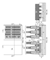
- FIG. 5A is a top-down view of the first exemplary semiconductor structure after formation of fin stack structures according to the first embodiment of the present disclosure.
- FIG. 5B is a vertical cross-sectional view of the first exemplary semiconductor structure along the vertical plane B-B′ of FIG. 5A .
- FIG. 5C is a vertical cross-sectional view of the first exemplary semiconductor structure along the vertical plane C-C′ of FIG. 5A .
- FIG. 6A is a top-down view of the first exemplary semiconductor structure after formation of a shallow trench isolation structure according to the first embodiment of the present disclosure.
- FIG. 6B is a vertical cross-sectional view of the first exemplary semiconductor structure along the vertical plane B-B′ of FIG. 6A .
- FIG. 6C is a vertical cross-sectional view of the first exemplary semiconductor structure along the vertical plane C-C′ of FIG. 6A .
- FIG. 7A is a top-down view of the first exemplary semiconductor structure after recessing the shallow trench isolation structure according to the first embodiment of the present disclosure.
- FIG. 7B is a vertical cross-sectional view of the first exemplary semiconductor structure along the vertical plane B-B′ of FIG. 7A .
- FIG. 7C is a vertical cross-sectional view of the first exemplary semiconductor structure along the vertical plane C-C′ of FIG. 7A .
- FIG. 8A is a top-down view of the first exemplary semiconductor structure after formation of gate stack structures according to the first embodiment of the present disclosure.
- FIG. 8B is a vertical cross-sectional view of the first exemplary semiconductor structure along the vertical plane B-B′ of FIG. 8A .
- FIG. 8C is a vertical cross-sectional view of the first exemplary semiconductor structure along the vertical plane C-C′ of FIG. 8A .
- FIG. 9A is a top-down view of the first exemplary semiconductor structure after formation of a first dielectric masking layer and first gate spacers according to the first embodiment of the present disclosure.
- FIG. 9B is a vertical cross-sectional view of the first exemplary semiconductor structure along the vertical plane B-B′ of FIG. 9A .
- FIG. 9C is a vertical cross-sectional view of the first exemplary semiconductor structure along the vertical plane C-C′ of FIG. 9A .
- FIG. 10A is a top-down view of the first exemplary semiconductor structure after removing physically exposed portions of first-type third semiconductor material fin portions according to the first embodiment of the present disclosure.
- FIG. 10B is a vertical cross-sectional view of the first exemplary semiconductor structure along the vertical plane B-B′ of FIG. 10A .
- FIG. 10C is a vertical cross-sectional view of the first exemplary semiconductor structure along the vertical plane C-C′ of FIG. 10A .
- FIG. 11A is a top-down view of the first exemplary semiconductor structure after formation of a first embedded source region and a first embedded drain region according to the first embodiment of the present disclosure.
- FIG. 11B is a vertical cross-sectional view of the first exemplary semiconductor structure along the vertical plane B-B′ of FIG. 11A .
- FIG. 11C is a vertical cross-sectional view of the first exemplary semiconductor structure along the vertical plane C-C′ of FIG. 11A .
- FIG. 12A is a top-down view of the first exemplary semiconductor structure after formation of a second dielectric masking layer and second gate spacers according to the first embodiment of the present disclosure.
- FIG. 12B is a vertical cross-sectional view of the first exemplary semiconductor structure along the vertical plane B-B′ of FIG. 12A .
- FIG. 12C is a vertical cross-sectional view of the first exemplary semiconductor structure along the vertical plane C-C′ of FIG. 12A .
- FIG. 13A is a top-down view of the first exemplary semiconductor structure after formation of a second embedded source region and a second embedded drain region according to the first embodiment of the present disclosure.
- FIG. 13B is a vertical cross-sectional view of the first exemplary semiconductor structure along the vertical plane B-B′ of FIG. 13A .
- FIG. 13C is a vertical cross-sectional view of the first exemplary semiconductor structure along the vertical plane C-C′ of FIG. 13A .
- FIG. 14A is a top-down view of the first exemplary semiconductor structure after formation of a contact-level dielectric layer and contact via structures according to the first embodiment of the present disclosure.
- FIG. 14B is a vertical cross-sectional view of the first exemplary semiconductor structure along the vertical plane B-B′ of FIG. 14A .
- FIG. 14C is a vertical cross-sectional view of the first exemplary semiconductor structure along the vertical plane C-C′ of FIG. 14A .
- FIG. 15A is a top-down view of a second exemplary semiconductor structure after formation of a silicon-germanium alloy layer and implantation of p-type dopants and n-type dopants according to a second embodiment of the present disclosure.
- FIG. 15B is a vertical cross-sectional view of the second exemplary semiconductor structure along the vertical plane B-B′ of FIG. 15A .
- FIG. 16A is a top-down view of the second exemplary semiconductor structure after formation of a contact-level dielectric layer and contact via structures according to the second embodiment of the present disclosure.
- FIG. 16B is a vertical cross-sectional view of the second exemplary semiconductor structure along the vertical plane B-B′ of FIG. 16A .
- FIG. 16C is a vertical cross-sectional view of the second exemplary semiconductor structure along the vertical plane C-C′ of FIG. 16A .
- the present disclosure relates to semiconductor fins electrically isolated from an underlying semiconductor layer by a well trapping fin portion and a method of manufacturing the same.
- a first exemplary semiconductor structure includes a bulk semiconductor substrate including a first semiconductor material throughout.
- the first semiconductor material can be, for example, single crystalline silicon, a single crystalline silicon-germanium alloy, or a single crystalline silicon-carbon alloy.
- the bulk semiconductor substrate includes a first semiconductor material layer 10 , which can have a p-type doping or an n-type doping.
- a doped well 20 can be formed in an upper portion of the bulk semiconductor substrate such that the doped well has a doping of the opposite conductivity type relative to the doping of the first semiconductor material layer.
- the doped well 20 has an n-type doping, and vice versa.
- the doped well 20 is a first semiconductor material portion, i.e., a portion including the first semiconductor material.
- the first semiconductor material can consist of silicon and a p-type dopant or can consist of silicon and an n-type dopant. In one embodiment, the first semiconductor material does not include germanium or carbon. In one embodiment, the entirety of the first semiconductor material layer 10 and the doped well 20 can be single crystalline with epitaxial alignment throughout.
- the first exemplary semiconductor structure includes a first device region DR 1 and a second device region DR 2 .
- a top surface of the first semiconductor material layer 10 in the entirety of the first device region DR 1 , and the doped well 20 can be provided in the second device region DR 2 .
- a top surface of a p-doped semiconductor region can be provided in the first device region DR 1
- a top surface of an n-doped semiconductor region can be provided in the second device region DR 2 .
- the first semiconductor material layer 10 can include p-doped single crystalline silicon and a top surface of the first semiconductor material layer 10 can be physically exposed in the first device region DR 1
- the doped well 20 can include n-doped single crystalline silicon and a top surface of the doped well can be physically exposed in the second device region DR 2
- the doped well 20 can be provided in the first device region DR 1 and can include p-doped single crystalline silicon of which a top surface is physically exposed
- the first semiconductor material layer 10 can include an n-doped single crystalline silicon and have a physically exposed top surface within the second device region DR 2 .
- a silicon-carbon alloy layer 16 L is formed on a p-doped semiconductor region, and a silicon-germanium alloy layer 26 L is formed on an n-doped semiconductor region.
- the silicon-carbon alloy layer 16 L is selected on the top surface of the p-doped semiconductor region selected from the first semiconductor material layer 10 and the doped well 20
- the silicon-germanium alloy layer 26 L is formed on the top surface of the n-doped semiconductor region selected from the first semiconductor material layer 10 and the doped well 20 .
- the silicon-carbon alloy layer 16 L and the silicon-germanium alloy layer 26 L can be formed sequentially.
- the silicon-carbon alloy layer 16 L may be formed prior to, or after, formation of the silicon-germanium alloy layer 26 L.
- the top surface of the n-doped semiconductor region i.e., one of the first semiconductor material layer 10 and the doped well 20
- a dielectric masking material layer such as a silicon oxide layer or a silicon nitride layer
- silicon-carbon alloy layer 16 L can be formed as an intrinsic (undoped) single crystalline silicon-carbon alloy layer. The dielectric masking layer is subsequently removed.
- the top surface of the p-doped semiconductor region i.e., the other of the first semiconductor material layer 10 and the doped well 20
- a dielectric masking material layer such as a silicon oxide layer or a silicon nitride layer
- deposition of a silicon-germanium alloy material occurs on the top surface of the n-doped semiconductor region.
- Selective epitaxy can be employed to deposit the silicon-germanium alloy on the n-doped semiconductor region, while the silicon-germanium alloy material does not grow on dielectric surfaces.
- the silicon-germanium alloy layer 26 L can be formed as an intrinsic (undoped) single crystalline silicon-germanium alloy layer. The dielectric masking layer is subsequently removed.
- the silicon-carbon alloy layer 16 L can have an atomic concentration of carbon in a range from 0.1% to 2.0%, the atomic concentration of silicon being the balance.
- the silicon-germanium alloy layer 26 L can have an atomic concentration of germanium in a range from 1% to 80%, the atomic concentration of silicon being the balance.
- the thickness of the silicon-carbon alloy layer 16 L can be in a range from 10 nm to 100 nm, although lesser and greater thicknesses can also be employed.
- the thickness of the silicon-germanium alloy layer 26 L can be in a range from 10 nm to 100 nm, although lesser and greater thicknesses can also be employed.
- the material of the silicon-carbon alloy layer 16 L or the material of the silicon-germanium alloy layer 26 L is referred to as a second semiconductor material.
- the first semiconductor material is p-doped
- the second semiconductor material is a silicon-carbon alloy material.
- the first semiconductor material is n-doped
- the second semiconductor material is a silicon-germanium alloy material.
- n-type dopants are introduced into the silicon-carbon alloy layer 16 L employing a masked ion implantation process, and p-type dopants are introduced into the silicon-germanium alloy layer 26 L employing another masked ion implantation process.
- the species of the n-dopant is selected such that the n-type dopants implanted into the silicon-carbon alloy layer 16 L have a lesser diffusivity in the silicon-carbon alloy layer 16 L than in the underlying p-doped semiconductor material region, i.e., one of the first semiconductor material of the first semiconductor material layer 10 and the doped well 20 that is present in the first device region DR 1 .
- the species of the p-dopant is selected such that the p-type dopants implanted into the silicon-germanium alloy layer 26 L have a lesser diffusivity in the silicon-germanium alloy layer 26 L than in the underlying n-doped semiconductor material region, i.e., the other of the first semiconductor material of the first semiconductor material layer 10 and the doped well 20 that is present in the second device region DR 2 .
- the conductivity type of the implanted dopants is referred to as a first conductivity type.
- the first conductivity type is n-type.
- the second conductivity type is p-type.
- the dopant of the first conductivity type has a lesser diffusivity in the second semiconductor material (which is the silicon-carbon alloy material in the first device region DR 1 and the silicon-germanium alloy material in the second device region DR 2 ) than in the first semiconductor material.
- each second semiconductor material layer (which is the silicon-carbon alloy layer 16 L in the first device region DR 1 and the silicon-germanium alloy layer 26 L in the second device region DR 2 ) functions as a trapping well that provides electrical isolation via a p-n junction for a semiconductor material portion to be subsequently deposited thereupon.
- each second semiconductor material layer ( 16 L, 26 L) is herein referred to as a well trapping layer, i.e., a layer that functions as a well providing trapping of electrical charges provided by leakage current, thereby providing electrical isolation of the semiconductor material portion to be subsequently formed.
- the well trapping layer is the silicon-carbon alloy layer 16 .
- the well trapping layer is the silicon-germanium alloy layer 26 .
- the entirety of each well trapping layer ( 16 L or 26 L) includes the second semiconductor material for the corresponding device region (DR 1 or DR 2 ).
- an ion implantations process can be performed in the first device region DR 1 such that the n-type dopants are implanted into a middle portion of the silicon-carbon alloy layer 16 L.
- the middle portion of the silicon-carbon alloy layer 16 L in which the concentration of the implanted n-type dopants is in a range between 10% of the peak atomic concentration and 100% of the peak atomic concentration is herein referred to as an n-doped silicon-carbon alloy layer 14 L, which is a doped semiconductor material region including the silicon-carbon alloy material (that is the second semiconductor material within the first device region DR 1 ) and the n-type dopant (that is the first conductivity type dopant within the first device region DR 1 ).
- the n-type dopant is arsenic or phosphorus.
- the n-type dopant has a lesser diffusivity in the silicon-carbon alloy material than in the first semiconductor material in the first device region DR 1 (which can be silicon).
- An upper silicon-carbon alloy layer 15 L formed above the n-doped silicon-carbon alloy layer 14 L has a vertical dopant concentration that exponentially decreases with a vertical distance from the interface with the n-doped silicon-carbon alloy layer 14 L.
- a lower silicon-carbon alloy layer 13 L formed below the n-doped silicon-carbon alloy layer 14 L has a vertical dopant concentration that exponentially decreases with a vertical distance from the interface with the n-doped silicon-carbon alloy layer 14 L.
- the thickness of the n-doped silicon-carbon alloy layer 14 L increases, and the thicknesses of the upper and lower silicon-carbon alloy regions ( 15 L, 13 L) decrease.
- the thickness of the n-doped silicon-carbon alloy layer 14 L can be in a range from 10% to 80% of the thickness of the silicon-carbon alloy layer 16 L.
- the peak atomic concentration of the n-type dopants in the n-doped silicon-carbon alloy layer 14 L can be in a range from 1.0 ⁇ 10 17 /cm 3 to 1.0 ⁇ 10 20 /cm 3 , although lesser and greater peak concentrations can also be employed.
- another ion implantations process can be performed in the second device region DR 2 such that the p-type dopants are implanted into a middle portion of the silicon-germanium alloy layer 26 L.
- the middle portion of the silicon-germanium alloy layer 26 L in which the concentration of the implanted p-type dopants is in a range between 10% of the peak atomic concentration and 100% of the peak atomic concentration is herein referred to as a p-doped silicon-germanium alloy layer 24 L, which is a doped semiconductor material region including the silicon-germanium alloy material (that is the second semiconductor material within the second device region DR 2 ) and the p-type dopant (that is the first conductivity type dopant within the second device region DR 2 ).
- the p-type dopant is boron.
- the p-type dopant has a lesser diffusivity in the silicon-germanium alloy material than in the first semiconductor material in the second device region DR 2 (which can be silicon).
- An upper silicon-germanium alloy layer 25 L formed above the p-doped silicon-germanium alloy layer 24 L has a vertical dopant concentration that exponentially decreases with a vertical distance from the interface with the p-doped silicon-germanium alloy layer 24 L.
- a lower silicon-germanium alloy layer 23 L formed below the p-doped silicon-germanium alloy layer 24 L has a vertical dopant concentration that exponentially decreases with a vertical distance from the interface with the p-doped silicon-germanium alloy layer 24 L.
- the thickness of the p-doped silicon-germanium alloy layer 24 L increases, and the thicknesses of the upper and lower silicon-germanium alloy layers ( 25 L, 23 L) decrease.
- the thickness of the p-doped silicon-germanium alloy layer 24 L can be in a range from 10% to 80% of the thickness of the silicon-germanium alloy layer 26 L.
- the peak atomic concentration of the p-type dopants in the p-doped silicon-germanium alloy layer 24 L can be in a range from 1.0 ⁇ 10 17 /cm 3 to 1.0 ⁇ 10 20 /cm 3 , although lesser and greater peak concentrations can also be employed.
- a semiconductor material layer is formed in each of the first device region DR 1 and the second device region DR 2 .
- the material of the semiconductor material layer is herein referred to as a third semiconductor material.
- a first-type third semiconductor material layer 18 L is formed in the first device region DR 1
- a second-type third semiconductor material layer 28 L is formed in the second device region DR 2 .
- the thickness of each of the first-type third semiconductor material layer 18 L and the second-type third semiconductor material layer 28 L can be in a range from 30 nm to 300 nm, although lesser and greater thicknesses can also be employed.
- the first-type third semiconductor material layer 18 L can be intrinsic, or can have an n-type doping at a dopant concentration in a range from 1.0 ⁇ 10 14 /cm 3 to 1.0 ⁇ 10 18 /cm 3 , although lesser and greater peak concentrations can also be employed.
- the second-type third semiconductor material layer 28 L can be intrinsic, or can have a p-type doping at a dopant concentration in a range from 1.0 ⁇ 10 14 /cm 3 to 1.0 ⁇ 10 18 /cm 3 , although lesser and greater peak concentrations can also be employed.
- the third semiconductor material of each device region can be formed, for example, by epitaxial deposition of the third semiconductor material.
- the third semiconductor material for the first device region DR 1 is selected such that the n-type dopants in the silicon-carbon alloy layer 16 L have a lesser diffusivity in the silicon-carbon alloy of the silicon-carbon alloy layer 16 L (which is the second semiconductor material of the first device region DR 1 ) than in the first semiconductor material or in the third semiconductor material of the first device region DR 1 .
- the third semiconductor material for the second device region DR 2 is selected such that the p-type dopants in the silicon-germanium alloy layer 26 L have a lesser diffusivity in the silicon-germanium alloy of the silicon-germanium alloy layer 26 L (which is the second semiconductor material of the second device region DR 1 ) than in the first semiconductor material or in the third semiconductor material of the second device region DR 2 .
- the third semiconductor material can be the same across the first and second device regions (DR 1 , DR 2 ).
- a single semiconductor material layer can be epitaxially grown simultaneously on the silicon-carbon alloy layer 16 L and the silicon-germanium alloy layer 26 L.
- the single semiconductor material layer includes the first-type third semiconductor material layer 18 L and the second-type third semiconductor material layer 28 L.
- the first-type third semiconductor material layer 18 L and the second-type third semiconductor material layer 28 L may be intrinsic, or can be doped with p-type dopants and n-type dopants, respectively.
- the first-type third semiconductor material layer 18 L and the second-type third semiconductor material layer 28 L are semiconductor layers in which components of semiconductor devices can be subsequently formed, and as such, are referred to as device semiconductor material layers.
- the dopant of the first conductivity type has a lesser diffusivity in the second semiconductor material (which is the silicon-carbon alloy material in the first device region DR 1 and the silicon-germanium alloy material in the second device region DR 2 ) than in the first semiconductor material, and than in the third semiconductor material (which is the material of the first-type third semiconductor material layer 18 L in the first device region DR 1 , or the material of the second-type third semiconductor material layer 28 L in the second device region DR 2 ).
- At least one dielectric cap layer can be subsequently formed.
- the at least one dielectric cap layer can include a stack of a first dielectric cap layer 32 L and a second dielectric cap layer 34 L can be subsequently formed.
- the first dielectric cap layer 32 L can include silicon oxide having a thickness in a range from 1 nm to 10 nm
- the second dielectric cap layer 34 L can include silicon nitride having a thickness in a range from 3 nm to 60 nm, although lesser and greater thicknesses can also be employed.
- a photoresist material (not shown) is applied over the at least one dielectric cap layer ( 32 L, 34 L), and is lithographically patterned to form patterned photoresist portions (not shown) having horizontal cross-sectional areas of rectangles.
- the pattern of the patterned photoresist portions is transferred through the at least one dielectric cap layer ( 32 L, 34 L) by an anisotropic etch.
- Each dielectric cap stack ( 32 , 34 ) includes a first dielectric cap portion 32 and a second dielectric cap portion 34 .
- the patterned photoresist portions can be optionally removed after patterning of the at least one dielectric cap layer ( 32 L, 34 L) into dielectric cap stacks ( 32 , 34 ).
- an anisotropic etch is employed to transfer the pattern in the dielectric cap stacks ( 32 , 34 ) into the underlying semiconductor layers.
- the underlying semiconductor layers include a third semiconductor material layer, a well trapping layer, and an upper portion of the semiconductor substrate ( 10 , 20 ). Fin stack structures are formed in each device region. Any patterned photoresist portions, if present, can be removed during the anisotropic etch that forms the fin stack structures.
- the underlying semiconductor layers include the first-type third semiconductor material layer 18 L, the silicon-carbon alloy layer 16 L, and the upper portion of one of the first semiconductor material layer 10 and the doped well 20 .
- Each remaining portion of the first-type third semiconductor material layer 18 L is a semiconductor fin portion including the third semiconductor material of the first device region DR 1 , and is herein referred to as a first-type third semiconductor fin portion 18 .
- a “fin portion” refers to a portion having a pair of parallel sidewalls extending along a horizontal direction.
- Each remaining portion of the silicon-carbon alloy layer 16 L includes a first-type well trapping fin portion 16 , which is a fin portion that includes a trapping well and is located within the first device region DR 1 .
- Each first-type well trapping fin portion 16 includes an n-doped silicon-carbon alloy fin portion 14 , an upper silicon-carbon alloy fin portion 15 , and a lower silicon-carbon alloy fin portion 13 .
- Each n-doped silicon-carbon alloy fin portion 14 is a remaining portion of the n-doped silicon-carbon alloy layer 14 L.
- Each upper silicon-carbon alloy fin portion 15 is a remaining portion of the upper silicon-carbon alloy layer 15 L.
- Each lower silicon-carbon alloy fin portion 13 is a remaining portion of the lower silicon-carbon alloy layer 13 L.
- first-type first semiconductor material fin portion 12 Each patterned upper portion of the first semiconductor material region within the first device region is herein referred to as a first-type first semiconductor material fin portion 12 .
- the first-type first semiconductor material fin portion 12 can be a patterned portion of an upper portion of the first semiconductor material layer 10 as provided at the processing steps of FIGS. 1A and 1B , or can be a patterned portion of the upper portion of the doped well 20 as provided at the processing steps of FIGS. 1A and 1B .
- the underlying semiconductor layers include the second-type third semiconductor material layer 28 L, the silicon-germanium alloy layer 26 L, and the upper portion of the other of the first semiconductor material layer 10 and the doped well 20 .
- Each remaining portion of the second-type third semiconductor material layer 28 L is a semiconductor fin portion including the third semiconductor material of the second device region DR 1 , and is herein referred to as a second-type third semiconductor fin portion 28 .
- Each remaining portion of the silicon-germanium alloy layer 26 L includes a second-type well trapping fin portion 26 , which is a fin portion that includes a trapping well and is located within the second device region DR 2 .
- Each second-type well trapping fin portion 26 includes a p-doped silicon-germanium alloy fin portion 24 , an upper silicon-germanium alloy fin portion 25 , and a lower silicon-germanium alloy fin portion 23 .
- Each n-doped silicon-germanium alloy fin portion 24 is a remaining portion of the n-doped silicon-germanium alloy layer 24 L.
- Each upper silicon-germanium alloy fin portion 25 is a remaining portion of the upper silicon-germanium alloy layer 25 L.
- Each lower silicon-germanium alloy fin portion 23 is a remaining portion of the lower silicon-germanium alloy layer 23 L.
- Each patterned upper portion of the first semiconductor material region within the second device region is herein referred to as a second-type first semiconductor material fin portion 22 .
- the first-type first semiconductor material fin portion 22 can be a patterned portion of a patterned portion of the upper portion of the doped well 20 as provided at the processing steps of FIGS. 2A and 2B , or can be an upper portion of the first semiconductor material layer 20 as provided at the processing steps of FIGS. 2A and 2B .
- the fin stack structures in the first device region DR 1 are herein referred to as first-type fin stack structures.
- the fin stack structures in the second device region DR 2 are herein referred to as second-type fin stack structures.
- Each fin stack structure has a pair of substantially vertical parallel sidewalls, and is located on an unpatterned portion of the semiconductor substrate ( 10 , 20 ).
- the horizontal cross-sectional shape of each fin stack structure can be substantially the same irrespective of the height of the cross-section. As used herein, two shapes are substantially the same if the difference between two shapes is less than twice the surface roughness at the atomic level.
- Each fin stack structure includes a first semiconductor material fin portion, a well trapping fin portion, and a third semiconductor material fin portion.
- the first semiconductor material fin portion includes the first semiconductor material and is located over the semiconductor substrate ( 10 , 20 ).
- the well trapping fin portion includes the second semiconductor material of the corresponding device region, is located over the first semiconductor material fin portion, and contains a doped semiconductor material region that includes the second semiconductor material and a dopant of the first conductivity type for the corresponding device region.
- the doped semiconductor material region laterally extends throughout the area of the fin stack structure.
- the third semiconductor material fin portion includes the third semiconductor material for the corresponding region, and is located over the well trapping fin portion.
- each first-type fin stack structure ( 12 , 16 , 18 ) includes a first-type first semiconductor material fin portion 12 , a first-type well trapping fin portion 16 , and a first-type third semiconductor material fin portion 18 .
- the first-type first semiconductor material fin portion 12 includes the first semiconductor material and is located over the semiconductor substrate ( 10 , 20 ).
- the first-type well trapping fin portion 16 includes the second semiconductor material of the first device region DR 1 , is located over the first-type first semiconductor material fin portion 12 , and contains an n-doped silicon-carbon alloy fin portion 14 .
- the n-doped silicon-carbon alloy fin portion 14 is a doped semiconductor material region that includes the second semiconductor material and an n-type dopant, which is the dopant of the first conductivity type for the first device region DR 1 .
- the n-doped silicon-carbon alloy fin portion 14 laterally extends throughout the area of the first-type fin stack structure ( 12 , 16 , 18 ).
- the first-type third semiconductor material fin portion 18 includes the third semiconductor material for the first device region DR 1 , and is located over the first-type well trapping fin portion 16 .
- each first-type fin stack structure ( 12 , 16 , 18 ) the sidewalls of the first-type first semiconductor material fin portion 12 , the first-type well trapping fin portion 16 , and the first-type third semiconductor material fin portion 18 are vertically coincident among one another.
- two surfaces are vertically coincident if there exists a vertical surface from which each of the two surfaces deviates by no more than the surface roughness of the respective surface.
- Each second-type fin stack structure ( 22 , 26 , 28 ) includes a second-type first semiconductor material fin portion 22 , a second-type well trapping fin portion 26 , and a second-type third semiconductor material fin portion 28 .
- the second-type first semiconductor material fin portion 22 includes the first semiconductor material and is located over the semiconductor substrate ( 10 , 20 ).
- the second-type well trapping fin portion 26 includes the second semiconductor material of the second device region DR 2 , is located over the second-type first semiconductor material fin portion 22 , and contains a p-doped silicon-germanium alloy fin portion 24 .
- the p-doped silicon-germanium alloy fin portion 24 is a doped semiconductor material region that includes the second semiconductor material and a p-type dopant, which is the dopant of the first conductivity type for the second device region DR 2 .
- the p-doped silicon-germanium alloy fin portion 24 laterally extends throughout the area of the second-type fin stack structure ( 22 , 26 , 28 ).
- the second-type third semiconductor material fin portion 28 includes the third semiconductor material for the second device region DR 2 , and is located over the second-type well trapping fin portion 26 .
- each second-type fin stack structure 22 , 26 , 28 ) the sidewalls of the second-type first semiconductor material fin portion 22 , the second-type well trapping fin portion 26 , and the second-type third semiconductor material fin portion 28 are vertically coincident among one another.
- a dielectric material such as silicon oxide is deposited over the dielectric cap stacks ( 32 , 34 ), the first-type fin stack structures ( 12 , 16 , 18 ), and the second-type fin stack structures ( 22 , 26 , 28 ).
- the deposited dielectric material is subsequently planarized, for example, by chemical mechanical planarization to form a shallow trench isolation structure 30 that laterally surrounds each of the first-type fin stack structures ( 12 , 16 , 18 ) and the second-type fin stack structures ( 22 , 26 , 28 ).
- the top surface of the dielectric cap stacks ( 32 , 34 ) can be employed as stopping surfaces for the planarization process.
- the shallow trench isolation structure 30 is recessed by an etch below the top surfaces of the first-type fin stack structures ( 12 , 16 , 18 ) and the second-type fin stack structures ( 22 , 26 , 28 ). Sidewall surfaces of the third semiconductor material fin portions ( 18 , 28 ) are physically exposed.
- the recessed top surface of the shallow trench isolation structure 30 can be substantially coplanar with the interface between the first-type well trapping fin portion 16 and the first-type third semiconductor material fin portion 18 and/or with the interface between the second-type well trapping fin portion 26 and the second-type third semiconductor material fin portion 28 .
- gate stack structures can be formed along the widthwise direction of each fin stack structure ( 12 , 16 , 18 ; 22 , 26 , 28 ).
- a widthwise direction is a horizontal direction that is perpendicular to the lengthwise direction.
- Each gate stack structure includes a vertical stack, from bottom to top, of a gate dielectric 50 , a gate electrode 52 , and a gate cap dielectric 58 .
- the gate stack structures ( 50 , 52 , 58 ) can be formed, for example, by formation of a gate material layer stack including a gate dielectric layer, a gate electrode layer including at least one conductive material, and a gate cap dielectric layer including a dielectric material, and by patterning the gate material layer stack by a combination of lithographic methods and at least one anisotropic etch.
- a plurality of gate stack structures ( 50 , 52 , 58 ) may straddle a fin stack structure ( 12 , 16 , 18 ; or 22 , 26 , 28 ).
- One or more gate stack structures can straddle each fin stack structure ( 12 , 16 , 18 ; or 22 , 26 , 28 ).
- a gate dielectric 50 may contact the entirety of an end wall of a third semiconductor material fin portions ( 18 or 28 ).
- a first dielectric masking layer 54 L is deposited over the first exemplary semiconductor structure by a conformal deposition method such as low pressure chemical vapor deposition (LPCVD).
- LPCVD low pressure chemical vapor deposition
- the portion of the first dielectric masking layer 54 L in the second device region DR 2 can be masked by a patterned photoresist layer (not shown), while the portion of the first dielectric masking layer 54 L is physically exposed in the first device region DR 1 .
- first dielectric masking layer 54 L While the patterned photoresist layer protects the portion of the first dielectric masking layer 54 L in the second device region DR 2 , horizontal portions of the first dielectric masking layer 54 L in the first device region DR 1 can be removed by an anisotropic etch that employs the patterned photoresist layer as an etch mask. The remaining vertical portions of the first dielectric masking layer 54 L forms first gate spacers 54 . Each first gate spacer 54 laterally surrounds a gate stack structure ( 50 , 52 , 58 ). The patterned photoresist layer can be removed, for example, by ashing.
- a source region and a drain region can be formed on the first-type fin stack structures ( 12 , 16 , 18 ). Specifically, the source region and the drain region can be formed in the sub-portions of the first-type third semiconductor material fin portion 18 that are not covered by the gate stack structures ( 50 , 52 , 58 ) or the first gate spacers 54 .
- physically exposed portions of the first-type third semiconductor material fin portion 18 can be removed, for example, by an anisotropic etch in an exemplary processing sequence. Regions of the third semiconductor material from the first-type fin stack structures ( 12 , 16 , 18 ) are removed employing the first gate spacers 18 and the gate stack structure ( 50 , 52 , 58 ) as an etch mask. In one embodiment, the third semiconductor material of the first device region DR 1 can be etched employing the top surfaces of the first-type well trapping fin portion 16 as an etch stop surfaces or as endpoint surfaces.
- each first-type fin stack structure 12 , 16 , 18 .
- the remaining portion of each first-type third semiconductor material fin portion 18 as provided at the end of the processing steps of FIGS. 9A-9C includes a plurality of third semiconductor material fin portions 18 after the processing steps of FIGS. 10A-10C .
- first embedded source region 32 and a first embedded drain region 38 can be formed by depositing an additional semiconductor material in the at least one source side cavity 31 and the at least one drain side cavity 37 .
- the additional semiconductor material that forms the first embedded source region 32 and a first embedded drain region 38 can be deposited, for example, by selective epitaxy, in which the additional semiconductor material grows on semiconductor surfaces and does not grow on dielectric surfaces.
- the first embedded source region 32 and the first embedded drain region 38 can be doped with dopants of the opposite conductivity type as the first conductivity type for the first device region DR 1 .
- the opposite conductivity type of the first conductivity type is herein referred to as a second conductivity type in each device region.
- the first conductivity type is n-type and the second conductivity type is p-type in the first device region DR 1
- the first conductivity type is p-type and the second conductivity type is n-type in the second device region DR 2
- the first embedded source region 32 and the first embedded drain region 38 can be doped by in-situ doping, or can be doped by ion implantation.
- the first embedded source region 32 and the first embedded drain region 38 can extend across a plurality of first-type fin stack structures ( 12 , 16 , 18 ) along a direction parallel to the lengthwise direction of the gate stack structures ( 50 , 52 , 58 ) in the first device region DR 1 .
- a second dielectric masking layer 56 L is deposited over the first exemplary semiconductor structure by a conformal deposition method such as a low pressure chemical vapor deposition (LPCVD).
- LPCVD low pressure chemical vapor deposition
- the portion of the second dielectric masking layer 56 L in the first device region DR 1 can be masked by a patterned photoresist layer (not shown), while the portion of the second dielectric masking layer 56 L is physically exposed in the second device region DR 2 .
- the patterned photoresist layer protects the portion of the second dielectric masking layer 56 L in the first device region DR 1
- horizontal portions of the second dielectric masking layer 56 L in the second device region DR 2 can be removed by an anisotropic etch that employs the patterned photoresist layer as an etch mask.
- the remaining vertical portions of the second dielectric masking layer 56 L forms second gate spacers 56 .
- Each second gate spacer 56 laterally surrounds a gate stack structure ( 50 , 52 , 58 ).
- the patterned photoresist layer can be removed, for example, by ashing.
- a source region and a drain region can be formed on the second-type fin stack structures ( 22 , 26 , 28 ). Specifically, the source region and the drain region can be formed in the sub-portions of the second-type third semiconductor material fin portion 28 that are not covered by the gate stack structures ( 50 , 52 , 58 ) or the second gate spacers 54 .
- physically exposed portions of the second-type third semiconductor material fin portion 28 can be removed, for example, by an anisotropic etch in an exemplary processing sequence. Regions of the third semiconductor material from the second-type fin stack structures ( 22 , 26 , 28 ) are removed employing the second gate spacers 28 and the gate stack structure ( 50 , 52 , 58 ) as an etch mask. In one embodiment, the third semiconductor material of the second device region DR 2 can be etched employing the top surfaces of the second-type well trapping fin portion 26 as an etch stop surfaces or as endpoint surfaces.
- each second-type fin stack structure 22 , 26 , 28 .
- the remaining portion of each second-type third semiconductor material fin portion 28 as provided at the end of the processing steps of FIGS. 12A-12C can become a plurality of third semiconductor material fin portions 28 .
- Second embedded source region 42 and a second embedded drain region 48 can be formed by depositing an additional semiconductor material in the at least one source side cavity and the at least one drain side cavity.
- the additional semiconductor material that forms the second embedded source region 42 and a second embedded drain region 48 can be deposited, for example, by selective epitaxy, in which the additional semiconductor material grows on semiconductor surfaces and does not grow on dielectric surfaces.
- the second embedded source region 42 and the second embedded drain region 48 can be doped with dopants of the opposite conductivity type as the first conductivity type for the second device region DR 2 .
- the first conductivity type is p-type and the second conductivity type is n-type in the second device region DR 2 .
- the second embedded source region 42 and the second embedded drain region 48 can be doped by in-situ doping, or can be doped by ion implantation.
- the second embedded source region 42 and the second embedded drain region 48 can extend across a plurality of second-type fin stack structures ( 22 , 26 , 28 ) along a direction parallel to the lengthwise direction of the gate stack structures ( 50 , 52 , 58 ) in the second device region DR 2 .
- a contact-level dielectric layer 80 can be subsequently deposited over the first exemplary semiconductor structure.
- the contact-level dielectric layer 80 includes a dielectric material such as porous or non-porous organosilicate glass (OSG), silicon oxide, silicon nitride, or a combination thereof.
- the top surface of the contact-level dielectric layer 80 can be planarized, for example, by chemical mechanical planarization.
- Various contact via structures are formed through the contact-level dielectric layer 80 employing methods known in the art.
- the various contact via structures can include, for example, source contact via structures 82 , gate contact via structures 85 , and drain side contact via structures 88 .
- a second exemplary semiconductor structure according to a second embodiment of the present disclosure can be derived from the first exemplary semiconductor structure of FIGS. 1A and 1B by employing a silicon-germanium alloy layer across the entirety of the first device region DR 1 and the second device region DR 2 in lieu of a combination of a silicon-carbon alloy layer 16 L and a silicon-germanium alloy layer 26 L illustrated in FIGS. 2A and 2B .
- the silicon-germanium alloy layer of the second embodiment is formed on the top surface of a p-doped semiconductor region and an n-doped semiconductor region.
- One of the p-doped semiconductor region and the n-doped semiconductor region is the first semiconductor material layer 10
- the other of the p-doped semiconductor region and the n-doped semiconductor region is the doped well 20 .
- Non-selective or selective epitaxy can be employed to form the silicon-germanium alloy layer of the second embodiment.
- the silicon-germanium alloy layer can be formed as an intrinsic (undoped) single crystalline silicon-germanium alloy layer.
- the silicon-germanium alloy layer can have an atomic concentration of germanium in a range from 1% to 80%, the atomic concentration of silicon being the balance.
- the thickness of the silicon-germanium alloy layer 26 L can be in a range from 10 nm to 100 nm, although lesser and greater thicknesses can also be employed.
- the material of the silicon-germanium alloy layer 26 L, i.e., the silicon-germanium alloy is the second semiconductor material for the first device region DR 1 and the second device region DR 2 .
- N-type dopants are introduced into the portion of the silicon-germanium layer in the first device region DR 1 employing a masked ion implantation process.
- P-type dopants are introduced into the portion of the silicon-germanium alloy layer in the second device region DR 2 employing another masked ion implantation process.
- the species of the n-dopant is selected such that the n-type dopants implanted into the silicon-germanium layer has a lesser diffusivity in the silicon-germanium alloy layer than in the underlying p-doped semiconductor material region, i.e., one of the first semiconductor material of the first semiconductor material layer 10 and the doped well 20 that is present in the first device region DR 1 .
- the species of the p-dopant is selected such that the p-type dopants implanted into the silicon-germanium alloy layer has a lesser diffusivity in the silicon-germanium alloy layer than in the underlying n-doped semiconductor material region, i.e., the other of the first semiconductor material of the first semiconductor material layer 10 and the doped well 20 that is present in the second device region DR 2 .
- the conductivity type of the implanted dopants is referred to as a first conductivity type.
- the first conductivity type is n-type.
- the second conductivity type is p-type.
- the dopant of the first conductivity type has a lesser diffusivity in the second semiconductor material, i.e., in the silicon-germanium alloy material, than in the first semiconductor material.
- the second semiconductor material layer (which is the silicon-germanium alloy layer) functions a trapping well that provides electrical isolation via a p-n junction for a semiconductor material portion to be subsequently deposited thereupon.
- the second semiconductor material layer is herein referred to as a well trapping layer, i.e., a layer that functions as a well providing trapping of electrical charges provided by leakage current, thereby providing electrical isolation of the semiconductor material portion to be subsequently formed.
- the entirety of each well trapping layer includes the second semiconductor material, i.e., the silicon-germanium alloy.
- an ion implantations process can be performed in the first device region DR 1 such that the n-type dopants are implanted into a middle portion of the silicon-carbon alloy layer.
- the middle portion of the silicon-carbon alloy layer in which the concentration of the implanted n-type dopants is in a range between 10% of the peak atomic concentration and 100% of the peak atomic concentration is herein referred to as an n-doped silicon-germanium alloy layer 94 L, which is a doped semiconductor material region including the silicon-germanium alloy material (that is the second semiconductor material) and the n-type dopant (that is the first conductivity type dopant within the first device region DR 1 ).
- the n-type dopant is arsenic.
- the n-type dopant has a lesser diffusivity in the silicon-germanium alloy material than in the first semiconductor material in the first device region DR 1 (which can be silicon).
- another ion implantations process can be performed in the second device region DR 2 such that the p-type dopants are implanted into a middle portion of the silicon-germanium alloy layer.
- the middle portion of the silicon-germanium alloy layer in which the concentration of the implanted p-type dopants is in a range between 10% of the peak atomic concentration and 100% of the peak atomic concentration is herein referred to as a p-doped silicon-germanium alloy layer 24 L, which is a doped semiconductor material region including the silicon-germanium alloy material (that is the second semiconductor material) and the p-type dopant (that is the first conductivity type dopant within the second device region DR 2 ).
- the p-type dopant is boron.
- the p-type dopant has a lesser diffusivity in the silicon-germanium alloy material than in the first semiconductor material in the second device region DR 2 (which can be silicon).
- An upper silicon-germanium alloy layer 25 L is present above the n-doped silicon-germanium alloy layer 94 L and the p-doped silicon-germanium alloy layer 24 L.
- the upper silicon-germanium alloy layer 25 L has a vertical dopant concentration of p-type dopants or n-type dopants that exponentially decreases with a vertical distance from the interface with the n-doped silicon-germanium alloy layer 94 L or the p-doped silicon-germanium alloy layer 24 L.
- a lower silicon-germanium alloy layer 23 L formed below the n-doped silicon-germanium alloy layer 94 L and the p-doped silicon-germanium alloy layer 24 L.
- the lower silicon-germanium alloy layer 23 L has a vertical dopant concentration that exponentially decreases with a vertical distance from the interface with the n-doped silicon-germanium alloy layer 94 L or the p-doped silicon-germanium alloy layer 24 L.
- the thicknesses of the n-doped silicon-germanium alloy layer 94 L and the p-doped silicon-germanium alloy layer 24 L increase, and the thicknesses of the upper and lower silicon-germanium alloy layers ( 25 L, 23 L) decrease.
- the thickness of the n-doped silicon-germanium alloy layer 94 L can be in a range from 10% to 80% of the thickness of the silicon-carbon alloy layer 16 L.
- the peak atomic concentration of the n-type dopants in the n-doped silicon-germanium alloy layer 94 L can be in a range from 1.0 ⁇ 10 17 /cm 3 to 1.0 ⁇ 10 20 /cm 3 , although lesser and greater peak concentrations can also be employed.
- the thickness of the p-doped silicon-germanium alloy layer 24 L can be in a range from 10% to 80% of the thickness of the silicon-germanium alloy layer 26 L.
- the peak atomic concentration of the p-type dopants in the p-doped silicon-germanium alloy layer 24 L can be in a range from 1.0 ⁇ 10 17 /cm 3 to 1.0 ⁇ 10 20 /cm 3 , although lesser and greater peak concentrations can also be employed.
- the silicon-germanium alloy layer includes the n-doped silicon-germanium alloy layer 94 L, the p-doped silicon-germanium alloy layer 24 L, the upper silicon-germanium alloy layer 25 L, and the lower silicon-germanium alloy layer 23 L.
- FIGS. 4A and 4B, 5A-5C, 6A-6C, 7A-7C, 8A-8C, 9A-9C, 10A-10C, 11A-11C, 12A-12C, 13A-13C, and 14A - 14 C can be subsequently performed to provide the second exemplary semiconductor structure shown in FIGS. 16A-16C .
- each first-type well trapping fin portion 16 ′ of the second embodiment replaces a first-type well trapping fin portion 16 of the first embodiment.
- first-type well trapping fin portion 16 ′ is a fin portion that includes a trapping well and is located within the first device region DR 1 .
- Each first-type well trapping fin portion 16 ′ includes an n-doped silicon-germanium alloy fin portion 94 , an upper silicon-germanium alloy fin portion 25 , and a lower silicon-germanium alloy fin portion 23 .
- Each n-doped silicon-germanium alloy fin portion 94 is a remaining portion of the n-doped silicon-germanium alloy layer 94 L.
- Each upper silicon-germanium alloy fin portion 25 is a remaining portion of the upper silicon-germanium alloy layer 25 L.
- Each lower silicon-germanium alloy fin portion 23 is a remaining portion of the lower silicon-germanium alloy layer 23 L.
- Each patterned upper portion of the first semiconductor material region within the first device region is herein referred to as a first-type first semiconductor material fin portion 12 .
- the first-type first semiconductor material fin portion 12 can be a patterned portion of an upper portion of the first semiconductor material layer 10 , or can be a patterned portion of the upper portion of the doped well 20 .
Abstract
Description
Claims (13)
Priority Applications (2)
| Application Number | Priority Date | Filing Date | Title |
|---|---|---|---|
| US14/510,650 US9496258B2 (en) | 2013-03-11 | 2014-10-09 | Semiconductor fin isolation by a well trapping fin portion |
| US15/331,351 US10242980B2 (en) | 2013-03-11 | 2016-10-21 | Semiconductor fin isolation by a well trapping fin portion |
Applications Claiming Priority (2)
| Application Number | Priority Date | Filing Date | Title |
|---|---|---|---|
| US13/792,797 US8933528B2 (en) | 2013-03-11 | 2013-03-11 | Semiconductor fin isolation by a well trapping fin portion |
| US14/510,650 US9496258B2 (en) | 2013-03-11 | 2014-10-09 | Semiconductor fin isolation by a well trapping fin portion |
Related Parent Applications (1)
| Application Number | Title | Priority Date | Filing Date |
|---|---|---|---|
| US13/792,797 Division US8933528B2 (en) | 2013-03-11 | 2013-03-11 | Semiconductor fin isolation by a well trapping fin portion |
Related Child Applications (1)
| Application Number | Title | Priority Date | Filing Date |
|---|---|---|---|
| US15/331,351 Continuation US10242980B2 (en) | 2013-03-11 | 2016-10-21 | Semiconductor fin isolation by a well trapping fin portion |
Publications (2)
| Publication Number | Publication Date |
|---|---|
| US20150021625A1 US20150021625A1 (en) | 2015-01-22 |
| US9496258B2 true US9496258B2 (en) | 2016-11-15 |
Family
ID=51486790
Family Applications (3)
| Application Number | Title | Priority Date | Filing Date |
|---|---|---|---|
| US13/792,797 Active US8933528B2 (en) | 2013-03-11 | 2013-03-11 | Semiconductor fin isolation by a well trapping fin portion |
| US14/510,650 Expired - Fee Related US9496258B2 (en) | 2013-03-11 | 2014-10-09 | Semiconductor fin isolation by a well trapping fin portion |
| US15/331,351 Active US10242980B2 (en) | 2013-03-11 | 2016-10-21 | Semiconductor fin isolation by a well trapping fin portion |
Family Applications Before (1)
| Application Number | Title | Priority Date | Filing Date |
|---|---|---|---|
| US13/792,797 Active US8933528B2 (en) | 2013-03-11 | 2013-03-11 | Semiconductor fin isolation by a well trapping fin portion |
Family Applications After (1)
| Application Number | Title | Priority Date | Filing Date |
|---|---|---|---|
| US15/331,351 Active US10242980B2 (en) | 2013-03-11 | 2016-10-21 | Semiconductor fin isolation by a well trapping fin portion |
Country Status (1)
| Country | Link |
|---|---|
| US (3) | US8933528B2 (en) |
Families Citing this family (298)
| Publication number | Priority date | Publication date | Assignee | Title |
|---|---|---|---|---|
| US10378106B2 (en) | 2008-11-14 | 2019-08-13 | Asm Ip Holding B.V. | Method of forming insulation film by modified PEALD |
| US9394608B2 (en) | 2009-04-06 | 2016-07-19 | Asm America, Inc. | Semiconductor processing reactor and components thereof |
| US8802201B2 (en) | 2009-08-14 | 2014-08-12 | Asm America, Inc. | Systems and methods for thin-film deposition of metal oxides using excited nitrogen-oxygen species |
| US9312155B2 (en) | 2011-06-06 | 2016-04-12 | Asm Japan K.K. | High-throughput semiconductor-processing apparatus equipped with multiple dual-chamber modules |
| US10364496B2 (en) | 2011-06-27 | 2019-07-30 | Asm Ip Holding B.V. | Dual section module having shared and unshared mass flow controllers |
| US10854498B2 (en) | 2011-07-15 | 2020-12-01 | Asm Ip Holding B.V. | Wafer-supporting device and method for producing same |
| US20130023129A1 (en) | 2011-07-20 | 2013-01-24 | Asm America, Inc. | Pressure transmitter for a semiconductor processing environment |
| US9017481B1 (en) | 2011-10-28 | 2015-04-28 | Asm America, Inc. | Process feed management for semiconductor substrate processing |
| US9659799B2 (en) | 2012-08-28 | 2017-05-23 | Asm Ip Holding B.V. | Systems and methods for dynamic semiconductor process scheduling |
| US9021985B2 (en) | 2012-09-12 | 2015-05-05 | Asm Ip Holdings B.V. | Process gas management for an inductively-coupled plasma deposition reactor |
| US10714315B2 (en) | 2012-10-12 | 2020-07-14 | Asm Ip Holdings B.V. | Semiconductor reaction chamber showerhead |
| US9484191B2 (en) | 2013-03-08 | 2016-11-01 | Asm Ip Holding B.V. | Pulsed remote plasma method and system |
| US9589770B2 (en) | 2013-03-08 | 2017-03-07 | Asm Ip Holding B.V. | Method and systems for in-situ formation of intermediate reactive species |
| US9190411B2 (en) * | 2013-06-11 | 2015-11-17 | Globalfoundries Inc. | Retrograde doped layer for device isolation |
| US9240412B2 (en) * | 2013-09-27 | 2016-01-19 | Asm Ip Holding B.V. | Semiconductor structure and device and methods of forming same using selective epitaxial process |
| US9368626B2 (en) | 2013-12-04 | 2016-06-14 | Taiwan Semiconductor Manufacturing Company, Ltd. | Semiconductor device with strained layer |
| US9496262B2 (en) * | 2013-12-28 | 2016-11-15 | Texas Instruments Incorporated | High mobility transistors |
| US9837537B2 (en) * | 2014-02-17 | 2017-12-05 | Taiwan Semiconductor Manufacturing Company Limited | Semiconductor device and formation thereof |
| US10683571B2 (en) | 2014-02-25 | 2020-06-16 | Asm Ip Holding B.V. | Gas supply manifold and method of supplying gases to chamber using same |
| US10167557B2 (en) | 2014-03-18 | 2019-01-01 | Asm Ip Holding B.V. | Gas distribution system, reactor including the system, and methods of using the same |
| US11015245B2 (en) | 2014-03-19 | 2021-05-25 | Asm Ip Holding B.V. | Gas-phase reactor and system having exhaust plenum and components thereof |
| US10858737B2 (en) | 2014-07-28 | 2020-12-08 | Asm Ip Holding B.V. | Showerhead assembly and components thereof |
| US9890456B2 (en) | 2014-08-21 | 2018-02-13 | Asm Ip Holding B.V. | Method and system for in situ formation of gas-phase compounds |
| US10941490B2 (en) | 2014-10-07 | 2021-03-09 | Asm Ip Holding B.V. | Multiple temperature range susceptor, assembly, reactor and system including the susceptor, and methods of using the same |
| US9657845B2 (en) | 2014-10-07 | 2017-05-23 | Asm Ip Holding B.V. | Variable conductance gas distribution apparatus and method |
| KR102263121B1 (en) | 2014-12-22 | 2021-06-09 | 에이에스엠 아이피 홀딩 비.브이. | Semiconductor device and manufacuring method thereof |
| US9425252B1 (en) * | 2015-01-30 | 2016-08-23 | Globalfoundries Inc. | Process for single diffusion break with simplified process |
| US9847333B2 (en) * | 2015-03-09 | 2017-12-19 | Globalfoundries Inc. | Reducing risk of punch-through in FinFET semiconductor structure |
| US10529542B2 (en) | 2015-03-11 | 2020-01-07 | Asm Ip Holdings B.V. | Cross-flow reactor and method |
| US10276355B2 (en) | 2015-03-12 | 2019-04-30 | Asm Ip Holding B.V. | Multi-zone reactor, system including the reactor, and method of using the same |
| US9613953B2 (en) * | 2015-03-24 | 2017-04-04 | Taiwan Semiconductor Manufacturing Company, Ltd. | Semiconductor device, semiconductor device layout, and method of manufacturing semiconductor device |
| US10458018B2 (en) | 2015-06-26 | 2019-10-29 | Asm Ip Holding B.V. | Structures including metal carbide material, devices including the structures, and methods of forming same |
| US10600673B2 (en) | 2015-07-07 | 2020-03-24 | Asm Ip Holding B.V. | Magnetic susceptor to baseplate seal |
| US10083836B2 (en) | 2015-07-24 | 2018-09-25 | Asm Ip Holding B.V. | Formation of boron-doped titanium metal films with high work function |
| US9960072B2 (en) | 2015-09-29 | 2018-05-01 | Asm Ip Holding B.V. | Variable adjustment for precise matching of multiple chamber cavity housings |
| US10211308B2 (en) | 2015-10-21 | 2019-02-19 | Asm Ip Holding B.V. | NbMC layers |
| US10322384B2 (en) | 2015-11-09 | 2019-06-18 | Asm Ip Holding B.V. | Counter flow mixer for process chamber |
| US9911849B2 (en) | 2015-12-03 | 2018-03-06 | International Business Machines Corporation | Transistor and method of forming same |
| US11139308B2 (en) | 2015-12-29 | 2021-10-05 | Asm Ip Holding B.V. | Atomic layer deposition of III-V compounds to form V-NAND devices |
| US10468251B2 (en) | 2016-02-19 | 2019-11-05 | Asm Ip Holding B.V. | Method for forming spacers using silicon nitride film for spacer-defined multiple patterning |
| US10529554B2 (en) | 2016-02-19 | 2020-01-07 | Asm Ip Holding B.V. | Method for forming silicon nitride film selectively on sidewalls or flat surfaces of trenches |
| US9929159B2 (en) * | 2016-02-25 | 2018-03-27 | Globalfoundries Inc. | Method, apparatus, and system having super steep retrograde well with silicon and silicon germanium fins |
| US10501866B2 (en) | 2016-03-09 | 2019-12-10 | Asm Ip Holding B.V. | Gas distribution apparatus for improved film uniformity in an epitaxial system |
| US10343920B2 (en) | 2016-03-18 | 2019-07-09 | Asm Ip Holding B.V. | Aligned carbon nanotubes |
| US9892913B2 (en) | 2016-03-24 | 2018-02-13 | Asm Ip Holding B.V. | Radial and thickness control via biased multi-port injection settings |
| US10190213B2 (en) | 2016-04-21 | 2019-01-29 | Asm Ip Holding B.V. | Deposition of metal borides |
| US10865475B2 (en) | 2016-04-21 | 2020-12-15 | Asm Ip Holding B.V. | Deposition of metal borides and silicides |
| US10032628B2 (en) | 2016-05-02 | 2018-07-24 | Asm Ip Holding B.V. | Source/drain performance through conformal solid state doping |
| US10367080B2 (en) | 2016-05-02 | 2019-07-30 | Asm Ip Holding B.V. | Method of forming a germanium oxynitride film |
| KR102592471B1 (en) | 2016-05-17 | 2023-10-20 | 에이에스엠 아이피 홀딩 비.브이. | Method of forming metal interconnection and method of fabricating semiconductor device using the same |
| US9666486B1 (en) * | 2016-05-18 | 2017-05-30 | International Business Machines Corporation | Contained punch through stopper for CMOS structures on a strain relaxed buffer substrate |
| US11453943B2 (en) | 2016-05-25 | 2022-09-27 | Asm Ip Holding B.V. | Method for forming carbon-containing silicon/metal oxide or nitride film by ALD using silicon precursor and hydrocarbon precursor |
| CN107452679B (en) * | 2016-06-01 | 2020-05-05 | 中芯国际集成电路制造(上海)有限公司 | Semiconductor device and method for manufacturing the same |
| US10388509B2 (en) | 2016-06-28 | 2019-08-20 | Asm Ip Holding B.V. | Formation of epitaxial layers via dislocation filtering |
| US9859151B1 (en) | 2016-07-08 | 2018-01-02 | Asm Ip Holding B.V. | Selective film deposition method to form air gaps |
| US10612137B2 (en) | 2016-07-08 | 2020-04-07 | Asm Ip Holdings B.V. | Organic reactants for atomic layer deposition |
| US10714385B2 (en) | 2016-07-19 | 2020-07-14 | Asm Ip Holding B.V. | Selective deposition of tungsten |
| US10381226B2 (en) | 2016-07-27 | 2019-08-13 | Asm Ip Holding B.V. | Method of processing substrate |
| US9812320B1 (en) | 2016-07-28 | 2017-11-07 | Asm Ip Holding B.V. | Method and apparatus for filling a gap |
| KR102532607B1 (en) | 2016-07-28 | 2023-05-15 | 에이에스엠 아이피 홀딩 비.브이. | Substrate processing apparatus and method of operating the same |
| US10395919B2 (en) | 2016-07-28 | 2019-08-27 | Asm Ip Holding B.V. | Method and apparatus for filling a gap |
| US9887082B1 (en) | 2016-07-28 | 2018-02-06 | Asm Ip Holding B.V. | Method and apparatus for filling a gap |
| US10410943B2 (en) | 2016-10-13 | 2019-09-10 | Asm Ip Holding B.V. | Method for passivating a surface of a semiconductor and related systems |
| US10643826B2 (en) | 2016-10-26 | 2020-05-05 | Asm Ip Holdings B.V. | Methods for thermally calibrating reaction chambers |
| US11532757B2 (en) | 2016-10-27 | 2022-12-20 | Asm Ip Holding B.V. | Deposition of charge trapping layers |
| US10435790B2 (en) | 2016-11-01 | 2019-10-08 | Asm Ip Holding B.V. | Method of subatmospheric plasma-enhanced ALD using capacitively coupled electrodes with narrow gap |
| US10714350B2 (en) | 2016-11-01 | 2020-07-14 | ASM IP Holdings, B.V. | Methods for forming a transition metal niobium nitride film on a substrate by atomic layer deposition and related semiconductor device structures |
| US10643904B2 (en) | 2016-11-01 | 2020-05-05 | Asm Ip Holdings B.V. | Methods for forming a semiconductor device and related semiconductor device structures |
| US10229833B2 (en) | 2016-11-01 | 2019-03-12 | Asm Ip Holding B.V. | Methods for forming a transition metal nitride film on a substrate by atomic layer deposition and related semiconductor device structures |
| US10134757B2 (en) | 2016-11-07 | 2018-11-20 | Asm Ip Holding B.V. | Method of processing a substrate and a device manufactured by using the method |
| KR102546317B1 (en) | 2016-11-15 | 2023-06-21 | 에이에스엠 아이피 홀딩 비.브이. | Gas supply unit and substrate processing apparatus including the same |
| US10340135B2 (en) | 2016-11-28 | 2019-07-02 | Asm Ip Holding B.V. | Method of topologically restricted plasma-enhanced cyclic deposition of silicon or metal nitride |
| KR20180068582A (en) | 2016-12-14 | 2018-06-22 | 에이에스엠 아이피 홀딩 비.브이. | Substrate processing apparatus |
| US11447861B2 (en) | 2016-12-15 | 2022-09-20 | Asm Ip Holding B.V. | Sequential infiltration synthesis apparatus and a method of forming a patterned structure |
| US11581186B2 (en) | 2016-12-15 | 2023-02-14 | Asm Ip Holding B.V. | Sequential infiltration synthesis apparatus |
| KR20180070971A (en) | 2016-12-19 | 2018-06-27 | 에이에스엠 아이피 홀딩 비.브이. | Substrate processing apparatus |
| US10269558B2 (en) | 2016-12-22 | 2019-04-23 | Asm Ip Holding B.V. | Method of forming a structure on a substrate |
| US10867788B2 (en) | 2016-12-28 | 2020-12-15 | Asm Ip Holding B.V. | Method of forming a structure on a substrate |
| US10655221B2 (en) | 2017-02-09 | 2020-05-19 | Asm Ip Holding B.V. | Method for depositing oxide film by thermal ALD and PEALD |
| US10468261B2 (en) | 2017-02-15 | 2019-11-05 | Asm Ip Holding B.V. | Methods for forming a metallic film on a substrate by cyclical deposition and related semiconductor device structures |
| US10283353B2 (en) | 2017-03-29 | 2019-05-07 | Asm Ip Holding B.V. | Method of reforming insulating film deposited on substrate with recess pattern |
| US10529563B2 (en) | 2017-03-29 | 2020-01-07 | Asm Ip Holdings B.V. | Method for forming doped metal oxide films on a substrate by cyclical deposition and related semiconductor device structures |
| KR102457289B1 (en) | 2017-04-25 | 2022-10-21 | 에이에스엠 아이피 홀딩 비.브이. | Method for depositing a thin film and manufacturing a semiconductor device |
| US10446393B2 (en) | 2017-05-08 | 2019-10-15 | Asm Ip Holding B.V. | Methods for forming silicon-containing epitaxial layers and related semiconductor device structures |
| US10892156B2 (en) | 2017-05-08 | 2021-01-12 | Asm Ip Holding B.V. | Methods for forming a silicon nitride film on a substrate and related semiconductor device structures |
| US10770286B2 (en) | 2017-05-08 | 2020-09-08 | Asm Ip Holdings B.V. | Methods for selectively forming a silicon nitride film on a substrate and related semiconductor device structures |
| US10504742B2 (en) | 2017-05-31 | 2019-12-10 | Asm Ip Holding B.V. | Method of atomic layer etching using hydrogen plasma |
| US10886123B2 (en) | 2017-06-02 | 2021-01-05 | Asm Ip Holding B.V. | Methods for forming low temperature semiconductor layers and related semiconductor device structures |
| US11306395B2 (en) | 2017-06-28 | 2022-04-19 | Asm Ip Holding B.V. | Methods for depositing a transition metal nitride film on a substrate by atomic layer deposition and related deposition apparatus |
| US10685834B2 (en) | 2017-07-05 | 2020-06-16 | Asm Ip Holdings B.V. | Methods for forming a silicon germanium tin layer and related semiconductor device structures |
| KR20190009245A (en) | 2017-07-18 | 2019-01-28 | 에이에스엠 아이피 홀딩 비.브이. | Methods for forming a semiconductor device structure and related semiconductor device structures |
| US11018002B2 (en) | 2017-07-19 | 2021-05-25 | Asm Ip Holding B.V. | Method for selectively depositing a Group IV semiconductor and related semiconductor device structures |
| US11374112B2 (en) | 2017-07-19 | 2022-06-28 | Asm Ip Holding B.V. | Method for depositing a group IV semiconductor and related semiconductor device structures |
| US10541333B2 (en) | 2017-07-19 | 2020-01-21 | Asm Ip Holding B.V. | Method for depositing a group IV semiconductor and related semiconductor device structures |
| US10590535B2 (en) | 2017-07-26 | 2020-03-17 | Asm Ip Holdings B.V. | Chemical treatment, deposition and/or infiltration apparatus and method for using the same |
| US10605530B2 (en) | 2017-07-26 | 2020-03-31 | Asm Ip Holding B.V. | Assembly of a liner and a flange for a vertical furnace as well as the liner and the vertical furnace |
| US10312055B2 (en) | 2017-07-26 | 2019-06-04 | Asm Ip Holding B.V. | Method of depositing film by PEALD using negative bias |
| US10770336B2 (en) | 2017-08-08 | 2020-09-08 | Asm Ip Holding B.V. | Substrate lift mechanism and reactor including same |
| US10692741B2 (en) | 2017-08-08 | 2020-06-23 | Asm Ip Holdings B.V. | Radiation shield |
| US11769682B2 (en) | 2017-08-09 | 2023-09-26 | Asm Ip Holding B.V. | Storage apparatus for storing cassettes for substrates and processing apparatus equipped therewith |
| US11139191B2 (en) | 2017-08-09 | 2021-10-05 | Asm Ip Holding B.V. | Storage apparatus for storing cassettes for substrates and processing apparatus equipped therewith |
| US10249524B2 (en) | 2017-08-09 | 2019-04-02 | Asm Ip Holding B.V. | Cassette holder assembly for a substrate cassette and holding member for use in such assembly |
| US10236177B1 (en) | 2017-08-22 | 2019-03-19 | ASM IP Holding B.V.. | Methods for depositing a doped germanium tin semiconductor and related semiconductor device structures |
| USD900036S1 (en) | 2017-08-24 | 2020-10-27 | Asm Ip Holding B.V. | Heater electrical connector and adapter |
| US11830730B2 (en) | 2017-08-29 | 2023-11-28 | Asm Ip Holding B.V. | Layer forming method and apparatus |
| US11295980B2 (en) | 2017-08-30 | 2022-04-05 | Asm Ip Holding B.V. | Methods for depositing a molybdenum metal film over a dielectric surface of a substrate by a cyclical deposition process and related semiconductor device structures |
| US11056344B2 (en) | 2017-08-30 | 2021-07-06 | Asm Ip Holding B.V. | Layer forming method |
| KR102491945B1 (en) | 2017-08-30 | 2023-01-26 | 에이에스엠 아이피 홀딩 비.브이. | Substrate processing apparatus |
| US10607895B2 (en) | 2017-09-18 | 2020-03-31 | Asm Ip Holdings B.V. | Method for forming a semiconductor device structure comprising a gate fill metal |
| KR102630301B1 (en) | 2017-09-21 | 2024-01-29 | 에이에스엠 아이피 홀딩 비.브이. | Method of sequential infiltration synthesis treatment of infiltrateable material and structures and devices formed using same |
| US10844484B2 (en) | 2017-09-22 | 2020-11-24 | Asm Ip Holding B.V. | Apparatus for dispensing a vapor phase reactant to a reaction chamber and related methods |
| US10658205B2 (en) | 2017-09-28 | 2020-05-19 | Asm Ip Holdings B.V. | Chemical dispensing apparatus and methods for dispensing a chemical to a reaction chamber |
| US10403504B2 (en) | 2017-10-05 | 2019-09-03 | Asm Ip Holding B.V. | Method for selectively depositing a metallic film on a substrate |
| US10319588B2 (en) | 2017-10-10 | 2019-06-11 | Asm Ip Holding B.V. | Method for depositing a metal chalcogenide on a substrate by cyclical deposition |
| US10923344B2 (en) | 2017-10-30 | 2021-02-16 | Asm Ip Holding B.V. | Methods for forming a semiconductor structure and related semiconductor structures |
| US10910262B2 (en) | 2017-11-16 | 2021-02-02 | Asm Ip Holding B.V. | Method of selectively depositing a capping layer structure on a semiconductor device structure |
| KR102443047B1 (en) | 2017-11-16 | 2022-09-14 | 에이에스엠 아이피 홀딩 비.브이. | Method of processing a substrate and a device manufactured by the same |
| US11022879B2 (en) | 2017-11-24 | 2021-06-01 | Asm Ip Holding B.V. | Method of forming an enhanced unexposed photoresist layer |
| TWI791689B (en) | 2017-11-27 | 2023-02-11 | 荷蘭商Asm智慧財產控股私人有限公司 | Apparatus including a clean mini environment |
| JP7214724B2 (en) | 2017-11-27 | 2023-01-30 | エーエスエム アイピー ホールディング ビー.ブイ. | Storage device for storing wafer cassettes used in batch furnaces |
| US10290508B1 (en) | 2017-12-05 | 2019-05-14 | Asm Ip Holding B.V. | Method for forming vertical spacers for spacer-defined patterning |
| US10872771B2 (en) | 2018-01-16 | 2020-12-22 | Asm Ip Holding B. V. | Method for depositing a material film on a substrate within a reaction chamber by a cyclical deposition process and related device structures |
| WO2019142055A2 (en) | 2018-01-19 | 2019-07-25 | Asm Ip Holding B.V. | Method for depositing a gap-fill layer by plasma-assisted deposition |
| TWI799494B (en) | 2018-01-19 | 2023-04-21 | 荷蘭商Asm 智慧財產控股公司 | Deposition method |
| USD903477S1 (en) | 2018-01-24 | 2020-12-01 | Asm Ip Holdings B.V. | Metal clamp |
| US11018047B2 (en) | 2018-01-25 | 2021-05-25 | Asm Ip Holding B.V. | Hybrid lift pin |
| USD880437S1 (en) | 2018-02-01 | 2020-04-07 | Asm Ip Holding B.V. | Gas supply plate for semiconductor manufacturing apparatus |
| US10535516B2 (en) | 2018-02-01 | 2020-01-14 | Asm Ip Holdings B.V. | Method for depositing a semiconductor structure on a surface of a substrate and related semiconductor structures |
| US11081345B2 (en) | 2018-02-06 | 2021-08-03 | Asm Ip Holding B.V. | Method of post-deposition treatment for silicon oxide film |
| US10896820B2 (en) | 2018-02-14 | 2021-01-19 | Asm Ip Holding B.V. | Method for depositing a ruthenium-containing film on a substrate by a cyclical deposition process |
| US11685991B2 (en) | 2018-02-14 | 2023-06-27 | Asm Ip Holding B.V. | Method for depositing a ruthenium-containing film on a substrate by a cyclical deposition process |
| US10731249B2 (en) | 2018-02-15 | 2020-08-04 | Asm Ip Holding B.V. | Method of forming a transition metal containing film on a substrate by a cyclical deposition process, a method for supplying a transition metal halide compound to a reaction chamber, and related vapor deposition apparatus |
| KR102636427B1 (en) | 2018-02-20 | 2024-02-13 | 에이에스엠 아이피 홀딩 비.브이. | Substrate processing method and apparatus |
| US10658181B2 (en) | 2018-02-20 | 2020-05-19 | Asm Ip Holding B.V. | Method of spacer-defined direct patterning in semiconductor fabrication |
| US10975470B2 (en) | 2018-02-23 | 2021-04-13 | Asm Ip Holding B.V. | Apparatus for detecting or monitoring for a chemical precursor in a high temperature environment |
| US11473195B2 (en) | 2018-03-01 | 2022-10-18 | Asm Ip Holding B.V. | Semiconductor processing apparatus and a method for processing a substrate |
| US11629406B2 (en) | 2018-03-09 | 2023-04-18 | Asm Ip Holding B.V. | Semiconductor processing apparatus comprising one or more pyrometers for measuring a temperature of a substrate during transfer of the substrate |
| US11114283B2 (en) | 2018-03-16 | 2021-09-07 | Asm Ip Holding B.V. | Reactor, system including the reactor, and methods of manufacturing and using same |
| KR102646467B1 (en) | 2018-03-27 | 2024-03-11 | 에이에스엠 아이피 홀딩 비.브이. | Method of forming an electrode on a substrate and a semiconductor device structure including an electrode |
| US10332819B1 (en) * | 2018-03-29 | 2019-06-25 | Taiwan Semiconductor Manufacturing Co., Ltd. | Semiconductor device and method for manufacturing the same |
| US11088002B2 (en) | 2018-03-29 | 2021-08-10 | Asm Ip Holding B.V. | Substrate rack and a substrate processing system and method |
| US11230766B2 (en) | 2018-03-29 | 2022-01-25 | Asm Ip Holding B.V. | Substrate processing apparatus and method |
| US10510536B2 (en) | 2018-03-29 | 2019-12-17 | Asm Ip Holding B.V. | Method of depositing a co-doped polysilicon film on a surface of a substrate within a reaction chamber |
| KR102501472B1 (en) | 2018-03-30 | 2023-02-20 | 에이에스엠 아이피 홀딩 비.브이. | Substrate processing method |
| US10431581B1 (en) * | 2018-04-30 | 2019-10-01 | Qualcomm Incorporated | Complementary metal-oxide semiconductor (CMOS) integration with compound semiconductor devices |
| TWI811348B (en) | 2018-05-08 | 2023-08-11 | 荷蘭商Asm 智慧財產控股公司 | Methods for depositing an oxide film on a substrate by a cyclical deposition process and related device structures |
| KR20190129718A (en) | 2018-05-11 | 2019-11-20 | 에이에스엠 아이피 홀딩 비.브이. | Methods for forming a doped metal carbide film on a substrate and related semiconductor device structures |
| KR102596988B1 (en) | 2018-05-28 | 2023-10-31 | 에이에스엠 아이피 홀딩 비.브이. | Method of processing a substrate and a device manufactured by the same |
| TW202013553A (en) | 2018-06-04 | 2020-04-01 | 荷蘭商Asm 智慧財產控股公司 | Wafer handling chamber with moisture reduction |
| US11718913B2 (en) | 2018-06-04 | 2023-08-08 | Asm Ip Holding B.V. | Gas distribution system and reactor system including same |
| US11286562B2 (en) | 2018-06-08 | 2022-03-29 | Asm Ip Holding B.V. | Gas-phase chemical reactor and method of using same |
| KR102568797B1 (en) | 2018-06-21 | 2023-08-21 | 에이에스엠 아이피 홀딩 비.브이. | Substrate processing system |
| US10797133B2 (en) | 2018-06-21 | 2020-10-06 | Asm Ip Holding B.V. | Method for depositing a phosphorus doped silicon arsenide film and related semiconductor device structures |
| CN112292478A (en) | 2018-06-27 | 2021-01-29 | Asm Ip私人控股有限公司 | Cyclic deposition methods for forming metal-containing materials and films and structures containing metal-containing materials |
| JP2021529880A (en) | 2018-06-27 | 2021-11-04 | エーエスエム・アイピー・ホールディング・ベー・フェー | Periodic deposition methods for forming metal-containing materials and films and structures containing metal-containing materials |
| US10612136B2 (en) | 2018-06-29 | 2020-04-07 | ASM IP Holding, B.V. | Temperature-controlled flange and reactor system including same |
| KR20200002519A (en) | 2018-06-29 | 2020-01-08 | 에이에스엠 아이피 홀딩 비.브이. | Method for depositing a thin film and manufacturing a semiconductor device |
| US10388513B1 (en) | 2018-07-03 | 2019-08-20 | Asm Ip Holding B.V. | Method for depositing silicon-free carbon-containing film as gap-fill layer by pulse plasma-assisted deposition |
| US10755922B2 (en) | 2018-07-03 | 2020-08-25 | Asm Ip Holding B.V. | Method for depositing silicon-free carbon-containing film as gap-fill layer by pulse plasma-assisted deposition |
| US10767789B2 (en) | 2018-07-16 | 2020-09-08 | Asm Ip Holding B.V. | Diaphragm valves, valve components, and methods for forming valve components |
| US10483099B1 (en) | 2018-07-26 | 2019-11-19 | Asm Ip Holding B.V. | Method for forming thermally stable organosilicon polymer film |
| US11053591B2 (en) | 2018-08-06 | 2021-07-06 | Asm Ip Holding B.V. | Multi-port gas injection system and reactor system including same |
| US10883175B2 (en) | 2018-08-09 | 2021-01-05 | Asm Ip Holding B.V. | Vertical furnace for processing substrates and a liner for use therein |
| US10829852B2 (en) | 2018-08-16 | 2020-11-10 | Asm Ip Holding B.V. | Gas distribution device for a wafer processing apparatus |
| US11430674B2 (en) | 2018-08-22 | 2022-08-30 | Asm Ip Holding B.V. | Sensor array, apparatus for dispensing a vapor phase reactant to a reaction chamber and related methods |
| US11024523B2 (en) | 2018-09-11 | 2021-06-01 | Asm Ip Holding B.V. | Substrate processing apparatus and method |
| KR20200030162A (en) | 2018-09-11 | 2020-03-20 | 에이에스엠 아이피 홀딩 비.브이. | Method for deposition of a thin film |
| US11049751B2 (en) | 2018-09-14 | 2021-06-29 | Asm Ip Holding B.V. | Cassette supply system to store and handle cassettes and processing apparatus equipped therewith |
| CN110970344A (en) | 2018-10-01 | 2020-04-07 | Asm Ip控股有限公司 | Substrate holding apparatus, system including the same, and method of using the same |
| US11232963B2 (en) | 2018-10-03 | 2022-01-25 | Asm Ip Holding B.V. | Substrate processing apparatus and method |
| KR102592699B1 (en) | 2018-10-08 | 2023-10-23 | 에이에스엠 아이피 홀딩 비.브이. | Substrate support unit and apparatuses for depositing thin film and processing the substrate including the same |
| US10847365B2 (en) | 2018-10-11 | 2020-11-24 | Asm Ip Holding B.V. | Method of forming conformal silicon carbide film by cyclic CVD |
| US10811256B2 (en) | 2018-10-16 | 2020-10-20 | Asm Ip Holding B.V. | Method for etching a carbon-containing feature |
| KR102605121B1 (en) | 2018-10-19 | 2023-11-23 | 에이에스엠 아이피 홀딩 비.브이. | Substrate processing apparatus and substrate processing method |
| KR102546322B1 (en) | 2018-10-19 | 2023-06-21 | 에이에스엠 아이피 홀딩 비.브이. | Substrate processing apparatus and substrate processing method |
| US11380682B2 (en) | 2018-10-23 | 2022-07-05 | Taiwan Semiconductor Manufacturing Co., Ltd. | Integrated circuits with FinFET gate structures |
| USD948463S1 (en) | 2018-10-24 | 2022-04-12 | Asm Ip Holding B.V. | Susceptor for semiconductor substrate supporting apparatus |
| US10381219B1 (en) | 2018-10-25 | 2019-08-13 | Asm Ip Holding B.V. | Methods for forming a silicon nitride film |
| US11087997B2 (en) | 2018-10-31 | 2021-08-10 | Asm Ip Holding B.V. | Substrate processing apparatus for processing substrates |
| KR20200051105A (en) | 2018-11-02 | 2020-05-13 | 에이에스엠 아이피 홀딩 비.브이. | Substrate support unit and substrate processing apparatus including the same |
| US11572620B2 (en) | 2018-11-06 | 2023-02-07 | Asm Ip Holding B.V. | Methods for selectively depositing an amorphous silicon film on a substrate |
| US11031242B2 (en) | 2018-11-07 | 2021-06-08 | Asm Ip Holding B.V. | Methods for depositing a boron doped silicon germanium film |
| US10847366B2 (en) | 2018-11-16 | 2020-11-24 | Asm Ip Holding B.V. | Methods for depositing a transition metal chalcogenide film on a substrate by a cyclical deposition process |
| US10818758B2 (en) | 2018-11-16 | 2020-10-27 | Asm Ip Holding B.V. | Methods for forming a metal silicate film on a substrate in a reaction chamber and related semiconductor device structures |
| US10559458B1 (en) | 2018-11-26 | 2020-02-11 | Asm Ip Holding B.V. | Method of forming oxynitride film |
| US11217444B2 (en) | 2018-11-30 | 2022-01-04 | Asm Ip Holding B.V. | Method for forming an ultraviolet radiation responsive metal oxide-containing film |
| KR102636428B1 (en) | 2018-12-04 | 2024-02-13 | 에이에스엠 아이피 홀딩 비.브이. | A method for cleaning a substrate processing apparatus |
| US11158513B2 (en) | 2018-12-13 | 2021-10-26 | Asm Ip Holding B.V. | Methods for forming a rhenium-containing film on a substrate by a cyclical deposition process and related semiconductor device structures |
| TW202037745A (en) | 2018-12-14 | 2020-10-16 | 荷蘭商Asm Ip私人控股有限公司 | Method of forming device structure, structure formed by the method and system for performing the method |
| TWI819180B (en) | 2019-01-17 | 2023-10-21 | 荷蘭商Asm 智慧財產控股公司 | Methods of forming a transition metal containing film on a substrate by a cyclical deposition process |
| KR20200091543A (en) | 2019-01-22 | 2020-07-31 | 에이에스엠 아이피 홀딩 비.브이. | Semiconductor processing device |
| CN111524788B (en) | 2019-02-01 | 2023-11-24 | Asm Ip私人控股有限公司 | Method for topologically selective film formation of silicon oxide |
| JP2020136677A (en) | 2019-02-20 | 2020-08-31 | エーエスエム・アイピー・ホールディング・ベー・フェー | Periodic accumulation method for filing concave part formed inside front surface of base material, and device |
| JP2020136678A (en) | 2019-02-20 | 2020-08-31 | エーエスエム・アイピー・ホールディング・ベー・フェー | Method for filing concave part formed inside front surface of base material, and device |
| KR20200102357A (en) | 2019-02-20 | 2020-08-31 | 에이에스엠 아이피 홀딩 비.브이. | Apparatus and methods for plug fill deposition in 3-d nand applications |
| KR102626263B1 (en) | 2019-02-20 | 2024-01-16 | 에이에스엠 아이피 홀딩 비.브이. | Cyclical deposition method including treatment step and apparatus for same |
| TW202100794A (en) | 2019-02-22 | 2021-01-01 | 荷蘭商Asm Ip私人控股有限公司 | Substrate processing apparatus and method for processing substrate |
| KR20200108243A (en) | 2019-03-08 | 2020-09-17 | 에이에스엠 아이피 홀딩 비.브이. | Structure Including SiOC Layer and Method of Forming Same |
| KR20200108242A (en) | 2019-03-08 | 2020-09-17 | 에이에스엠 아이피 홀딩 비.브이. | Method for Selective Deposition of Silicon Nitride Layer and Structure Including Selectively-Deposited Silicon Nitride Layer |
| US11742198B2 (en) | 2019-03-08 | 2023-08-29 | Asm Ip Holding B.V. | Structure including SiOCN layer and method of forming same |
| JP2020167398A (en) | 2019-03-28 | 2020-10-08 | エーエスエム・アイピー・ホールディング・ベー・フェー | Door opener and substrate processing apparatus provided therewith |
| KR20200116855A (en) | 2019-04-01 | 2020-10-13 | 에이에스엠 아이피 홀딩 비.브이. | Method of manufacturing semiconductor device |
| US11447864B2 (en) | 2019-04-19 | 2022-09-20 | Asm Ip Holding B.V. | Layer forming method and apparatus |
| KR20200125453A (en) | 2019-04-24 | 2020-11-04 | 에이에스엠 아이피 홀딩 비.브이. | Gas-phase reactor system and method of using same |
| KR20200130121A (en) | 2019-05-07 | 2020-11-18 | 에이에스엠 아이피 홀딩 비.브이. | Chemical source vessel with dip tube |
| KR20200130118A (en) | 2019-05-07 | 2020-11-18 | 에이에스엠 아이피 홀딩 비.브이. | Method for Reforming Amorphous Carbon Polymer Film |
| KR20200130652A (en) | 2019-05-10 | 2020-11-19 | 에이에스엠 아이피 홀딩 비.브이. | Method of depositing material onto a surface and structure formed according to the method |
| JP2020188255A (en) | 2019-05-16 | 2020-11-19 | エーエスエム アイピー ホールディング ビー.ブイ. | Wafer boat handling device, vertical batch furnace, and method |
| USD975665S1 (en) | 2019-05-17 | 2023-01-17 | Asm Ip Holding B.V. | Susceptor shaft |
| USD947913S1 (en) | 2019-05-17 | 2022-04-05 | Asm Ip Holding B.V. | Susceptor shaft |
| USD935572S1 (en) | 2019-05-24 | 2021-11-09 | Asm Ip Holding B.V. | Gas channel plate |
| USD922229S1 (en) | 2019-06-05 | 2021-06-15 | Asm Ip Holding B.V. | Device for controlling a temperature of a gas supply unit |
| KR20200141003A (en) | 2019-06-06 | 2020-12-17 | 에이에스엠 아이피 홀딩 비.브이. | Gas-phase reactor system including a gas detector |
| KR20200143254A (en) | 2019-06-11 | 2020-12-23 | 에이에스엠 아이피 홀딩 비.브이. | Method of forming an electronic structure using an reforming gas, system for performing the method, and structure formed using the method |
| USD944946S1 (en) | 2019-06-14 | 2022-03-01 | Asm Ip Holding B.V. | Shower plate |
| USD931978S1 (en) | 2019-06-27 | 2021-09-28 | Asm Ip Holding B.V. | Showerhead vacuum transport |
| KR20210005515A (en) | 2019-07-03 | 2021-01-14 | 에이에스엠 아이피 홀딩 비.브이. | Temperature control assembly for substrate processing apparatus and method of using same |
| JP2021015791A (en) | 2019-07-09 | 2021-02-12 | エーエスエム アイピー ホールディング ビー.ブイ. | Plasma device and substrate processing method using coaxial waveguide |
| CN112216646A (en) | 2019-07-10 | 2021-01-12 | Asm Ip私人控股有限公司 | Substrate supporting assembly and substrate processing device comprising same |
| KR20210010307A (en) | 2019-07-16 | 2021-01-27 | 에이에스엠 아이피 홀딩 비.브이. | Substrate processing apparatus |
| KR20210010816A (en) | 2019-07-17 | 2021-01-28 | 에이에스엠 아이피 홀딩 비.브이. | Radical assist ignition plasma system and method |
| KR20210010820A (en) | 2019-07-17 | 2021-01-28 | 에이에스엠 아이피 홀딩 비.브이. | Methods of forming silicon germanium structures |
| US11643724B2 (en) | 2019-07-18 | 2023-05-09 | Asm Ip Holding B.V. | Method of forming structures using a neutral beam |
| TW202121506A (en) | 2019-07-19 | 2021-06-01 | 荷蘭商Asm Ip私人控股有限公司 | Method of forming topology-controlled amorphous carbon polymer film |
| TW202113936A (en) | 2019-07-29 | 2021-04-01 | 荷蘭商Asm Ip私人控股有限公司 | Methods for selective deposition utilizing n-type dopants and/or alternative dopants to achieve high dopant incorporation |
| CN112309900A (en) | 2019-07-30 | 2021-02-02 | Asm Ip私人控股有限公司 | Substrate processing apparatus |
| CN112309899A (en) | 2019-07-30 | 2021-02-02 | Asm Ip私人控股有限公司 | Substrate processing apparatus |
| US11587815B2 (en) | 2019-07-31 | 2023-02-21 | Asm Ip Holding B.V. | Vertical batch furnace assembly |
| US11227782B2 (en) | 2019-07-31 | 2022-01-18 | Asm Ip Holding B.V. | Vertical batch furnace assembly |
| US11587814B2 (en) | 2019-07-31 | 2023-02-21 | Asm Ip Holding B.V. | Vertical batch furnace assembly |
| CN112323048B (en) | 2019-08-05 | 2024-02-09 | Asm Ip私人控股有限公司 | Liquid level sensor for chemical source container |
| USD965044S1 (en) | 2019-08-19 | 2022-09-27 | Asm Ip Holding B.V. | Susceptor shaft |
| USD965524S1 (en) | 2019-08-19 | 2022-10-04 | Asm Ip Holding B.V. | Susceptor support |
| JP2021031769A (en) | 2019-08-21 | 2021-03-01 | エーエスエム アイピー ホールディング ビー.ブイ. | Production apparatus of mixed gas of film deposition raw material and film deposition apparatus |
| KR20210024423A (en) | 2019-08-22 | 2021-03-05 | 에이에스엠 아이피 홀딩 비.브이. | Method for forming a structure with a hole |
| USD949319S1 (en) | 2019-08-22 | 2022-04-19 | Asm Ip Holding B.V. | Exhaust duct |
| USD979506S1 (en) | 2019-08-22 | 2023-02-28 | Asm Ip Holding B.V. | Insulator |
| USD940837S1 (en) | 2019-08-22 | 2022-01-11 | Asm Ip Holding B.V. | Electrode |
| USD930782S1 (en) | 2019-08-22 | 2021-09-14 | Asm Ip Holding B.V. | Gas distributor |
| US11286558B2 (en) | 2019-08-23 | 2022-03-29 | Asm Ip Holding B.V. | Methods for depositing a molybdenum nitride film on a surface of a substrate by a cyclical deposition process and related semiconductor device structures including a molybdenum nitride film |
| KR20210024420A (en) | 2019-08-23 | 2021-03-05 | 에이에스엠 아이피 홀딩 비.브이. | Method for depositing silicon oxide film having improved quality by peald using bis(diethylamino)silane |
| KR20210029090A (en) | 2019-09-04 | 2021-03-15 | 에이에스엠 아이피 홀딩 비.브이. | Methods for selective deposition using a sacrificial capping layer |
| KR20210029663A (en) | 2019-09-05 | 2021-03-16 | 에이에스엠 아이피 홀딩 비.브이. | Substrate processing apparatus |
| US11562901B2 (en) | 2019-09-25 | 2023-01-24 | Asm Ip Holding B.V. | Substrate processing method |
| CN112593212B (en) | 2019-10-02 | 2023-12-22 | Asm Ip私人控股有限公司 | Method for forming topologically selective silicon oxide film by cyclic plasma enhanced deposition process |
| TW202129060A (en) | 2019-10-08 | 2021-08-01 | 荷蘭商Asm Ip控股公司 | Substrate processing device, and substrate processing method |
| KR20210043460A (en) | 2019-10-10 | 2021-04-21 | 에이에스엠 아이피 홀딩 비.브이. | Method of forming a photoresist underlayer and structure including same |
| KR20210045930A (en) | 2019-10-16 | 2021-04-27 | 에이에스엠 아이피 홀딩 비.브이. | Method of Topology-Selective Film Formation of Silicon Oxide |
| US11637014B2 (en) | 2019-10-17 | 2023-04-25 | Asm Ip Holding B.V. | Methods for selective deposition of doped semiconductor material |
| KR20210047808A (en) | 2019-10-21 | 2021-04-30 | 에이에스엠 아이피 홀딩 비.브이. | Apparatus and methods for selectively etching films |
| US11646205B2 (en) | 2019-10-29 | 2023-05-09 | Asm Ip Holding B.V. | Methods of selectively forming n-type doped material on a surface, systems for selectively forming n-type doped material, and structures formed using same |
| KR20210054983A (en) | 2019-11-05 | 2021-05-14 | 에이에스엠 아이피 홀딩 비.브이. | Structures with doped semiconductor layers and methods and systems for forming same |
| US11501968B2 (en) | 2019-11-15 | 2022-11-15 | Asm Ip Holding B.V. | Method for providing a semiconductor device with silicon filled gaps |
| KR20210062561A (en) | 2019-11-20 | 2021-05-31 | 에이에스엠 아이피 홀딩 비.브이. | Method of depositing carbon-containing material on a surface of a substrate, structure formed using the method, and system for forming the structure |
| CN112951697A (en) | 2019-11-26 | 2021-06-11 | Asm Ip私人控股有限公司 | Substrate processing apparatus |
| KR20210065848A (en) | 2019-11-26 | 2021-06-04 | 에이에스엠 아이피 홀딩 비.브이. | Methods for selectivley forming a target film on a substrate comprising a first dielectric surface and a second metallic surface |
| CN112885693A (en) | 2019-11-29 | 2021-06-01 | Asm Ip私人控股有限公司 | Substrate processing apparatus |
| CN112885692A (en) | 2019-11-29 | 2021-06-01 | Asm Ip私人控股有限公司 | Substrate processing apparatus |
| JP2021090042A (en) | 2019-12-02 | 2021-06-10 | エーエスエム アイピー ホールディング ビー.ブイ. | Substrate processing apparatus and substrate processing method |
| KR20210070898A (en) | 2019-12-04 | 2021-06-15 | 에이에스엠 아이피 홀딩 비.브이. | Substrate processing apparatus |
| JP2021097227A (en) | 2019-12-17 | 2021-06-24 | エーエスエム・アイピー・ホールディング・ベー・フェー | Method of forming vanadium nitride layer and structure including vanadium nitride layer |
| KR20210080214A (en) | 2019-12-19 | 2021-06-30 | 에이에스엠 아이피 홀딩 비.브이. | Methods for filling a gap feature on a substrate and related semiconductor structures |
| KR20210095050A (en) | 2020-01-20 | 2021-07-30 | 에이에스엠 아이피 홀딩 비.브이. | Method of forming thin film and method of modifying surface of thin film |
| TW202130846A (en) | 2020-02-03 | 2021-08-16 | 荷蘭商Asm Ip私人控股有限公司 | Method of forming structures including a vanadium or indium layer |
| KR20210100010A (en) | 2020-02-04 | 2021-08-13 | 에이에스엠 아이피 홀딩 비.브이. | Method and apparatus for transmittance measurements of large articles |
| US11776846B2 (en) | 2020-02-07 | 2023-10-03 | Asm Ip Holding B.V. | Methods for depositing gap filling fluids and related systems and devices |
| TW202146715A (en) | 2020-02-17 | 2021-12-16 | 荷蘭商Asm Ip私人控股有限公司 | Method for growing phosphorous-doped silicon layer and system of the same |
| US11876356B2 (en) | 2020-03-11 | 2024-01-16 | Asm Ip Holding B.V. | Lockout tagout assembly and system and method of using same |
| KR20210116240A (en) | 2020-03-11 | 2021-09-27 | 에이에스엠 아이피 홀딩 비.브이. | Substrate handling device with adjustable joints |
| KR20210124042A (en) | 2020-04-02 | 2021-10-14 | 에이에스엠 아이피 홀딩 비.브이. | Thin film forming method |
| TW202146689A (en) | 2020-04-03 | 2021-12-16 | 荷蘭商Asm Ip控股公司 | Method for forming barrier layer and method for manufacturing semiconductor device |
| TW202145344A (en) | 2020-04-08 | 2021-12-01 | 荷蘭商Asm Ip私人控股有限公司 | Apparatus and methods for selectively etching silcon oxide films |
| US11821078B2 (en) | 2020-04-15 | 2023-11-21 | Asm Ip Holding B.V. | Method for forming precoat film and method for forming silicon-containing film |
| KR20210132600A (en) | 2020-04-24 | 2021-11-04 | 에이에스엠 아이피 홀딩 비.브이. | Methods and systems for depositing a layer comprising vanadium, nitrogen, and a further element |
| KR20210132576A (en) | 2020-04-24 | 2021-11-04 | 에이에스엠 아이피 홀딩 비.브이. | Method of forming vanadium nitride-containing layer and structure comprising the same |
| KR20210132605A (en) | 2020-04-24 | 2021-11-04 | 에이에스엠 아이피 홀딩 비.브이. | Vertical batch furnace assembly comprising a cooling gas supply |
| KR20210134869A (en) | 2020-05-01 | 2021-11-11 | 에이에스엠 아이피 홀딩 비.브이. | Fast FOUP swapping with a FOUP handler |
| KR20210141379A (en) | 2020-05-13 | 2021-11-23 | 에이에스엠 아이피 홀딩 비.브이. | Laser alignment fixture for a reactor system |
| KR20210143653A (en) | 2020-05-19 | 2021-11-29 | 에이에스엠 아이피 홀딩 비.브이. | Substrate processing apparatus |
| KR20210145078A (en) | 2020-05-21 | 2021-12-01 | 에이에스엠 아이피 홀딩 비.브이. | Structures including multiple carbon layers and methods of forming and using same |
| TW202201602A (en) | 2020-05-29 | 2022-01-01 | 荷蘭商Asm Ip私人控股有限公司 | Substrate processing device |
| TW202218133A (en) | 2020-06-24 | 2022-05-01 | 荷蘭商Asm Ip私人控股有限公司 | Method for forming a layer provided with silicon |
| TW202217953A (en) | 2020-06-30 | 2022-05-01 | 荷蘭商Asm Ip私人控股有限公司 | Substrate processing method |
| TW202219628A (en) | 2020-07-17 | 2022-05-16 | 荷蘭商Asm Ip私人控股有限公司 | Structures and methods for use in photolithography |
| TW202204662A (en) | 2020-07-20 | 2022-02-01 | 荷蘭商Asm Ip私人控股有限公司 | Method and system for depositing molybdenum layers |
| KR20220027026A (en) | 2020-08-26 | 2022-03-07 | 에이에스엠 아이피 홀딩 비.브이. | Method and system for forming metal silicon oxide and metal silicon oxynitride |
| USD990534S1 (en) | 2020-09-11 | 2023-06-27 | Asm Ip Holding B.V. | Weighted lift pin |
| USD1012873S1 (en) | 2020-09-24 | 2024-01-30 | Asm Ip Holding B.V. | Electrode for semiconductor processing apparatus |
| TW202229613A (en) | 2020-10-14 | 2022-08-01 | 荷蘭商Asm Ip私人控股有限公司 | Method of depositing material on stepped structure |
| KR20220053482A (en) | 2020-10-22 | 2022-04-29 | 에이에스엠 아이피 홀딩 비.브이. | Method of depositing vanadium metal, structure, device and a deposition assembly |
| TW202223136A (en) | 2020-10-28 | 2022-06-16 | 荷蘭商Asm Ip私人控股有限公司 | Method for forming layer on substrate, and semiconductor processing system |
| KR20220076343A (en) | 2020-11-30 | 2022-06-08 | 에이에스엠 아이피 홀딩 비.브이. | an injector configured for arrangement within a reaction chamber of a substrate processing apparatus |
| US11946137B2 (en) | 2020-12-16 | 2024-04-02 | Asm Ip Holding B.V. | Runout and wobble measurement fixtures |
| TW202231903A (en) | 2020-12-22 | 2022-08-16 | 荷蘭商Asm Ip私人控股有限公司 | Transition metal deposition method, transition metal layer, and deposition assembly for depositing transition metal on substrate |
| USD980813S1 (en) | 2021-05-11 | 2023-03-14 | Asm Ip Holding B.V. | Gas flow control plate for substrate processing apparatus |
| USD980814S1 (en) | 2021-05-11 | 2023-03-14 | Asm Ip Holding B.V. | Gas distributor for substrate processing apparatus |
| USD981973S1 (en) | 2021-05-11 | 2023-03-28 | Asm Ip Holding B.V. | Reactor wall for substrate processing apparatus |
| USD990441S1 (en) | 2021-09-07 | 2023-06-27 | Asm Ip Holding B.V. | Gas flow control plate |
Citations (10)
| Publication number | Priority date | Publication date | Assignee | Title |
|---|---|---|---|---|
| US5786251A (en) * | 1996-06-19 | 1998-07-28 | Abb Research Ltd. | Method for producing a channel region layer in a voltage controlled semiconductor device |
| US20040256647A1 (en) | 2003-06-23 | 2004-12-23 | Sharp Laboratories Of America Inc. | Strained silicon finFET device |
| US20050130358A1 (en) | 2003-12-12 | 2005-06-16 | Dureseti Chidambarrao | Strained finFETs and method of manufacture |
| US6967175B1 (en) | 2003-12-04 | 2005-11-22 | Advanced Micro Devices, Inc. | Damascene gate semiconductor processing with local thinning of channel region |
| US20090267155A1 (en) * | 2008-04-24 | 2009-10-29 | Kabushiki Kaisha Toshiba | Semiconductor device and method for manufacturing the same |
| US20110230039A1 (en) | 2007-10-31 | 2011-09-22 | Anthony Mowry | Dopant profile tuning for mos devices by adapting a spacer width prior to implantation |
| US20120104514A1 (en) * | 2010-11-03 | 2012-05-03 | Samsung Electronics Co., Ltd. | Semiconductor Devices and Methods of Manufacturing the Same |
| US8476706B1 (en) * | 2012-01-04 | 2013-07-02 | International Business Machines Corporation | CMOS having a SiC/SiGe alloy stack |
| US20130168771A1 (en) | 2011-12-30 | 2013-07-04 | Taiwan Semiconductor Manufacturing Company, Ltd. | Method of Forming CMOS FinFET Device |
| US8674449B2 (en) * | 2011-09-08 | 2014-03-18 | Institute of Microelectronics, Chinese Academy of Sciences | Semiconductor device and method for manufacturing the same |
Family Cites Families (5)
| Publication number | Priority date | Publication date | Assignee | Title |
|---|---|---|---|---|
| JP4381807B2 (en) * | 2001-09-14 | 2009-12-09 | パナソニック株式会社 | Semiconductor device |
| US7838913B2 (en) * | 2008-05-28 | 2010-11-23 | International Business Machines Corporation | Hybrid FET incorporating a finFET and a planar FET |
| US8642996B2 (en) * | 2011-04-18 | 2014-02-04 | International Business Machines Corporation | Graphene nanoribbons and carbon nanotubes fabricated from SiC fins or nanowire templates |
| US8772902B2 (en) * | 2012-04-19 | 2014-07-08 | International Business Machines Corporation | Fabrication of a localized thick box with planar oxide/SOI interface on bulk silicon substrate for silicon photonics integration |
| US8889495B2 (en) * | 2012-10-04 | 2014-11-18 | International Business Machines Corporation | Semiconductor alloy fin field effect transistor |
-
2013
- 2013-03-11 US US13/792,797 patent/US8933528B2/en active Active
-
2014
- 2014-10-09 US US14/510,650 patent/US9496258B2/en not_active Expired - Fee Related
-
2016
- 2016-10-21 US US15/331,351 patent/US10242980B2/en active Active
Patent Citations (10)
| Publication number | Priority date | Publication date | Assignee | Title |
|---|---|---|---|---|
| US5786251A (en) * | 1996-06-19 | 1998-07-28 | Abb Research Ltd. | Method for producing a channel region layer in a voltage controlled semiconductor device |
| US20040256647A1 (en) | 2003-06-23 | 2004-12-23 | Sharp Laboratories Of America Inc. | Strained silicon finFET device |
| US6967175B1 (en) | 2003-12-04 | 2005-11-22 | Advanced Micro Devices, Inc. | Damascene gate semiconductor processing with local thinning of channel region |
| US20050130358A1 (en) | 2003-12-12 | 2005-06-16 | Dureseti Chidambarrao | Strained finFETs and method of manufacture |
| US20110230039A1 (en) | 2007-10-31 | 2011-09-22 | Anthony Mowry | Dopant profile tuning for mos devices by adapting a spacer width prior to implantation |
| US20090267155A1 (en) * | 2008-04-24 | 2009-10-29 | Kabushiki Kaisha Toshiba | Semiconductor device and method for manufacturing the same |
| US20120104514A1 (en) * | 2010-11-03 | 2012-05-03 | Samsung Electronics Co., Ltd. | Semiconductor Devices and Methods of Manufacturing the Same |
| US8674449B2 (en) * | 2011-09-08 | 2014-03-18 | Institute of Microelectronics, Chinese Academy of Sciences | Semiconductor device and method for manufacturing the same |
| US20130168771A1 (en) | 2011-12-30 | 2013-07-04 | Taiwan Semiconductor Manufacturing Company, Ltd. | Method of Forming CMOS FinFET Device |
| US8476706B1 (en) * | 2012-01-04 | 2013-07-02 | International Business Machines Corporation | CMOS having a SiC/SiGe alloy stack |
Also Published As
| Publication number | Publication date |
|---|---|
| US20140252479A1 (en) | 2014-09-11 |
| US10242980B2 (en) | 2019-03-26 |
| US8933528B2 (en) | 2015-01-13 |
| US20170040320A1 (en) | 2017-02-09 |
| US20150021625A1 (en) | 2015-01-22 |
Similar Documents
| Publication | Publication Date | Title |
|---|---|---|
| US10242980B2 (en) | Semiconductor fin isolation by a well trapping fin portion | |
| US9859422B2 (en) | Field effect transistor with elevated active regions and methods of manufacturing the same | |
| US9219129B2 (en) | Inverted thin channel mosfet with self-aligned expanded source/drain | |
| US9275911B2 (en) | Hybrid orientation fin field effect transistor and planar field effect transistor | |
| US8889495B2 (en) | Semiconductor alloy fin field effect transistor | |
| US10062714B2 (en) | FinFET device having a high germanium content fin structure and method of making same | |
| US9024355B2 (en) | Embedded planar source/drain stressors for a finFET including a plurality of fins | |
| US9029913B2 (en) | Silicon-germanium fins and silicon fins on a bulk substrate | |
| US20140264444A1 (en) | Stress-enhancing selective epitaxial deposition of embedded source and drain regions | |
| US9711417B2 (en) | Fin field effect transistor including a strained epitaxial semiconductor shell | |
| US9748141B2 (en) | Semiconductor device and method for manufacturing the same | |
| US8969963B2 (en) | Vertical source/drain junctions for a finFET including a plurality of fins | |
| US9209094B2 (en) | Fin field effect transistor with dielectric isolation and anchored stressor elements | |
| US9570444B2 (en) | CMOS transistors with identical active semiconductor region shapes | |
| US9054192B1 (en) | Integration of Ge-containing fins and compound semiconductor fins | |
| US8779469B2 (en) | Post-gate shallow trench isolation structure formation | |
| KR20140121617A (en) | Semiconductor devices and methods of manufacturing the same | |
| CN106298875B (en) | Semiconductor device, method of manufacturing the same, and electronic apparatus including the same |
Legal Events
| Date | Code | Title | Description |
|---|---|---|---|
| AS | Assignment |
Owner name: INTERNATIONAL BUSINESS MACHINES CORPORATION, NEW Y Free format text: ASSIGNMENT OF ASSIGNORS INTEREST;ASSIGNORS:UTOMO, HENRY K.;CHENG, KANGGUO;DIVAKARUNI, RAMACHANDRA;AND OTHERS;SIGNING DATES FROM 20130220 TO 20130306;REEL/FRAME:033923/0798 |
|
| STCF | Information on status: patent grant |
Free format text: PATENTED CASE |
|
| FEPP | Fee payment procedure |
Free format text: MAINTENANCE FEE REMINDER MAILED (ORIGINAL EVENT CODE: REM.); ENTITY STATUS OF PATENT OWNER: LARGE ENTITY |
|
| LAPS | Lapse for failure to pay maintenance fees |
Free format text: PATENT EXPIRED FOR FAILURE TO PAY MAINTENANCE FEES (ORIGINAL EVENT CODE: EXP.); ENTITY STATUS OF PATENT OWNER: LARGE ENTITY |
|
| STCH | Information on status: patent discontinuation |
Free format text: PATENT EXPIRED DUE TO NONPAYMENT OF MAINTENANCE FEES UNDER 37 CFR 1.362 |
|
| FP | Lapsed due to failure to pay maintenance fee |
Effective date: 20201115 |