US9461024B2 - Light emitter devices and methods for light emitting diode (LED) chips - Google Patents
Light emitter devices and methods for light emitting diode (LED) chips Download PDFInfo
- Publication number
- US9461024B2 US9461024B2 US13/956,814 US201313956814A US9461024B2 US 9461024 B2 US9461024 B2 US 9461024B2 US 201313956814 A US201313956814 A US 201313956814A US 9461024 B2 US9461024 B2 US 9461024B2
- Authority
- US
- United States
- Prior art keywords
- light emitter
- emitter device
- lenses
- led chips
- substrate
- Prior art date
- Legal status (The legal status is an assumption and is not a legal conclusion. Google has not performed a legal analysis and makes no representation as to the accuracy of the status listed.)
- Active
Links
Images


Classifications
-
- H—ELECTRICITY
- H01—ELECTRIC ELEMENTS
- H01L—SEMICONDUCTOR DEVICES NOT COVERED BY CLASS H10
- H01L25/00—Assemblies consisting of a plurality of individual semiconductor or other solid state devices ; Multistep manufacturing processes thereof
- H01L25/03—Assemblies consisting of a plurality of individual semiconductor or other solid state devices ; Multistep manufacturing processes thereof all the devices being of a type provided for in the same subgroup of groups H01L27/00 - H01L33/00, or in a single subclass of H10K, H10N, e.g. assemblies of rectifier diodes
- H01L25/04—Assemblies consisting of a plurality of individual semiconductor or other solid state devices ; Multistep manufacturing processes thereof all the devices being of a type provided for in the same subgroup of groups H01L27/00 - H01L33/00, or in a single subclass of H10K, H10N, e.g. assemblies of rectifier diodes the devices not having separate containers
- H01L25/075—Assemblies consisting of a plurality of individual semiconductor or other solid state devices ; Multistep manufacturing processes thereof all the devices being of a type provided for in the same subgroup of groups H01L27/00 - H01L33/00, or in a single subclass of H10K, H10N, e.g. assemblies of rectifier diodes the devices not having separate containers the devices being of a type provided for in group H01L33/00
- H01L25/0753—Assemblies consisting of a plurality of individual semiconductor or other solid state devices ; Multistep manufacturing processes thereof all the devices being of a type provided for in the same subgroup of groups H01L27/00 - H01L33/00, or in a single subclass of H10K, H10N, e.g. assemblies of rectifier diodes the devices not having separate containers the devices being of a type provided for in group H01L33/00 the devices being arranged next to each other
-
- H—ELECTRICITY
- H01—ELECTRIC ELEMENTS
- H01L—SEMICONDUCTOR DEVICES NOT COVERED BY CLASS H10
- H01L2224/00—Indexing scheme for arrangements for connecting or disconnecting semiconductor or solid-state bodies and methods related thereto as covered by H01L24/00
- H01L2224/01—Means for bonding being attached to, or being formed on, the surface to be connected, e.g. chip-to-package, die-attach, "first-level" interconnects; Manufacturing methods related thereto
- H01L2224/42—Wire connectors; Manufacturing methods related thereto
- H01L2224/47—Structure, shape, material or disposition of the wire connectors after the connecting process
- H01L2224/48—Structure, shape, material or disposition of the wire connectors after the connecting process of an individual wire connector
- H01L2224/4805—Shape
- H01L2224/4809—Loop shape
- H01L2224/48091—Arched
-
- H—ELECTRICITY
- H01—ELECTRIC ELEMENTS
- H01L—SEMICONDUCTOR DEVICES NOT COVERED BY CLASS H10
- H01L2924/00—Indexing scheme for arrangements or methods for connecting or disconnecting semiconductor or solid-state bodies as covered by H01L24/00
- H01L2924/0001—Technical content checked by a classifier
- H01L2924/00014—Technical content checked by a classifier the subject-matter covered by the group, the symbol of which is combined with the symbol of this group, being disclosed without further technical details
-
- H—ELECTRICITY
- H01—ELECTRIC ELEMENTS
- H01L—SEMICONDUCTOR DEVICES NOT COVERED BY CLASS H10
- H01L2933/00—Details relating to devices covered by the group H01L33/00 but not provided for in its subgroups
- H01L2933/0008—Processes
- H01L2933/0033—Processes relating to semiconductor body packages
- H01L2933/005—Processes relating to semiconductor body packages relating to encapsulations
-
- H—ELECTRICITY
- H01—ELECTRIC ELEMENTS
- H01L—SEMICONDUCTOR DEVICES NOT COVERED BY CLASS H10
- H01L33/00—Semiconductor devices with at least one potential-jump barrier or surface barrier specially adapted for light emission; Processes or apparatus specially adapted for the manufacture or treatment thereof or of parts thereof; Details thereof
- H01L33/48—Semiconductor devices with at least one potential-jump barrier or surface barrier specially adapted for light emission; Processes or apparatus specially adapted for the manufacture or treatment thereof or of parts thereof; Details thereof characterised by the semiconductor body packages
- H01L33/52—Encapsulations
- H01L33/54—Encapsulations having a particular shape
Definitions
- the subject matter disclosed herein relates generally to light emitter devices and methods for light emitting diode (LED) chips. More particularly, the subject matter disclosed herein relates to batch processed light emitter devices having at least partially integral and/or distorted lenses, and related methods.
- LED light emitting diode
- LEDs Light emitting diodes
- LED chips are solid state devices that convert electrical energy into light. LED chips can be utilized in light emitter devices or components for providing different colors and patterns of light useful in various lighting and optoelectronic applications. Manufacturers of LED lighting products are constantly seeking ways to reduce their cost in order to provide a lower initial cost to customers, thereby encouraging the adoption of LED products. Manufacturers of LED lighting products are also constantly seeking ways to maintain and/or increase brightness levels while using the same or less power.
- LED chips that are either individually encapsulated or have individually molded lenses. Individually molding, encapsulating, and/or processing LED chips can be both expensive and time-consuming.
- light emitter devices and related methods for light emitting diode (LED) chips are provided.
- Light emitter devices and methods described herein can advantageously exhibit improved brightness, light extraction processing times, and ease of manufacture. Such devices can also be provided at lower processing costs.
- Light emitter devices and related methods described herein can be well suited for a variety of applications such as personal, industrial, and commercial lighting applications including, for example, light bulbs and light fixture products and/or applications. It is, therefore, an object of the present disclosure to provide chip on board (COB) light emitter devices and methods having integrally formed lenses that are sized and/or shaped to provide brighter and more efficient LED products.
- COB chip on board
- FIGS. 1A to 1E are various views illustrating light emitter devices and methods according to aspects of the disclosure herein;
- FIGS. 2A to 2D are various views illustrating light emitter devices and methods according to further aspects of the disclosure herein;
- FIGS. 3 to 6 are top plan views illustrating light emitter devices and methods according to further aspects of the disclosure herein;
- FIG. 7 is a perspective view of a molding block for providing light emitter devices and methods according to aspects of the disclosure herein.
- emitter devices and related methods for use with light emitting diode (LED) chips.
- emitter devices and related methods can be substrate based devices having chip on board (COB) LED chips, where the LED chips can be batch processed.
- COB chip on board
- Devices and methods provided herein can exhibit improved manufacturability as well increased light emission at a lower cost.
- devices and related methods provided herein can comprise lenses that are distorted in at least one direction.
- lenses can overlap and/or be compressed or stretched in at least one direction, such that each lens can comprise different widths in different directions.
- a period or repetition of each lens can be approximately the same size as and/or slightly larger than the size of LED chips provided below each lens.
- the novel chip spacing, lens spacing, and lens shape can contribute to devices having improved brightness and light extraction. LED chips can be die attached, wirebonded, and/or molded within a lens at a same time, thereby further improving processing times and/or costs.
- devices and methods described herein comprise a substrate and multiple tightly packed LED chips provided over the substrate. Multiple LED chips per area provide a brightness and/or efficiency boost. Moreover, devices and methods described herein can comprise multiple domes that are distorted and/or intersect due to the size and packing density of the LED chips. Such domes can further improve the brightness and efficiency of each respective device, as curved domes can be brighter than a flat optic while also being mechanically more compact compared to a single large lens or a single optic provided over multiple chips.
- references to a structure being formed “on” or “above” another structure or portion contemplates that additional structure, portion, or both may intervene. References to a structure or a portion being formed “on” another structure or portion without an intervening structure or portion are described herein as being formed “directly on” the structure or portion.
- relative terms such as “on”, “above”, “upper”, “top”, “lower”, or “bottom” are used herein to describe one structure's or portion's relationship to another structure or portion as illustrated in the figures. It will be understood that relative terms such as “on”, “above”, “upper”, “top”, “lower” or “bottom” are intended to encompass different orientations of the device in addition to the orientation depicted in the figures. For example, if the device in the figures is turned over, structure or portion described as “above” other structures or portions would now be oriented “below” the other structures or portions. Likewise, if devices or components in the figures are rotated along an axis, structure or portion described as “above”, other structures or portions would be oriented “next to” or “left of” the other structures or portions. Like numbers refer to like elements throughout.
- batch processing or processing as a “batch” refer to performing a particular operation on a group of devices and/or LED chips at a same processing step and/or all at once, rather than manually performing the particular operation on each device or chip, one at a time and individually.
- Light emitter packages can comprise group III-V nitride (e.g., gallium nitride (GaN)) based LED chips or lasers. Fabrication of LED chips and lasers is generally known and only briefly described herein. LED chips or lasers can be fabricated on a growth substrate, for example, a silicon carbide (SiC) substrate, such as those devices manufactured and sold by Cree, Inc. of Durham, N.C. Other growth substrates are also contemplated herein, for example and not limited to sapphire, silicon (Si), and GaN. In one aspect, SiC substrates/layers can be 4H polytype silicon carbide substrates/layers.
- group III-V nitride e.g., gallium nitride (GaN)
- GaN gallium nitride
- SiC candidate polytypes such as 3C, 6H, and 15R polytypes, however, can be used.
- Appropriate SiC substrates are available from Cree, Inc., of Durham, N.C., the assignee of the present subject matter, and the methods for producing such substrates are set forth in the scientific literature as well as in a number of commonly assigned U.S. patents, including but not limited to U.S. Pat. No. Re. 34,861; U.S. Pat. No. 4,946,547; and U.S. Pat. No. 5,200,022, the disclosures of which are incorporated by reference herein in their entireties. Any other suitable growth substrates are contemplated herein.
- Group III nitride refers to those semiconducting compounds formed between nitrogen and one or more elements in Group III of the periodic table, usually aluminum (Al), gallium (Ga), and indium (In).
- the term also refers to binary, ternary, and quaternary compounds such as GaN, AlGaN and AlInGaN.
- the Group III elements can combine with nitrogen to form binary (e.g., GaN), ternary (e.g., AlGaN), and quaternary (e.g., AlInGaN) compounds. These compounds may have empirical formulas in which one mole of nitrogen is combined with a total of one mole of the Group III elements. Accordingly, formulas such as AlxGa1-xN where 1>x>0 are often used to describe these compounds. Techniques for epitaxial growth of Group III nitrides have become reasonably well developed and reported in the appropriate scientific literature.
- LED chips disclosed herein can comprise a growth substrate
- the crystalline epitaxial growth substrate on which the epitaxial layers comprising an LED chip are grown can be removed, and the freestanding epitaxial layers can be mounted on a substitute carrier substrate or substrate which can have different thermal, electrical, structural and/or optical characteristics than the original substrate.
- the subject matter described herein is not limited to structures having crystalline epitaxial growth substrates and can be used in connection with structures in which the epitaxial layers have been removed from their original growth substrates and bonded to substitute carrier substrates.
- Group III nitride based LED chips can be fabricated on growth substrates (e.g., Si, SiC, or sapphire substrates) to provide horizontal devices (with at least two electrical contacts on a same side of the LED chip) or vertical devices (with electrical contacts on opposing sides of the LED chip).
- the growth substrate can be maintained on the LED chip after fabrication or removed (e.g., by etching, grinding, polishing, etc.). The growth substrate can be removed, for example, to reduce a thickness of the resulting LED chip and/or to reduce a forward voltage through a vertical LED chip.
- a horizontal device (with or without the growth substrate), for example, can be flip chip bonded (e.g., using solder) to a carrier substrate or printed circuit board (PCB), or wirebonded.
- a vertical device (with or without the growth substrate) can have a first terminal (e.g., anode or cathode) solder bonded to a carrier substrate, mounting pad, or PCB and a second terminal (e.g., the opposing anode or cathode) wirebonded to the carrier substrate, electrical element, or PCB.
- first terminal e.g., anode or cathode
- a second terminal e.g., the opposing anode or cathode
- Examples of vertical and horizontal LED chip structures are discussed by way of example in U.S. Publication No. 2008/0258130 to Bergmann et al. and in U.S. Pat. No. 7,791,061 to Edmond et al. which issued on Sep. 7, 2010, the disclosures of which are hereby incorporated by
- One or more LED chips can be at least partially coated with one or more phosphors.
- the LED chips can be coated with one or more phosphors prior to die attachment within the LED package. This can improve ease of manufacture and/or cost as other portions of the package aside from the LED chips do not need to have phosphor applied, and as the phosphor can be inexpensively applied, for example, by spraying the layer on prior to die attaching LED chips within package.
- the layer can be optionally roughened by grinding or other mechanical or chemical roughening process to improve light extraction and reflection.
- the phosphors can absorb a portion of light from the LED chip and emit a different wavelength of light such that the light emitter package emits a combination of light from each of the LED chip and the phosphor.
- the light emitter package emits what is perceived as white light resulting from a combination of light emission from the LED chip and the phosphor.
- a white emitting package can consist of an LED chip that emits light in the blue wavelength spectrum and a phosphor that absorbs some of the blue light and re-emits light in the yellow wavelength spectrum. The package can therefore emit a white light combination of blue and yellow light.
- the LED chips emit a non-white light combination of blue and yellow light as described in U.S. Pat. No. 7,213,940.
- LED chips emitting red light or LED chips covered by a phosphor that absorbs LED light and emits a red light are also contemplated herein.
- LED chips can be coated with a phosphor using many different methods, with one suitable method being described in U.S. patent application Ser. Nos. 11/656,759 and 11/899,790, both entitled “Wafer Level Phosphor Coating Method and Devices Fabricated Utilizing Method”, and both of which are incorporated herein by reference in their entireties.
- Other suitable methods for coating one or more LED chips are described in U.S. Pat. No. 8,058,088 entitled “Phosphor Coating Systems and Methods for Light Emitting Structures and Packaged Light Emitting Diodes Including Phosphor Coating” which issued on Nov. 15, 2011, and the continuation-in-part application U.S. patent application Ser. No. 12/717,048 entitled “Systems and Methods for Application of Optical Materials to Optical Elements”, the disclosures of which are hereby incorporated by reference herein in their entireties.
- LED chips can also be coated using other methods such as electrophoretic deposition (EPD), with a suitable EPD method described in U.S. patent application Ser. No. 11/473,089 entitled “Close Loop Electrophoretic Deposition of Semiconductor Devices”, which is also incorporated herein by reference in its entirety. It is understood that light emitter packages and methods according to the present subject matter can also have multiple LED chips of different colors, one or more of which can be white emitting.
- EPD electrophoretic deposition
- light emitter device 10 can comprise a substrate 12 over which a plurality of LED chips 14 can be provided.
- a plurality of lenses 16 can be provided over substrate 12 and LED chips 14 .
- the plurality of lenses 16 can be integrally formed (e.g., joined or formed together) and at least partially curved (e.g., non-flat).
- Lenses 16 can also be distorted in one direction and/or and at least a portion of some lenses 16 can overlap and/or intersect in at least one direction, for example, along direction D 1 in portions or areas generally designated 18 .
- portions or areas 18 comprise distorted portions or areas, in which adjacent lenses 16 are distorted in portions or areas where the lenses are adjacent another lens.
- lenses 16 can be distorted, such as towards each other, in those portions or areas.
- lenses 16 can be distorted in or along first direction D 1 .
- Such lenses 16 can advantageously improve brightness and light extraction of device 10 , while also improving ease of manufacture.
- substrate 12 can comprise any material(s), size(s) and/or dimension(s).
- substrate 12 can be substantially square, rectangular, circular, or any other suitable shape.
- Two or more LEDs chips 14 can be arranged in an array over substrate 12 .
- a plurality of LED chips 14 can be arranged in one or more rows over substrate 12 .
- LED chips 14 can be staggered in the rows and/or different rows can contain different (e.g., a variable) quantities of LED chips 14 , such that LED chips 14 can form a predominantly square, rectangular, circular, or any other suitable shape of array.
- a square array of LED chips 14 can be provided over a rectangular substrate 12 .
- a circular array of LED chips 14 can be provided over a circular substrate 12 .
- Any size and/or shape of array and/or substrate 12 can be provided. Different sizes and/or shapes of arrays of LED chips 14 can advantageously be used for and/or to create different focusing optics where, for example, consumers or lighting designers desire different (e.g., narrow and/or wide) beam angles.
- substrate 12 can comprise a single layer of material. In other aspects, substrate 12 can comprise multiple layers of at least two different materials, at least three different materials, or more than three different materials. For example, substrate 12 can comprise one or more layers of any one of an electrically conductive material, an electrically insulating material, a dielectric material, a ceramic material, a polymeric material, a plastic, a metal material, a metal alloy, and/or any combination(s) thereof. In some aspects, substrate 12 comprises a laminate material, a PCB, a MCPCB, a circuit, a flexible circuit, aluminum nitride (AlN), alumina (Al 2 O 3 ) or any other suitable material. As FIG. 1D illustrates, substrate 12 can comprise multiple layers of material, generally designated I, II, III. In other aspects, substrate 12 can be more than or less than three layers.
- substrate 12 can comprise a length and a width that are equal. In other aspects, the length and width of substrate 12 can be unequal. In some aspects, a length and/or width of substrate 12 can comprise at least approximately 5 millimeters (mm) or more; approximately 10 mm or more; approximately 25 mm or more; approximately 50 mm or more; or more than approximately 50 mm. Substrate 12 can also comprise any suitable thickness, for example, a thickness of at least approximately 0.2 mm or more; approximately 0.5 mm or more; approximately 1 mm or more; approximately 5 mm or more; or more than approximately 5 mm. In some aspects, substrate 12 comprises a panel of material of any size and/or thickness. Notably, providing multiple LED chips 14 per area of substrate provides a brighter, more efficient device 10 .
- LED chips 14 can be provided in a tightly packed matrix or array over substrate 12 .
- LED chips 14 can be arranged in columns and/or rows over substrate 12 , and spaced apart at regular intervals or pitches. That is, in some aspects, LED chips 14 can have a same and/or equal pitch between adjacent LED chips 14 in all directions. In other aspects, LED chips 14 can be provided in staggered rows and/or have unequal pitches between adjacent LED chips 14 in one or more directions.
- LED chips 14 can comprise any size or dimension, for example, where at least one side (e.g., a length or a width) is at least approximately 200 micrometers ( ⁇ m) or more (i.e., 0.2 millimeters (mm) or more); at least approximately 300 ⁇ m; at least approximately 500 ⁇ m; at least approximately 800 ⁇ m; at least approximately 1000 ⁇ m; or more than approximately 1000 ⁇ m (i.e., 1 mm).
- LED chip 14 can comprise a 1.35 ⁇ 1.35 mm square chip. In other aspects, square and/or rectangular shaped chips of any size can be provided.
- device 10 can comprise a chip on board (COB) device where LED chips 14 can be directly attached and/or mounted over substrate 12 .
- COB chip on board
- LED chips 14 can be batch die attached (e.g., via pick and place or similar techniques) over substrate 12 using any suitable material including, for example, an epoxy, solder, silicone, a flux material, an eutectic material, or any other suitable material.
- Each LED chip 14 can be adapted to emit light of approximately a same color and/or within a same primary wavelength range.
- LED chips 14 can be adapted to emit light that is at least two different colors, at least three different colors, or more than three colors. In some aspects, one or more LED chips 14 can emit light that is primarily white, primarily blue, primarily green, primarily red, cyan, yellow, orange, amber, and/or any combination(s) thereof.
- each LED chip 14 can be wirebonded to at least one trace 20 via electrical connectors 22 .
- the chips may also be electrically connected or bonded without wirebonds.
- the anode and cathode can be bonded to traces or other structures on or associated with the LED chips without wirebonds.
- traces 20 can comprise an electrically conductive materiel, for example, a metal such as copper (Cu), aluminum (Al), tin (Sn), silver (Ag), gold (Au), alloys thereof, or any other suitable material adapted to pass electrical current into and out of LED chips 14 .
- Traces 20 can be physically or chemically deposited, plated, stenciled, or otherwise provided over portions of substrate 12 . Traces can be provided between adjacent rows of LED chips 14 , such that the chips can be serially connected and/or connected in parallel therebetween. Combinations of serially connected and parallel connected LED chips 14 can be provided over substrate 12 .
- electrical connectors 22 can comprise electrically conductive wires or filaments of Au, Ag, Al, Sn, Cu, alloys thereof, or any other conductive material.
- the plurality of LED chips 14 can be die attached and wirebonded as a batch and at approximately the same time and/or during a same processing step.
- wirebonds and/or electrical connectors 22 may be obviated, as LED chips 14 can be directly attached to substrate 12 via contacts on a bottom surface thereof.
- emitter device 10 may be fully or partially devoid of wirebonds (e.g., connectors 22 ) and/or traces 20 .
- At least some lenses 16 of device 10 can be distorted where they are adjacent each other or towards each other, and they can overlap and/or intersect in such portions or areas of adjacent lenses 16 and along at least one direction as indicated by portions or areas 18 .
- portions of at least some lenses 16 can overlap and/or intersect along a first direction D 1 , which corresponds to a width along an x-axis of LED chips 14 and/or substrate 12 .
- First direction D 1 can be substantially orthogonal to a second direction D 2 , which corresponds to a second width and/or a length along a y-axis of LED chips 14 and/or substrate 12 .
- each lens of the plurality of lenses 16 can be integrally formed and overlap in portions or areas 18 along direction D 1 .
- This can provide lenses 16 having different shaped cross-sections along different directions.
- cross-sections along second direction D 2 may be hemispherical and/or semicircular in shape while cross-sections along direction D 1 , which may be non-semicircular or non-hemispherical in shape.
- Such overlapping and integrated lenses 16 can advantageously increase light emission and light output from emitter device 10 .
- a period or width of each lens 16 in first and second directions D 1 and D 2 can be at least substantially the same as and/or wider than a width and/or length of LED chips 14 in the first and second directions D 1 and D 2 , respectively. This can advantageously increase light extraction from emitter device 10 .
- a first pitch between LED chips 14 in first direction D 1 which corresponds to measurements along an x-axis, can be different (e.g., longer/shorter and/or larger/smaller) than a second pitch between LED chips 14 in second direction D 2 , which is substantially orthogonal to first direction D 1 and which corresponds to measurements along a y-axis.
- a first pitch generally designated X 1 measures a distance between centerlines of LED chips 14 in first direction D 1 and a second pitch generally designated Y 1 , measures a distance between centerlines of LED chips 14 in second direction D 2 .
- first pitch X 1 can be shorter and/or smaller than second pitch Y 1 , and vice versa.
- first pitch X 1 can be longer and/or larger than second pitch Y 1 , and vice versa.
- first pitch X 1 can comprise approximately 1.51 mm and second pitch Y 1 can comprise approximately 2.2 mm in the y-direction or along the y-axis.
- at least some of the domes or lenses 16 can be distorted (e.g., stretched and/or compressed) in at least one direction and at least along one axis to increase brightness.
- a diameter of each dome or lens can be approximately 2.2 mm and non-intersecting in the y-direction, and smaller in the x-direction.
- integral and at least partially curved or domed lenses 16 can be provided over LED chips 14 having different pitches X 1 and Y 1 therebetween.
- the domes and/or lenses 16 can comprise a same height, and can be mechanically more compact than a single large dome or lens.
- each dome or lens 16 can be centrally disposed over each LED chip 14 .
- LED chips 14 can be offset below respective lenses 16 , or non-centrally disposed with respect to an apex (e.g., maximum height) of respective lenses 16 .
- At least some of the lenses 16 can be substantially the same as and/or or slightly larger in overall length or width than first pitch X 1 while also being substantially the same as and/or slightly larger in overall length or width than second pitch Y 1 . That is, a period of each dome or lens in each the x- and y-directions can be approximately the same as and/or slightly larger than the underlying LED chips 14 .
- light emitter device 10 can comprise lenses 16 having portions or areas 18 therebetween that are distorted.
- portions or areas 18 can be linear (e.g., vertical lines).
- lenses 16 can be bounded by one or more linear surfaces (e.g., proximate portions or areas 18 ) and one or more curved surfaces 24 .
- linear surfaces e.g., compressed surfaces or portions or areas between adjacent lenses 16
- curved surfaces 24 can be disposed directly on substrate 12 .
- curved surfaces 24 can also be elevated over substrate 12 as seen in FIG. 1C .
- some lenses 16 can comprise different widths in different directions and/or along different axes (e.g., different widths along the x- and y-axes).
- some lenses 16 can comprise a first maximum width generally designated X 2 ( FIG. 1D ) along first direction D 1 and a second maximum width generally designated Y 2 ( FIG. 1C ) along second direction D 2 .
- first width X 2 can be different than second width Y 2 . That is, first width X 2 can be smaller (e.g., shorter) or larger (e.g., longer) than second width Y 2 .
- At least one width (e.g., first width X 2 ) of one or more lenses 16 can be smaller than second width Y 2 that is substantially orthogonal to the at least one width.
- the second maximum width Y 2 of at least some of the lenses 16 can comprise a diameter of a sphere.
- the first maximum width X 2 of at least some of the lenses 16 can be less than a diameter of a sphere.
- some lenses 16 can comprise a distorted shape, for example having at least a substantially semicircular or hemispherical shaped cross-sectional shape in one direction (e.g., direction D 2 (y-axis), FIG. 1C ), and a more compressed shaped lens of a non-hemispheric shape in another, substantially orthogonal direction (e.g., D 1 (x-axis), FIG. 1D ).
- a substantially semicircular or hemispherical shaped cross-sectional shape in one direction e.g., direction D 2 (y-axis), FIG. 1C
- a more compressed shaped lens of a non-hemispheric shape in another, substantially orthogonal direction
- the plurality of lenses 16 can be integrally formed such that some of the lenses are compressed against each other and/or overlap or along first direction D 1 , as shown by portions or areas 18 , such that in direction D 1 some lenses 16 are smaller than hemispheric (e.g., of smaller width X 2 ) having an angle less than 180° between overlapping portions or areas 18 (e.g., where adjacent lenses become compressed and/or intersect).
- the maximum diameters (e.g., X 2 , Y 2 ) of respective lenses 16 in each direction are larger than the underlying chip 14 dimensions. This can maximize light extraction per LED chip 14 , thereby providing a brighter device.
- emitter device 10 can comprise one or more lenses 16 comprising a dome.
- the dome can be comprised a first arc AY ( FIG. 1C ) and a second arc AX ( FIG. 1D ).
- First and second arcs AY and AX, respectively, can be substantially orthogonal (e.g., AY is along D 2 and AX is along D 1 ) and each can comprise a different length.
- a length of arc AY can be wider than the width of a chip 14 and/or pitch between LED chips 14 , and can comprise a length between one or more traces 20 .
- a length of arc AX can comprise a length substantially the same as and/or slightly wider than a width of an LED chip 14 and/or a pitch between LED chips 14 .
- LED chips 14 can optionally be wirebonded to portions of traces 20 .
- LED chips 14 can be electrically connected in series, parallel, or combinations thereof.
- LED chips 14 can be coated with a layer of wavelength conversion material 26 prior to the processing steps of die attach and/or wirebonding.
- LED chips 14 can be coated with a wavelength conversion material comprising a phosphor prior to singulation of individual LED chips from a wafer.
- LED chips 14 can be coated with a layer of phosphor after singulation from a wafer.
- FIGS. 2A to 2D illustrate another embodiment of a light emitter device, generally designated 30 .
- Light emitter device 30 can comprise a plurality of LED chips 14 provided over a substrate 12 as previously described.
- a plurality of integrally formed lenses 16 can be provided over the plurality of LED chips 14 .
- Portions of the lenses 16 can overlap in at least one direction as indicated by portions or areas 18 , such that a width of the lenses 16 can be different in one direction than in another direction. That is, in some aspects, lenses 16 can be distorted in one direction. For example, at least some of the lenses 16 can be compressed, overlap, intersect, and/or have a smaller width (X 2 , FIG. 1D ) in first direction D 1 than in second direction D 2 .
- the maximum widths of lenses in first and second directions D 1 and D 2 , respectively, can be substantially the same as and/or wider than each underlying LED chip 14 . At least some of the LED chips 14 can be electrically connected to traces 20 via electrical connectors or wirebonds 22 . In other aspects, devices described herein can comprise horizontally structured LED chips 14 having contacts on a bottom side, thereby being devoid of wirebonds.
- device 30 can comprise multiple rows of LED chips 14 provided in an array. At least some rows of the array of LED chips 14 can be offset or staggered in at least one direction.
- the array of LED chips 14 can be offset by a dimension of X 1 / 2 , where X 1 is the pitch of the LED chips in the first direction D 1 or along the x-axis.
- LED chips 14 and lenses 16 can be offset in direction D 1 by one-half of the pitch between LEDs in first direction D 1 . Offsetting LED chips 14 can contribute to improved light extraction and/or light saturation. It can also provide desired beam patterns.
- FIGS. 2A and 2B illustrate, LED chips 14 can be provided in a non-square or staggered array. Lenses 16 therefore can intersect in first direction, D 1 .
- FIGS. 2C and 2D illustrate the curved domes having variable widths in variable directions.
- each LED chip 14 can be any size, shape, build, and/or color. LED chips can also be spaced apart at any pitch. In some aspects, each LED chip 14 can be approximately a same color or selected from a same targeted wavelength bin. In other aspects, LED chips 14 can provided in two or more different colors and/or selected from different targeted wavelength bins.
- Groups of LED chips 14 provided below each lens 16 can be connected in series, parallel, and/or combinations thereof. LED chips 14 can be electrically attached to the substrate via bottom electrical contacts, or LEDs 14 can be wirebonded to one or more electrical traces (e.g., see FIGS. 1A to 1E ).
- the plurality of LED chips 14 provided below each lens 16 can be centrally disposed below an apex (e.g., maximum height) of each domed lens 16 , or LED chips 14 can be offset and non-centrally disposed below the apex of each domed lens 16 . Any arrangement is contemplated, and can be provided herein. Notably, the period of each lens 16 in each direction can be approximately the same size and/or slightly larger than each group of LED chips 14 provided there below. This can contribute to an improved light extraction per device 20 .
- At least some of the plurality of lenses 16 can be distorted along at least one direction.
- lenses can be compressed and/or stretched along at least one direction.
- lenses 16 can be compressed, intersect, and/or overlap along first direction D 1 such that a maximum width of some lenses 16 along the first direction D 1 can be less than (i.e., shorter than) a maximum width in second direction D 2 .
- Lenses 16 can be provided at a same molding step via a same molding block, thereby contributing to improved light extraction and brightness.
- the array of LED chips 14 can be provided in a substantially square array such that LED chips 14 are substantially aligned along four edges, generally denoted E 1 , E 2 , E 3 , and E 4 .
- LED chips 14 can be staggered in a non-square array with respect to one or more edges E 1 , E 2 , E 3 , and/or E 4 .
- one or more rows of LED chips 14 can be offset and/or staggered with respect to other rows of LED chips 14 .
- the rows of LED chips can be offset by approximately one-half of a pitch (i.e., P/2) between groups of LED chips 14 . That is, one group of multiple groups of LED chips 14 can be provided below each individual lens of the plurality of lenses 16 . Each group of LED chips 14 can be spaced apart at a pitch P. As FIG. 4 illustrates, some rows of LED chips 14 can be offset by one-half the pitch P, or P/2.
- the rows of LED chips 14 and respective lenses 16 can be provided in alternating staggered or offset rows. This can provide improved light extraction and/or variable beam patterns.
- FIGS. 5A and 5B illustrates a further aspect of light emitter devices, generally designated 60 and 62 .
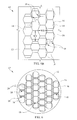
- lenses 16 can be integrally formed in a honeycomb pattern having hexagonally shaped lenses 16 . That is, by shifting every-other row of LED chips 14 , a honeycomb pattern of lenses 16 can be provided. One or more chips 14 can provided centrally below a center of each hexagonally shaped lens 16 .
- each lens 16 can be compressed in each direction, such that each lens 16 can comprise a maximum width W and W′ in each direction that can be less than a diameter of a sphere. In other aspects as illustrated in FIG.
- a distorted honeycomb pattern can be provided, where the honeycomb pattern can be stretched or compressed in one direction with respect to another direction, having different widths WX and WY. This can advantageously allow for a maximum packing density of LED chips 14 below lenses 16 with minimum intersection, thereby improving brightness.
- any size and/or shape of LED chips 14 can be provided.
- LED chips 14 can comprise a length and a width of approximately 1.35 mm.
- a ratio of row pitch to column pitch can be approximately 1.15 in FIG. 5A .
- the plurality of lenses 16 can be integrally formed and have some curvature such that top surfaces of lenses are non-flat or slightly curved.
- the lenses 16 can be compressed or stretched thereby forming a distorted honeycomb, where at least some of the hexagonal sides are different lengths.
- lenses 16 comprise distorted portions or areas 18 in which adjacent lenses 16 are distorted in portions or areas 18 between adjacent lenses 16 .
- lenses 16 can be distorted in a first direction.
- FIG. 6 illustrates a further aspect of a light emitter device, generally designated 70 .
- Emitter device 70 can comprise substrate 12 , two or more LED chips 14 and lenses 16 provided over one or more LED chips 14 .
- At least one LED chip 14 can be centrally or non-centrally disposed below each lens 16 .
- substrate 12 can comprise any non-rectangular or non-square shape, such as for example a circle.
- LED chips 14 can be arranged in an array comprising one or more rows over substrate 12 .
- one or more rows of the array can contain different quantities of LED chips 14 . That is, in some aspects, LED chips 14 can be arranged in a substantially circular array over a substantially circular substrate 12 . Any other suitable combinations of array shape and/or substrate shape can be provided. This can be useful to consumers by allowing different beam patterns, beam directions, and/or beam angles to be achieved.
- adjacent lenses 16 can be distorted as indicated by portions or areas 18 . That is, in some aspects, lenses 16 can be compressed and/or stretched, such as towards each other, in a direction. Notably, lenses 16 can comprise domes bounded by linear and curved surfaces, which can increase light extraction by allowing formation of integral lenses over tightly packed arrays of LED chips. For example some lenses can be bounded by distorted portions or areas 18 comprising linear surfaces or areas. Adjacent boundaries between distorted portions or areas 18 can comprise curved surfaces 24 or areas.
- Some lenses 16 can comprise a dome comprising different arc lengths, where one arc is approximately the width of at least one LED chip 14 , or slightly wider, and another arc is orthogonal to the one arc, and is longer than the one arc (see e.g., FIGS. 1C and 1D ). This can advantageously allow lenses to be provided over closely packed LED chips 14 , thereby maximizing light extraction and brightness from emitter device 70 .
- FIG. 7 is an exemplary embodiment of a molding block or tool, generally designated 80 .
- Tool 80 can be used for compression molding of lenses over LED chips, and can comprise one or more multiple molding cavities provided therein. Molding cavities can be configured to encapsulate multiple LED chips and/or provide molded lenses over multiple LED chips at a same time. As FIG. 6 illustrates, different types of molding cavities can be provided per tool 80 . For example, one or more flat molding cavities 82 and one or more integrated and distorted dome type cavities 84 can be provided on a same tool 80 . Notably, cavities 84 can provide integrally formed and substantially curved or domed lenses over multiple LED chips, where the lenses are distorted in one direction.
- lenses can be compressed or stretched along one direction, such that a width in that direction is different than a width in at least one other direction, such as an orthogonal direction. At least some of the lenses can be bounded by linear surfaces and curved surfaces as shown and described hereinabove.
- the integrally formed and/or distorted and non-flat lenses can contribute to improved brightness, while molding lenses over multiple LED chips at a same processing step can contribute to improved processing times and costs of providing emitter devices described herein.
- Light emitter devices and methods provided herein can comprise a luminous flux greater than approximately 2200 lumens (lm), greater than 2300 lm, greater than 2500 lm, or greater than 2600 lm. Light emitter devices and methods provided herein can be used in warm white, neutral white, or cool white lighting applications.
- Embodiments as disclosed herein may provide one or more of the following beneficial technical effects: reduced production costs; reduced processing time; improved manufacturability; improved brightness; and improved light extraction, among others.
Abstract
Description
Claims (32)
Priority Applications (1)
| Application Number | Priority Date | Filing Date | Title |
|---|---|---|---|
| US13/956,814 US9461024B2 (en) | 2013-08-01 | 2013-08-01 | Light emitter devices and methods for light emitting diode (LED) chips |
Applications Claiming Priority (1)
| Application Number | Priority Date | Filing Date | Title |
|---|---|---|---|
| US13/956,814 US9461024B2 (en) | 2013-08-01 | 2013-08-01 | Light emitter devices and methods for light emitting diode (LED) chips |
Publications (2)
| Publication Number | Publication Date |
|---|---|
| US20150034978A1 US20150034978A1 (en) | 2015-02-05 |
| US9461024B2 true US9461024B2 (en) | 2016-10-04 |
Family
ID=52426851
Family Applications (1)
| Application Number | Title | Priority Date | Filing Date |
|---|---|---|---|
| US13/956,814 Active US9461024B2 (en) | 2013-08-01 | 2013-08-01 | Light emitter devices and methods for light emitting diode (LED) chips |
Country Status (1)
| Country | Link |
|---|---|
| US (1) | US9461024B2 (en) |
Cited By (2)
| Publication number | Priority date | Publication date | Assignee | Title |
|---|---|---|---|---|
| US20170077172A1 (en) * | 2015-09-10 | 2017-03-16 | Panasonic Intellectual Property Management Co., Ltd. | Light-emitting device and illumination light source |
| US11681135B2 (en) * | 2017-05-12 | 2023-06-20 | Suzhou Institute Of Biomedical Engineering And Technology, Chinese Academy Of Sciences | Structured illumination microscopic imaging system |
Families Citing this family (7)
| Publication number | Priority date | Publication date | Assignee | Title |
|---|---|---|---|---|
| EP3259784A1 (en) * | 2015-02-19 | 2017-12-27 | Osram Sylvania Inc. | Led light source with diffuser |
| JP6643831B2 (en) * | 2015-08-31 | 2020-02-12 | シチズン電子株式会社 | Light emitting device |
| JP2017050344A (en) * | 2015-08-31 | 2017-03-09 | シチズン電子株式会社 | Light-emitting device |
| JP6610136B2 (en) * | 2015-09-30 | 2019-11-27 | 株式会社Gsユアサ | Lighting device |
| TWI685961B (en) * | 2016-06-17 | 2020-02-21 | 優顯科技股份有限公司 | Optoelectronic semiconductor device |
| US10180232B2 (en) * | 2016-08-31 | 2019-01-15 | Nichia Corporation | Optical member, light source device, and irradiation system |
| JP6913513B2 (en) * | 2017-05-25 | 2021-08-04 | オリンパス株式会社 | Lighting equipment for microscopes and microscopes |
Citations (211)
| Publication number | Priority date | Publication date | Assignee | Title |
|---|---|---|---|---|
| US4013916A (en) | 1975-10-03 | 1977-03-22 | Monsanto Company | Segmented light emitting diode deflector segment |
| US4118763A (en) | 1976-04-12 | 1978-10-03 | General Electric Company | Variable transmission prismatic refractors |
| US4143394A (en) | 1976-07-30 | 1979-03-06 | Licentia Patent-Verwaltungs-G.M.B.H. | Semiconductor luminescence device with housing |
| US4300185A (en) | 1979-12-07 | 1981-11-10 | C. W. Cole & Company, Inc. | Light fixture unit for open plan office |
| US4464707A (en) | 1982-03-17 | 1984-08-07 | Louis Forrest | Lighting fixture |
| US4472767A (en) | 1981-12-23 | 1984-09-18 | Mcgraw-Edison Company | Reflector assembly for indirect or semi-indirect lighting fixture |
| US4946547A (en) | 1989-10-13 | 1990-08-07 | Cree Research, Inc. | Method of preparing silicon carbide surfaces for crystal growth |
| EP0441622A1 (en) | 1990-02-07 | 1991-08-14 | Shin-Etsu Chemical Co., Ltd. | Epoxy resin compositions containing highly transparent silica-titania glass beads |
| US5040868A (en) | 1989-05-31 | 1991-08-20 | Siemens Aktiengesellschaft | Surface-mountable opto-component |
| US5200022A (en) | 1990-10-03 | 1993-04-06 | Cree Research, Inc. | Method of improving mechanically prepared substrate surfaces of alpha silicon carbide for deposition of beta silicon carbide thereon and resulting product |
| USRE34861E (en) | 1987-10-26 | 1995-02-14 | North Carolina State University | Sublimation of silicon carbide to produce large, device quality single crystals of silicon carbide |
| US5530628A (en) | 1993-04-05 | 1996-06-25 | Peerless Lighting Corporation | Task light |
| US5690415A (en) | 1995-11-29 | 1997-11-25 | Stylmark, Inc. | Display light |
| US5951150A (en) | 1997-09-11 | 1999-09-14 | Eaton Corporation | Display system |
| US6061160A (en) | 1996-05-31 | 2000-05-09 | Dowa Mining Co., Ltd. | Component device for optical communication |
| JP2000188358A (en) | 1998-12-22 | 2000-07-04 | Rohm Co Ltd | Semiconductor device |
| JP2000223752A (en) | 1999-01-29 | 2000-08-11 | Nichia Chem Ind Ltd | Optical semiconductor device and its forming method |
| JP2001301230A (en) | 2000-04-25 | 2001-10-30 | Sharp Corp | Exposing unit |
| US6350041B1 (en) | 1999-12-03 | 2002-02-26 | Cree Lighting Company | High output radial dispersing lamp using a solid state light source |
| US6376902B1 (en) | 1997-07-29 | 2002-04-23 | Osram Opto Semiconductors Gmbh & Co. Ohg | Optoelectronic structural element |
| US6435697B1 (en) | 2001-02-02 | 2002-08-20 | Joseph E. Simmons | Exterior lighting system |
| US20020123163A1 (en) | 2000-04-24 | 2002-09-05 | Takehiro Fujii | Edge-emitting light-emitting semiconductor device and method of manufacture thereof |
| US6457844B2 (en) | 2000-05-10 | 2002-10-01 | Regent Beleuchtungskoerper Ag | Light distributor for a lighting device and lighting device and use of a lighting device |
| US20020163302A1 (en) | 2001-04-09 | 2002-11-07 | Koichi Nitta | Light emitting device |
| US20020163001A1 (en) | 2001-05-04 | 2002-11-07 | Shaddock David Mulford | Surface mount light emitting device package and fabrication method |
| US20030008431A1 (en) | 2001-03-30 | 2003-01-09 | Sumitomo Electric Industries, Ltd. | Light emitting device |
| US6521915B2 (en) | 2000-03-14 | 2003-02-18 | Asahi Rubber Inc. | Light-emitting diode device |
| US6536924B2 (en) | 2001-02-28 | 2003-03-25 | Jji Lighting Group, Inc. | Modular lighting unit |
| CN1417868A (en) | 2001-10-29 | 2003-05-14 | 银河光电股份有限公司 | Multiple-chip package structure of LED chip |
| JP2003197974A (en) | 2001-12-24 | 2003-07-11 | Samsung Electro Mech Co Ltd | Light emitting diode package |
| US6667451B1 (en) | 2003-03-20 | 2003-12-23 | Eaton Corporation | Push button assembly |
| US6686676B2 (en) | 2001-04-30 | 2004-02-03 | General Electric Company | UV reflectors and UV-based light sources having reduced UV radiation leakage incorporating the same |
| US20040041222A1 (en) | 2002-09-04 | 2004-03-04 | Loh Ban P. | Power surface mount light emitting die package |
| US20040079957A1 (en) | 2002-09-04 | 2004-04-29 | Andrews Peter Scott | Power surface mount light emitting die package |
| US6739734B1 (en) | 2003-03-17 | 2004-05-25 | Ultimate Presentation Sytems, Inc. | LED retrofit method and kit for converting fluorescent luminaries |
| WO2004053933A2 (en) | 2002-12-06 | 2004-06-24 | Cree, Inc. | Composite leadframe led package and method of making the same |
| US20040130880A1 (en) | 2003-01-07 | 2004-07-08 | Samsung Electronics Co., Ltd. | Backlight unit |
| USD494550S1 (en) | 2003-08-26 | 2004-08-17 | Nichia Corporation | Light emitting diode |
| US20040217364A1 (en) | 2003-05-01 | 2004-11-04 | Cree Lighting Company, Inc. | Multiple component solid state white light |
| US20040218390A1 (en) | 2003-01-24 | 2004-11-04 | Digital Optics International Corporation | High-density illumination system |
| US20040227149A1 (en) | 2003-04-30 | 2004-11-18 | Cree, Inc. | High powered light emitter packages with compact optics |
| US20040240214A1 (en) | 2003-05-28 | 2004-12-02 | Hubbell Incorporated. | Light fixture having air ducts |
| US20050073244A1 (en) | 2003-10-01 | 2005-04-07 | Chou Der Jeou | Methods and apparatus for an LED light |
| US20050073840A1 (en) | 2003-10-01 | 2005-04-07 | Chou Der Jeou | Methods and apparatus for an LED light engine |
| EP1529807A2 (en) | 2003-10-16 | 2005-05-11 | Nitto Denko Corporation | Epoxy resin composition for encapsulating optical semiconductor element and optical semiconductor device using the same |
| US6900511B2 (en) | 2002-06-28 | 2005-05-31 | Osram Opto Semiconductors Gmbh | Optoelectronic component and method for producing it |
| US6914194B2 (en) | 2003-10-29 | 2005-07-05 | Ben Fan | Flexible LED cable light |
| US20050173708A1 (en) | 2004-02-06 | 2005-08-11 | Toyoda Gosei Co., Ltd. | Light emitting device and sealing material |
| US6940704B2 (en) | 2001-01-24 | 2005-09-06 | Gelcore, Llc | Semiconductor light emitting device |
| USD511329S1 (en) | 2003-07-09 | 2005-11-08 | Nichia Corporation | Light emitting diode |
| US7009343B2 (en) | 2004-03-11 | 2006-03-07 | Kevin Len Li Lim | System and method for producing white light using LEDs |
| US20060050505A1 (en) | 2002-05-28 | 2006-03-09 | Kenall Manufacturing Company | Selectively-extendable modular lighting fixture and method |
| US20060049477A1 (en) | 2002-11-29 | 2006-03-09 | Karlheinz Arndt | Optoelectronic component |
| US20060049421A1 (en) | 2004-09-09 | 2006-03-09 | Toyoda Gosei Co., Ltd. | Solid-state optical device |
| USD517027S1 (en) | 2003-12-05 | 2006-03-14 | Nichia Corporation | Light emitting diode |
| US20060060882A1 (en) | 2004-09-22 | 2006-03-23 | Sharp Kabushiki Kaisha | Optical semiconductor device, optical communication device, and electronic equipment |
| US20060097245A1 (en) | 2002-08-30 | 2006-05-11 | Aanegola Srinath K | Light emitting diode component |
| US20060097385A1 (en) | 2004-10-25 | 2006-05-11 | Negley Gerald H | Solid metal block semiconductor light emitting device mounting substrates and packages including cavities and heat sinks, and methods of packaging same |
| US20060102917A1 (en) | 2002-06-19 | 2006-05-18 | Toshihiko Oyama | Semiconductor light emitting device, method for producing the same and reflector for semiconductor light emitting device |
| US7048416B2 (en) | 2003-06-13 | 2006-05-23 | Finelite, Inc. | Free-cavity, double-diffusing indirect lighting luminaire |
| CN1776506A (en) | 2005-12-08 | 2006-05-24 | 友达光电股份有限公司 | Light-emitting assembly packaing structure, Backlight module applying it and liquid crystal display device thereof |
| WO2006059828A1 (en) | 2004-09-10 | 2006-06-08 | Seoul Semiconductor Co., Ltd. | Light emitting diode package having multiple molding resins |
| WO2006060141A2 (en) | 2004-11-16 | 2006-06-08 | Nanocrystal Lighting Corporation | Optically reliable nanoparticle based nanocomposite hri encapsulant and photonic waveguiding material |
| US20060124946A1 (en) | 2003-06-06 | 2006-06-15 | Sharp Kabushiki Kaisha | Optical transmitter |
| JP2006165029A (en) | 2004-12-02 | 2006-06-22 | Fujikura Ltd | Substrate for mounting light emitting element and light emitting element package |
| US7066626B2 (en) | 2003-04-09 | 2006-06-27 | Citizen Electronics Co., Ltd. | LED lamp |
| US7070303B2 (en) | 2003-12-31 | 2006-07-04 | Kassay Charles E | Fluorescent lighting fixtures with controlled uplight capability |
| US20060186431A1 (en) | 2005-02-18 | 2006-08-24 | Nichia Corporation | Light emitting device provided with lens for controlling light distribution characteristic |
| US7131747B1 (en) | 2003-12-29 | 2006-11-07 | Yates James P | Length adjustment device for illuminated fascia |
| US20060273337A1 (en) | 2005-06-01 | 2006-12-07 | Samsung Electro-Mechanics Co., Ltd | Side-emitting LED package and method of manufacturing the same |
| US20060278882A1 (en) | 2005-06-10 | 2006-12-14 | Cree, Inc. | Power lamp package |
| US20060278886A1 (en) | 2005-06-10 | 2006-12-14 | Sony Corporation | Light emitting diode, method of manufacturing light emitting diode, light emitting diode backlight, light emitting diode illuminating device, light emitting diode display, and electronic apparatus |
| US20060291185A1 (en) * | 2005-06-28 | 2006-12-28 | Sato Atsushi | Planar light source device and display using the same |
| US20070029569A1 (en) | 2005-08-04 | 2007-02-08 | Peter Andrews | Packages for semiconductor light emitting devices utilizing dispensed encapsulants and methods of packaging the same |
| US7213940B1 (en) | 2005-12-21 | 2007-05-08 | Led Lighting Fixtures, Inc. | Lighting device and lighting method |
| US7217023B2 (en) | 2002-08-01 | 2007-05-15 | Toyoda Gosei Co., Ltd. | Linear luminous body and linear luminous structure |
| US20070108462A1 (en) | 2004-08-17 | 2007-05-17 | Samsung Electro-Mechanics Co., Ltd. | Fabrication method of light emitting diode incorporating substrate surface treatment by laser and light emitting diode fabricated thereby |
| US7224000B2 (en) | 2002-08-30 | 2007-05-29 | Lumination, Llc | Light emitting diode component |
| US7228253B2 (en) | 2004-08-19 | 2007-06-05 | Pacific Telescope Corp. | Instrument mounting system with dual encoders |
| CN1977399A (en) | 2005-04-01 | 2007-06-06 | 松下电器产业株式会社 | LED component and method for manufacturing same |
| US20070158668A1 (en) | 2005-08-25 | 2007-07-12 | Cree, Inc. | Close loop electrophoretic deposition of semiconductor devices |
| US7253448B2 (en) | 1999-03-15 | 2007-08-07 | Gentex Corporation | Semiconductor radiation emitter package |
| US20070201225A1 (en) | 2006-02-27 | 2007-08-30 | Illumination Management Systems | LED device for wide beam generation |
| US7265365B2 (en) | 2005-05-24 | 2007-09-04 | Dubois Equipment Company, Inc. | Apparatus for curing a coating on a three-dimensional object |
| US7282785B2 (en) | 2004-01-05 | 2007-10-16 | Stanley Electric Co., Ltd. | Surface mount type semiconductor device and lead frame structure thereof |
| JP2007287981A (en) | 2006-04-18 | 2007-11-01 | Konica Minolta Opto Inc | Light emitting device |
| US20070252250A1 (en) | 2006-04-26 | 2007-11-01 | Cotco Holdings Limited, A Hong Kong Corporation | Apparatus and method for use in mounting electronic elements |
| US20070262339A1 (en) | 2006-04-24 | 2007-11-15 | Cree, Inc. | Side-View Surface Mount White LED |
| JP2007299905A (en) | 2006-04-28 | 2007-11-15 | Nichia Chem Ind Ltd | Semiconductor device |
| US7317181B2 (en) | 2001-12-07 | 2008-01-08 | Hitachi Cable, Ltd. | Light-emitting unit and method for producing same as well as lead frame used for producing light-emitting unit |
| WO2008003289A2 (en) | 2006-07-06 | 2008-01-10 | Osram Gesellschaft mit beschränkter Haftung | Illuminating system of flexible shape |
| KR100809658B1 (en) | 2007-06-27 | 2008-03-05 | 김재을 | Lens for led and led display device using thereof it |
| US7344952B2 (en) | 2005-10-28 | 2008-03-18 | Philips Lumileds Lighting Company, Llc | Laminating encapsulant film containing phosphor over LEDs |
| US20080128723A1 (en) | 2006-12-04 | 2008-06-05 | Siew It Pang | Low Thermal Resistance High Power LED |
| US7387410B2 (en) | 2004-09-07 | 2008-06-17 | C.E.I.T. Corp. | Luminaire assembly and method |
| USD572210S1 (en) | 2006-11-01 | 2008-07-01 | Lg Innotek Co., Ltd. | Light-emitting diode (LED) |
| US20080173884A1 (en) | 2007-01-22 | 2008-07-24 | Cree, Inc. | Wafer level phosphor coating method and devices fabricated utilizing method |
| US20080179611A1 (en) | 2007-01-22 | 2008-07-31 | Cree, Inc. | Wafer level phosphor coating method and devices fabricated utilizing method |
| EP1953834A1 (en) | 2005-11-21 | 2008-08-06 | Matsushita Electric Works, Ltd. | Light-emitting device |
| USD576574S1 (en) | 2007-07-17 | 2008-09-09 | Rohm Co., Ltd. | Light emitting diode module |
| US20080258130A1 (en) | 2007-04-23 | 2008-10-23 | Bergmann Michael J | Beveled LED Chip with Transparent Substrate |
| US20080314944A1 (en) | 2007-06-21 | 2008-12-25 | Cheng-Yu Tsai | Assembly for fixing and connecting light bar lamp |
| US20090040782A1 (en) | 2007-08-08 | 2009-02-12 | Ledtech Electronics Corp. | Led lighting device |
| US20090046457A1 (en) | 2007-08-13 | 2009-02-19 | Everhart Robert L | Solid-state lighting fixtures |
| US20090050907A1 (en) | 2005-01-10 | 2009-02-26 | Cree, Inc. | Solid state lighting component |
| US20090057699A1 (en) | 2007-09-04 | 2009-03-05 | Philips Lumileds Lighting Company, Llc | LED with Particles in Encapsulant for Increased Light Extraction and Non-Yellow Off-State Color |
| EP2042528A1 (en) | 2007-09-25 | 2009-04-01 | Sony Chemical & Information Device Corporation | Curable resin composition |
| US20090091045A1 (en) | 2006-04-26 | 2009-04-09 | Sekisui Chemical Co., Ltd | Themosetting Composition for Optical Semiconductor, Die Bond Material for Optical Semiconductor Device, Underfill Material for Optical Semiconductor Device, Sealing Agent for Optical Semiconductor Device, and Optical Semiconductor Device |
| US20090108281A1 (en) | 2007-10-31 | 2009-04-30 | Cree, Inc. | Light emitting diode package and method for fabricating same |
| USD591697S1 (en) | 2006-08-09 | 2009-05-05 | Cree, Inc. | Lamp package |
| US7540627B2 (en) | 2006-05-08 | 2009-06-02 | Innovative Lighting, Inc. | Channel light system with pivotable connector |
| US20090161356A1 (en) | 2007-05-30 | 2009-06-25 | Cree Led Lighting Solutions, Inc. | Lighting device and method of lighting |
| US20090184333A1 (en) | 2008-01-17 | 2009-07-23 | Foxsemicon Integrated Technology, Inc. | Light emitting diode device |
| US20090207602A1 (en) | 2005-09-06 | 2009-08-20 | Reed Mark C | Linear lighting system |
| US20090212304A1 (en) | 2008-02-22 | 2009-08-27 | Bily Wang | Led chip package structure with multifunctional integrated chips and a method for making the same |
| US20090224265A1 (en) | 2008-03-05 | 2009-09-10 | Bily Wang | LED chip package structure with a high-efficiency heat-dissipating substrate and method for making the same |
| US20090262515A1 (en) | 2004-05-06 | 2009-10-22 | Seoul Opto-Device Co., Ltd. | Light emitting device |
| EP2113949A2 (en) | 2008-05-02 | 2009-11-04 | Cree, Inc. | Encapsulation for phosphor-converted white light emitting diode |
| US20090272995A1 (en) | 2005-09-30 | 2009-11-05 | Nitto Denko Corporation | Resin composition for optical semiconductor element encapsulation, and optical semiconductor device produced by using the same |
| US7614759B2 (en) | 2005-12-22 | 2009-11-10 | Cree Led Lighting Solutions, Inc. | Lighting device |
| US20090283781A1 (en) | 2008-05-16 | 2009-11-19 | Cree Hong Kong Limited | Mini V SMD |
| US20090290345A1 (en) | 2008-05-20 | 2009-11-26 | Apl Ip Holding Llc | Enclosures for led circuit boards |
| US20090290348A1 (en) | 2006-04-16 | 2009-11-26 | Peter Van Laanen | Thermal Management Of LED-Based Lighting Systems |
| US20090296381A1 (en) | 2008-06-01 | 2009-12-03 | Jack Dubord | Adjustable modular lighting system and method of using same |
| US7628506B2 (en) | 2005-10-03 | 2009-12-08 | Orion Energy Systems, Inc. | Modular light fixture with power pack and radiative, conductive, and convective cooling |
| US20100002426A1 (en) | 2008-06-25 | 2010-01-07 | Hubbell Incorporated | Multi-directional lighting fixture |
| US20100002307A1 (en) * | 2008-07-01 | 2010-01-07 | Oki Data Corporation | Lens array, led head, exposure device, image forming apparatus and reading apparatus |
| US7654703B2 (en) | 2004-01-28 | 2010-02-02 | Koninklijke Philips Electronics, N.V. | Directly viewable luminaire |
| EP2149920A1 (en) | 2007-05-17 | 2010-02-03 | Showa Denko K.K. | Semiconductor light-emitting device |
| USD615504S1 (en) | 2007-10-31 | 2010-05-11 | Cree, Inc. | Emitter package |
| US7722220B2 (en) | 2006-05-05 | 2010-05-25 | Cree Led Lighting Solutions, Inc. | Lighting device |
| US20100142205A1 (en) | 2008-12-08 | 2010-06-10 | Avx Corporation | Two part surface mount led strip connector and led assembly |
| EP2196501A1 (en) | 2008-12-15 | 2010-06-16 | Nichia Corporation | Thermoseting epoxy resin composition and semiconductor device |
| US20100155763A1 (en) | 2008-01-15 | 2010-06-24 | Cree, Inc. | Systems and methods for application of optical materials to optical elements |
| US20100171404A1 (en) | 2009-01-07 | 2010-07-08 | Fu Zhun Precision Industry (Shen Zhen) Co., Ltd. | Led lamp |
| US7758207B1 (en) | 2009-03-17 | 2010-07-20 | Fu Zhun Precision Industry (Shen Zhen) Co., Ltd. | Lightweight LED lamp |
| US7762692B2 (en) | 2007-08-14 | 2010-07-27 | Foxsemicon Integrated Technology, Inc. | Surface mount light emitting diode assembly and backlight module using the same |
| US20100214785A1 (en) | 2009-02-23 | 2010-08-26 | Chen Hui Yu | Waterproof lighting fixture |
| US20100214770A1 (en) | 2009-02-25 | 2010-08-26 | Anderson Kenneth E | Combination LED fixture and raceway |
| US20100220469A1 (en) | 2008-05-23 | 2010-09-02 | Altair Engineering, Inc. | D-shaped cross section l.e.d. based light |
| US7791061B2 (en) | 2004-05-18 | 2010-09-07 | Cree, Inc. | External extraction light emitting diode based upon crystallographic faceted surfaces |
| US20100252851A1 (en) | 2007-10-31 | 2010-10-07 | Cree, Inc. | Led package with increased feature sizes |
| US20100259927A1 (en) | 2009-04-09 | 2010-10-14 | Chien Hsiao-Lou | Led lamp structure |
| US20100295070A1 (en) * | 2009-05-20 | 2010-11-25 | Intematix Corporation | Light emitting device |
| US20100328945A1 (en) | 2009-06-30 | 2010-12-30 | Fu Zhun Precision Industry (Shen Zhen) Co., Ltd. | Led lamp |
| US20110001151A1 (en) | 2009-07-06 | 2011-01-06 | Cree, Inc. | Led packages with scattering particle regions |
| US20110007514A1 (en) | 2008-05-09 | 2011-01-13 | Sloanled, Inc. | Low profile extrusion |
| US20110006688A1 (en) | 2008-02-26 | 2011-01-13 | Shim Hyun-Seop | Led lamp device |
| USD631020S1 (en) | 2010-04-29 | 2011-01-18 | Edison Opto Corporation | LED package |
| US20110013400A1 (en) | 2009-07-16 | 2011-01-20 | Japan Aviation Electronics Industry, Limited | Socket, circuit board assembly, and apparatus having the same |
| US20110028006A1 (en) | 2008-03-20 | 2011-02-03 | Ashok Deepak Shah | Conductive Magnetic Coupling System |
| US20110031527A1 (en) | 2008-01-09 | 2011-02-10 | Hitachi Chemical Company, Ltd. | Thermosetting resin composition, epoxy resin molding material, and polyvalent carboxylic acid condensate |
| USD633631S1 (en) | 2007-12-14 | 2011-03-01 | Cree Hong Kong Limited | Light source of light emitting diode |
| USD634863S1 (en) | 2008-01-10 | 2011-03-22 | Cree Hong Kong Limited | Light source of light emitting diode |
| US20110090682A1 (en) | 2009-10-15 | 2011-04-21 | Fu Zhun Precision Industry (Shen Zhen) Co., Ltd. | Led tube |
| US20110103043A1 (en) | 2008-06-27 | 2011-05-05 | Optoworld Co., Ltd. | Device for Supporting Light Emitting Module |
| WO2011061650A1 (en) | 2009-11-23 | 2011-05-26 | Koninklijke Philips Electronics N.V. | Wavelength converted semiconductor light emitting diode |
| US20110140289A1 (en) | 2009-12-15 | 2011-06-16 | Toshio Shiobara | Resin composition for encapsulating optical semiconductor element and optical semiconductor device |
| US20110149604A1 (en) | 2006-09-01 | 2011-06-23 | Cree, Inc. | Encapsulant profile for light emitting diodes |
| US20110156061A1 (en) | 2009-12-30 | 2011-06-30 | Harvatek Corporation | Light emission module with high-efficiency light emission and high-efficiency heat dissipation and applications thereof |
| US20110163683A1 (en) | 2011-02-22 | 2011-07-07 | Quarkstar, Llc | Solid State Lamp Using Light Emitting Strips |
| US20110211330A1 (en) | 2010-03-01 | 2011-09-01 | Wen Wen Wang | Lighting apparatus |
| US20110215345A1 (en) | 2010-03-03 | 2011-09-08 | Cree, Inc. | Solid state lamp with thermal spreading elements and light directing optics |
| US20110221330A1 (en) | 2010-03-09 | 2011-09-15 | Cree, Inc. | High cri lighting device with added long-wavelength blue color |
| US20110220920A1 (en) | 2010-03-09 | 2011-09-15 | Brian Thomas Collins | Methods of forming warm white light emitting devices having high color rendering index values and related light emitting devices |
| US20110228514A1 (en) | 2010-03-03 | 2011-09-22 | Cree, Inc. | Enhanced color rendering index emitter through phosphor separation |
| US8044418B2 (en) | 2006-07-13 | 2011-10-25 | Cree, Inc. | Leadframe-based packages for solid state light emitting devices |
| US8047673B2 (en) | 2007-04-10 | 2011-11-01 | Philips Electronics Ltd | Light control device exhibiting batwing luminous intensity distributions in upper and lower hemispheres |
| US8058088B2 (en) | 2008-01-15 | 2011-11-15 | Cree, Inc. | Phosphor coating systems and methods for light emitting structures and packaged light emitting diodes including phosphor coating |
| US20110286208A1 (en) | 2010-05-24 | 2011-11-24 | Yu-Wen Chen | Light source assembly mechanism for led lamps |
| US20110285314A1 (en) | 2010-04-27 | 2011-11-24 | Cooper Technologies Company | Linkable Linear Light Emitting Diode System |
| US20110286207A1 (en) | 2010-04-28 | 2011-11-24 | Cooper Technologies Company | Linear LED Light Module |
| US20110291131A1 (en) * | 2009-02-19 | 2011-12-01 | Shin Ito | Light emitting device, planar light source, and display device |
| USD650342S1 (en) | 2010-06-22 | 2011-12-13 | Panasonic Corporation | Light emitting diode |
| US20110310604A1 (en) | 2010-06-17 | 2011-12-22 | Rohm Co., Ltd. | Led lamp, lamp case, led module and led lighting apparatus |
| US20110316022A1 (en) * | 2010-06-28 | 2011-12-29 | Hussell Christopher P | Led package with efficient, isolated thermal path |
| US20110316006A1 (en) | 2010-02-11 | 2011-12-29 | Tao Xu | Surface-Textured Encapsulations for use with Light Emitting Diodes |
| US20120051041A1 (en) | 2010-08-31 | 2012-03-01 | Cree, Inc. | Troffer-Style Fixture |
| US20120062821A1 (en) | 2009-03-10 | 2012-03-15 | Toshiba Materials Co., Ltd. | White led, backlight using same, and liquid crystal display device conforming to ebu standard |
| US20120061703A1 (en) | 2010-06-01 | 2012-03-15 | Kabushiki Kaisha Toshiba | Light emitting device and manufacturing method of light emitting device |
| US20120068198A1 (en) | 2010-09-20 | 2012-03-22 | Cree, Inc. | High density multi-chip led devices |
| US20120075857A1 (en) | 2009-02-24 | 2012-03-29 | Koninklijke Philips Electronics N.V. | Directable magnetic mount for light emitter, a light source, a base and an illumination system |
| US20120081883A1 (en) | 2010-10-04 | 2012-04-05 | Yu-Chin Wang | Led lamp for aquarium |
| US20120098424A1 (en) | 2010-10-21 | 2012-04-26 | General Electric Company | Lighting system with thermal management system having point contact synthetic jets |
| US20120120666A1 (en) | 2009-05-13 | 2012-05-17 | Hella Kgaa Hueck & Co. | Street lighting device |
| US8206004B2 (en) | 2009-07-07 | 2012-06-26 | American Fluorescent Corporation | Distributed lighting apparatus |
| US20120169234A1 (en) | 2009-12-31 | 2012-07-05 | Shew Larry N | Light assembly |
| US20120193651A1 (en) | 2010-11-22 | 2012-08-02 | Edmond John A | Light emitting devices, systems, and methods |
| US20120218757A1 (en) | 2009-11-05 | 2012-08-30 | Amoluxe Co., Ltd. | Lighting apparatus using light emitting diodes |
| WO2012120434A1 (en) | 2011-03-07 | 2012-09-13 | Koninklijke Philips Electronics N.V. | A light emitting module, a lamp, a luminaire and a display device |
| US20120235190A1 (en) | 2011-03-18 | 2012-09-20 | Cree, Inc. | Encapsulant with index matched thixotropic agent |
| US20120250302A1 (en) | 2011-03-07 | 2012-10-04 | Greendot Technologies, Llc | Vapor-tight lighting fixture |
| US8313212B1 (en) | 2009-05-29 | 2012-11-20 | Usai, Llc | Modular lighting system and method |
| US8317369B2 (en) | 2009-04-02 | 2012-11-27 | Abl Ip Holding Llc | Light fixture having selectively positionable housing |
| US20120300456A1 (en) * | 2011-05-26 | 2012-11-29 | Phillips Iii William E | Reflectors optimized for led lighting fixture |
| US8342714B1 (en) | 2009-05-06 | 2013-01-01 | Stray Light Optical Technologies | Mobile lighting apparatus |
| US8376578B2 (en) | 2009-06-12 | 2013-02-19 | Lg Innotek Co., Ltd. | Lighting device |
| US20130050998A1 (en) | 2011-08-25 | 2013-02-28 | Gt Biomescilt Light Limited | Light emitting diode lamp with light diffusing structure |
| US20130094225A1 (en) | 2011-10-17 | 2013-04-18 | Ecosense Lighting Inc. | Linear led light housing |
| US8459824B1 (en) | 2009-12-01 | 2013-06-11 | Ashkan Esmailzadeh | Lighting fixture |
| US8523383B1 (en) | 2010-02-19 | 2013-09-03 | Cooper Technologies Company | Retrofitting recessed lighting fixtures |
| US20130271979A1 (en) | 2012-04-17 | 2013-10-17 | Dennis Pearson | Scalable LED Sconce Light |
| US20130279180A1 (en) | 2012-04-23 | 2013-10-24 | Dennis Pearson | Commercial Lighting Integrated Platform |
| US20130329425A1 (en) | 2012-06-11 | 2013-12-12 | Cree, Inc. | Led package with encapsulant having planar surfaces |
| US8714770B2 (en) | 2008-08-01 | 2014-05-06 | Nichia Corporation | Lighting device |
| US8729586B2 (en) | 2011-10-31 | 2014-05-20 | Lite-On Electronics (Guangzhou) Limited | Light-emitting diode device |
| US8835957B2 (en) | 2011-03-24 | 2014-09-16 | Nichia Corporation | Light emitting device and method for manufacturing the same |
| US20140265809A1 (en) | 2013-03-15 | 2014-09-18 | Cree, Inc. | Connector devices, systems, and related methods for light emitter components |
| US8888316B2 (en) | 2011-12-20 | 2014-11-18 | Innovative Lighting, Inc. | Lenticular LED light source replacement for fluorescent in troffer |
| US9028120B2 (en) | 2011-08-08 | 2015-05-12 | Quarkstar Llc | Illumination devices including multiple light emitting elements |
| US9057493B2 (en) | 2010-03-26 | 2015-06-16 | Ilumisys, Inc. | LED light tube with dual sided light distribution |
-
2013
- 2013-08-01 US US13/956,814 patent/US9461024B2/en active Active
Patent Citations (236)
| Publication number | Priority date | Publication date | Assignee | Title |
|---|---|---|---|---|
| US4013916A (en) | 1975-10-03 | 1977-03-22 | Monsanto Company | Segmented light emitting diode deflector segment |
| US4118763A (en) | 1976-04-12 | 1978-10-03 | General Electric Company | Variable transmission prismatic refractors |
| US4143394A (en) | 1976-07-30 | 1979-03-06 | Licentia Patent-Verwaltungs-G.M.B.H. | Semiconductor luminescence device with housing |
| US4300185A (en) | 1979-12-07 | 1981-11-10 | C. W. Cole & Company, Inc. | Light fixture unit for open plan office |
| US4472767A (en) | 1981-12-23 | 1984-09-18 | Mcgraw-Edison Company | Reflector assembly for indirect or semi-indirect lighting fixture |
| US4464707A (en) | 1982-03-17 | 1984-08-07 | Louis Forrest | Lighting fixture |
| USRE34861E (en) | 1987-10-26 | 1995-02-14 | North Carolina State University | Sublimation of silicon carbide to produce large, device quality single crystals of silicon carbide |
| EP1187227A2 (en) | 1989-05-31 | 2002-03-13 | Osram Opto Semiconductors GmbH & Co. OHG | Surface-mountable optical element and method of fabrication |
| US5040868A (en) | 1989-05-31 | 1991-08-20 | Siemens Aktiengesellschaft | Surface-mountable opto-component |
| US4946547A (en) | 1989-10-13 | 1990-08-07 | Cree Research, Inc. | Method of preparing silicon carbide surfaces for crystal growth |
| EP0441622A1 (en) | 1990-02-07 | 1991-08-14 | Shin-Etsu Chemical Co., Ltd. | Epoxy resin compositions containing highly transparent silica-titania glass beads |
| US5200022A (en) | 1990-10-03 | 1993-04-06 | Cree Research, Inc. | Method of improving mechanically prepared substrate surfaces of alpha silicon carbide for deposition of beta silicon carbide thereon and resulting product |
| US5530628A (en) | 1993-04-05 | 1996-06-25 | Peerless Lighting Corporation | Task light |
| US5690415A (en) | 1995-11-29 | 1997-11-25 | Stylmark, Inc. | Display light |
| US6061160A (en) | 1996-05-31 | 2000-05-09 | Dowa Mining Co., Ltd. | Component device for optical communication |
| US6759733B2 (en) | 1997-07-29 | 2004-07-06 | Osram Opto Semiconductors Gmbh | Optoelectric surface-mountable structural element |
| US6376902B1 (en) | 1997-07-29 | 2002-04-23 | Osram Opto Semiconductors Gmbh & Co. Ohg | Optoelectronic structural element |
| US20040238930A1 (en) | 1997-07-29 | 2004-12-02 | Osram Opto Semiconductors Gmbh | Surface-mountable light-emitting diode structural element |
| US7183632B2 (en) | 1997-07-29 | 2007-02-27 | Osram Gmbh | Surface-mountable light-emitting diode structural element |
| US7102215B2 (en) | 1997-07-29 | 2006-09-05 | Osram Gmbh | Surface-mountable light-emitting diode structural element |
| US5951150A (en) | 1997-09-11 | 1999-09-14 | Eaton Corporation | Display system |
| JP2000188358A (en) | 1998-12-22 | 2000-07-04 | Rohm Co Ltd | Semiconductor device |
| JP2000223752A (en) | 1999-01-29 | 2000-08-11 | Nichia Chem Ind Ltd | Optical semiconductor device and its forming method |
| US7253448B2 (en) | 1999-03-15 | 2007-08-07 | Gentex Corporation | Semiconductor radiation emitter package |
| US6350041B1 (en) | 1999-12-03 | 2002-02-26 | Cree Lighting Company | High output radial dispersing lamp using a solid state light source |
| US6521915B2 (en) | 2000-03-14 | 2003-02-18 | Asahi Rubber Inc. | Light-emitting diode device |
| US20020123163A1 (en) | 2000-04-24 | 2002-09-05 | Takehiro Fujii | Edge-emitting light-emitting semiconductor device and method of manufacture thereof |
| JP2001301230A (en) | 2000-04-25 | 2001-10-30 | Sharp Corp | Exposing unit |
| US6457844B2 (en) | 2000-05-10 | 2002-10-01 | Regent Beleuchtungskoerper Ag | Light distributor for a lighting device and lighting device and use of a lighting device |
| US6940704B2 (en) | 2001-01-24 | 2005-09-06 | Gelcore, Llc | Semiconductor light emitting device |
| US6435697B1 (en) | 2001-02-02 | 2002-08-20 | Joseph E. Simmons | Exterior lighting system |
| US6536924B2 (en) | 2001-02-28 | 2003-03-25 | Jji Lighting Group, Inc. | Modular lighting unit |
| US20030008431A1 (en) | 2001-03-30 | 2003-01-09 | Sumitomo Electric Industries, Ltd. | Light emitting device |
| CN1380703A (en) | 2001-04-09 | 2002-11-20 | 株式会社东芝 | Luminescent device |
| US20020163302A1 (en) | 2001-04-09 | 2002-11-07 | Koichi Nitta | Light emitting device |
| US20070085107A1 (en) | 2001-04-09 | 2007-04-19 | Kabushiki Kaisha Toshiba | Light Emitting Device |
| US6686676B2 (en) | 2001-04-30 | 2004-02-03 | General Electric Company | UV reflectors and UV-based light sources having reduced UV radiation leakage incorporating the same |
| US20020163001A1 (en) | 2001-05-04 | 2002-11-07 | Shaddock David Mulford | Surface mount light emitting device package and fabrication method |
| CN1417868A (en) | 2001-10-29 | 2003-05-14 | 银河光电股份有限公司 | Multiple-chip package structure of LED chip |
| US7317181B2 (en) | 2001-12-07 | 2008-01-08 | Hitachi Cable, Ltd. | Light-emitting unit and method for producing same as well as lead frame used for producing light-emitting unit |
| JP2003197974A (en) | 2001-12-24 | 2003-07-11 | Samsung Electro Mech Co Ltd | Light emitting diode package |
| US6707069B2 (en) | 2001-12-24 | 2004-03-16 | Samsung Electro-Mechanics Co., Ltd | Light emission diode package |
| US20060050505A1 (en) | 2002-05-28 | 2006-03-09 | Kenall Manufacturing Company | Selectively-extendable modular lighting fixture and method |
| US20060102917A1 (en) | 2002-06-19 | 2006-05-18 | Toshihiko Oyama | Semiconductor light emitting device, method for producing the same and reflector for semiconductor light emitting device |
| US7514279B2 (en) | 2002-06-28 | 2009-04-07 | Osram Opto Semiconductors Gmbh | Optoelectronic component and method for producing it |
| US6900511B2 (en) | 2002-06-28 | 2005-05-31 | Osram Opto Semiconductors Gmbh | Optoelectronic component and method for producing it |
| US7217023B2 (en) | 2002-08-01 | 2007-05-15 | Toyoda Gosei Co., Ltd. | Linear luminous body and linear luminous structure |
| US20060097245A1 (en) | 2002-08-30 | 2006-05-11 | Aanegola Srinath K | Light emitting diode component |
| US7224000B2 (en) | 2002-08-30 | 2007-05-29 | Lumination, Llc | Light emitting diode component |
| US20040041222A1 (en) | 2002-09-04 | 2004-03-04 | Loh Ban P. | Power surface mount light emitting die package |
| US20040079957A1 (en) | 2002-09-04 | 2004-04-29 | Andrews Peter Scott | Power surface mount light emitting die package |
| US20120235199A1 (en) | 2002-09-04 | 2012-09-20 | Peter Scott Andrews | Power surface mount light emitting die package |
| US7271425B2 (en) | 2002-11-29 | 2007-09-18 | Osram Opto Semiconductors Gmbh | Optoelectronic component |
| US20060049477A1 (en) | 2002-11-29 | 2006-03-09 | Karlheinz Arndt | Optoelectronic component |
| US20040126913A1 (en) | 2002-12-06 | 2004-07-01 | Loh Ban P. | Composite leadframe LED package and method of making the same |
| WO2004053933A2 (en) | 2002-12-06 | 2004-06-24 | Cree, Inc. | Composite leadframe led package and method of making the same |
| US20040130880A1 (en) | 2003-01-07 | 2004-07-08 | Samsung Electronics Co., Ltd. | Backlight unit |
| US20040218390A1 (en) | 2003-01-24 | 2004-11-04 | Digital Optics International Corporation | High-density illumination system |
| US6739734B1 (en) | 2003-03-17 | 2004-05-25 | Ultimate Presentation Sytems, Inc. | LED retrofit method and kit for converting fluorescent luminaries |
| US6667451B1 (en) | 2003-03-20 | 2003-12-23 | Eaton Corporation | Push button assembly |
| US7066626B2 (en) | 2003-04-09 | 2006-06-27 | Citizen Electronics Co., Ltd. | LED lamp |
| US20040227149A1 (en) | 2003-04-30 | 2004-11-18 | Cree, Inc. | High powered light emitter packages with compact optics |
| US20040217364A1 (en) | 2003-05-01 | 2004-11-04 | Cree Lighting Company, Inc. | Multiple component solid state white light |
| US20040240214A1 (en) | 2003-05-28 | 2004-12-02 | Hubbell Incorporated. | Light fixture having air ducts |
| CN1802756A (en) | 2003-06-06 | 2006-07-12 | 夏普株式会社 | Optical transmitter |
| US7281860B2 (en) | 2003-06-06 | 2007-10-16 | Sharp Kabushiki Kaisha | Optical transmitter |
| US20060124946A1 (en) | 2003-06-06 | 2006-06-15 | Sharp Kabushiki Kaisha | Optical transmitter |
| US7048416B2 (en) | 2003-06-13 | 2006-05-23 | Finelite, Inc. | Free-cavity, double-diffusing indirect lighting luminaire |
| USD511329S1 (en) | 2003-07-09 | 2005-11-08 | Nichia Corporation | Light emitting diode |
| USD511330S1 (en) | 2003-07-09 | 2005-11-08 | Nichia Corporation | Light emitting diode |
| USD494550S1 (en) | 2003-08-26 | 2004-08-17 | Nichia Corporation | Light emitting diode |
| US20050073840A1 (en) | 2003-10-01 | 2005-04-07 | Chou Der Jeou | Methods and apparatus for an LED light engine |
| US20050073244A1 (en) | 2003-10-01 | 2005-04-07 | Chou Der Jeou | Methods and apparatus for an LED light |
| EP1529807A2 (en) | 2003-10-16 | 2005-05-11 | Nitto Denko Corporation | Epoxy resin composition for encapsulating optical semiconductor element and optical semiconductor device using the same |
| US6914194B2 (en) | 2003-10-29 | 2005-07-05 | Ben Fan | Flexible LED cable light |
| USD517027S1 (en) | 2003-12-05 | 2006-03-14 | Nichia Corporation | Light emitting diode |
| US7131747B1 (en) | 2003-12-29 | 2006-11-07 | Yates James P | Length adjustment device for illuminated fascia |
| US7070303B2 (en) | 2003-12-31 | 2006-07-04 | Kassay Charles E | Fluorescent lighting fixtures with controlled uplight capability |
| US7282785B2 (en) | 2004-01-05 | 2007-10-16 | Stanley Electric Co., Ltd. | Surface mount type semiconductor device and lead frame structure thereof |
| US7654703B2 (en) | 2004-01-28 | 2010-02-02 | Koninklijke Philips Electronics, N.V. | Directly viewable luminaire |
| US20050173708A1 (en) | 2004-02-06 | 2005-08-11 | Toyoda Gosei Co., Ltd. | Light emitting device and sealing material |
| US7009343B2 (en) | 2004-03-11 | 2006-03-07 | Kevin Len Li Lim | System and method for producing white light using LEDs |
| US20090262515A1 (en) | 2004-05-06 | 2009-10-22 | Seoul Opto-Device Co., Ltd. | Light emitting device |
| US7791061B2 (en) | 2004-05-18 | 2010-09-07 | Cree, Inc. | External extraction light emitting diode based upon crystallographic faceted surfaces |
| US20070108462A1 (en) | 2004-08-17 | 2007-05-17 | Samsung Electro-Mechanics Co., Ltd. | Fabrication method of light emitting diode incorporating substrate surface treatment by laser and light emitting diode fabricated thereby |
| US7228253B2 (en) | 2004-08-19 | 2007-06-05 | Pacific Telescope Corp. | Instrument mounting system with dual encoders |
| US7387410B2 (en) | 2004-09-07 | 2008-06-17 | C.E.I.T. Corp. | Luminaire assembly and method |
| US20060049421A1 (en) | 2004-09-09 | 2006-03-09 | Toyoda Gosei Co., Ltd. | Solid-state optical device |
| WO2006059828A1 (en) | 2004-09-10 | 2006-06-08 | Seoul Semiconductor Co., Ltd. | Light emitting diode package having multiple molding resins |
| US20060060882A1 (en) | 2004-09-22 | 2006-03-23 | Sharp Kabushiki Kaisha | Optical semiconductor device, optical communication device, and electronic equipment |
| US20060097385A1 (en) | 2004-10-25 | 2006-05-11 | Negley Gerald H | Solid metal block semiconductor light emitting device mounting substrates and packages including cavities and heat sinks, and methods of packaging same |
| WO2006060141A2 (en) | 2004-11-16 | 2006-06-08 | Nanocrystal Lighting Corporation | Optically reliable nanoparticle based nanocomposite hri encapsulant and photonic waveguiding material |
| JP2006165029A (en) | 2004-12-02 | 2006-06-22 | Fujikura Ltd | Substrate for mounting light emitting element and light emitting element package |
| US20090050907A1 (en) | 2005-01-10 | 2009-02-26 | Cree, Inc. | Solid state lighting component |
| US20060186431A1 (en) | 2005-02-18 | 2006-08-24 | Nichia Corporation | Light emitting device provided with lens for controlling light distribution characteristic |
| CN1977399A (en) | 2005-04-01 | 2007-06-06 | 松下电器产业株式会社 | LED component and method for manufacturing same |
| US7265365B2 (en) | 2005-05-24 | 2007-09-04 | Dubois Equipment Company, Inc. | Apparatus for curing a coating on a three-dimensional object |
| US20060273337A1 (en) | 2005-06-01 | 2006-12-07 | Samsung Electro-Mechanics Co., Ltd | Side-emitting LED package and method of manufacturing the same |
| US20060278886A1 (en) | 2005-06-10 | 2006-12-14 | Sony Corporation | Light emitting diode, method of manufacturing light emitting diode, light emitting diode backlight, light emitting diode illuminating device, light emitting diode display, and electronic apparatus |
| US20060278882A1 (en) | 2005-06-10 | 2006-12-14 | Cree, Inc. | Power lamp package |
| US20060291185A1 (en) * | 2005-06-28 | 2006-12-28 | Sato Atsushi | Planar light source device and display using the same |
| US20070029569A1 (en) | 2005-08-04 | 2007-02-08 | Peter Andrews | Packages for semiconductor light emitting devices utilizing dispensed encapsulants and methods of packaging the same |
| US20070158668A1 (en) | 2005-08-25 | 2007-07-12 | Cree, Inc. | Close loop electrophoretic deposition of semiconductor devices |
| US20090207602A1 (en) | 2005-09-06 | 2009-08-20 | Reed Mark C | Linear lighting system |
| US20090272995A1 (en) | 2005-09-30 | 2009-11-05 | Nitto Denko Corporation | Resin composition for optical semiconductor element encapsulation, and optical semiconductor device produced by using the same |
| US7628506B2 (en) | 2005-10-03 | 2009-12-08 | Orion Energy Systems, Inc. | Modular light fixture with power pack and radiative, conductive, and convective cooling |
| US8450147B2 (en) | 2005-10-28 | 2013-05-28 | Philips Lumileds Lighting Company Llc | Laminating encapsulant film containing phosphor over LEDs |
| US7344952B2 (en) | 2005-10-28 | 2008-03-18 | Philips Lumileds Lighting Company, Llc | Laminating encapsulant film containing phosphor over LEDs |
| EP1953834A1 (en) | 2005-11-21 | 2008-08-06 | Matsushita Electric Works, Ltd. | Light-emitting device |
| CN1776506A (en) | 2005-12-08 | 2006-05-24 | 友达光电股份有限公司 | Light-emitting assembly packaing structure, Backlight module applying it and liquid crystal display device thereof |
| US7213940B1 (en) | 2005-12-21 | 2007-05-08 | Led Lighting Fixtures, Inc. | Lighting device and lighting method |
| US7614759B2 (en) | 2005-12-22 | 2009-11-10 | Cree Led Lighting Solutions, Inc. | Lighting device |
| US20070201225A1 (en) | 2006-02-27 | 2007-08-30 | Illumination Management Systems | LED device for wide beam generation |
| US20090290348A1 (en) | 2006-04-16 | 2009-11-26 | Peter Van Laanen | Thermal Management Of LED-Based Lighting Systems |
| JP2007287981A (en) | 2006-04-18 | 2007-11-01 | Konica Minolta Opto Inc | Light emitting device |
| US20070262339A1 (en) | 2006-04-24 | 2007-11-15 | Cree, Inc. | Side-View Surface Mount White LED |
| US20090091045A1 (en) | 2006-04-26 | 2009-04-09 | Sekisui Chemical Co., Ltd | Themosetting Composition for Optical Semiconductor, Die Bond Material for Optical Semiconductor Device, Underfill Material for Optical Semiconductor Device, Sealing Agent for Optical Semiconductor Device, and Optical Semiconductor Device |
| US20070252250A1 (en) | 2006-04-26 | 2007-11-01 | Cotco Holdings Limited, A Hong Kong Corporation | Apparatus and method for use in mounting electronic elements |
| JP2007299905A (en) | 2006-04-28 | 2007-11-15 | Nichia Chem Ind Ltd | Semiconductor device |
| US7722220B2 (en) | 2006-05-05 | 2010-05-25 | Cree Led Lighting Solutions, Inc. | Lighting device |
| US7540627B2 (en) | 2006-05-08 | 2009-06-02 | Innovative Lighting, Inc. | Channel light system with pivotable connector |
| WO2008003289A2 (en) | 2006-07-06 | 2008-01-10 | Osram Gesellschaft mit beschränkter Haftung | Illuminating system of flexible shape |
| US8974084B2 (en) | 2006-07-06 | 2015-03-10 | Osram Gmbh | Illuminating system of flexible shape |
| US8044418B2 (en) | 2006-07-13 | 2011-10-25 | Cree, Inc. | Leadframe-based packages for solid state light emitting devices |
| USD591697S1 (en) | 2006-08-09 | 2009-05-05 | Cree, Inc. | Lamp package |
| US20110149604A1 (en) | 2006-09-01 | 2011-06-23 | Cree, Inc. | Encapsulant profile for light emitting diodes |
| USD572210S1 (en) | 2006-11-01 | 2008-07-01 | Lg Innotek Co., Ltd. | Light-emitting diode (LED) |
| US20080128723A1 (en) | 2006-12-04 | 2008-06-05 | Siew It Pang | Low Thermal Resistance High Power LED |
| US20080173884A1 (en) | 2007-01-22 | 2008-07-24 | Cree, Inc. | Wafer level phosphor coating method and devices fabricated utilizing method |
| US20080179611A1 (en) | 2007-01-22 | 2008-07-31 | Cree, Inc. | Wafer level phosphor coating method and devices fabricated utilizing method |
| US8047673B2 (en) | 2007-04-10 | 2011-11-01 | Philips Electronics Ltd | Light control device exhibiting batwing luminous intensity distributions in upper and lower hemispheres |
| US20080258130A1 (en) | 2007-04-23 | 2008-10-23 | Bergmann Michael J | Beveled LED Chip with Transparent Substrate |
| EP2149920A1 (en) | 2007-05-17 | 2010-02-03 | Showa Denko K.K. | Semiconductor light-emitting device |
| US20090161356A1 (en) | 2007-05-30 | 2009-06-25 | Cree Led Lighting Solutions, Inc. | Lighting device and method of lighting |
| US20080314944A1 (en) | 2007-06-21 | 2008-12-25 | Cheng-Yu Tsai | Assembly for fixing and connecting light bar lamp |
| KR100809658B1 (en) | 2007-06-27 | 2008-03-05 | 김재을 | Lens for led and led display device using thereof it |
| USD576574S1 (en) | 2007-07-17 | 2008-09-09 | Rohm Co., Ltd. | Light emitting diode module |
| US20090040782A1 (en) | 2007-08-08 | 2009-02-12 | Ledtech Electronics Corp. | Led lighting device |
| US20090046457A1 (en) | 2007-08-13 | 2009-02-19 | Everhart Robert L | Solid-state lighting fixtures |
| US7762692B2 (en) | 2007-08-14 | 2010-07-27 | Foxsemicon Integrated Technology, Inc. | Surface mount light emitting diode assembly and backlight module using the same |
| US20090057699A1 (en) | 2007-09-04 | 2009-03-05 | Philips Lumileds Lighting Company, Llc | LED with Particles in Encapsulant for Increased Light Extraction and Non-Yellow Off-State Color |
| EP2042528A1 (en) | 2007-09-25 | 2009-04-01 | Sony Chemical & Information Device Corporation | Curable resin composition |
| US20100252851A1 (en) | 2007-10-31 | 2010-10-07 | Cree, Inc. | Led package with increased feature sizes |
| US20090108281A1 (en) | 2007-10-31 | 2009-04-30 | Cree, Inc. | Light emitting diode package and method for fabricating same |
| USD615504S1 (en) | 2007-10-31 | 2010-05-11 | Cree, Inc. | Emitter package |
| USD633631S1 (en) | 2007-12-14 | 2011-03-01 | Cree Hong Kong Limited | Light source of light emitting diode |
| USD662902S1 (en) | 2007-12-14 | 2012-07-03 | Cree Hong Kong Limited | LED package |
| US20110031527A1 (en) | 2008-01-09 | 2011-02-10 | Hitachi Chemical Company, Ltd. | Thermosetting resin composition, epoxy resin molding material, and polyvalent carboxylic acid condensate |
| USD656906S1 (en) | 2008-01-10 | 2012-04-03 | Cree Hong Kong Limited | LED package |
| USD634863S1 (en) | 2008-01-10 | 2011-03-22 | Cree Hong Kong Limited | Light source of light emitting diode |
| US20100155763A1 (en) | 2008-01-15 | 2010-06-24 | Cree, Inc. | Systems and methods for application of optical materials to optical elements |
| US8058088B2 (en) | 2008-01-15 | 2011-11-15 | Cree, Inc. | Phosphor coating systems and methods for light emitting structures and packaged light emitting diodes including phosphor coating |
| US20090184333A1 (en) | 2008-01-17 | 2009-07-23 | Foxsemicon Integrated Technology, Inc. | Light emitting diode device |
| US20090212304A1 (en) | 2008-02-22 | 2009-08-27 | Bily Wang | Led chip package structure with multifunctional integrated chips and a method for making the same |
| US20110006688A1 (en) | 2008-02-26 | 2011-01-13 | Shim Hyun-Seop | Led lamp device |
| US20090224265A1 (en) | 2008-03-05 | 2009-09-10 | Bily Wang | LED chip package structure with a high-efficiency heat-dissipating substrate and method for making the same |
| US20110028006A1 (en) | 2008-03-20 | 2011-02-03 | Ashok Deepak Shah | Conductive Magnetic Coupling System |
| EP2113949A2 (en) | 2008-05-02 | 2009-11-04 | Cree, Inc. | Encapsulation for phosphor-converted white light emitting diode |
| US20110007514A1 (en) | 2008-05-09 | 2011-01-13 | Sloanled, Inc. | Low profile extrusion |
| US8398262B2 (en) | 2008-05-09 | 2013-03-19 | The Sloan Company, Inc. | Low profile extrusion |
| US20090283781A1 (en) | 2008-05-16 | 2009-11-19 | Cree Hong Kong Limited | Mini V SMD |
| US20090290345A1 (en) | 2008-05-20 | 2009-11-26 | Apl Ip Holding Llc | Enclosures for led circuit boards |
| US20100220469A1 (en) | 2008-05-23 | 2010-09-02 | Altair Engineering, Inc. | D-shaped cross section l.e.d. based light |
| US20090296381A1 (en) | 2008-06-01 | 2009-12-03 | Jack Dubord | Adjustable modular lighting system and method of using same |
| US20100002426A1 (en) | 2008-06-25 | 2010-01-07 | Hubbell Incorporated | Multi-directional lighting fixture |
| US20110103043A1 (en) | 2008-06-27 | 2011-05-05 | Optoworld Co., Ltd. | Device for Supporting Light Emitting Module |
| US20100002307A1 (en) * | 2008-07-01 | 2010-01-07 | Oki Data Corporation | Lens array, led head, exposure device, image forming apparatus and reading apparatus |
| US8714770B2 (en) | 2008-08-01 | 2014-05-06 | Nichia Corporation | Lighting device |
| US20100142205A1 (en) | 2008-12-08 | 2010-06-10 | Avx Corporation | Two part surface mount led strip connector and led assembly |
| EP2196501A1 (en) | 2008-12-15 | 2010-06-16 | Nichia Corporation | Thermoseting epoxy resin composition and semiconductor device |
| US20100171404A1 (en) | 2009-01-07 | 2010-07-08 | Fu Zhun Precision Industry (Shen Zhen) Co., Ltd. | Led lamp |
| US20110291131A1 (en) * | 2009-02-19 | 2011-12-01 | Shin Ito | Light emitting device, planar light source, and display device |
| US20100214785A1 (en) | 2009-02-23 | 2010-08-26 | Chen Hui Yu | Waterproof lighting fixture |
| US20120075857A1 (en) | 2009-02-24 | 2012-03-29 | Koninklijke Philips Electronics N.V. | Directable magnetic mount for light emitter, a light source, a base and an illumination system |
| US20100214770A1 (en) | 2009-02-25 | 2010-08-26 | Anderson Kenneth E | Combination LED fixture and raceway |
| US20120062821A1 (en) | 2009-03-10 | 2012-03-15 | Toshiba Materials Co., Ltd. | White led, backlight using same, and liquid crystal display device conforming to ebu standard |
| US7758207B1 (en) | 2009-03-17 | 2010-07-20 | Fu Zhun Precision Industry (Shen Zhen) Co., Ltd. | Lightweight LED lamp |
| US8317369B2 (en) | 2009-04-02 | 2012-11-27 | Abl Ip Holding Llc | Light fixture having selectively positionable housing |
| US20100259927A1 (en) | 2009-04-09 | 2010-10-14 | Chien Hsiao-Lou | Led lamp structure |
| US8342714B1 (en) | 2009-05-06 | 2013-01-01 | Stray Light Optical Technologies | Mobile lighting apparatus |
| US20120120666A1 (en) | 2009-05-13 | 2012-05-17 | Hella Kgaa Hueck & Co. | Street lighting device |
| US20100295070A1 (en) * | 2009-05-20 | 2010-11-25 | Intematix Corporation | Light emitting device |
| US8313212B1 (en) | 2009-05-29 | 2012-11-20 | Usai, Llc | Modular lighting system and method |
| US8376578B2 (en) | 2009-06-12 | 2013-02-19 | Lg Innotek Co., Ltd. | Lighting device |
| US20100328945A1 (en) | 2009-06-30 | 2010-12-30 | Fu Zhun Precision Industry (Shen Zhen) Co., Ltd. | Led lamp |
| US20110001151A1 (en) | 2009-07-06 | 2011-01-06 | Cree, Inc. | Led packages with scattering particle regions |
| US8206004B2 (en) | 2009-07-07 | 2012-06-26 | American Fluorescent Corporation | Distributed lighting apparatus |
| US20110013400A1 (en) | 2009-07-16 | 2011-01-20 | Japan Aviation Electronics Industry, Limited | Socket, circuit board assembly, and apparatus having the same |
| US20110090682A1 (en) | 2009-10-15 | 2011-04-21 | Fu Zhun Precision Industry (Shen Zhen) Co., Ltd. | Led tube |
| US20120218757A1 (en) | 2009-11-05 | 2012-08-30 | Amoluxe Co., Ltd. | Lighting apparatus using light emitting diodes |
| WO2011061650A1 (en) | 2009-11-23 | 2011-05-26 | Koninklijke Philips Electronics N.V. | Wavelength converted semiconductor light emitting diode |
| US20110121331A1 (en) | 2009-11-23 | 2011-05-26 | Koninklijke Philips Electronics N.V. | Wavelength converted semiconductor light emitting device |
| US8459824B1 (en) | 2009-12-01 | 2013-06-11 | Ashkan Esmailzadeh | Lighting fixture |
| US20110140289A1 (en) | 2009-12-15 | 2011-06-16 | Toshio Shiobara | Resin composition for encapsulating optical semiconductor element and optical semiconductor device |
| EP2336230A1 (en) | 2009-12-15 | 2011-06-22 | Shin-Etsu Chemical Co., Ltd. | Resin composition for encapsulating optical semiconductor element and optical semiconductor device |
| US20110156061A1 (en) | 2009-12-30 | 2011-06-30 | Harvatek Corporation | Light emission module with high-efficiency light emission and high-efficiency heat dissipation and applications thereof |
| US20120169234A1 (en) | 2009-12-31 | 2012-07-05 | Shew Larry N | Light assembly |
| US20110316006A1 (en) | 2010-02-11 | 2011-12-29 | Tao Xu | Surface-Textured Encapsulations for use with Light Emitting Diodes |
| US8523383B1 (en) | 2010-02-19 | 2013-09-03 | Cooper Technologies Company | Retrofitting recessed lighting fixtures |
| US20110211330A1 (en) | 2010-03-01 | 2011-09-01 | Wen Wen Wang | Lighting apparatus |
| US20110228514A1 (en) | 2010-03-03 | 2011-09-22 | Cree, Inc. | Enhanced color rendering index emitter through phosphor separation |
| US20110215345A1 (en) | 2010-03-03 | 2011-09-08 | Cree, Inc. | Solid state lamp with thermal spreading elements and light directing optics |
| US20110221330A1 (en) | 2010-03-09 | 2011-09-15 | Cree, Inc. | High cri lighting device with added long-wavelength blue color |
| US20110220920A1 (en) | 2010-03-09 | 2011-09-15 | Brian Thomas Collins | Methods of forming warm white light emitting devices having high color rendering index values and related light emitting devices |
| US9057493B2 (en) | 2010-03-26 | 2015-06-16 | Ilumisys, Inc. | LED light tube with dual sided light distribution |
| US20110285314A1 (en) | 2010-04-27 | 2011-11-24 | Cooper Technologies Company | Linkable Linear Light Emitting Diode System |
| US8764220B2 (en) | 2010-04-28 | 2014-07-01 | Cooper Technologies Company | Linear LED light module |
| US20110286207A1 (en) | 2010-04-28 | 2011-11-24 | Cooper Technologies Company | Linear LED Light Module |
| USD631020S1 (en) | 2010-04-29 | 2011-01-18 | Edison Opto Corporation | LED package |
| US20110286208A1 (en) | 2010-05-24 | 2011-11-24 | Yu-Wen Chen | Light source assembly mechanism for led lamps |
| US20120061703A1 (en) | 2010-06-01 | 2012-03-15 | Kabushiki Kaisha Toshiba | Light emitting device and manufacturing method of light emitting device |
| US20110310604A1 (en) | 2010-06-17 | 2011-12-22 | Rohm Co., Ltd. | Led lamp, lamp case, led module and led lighting apparatus |
| USD650342S1 (en) | 2010-06-22 | 2011-12-13 | Panasonic Corporation | Light emitting diode |
| US20110316022A1 (en) * | 2010-06-28 | 2011-12-29 | Hussell Christopher P | Led package with efficient, isolated thermal path |
| US20120051041A1 (en) | 2010-08-31 | 2012-03-01 | Cree, Inc. | Troffer-Style Fixture |
| US20120068198A1 (en) | 2010-09-20 | 2012-03-22 | Cree, Inc. | High density multi-chip led devices |
| US20120081883A1 (en) | 2010-10-04 | 2012-04-05 | Yu-Chin Wang | Led lamp for aquarium |
| US20120098424A1 (en) | 2010-10-21 | 2012-04-26 | General Electric Company | Lighting system with thermal management system having point contact synthetic jets |
| US20120193651A1 (en) | 2010-11-22 | 2012-08-02 | Edmond John A | Light emitting devices, systems, and methods |
| US20110163683A1 (en) | 2011-02-22 | 2011-07-07 | Quarkstar, Llc | Solid State Lamp Using Light Emitting Strips |
| US20130334559A1 (en) | 2011-03-07 | 2013-12-19 | Koninklijke Philips N.V. | Light emitting module, a lamp, a luminaire and a display device |
| WO2012120434A1 (en) | 2011-03-07 | 2012-09-13 | Koninklijke Philips Electronics N.V. | A light emitting module, a lamp, a luminaire and a display device |
| US20120250302A1 (en) | 2011-03-07 | 2012-10-04 | Greendot Technologies, Llc | Vapor-tight lighting fixture |
| WO2012128966A3 (en) | 2011-03-18 | 2013-01-10 | Cree, Inc. | Light emitting diode package comprising encapsulant with index matched thixotropic agent |
| US20120235190A1 (en) | 2011-03-18 | 2012-09-20 | Cree, Inc. | Encapsulant with index matched thixotropic agent |
| US8835957B2 (en) | 2011-03-24 | 2014-09-16 | Nichia Corporation | Light emitting device and method for manufacturing the same |
| US20120300456A1 (en) * | 2011-05-26 | 2012-11-29 | Phillips Iii William E | Reflectors optimized for led lighting fixture |
| US9028120B2 (en) | 2011-08-08 | 2015-05-12 | Quarkstar Llc | Illumination devices including multiple light emitting elements |
| US20130050998A1 (en) | 2011-08-25 | 2013-02-28 | Gt Biomescilt Light Limited | Light emitting diode lamp with light diffusing structure |
| US20130094225A1 (en) | 2011-10-17 | 2013-04-18 | Ecosense Lighting Inc. | Linear led light housing |
| US8729586B2 (en) | 2011-10-31 | 2014-05-20 | Lite-On Electronics (Guangzhou) Limited | Light-emitting diode device |
| US8888316B2 (en) | 2011-12-20 | 2014-11-18 | Innovative Lighting, Inc. | Lenticular LED light source replacement for fluorescent in troffer |
| US20130271979A1 (en) | 2012-04-17 | 2013-10-17 | Dennis Pearson | Scalable LED Sconce Light |
| US20130279180A1 (en) | 2012-04-23 | 2013-10-24 | Dennis Pearson | Commercial Lighting Integrated Platform |
| US20130329425A1 (en) | 2012-06-11 | 2013-12-12 | Cree, Inc. | Led package with encapsulant having planar surfaces |
| US20140265809A1 (en) | 2013-03-15 | 2014-09-18 | Cree, Inc. | Connector devices, systems, and related methods for light emitter components |
Non-Patent Citations (118)
| Title |
|---|
| Bergquist Co. Chanhassen Minn. "T-Clad" overview product sheet, 3 pages. |
| Chinese Office Action for Patent Application No. 201210031021.0 dated Dec. 30, 2013. |
| Chinese Office Action from Application No. 2012/10031021.0 dated Jan. 28, 2015. |
| CircalokTM conductive adhesive, 6972 and 6968, by Lord Corporation, 2 pages. |
| Citizen Micro HumanTech. "COB-High-wattage Series and Low-wattage Series."Short Form Lighting LED Catalog 2012. Citizen Electronics Co. Ltd. Japan. 7 pages. |
| Correction of Deficiencies notice from European Patent Application No. 13730742.7-1551 dated Feb. 3, 2015. |
| Cree family of LED chips. DA, EZ, GaN, MB, RT,TR, UT, and XT. Printout from cree.com. 2 pages. |
| Cree XLamp MC product info printout, from cree.com, 14 pages. |
| Cree XLampC family product info printout, from cree.com, 20 pages. |
| Cree XLampXM product info printout, from cree.com, 13 pages. |
| Decision of Registration from Japanese Design Patent Application No. 2013-004502 dated Jun. 24, 2014. |
| Decision of Registration from Japanese Design Patent Application No. 2013-025955 dated Jun. 24, 2014. |
| Decision to Grant from German Patent Application No. 10 2007 04 811.2, dated Jul. 3, 2015. |
| Definition of 'composite', Oxford American English Dictonary, 2 pages, http://oxforddictionaries.com/us/definition/american-english/compsite?q=composite. |
| Design of Registration Notice from Japanese Patent Application No. 2012/030304, dated Jan. 21, 2014. |
| Exam Report for Pat App No. 102301478 dated Sep. 6, 2013. |
| Examination and Search Report from Taiwanese Patent Appl. No. 103300731 dated Jul. 21, 2014. |
| Examination Report from Taiwanese Patent appl. No. 102308472 dated May 14, 2014. |
| Final Office Acrion for U.S. Appl. No. 13/829,558 dated Mar. 9, 2915. |
| Final Office Action for U.S. Appl. No. 13/051,894 dated Aug. 19, 2013. |
| Final Office Action for U.S. Appl. No. 13/763,270, dated May 19, 2015. |
| Final Office Action for U.S. Appl. No. 13/829,558 dated Feb. 19, 2016. |
| Final Office Action for U.S. Appl. No. 13/840,812, dated May 15, 2015. |
| Final Office Action for U.S. Appl. No. 13/842,150 dated Dec. 30, 2015. |
| Final Office Action for U.S. Appl. No. 13/842,150 dated Jan. 22, 2015. |
| Final Office Action for U.S. Appl. No. 13/910,486 dated Oct. 15, 2015. |
| Final Office Action for U.S. Appl. No. 13/958,461 dated Oct. 15, 2015. |
| Final Office Action from U.S. Appl. No. 13/040,088 dated May 7, 2013. |
| Final Office Action from U.S. Appl. No. 13/051,894 dated Dec. 12, 2014. |
| Final Office Action from U.S. Appl. No. 13/672,592, dated Aug. 6, 2015. |
| Final Office Action from U.S. Appl. No. 13/899,314, dated Jul. 29, 2015. |
| Final Office Action from U.S. Appl. No. 13/902,080, dated Sep. 24, 2015. |
| Final Office Action from U.S. Appl. No. 29/449,316 dated Nov. 26, 2014. |
| Final Office Action from U.S. Appl. No. 29/450,283 dated Nov. 5, 2014. |
| First OA from Chinese Pat App No. 20130052393.7 dated Jan. 9, 2014. |
| First Office Action from Chinese Design Patent appl. No. 201330524820.7 dated Feb. 20, 2014. |
| Fourth Office Action from Chinese Patent Application No. 201210031021.0, dated Jul. 16, 2015. |
| German Office Action for Application No. 10 2007 040 811.2 dated Feb. 12, 2015. |
| International Preliminary Report and Written Opinion from Application No. PCT/US2013/044277, dated Dec. 24, 2014. |
| International Preliminary Report on Patentability from PCT/US 2012/028327, dated Oct. 3, 2013. |
| International Report on Patentability and Written Opinion for Application No. Application No. PCT/US2012/028327 dated Sep. 24, 2013. |
| International Search Report and Written Opinion for Application No. PCT/US2013/062640, dated Apr. 23, 2015. |
| International Search Report and Written Opinion from Application No. PCT/US2014/045888, dated Sep. 19, 2014. |
| International Search Report and Written Opinion from PCT/US2013/062640 dated May 22, 2014. |
| International Search Report for Application No. PCT/US2013/044277, dated Jan. 7, 2014. |
| International Search Report for Application No. PCT/US2014/045888 dated Sep. 11, 2014. |
| International Search Report for PCT Patent Application No. PCT/US2012/028327 dated Nov. 23, 2012. |
| Letter of Examination Report from Taiwanese Patent Application No. 101307391 dated Jun. 5, 2013. |
| Leviton LED Magnetic Tube Retrofit Series datasheet, 1 page, from www.leviton.com. |
| Nichia Corporation LEDs Models NSSM016G, NSSM227, NESM26X, NSSM026BB, NESM005A, 9 pages. |
| Non-Final OA for U.S. Appl. No. 13/051,894 dated Jan. 14, 2013. |
| Non-Final Office Action for U.S. Appl. No. 13/672,592 dated Jan. 7, 2015. |
| Non-Final Office Action for U.S. Appl. No. 13/672,592 dated Nov. 23, 2015. |
| Non-Final Office Action for U.S. Appl. No. 13/763,270 dated Jan. 12, 2016. |
| Non-Final Office Action for U.S. Appl. No. 13/782,820 dated Oct. 30, 2015. |
| Non-Final Office Action for U.S. Appl. No. 13/834,605 dated Apr. 9, 2015. |
| Non-Final Office Action for U.S. Appl. No. 13/899,314 dated Feb. 4, 2016. |
| Non-Final Office Action for U.S. Appl. No. 13/899,314 dated Jan. 15, 2015. |
| Non-Final Office Action for U.S. Appl. No. 13/899,314 dated Nov. 13, 2015. |
| Non-Final Office Action for U.S. Appl. No. 13/910,486, dated May 7, 2015. |
| Non-Final Office Action for U.S. Appl. No. 13/958,461 dated Mar. 10, 2015. |
| Non-Final Office Action for U.S. Appl. No. 14/020,750 dated Dec. 14, 2015. |
| Non-Final Office Action for U.S. Appl. No. 14/070,098 dated Feb. 5, 2016. |
| Non-Final Office Action for U.S. Appl. No. 14/108,168 dated Dec. 24, 2015. |
| Non-Final Office Action for U.S. Appl. No. 14/252,685 dated Oct. 1, 2015. |
| Non-Final Office Action from U.S. Appl. No. 13/040,088 dated Sep. 13, 2013. |
| Non-Final Office Action from U.S. Appl. No. 13/051,894, dated Sep. 21, 2015. |
| Non-Final Office Action from U.S. Appl. No. 13/649,067, dated Oct. 1, 2015. |
| Non-Final Office Action from U.S. Appl. No. 13/763,270 dated Oct. 3, 2014. |
| Non-Final Office Action from U.S. Appl. No. 13/770,389 dated Sep. 15, 2014. |
| Non-Final Office Action from U.S. Appl. No. 13/770,389, dated Oct. 26, 2015. |
| Non-Final Office Action from U.S. Appl. No. 13/829,558 dated Sep. 11, 2015. |
| Non-Final Office Action from U.S. Appl. No. 13/829,558 dated Sep. 30, 2014. |
| Non-Final Office Action from U.S. Appl. No. 13/839,130 dated Sep. 25, 2014. |
| Non-Final Office Action from U.S. Appl. No. 13/840,812 dated Nov. 28, 2014. |
| Non-Final Office Action from U.S. Appl. No. 13/842,150, dated Aug. 10, 2015. |
| Non-Final Office Action from U.S. Appl. No. 14/183,218, dated Aug. 10, 2015. |
| Non-Final Office Action from U.S. Appl. No. 29/424,353 dated Dec. 26, 2013. |
| Notice of Acceptance for Invalidation from Chinese Application No. 2007/10148327.3 dated Jan. 27, 2015 and Chinese version. |
| Notice of Allowance for Pat App No. 101307391 dated Oct. 15, 2013. |
| Notice of Allowance letter for Chinese Patent Application No. ZL201210031021.0 dated Jan. 5, 2016. |
| Notice of Issuance of Chinese Patent Appl. No. 201430021459.0 dated May 21, 2014. |
| Notice to Submit a Response from Korean Design Application No. 30-2012-0059744 dated Apr. 28, 2014. |
| Office Action for U.S. Appl. No. 13/958,462 dated Mar. 10, 2015. |
| Office Action from Korean Patent Design Appl. No. 30-2013-0010610 dated Jul. 8, 2014. |
| Office Action from U.S. Appl. No. 13/051,894 dated Jun. 18, 2014. |
| Office Action from U.S. Appl. No. 13/649,052 dated Jul. 24, 2014. |
| Office Action from U.S. Appl. No. 13/649,067 dated Feb. 18, 2015. |
| Office Action from U.S. Appl. No. 13/649,067 dated Jul. 7, 2014. |
| Office Action from U.S. Appl. No. 13/770,389 dated Mar. 12, 2015. |
| Office Action from U.S. Appl. No. 13/770,389, dated Jul. 1, 2015. |
| Office Action from U.S. Appl. No. 13/902,080, dated Jun. 2, 2015. |
| Reasons for Rejection from Japanese Design Patent Application No. 2013/004502 dated Aug. 6, 2013. |
| Restriction Requirement for U.S. Appl. No. 13/839,130 dated Jul. 28, 2014. |
| Second Office Action from Chinese Patent Appl. No. 201210031021.0 dated Jun. 4, 2014. |
| U.S. Appl No. 12/717,048, filed Jun. 24, 2010, Donofrio. |
| U.S. Appl. No. 11/473,089, filed Jun. 21, 2006, Tarsa et al. |
| U.S. Appl. No. 11/656,759, filed Jan. 22, 2007, Chitnis et al. |
| U.S. Appl. No. 11/818,818, filed Jun. 2007, Chakraborty et al. |
| U.S. Appl. No. 11/895,573, filed Aug. 2007, Chakraborty et al. |
| U.S. Appl. No. 11/899,790, filed Sep. 7, 2007, Chitnis et al. |
| U.S. Appl. No. 12/002,429, filed Dec. 2007, Loh et al. |
| U.S. Appl. No. 12/463,709, filed May 11, 2009, Donofrio. |
| U.S. Appl. No. 12/475,261, filed May 2009, Nagley et al. |
| U.S. Appl. No. 12/498,253, filed Jul. 2009, Le Toquin et al. |
| U.S. Appl. No. 12/873,303, filed Aug. 31, 2010, Edmond et al. |
| U.S. Appl. No. 13/028,946, filed Feb. 16, 2011, Le et al. |
| U.S. Appl. No. 13/034,501, filed Feb. 24, 2011, Le et al. |
| U.S. Appl. No. 13/219,486, filed Aug. 2011, Ibbetson et al. |
| U.S. Appl. No. 13/306,589, filed Nov. 2011, Tarsa et al. |
| U.S. Appl. No. 13/3452215, filed Jan. 2012, Lu et al. |
| U.S. Appl. No. 13/368,217, filed Feb. 7, 2012, Pickard et al. |
| U.S. Appl. No. 13/544,662, filed Jul. 2012, Tarsa et al. |
| U.S. Appl. No. 13/770,389, filed Feb. 2013, Lowes et al. |
| U.S. Appl. No. 13/804,309, filed Mar. 2013, Castillo et al. |
| U.S. Appl. No. 13/842,307, filed Mar. 2013, Ibbetson et al. |
| U.S. Appl. No. 29/412,854, filed Mar. 2012, Leung et al. |
| WhiteOpticstm White97 Film, Reflector Film Technical Data Sheet, WhiteOptics, LLc, New Castle. |
Cited By (2)
| Publication number | Priority date | Publication date | Assignee | Title |
|---|---|---|---|---|
| US20170077172A1 (en) * | 2015-09-10 | 2017-03-16 | Panasonic Intellectual Property Management Co., Ltd. | Light-emitting device and illumination light source |
| US11681135B2 (en) * | 2017-05-12 | 2023-06-20 | Suzhou Institute Of Biomedical Engineering And Technology, Chinese Academy Of Sciences | Structured illumination microscopic imaging system |
Also Published As
| Publication number | Publication date |
|---|---|
| US20150034978A1 (en) | 2015-02-05 |
Similar Documents
| Publication | Publication Date | Title |
|---|---|---|
| US9461024B2 (en) | Light emitter devices and methods for light emitting diode (LED) chips | |
| US9172012B2 (en) | Multi-chip light emitter packages and related methods | |
| US9035328B2 (en) | Light-emitting diode component | |
| US9490235B2 (en) | Light emitting devices, systems, and methods | |
| EP2304817B1 (en) | White light emitting package comprising LED array | |
| US20150062915A1 (en) | Light emitting diode devices and methods with reflective material for increased light output | |
| US9209354B2 (en) | Light emitting devices for light emitting diodes (LEDs) | |
| US9082921B2 (en) | Multi-die LED package | |
| US10439112B2 (en) | Light emitter packages, systems, and methods having improved performance | |
| US11210971B2 (en) | Light emitting diode display with tilted peak emission pattern | |
| TWI467737B (en) | Light emitting diode package, lighting device and light emitting diode package substrate | |
| US9263636B2 (en) | Light-emitting diode (LED) for achieving an asymmetric light output | |
| US9666762B2 (en) | Multi-chip light emitter packages and related methods | |
| US10234119B2 (en) | Multiple voltage light emitter packages, systems, and related methods | |
| US9897267B2 (en) | Light emitter components, systems, and related methods | |
| US20090050908A1 (en) | Solid state lighting component | |
| US10192854B2 (en) | Light emitter components and related methods | |
| US20130193468A1 (en) | Submount based surface mount device (smd) light emitter components and methods | |
| US20130264970A1 (en) | Light emitting diode (led) components and methods for improved light extraction | |
| KR101775428B1 (en) | Light emitting device package and method of manufacturing the same | |
| WO2018132962A1 (en) | Multiple led light source lens design in an integrated package | |
| US20220310567A1 (en) | Arrangements for light emitting diode packages | |
| KR20170012690A (en) | Semiconductor light emitting diode and semiconductor light emitting diode package using the same | |
| WO2013151411A1 (en) | Light emitting diode components and methods for emitting a desired light beam pattern |
Legal Events
| Date | Code | Title | Description |
|---|---|---|---|
| AS | Assignment |
Owner name: CREE, INC., NORTH CAROLINA Free format text: ASSIGNMENT OF ASSIGNORS INTEREST;ASSIGNOR:HUSSELL, CHRISTOPHER P.;REEL/FRAME:039589/0042 Effective date: 20160830 |
|
| STCF | Information on status: patent grant |
Free format text: PATENTED CASE |
|
| MAFP | Maintenance fee payment |
Free format text: PAYMENT OF MAINTENANCE FEE, 4TH YEAR, LARGE ENTITY (ORIGINAL EVENT CODE: M1551); ENTITY STATUS OF PATENT OWNER: LARGE ENTITY Year of fee payment: 4 |
|
| AS | Assignment |
Owner name: CREELED, INC., CALIFORNIA Free format text: ASSIGNMENT OF ASSIGNORS INTEREST;ASSIGNOR:CREE, INC.;REEL/FRAME:055780/0121 Effective date: 20210301 |
|
| AS | Assignment |
Owner name: CITIZENS BANK, N.A., MASSACHUSETTS Free format text: SECURITY INTEREST;ASSIGNORS:SMART MODULAR TECHNOLOGIES, INC.;SMART HIGH RELIABILITY SOLUTIONS, LLC;SMART EMBEDDED COMPUTING, INC.;AND OTHERS;REEL/FRAME:058983/0001 Effective date: 20220207 |