US9406689B2 - Logic finFET high-K/conductive gate embedded multiple time programmable flash memory - Google Patents

Logic finFET high-K/conductive gate embedded multiple time programmable flash memory Download PDF

Info

Publication number
US9406689B2
US9406689B2 US14/044,725 US201314044725A US9406689B2 US 9406689 B2 US9406689 B2 US 9406689B2 US 201314044725 A US201314044725 A US 201314044725A US 9406689 B2 US9406689 B2 US 9406689B2
Authority
US
United States
Prior art keywords
floating gate
gate
dielectric
coupling
wall
Prior art date
Legal status (The legal status is an assumption and is not a legal conclusion. Google has not performed a legal analysis and makes no representation as to the accuracy of the status listed.)
Active
Application number
US14/044,725
Other versions
US20150035039A1 (en
Inventor
Xia Li
Bin Yang
Seung Hyuk Kang
Current Assignee (The listed assignees may be inaccurate. Google has not performed a legal analysis and makes no representation or warranty as to the accuracy of the list.)
Qualcomm Inc
Original Assignee
Qualcomm Inc
Priority date (The priority date is an assumption and is not a legal conclusion. Google has not performed a legal analysis and makes no representation as to the accuracy of the date listed.)
Filing date
Publication date
Application filed by Qualcomm Inc filed Critical Qualcomm Inc
Priority to US14/044,725 priority Critical patent/US9406689B2/en
Assigned to QUALCOMM INCORPORATED reassignment QUALCOMM INCORPORATED ASSIGNMENT OF ASSIGNORS INTEREST (SEE DOCUMENT FOR DETAILS). Assignors: KANG, Seung Hyuk, LI, XIA, YANG, BIN
Priority to CN201480043155.1A priority patent/CN105431944B/en
Priority to PCT/US2014/042142 priority patent/WO2015017030A1/en
Priority to EP14736226.3A priority patent/EP3028309B1/en
Publication of US20150035039A1 publication Critical patent/US20150035039A1/en
Priority to US15/194,125 priority patent/US20160308062A1/en
Application granted granted Critical
Publication of US9406689B2 publication Critical patent/US9406689B2/en
Active legal-status Critical Current
Anticipated expiration legal-status Critical

Links

Images

Classifications

    • H01L27/11551
    • HELECTRICITY
    • H01ELECTRIC ELEMENTS
    • H01LSEMICONDUCTOR DEVICES NOT COVERED BY CLASS H10
    • H01L29/00Semiconductor devices adapted for rectifying, amplifying, oscillating or switching, or capacitors or resistors with at least one potential-jump barrier or surface barrier, e.g. PN junction depletion layer or carrier concentration layer; Details of semiconductor bodies or of electrodes thereof  ; Multistep manufacturing processes therefor
    • H01L29/66Types of semiconductor device ; Multistep manufacturing processes therefor
    • H01L29/68Types of semiconductor device ; Multistep manufacturing processes therefor controllable by only the electric current supplied, or only the electric potential applied, to an electrode which does not carry the current to be rectified, amplified or switched
    • H01L29/76Unipolar devices, e.g. field effect transistors
    • H01L29/772Field effect transistors
    • H01L29/78Field effect transistors with field effect produced by an insulated gate
    • H01L29/788Field effect transistors with field effect produced by an insulated gate with floating gate
    • H01L29/7881Programmable transistors with only two possible levels of programmation
    • H01L29/7883Programmable transistors with only two possible levels of programmation charging by tunnelling of carriers, e.g. Fowler-Nordheim tunnelling
    • HELECTRICITY
    • H01ELECTRIC ELEMENTS
    • H01LSEMICONDUCTOR DEVICES NOT COVERED BY CLASS H10
    • H01L21/00Processes or apparatus adapted for the manufacture or treatment of semiconductor or solid state devices or of parts thereof
    • H01L21/70Manufacture or treatment of devices consisting of a plurality of solid state components formed in or on a common substrate or of parts thereof; Manufacture of integrated circuit devices or of parts thereof
    • H01L21/77Manufacture or treatment of devices consisting of a plurality of solid state components or integrated circuits formed in, or on, a common substrate
    • H01L21/78Manufacture or treatment of devices consisting of a plurality of solid state components or integrated circuits formed in, or on, a common substrate with subsequent division of the substrate into plural individual devices
    • H01L21/82Manufacture or treatment of devices consisting of a plurality of solid state components or integrated circuits formed in, or on, a common substrate with subsequent division of the substrate into plural individual devices to produce devices, e.g. integrated circuits, each consisting of a plurality of components
    • H01L21/84Manufacture or treatment of devices consisting of a plurality of solid state components or integrated circuits formed in, or on, a common substrate with subsequent division of the substrate into plural individual devices to produce devices, e.g. integrated circuits, each consisting of a plurality of components the substrate being other than a semiconductor body, e.g. being an insulating body
    • H01L21/845Manufacture or treatment of devices consisting of a plurality of solid state components or integrated circuits formed in, or on, a common substrate with subsequent division of the substrate into plural individual devices to produce devices, e.g. integrated circuits, each consisting of a plurality of components the substrate being other than a semiconductor body, e.g. being an insulating body including field-effect transistors with a horizontal current flow in a vertical sidewall of a semiconductor body, e.g. FinFET, MuGFET
    • HELECTRICITY
    • H01ELECTRIC ELEMENTS
    • H01LSEMICONDUCTOR DEVICES NOT COVERED BY CLASS H10
    • H01L27/00Devices consisting of a plurality of semiconductor or other solid-state components formed in or on a common substrate
    • H01L27/02Devices consisting of a plurality of semiconductor or other solid-state components formed in or on a common substrate including semiconductor components specially adapted for rectifying, oscillating, amplifying or switching and having at least one potential-jump barrier or surface barrier; including integrated passive circuit elements with at least one potential-jump barrier or surface barrier
    • H01L27/04Devices consisting of a plurality of semiconductor or other solid-state components formed in or on a common substrate including semiconductor components specially adapted for rectifying, oscillating, amplifying or switching and having at least one potential-jump barrier or surface barrier; including integrated passive circuit elements with at least one potential-jump barrier or surface barrier the substrate being a semiconductor body
    • H01L27/08Devices consisting of a plurality of semiconductor or other solid-state components formed in or on a common substrate including semiconductor components specially adapted for rectifying, oscillating, amplifying or switching and having at least one potential-jump barrier or surface barrier; including integrated passive circuit elements with at least one potential-jump barrier or surface barrier the substrate being a semiconductor body including only semiconductor components of a single kind
    • H01L27/085Devices consisting of a plurality of semiconductor or other solid-state components formed in or on a common substrate including semiconductor components specially adapted for rectifying, oscillating, amplifying or switching and having at least one potential-jump barrier or surface barrier; including integrated passive circuit elements with at least one potential-jump barrier or surface barrier the substrate being a semiconductor body including only semiconductor components of a single kind including field-effect components only
    • H01L27/088Devices consisting of a plurality of semiconductor or other solid-state components formed in or on a common substrate including semiconductor components specially adapted for rectifying, oscillating, amplifying or switching and having at least one potential-jump barrier or surface barrier; including integrated passive circuit elements with at least one potential-jump barrier or surface barrier the substrate being a semiconductor body including only semiconductor components of a single kind including field-effect components only the components being field-effect transistors with insulated gate
    • H01L27/0886Devices consisting of a plurality of semiconductor or other solid-state components formed in or on a common substrate including semiconductor components specially adapted for rectifying, oscillating, amplifying or switching and having at least one potential-jump barrier or surface barrier; including integrated passive circuit elements with at least one potential-jump barrier or surface barrier the substrate being a semiconductor body including only semiconductor components of a single kind including field-effect components only the components being field-effect transistors with insulated gate including transistors with a horizontal current flow in a vertical sidewall of a semiconductor body, e.g. FinFET, MuGFET
    • H01L27/11517
    • HELECTRICITY
    • H01ELECTRIC ELEMENTS
    • H01LSEMICONDUCTOR DEVICES NOT COVERED BY CLASS H10
    • H01L27/00Devices consisting of a plurality of semiconductor or other solid-state components formed in or on a common substrate
    • H01L27/02Devices consisting of a plurality of semiconductor or other solid-state components formed in or on a common substrate including semiconductor components specially adapted for rectifying, oscillating, amplifying or switching and having at least one potential-jump barrier or surface barrier; including integrated passive circuit elements with at least one potential-jump barrier or surface barrier
    • H01L27/12Devices consisting of a plurality of semiconductor or other solid-state components formed in or on a common substrate including semiconductor components specially adapted for rectifying, oscillating, amplifying or switching and having at least one potential-jump barrier or surface barrier; including integrated passive circuit elements with at least one potential-jump barrier or surface barrier the substrate being other than a semiconductor body, e.g. an insulating body
    • H01L27/1203Devices consisting of a plurality of semiconductor or other solid-state components formed in or on a common substrate including semiconductor components specially adapted for rectifying, oscillating, amplifying or switching and having at least one potential-jump barrier or surface barrier; including integrated passive circuit elements with at least one potential-jump barrier or surface barrier the substrate being other than a semiconductor body, e.g. an insulating body the substrate comprising an insulating body on a semiconductor body, e.g. SOI
    • H01L27/1211Devices consisting of a plurality of semiconductor or other solid-state components formed in or on a common substrate including semiconductor components specially adapted for rectifying, oscillating, amplifying or switching and having at least one potential-jump barrier or surface barrier; including integrated passive circuit elements with at least one potential-jump barrier or surface barrier the substrate being other than a semiconductor body, e.g. an insulating body the substrate comprising an insulating body on a semiconductor body, e.g. SOI combined with field-effect transistors with a horizontal current flow in a vertical sidewall of a semiconductor body, e.g. FinFET, MuGFET
    • HELECTRICITY
    • H01ELECTRIC ELEMENTS
    • H01LSEMICONDUCTOR DEVICES NOT COVERED BY CLASS H10
    • H01L29/00Semiconductor devices adapted for rectifying, amplifying, oscillating or switching, or capacitors or resistors with at least one potential-jump barrier or surface barrier, e.g. PN junction depletion layer or carrier concentration layer; Details of semiconductor bodies or of electrodes thereof  ; Multistep manufacturing processes therefor
    • H01L29/66Types of semiconductor device ; Multistep manufacturing processes therefor
    • H01L29/66007Multistep manufacturing processes
    • H01L29/66075Multistep manufacturing processes of devices having semiconductor bodies comprising group 14 or group 13/15 materials
    • H01L29/66227Multistep manufacturing processes of devices having semiconductor bodies comprising group 14 or group 13/15 materials the devices being controllable only by the electric current supplied or the electric potential applied, to an electrode which does not carry the current to be rectified, amplified or switched, e.g. three-terminal devices
    • H01L29/66409Unipolar field-effect transistors
    • H01L29/66477Unipolar field-effect transistors with an insulated gate, i.e. MISFET
    • H01L29/66787Unipolar field-effect transistors with an insulated gate, i.e. MISFET with a gate at the side of the channel
    • H01L29/66795Unipolar field-effect transistors with an insulated gate, i.e. MISFET with a gate at the side of the channel with a horizontal current flow in a vertical sidewall of a semiconductor body, e.g. FinFET, MuGFET
    • HELECTRICITY
    • H01ELECTRIC ELEMENTS
    • H01LSEMICONDUCTOR DEVICES NOT COVERED BY CLASS H10
    • H01L29/00Semiconductor devices adapted for rectifying, amplifying, oscillating or switching, or capacitors or resistors with at least one potential-jump barrier or surface barrier, e.g. PN junction depletion layer or carrier concentration layer; Details of semiconductor bodies or of electrodes thereof  ; Multistep manufacturing processes therefor
    • H01L29/66Types of semiconductor device ; Multistep manufacturing processes therefor
    • H01L29/66007Multistep manufacturing processes
    • H01L29/66075Multistep manufacturing processes of devices having semiconductor bodies comprising group 14 or group 13/15 materials
    • H01L29/66227Multistep manufacturing processes of devices having semiconductor bodies comprising group 14 or group 13/15 materials the devices being controllable only by the electric current supplied or the electric potential applied, to an electrode which does not carry the current to be rectified, amplified or switched, e.g. three-terminal devices
    • H01L29/66409Unipolar field-effect transistors
    • H01L29/66477Unipolar field-effect transistors with an insulated gate, i.e. MISFET
    • H01L29/66825Unipolar field-effect transistors with an insulated gate, i.e. MISFET with a floating gate
    • HELECTRICITY
    • H01ELECTRIC ELEMENTS
    • H01LSEMICONDUCTOR DEVICES NOT COVERED BY CLASS H10
    • H01L29/00Semiconductor devices adapted for rectifying, amplifying, oscillating or switching, or capacitors or resistors with at least one potential-jump barrier or surface barrier, e.g. PN junction depletion layer or carrier concentration layer; Details of semiconductor bodies or of electrodes thereof  ; Multistep manufacturing processes therefor
    • H01L29/66Types of semiconductor device ; Multistep manufacturing processes therefor
    • H01L29/68Types of semiconductor device ; Multistep manufacturing processes therefor controllable by only the electric current supplied, or only the electric potential applied, to an electrode which does not carry the current to be rectified, amplified or switched
    • H01L29/76Unipolar devices, e.g. field effect transistors
    • H01L29/772Field effect transistors
    • H01L29/78Field effect transistors with field effect produced by an insulated gate
    • H01L29/785Field effect transistors with field effect produced by an insulated gate having a channel with a horizontal current flow in a vertical sidewall of a semiconductor body, e.g. FinFET, MuGFET
    • HELECTRICITY
    • H01ELECTRIC ELEMENTS
    • H01LSEMICONDUCTOR DEVICES NOT COVERED BY CLASS H10
    • H01L29/00Semiconductor devices adapted for rectifying, amplifying, oscillating or switching, or capacitors or resistors with at least one potential-jump barrier or surface barrier, e.g. PN junction depletion layer or carrier concentration layer; Details of semiconductor bodies or of electrodes thereof  ; Multistep manufacturing processes therefor
    • H01L29/66Types of semiconductor device ; Multistep manufacturing processes therefor
    • H01L29/68Types of semiconductor device ; Multistep manufacturing processes therefor controllable by only the electric current supplied, or only the electric potential applied, to an electrode which does not carry the current to be rectified, amplified or switched
    • H01L29/76Unipolar devices, e.g. field effect transistors
    • H01L29/772Field effect transistors
    • H01L29/78Field effect transistors with field effect produced by an insulated gate
    • H01L29/788Field effect transistors with field effect produced by an insulated gate with floating gate
    • H01L29/7881Programmable transistors with only two possible levels of programmation
    • HELECTRICITY
    • H10SEMICONDUCTOR DEVICES; ELECTRIC SOLID-STATE DEVICES NOT OTHERWISE PROVIDED FOR
    • H10BELECTRONIC MEMORY DEVICES
    • H10B41/00Electrically erasable-and-programmable ROM [EEPROM] devices comprising floating gates
    • HELECTRICITY
    • H10SEMICONDUCTOR DEVICES; ELECTRIC SOLID-STATE DEVICES NOT OTHERWISE PROVIDED FOR
    • H10BELECTRONIC MEMORY DEVICES
    • H10B41/00Electrically erasable-and-programmable ROM [EEPROM] devices comprising floating gates
    • H10B41/20Electrically erasable-and-programmable ROM [EEPROM] devices comprising floating gates characterised by three-dimensional arrangements, e.g. with cells on different height levels

Definitions

  • aspects of the present disclosure relate to semiconductor devices, and more particularly to a high-k/conductive gate embedded flash multiple time programmable (MTP) non-volatile memory.
  • MTP multiple time programmable
  • NVM programmable non-volatile memories
  • MTP multiple time programmable
  • NVM MTP memories may be fabricated from complementary metal-oxide-semiconductor (CMOS) circuits using field-effect transistor (FET) components.
  • CMOS complementary metal-oxide-semiconductor
  • FET field-effect transistor
  • Recently, different structures for the transistors in CMOS have been introduced, where the transistor is a “fin” shaped (3D) structure. These structures are often referred to as “FinFET” structures.
  • FinFETs may use additional voltage to couple a floating gate structure to the fin. Because the upper portion of the fin area (the width of the fin times the length) is often small, an additional program (write) voltage is used to couple the gates together in series, which may negate the power savings realized in CMOS circuitry. Further, MOS diodes used for coupling, (e.g., for the floating gate of a memory cell), only bias in a positive direction. Positive-only biasing makes it difficult for negative voltages to be used to program (“write to”) or erase to/from a floating gate memory cell.
  • a method of fabricating a multiple time programmable (MTP) device in accordance with an aspect of the present disclosure includes forming fins of a first conducting type on a substrate of a second conducting type. The method further includes forming a floating gate dielectric to partially surround the fins. The method also includes forming a floating gate on the floating gate dielectric. The method also includes forming a coupling film on the floating gate. The method also includes forming a coupling gate on the coupling film.
  • a multiple time programmable (MTP) device in accordance with another aspect of the present disclosure includes a substrate. Such a device also has a fin having a first wall, a second wall, and a surface connecting the first wall and the second wall, the first wall and the second wall adjoining the substrate. Such a device also includes a floating gate dielectric having a first dielectric surface on the first wall of the fin and a second dielectric surface on the surface of the fin. Such a device also includes a floating gate on the floating gate dielectric. Such a device also includes a coupling film on the floating gate. A coupling gate is provided on the coupling film.
  • a multiple time programming (MTP) device in accordance with another aspect of the present disclosure includes means for conducting current. Such a device also includes means for storing charges that control the current in the conducting means. The device also includes means for controlling the charges stored on the storing means.
  • MTP multiple time programming
  • FIG. 1 illustrates a schematic of a CMOS floating gate nonvolatile memory (NVM) cell in an aspect of the present disclosure.
  • NVM nonvolatile memory
  • FIG. 2 illustrates a schematic of a CMOS floating gate NVM cell in another aspect of the present disclosure.
  • FIG. 3 illustrates a schematic of a CMOS floating gate NVM cell in another aspect of the present disclosure.
  • FIGS. 4 and 5 illustrate schematics of other aspects of CMOS floating gate NVM cells in accordance with the present disclosure.
  • FIGS. 6A and 6B illustrate birds-eye views of a FinFET floating gate NVM transistor in accordance with various aspects of the present disclosure.
  • FIGS. 7A and 7B illustrate cutaway views of the structures shown in FIGS. 6A and 6B , respectively.
  • FIG. 8 illustrates a birds-eye view of FinFET floating gate NVM transistors including an erase gate structure in accordance with an aspect of the present disclosure.
  • FIGS. 9 and 10 illustrate cutaway views of a FinFET NVM structure in an aspect of the present disclosure.
  • FIG. 11 illustrates a cutaway view of a transistor in accordance with an aspect of the present disclosure.
  • FIGS. 12 through 15 illustrate a process construction flow of transistors in accordance with an aspect of the present disclosure.
  • FIG. 16 illustrates an operation control table in accordance with an aspect of the present disclosure.
  • FIG. 17 illustrates a process flow in accordance with an aspect of the present disclosure.
  • FIG. 18 is a block diagram showing an exemplary wireless communication system in which an aspect of the disclosure may be advantageously employed.
  • One aspect of the present disclosure is directed to a process to fabricate a multiple time programmable (MTP) NVM cell for flash memory.
  • the process includes forming a high-k gate dielectric film on n-wells or p-wells in a substrate, and then forming a conductive gate (gate first) or dummy poly gate (gate last) on the high-k gate dielectric film.
  • the conductive gates and/or poly gate may be a floating gate.
  • other process steps may occur, such as forming spacers on the conductive gates, forming source/drain regions in the n/p-wells, removing the dummy poly gate and filling the conductive gate for a second dummy poly gate last case.
  • Other steps include forming contacts in the source/drain regions, and forming a cap layer on the gates and the contacts.
  • FIG. 1 illustrates a schematic of a PMOS FinFET floating gate NVM cell.
  • a memory cell 100 includes a control transistor 102 (also referred to as coupling gate 102 ), a program transistor 104 , and, optionally, an erase transistor 106 (also referred to as an erase gate/capacitor 106 ).
  • the coupling gate 102 , the gate of the program transistor 104 , and, optionally, the gate of the erase gate/capacitor 106 are coupled together at the floating gate 108 .
  • the drain 110 , the source 112 , and the well (which may be an n-doped well) 114 are shown for the program transistor 104 .
  • the coupling gate 102 is a plate capacitor.
  • the source 112 which is coupled to a bit line (BL) 202
  • BL bit line
  • the drain 110 which is coupled to a source line (SL) 200
  • SL source line
  • Vdd supply voltage
  • the voltage across the coupling gate 102 is negative raised, for example, by applying a negative voltage to the word line (WL) or control gate (CG) 206 .
  • the word line/control gate 206 is the conduction path of the coupling gate 102 .
  • the floating gate 108 may use an n-type conductive gate for PMOS devices for improved data retention. This allows the channel in the program transistor 104 to turn on and conduct.
  • a conducting program gate of the program transistor 104 indicates a particular logic level whereas a non-conducting program gate of the program transistor 104 indicates a different logic level with positive charge inside the floating gate 108 .
  • the program floating device can be an NMOS floating gate device.
  • the floating gate 108 may use a p-type conductive gate for NMOS devices for improved data retention.
  • FIG. 2 shows a one transistor floating gate NVM cell.
  • FIG. 3 Another aspect of the present disclosure, shown in FIG. 3 , includes the erase gate/capacitor 106 as part of the memory cell 100 .
  • the erase gate/capacitor 106 is biased by voltage of the erase gate/capacitor 106 , in optional conjunction with changing the voltage on the word line/control gate 206 , the charge at the floating gate 108 is reduced such that the program transistor 104 no longer has enough electrical charge on the floating gate 108 to shut off current between the source line 200 and the bit line 202 .
  • the floating gate 108 may use an n-type conductive gate for PMOS devices for better data retention. This “erases” the program transistor 104 .
  • the program floating device can also be an NMOS floating gate device.
  • the floating gate 108 may use a p-type conductive gate for NMOS devices for better data retention.
  • the program floating device can also be an NMOS floating gate device.
  • the floating gate 108 may use a p-type conductive gate for NMOS devices for improved data retention.
  • FIG. 3 shows a two transistor floating gate NVM cell.
  • FIGS. 4 and 5 illustrate schematics of other aspects of PMOS floating gate NVM cells in accordance with the present disclosure.
  • control gate (CG) 400 may be separated from the word line gate 406 (as opposed to being a combined word line/control gate 206 as shown in FIG. 2 ) by including an access transistor 402 coupled to the source 112 of the program transistor 104 .
  • the bit line 202 is then coupled to the source of the access transistor 402
  • the word line gate 406 is coupled to the gate of the access transistor 402 .
  • FIG. 4 shows a two transistor floating gate NVM cell.
  • the schematic of FIG. 4 can include an erase gate/capacitor 106 .
  • FIG. 5 shows a four transistor floating gate NVM cell.
  • the floating gate 108 may use an n-type conductive gate for PMOS devices for better data retention.
  • the program floating device can also be an NMOS floating gate device.
  • the floating gate 108 may use a p-type conductive gate for NMOS devices for better data retention.
  • FIG. 6A illustrates a cutaway view of a FinFET floating gate transistor in accordance with an aspect of the present disclosure.
  • a substrate 600 supporting an n-well 602 is shown (for PMOS devices).
  • An oxide layer 604 which may be a shallow trench isolation (STI) oxide layer 604 , is coupled to the substrate 600 and a portion of the oxide layer 604 is opened to expose the n-well 602 .
  • a fin structure 606 with a width and a height is formed, and a gate oxide layer 608 is formed around the fin structure 606 .
  • STI shallow trench isolation
  • the gate oxide layer 608 may be silicon oxide, or may be a dielectric or other material with a different dielectric constant (k) than silicon oxide, such as Aluminum Oxide, Hafnium Oxide, Hafnium Oxide Nitride, Zirconium Oxide, laminates and/or alloys of these materials. Other materials may be used without departing from the scope of the present disclosure.
  • a thickness-adjustable oxide may also be coupled to the gate oxide layer 608 .
  • the gate oxide layer 608 may be a high-k dielectric material.
  • a “high-k dielectric material” is a dielectric material with a dielectric constant k greater than the dielectric constant of silicon dioxide. For the same actual thickness, a high-k material will provide more capacitance per unit area than silicon dioxide.
  • the high-k gate dielectric film may be made of, for example, Silicon Nitride (SiN), Silicon Carbide (SiC), Aluminum Oxide (Al2O3), Hafnium Oxide (HfOx), Hafnium Oxide Nitride, Zirconium Oxide, combinations or laminations of these or other materials, etc.
  • These materials are used by standard logic FinFET processes and also used in FinFET floating gate devices in the memory cell 100 .
  • Use of high-K materials may also improve logic device performance for scaling technology, be used in a multiple time programmable memory, such as the memory cell 100 .
  • the dielectric constant k of the gate oxide layer 608 along with the thickness of the gate oxide layer 608 , has a heightened effect on the control of the floating gate 108 over the channel of the program transistor 104 (between the source 112 and the drain 110 )( FIG. 1 ).
  • a high-k material allows for higher capacitance across the width of the material. Therefore, a high-k material can be used with a smaller channel size. The increased capacitive coupling accommodates the smaller channel size, allowing the gate to maintain the appropriate influence over the channel of the transistor. A larger actual thickness of a high-k material helps reduce or even minimize leakage current in the transistor.
  • a floating gate 108 is formed around the gate oxide layer 608 .
  • the floating gate 108 is conductive, and may be metal, polysilicon, or other materials.
  • the coupling film 610 which is also referred to as a cap layer, is then placed on the floating gate 108 .
  • the coupling film 610 may be a dielectric, or other insulator as specified.
  • the coupling gate 102 is then placed on the coupling film 610 .
  • a source contact 612 , a drain contact 614 , and a coupling gate contact 616 are then deposited on the source 112 , the drain 110 , and the coupling gate 102 , respectively.
  • the fin structure 606 has a width W and a height H.
  • capacitive coupling occurs between the coupling gate 102 and the floating gate 108 .
  • the capacitive coupling allows conduction between the source contact 612 and the drain contact 614 .
  • FIG. 6B illustrates a birds-eye view of a FinFET floating gate transistor in accordance with another aspect of the present disclosure.
  • FIG. 6B illustrates that the coupling gate 102 may wrap around the floating gate 108 in an aspect of the present disclosure.
  • the additional surface area between the coupling gate 102 and the floating gate 108 increases coupling ratio and decreases the amount of voltage specified to induce charge on the floating gate 108 .
  • FIG. 7A illustrates a cutaway of the structure shown in FIG. 6A .
  • the gate oxide layer 608 is shown surrounding the fin structure 606
  • dielectric layer 700 which may be an inter-layer dielectric (ILD) layer
  • ILD inter-layer dielectric
  • Another layer 702 which may be a dielectric layer, insulating layer, or interconnection layer is also shown on the coupling gate 102 .
  • FIG. 7B illustrates a cutaway view of a FinFET floating gate transistor as shown in FIG. 6B .
  • the offset nature of the coupling gate 102 with respect to the fin structure 606 illustrates that the channel between the source 112 and the drain 110 is controllable with the coupling gate 102 . Control of the channel between the source 112 and the drain 110 is possible even when the coupling gate 102 is not in line with the fin structure 606 .
  • the coupling gate 102 generates charge on the floating gate 108 that controls the channel between the source 112 and the drain 110 .
  • FIG. 8 illustrates a cutaway view of another FinFET floating gate transistor including an erase capacitor structure in accordance with an aspect of the present disclosure.
  • floating gate transistors 800 and 802 are illustrated. Similar to the structure shown in FIG. 6 , the substrate 600 is shown, with a p-well 804 (for NMOS devices). An n-well 602 similar to that shown in FIG. 6 may be used without departing from the scope of the present disclosure.
  • a fin structure 606 is shown, with the floating gate 108 and the gate oxide layer 608 .
  • the coupling gate 102 and coupling gate contact 616 which is part of “metal layer 0,” is shown.
  • An erase capacitor oxide 806 and erase capacitor contact 808 are also shown in between the floating gate transistors 800 and 802 .
  • the floating gate transistors 800 and 802 are FinFET versions of the program transistor 104
  • the erase capacitor oxide 806 is an example of the erase gate/capacitor 106 .
  • other configurations of the program transistor 104 which may be a CMOS transistor without a FinFET structure, and other configurations of the erase gate/capacitor 106 , are envisioned to be within the scope of the present disclosure.
  • FIG. 9 illustrates a cutaway view of a FinFET structure in an aspect of the present disclosure.
  • the coupling gate 102 and the coupling gate contact 616 for the floating gate transistors 800 and 802 are shown.
  • a spacer layer 900 is shown to provide an optionally different capacitive coupling between the sides of the coupling gate 102 and the sides of the floating gate 108 .
  • voltages on the coupling gate 102 (which is coupled to the coupling gate contact 616 ), the word line/control gate 206 , the bit line 202 , the source line 200 (as shown in FIG. 2 ), and the erase gate/capacitor 106 (which is coupled to the erase capacitor contact 808 ) are selectively controlled to store or remove charge on the floating gate 108 .
  • the word line/control gate 206 is brought to a high voltage, which may be the supply voltage Vcc. This puts charge carriers into the fin structure 606 from an NMOS access word line (e.g., the word line/control gate 206 ).
  • the source line is brought to a programming voltage, which may be between 1 and 4 volts.
  • the control gate (CG) 400 (or the coupling gate contact 616 ) coupled to the coupling gate 102 is brought to a programming voltage, which may be approximately 4 ⁇ 10 volts.
  • the erase capacitor contact 808 is brought to a programming voltage, which may be similar to the voltage on the source line 200 .
  • the erase capacitor contact 808 is brought to an erase voltage, which may be approximately 6 to 10 volts.
  • the word line/control gate 206 , the source line 200 , the bit line 202 , and the control gate/capacitor 400 are all brought to a low voltage, which may be zero volts. This difference in voltage potentials allows for Fowler-Nordheim (FN) tunneling of the charge carriers stored on the floating gate 108 to migrate across the erase capacitor oxide 806 to the erase capacitor contact 808 .
  • the FN path 906 for erasure of the floating gate transistor 802 is shown. Similar actions occur for writing to and erasing from the floating gate transistor 800 .
  • FIG. 10 illustrates that the cap layer 904 may reside between the coupling gate 102 and the coupling film 610 .
  • the cap layer 904 and the coupling film 610 may be dielectrics or other insulators as specified.
  • FIG. 11 illustrates a cutaway view of an NMOS floating gate and word line access transistors in accordance with an aspect of the present disclosure.
  • FIG. 8 When the structure of FIG. 8 is cutaway along the Y-Y′ line, the view of FIG. 11 is seen.
  • the substrate 600 and p-well 804 are shown, and the fin structure 606 shows a fin channel 1100 between the drain 110 and the source 112 .
  • As voltage is applied to the coupling gate contact 616 electric fields are generated in the fin channel 1100 .
  • the bit line 202 , and the word line/control gate 206 current will flow between the source 112 and the drain 110 .
  • the cutaway view of FIG. 11 includes the access transistor 402 , as the word line/control gate 206 and the coupling gate contact 616 are separated.
  • FIGS. 12 through 15 illustrate a process construction flow of transistors in accordance with an aspect of the present disclosure.
  • FIG. 12 illustrates initial steps of depositing layers on the fin structure 606 .
  • the gate oxide layer 608 which may be a high-k dielectric material, is coupled to the fin structure 606 , and the floating gate 108 .
  • An opening 1200 is made near the floating gate transistor 800 , and a layer 1202 of material, which may be a section of the floating gate material is deposited.
  • the spacer layer 900 is also deposited and etched or otherwise manipulated to conform the spacer layer 900 around the fin structure 606 .
  • FIG. 13 illustrates addition of the coupling film 610 , and the coupling gate 102 , to the floating gate transistor 800 . Because the material used for the coupling gate 102 is often conductive, a layer 1300 of this material, or other material, is deposited on the layer 1202 and in the opening 1200 for the erase contact.
  • FIG. 14 shows the erase connection 1400 and the cap layer 904 , with the dielectric layer 700 as a planarizing and/or isolation material such that the cap layer 904 is substantially planar and electrical contacts are isolated from each other as specified.
  • the planarization allows for additional processing of the floating gate transistor 800 .
  • FIG. 15 illustrates addition of the coupling gate contact 616 and the erase capacitor contact 808 . Additionally the layer 908 may be added, again for planarization and/or isolation of the contacts as specified. Additional layers, such as interconnections, vias, or other electronic circuitry may be added to the floating gate transistor 800 as specified.
  • FIG. 16 illustrates an operation control table in accordance with an aspect of the present disclosure.
  • voltages are set for certain operations 1600 .
  • the word line/control gate 206 , the source line 200 , the control gate/capacitor 400 , erase gate/capacitor 106 , and the bit line 202 are controlled based on the selected operation 1600 .
  • a read operation 1602 , a programming operation 1604 , and an erase operation 1606 may be performed. Voltages that may be applied to the lines are shown for when a given transistor is selected or unselected for the operations used in NVM cells, including MTP memory cells of the present disclosure.
  • FIG. 17 illustrates a process flow in accordance with an aspect of the present disclosure.
  • a flow chart 1700 illustrates a method of fabricating a multiple time programmable (MTP) NVM device.
  • fins of a first conducting type are formed on a substrate of a second conducting type, as shown, for example, in FIG. 6 .
  • a floating gate dielectric is formed to partially surround the fins.
  • a floating gate is formed on the floating gate dielectric.
  • a coupling film is formed on the floating gate.
  • a coupling gate is formed on the coupling film.
  • aspects of the present disclosure provides advantages over the related art by using a high-k/metal gate process to form an floating gate type eFlash MTP cell. Further, one aspect of the present disclosure allows the use of FinFET structures within an MTP cell. The structures, according to one aspect of the present disclosure, use similar processing as related devices. This aspect of present disclosure allows for a thickness tunable coupling oxide/high-k film, which may reduce the erase voltage used and improve data retention in the MTP cell.
  • the control voltage of coupling gate 102 on the floating gate 108 can be positive or negative, whereas the related art used a positive voltage on the floating gate 108 .
  • aspects of the present disclosure also allow for additional coupling of the FinFET structure by “wrapping” the floating gate 108 and the coupling gate 102 around the fin structure 606 as shown in FIG. 15 .
  • This increased coupling allows for lower programming (write) voltages in the FinFET structure of this aspect of the present disclosure.
  • the control voltage of coupling gate 102 on the floating gate 108 can be positive or negative in this aspect of the present disclosure, eliminating the positive-only control of the related art.
  • a multiple time programmable (MTP) device includes a means for conducting current.
  • the current conducting means may be the fin structure 606 , the source 112 and the drain 110 and/or other structures configured to perform the transistor functions recited by the current conducting means.
  • the device also includes means for storing charges.
  • the storing means may be the floating gate 108 and/or other structures configured to perform the transistor functions recited by the current controlling means.
  • the device also includes means for controlling logic states.
  • the controlling means can be the coupling gate 102 and/or other structures configured to perform the functions recited by the charge inducing means.
  • the aforementioned means may be any module or any apparatus configured to perform the functions recited by the aforementioned means.
  • FIG. 18 is a block diagram showing an exemplary wireless communication system 1800 in which an aspect of the disclosure may be advantageously employed.
  • FIG. 18 shows three remote units 1820 , 1830 , and 1850 and two base stations 1840 .
  • Remote units 1820 , 1830 , and 1850 include IC devices 1825 A, 1825 C, and 1825 B that include the floating gate transistors 800 and 802 or other disclosed structures in the present disclosure. It will be recognized that other devices may also include the disclosed devices, such as the base stations, switching devices, and network equipment.
  • FIG. 18 shows forward link signals 1880 from the base station 1840 to the remote units 1820 , 1830 , and 1850 and reverse link signals 1890 from the remote units 1820 , 1830 , and 1850 to base stations 1840 .
  • remote unit 1820 is shown as a mobile telephone
  • remote unit 1830 is shown as a portable computer
  • remote unit 1850 is shown as a fixed location remote unit in a wireless local loop system.
  • the remote units may be mobile phones, hand-held personal communication systems (PCS) units, portable data units such as personal data assistants, GPS enabled devices, navigation devices, set top boxes, music players, video players, entertainment units, fixed location data units such as meter reading equipment, or other devices that store or retrieve data or computer instructions, or combinations thereof.
  • FIG. 18 illustrates remote units according to the aspects of the disclosure, the disclosure is not limited to these exemplary illustrated units. Aspects of the disclosure may be suitably employed in many devices, which include the disclosed transistors, FinFETs, or other structures within the scope of the present disclosure.
  • DSP digital signal processor
  • ASIC application specific integrated circuit
  • FPGA field programmable gate array
  • a general-purpose processor may be a microprocessor, but in the alternative, the processor may be any conventional processor, controller, microcontroller, or state machine.
  • a processor may also be implemented as a combination of computing devices, e.g., a combination of a DSP and a microprocessor, multiple microprocessors, one or more microprocessors in conjunction with a DSP core, or any other such configuration.
  • a software module may reside in RAM memory, flash memory, ROM, EPROM, EEPROM, registers, hard disk, a removable disk, a CD-ROM, or any other form of storage medium known in the art.
  • An exemplary storage medium is coupled to the processor such that the processor can read information from, and write information to, the storage medium.
  • the storage medium may be integral to the processor.
  • the processor and the storage medium may reside in an ASIC.
  • the ASIC may reside in a user terminal.
  • the processor and the storage medium may reside as discrete components in a user terminal.
  • the functions described may be implemented in hardware, software, firmware, or any combination thereof. If implemented in software, the functions may be stored on or transmitted over as one or more instructions or code on a computer-readable medium.
  • Computer-readable media includes both computer storage media and communication media including any medium that facilitates transfer of a computer program from one place to another.
  • a storage media may be any available media that can be accessed by a general purpose or special purpose computer.
  • such computer-readable media can include RAM, ROM, EEPROM, CD-ROM or other optical disk storage, magnetic disk storage or other magnetic storage devices, or any other medium that can be used to carry or store specified program code means in the form of instructions or data structures and that can be accessed by a general-purpose or special-purpose computer, or a general-purpose or special-purpose processor. Also, any connection is properly termed a computer-readable medium.
  • Disk and disc includes compact disc (CD), laser disc, optical disc, digital versatile disc (DVD), floppy disk and Blu-ray disc where disks usually reproduce data magnetically, while discs reproduce data optically with lasers. Combinations of the above should also be included within the scope of computer-readable media.

Abstract

A method for fabricating a multiple time programmable (MTP) device includes forming fins of a first conducting type on a substrate of a second conducting type. The method further includes forming a floating gate dielectric to partially surround the fins. The method also includes forming a floating gate on the floating gate dielectric. The method also includes forming a coupling film on the floating gate and forming a coupling gate on the coupling film.

Description

CROSS-REFERENCE TO RELATED APPLICATION
This application claims the benefit under 35 U.S.C. Section 119(e) of and commonly-assigned U.S. Provisional Patent Application No. 61/860,481, filed on Jul. 31, 2013, by X. Li et al., entitled “LOGIC FINFET HIGH-K/CONDUCTIVE GATE EMBEDDED MULTIPLE TIME PROGRAMMABLE FLASH MEMORY”, the disclosure of which is expressly incorporated by reference herein in its entirety.
BACKGROUND
1. Field
Aspects of the present disclosure relate to semiconductor devices, and more particularly to a high-k/conductive gate embedded flash multiple time programmable (MTP) non-volatile memory.
2. Background
In semiconductor devices, memory is often used to configure the functions of logic blocks and the routing of interconnections between devices and circuits. For power and size considerations, programmable non-volatile memories (NVM), (e.g., multiple time programmable (MTP) non-volatile memories), may be used to allow for customization of circuit operation.
NVM MTP memories may be fabricated from complementary metal-oxide-semiconductor (CMOS) circuits using field-effect transistor (FET) components. Recently, different structures for the transistors in CMOS have been introduced, where the transistor is a “fin” shaped (3D) structure. These structures are often referred to as “FinFET” structures.
There are some associated problems with using FinFETs in CMOS non-volatile memory applications. FinFETs may use additional voltage to couple a floating gate structure to the fin. Because the upper portion of the fin area (the width of the fin times the length) is often small, an additional program (write) voltage is used to couple the gates together in series, which may negate the power savings realized in CMOS circuitry. Further, MOS diodes used for coupling, (e.g., for the floating gate of a memory cell), only bias in a positive direction. Positive-only biasing makes it difficult for negative voltages to be used to program (“write to”) or erase to/from a floating gate memory cell.
SUMMARY
A method of fabricating a multiple time programmable (MTP) device in accordance with an aspect of the present disclosure includes forming fins of a first conducting type on a substrate of a second conducting type. The method further includes forming a floating gate dielectric to partially surround the fins. The method also includes forming a floating gate on the floating gate dielectric. The method also includes forming a coupling film on the floating gate. The method also includes forming a coupling gate on the coupling film.
A multiple time programmable (MTP) device in accordance with another aspect of the present disclosure includes a substrate. Such a device also has a fin having a first wall, a second wall, and a surface connecting the first wall and the second wall, the first wall and the second wall adjoining the substrate. Such a device also includes a floating gate dielectric having a first dielectric surface on the first wall of the fin and a second dielectric surface on the surface of the fin. Such a device also includes a floating gate on the floating gate dielectric. Such a device also includes a coupling film on the floating gate. A coupling gate is provided on the coupling film.
A multiple time programming (MTP) device in accordance with another aspect of the present disclosure includes means for conducting current. Such a device also includes means for storing charges that control the current in the conducting means. The device also includes means for controlling the charges stored on the storing means.
This has outlined, rather broadly, the features and technical advantages of the present disclosure in order that the detailed description that follows may be better understood. Additional features and advantages of the disclosure will be described below. It should be appreciated by those skilled in the art that this disclosure may be readily utilized as a basis for modifying or designing other structures for carrying out the same purposes of the present disclosure. It should also be realized by those skilled in the art that such equivalent constructions do not depart from the teachings of the disclosure as set forth in the appended claims. The novel features, which are believed to be characteristic of the disclosure, both as to its organization and method of operation, together with further objects and advantages, will be better understood from the following description when considered in connection with the accompanying figures. It is to be expressly understood, however, that each of the figures is provided for the purpose of illustration and description only and is not intended as a definition of the limits of the present disclosure.
BRIEF DESCRIPTION OF THE DRAWINGS
For a more complete understanding of the present disclosure, reference is now made to the following description taken in conjunction with the accompanying drawings.
FIG. 1 illustrates a schematic of a CMOS floating gate nonvolatile memory (NVM) cell in an aspect of the present disclosure.
FIG. 2 illustrates a schematic of a CMOS floating gate NVM cell in another aspect of the present disclosure.
FIG. 3 illustrates a schematic of a CMOS floating gate NVM cell in another aspect of the present disclosure.
FIGS. 4 and 5 illustrate schematics of other aspects of CMOS floating gate NVM cells in accordance with the present disclosure.
FIGS. 6A and 6B illustrate birds-eye views of a FinFET floating gate NVM transistor in accordance with various aspects of the present disclosure.
FIGS. 7A and 7B illustrate cutaway views of the structures shown in FIGS. 6A and 6B, respectively.
FIG. 8 illustrates a birds-eye view of FinFET floating gate NVM transistors including an erase gate structure in accordance with an aspect of the present disclosure.
FIGS. 9 and 10 illustrate cutaway views of a FinFET NVM structure in an aspect of the present disclosure.
FIG. 11 illustrates a cutaway view of a transistor in accordance with an aspect of the present disclosure.
FIGS. 12 through 15 illustrate a process construction flow of transistors in accordance with an aspect of the present disclosure.
FIG. 16 illustrates an operation control table in accordance with an aspect of the present disclosure.
FIG. 17 illustrates a process flow in accordance with an aspect of the present disclosure.
FIG. 18 is a block diagram showing an exemplary wireless communication system in which an aspect of the disclosure may be advantageously employed.
DETAILED DESCRIPTION
The detailed description set forth below, in connection with the appended drawings, is intended as a description of various configurations and is not intended to represent the only configurations in which the concepts described herein may be practiced. The detailed description includes specific details for the purpose of providing a thorough understanding of the various concepts. It will be apparent to those skilled in the art, however, that these concepts may be practiced without these specific details. In some instances, well-known structures and components are shown in block diagram form in order to avoid obscuring such concepts. As described herein, the use of the term “and/or” is intended to represent an “inclusive OR”, and the use of the term “or” is intended to represent an “exclusive OR”.
One aspect of the present disclosure is directed to a process to fabricate a multiple time programmable (MTP) NVM cell for flash memory. The process includes forming a high-k gate dielectric film on n-wells or p-wells in a substrate, and then forming a conductive gate (gate first) or dummy poly gate (gate last) on the high-k gate dielectric film. The conductive gates and/or poly gate may be a floating gate. Afterwards, other process steps may occur, such as forming spacers on the conductive gates, forming source/drain regions in the n/p-wells, removing the dummy poly gate and filling the conductive gate for a second dummy poly gate last case. Other steps include forming contacts in the source/drain regions, and forming a cap layer on the gates and the contacts.
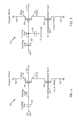
FIG. 1 illustrates a schematic of a PMOS FinFET floating gate NVM cell. Representatively, a memory cell 100 includes a control transistor 102 (also referred to as coupling gate 102), a program transistor 104, and, optionally, an erase transistor 106 (also referred to as an erase gate/capacitor 106). The coupling gate 102, the gate of the program transistor 104, and, optionally, the gate of the erase gate/capacitor 106 are coupled together at the floating gate 108. The drain 110, the source 112, and the well (which may be an n-doped well) 114 are shown for the program transistor 104. There can also be a word line access transistor in series (not shown). This would be a four PMOS transistor floating gate FinFET NVM cell. It also can be a four NMOS transistor floating gate FinFET NVM cell.
As shown in FIG. 2, in an aspect of the present disclosure, the coupling gate 102 is a plate capacitor. To program the program transistor 104, the source 112, which is coupled to a bit line (BL) 202, is brought to a low voltage, which may be ground. In addition, the drain 110, which is coupled to a source line (SL) 200, is brought to a higher voltage, which may be the operating voltage or the supply voltage (Vdd). To turn on the program transistor 104, the voltage across the coupling gate 102 is negative raised, for example, by applying a negative voltage to the word line (WL) or control gate (CG) 206. The word line/control gate 206 is the conduction path of the coupling gate 102. When the coupling gate 102 receives a negative bias, negative charge is induced on the coupling gate 102, inducing negative charge on the floating gate 108 of the program transistor 104. The floating gate 108 may use an n-type conductive gate for PMOS devices for improved data retention. This allows the channel in the program transistor 104 to turn on and conduct. A conducting program gate of the program transistor 104 indicates a particular logic level whereas a non-conducting program gate of the program transistor 104 indicates a different logic level with positive charge inside the floating gate 108. The program floating device can be an NMOS floating gate device. The floating gate 108 may use a p-type conductive gate for NMOS devices for improved data retention. FIG. 2 shows a one transistor floating gate NVM cell.
Another aspect of the present disclosure, shown in FIG. 3, includes the erase gate/capacitor 106 as part of the memory cell 100. When the erase gate/capacitor 106 is biased by voltage of the erase gate/capacitor 106, in optional conjunction with changing the voltage on the word line/control gate 206, the charge at the floating gate 108 is reduced such that the program transistor 104 no longer has enough electrical charge on the floating gate 108 to shut off current between the source line 200 and the bit line 202. The floating gate 108 may use an n-type conductive gate for PMOS devices for better data retention. This “erases” the program transistor 104. The program floating device can also be an NMOS floating gate device. The floating gate 108 may use a p-type conductive gate for NMOS devices for better data retention. The program floating device can also be an NMOS floating gate device. The floating gate 108 may use a p-type conductive gate for NMOS devices for improved data retention. FIG. 3 shows a two transistor floating gate NVM cell.
FIGS. 4 and 5 illustrate schematics of other aspects of PMOS floating gate NVM cells in accordance with the present disclosure.
As shown in FIG. 4, the control gate (CG) 400 may be separated from the word line gate 406 (as opposed to being a combined word line/control gate 206 as shown in FIG. 2) by including an access transistor 402 coupled to the source 112 of the program transistor 104. The bit line 202 is then coupled to the source of the access transistor 402, and the word line gate 406 is coupled to the gate of the access transistor 402. FIG. 4 shows a two transistor floating gate NVM cell.
As shown in FIG. 5, the schematic of FIG. 4 can include an erase gate/capacitor 106. FIG. 5 shows a four transistor floating gate NVM cell. The floating gate 108 may use an n-type conductive gate for PMOS devices for better data retention. The program floating device can also be an NMOS floating gate device. The floating gate 108 may use a p-type conductive gate for NMOS devices for better data retention.
FIG. 6A illustrates a cutaway view of a FinFET floating gate transistor in accordance with an aspect of the present disclosure. Representatively, a substrate 600 supporting an n-well 602 is shown (for PMOS devices). An oxide layer 604, which may be a shallow trench isolation (STI) oxide layer 604, is coupled to the substrate 600 and a portion of the oxide layer 604 is opened to expose the n-well 602. A fin structure 606 with a width and a height is formed, and a gate oxide layer 608 is formed around the fin structure 606. The gate oxide layer 608 may be silicon oxide, or may be a dielectric or other material with a different dielectric constant (k) than silicon oxide, such as Aluminum Oxide, Hafnium Oxide, Hafnium Oxide Nitride, Zirconium Oxide, laminates and/or alloys of these materials. Other materials may be used without departing from the scope of the present disclosure.
A thickness-adjustable oxide may also be coupled to the gate oxide layer 608. Further, the gate oxide layer 608 may be a high-k dielectric material. A “high-k dielectric material” is a dielectric material with a dielectric constant k greater than the dielectric constant of silicon dioxide. For the same actual thickness, a high-k material will provide more capacitance per unit area than silicon dioxide. The high-k gate dielectric film may be made of, for example, Silicon Nitride (SiN), Silicon Carbide (SiC), Aluminum Oxide (Al2O3), Hafnium Oxide (HfOx), Hafnium Oxide Nitride, Zirconium Oxide, combinations or laminations of these or other materials, etc. These materials are used by standard logic FinFET processes and also used in FinFET floating gate devices in the memory cell 100. Use of high-K materials may also improve logic device performance for scaling technology, be used in a multiple time programmable memory, such as the memory cell 100.
As channel sizes in transistors become smaller, the thickness of the dielectric region in the gate oxide layer 608, and the thickness of a coupling film 610, is often reduced. The dielectric constant k of the gate oxide layer 608, along with the thickness of the gate oxide layer 608, has a heightened effect on the control of the floating gate 108 over the channel of the program transistor 104 (between the source 112 and the drain 110)(FIG. 1).
A high-k material allows for higher capacitance across the width of the material. Therefore, a high-k material can be used with a smaller channel size. The increased capacitive coupling accommodates the smaller channel size, allowing the gate to maintain the appropriate influence over the channel of the transistor. A larger actual thickness of a high-k material helps reduce or even minimize leakage current in the transistor.
A floating gate 108 is formed around the gate oxide layer 608. The floating gate 108 is conductive, and may be metal, polysilicon, or other materials. The coupling film 610, which is also referred to as a cap layer, is then placed on the floating gate 108. The coupling film 610 may be a dielectric, or other insulator as specified. The coupling gate 102 is then placed on the coupling film 610. A source contact 612, a drain contact 614, and a coupling gate contact 616 are then deposited on the source 112, the drain 110, and the coupling gate 102, respectively.
The fin structure 606 has a width W and a height H. As the voltages on the coupling gate contact 616 (which may be coupled to the word line/control gate 206), drain contact 614 (which is coupled to the source line 200), source contact 612 (which is coupled to the bit line 202) are changed, capacitive coupling occurs between the coupling gate 102 and the floating gate 108. The capacitive coupling allows conduction between the source contact 612 and the drain contact 614.
FIG. 6B illustrates a birds-eye view of a FinFET floating gate transistor in accordance with another aspect of the present disclosure. FIG. 6B illustrates that the coupling gate 102 may wrap around the floating gate 108 in an aspect of the present disclosure. The additional surface area between the coupling gate 102 and the floating gate 108 increases coupling ratio and decreases the amount of voltage specified to induce charge on the floating gate 108.
FIG. 7A illustrates a cutaway of the structure shown in FIG. 6A. Representatively, the gate oxide layer 608 is shown surrounding the fin structure 606, and dielectric layer 700, which may be an inter-layer dielectric (ILD) layer, is shown. Another layer 702, which may be a dielectric layer, insulating layer, or interconnection layer is also shown on the coupling gate 102.
FIG. 7B illustrates a cutaway view of a FinFET floating gate transistor as shown in FIG. 6B. In this configuration, the offset nature of the coupling gate 102 with respect to the fin structure 606 illustrates that the channel between the source 112 and the drain 110 is controllable with the coupling gate 102. Control of the channel between the source 112 and the drain 110 is possible even when the coupling gate 102 is not in line with the fin structure 606. The coupling gate 102 generates charge on the floating gate 108 that controls the channel between the source 112 and the drain 110.
FIG. 8 illustrates a cutaway view of another FinFET floating gate transistor including an erase capacitor structure in accordance with an aspect of the present disclosure. Representatively, floating gate transistors 800 and 802 are illustrated. Similar to the structure shown in FIG. 6, the substrate 600 is shown, with a p-well 804 (for NMOS devices). An n-well 602 similar to that shown in FIG. 6 may be used without departing from the scope of the present disclosure. A fin structure 606 is shown, with the floating gate 108 and the gate oxide layer 608. The coupling gate 102 and coupling gate contact 616, which is part of “metal layer 0,” is shown.
An erase capacitor oxide 806 and erase capacitor contact 808 are also shown in between the floating gate transistors 800 and 802. In this configuration, the floating gate transistors 800 and 802 are FinFET versions of the program transistor 104, and the erase capacitor oxide 806 is an example of the erase gate/capacitor 106. Nevertheless, other configurations of the program transistor 104, which may be a CMOS transistor without a FinFET structure, and other configurations of the erase gate/capacitor 106, are envisioned to be within the scope of the present disclosure.
FIG. 9 illustrates a cutaway view of a FinFET structure in an aspect of the present disclosure. In particular, as shown in FIG. 9, the coupling gate 102 and the coupling gate contact 616 for the floating gate transistors 800 and 802 are shown. A spacer layer 900 is shown to provide an optionally different capacitive coupling between the sides of the coupling gate 102 and the sides of the floating gate 108. To program, read, and erase the floating gate transistors 800 and 802, voltages on the coupling gate 102 (which is coupled to the coupling gate contact 616), the word line/control gate 206, the bit line 202, the source line 200 (as shown in FIG. 2), and the erase gate/capacitor 106 (which is coupled to the erase capacitor contact 808) are selectively controlled to store or remove charge on the floating gate 108.
For example, and not by way of limitation, to program the floating gate transistor 802, the word line/control gate 206 is brought to a high voltage, which may be the supply voltage Vcc. This puts charge carriers into the fin structure 606 from an NMOS access word line (e.g., the word line/control gate 206). The source line is brought to a programming voltage, which may be between 1 and 4 volts. The control gate (CG) 400 (or the coupling gate contact 616) coupled to the coupling gate 102 is brought to a programming voltage, which may be approximately 4˜10 volts. The erase capacitor contact 808 is brought to a programming voltage, which may be similar to the voltage on the source line 200. These voltages allow for current to flow through the floating gate transistor 802, and hot electron injection allows for charge to inject into the floating gate 108. The electric charge injection direction 902 between the fin structure 606 and the floating gate 108 is shown. Once the floating gate 108 is charged, the voltages can be selectively removed and the charge is stored on the floating gate 108.
To erase a floating gate transistor 802 that is programmed, the erase capacitor contact 808 is brought to an erase voltage, which may be approximately 6 to 10 volts. The word line/control gate 206, the source line 200, the bit line 202, and the control gate/capacitor 400 are all brought to a low voltage, which may be zero volts. This difference in voltage potentials allows for Fowler-Nordheim (FN) tunneling of the charge carriers stored on the floating gate 108 to migrate across the erase capacitor oxide 806 to the erase capacitor contact 808. The FN path 906 for erasure of the floating gate transistor 802 is shown. Similar actions occur for writing to and erasing from the floating gate transistor 800. An additional layer 908 of dielectric or other material may be applied to planarize or otherwise seal the structure if specified, such that other manufacturing processes may be performed on the structure shown in FIG. 9. FIG. 10 illustrates that the cap layer 904 may reside between the coupling gate 102 and the coupling film 610. The cap layer 904 and the coupling film 610 may be dielectrics or other insulators as specified.
FIG. 11 illustrates a cutaway view of an NMOS floating gate and word line access transistors in accordance with an aspect of the present disclosure. When the structure of FIG. 8 is cutaway along the Y-Y′ line, the view of FIG. 11 is seen. The substrate 600 and p-well 804 are shown, and the fin structure 606 shows a fin channel 1100 between the drain 110 and the source 112. As voltage is applied to the coupling gate contact 616, electric fields are generated in the fin channel 1100. Depending on the voltages present on the source line 200, the bit line 202, and the word line/control gate 206, current will flow between the source 112 and the drain 110. The cutaway view of FIG. 11 includes the access transistor 402, as the word line/control gate 206 and the coupling gate contact 616 are separated.
FIGS. 12 through 15 illustrate a process construction flow of transistors in accordance with an aspect of the present disclosure. FIG. 12 illustrates initial steps of depositing layers on the fin structure 606. The gate oxide layer 608, which may be a high-k dielectric material, is coupled to the fin structure 606, and the floating gate 108. An opening 1200 is made near the floating gate transistor 800, and a layer 1202 of material, which may be a section of the floating gate material is deposited. The spacer layer 900 is also deposited and etched or otherwise manipulated to conform the spacer layer 900 around the fin structure 606.
FIG. 13 illustrates addition of the coupling film 610, and the coupling gate 102, to the floating gate transistor 800. Because the material used for the coupling gate 102 is often conductive, a layer 1300 of this material, or other material, is deposited on the layer 1202 and in the opening 1200 for the erase contact.
FIG. 14 shows the erase connection 1400 and the cap layer 904, with the dielectric layer 700 as a planarizing and/or isolation material such that the cap layer 904 is substantially planar and electrical contacts are isolated from each other as specified. The planarization allows for additional processing of the floating gate transistor 800.
FIG. 15 illustrates addition of the coupling gate contact 616 and the erase capacitor contact 808. Additionally the layer 908 may be added, again for planarization and/or isolation of the contacts as specified. Additional layers, such as interconnections, vias, or other electronic circuitry may be added to the floating gate transistor 800 as specified.
FIG. 16 illustrates an operation control table in accordance with an aspect of the present disclosure. To program a particular transistor, voltages are set for certain operations 1600. The word line/control gate 206, the source line 200, the control gate/capacitor 400, erase gate/capacitor 106, and the bit line 202 are controlled based on the selected operation 1600. A read operation 1602, a programming operation 1604, and an erase operation 1606 may be performed. Voltages that may be applied to the lines are shown for when a given transistor is selected or unselected for the operations used in NVM cells, including MTP memory cells of the present disclosure.
FIG. 17 illustrates a process flow in accordance with an aspect of the present disclosure. Representatively, a flow chart 1700 illustrates a method of fabricating a multiple time programmable (MTP) NVM device. At block 1702, fins of a first conducting type are formed on a substrate of a second conducting type, as shown, for example, in FIG. 6. At block 1704, a floating gate dielectric is formed to partially surround the fins.
At block 1706, a floating gate is formed on the floating gate dielectric. At block 1708, a coupling film is formed on the floating gate. At block 1710, a coupling gate is formed on the coupling film.
Aspects of the present disclosure provides advantages over the related art by using a high-k/metal gate process to form an floating gate type eFlash MTP cell. Further, one aspect of the present disclosure allows the use of FinFET structures within an MTP cell. The structures, according to one aspect of the present disclosure, use similar processing as related devices. This aspect of present disclosure allows for a thickness tunable coupling oxide/high-k film, which may reduce the erase voltage used and improve data retention in the MTP cell. The control voltage of coupling gate 102 on the floating gate 108 can be positive or negative, whereas the related art used a positive voltage on the floating gate 108.
Aspects of the present disclosure also allow for additional coupling of the FinFET structure by “wrapping” the floating gate 108 and the coupling gate 102 around the fin structure 606 as shown in FIG. 15. This increased coupling allows for lower programming (write) voltages in the FinFET structure of this aspect of the present disclosure. Again, the control voltage of coupling gate 102 on the floating gate 108 can be positive or negative in this aspect of the present disclosure, eliminating the positive-only control of the related art.
In one configuration, a multiple time programmable (MTP) device includes a means for conducting current. In one aspect of the disclosure, the current conducting means may be the fin structure 606, the source 112 and the drain 110 and/or other structures configured to perform the transistor functions recited by the current conducting means. In this configuration, the device also includes means for storing charges. In one aspect, the storing means may be the floating gate 108 and/or other structures configured to perform the transistor functions recited by the current controlling means. The device also includes means for controlling logic states. The controlling means can be the coupling gate 102 and/or other structures configured to perform the functions recited by the charge inducing means. In another aspect, the aforementioned means may be any module or any apparatus configured to perform the functions recited by the aforementioned means.
FIG. 18 is a block diagram showing an exemplary wireless communication system 1800 in which an aspect of the disclosure may be advantageously employed. For purposes of illustration, FIG. 18 shows three remote units 1820, 1830, and 1850 and two base stations 1840. It will be recognized that wireless communication systems may have many more remote units and base stations. Remote units 1820, 1830, and 1850 include IC devices 1825A, 1825C, and 1825B that include the floating gate transistors 800 and 802 or other disclosed structures in the present disclosure. It will be recognized that other devices may also include the disclosed devices, such as the base stations, switching devices, and network equipment. FIG. 18 shows forward link signals 1880 from the base station 1840 to the remote units 1820, 1830, and 1850 and reverse link signals 1890 from the remote units 1820, 1830, and 1850 to base stations 1840.
In FIG. 18, remote unit 1820 is shown as a mobile telephone, remote unit 1830 is shown as a portable computer, and remote unit 1850 is shown as a fixed location remote unit in a wireless local loop system. For example, the remote units may be mobile phones, hand-held personal communication systems (PCS) units, portable data units such as personal data assistants, GPS enabled devices, navigation devices, set top boxes, music players, video players, entertainment units, fixed location data units such as meter reading equipment, or other devices that store or retrieve data or computer instructions, or combinations thereof. Although FIG. 18 illustrates remote units according to the aspects of the disclosure, the disclosure is not limited to these exemplary illustrated units. Aspects of the disclosure may be suitably employed in many devices, which include the disclosed transistors, FinFETs, or other structures within the scope of the present disclosure.
Those of skill would further appreciate that the various illustrative logical blocks, modules, circuits, and algorithm steps described in connection with the disclosure herein may be implemented as electronic hardware, computer software, or combinations of both. To clearly illustrate this interchangeability of hardware and software, various illustrative components, blocks, modules, circuits, and steps have been described above generally in terms of their functionality. Whether such functionality is implemented as hardware or software depends upon the particular application and design constraints imposed on the overall system. Skilled artisans may implement the described functionality in varying ways for each particular application, but such implementation decisions should not be interpreted as causing a departure from the scope of the present disclosure.
The various illustrative logical blocks, modules, and circuits described in connection with the disclosure herein may be implemented or performed with a general-purpose processor, a digital signal processor (DSP), an application specific integrated circuit (ASIC), a field programmable gate array (FPGA) or other programmable logic device, discrete gate or transistor logic, discrete hardware components, or any combination thereof designed to perform the functions described herein. A general-purpose processor may be a microprocessor, but in the alternative, the processor may be any conventional processor, controller, microcontroller, or state machine. A processor may also be implemented as a combination of computing devices, e.g., a combination of a DSP and a microprocessor, multiple microprocessors, one or more microprocessors in conjunction with a DSP core, or any other such configuration.
The steps of a method or algorithm described in connection with the disclosure may be embodied directly in hardware, in a software module executed by a processor, or in a combination of the two. A software module may reside in RAM memory, flash memory, ROM, EPROM, EEPROM, registers, hard disk, a removable disk, a CD-ROM, or any other form of storage medium known in the art. An exemplary storage medium is coupled to the processor such that the processor can read information from, and write information to, the storage medium. In the alternative, the storage medium may be integral to the processor. The processor and the storage medium may reside in an ASIC. The ASIC may reside in a user terminal. In the alternative, the processor and the storage medium may reside as discrete components in a user terminal.
In one or more exemplary designs, the functions described may be implemented in hardware, software, firmware, or any combination thereof. If implemented in software, the functions may be stored on or transmitted over as one or more instructions or code on a computer-readable medium. Computer-readable media includes both computer storage media and communication media including any medium that facilitates transfer of a computer program from one place to another. A storage media may be any available media that can be accessed by a general purpose or special purpose computer. By way of example, and not limitation, such computer-readable media can include RAM, ROM, EEPROM, CD-ROM or other optical disk storage, magnetic disk storage or other magnetic storage devices, or any other medium that can be used to carry or store specified program code means in the form of instructions or data structures and that can be accessed by a general-purpose or special-purpose computer, or a general-purpose or special-purpose processor. Also, any connection is properly termed a computer-readable medium. For example, if the software is transmitted from a website, server, or other remote source using a coaxial cable, fiber optic cable, twisted pair, digital subscriber line (DSL), or wireless technologies such as infrared, radio, and microwave, then the coaxial cable, fiber optic cable, twisted pair, DSL, or wireless technologies such as infrared, radio, and microwave are included in the definition of medium. Disk and disc, as used herein, includes compact disc (CD), laser disc, optical disc, digital versatile disc (DVD), floppy disk and Blu-ray disc where disks usually reproduce data magnetically, while discs reproduce data optically with lasers. Combinations of the above should also be included within the scope of computer-readable media.
The previous description of the disclosure is provided to enable any person skilled in the art to make or use the disclosure. Various modifications to the disclosure will be readily apparent to those skilled in the art, and the generic principles defined herein may be applied to other variations without departing from the spirit or scope of the disclosure. Thus, the disclosure is not intended to be limited to the examples and designs described herein but is to be accorded the widest scope consistent with the principles and novel features disclosed herein.

Claims (7)

What is claimed is:
1. A multiple time programmable (MTP) device, comprising:
a substrate including a shallow trench isolation (STI) layer;
a fin having a first wall, a second wall, and a surface connecting the first wall and the second wall, the first wall and the second wall adjoining the STI layer of
the substrate;
a floating gate dielectric having a first dielectric surface on the first wall of the fin, a second dielectric surface on the surface of the fin, and a third dielectric surface on the second wall of the fin;
a dielectric spacer on the first dielectric surface and the second dielectric surface of the floating gate dielectric;
a floating gate on the floating gate dielectric and the dielectric spacer;
a coupling film in which an entire length of the coupling film is on an entire length of the floating gate; and
a coupling gate on the entire length of the coupling film and at least a portion of the coupling gate directly coupled to the STI layer of the substrate.
2. The MTP device of claim 1, in which the floating gate is directly coupled to the floating gate dielectric on the second dielectric surface.
3. The MTP device of claim 1, in which the coupling film and coupling gate partially surround the floating gate.
4. The MTP device of claim 1, in which the floating gate comprises an input/output (I/O) device and, the floating gate dielectric comprises a thickness-adjustable oxide.
5. The MTP device of claim 1, in which the floating gate dielectric has a dielectric constant greater than a dielectric constant of silicon oxide.
6. The MTP device of claim 1, further comprising an erase dielectric coupled to the floating gate.
7. The MTP device of claim 1, integrated into a mobile phone, a set top box, a music player, a video player, an entertainment unit, a navigation device, a computer, a hand-held personal communication systems (PCS) unit, a portable data unit, and/or a fixed location data unit.
US14/044,725 2013-07-31 2013-10-02 Logic finFET high-K/conductive gate embedded multiple time programmable flash memory Active US9406689B2 (en)

Priority Applications (5)

Application Number Priority Date Filing Date Title
US14/044,725 US9406689B2 (en) 2013-07-31 2013-10-02 Logic finFET high-K/conductive gate embedded multiple time programmable flash memory
CN201480043155.1A CN105431944B (en) 2013-07-31 2014-06-12 Logic FINFET high-K/conductive gate embedded multi-time programmable flash memory
PCT/US2014/042142 WO2015017030A1 (en) 2013-07-31 2014-06-12 Logic finfet high-k/conductive gate embedded multiple time programmable flash memory
EP14736226.3A EP3028309B1 (en) 2013-07-31 2014-06-12 Logic finfet high-k/conductive gate embedded multiple time programmable flash memory
US15/194,125 US20160308062A1 (en) 2013-07-31 2016-06-27 Logic finfet high-k/conductive gate embedded multiple time programmable flash memory

Applications Claiming Priority (2)

Application Number Priority Date Filing Date Title
US201361860481P 2013-07-31 2013-07-31
US14/044,725 US9406689B2 (en) 2013-07-31 2013-10-02 Logic finFET high-K/conductive gate embedded multiple time programmable flash memory

Related Child Applications (1)

Application Number Title Priority Date Filing Date
US15/194,125 Division US20160308062A1 (en) 2013-07-31 2016-06-27 Logic finfet high-k/conductive gate embedded multiple time programmable flash memory

Publications (2)

Publication Number Publication Date
US20150035039A1 US20150035039A1 (en) 2015-02-05
US9406689B2 true US9406689B2 (en) 2016-08-02

Family

ID=52426881

Family Applications (2)

Application Number Title Priority Date Filing Date
US14/044,725 Active US9406689B2 (en) 2013-07-31 2013-10-02 Logic finFET high-K/conductive gate embedded multiple time programmable flash memory
US15/194,125 Abandoned US20160308062A1 (en) 2013-07-31 2016-06-27 Logic finfet high-k/conductive gate embedded multiple time programmable flash memory

Family Applications After (1)

Application Number Title Priority Date Filing Date
US15/194,125 Abandoned US20160308062A1 (en) 2013-07-31 2016-06-27 Logic finfet high-k/conductive gate embedded multiple time programmable flash memory

Country Status (4)

Country Link
US (2) US9406689B2 (en)
EP (1) EP3028309B1 (en)
CN (1) CN105431944B (en)
WO (1) WO2015017030A1 (en)

Cited By (14)

* Cited by examiner, † Cited by third party
Publication number Priority date Publication date Assignee Title
US20160218222A1 (en) * 2013-12-11 2016-07-28 Globalfoundries Inc. Finfet crosspoint flash memory
US20170133391A1 (en) * 2014-06-20 2017-05-11 Floadia Corporation Non-Volatile Semiconductor Memory Device
US9691907B1 (en) * 2016-07-06 2017-06-27 United Microelectronics Corp. Non-volatile memory device and manufacturing method thereof
US20180082728A1 (en) * 2016-09-16 2018-03-22 Micron Technology, Inc. Compensation for threshold voltage variation of memory cell components
US9972630B2 (en) 2015-11-03 2018-05-15 Silicon Storage Technology, Inc. Split gate non-volatile flash memory cell having metal gates and method of making same
US10269437B2 (en) * 2017-05-01 2019-04-23 Copee Technology Company Non-volatile memory device and operation method of the same
US10312247B1 (en) * 2018-03-22 2019-06-04 Silicon Storage Technology, Inc. Two transistor FinFET-based split gate non-volatile floating gate flash memory and method of fabrication
US10468428B1 (en) 2018-04-19 2019-11-05 Silicon Storage Technology, Inc. Split gate non-volatile memory cells and logic devices with FinFET structure, and method of making same
US10644012B2 (en) 2018-07-05 2020-05-05 Silicon Storage Technology, Inc. Method of making split gate non-volatile memory cells with three-dimensional FinFET structure, and method of making same
US10797142B2 (en) 2018-12-03 2020-10-06 Silicon Storage Technology, Inc. FinFET-based split gate non-volatile flash memory with extended source line FinFET, and method of fabrication
US10886287B2 (en) 2019-01-14 2021-01-05 Globalfoundries Inc. Multiple-time programmable (MTP) memory device with a wrap-around control gate
US10937794B2 (en) 2018-12-03 2021-03-02 Silicon Storage Technology, Inc. Split gate non-volatile memory cells with FinFET structure and HKMG memory and logic gates, and method of making same
US11081557B2 (en) * 2019-07-29 2021-08-03 Shanghai Huahong Grace Semiconductor Manufacturing Corporation Memory and method for forming the same
US11362100B2 (en) 2020-03-24 2022-06-14 Silicon Storage Technology, Inc. FinFET split gate non-volatile memory cells with enhanced floating gate to floating gate capacitive coupling

Families Citing this family (12)

* Cited by examiner, † Cited by third party
Publication number Priority date Publication date Assignee Title
US9812336B2 (en) * 2013-10-29 2017-11-07 Globalfoundries Inc. FinFET semiconductor structures and methods of fabricating same
US9428664B2 (en) 2014-10-02 2016-08-30 Xerox Corporation Undercoat layer with low release force for aqueous printing transfix system
EP3314664A4 (en) * 2015-06-26 2019-02-20 INTEL Corporation Semi-volatile embedded memory with between-fin floating-gate device and method
US10109641B2 (en) * 2015-08-10 2018-10-23 Toshiba Memory Corporation Semiconductor device and method for manufacturing same
US10978568B2 (en) * 2015-09-25 2021-04-13 Intel Corporation Passivation of transistor channel region interfaces
US10276726B2 (en) * 2016-05-31 2019-04-30 Taiwan Semiconductor Manufacturing Co., Ltd. Non-volatile memory cell and non-volatile memory
US9899485B2 (en) 2016-06-07 2018-02-20 International Business Machines Corporation Spatially decoupled floating gate semiconductor device
US9911867B2 (en) * 2016-07-01 2018-03-06 Globalfoundries Singapore Pte. Ltd. Fin-based nonvolatile memory structures, integrated circuits with such structures, and methods for fabricating same
US9589970B1 (en) * 2016-08-02 2017-03-07 United Microelectronics Corp. Antifuse one-time programmable memory
US9954082B1 (en) 2017-04-25 2018-04-24 United Microelectronics Corp. Method of fabricating an embedded nonvolatile memory device
US11296203B2 (en) * 2017-12-26 2022-04-05 Intel Corporation Switching device having gate stack with low oxide growth
US11114451B1 (en) * 2020-02-27 2021-09-07 Silicon Storage Technology, Inc. Method of forming a device with FinFET split gate non-volatile memory cells and FinFET logic devices

Citations (15)

* Cited by examiner, † Cited by third party
Publication number Priority date Publication date Assignee Title
US7005697B2 (en) 2002-06-21 2006-02-28 Micron Technology, Inc. Method of forming a non-volatile electron storage memory and the resulting device
US20060044915A1 (en) * 2004-09-01 2006-03-02 Park Ji-Hoon Flash memory device using semiconductor fin and method thereof
US20070090443A1 (en) * 2005-10-26 2007-04-26 Samsung Electronics Co., Ltd. Method of fabricating a semiconductor device having self-aligned floating gate and related device
WO2007069180A1 (en) 2005-12-15 2007-06-21 Nxp B.V. Non-volatile memory device having a gap in the tunnuel insulating layer and method of manufacturing the same
EP1909288A1 (en) 2006-10-03 2008-04-09 Macronix International Co., Ltd. Cell operation methods using gate-injection for floating gate nand flash memory
US7405968B2 (en) 2004-01-21 2008-07-29 Sandisk Corporation Non-volatile memory cell using high-K material and inter-gate programming
EP2026378A2 (en) 2007-08-13 2009-02-18 Samsung Electronics Co., Ltd Non-volatile FinFET memory device and method of fabricating the same
US20090184346A1 (en) 2008-01-09 2009-07-23 Jain Faquir C Nonvolatile memory and three-state FETs using cladded quantum dot gate structure
US8068370B2 (en) 2008-04-18 2011-11-29 Macronix International Co., Ltd. Floating gate memory device with interpoly charge trapping structure
US20120299098A1 (en) 2011-05-25 2012-11-29 Taiwan Semiconductor Manufacturing Company, Ltd. Fin-like field effect transistor (finfet) non-volatile random access memory (nvram) device with bottom erase gate
US20120313097A1 (en) * 2005-04-26 2012-12-13 Micron Technology, Inc. Flash memory device having a graded composition, high dielectric constant gate insulator
US8334560B2 (en) * 2009-09-02 2012-12-18 Taiwan Semiconductor Manufacturing Company, Ltd. Reverse disturb immune asymmetrical sidewall floating gate devices
US8440542B2 (en) 2010-10-11 2013-05-14 Monolithic 3D Inc. Semiconductor device and structure
US20140191323A1 (en) * 2013-01-08 2014-07-10 International Business Machines Corporation Method of forming finfet of variable channel width
US20160104801A1 (en) * 2013-05-03 2016-04-14 Institute Of Microlectronics, Chinese Academy Of Sciences Memory devices, methods of manufacturing the same, and methods of accessing the same

Family Cites Families (2)

* Cited by examiner, † Cited by third party
Publication number Priority date Publication date Assignee Title
US6958512B1 (en) * 2004-02-03 2005-10-25 Advanced Micro Devices, Inc. Non-volatile memory device
US7535060B2 (en) * 2006-03-08 2009-05-19 Freescale Semiconductor, Inc. Charge storage structure formation in transistor with vertical channel region

Patent Citations (17)

* Cited by examiner, † Cited by third party
Publication number Priority date Publication date Assignee Title
US7005697B2 (en) 2002-06-21 2006-02-28 Micron Technology, Inc. Method of forming a non-volatile electron storage memory and the resulting device
US7405968B2 (en) 2004-01-21 2008-07-29 Sandisk Corporation Non-volatile memory cell using high-K material and inter-gate programming
US20060044915A1 (en) * 2004-09-01 2006-03-02 Park Ji-Hoon Flash memory device using semiconductor fin and method thereof
US20120313097A1 (en) * 2005-04-26 2012-12-13 Micron Technology, Inc. Flash memory device having a graded composition, high dielectric constant gate insulator
US7329580B2 (en) * 2005-10-26 2008-02-12 Samsung Electronics Co., Ltd. Method of fabricating a semiconductor device having self-aligned floating gate and related device
US20070090443A1 (en) * 2005-10-26 2007-04-26 Samsung Electronics Co., Ltd. Method of fabricating a semiconductor device having self-aligned floating gate and related device
WO2007069180A1 (en) 2005-12-15 2007-06-21 Nxp B.V. Non-volatile memory device having a gap in the tunnuel insulating layer and method of manufacturing the same
EP1909288A1 (en) 2006-10-03 2008-04-09 Macronix International Co., Ltd. Cell operation methods using gate-injection for floating gate nand flash memory
US8325530B2 (en) * 2006-10-03 2012-12-04 Macronix International Co., Ltd. Cell operation methods using gate-injection for floating gate NAND flash memory
EP2026378A2 (en) 2007-08-13 2009-02-18 Samsung Electronics Co., Ltd Non-volatile FinFET memory device and method of fabricating the same
US20090184346A1 (en) 2008-01-09 2009-07-23 Jain Faquir C Nonvolatile memory and three-state FETs using cladded quantum dot gate structure
US8068370B2 (en) 2008-04-18 2011-11-29 Macronix International Co., Ltd. Floating gate memory device with interpoly charge trapping structure
US8334560B2 (en) * 2009-09-02 2012-12-18 Taiwan Semiconductor Manufacturing Company, Ltd. Reverse disturb immune asymmetrical sidewall floating gate devices
US8440542B2 (en) 2010-10-11 2013-05-14 Monolithic 3D Inc. Semiconductor device and structure
US20120299098A1 (en) 2011-05-25 2012-11-29 Taiwan Semiconductor Manufacturing Company, Ltd. Fin-like field effect transistor (finfet) non-volatile random access memory (nvram) device with bottom erase gate
US20140191323A1 (en) * 2013-01-08 2014-07-10 International Business Machines Corporation Method of forming finfet of variable channel width
US20160104801A1 (en) * 2013-05-03 2016-04-14 Institute Of Microlectronics, Chinese Academy Of Sciences Memory devices, methods of manufacturing the same, and methods of accessing the same

Non-Patent Citations (1)

* Cited by examiner, † Cited by third party
Title
International Search Report and Written Opinion-PCT/US2014/042142-ISA/EPO-Sep. 17, 2014.

Cited By (21)

* Cited by examiner, † Cited by third party
Publication number Priority date Publication date Assignee Title
US9660105B2 (en) * 2013-12-11 2017-05-23 Globalfoundries Inc. Finfet crosspoint flash memory
US20160218222A1 (en) * 2013-12-11 2016-07-28 Globalfoundries Inc. Finfet crosspoint flash memory
US10680001B2 (en) * 2014-06-20 2020-06-09 Floadia Corporation Non-volatile semiconductor memory device
US20170133391A1 (en) * 2014-06-20 2017-05-11 Floadia Corporation Non-Volatile Semiconductor Memory Device
US9972630B2 (en) 2015-11-03 2018-05-15 Silicon Storage Technology, Inc. Split gate non-volatile flash memory cell having metal gates and method of making same
US10249631B2 (en) 2015-11-03 2019-04-02 Silicon Storage Technology, Inc. Split gate non-volatile flash memory cell having metal gates
US9691907B1 (en) * 2016-07-06 2017-06-27 United Microelectronics Corp. Non-volatile memory device and manufacturing method thereof
US20180082728A1 (en) * 2016-09-16 2018-03-22 Micron Technology, Inc. Compensation for threshold voltage variation of memory cell components
US10153019B2 (en) * 2016-09-16 2018-12-11 Micron Technology, Inc. Compensation for threshold voltage variation of memory cell components
US10607675B2 (en) 2016-09-16 2020-03-31 Micron Technology, Inc. Compensation for threshold voltage variation of memory cell components
US10269437B2 (en) * 2017-05-01 2019-04-23 Copee Technology Company Non-volatile memory device and operation method of the same
US10312247B1 (en) * 2018-03-22 2019-06-04 Silicon Storage Technology, Inc. Two transistor FinFET-based split gate non-volatile floating gate flash memory and method of fabrication
US10468428B1 (en) 2018-04-19 2019-11-05 Silicon Storage Technology, Inc. Split gate non-volatile memory cells and logic devices with FinFET structure, and method of making same
US10818680B2 (en) 2018-04-19 2020-10-27 Silicon Storage Technology, Inc. Split gate non-volatile memory cells and logic devices with FINFET structure, and method of making same
US10644012B2 (en) 2018-07-05 2020-05-05 Silicon Storage Technology, Inc. Method of making split gate non-volatile memory cells with three-dimensional FinFET structure, and method of making same
US10727240B2 (en) 2018-07-05 2020-07-28 Silicon Store Technology, Inc. Split gate non-volatile memory cells with three-dimensional FinFET structure
US10797142B2 (en) 2018-12-03 2020-10-06 Silicon Storage Technology, Inc. FinFET-based split gate non-volatile flash memory with extended source line FinFET, and method of fabrication
US10937794B2 (en) 2018-12-03 2021-03-02 Silicon Storage Technology, Inc. Split gate non-volatile memory cells with FinFET structure and HKMG memory and logic gates, and method of making same
US10886287B2 (en) 2019-01-14 2021-01-05 Globalfoundries Inc. Multiple-time programmable (MTP) memory device with a wrap-around control gate
US11081557B2 (en) * 2019-07-29 2021-08-03 Shanghai Huahong Grace Semiconductor Manufacturing Corporation Memory and method for forming the same
US11362100B2 (en) 2020-03-24 2022-06-14 Silicon Storage Technology, Inc. FinFET split gate non-volatile memory cells with enhanced floating gate to floating gate capacitive coupling

Also Published As

Publication number Publication date
EP3028309A1 (en) 2016-06-08
CN105431944A (en) 2016-03-23
CN105431944B (en) 2020-01-03
US20160308062A1 (en) 2016-10-20
US20150035039A1 (en) 2015-02-05
EP3028309B1 (en) 2020-03-25
WO2015017030A1 (en) 2015-02-05

Similar Documents

Publication Publication Date Title
US9406689B2 (en) Logic finFET high-K/conductive gate embedded multiple time programmable flash memory
US11672124B2 (en) High voltage CMOS with co-planar upper gate surfaces for embedded non-volatile memory
US9640259B2 (en) Single-poly nonvolatile memory cell
US8120095B2 (en) High-density, trench-based non-volatile random access SONOS memory SOC applications
US20160005749A1 (en) Series ferroelectric negative capacitor for multiple time programmable (mtp) devices
US6903968B2 (en) Nonvolatile memory capable of storing multibits binary information and the method of forming the same
US8878281B2 (en) Methods and apparatus for non-volatile memory cells
US7872295B2 (en) Method of making flash memory cells and peripheral circuits having STI, and flash memory devices and computer systems having the same
US20080258203A1 (en) Stacked sonos memory
US7638835B2 (en) Double density NROM with nitride strips (DDNS)
US20130242659A1 (en) Split-gate type nonvolatile memory device, semiconductor device having split-type nonvolatile memory device embedded therein, and methods of forming the same
US9634017B1 (en) Semiconductor structure including a nonvolatile memory cell and method for the formation thereof
US20140264554A1 (en) Back-gated non-volatile memory cell
TW201301485A (en) Non-volatile semiconductor memory cell with dual functions
US9166013B2 (en) Nonvolatile memory device and method for fabricating the same
US8476690B2 (en) Nonvolatile programmable logic switches and semiconductor integrated circuit
JP2008010868A (en) Nonvolatile memory device having vertical channel and manufacturing method of the same
US9252150B1 (en) High endurance non-volatile memory cell
TW201131743A (en) Two pFET SOI memory cells
CN103999194B (en) With the capacity coupled nonvolatile memory device of vertical drain-to-gate

Legal Events

Date Code Title Description
AS Assignment

Owner name: QUALCOMM INCORPORATED, CALIFORNIA

Free format text: ASSIGNMENT OF ASSIGNORS INTEREST;ASSIGNORS:LI, XIA;YANG, BIN;KANG, SEUNG HYUK;REEL/FRAME:031368/0501

Effective date: 20131003

STCF Information on status: patent grant

Free format text: PATENTED CASE

MAFP Maintenance fee payment

Free format text: PAYMENT OF MAINTENANCE FEE, 4TH YEAR, LARGE ENTITY (ORIGINAL EVENT CODE: M1551); ENTITY STATUS OF PATENT OWNER: LARGE ENTITY

Year of fee payment: 4

FEPP Fee payment procedure

Free format text: MAINTENANCE FEE REMINDER MAILED (ORIGINAL EVENT CODE: REM.); ENTITY STATUS OF PATENT OWNER: LARGE ENTITY