US9337446B2 - Encapsulated RGB OLEDs having enhanced optical output - Google Patents
Encapsulated RGB OLEDs having enhanced optical output Download PDFInfo
- Publication number
- US9337446B2 US9337446B2 US12/341,134 US34113408A US9337446B2 US 9337446 B2 US9337446 B2 US 9337446B2 US 34113408 A US34113408 A US 34113408A US 9337446 B2 US9337446 B2 US 9337446B2
- Authority
- US
- United States
- Prior art keywords
- oled
- layer
- thickness
- barrier layer
- inorganic barrier
- Prior art date
- Legal status (The legal status is an assumption and is not a legal conclusion. Google has not performed a legal analysis and makes no representation as to the accuracy of the status listed.)
- Active, expires
Links
Images


Classifications
-
- H01L51/5275—
-
- H01L51/5237—
-
- H—ELECTRICITY
- H10—SEMICONDUCTOR DEVICES; ELECTRIC SOLID-STATE DEVICES NOT OTHERWISE PROVIDED FOR
- H10K—ORGANIC ELECTRIC SOLID-STATE DEVICES
- H10K50/00—Organic light-emitting devices
- H10K50/80—Constructional details
- H10K50/84—Passivation; Containers; Encapsulations
-
- H—ELECTRICITY
- H10—SEMICONDUCTOR DEVICES; ELECTRIC SOLID-STATE DEVICES NOT OTHERWISE PROVIDED FOR
- H10K—ORGANIC ELECTRIC SOLID-STATE DEVICES
- H10K50/00—Organic light-emitting devices
- H10K50/80—Constructional details
- H10K50/84—Passivation; Containers; Encapsulations
- H10K50/844—Encapsulations
-
- H—ELECTRICITY
- H10—SEMICONDUCTOR DEVICES; ELECTRIC SOLID-STATE DEVICES NOT OTHERWISE PROVIDED FOR
- H10K—ORGANIC ELECTRIC SOLID-STATE DEVICES
- H10K50/00—Organic light-emitting devices
- H10K50/80—Constructional details
- H10K50/85—Arrangements for extracting light from the devices
- H10K50/858—Arrangements for extracting light from the devices comprising refractive means, e.g. lenses
-
- H01L2251/558—
-
- H01L51/5234—
-
- H—ELECTRICITY
- H10—SEMICONDUCTOR DEVICES; ELECTRIC SOLID-STATE DEVICES NOT OTHERWISE PROVIDED FOR
- H10K—ORGANIC ELECTRIC SOLID-STATE DEVICES
- H10K2102/00—Constructional details relating to the organic devices covered by this subclass
- H10K2102/301—Details of OLEDs
- H10K2102/351—Thickness
-
- H—ELECTRICITY
- H10—SEMICONDUCTOR DEVICES; ELECTRIC SOLID-STATE DEVICES NOT OTHERWISE PROVIDED FOR
- H10K—ORGANIC ELECTRIC SOLID-STATE DEVICES
- H10K50/00—Organic light-emitting devices
- H10K50/80—Constructional details
- H10K50/805—Electrodes
- H10K50/82—Cathodes
- H10K50/828—Transparent cathodes, e.g. comprising thin metal layers
Definitions
- the invention relates generally to encapsulated organic light emitting devices (OLEDs), and more particularly to encapsulated red, green, and blue (RGB) OLEDs having improved light outcoupling compared to the bare RGB OLED.
- OLEDs organic light emitting devices
- RGB red, green, and blue
- OLEDs have reached remarkable levels of power efficiencies over the years by lowering the operating voltage and increasing the quantum yield of internal light generation to almost 100% resulting in power efficiencies of more than 120 Lm/Watt for green light (Ultra High Efficiency Green Organic Light-Emitting Devices, Jpn. J. Appl. Phys. 46, p. L10-L12, (2007))
- OLED displays and OLED light sources which are made of pixels or stripes which can emit the primary colors R, G, and B.
- R, G, and B the primary colors of the visible spectrum
- the intensity of the R, G and B pixels can be varied to get the optimal white light to address the lighting requirements for a particular lighting application.
- the white light can be made ‘warmer,’ and by increasing the blue component, the white light will appear to be ‘colder’.
- the high efficiency is a major advantage not only for the use of OLEDs for displays, but also their use as a light source for signage and general lighting purposes.
- a multilayer mirror formed by a quarter-wave stack only enhances one narrow band of wavelengths of light emitted from the OLED.
- the structure in a quarter wave stack is wavelength dependent, which means that the use of the same structure for RGB applications can be problematic. Also, the number of layers needed for an effective quarter wave (QW) stack can be quite high (e.g., 10 layers pairs), which makes it impractical for many commercial applications.
- QW quarter wave
- the OLED emission is generally broad. In a well designed QW stack, it is possible that a portion of the light will not be transmitted.
- Another disadvantage of the structure is that the intensity of the light transmitted by a QW stack is strongly directional, and in general the stack is designed with maximum intensity for forward transmission.
- Optical cavities (single and multiple) have been suggested to enhance the light output of OLED devices. Similarly to QW stacks, optical cavities are wavelength specific. Therefore, a specific design and its accurate implementation are necessary for each wavelength. The emission from a single optical cavity is very angular dependent. Double or triple cavities must be implemented to make the emission independent from the observation point. The implementation is therefore practically difficult and complex and may require a different sequence of layers as well as different thicknesses of the layers in parts of the device.
- OLEDs in flat panel displays and other information display formats are limited by the poor environmental stability of the devices.
- Humidity and oxygen significantly reduce the useful life of most OLEDs.
- these devices are typically fabricated on glass substrates with glass covers laminated on top of the OLED and with the edges sealed to exclude water and oxygen from the active layers.
- FIG. 1A and 1B are graphs showing the effect of encapsulation on I-L curves for an OLED
- FIG. 1C is a graph showing the effect of encapsulation on the I-V curves for an OLED.
- FIG. 2 is a graph showing the effect of the protective layer and initial inorganic barrier layers on intensity and spectral distribution of the emitted light for an encapsulated OLED with an ITO cathode layer.
- FIG. 3A-3B are graphs showing the effect of different protective layers having the same thickness.
- FIG. 4 is a graph showing the effect of various types and thicknesses of cathode layers on intensity and spectral distribution of the emitted light.
- FIG. 5A-5C are graphs showing the effect of the thickness of an initial inorganic barrier layer on intensity and spectral distribution of the emitted light for an OLED with a Ag cathode.
- FIG. 6A-6E are graphs showing the effect of the thickness of the polymeric decoupling layer in the barrier stack on intensity and spectral distribution of the emitted light for an encapsulated OLED with a Ag cathode.
- FIG. 7A-7D are graphs showing the effect of the thickness of the inorganic barrier layer in the barrier stack on intensity and spectral distribution of the emitted light for an encapsulated OLED with a Ag cathode.
- FIG. 8A-8B are graphs showing the optimization of an encapsulated OLED with a Ag cathode.
- FIG. 9 is a graph showing the intentional shifting of light emission for an encapsulated OLED.
- FIG. 10 is a graph comparing the light output for a RBG OLED with and without encapsulation.
- FIG. 11 is a graph comparing the effect of an initial inorganic barrier layer with an initial polymeric layer on intensity and spectral distribution of the emitted light for an encapsulated OLED.
- FIG. 12 is a graph comparing the effect of encapsulating an OLED with a single inorganic barrier layer with multiple barrier stacks.
- FIG. 13 is a graph comparing the effect of encapsulating different OLEDs with the same barrier stack.
- FIG. 14 is an illustration of one embodiment of an encapsulated OLED.
- FIG. 15 is an illustration of another embodiment of an encapsulated OLED.
- FIG. 16 shows randomly oriented dipoles located in an emission layer of an encapsulated OLED.
- the present invention meets that need by providing a method of making an integrated barrier and optical enhancement stack for protecting and improving the light out coupling of an encapsulated OLED.
- the method includes providing an OLED having at least two colors selected from red, green, or blue and a transparent electrode; selecting an initial inorganic barrier layer having a refractive index in a range of about 1.55 to about 2, the initial inorganic barrier layer adjacent to the transparent electrode in the OLED; optimizing a thickness of the initial inorganic barrier layer for the OLED, the thickness being in a range of about 40 nm to about 240 nm; selecting a barrier stack comprising an inorganic barrier layer and a polymeric decoupling layer, the inorganic barrier layer having a refractive index in a range of about 1.55 to about 2, and the polymeric decoupling layer having a refractive index in a range of about 1.4 to about 1.65, the barrier stack adjacent to the initial inorganic barrier layer; and optimizing a thickness of the inorganic barrier layer and the polymeric de
- OLED is a generic term for a light emitting device based on organic materials. Suitable organic materials cover a wide range of materials, including polymers, small molecules, or oligomers. Depending on the organic emissive layer being used, the emission of the OLED can vary in color. By ‘OLED,’ we mean the entire emitting structure which can include one, two, three, or more organic materials which generate different colors.
- the emissive layers of the OLED can contain a thin layer of inorganic quantum dots in a device made with organic layers, or a layer of such quantum dots embedded in an organic layer.
- adjacent we mean next to, but not necessarily directly next to. There can be additional layers intervening between the adjacent layers. In the event that additional layers are used between the adjacent layers, those layers should be optimized as part of the structure using the optical simulation as well.
- the decoupling layer decouples defects between adjacent layers and/or the substrate.
- the processes used to deposit the barrier layers tend to reproduce any defects in the layer they are deposited on. Therefore, defects in or on the substrate or previous layer may be replicated in the deposited barrier layer, which can seriously limit the barrier performance of the films.
- the decoupling layer interrupts the propagation of defects from one layer to the next. This is achieved by reducing the surface imperfections of the substrate or previous layer, so that the subsequently deposited barrier layer or other layer, such as the organic light emitting device, has fewer defects.
- the decoupling layer has improved surface planarity compared to the previous layer.
- the decoupling layers decouple defects in the barrier layers.
- the decoupling layer intervenes between barrier layers so that the defects in one layer are not next to the defects in the subsequent layer. This creates a tortuous path for gas diffusion, helping to improve the barrier properties.
- a decoupling layer which is deposited over the barrier layer may also help to protect the barrier layer from damage during processing or further handling.
- the decoupling layers can be deposited using a vacuum process, such as flash evaporation with in situ polymerization under vacuum, or plasma deposition and polymerization, or atmospheric processes, such as spin coating, ink jet printing, screen printing, or spraying.
- the decoupling layer can be made of any suitable decoupling material, including, but not limited to, organic polymers, inorganic polymers, organometallic polymers, hybrid organic/inorganic polymer systems, and combinations thereof.
- Organic polymers include, but are not limited to, urethanes, polyamides, polyimides, polybutylenes, isobutylene isoprene, polyolefins, epoxies, parylenes, benzocyclobutadiene, polynorbornenes, polyarylethers, polycarbonates, alkyds, polyaniline, ethylene vinyl acetate, ethylene acrylic acid, and combinations thereof.
- Inorganic polymers include, but are not limited to, silicones, polyphosphazenes, polysilazanes, polycarbosilanes, polycarboranes, carborane siloxanes, polysilanes, phosphonitriles, sulfur nitride polymers, siloxanes, and combinations thereof.
- Organometallic polymers include, but are not limited to, organometallic polymers of main group metals, transition metals, and lanthanide/actinide metals, or combinations thereof.
- Hybrid organic/inorganic polymer systems include, but are not limited to, organically modified silicates, preceramic polymers, polyimide-silica hybrids, (meth)acrylate-silica hybrids, polydimethylsiloxane-silica hybrids, and combinations thereof.
- the barrier layers can be deposited using a vacuum process, such as sputtering, chemical vapor deposition (CVD), metalorganic chemical vapor deposition (MOCVD), plasma enhanced chemical vapor deposition (PECVD), evaporation, sublimation, electron cyclotron resonance-plasma enhanced vapor deposition (ECR-PECVD), and combinations thereof.
- the barrier layers can be made of any suitable barrier material.
- Suitable inorganic materials based on metals include, but are not limited to, individual metals, two or more metals as mixtures, inter-metallics or alloys, metal and mixed metal oxides, metal and mixed metal fluorides, metal and mixed metal nitrides, metal and mixed metal carbides, metal and mixed metal carbonitrides, metal and mixed metal oxynitrides, metal and mixed metal borides, metal and mixed metal oxyborides, metal and mixed metal silicides, or combinations thereof.
- Metals include, but are not limited to, transition (“d” block) metals, lanthanide (“f” block) metals, aluminum, indium, germanium, tin, antimony and bismuth, and combinations thereof.
- the fluorides and oxides will include dielectrics (insulators), semiconductors and metallic conductors.
- conductive oxides include aluminum doped zinc oxide, indium tin oxide (ITO), antimony tin oxide, titanium oxides (TiO x where 0.8 ⁇ x ⁇ 1) and tungsten oxides (WO x where 2.7 ⁇ x ⁇ 3.0).
- Suitable inorganic materials based on p block semiconductors and non-metals include, but are not limited to, silicon, silicon compounds, boron, boron compounds, carbon compounds including amorphous carbon and diamond-like carbon, and combinations of.
- Silicon compounds include, but are not limited to silicon oxides (SiO x where 1 ⁇ x ⁇ 2), polysilicic acids, alkali and alkaline earth silicates, aluminosilicates (Al x SiO y ), silicon nitrides (SN x H y where 0 ⁇ y ⁇ 1), silicon oxynitrides (SiN x O y H z where 0 ⁇ z ⁇ 1), silicon carbides (SiC x H y where 0 ⁇ y ⁇ 1), and silicon aluminum oxynitrides (SIALONs).
- Boron compounds include, but are not limited to, boron carbides, boron nitrides, boron oxynitrides, boron carbonitrides, and combinations thereof with silicon.
- a plasma protective layer is a layer which shields the underlying device from exposure to a plasma which might be used to deposit barrier layers, decoupling layers, or both. Suitable plasma protective layers and methods of making them are described in pending application Ser. No. 11/439,474, filed May 23, 2006, entitled “Method of Making an Encapsulated Plasma Sensitive Device,” which is incorporated herein by reference.
- An integrated barrier and optical enhancement stack would simplify the full color display device and reduce manufacturing costs.
- the problem is far from trivial because the demands on both materials and structure for creating a good barrier are very stringent.
- creating an optical enhancement layer also poses very stringent conditions on both the choice of materials and the layer structure. While most classical optical multilayer structures to enhance the light out-coupling of a device work by creating a stack which constitutes an optical cavity, (a 1 ⁇ 4 wavelength is a special example) which resonates and enhances one wavelength only while suppressing all other wavelengths of emitted light, the solution proposed here enhances the light in a very broad spectral range while not affecting the light for wavelengths which are not being enhanced (for instance, enhancing blue and red while leaving the green intensity the same).
- Design rules are disclosed for the creation of an integrated multilayer stack which provides protection for the device from the environment, and enhances the light out-coupling of the OLED full color display enhancing the efficiency for at least two wavelength ranges and keeping the efficiency of the third wavelength range unaffected.
- the OLED includes at least two different organic emitting materials, which can produce red, green, or blue light. If there are only two colors, then the efficiency is enhanced for those two.
- maximum efficiency we mean the maximum efficiency in a certain wavelength range. Enhancing maximum efficiency means enhancing the maximum efficiency for one or more wavelength ranges while keeping the efficiency of the other wavelength range(s) unaffected.
- the wavelength range for red is between about 620 to about 780 nm, for green from about 492 to about 577 nm, and for blue from about 455 to about 492 nm.
- the luminescence spectra of the emitting material used in the OLED may extend outside of the specified ranges. Desirably, the efficiency of all three wavelength ranges can be enhanced.
- the maximum efficiency is increased at least about 10% compared to the bare OLED. Desirably, the maximum efficiency is increased at least about 15%, or at least about 20% or at least about 25%, or at least about 30%, or at least about 35%, or at least about 40%, or at least about 45, or at least about 50%, or at least about 55% compared to the bare OLED.
- the efficiency is increased less than 10% and decreased no more than about 10%, desirably no more than about 5%, compared to the efficiency of the bare unencapsulated OLED.
- the efficiency of the red wavelength range might be increased 15%, the green wavelength range increased 25%, and the blue wavelength range decreased 5%.
- minimum spectral shift we mean that the position of the maximum of the emitted light distribution does not shift more than 20 nm compared to the unencapulated OLED.
- An intentional spectral shift can be introduced, if desired.
- intentional spectral shift we mean that the wavelength having the maximum intensity of the emitted light for the emitting layer is shifted towards a designated wavelength range.
- the maximum wavelength for the emitting layer having the maximum intensity is shifted at least 30 nm in the encapsulated OLED compared to the spectral distribution of the light emitting material. This is done to increase the total color gamut of the display.
- the intentional shift can be at least about 40 nm, or at least about 50 nm, or at least about 60 nm, or at least about 70 nm, or at least about 80 nm, or at least about 90 nm, or at least about 100 nm, or more. If an intentional spectral shift is introduced, the maximum intensity may decrease.
- this method can be used to fine tune the spectral purity and the wavelength range of the OLED to obtain more favorable emission characteristics for a certain type of application.
- An example of this would be obtaining a specific color where the luminscence spectra of the emitting material used in making the OLED was broader than desired.
- the cathode can be included in the optimization process.
- the cathode can be made of conductive oxides, desirably transparent conductive oxides, metallic layers, or nanotubes (RI of about 1.6) (typically, carbon nanotubes).
- the cathode can be a single layer or a multilayer structure.
- it could be a single layer of a conductive oxide such as indium tin oxide or a metal such as Ag.
- it could be a multilayer structure including one or more layers of conductive oxide, metallic layers, or combinations thereof.
- the RI of each of the layers would be used.
- the cathode layers typically have an RI in the range of about 1.6 to about 2, desirably about 1.8 to about 2.
- the total thickness of the cathode is typically in the range of about 20 to about 300 nm.
- the encapsulated RGB OLEDs can optionally include a PPL.
- the PPL can be organic or inorganic.
- An inorganic PPL will generally have a thickness, t, 20 nm ⁇ t ⁇ 50 nm and refractive index (RI) 1.1 ⁇ n ⁇ 1.9.
- An organic PPL will generally have a thickness, t, 20 nm ⁇ t ⁇ 50 nm and refractive index (RI) 1.1 ⁇ n ⁇ 1.9.
- the PPL is desirably inorganic.
- the specific thickness may be chosen optimizing the propagation of the visible electromagnetic waves emitted by the specific OLED (light emitting compound and structure) to achieve maximum efficiency (or other property as described above). For example, see FIGS. 3A-3B .
- the encapsulated RGB OLEDs include an initial inorganic barrier layer with thickness, t o , 40 nm ⁇ t o ⁇ 240 nm, and RI, n o , 1.55 ⁇ n o ⁇ 2.
- the specific thickness may be chosen optimizing the propagation of the visible electromagnetic waves emitted by the specific OLED (light emitting compound and structure) to achieve maximum efficiency (or other property as described above). See FIGS. 5A-5C .
- the encapsulated RGB OLEDs include one or more barrier stacks comprising one or more inorganic barrier layers decoupled by one or more polymeric decoupling layers.
- the barrier layers typically have a refractive index n b ⁇ n o and a thickness, t b , 20 nm ⁇ t b ⁇ 80 nm.
- the polymeric decoupling layers typically have a refractive index n p , 1.4 ⁇ n p ⁇ 1.5, and a thickness t p , 0.2 Mm ⁇ t o ⁇ 4 ⁇ m.
- the specific thickness of the layers may be chosen optimizing for maximum efficiency (or minimum dispersion) the propagation of the visible electromagnetic waves emitted by the specific OLED (light emitting compound and structure), and the previously coated barrier structure, while the number of stacks is defined by the barrier specifications required by the considered application. See FIGS. 7-8 .
- the model has been extended to include the barrier layers in the calculations.
- the model assumes that the recombination excitons producing the light emitted by the top emitting OLED devices can be represented by a distribution of randomly oriented dipoles located in the emission layer (EL).
- the emission pattern of the OLED is therefore simulated by simulating the emission pattern of the dipole distribution considering the propagation through the layers of the OLED and the encapsulation.
- the model finds the exact classical solution to the problem of the propagation of the electromagnetic field in the multilayer structure by using the Hertzian vector representation of the inhomogenous vector wave equation.
- the solution for the electrical Hertzian potential ⁇ can be found solving the following equations:
- ⁇ right arrow over (p) ⁇ represents a dipole source located at ⁇ right arrow over (r) ⁇
- n e and n i are the complex refractive index, respectively, of the emission layer and of the other layer in the OLED or encapsulation.
- cylindrical symmetry properties of the system can be used and the integral expression of the Hertzian vector can be found using the Fourier-Bessel transform in each each layer.
- ⁇ tilde over ( ⁇ ) ⁇ ( ⁇ , z ) ⁇ 0 ⁇ ⁇ ( ⁇ , z ) J 0 ( ⁇ ) ⁇ d ⁇
- the unknown coefficients of the expansion can be found considering the boundary conditions that the electric and magnetic fields must be continuous at the interface between layers.
- the integral components of the electromagnetic field can be calculated.
- the integration can be done using the saddle method to integrate in the radial direction.
- the emission spectrum and intensity of the emitted light is then calculated considering the transmission and reflection at each layer of the OLED device and of the barrier layer.
- the number of dipoles used as a source has been kept constant so that the comparison between absolute intensity represents a variation given by the OLED or barrier structure.
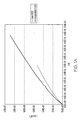
- FIG. 1A compares the experimentally observed light emission of a bare OLED and of the same OLED after coating with an integrated barrier and optical enhancement stack.
- the integrated barrier and optical enhancement stack on the OLED 100 included a 50 nm LiF plasma protective layer (RI-1.395) 105 , a 100 nm aluminum oxide barrier layer (RI-1.65) 110 , and 4 barrier stacks 115 of 0.5 ⁇ m acrylate polymer (RI-1.5) 120 and 35 nm aluminum oxide (RI-1.65) 125 .
- the graph shows the experimental I-L curves for the OLEDs.
- the I-L curve for an OLED is obtained by measuring the light emitted by the OLED device as a function of the current used for driving the device itself. The light was measured in the forward direction.
- FIG. 1A shows an enhancement of 25% for the encapsulated OLED.
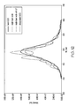
- FIG. 1B compares the experimentally observed light emission of a second bare OLED and the same OLED after encapsulation.
- the integrated barrier and optical enhancement stack included a 50 nm LiF plasma protective layer (RI-1.395), a 100 nm aluminum oxide barrier layer (RI-1.65), and 4 barrier stacks of 0.5 ⁇ m acrylate polymer (RI-1.5) and 35 nm aluminum oxide (RI-1.65).
- FIG. 1B shows the experimental I-L curves. There is an enhancement of 15% for the encapsulated OLED compared to the bare OLED.
- FIG. 1C shows the corresponding I-V curves for the bare OLED and encapsulated OLED of FIG. 2B .
- An I-V curve for an OLED is obtained by measuring the current going through the OLED while scanning the applied voltage.
- the I-V curve of the OLED before and after encapsulation overlap showing that the electrical performance of the OLED after encapsulation was not changed.
- the effect of inorganic plasma protective layers and inorganic barrier layers between the OLED and the barrier stack were evaluated using the simulation.
- the OLED has a 250 nm thick ITO cathode.
- three barrier stacks 215 are included, each having a 1 ⁇ m polymeric decoupling layer 225 and a 40 nm inorganic oxide barrier layer 230 with a 1 ⁇ m polymeric decoupling layer 220 on top of the barrier stacks 215 .
- FIG. 15 three barrier stacks 215 are included, each having a 1 ⁇ m polymeric decoupling layer 225 and a 40 nm inorganic oxide barrier layer 230 with a 1 ⁇ m polymeric decoupling layer 220 on top of the barrier stacks 215 .
- the light output of a bare OLED with a 250 nm ITO cathode was compared with encapsulated OLEDs having an inorganic plasma protective layer 205 and different thicknesses of initial inorganic barrier layers 210 (50 nm LiF/120 nm aluminum oxide; 120 nm aluminum oxide; 50 nm LiF/40 nm aluminum oxide) on the OLED 200 .
- the encapsulated OLED with the LiF inorganic plasma protective layer and 120 nm initial inorganic oxide barrier layer provided improved light output.
- the optimization was in terms of peak intensity, color purity, and color coordinates.
- the model shows that the introduction of the plasma protective layer can lead to a 20% increase in peak intensity. With a fixed electrical power input, the increase in intensity of the emitted light shows that the efficiency of the light generation has increased.
- Example 3 shows experimental results of the effect of introducing a plasma protective layer.
- FIG. 3 compares the effect of different protective layers having the same thickness.
- the graphs report experimental I-L curves. The emitted light was measured in the forward direction.
- the two OLEDs had the identical structure and had been deposited on the same motherglass (in the same run).
- the two protective layers, PL1 and PL2 had the same thickness, 50 nm.
- the RI of PL1 was 1.4
- the RI of PL2 was 1.8.
- FIG. 3A shows an enhancement of 35% for the PPL with an RI of 1.4
- FIG. 3B shows an enhancement of 14% for a PPL with the RI of 1.8.
- the light output of the OLED was optimized using the simulation by varying the cathode thickness.
- a double layered cathode including a transparent ITO layer and a semi-transparent Ag layer was used.
- the Ag layer is added to increase the conductivity of the cathode.
- the light output from the OLED having a Ag cathode and from OLEDs having different thicknesses of indium tin oxide (ITO) cathode was compared, as shown in FIG. 4 .
- the reflectivity and thickness of the cathode influence the intensity and the position of the TE-OLED emitted light.
- the OLED structure with a semitransparent Ag cathode gave the highest output intensity.
- the peak intensity of light output and the peak position depend on the thickness of the ITO layer.
- the optimum output (highest light output, and no spectral shift) was provided by a 100 nm thick ITO layer.
- the barrier structure used was 50 nm LiF/inorganic oxide barrier layer (40 nm)/3 barrier stacks (polymeric decoupling layer (Ipm)/inorganic oxide barrier layer (40 nm))/1 ⁇ m polymeric decoupling layer, and the cathode was Ag (20 nm).
- the thickness of the initial inorganic barrier layer, and the polymeric decoupling layer, and inorganic oxide barrier layer of the barrier stacks were varied.
- FIGS. 5A-5C show the effect of changing the thickness of the initial inorganic barrier layer.
- Each of the three barrier stacks had 1 ⁇ m polymeric decoupling layers, and 40 nm inorganic oxide barrier layers.
- the use of 120 nm thick initial inorganic barrier layer provided the highest peak intensity, best color purity, and minimum spectral shift. It enhances the peak intensity by 20%.
- FIGS. 6A-6E show the effect of varying the thickness of the polymeric decoupling layer in the barrier stack.
- the initial inorganic barrier layer was 120 nm thick, and the inorganic oxide barrier layer in the barrier stacks was 40 nm.
- a 1 ⁇ m polymer thickness gave the highest peak intensity, best color purity, and minimum spectral shift. The combined effects of these improvements enhances the intensity by 30%.
- FIGS. 7A-7D show the effect of different thicknesses of the inorganic oxide barrier layer in the barrier stack.
- the initial inorganic barrier layer was 120 nm thick, and the polymeric decoupling layer in the barrier stack was 1 ⁇ m.
- the 40 nm inorganic oxide barrier layer thickness provided the highest peak intensity, best color purity, and minimum spectral shift. This shows that with a fully optimized barrier and optical enhancement structure a 40% increase can be reached.
- FIGS. 8A-8B show the effect of adding layers to the OLED encapsulation structure. 50 nm LiF inorganic plasma protective layer, 120 nm initial inorganic oxide barrier layer, barrier stacks with 1 ⁇ m polymeric decoupling layer and 40 nm inorganic oxide barrier layer, and 1 ⁇ m polymeric decoupling layer were used.
- FIG. 8A shows that a substantial increase in efficiency can be obtained using the correct design rules for the barrier and optical enhancement stack. As shown in FIG. 8B , adding more barrier layers does not affect the light output.
- the two plots show how OLED encapsulation can be optimized.
- layers for protecting the OLED and good barrier performance LiF inorganic plasma protective layer and initial inorganic barrier layer for better coverage.
- the simulation in FIG. 9 shows that with the proper design of the integrated optical structure defined by an encapsulated OLED, it is possible to obtain an OLED with intentionally shifted emission, purer color, and enhanced emission.
- the cathode is 20 nm Ag
- the inorganic plasma protective layer is 50 nm LiF
- the initial inorganic oxide barrier layer is 120 nm
- the photoluminescent layer is DCJTB (4-(dicyanomethylene)-2-t-butyl-6 (1,1,7,7-tetramethyljulolidyl-9-enyl)-4 Hpyran) which has a broad orange/yellow light emission.
- the resulting encapsulated OLED has a red emission with peak intensity 1.6 times higher than the unencapsulated OLED.
- the simulation of FIG. 10 compares the light output (at 90°) for RGB OLEDs with and without encapsulation. For each color, the intensity is normalized to the output of the OLED (at 90°).
- the structure used in the encapsulation was 50 nm LiF inorganic plasma protective layer/120 nm initial inorganic oxide barrier layer/3 barrier stacks with 1 ⁇ m polymeric decoupling layer and 40 nm inorganic oxide barrier layer/1 ⁇ m polymeric decoupling layer. This structure enhanced the light output for the green and the red OLEDs.
- the intensity of the encapsulated OLED was similar to that emitted by the bare unencapsulated OLED.
- This example shows that it is possible to enhance the light output for two colors while not negatively affecting the light output of the third color.
- the overall output has been increased by 30%.
- Table 1 shows the enhancement of the structure described above with variations in the layer thicknesses as shown.
- the normalized intensity of the emission peak at 0° is reported in the table.
- the normalization is to the bare unencapsulated OLED (with no additional layers).
- the simulation in FIG. 11 compares the effect of an initial inorganic barrier layer with an initial organic layer.
- the structure contained either 120 nm initial inorganic barrier layer or 1 ⁇ m thick initial organic layer with 3 barrier stacks having 2 ⁇ m polymeric decoupling layers and 40 nm inorganic oxide barrier layers.
- the initial organic layer had an RI of 1.5.
- Example 9 shows another possible barrier layer which has a negative effect on the efficiency and spectral purity of the emission from the device.
- the simulation in FIG. 12 compares the effect of a single inorganic barrier layer with a multilayer structure.
- One sample had a 2 ⁇ m single layer of an inorganic oxide barrier layer.
- the multilayer structure included a 50 nm LiF inorganic plasma protective layer, 120 nm initial inorganic oxide barrier layer, and 3 barrier stacks with 2 ⁇ m polymeric decoupling layer and 40 nm inorganic oxide barrier layer.
- the intensity enhancement and color purity were better for the multilayer structure than for the single layer inorganic barrier layer.
- the simulation in FIG. 13 compares two OLEDs having different layer thicknesses encapsulated with the same structure.
- the intensity of the unencapsulated OLEDs was similar (+/ ⁇ about 10%), the intensity of the encapsulated OLEDs differed by about 30%.
- the barrier structure needs to optimized for the specific OLED to be used.
- the structure could be: 1) transparent substrate (e.g., glass or plastic); 2) integrated barrier and optical enhancement stack; 3) anode of OLED (e.g., ITO); 4) OLED organic emission layers; and 5) cathode of OLED (e.g., low work function metal combined with aluminum).
- transparent substrate e.g., glass or plastic
- integrated barrier and optical enhancement stack e.g., 3) anode of OLED (e.g., ITO); 4) OLED organic emission layers
- cathode of OLED e.g., low work function metal combined with aluminum
- the integrated barrier and optical enhancement stack would be adjacent to the transparent electrode in the OLED.
- the transparent electrode In a top emitting OLED structure, the transparent electrode would be the cathode, while in a bottom emitting OLED structure, the transparent electrode would be the anode.
Abstract
Description
Ē=∇(∇·
where k0=ω√{square root over (μ0∈0)}=2π/λ, wavenumber in vacuum.
and n (or ni in the ith layer) is the wavelength-dependent complex refractive index. The solution for the electrical Hertzian potential Π can be found solving the following equations:
{tilde over (Π)}(α,z)=∫0 ∞Π(ρ,z)J 0(αρ)ρd ρ
| TABLE 1 | |||||
| First Oxide | |||||
| Thickness (nm) | Alq31 | BAlq32 | DJCTB3 | ||
| 240 | 1 | 1.1 | 1.3 | ||
| 120 | 1.3 | 0.8 | 1.3 | ||
| 40 | 1.1 | 0.9 | 1.3 | ||
| Interlayer Oxide | |||||
| thickness (nm) | | BAlq3 | DJCTB | ||
| 20 | 1 | 1.1 | 1.6 | ||
| 40 | 1.2 | 0.9 | 1.3 | ||
| 60 | 1.1 | 0.8 | 1.7 | ||
| 80 | 1.1 | 1.2 | 1.4 | ||
| Interlayer Poly | |||||
| Thickness (um) | Alq3 | BAlq3 | DJCTB | ||
| 0.2 | 1 | 1.1 | 1.1 | ||
| 0.5 | 1.1 | 0.8 | 1.6 | ||
| 1 | 1.3 | 0.8 | 1.3 | ||
| 2 | 1.1 | 0.9 | 1.6 | ||
| 4 | 1.2 | 1.1 | 1.5 | ||
| 1Alq3 = aluminum tris(8-hydroxyquinoline) | |||||
| 2BAlq3 = bis(2-methyl-8-quinolinolato-N1,O8)-(1,1′-biphenyl-4-olato) aluminum | |||||
| 3DJCTB = 4-(dicyanomethylene)-2-t-butyl-6 (1,1,7,7-tetramethyljulolodyl-9-enyl)-4 Hpyran | |||||
Claims (22)
Priority Applications (1)
| Application Number | Priority Date | Filing Date | Title |
|---|---|---|---|
| US12/341,134 US9337446B2 (en) | 2008-12-22 | 2008-12-22 | Encapsulated RGB OLEDs having enhanced optical output |
Applications Claiming Priority (1)
| Application Number | Priority Date | Filing Date | Title |
|---|---|---|---|
| US12/341,134 US9337446B2 (en) | 2008-12-22 | 2008-12-22 | Encapsulated RGB OLEDs having enhanced optical output |
Publications (2)
| Publication Number | Publication Date |
|---|---|
| US20100156277A1 US20100156277A1 (en) | 2010-06-24 |
| US9337446B2 true US9337446B2 (en) | 2016-05-10 |
Family
ID=42264987
Family Applications (1)
| Application Number | Title | Priority Date | Filing Date |
|---|---|---|---|
| US12/341,134 Active 2030-03-27 US9337446B2 (en) | 2008-12-22 | 2008-12-22 | Encapsulated RGB OLEDs having enhanced optical output |
Country Status (1)
| Country | Link |
|---|---|
| US (1) | US9337446B2 (en) |
Families Citing this family (12)
| Publication number | Priority date | Publication date | Assignee | Title |
|---|---|---|---|---|
| KR101900362B1 (en) | 2012-01-16 | 2018-11-09 | 삼성디스플레이 주식회사 | Organic light emitting display apparatus and method of manufacturing organic light emitting display apparatus |
| KR20130089039A (en) | 2012-02-01 | 2013-08-09 | 삼성디스플레이 주식회사 | Deposition source, deposition apparatus and method of manufacturing organic light emitting display apparatus |
| CN103681729A (en) * | 2012-08-31 | 2014-03-26 | 群康科技(深圳)有限公司 | Organic light emitting diode panel and electronic device comprising same |
| KR101937258B1 (en) | 2012-09-04 | 2019-01-11 | 삼성디스플레이 주식회사 | Organic light emitting display apparatus |
| US9871220B2 (en) * | 2012-11-28 | 2018-01-16 | Konica Minolta, Inc. | Transparent electrode, and electronic device |
| JP6231281B2 (en) | 2013-01-23 | 2017-11-15 | 株式会社ジャパンディスプレイ | Display device |
| US9909022B2 (en) | 2014-07-25 | 2018-03-06 | Kateeva, Inc. | Organic thin film ink compositions and methods |
| WO2017039857A1 (en) | 2015-08-31 | 2017-03-09 | Kateeva, Inc. | Di- and mono(meth)acrylate based organic thin film ink compositions |
| EP3449294A1 (en) * | 2016-04-29 | 2019-03-06 | SABIC Global Technologies B.V. | High refractive index (hri) substrate and method for fabrication thereof |
| JP7144864B2 (en) | 2017-04-21 | 2022-09-30 | カティーバ, インコーポレイテッド | Compositions and techniques for forming organic thin films |
| CN107482042B (en) * | 2017-08-18 | 2020-04-03 | 京东方科技集团股份有限公司 | OLED display substrate, manufacturing method thereof and OLED display device |
| KR20220087130A (en) * | 2020-12-17 | 2022-06-24 | 한국전자통신연구원 | display device |
Citations (349)
| Publication number | Priority date | Publication date | Assignee | Title |
|---|---|---|---|---|
| US2382432A (en) | 1940-08-02 | 1945-08-14 | Crown Cork & Seal Co | Method and apparatus for depositing vaporized metal coatings |
| US2384500A (en) | 1942-07-08 | 1945-09-11 | Crown Cork & Seal Co | Apparatus and method of coating |
| BE704297A (en) | 1965-09-13 | 1968-02-01 | ||
| US3475307A (en) | 1965-02-04 | 1969-10-28 | Continental Can Co | Condensation of monomer vapors to increase polymerization rates in a glow discharge |
| US3496427A (en) | 1966-01-13 | 1970-02-17 | Gen Electric | Semiconductor device with composite encapsulation |
| US3607365A (en) | 1969-05-12 | 1971-09-21 | Minnesota Mining & Mfg | Vapor phase method of coating substrates with polymeric coating |
| US3661117A (en) | 1969-12-03 | 1972-05-09 | Stanford Research Inst | Apparatus for depositing thin lines |
| US4061835A (en) | 1975-02-27 | 1977-12-06 | Standard Oil Company (Indiana) | Process of forming a polypropylene coated substrate from an aqueous suspension of polypropylene particles |
| US4098965A (en) | 1977-01-24 | 1978-07-04 | Polaroid Corporation | Flat batteries and method of making the same |
| US4266223A (en) | 1978-12-08 | 1981-05-05 | W. H. Brady Co. | Thin panel display |
| US4283482A (en) | 1979-03-29 | 1981-08-11 | Nihon Shinku Gijutsu Kabushiki Kaisha | Dry Lithographic Process |
| US4313254A (en) | 1979-10-30 | 1982-02-02 | The Johns Hopkins University | Thin-film silicon solar cell with metal boride bottom electrode |
| US4426275A (en) | 1981-11-27 | 1984-01-17 | Deposition Technology, Inc. | Sputtering device adaptable for coating heat-sensitive substrates |
| US4521458A (en) | 1983-04-01 | 1985-06-04 | Nelson Richard C | Process for coating material with water resistant composition |
| US4537814A (en) | 1983-01-27 | 1985-08-27 | Toyoda Gosei Co., Ltd. | Resin article having a ceramics coating layer |
| US4555274A (en) | 1982-03-15 | 1985-11-26 | Fuji Photo Film Co., Ltd. | Ion selective electrode and process of preparing the same |
| US4557978A (en) | 1983-12-12 | 1985-12-10 | Primary Energy Research Corporation | Electroactive polymeric thin films |
| US4572842A (en) | 1983-09-02 | 1986-02-25 | Leybold-Heraeus Gmbh | Method and apparatus for reactive vapor deposition of compounds of metal and semi-conductors |
| US4581337A (en) | 1983-07-07 | 1986-04-08 | E. I. Du Pont De Nemours And Company | Polyether polyamines as linking agents for particle reagents useful in immunoassays |
| JPS6179644U (en) | 1984-10-27 | 1986-05-27 | ||
| US4624867A (en) | 1984-03-21 | 1986-11-25 | Nihon Shinku Gijutsu Kabushiki Kaisha | Process for forming a synthetic resin film on a substrate and apparatus therefor |
| US4695618A (en) | 1986-05-23 | 1987-09-22 | Ameron, Inc. | Solventless polyurethane spray compositions and method for applying them |
| US4710426A (en) | 1983-11-28 | 1987-12-01 | Polaroid Corporation, Patent Dept. | Solar radiation-control articles with protective overlayer |
| WO1987007848A1 (en) | 1986-06-23 | 1987-12-30 | Spectrum Control, Inc. | Flash evaporation of monomer fluids |
| US4722515A (en) | 1984-11-06 | 1988-02-02 | Spectrum Control, Inc. | Atomizing device for vaporization |
| JPS6396895U (en) | 1986-12-16 | 1988-06-22 | ||
| US4768666A (en) | 1987-05-26 | 1988-09-06 | Milton Kessler | Tamper proof container closure |
| JPS63136316U (en) | 1987-02-26 | 1988-09-07 | ||
| WO1989000337A1 (en) | 1987-06-29 | 1989-01-12 | Eastman Kodak Company | Encapsulation barrier for thick-film hybrid circuits |
| EP0299753A2 (en) | 1987-07-15 | 1989-01-18 | The BOC Group, Inc. | Controlled flow vaporizer |
| JPS6441192U (en) | 1987-09-04 | 1989-03-13 | ||
| GB2210826A (en) | 1987-10-19 | 1989-06-21 | Bowater Packaging Ltd | Microwave transparent barrier packaging materials |
| US4842893A (en) | 1983-12-19 | 1989-06-27 | Spectrum Control, Inc. | High speed process for coating substrates |
| US4855186A (en) | 1987-03-06 | 1989-08-08 | Hoechst Aktiengesellschaft | Coated plastic film and plastic laminate prepared therefrom |
| JPH0141067Y2 (en) | 1985-03-12 | 1989-12-06 | ||
| US4889609A (en) | 1988-09-06 | 1989-12-26 | Ovonic Imaging Systems, Inc. | Continuous dry etching system |
| US4913090A (en) | 1987-10-02 | 1990-04-03 | Mitsubishi Denki Kabushiki Kaisha | Chemical vapor deposition apparatus having cooling heads adjacent to gas dispersing heads in a single chamber |
| US4931158A (en) | 1988-03-22 | 1990-06-05 | The Regents Of The Univ. Of Calif. | Deposition of films onto large area substrates using modified reactive magnetron sputtering |
| US4934315A (en) | 1984-07-23 | 1990-06-19 | Alcatel N.V. | System for producing semicondutor layer structures by way of epitaxial growth |
| JPH02183230A (en) | 1989-01-09 | 1990-07-17 | Sharp Corp | Organic nonlinear optical material and production thereof |
| US4954371A (en) | 1986-06-23 | 1990-09-04 | Spectrum Control, Inc. | Flash evaporation of monomer fluids |
| US4977013A (en) | 1988-06-03 | 1990-12-11 | Andus Corporation | Tranparent conductive coatings |
| WO1991007519A1 (en) | 1989-11-08 | 1991-05-30 | The Boc Group, Inc. | Method for coating substrates with silicon based compounds |
| EP0147696B1 (en) | 1983-12-19 | 1991-07-10 | SPECTRUM CONTROL, INC. (a Pennsylvania corporation) | Miniaturized monolithic multi-layer capacitor and apparatus and method for making |
| US5032461A (en) | 1983-12-19 | 1991-07-16 | Spectrum Control, Inc. | Method of making a multi-layered article |
| US5036249A (en) | 1989-12-11 | 1991-07-30 | Molex Incorporated | Electroluminescent lamp panel and method of fabricating same |
| JPH03183759A (en) | 1989-12-12 | 1991-08-09 | Toyobo Co Ltd | Laminated plastic film and its production |
| US5059861A (en) | 1990-07-26 | 1991-10-22 | Eastman Kodak Company | Organic electroluminescent device with stabilizing cathode capping layer |
| JPH03290375A (en) | 1990-04-09 | 1991-12-20 | Sumitomo Electric Ind Ltd | Composite material reinforced with coated carbon fiber |
| EP0468440A2 (en) | 1990-07-26 | 1992-01-29 | Eastman Kodak Company | Organic electroluminescent device with stabilized cathode |
| JPH0414440Y2 (en) | 1987-06-08 | 1992-03-31 | ||
| US5124204A (en) | 1988-07-14 | 1992-06-23 | Sharp Kabushiki Kaisha | Thin film electroluminescent (EL) panel |
| JPH04267097A (en) | 1991-02-22 | 1992-09-22 | Mitsui Toatsu Chem Inc | Sealing method for organic light emitting element |
| JPH0448515Y2 (en) | 1985-09-30 | 1992-11-16 | ||
| US5189405A (en) | 1989-01-26 | 1993-02-23 | Sharp Kabushiki Kaisha | Thin film electroluminescent panel |
| US5203898A (en) | 1991-12-16 | 1993-04-20 | Corning Incorporated | Method of making fluorine/boron doped silica tubes |
| US5204314A (en) | 1990-07-06 | 1993-04-20 | Advanced Technology Materials, Inc. | Method for delivering an involatile reagent in vapor form to a CVD reactor |
| JPH05147678A (en) | 1991-11-27 | 1993-06-15 | Toyo Alum Kk | Highly moistureproof, static damage-preventive sack |
| EP0547550A1 (en) | 1991-12-16 | 1993-06-23 | Matsushita Electric Industrial Co., Ltd. | Method of manufacturing a chemically adsorbed film |
| JPH05182759A (en) | 1991-12-26 | 1993-07-23 | Pioneer Video Corp | Organic el element |
| US5237439A (en) | 1991-09-30 | 1993-08-17 | Sharp Kabushiki Kaisha | Plastic-substrate liquid crystal display device with a hard coat containing boron or a buffer layer made of titanium oxide |
| US5260095A (en) | 1992-08-21 | 1993-11-09 | Battelle Memorial Institute | Vacuum deposition and curing of liquid monomers |
| EP0590467A1 (en) | 1992-09-26 | 1994-04-06 | Röhm Gmbh | Process for forming scratch-resistant silicon oxide layers on plastics by plasma-coating |
| JPH06136159A (en) | 1992-10-27 | 1994-05-17 | Kanegafuchi Chem Ind Co Ltd | Transparent conductive film and its production |
| JPH06158305A (en) | 1992-11-27 | 1994-06-07 | Shimadzu Corp | Inline sputtering device |
| JPH06196260A (en) | 1992-09-29 | 1994-07-15 | Nec Kansai Ltd | Manufacture of electroluminescence lamp |
| EP0390540B1 (en) | 1989-03-30 | 1994-08-03 | Sharp Kabushiki Kaisha | Process for preparing an organic compound thin film for an optical device |
| US5336324A (en) | 1991-12-04 | 1994-08-09 | Emcore Corporation | Apparatus for depositing a coating on a substrate |
| JPH06223966A (en) | 1993-01-28 | 1994-08-12 | Toshiba Corp | Organic dispersion type el panel |
| EP0611037A1 (en) | 1993-01-28 | 1994-08-17 | Du Pont De Nemours International S.A. | Layered product |
| US5344501A (en) | 1992-03-23 | 1994-09-06 | Canon Kabushiki Kaisha | Solar cell |
| US5354497A (en) | 1992-04-20 | 1994-10-11 | Sharp Kabushiki Kaisha | Liquid crystal display |
| US5357063A (en) | 1993-07-12 | 1994-10-18 | Battelle Memorial Institute | Method and apparatus for acoustic energy identification of objects buried in soil |
| US5356947A (en) | 1990-03-29 | 1994-10-18 | Minnesota Mining And Manufacturing Company | Controllable radiation curable photoiniferter prepared adhesives for attachment of microelectronic devices and a method of attaching microelectronic devices therewith |
| US5376467A (en) | 1992-03-06 | 1994-12-27 | Sony Corporation | Organic electrolyte battery |
| US5393607A (en) | 1992-01-13 | 1995-02-28 | Mitsui Toatsu Chemiclas, Inc. | Laminated transparent plastic material and polymerizable monomer |
| US5402314A (en) | 1992-02-10 | 1995-03-28 | Sony Corporation | Printed circuit board having through-hole stopped with photo-curable solder resist |
| WO1995010117A1 (en) | 1993-10-04 | 1995-04-13 | Catalina Coatings, Inc. | Cross-linked acrylate coating material useful for forming capacitor dielectrics and oxygen barriers |
| JPH07147189A (en) | 1993-11-25 | 1995-06-06 | Idemitsu Kosan Co Ltd | Organic electroluminescent element |
| US5427638A (en) | 1992-06-04 | 1995-06-27 | Alliedsignal Inc. | Low temperature reaction bonding |
| JPH07192866A (en) | 1993-12-26 | 1995-07-28 | Ricoh Co Ltd | Organic thin film type electroluminescent element |
| US5440446A (en) | 1993-10-04 | 1995-08-08 | Catalina Coatings, Inc. | Acrylate coating material |
| US5451449A (en) | 1994-05-11 | 1995-09-19 | The Mearl Corporation | Colored iridescent film |
| US5461545A (en) | 1990-08-24 | 1995-10-24 | Thomson-Csf | Process and device for hermetic encapsulation of electronic components |
| US5464667A (en) | 1994-08-16 | 1995-11-07 | Minnesota Mining And Manufacturing Company | Jet plasma process and apparatus |
| JPH0872188A (en) | 1994-09-02 | 1996-03-19 | Kuraray Co Ltd | Multilayer structure and utility thereof |
| US5510173A (en) | 1993-08-20 | 1996-04-23 | Southwall Technologies Inc. | Multiple layer thin films with improved corrosion resistance |
| US5512320A (en) | 1993-01-28 | 1996-04-30 | Applied Materials, Inc. | Vacuum processing apparatus having improved throughput |
| JPH08171988A (en) | 1994-12-20 | 1996-07-02 | Showa Shell Sekiyu Kk | Electroluminescent element |
| JPH08179292A (en) | 1994-12-27 | 1996-07-12 | Dainippon Printing Co Ltd | Plastic substrate for liquid crystal display element |
| US5536323A (en) | 1990-07-06 | 1996-07-16 | Advanced Technology Materials, Inc. | Apparatus for flash vaporization delivery of reagents |
| WO1996023217A1 (en) | 1995-01-23 | 1996-08-01 | Duracell Inc. | Multilayer moisture barrier for electrochemical cell tester |
| JPH08203669A (en) | 1995-01-30 | 1996-08-09 | Seikosha Co Ltd | El double-face luminescent display body |
| US5554220A (en) | 1995-05-19 | 1996-09-10 | The Trustees Of Princeton University | Method and apparatus using organic vapor phase deposition for the growth of organic thin films with large optical non-linearities |
| US5576101A (en) | 1992-12-18 | 1996-11-19 | Bridgestone Corporation | Gas barrier rubber laminate for minimizing refrigerant leakage |
| JPH08318590A (en) | 1994-10-27 | 1996-12-03 | Carl Zeiss:Fa | Plastic container having barrier coat and manufacture thereof |
| JPH08325713A (en) | 1995-05-30 | 1996-12-10 | Matsushita Electric Works Ltd | Formation of metallic film on organic substrate surface |
| WO1997004885A1 (en) | 1995-07-27 | 1997-02-13 | Battelle Memorial Institute | Vacuum flash evaporated polymer composites |
| JPH0959763A (en) | 1995-08-25 | 1997-03-04 | Matsushita Electric Works Ltd | Formation of metallic film on surface of organic substrate |
| US5620524A (en) | 1995-02-27 | 1997-04-15 | Fan; Chiko | Apparatus for fluid delivery in chemical vapor deposition systems |
| DE19603746A1 (en) | 1995-10-20 | 1997-04-24 | Bosch Gmbh Robert | Electroluminescent layer system |
| WO1997016053A1 (en) | 1995-10-20 | 1997-05-01 | Robert Bosch Gmbh | Electroluminescent layer system |
| US5629389A (en) | 1995-06-06 | 1997-05-13 | Hewlett-Packard Company | Polymer-based electroluminescent device with improved stability |
| JPH09132774A (en) | 1995-11-10 | 1997-05-20 | Fuji Electric Co Ltd | Organic thin-film luminescent element |
| EP0777280A2 (en) | 1995-11-30 | 1997-06-04 | Motorola, Inc. | Passivation of organic devices |
| EP0777281A2 (en) | 1995-11-30 | 1997-06-04 | Motorola, Inc. | Passivation of electroluminescent organic devices |
| WO1997022631A1 (en) | 1995-12-19 | 1997-06-26 | Talison Research | Plasma deposited film networks |
| US5652192A (en) | 1992-07-10 | 1997-07-29 | Battelle Memorial Institute | Catalyst material and method of making |
| JPH09201897A (en) | 1995-11-21 | 1997-08-05 | Mitsubishi Chem Corp | Gas barrier olefin resin laminate |
| US5654084A (en) | 1994-07-22 | 1997-08-05 | Martin Marietta Energy Systems, Inc. | Protective coatings for sensitive materials |
| EP0787826A1 (en) | 1996-01-30 | 1997-08-06 | Becton, Dickinson and Company | Blood collection tube assembly |
| EP0787824A2 (en) | 1996-01-30 | 1997-08-06 | Becton, Dickinson and Company | Non-Ideal Barrier coating sequence composition |
| US5660961A (en) | 1996-01-11 | 1997-08-26 | Xerox Corporation | Electrophotographic imaging member having enhanced layer adhesion and freedom from reflection interference |
| US5665280A (en) | 1996-01-30 | 1997-09-09 | Becton Dickinson Co | Blood collection tube assembly |
| US5684084A (en) | 1995-12-21 | 1997-11-04 | E. I. Du Pont De Nemours And Company | Coating containing acrylosilane polymer to improve mar and acid etch resistance |
| US5693956A (en) | 1996-07-29 | 1997-12-02 | Motorola | Inverted oleds on hard plastic substrate |
| US5695564A (en) | 1994-08-19 | 1997-12-09 | Tokyo Electron Limited | Semiconductor processing system |
| JPH10725A (en) | 1996-06-18 | 1998-01-06 | Toppan Printing Co Ltd | Gas-barrier laminate for packaging |
| JPH1013083A (en) | 1996-06-27 | 1998-01-16 | Tosoh Corp | Electromagnetic wave absorber |
| US5711816A (en) | 1990-07-06 | 1998-01-27 | Advanced Technolgy Materials, Inc. | Source reagent liquid delivery apparatus, and chemical vapor deposition system comprising same |
| WO1998010116A1 (en) | 1996-09-05 | 1998-03-12 | Talison Research | Ultrasonic nozzle feed for plasma deposited film networks |
| US5731661A (en) | 1996-07-15 | 1998-03-24 | Motorola, Inc. | Passivation of electroluminescent organic devices |
| US5747182A (en) | 1992-07-27 | 1998-05-05 | Cambridge Display Technology Limited | Manufacture of electroluminescent devices |
| WO1998018852A1 (en) | 1996-10-31 | 1998-05-07 | Delta V Technologies, Inc. | Acrylate coating methods |
| US5759329A (en) | 1992-01-06 | 1998-06-02 | Pilot Industries, Inc. | Fluoropolymer composite tube and method of preparation |
| US5771177A (en) | 1993-05-17 | 1998-06-23 | Kyoei Automatic Control Technology Co., Ltd. | Method and apparatus for measuring dynamic load |
| US5771562A (en) | 1995-05-02 | 1998-06-30 | Motorola, Inc. | Passivation of organic devices |
| US5782355A (en) | 1994-09-30 | 1998-07-21 | Fuji Photo Film Co., Ltd. | Cassette case |
| US5792550A (en) | 1989-10-24 | 1998-08-11 | Flex Products, Inc. | Barrier film having high colorless transparency and method |
| US5795399A (en) | 1994-06-30 | 1998-08-18 | Kabushiki Kaisha Toshiba | Semiconductor device manufacturing apparatus, method for removing reaction product, and method of suppressing deposition of reaction product |
| US5811183A (en) | 1995-04-06 | 1998-09-22 | Shaw; David G. | Acrylate polymer release coated sheet materials and method of production thereof |
| US5821692A (en) | 1996-11-26 | 1998-10-13 | Motorola, Inc. | Organic electroluminescent device hermetic encapsulation package |
| JPH10312883A (en) | 1997-05-12 | 1998-11-24 | Matsushita Electric Ind Co Ltd | Organic electroluminescent element |
| US5844363A (en) | 1997-01-23 | 1998-12-01 | The Trustees Of Princeton Univ. | Vacuum deposited, non-polymeric flexible organic light emitting devices |
| US5861658A (en) | 1996-10-03 | 1999-01-19 | International Business Machines Corporation | Inorganic seal for encapsulation of an organic layer and method for making the same |
| US5869791A (en) | 1995-04-18 | 1999-02-09 | U.S. Philips Corporation | Method and apparatus for a touch sensing device having a thin film insulation layer about the periphery of each sensing element |
| JPH1140344A (en) | 1997-07-16 | 1999-02-12 | Casio Comput Co Ltd | Electroluminescent element |
| US5872355A (en) | 1997-04-09 | 1999-02-16 | Hewlett-Packard Company | Electroluminescent device and fabrication method for a light detection system |
| US5891554A (en) | 1994-02-25 | 1999-04-06 | Idemitsu Kosan Co., Ltd. | Organic electroluminescence device |
| WO1999016931A1 (en) | 1997-09-29 | 1999-04-08 | Battelle Memorial Institute | Plasma enhanced chemical deposition with low vapor pressure compounds |
| WO1999016557A1 (en) | 1997-09-29 | 1999-04-08 | Battelle Memorial Institute | Flash evaporation of liquid monomer particle mixture |
| US5895228A (en) | 1996-11-14 | 1999-04-20 | International Business Machines Corporation | Encapsulation of organic light emitting devices using Siloxane or Siloxane derivatives |
| US5902688A (en) | 1996-07-16 | 1999-05-11 | Hewlett-Packard Company | Electroluminescent display device |
| EP0915105A1 (en) | 1997-11-07 | 1999-05-12 | Rohm And Haas Company | Plastic substrates for electronic display applications |
| US5904958A (en) | 1998-03-20 | 1999-05-18 | Rexam Industries Corp. | Adjustable nozzle for evaporation or organic monomers |
| EP0916394A2 (en) | 1997-11-14 | 1999-05-19 | Sharp Kabushiki Kaisha | Method of manufacturing modified particles and manufacturing device therefor |
| JPH11149826A (en) | 1997-11-17 | 1999-06-02 | Sumitomo Bakelite Co Ltd | Conductive film |
| US5912069A (en) | 1996-12-19 | 1999-06-15 | Sigma Laboratories Of Arizona | Metal nanolaminate composite |
| US5919328A (en) | 1996-01-30 | 1999-07-06 | Becton Dickinson And Company | Blood collection tube assembly |
| US5920080A (en) | 1997-06-23 | 1999-07-06 | Fed Corporation | Emissive display using organic light emitting diodes |
| WO1999033651A1 (en) | 1997-12-31 | 1999-07-08 | Kimberly-Clark Worldwide, Inc. | Microlayer breathable films of degradable polymers and thermoplastic elastomers |
| US5922161A (en) | 1995-06-30 | 1999-07-13 | Commonwealth Scientific And Industrial Research Organisation | Surface treatment of polymers |
| US5929562A (en) | 1995-04-18 | 1999-07-27 | Cambridge Display Technology Limited | Organic light-emitting devices |
| EP0931850A1 (en) | 1998-01-26 | 1999-07-28 | Leybold Systems GmbH | Method for treating the surfaces of plastic substrates |
| US5934856A (en) | 1994-05-23 | 1999-08-10 | Tokyo Electron Limited | Multi-chamber treatment system |
| US5948552A (en) | 1996-08-27 | 1999-09-07 | Hewlett-Packard Company | Heat-resistant organic electroluminescent device |
| US5952778A (en) | 1997-03-18 | 1999-09-14 | International Business Machines Corporation | Encapsulated organic light emitting device |
| WO1999046120A1 (en) | 1998-03-12 | 1999-09-16 | E.I. Du Pont De Nemours And Company | Oxygen barrier composite film structure |
| US5965907A (en) | 1997-09-29 | 1999-10-12 | Motorola, Inc. | Full color organic light emitting backlight device for liquid crystal display applications |
| US5968620A (en) | 1996-01-30 | 1999-10-19 | Becton Dickinson And Company | Blood collection tube assembly |
| US5994174A (en) | 1997-09-29 | 1999-11-30 | The Regents Of The University Of California | Method of fabrication of display pixels driven by silicon thin film transistors |
| US5996498A (en) | 1998-03-12 | 1999-12-07 | Presstek, Inc. | Method of lithographic imaging with reduced debris-generated performance degradation and related constructions |
| US6013337A (en) | 1996-01-30 | 2000-01-11 | Becton Dickinson And Company | Blood collection tube assembly |
| EP0977469A2 (en) | 1998-07-30 | 2000-02-02 | Hewlett-Packard Company | Improved transparent, flexible permeability barrier for organic electroluminescent devices |
| US6040017A (en) | 1998-10-02 | 2000-03-21 | Sigma Laboratories, Inc. | Formation of multilayered photonic polymer composites |
| US6045864A (en) | 1997-12-01 | 2000-04-04 | 3M Innovative Properties Company | Vapor coating method |
| CA2353506A1 (en) | 1998-11-02 | 2000-05-11 | 3M Innovative Properties Company | Transparent conductive oxides for plastic flat panel displays |
| US6066826A (en) | 1998-03-16 | 2000-05-23 | Yializis; Angelo | Apparatus for plasma treatment of moving webs |
| WO2000035993A1 (en) | 1998-12-18 | 2000-06-22 | The Regents Of The University Of California | Methods, compositions, and biomimetic catalysts for in vitro synthesis of silica, polysilsequioxane, polysiloxane, and polymetallo-oxanes |
| WO2000035603A1 (en) | 1998-12-16 | 2000-06-22 | Battelle Memorial Institute | Plasma enhanced chemical deposition for high and/or low index of refraction polymers |
| WO2000035604A1 (en) | 1998-12-16 | 2000-06-22 | Battelle Memorial Institute | Plasma enhanced polymer deposition onto fixtures |
| WO2000036665A1 (en) | 1998-12-16 | 2000-06-22 | Battelle Memorial Institute | Environmental barrier material for organic light emitting device and method of making |
| WO2000036661A1 (en) | 1998-12-17 | 2000-06-22 | Cambridge Display Technology Ltd. | Organic light-emitting devices |
| US6083313A (en) | 1999-07-27 | 2000-07-04 | Advanced Refractory Technologies, Inc. | Hardcoats for flat panel display substrates |
| US6084702A (en) | 1998-10-15 | 2000-07-04 | Pleotint, L.L.C. | Thermochromic devices |
| US6083628A (en) | 1994-11-04 | 2000-07-04 | Sigma Laboratories Of Arizona, Inc. | Hybrid polymer film |
| US6087007A (en) | 1994-09-30 | 2000-07-11 | Kanegafuchi Kagaku Kogyo Kabushiki Kaisha | Heat-Resistant optical plastic laminated sheet and its producing method |
| EP1021070A1 (en) | 1999-01-14 | 2000-07-19 | TDK Corporation | Organic electroluminescent device |
| US6092269A (en) | 1996-04-04 | 2000-07-25 | Sigma Laboratories Of Arizona, Inc. | High energy density capacitor |
| US6106627A (en) | 1996-04-04 | 2000-08-22 | Sigma Laboratories Of Arizona, Inc. | Apparatus for producing metal coated polymers |
| US6118218A (en) | 1999-02-01 | 2000-09-12 | Sigma Technologies International, Inc. | Steady-state glow-discharge plasma at atmospheric pressure |
| US6117266A (en) | 1997-12-19 | 2000-09-12 | Interuniversifair Micro-Elektronica Cenirum (Imec Vzw) | Furnace for continuous, high throughput diffusion processes from various diffusion sources |
| US6146462A (en) | 1998-05-08 | 2000-11-14 | Astenjohnson, Inc. | Structures and components thereof having a desired surface characteristic together with methods and apparatuses for producing the same |
| US6150187A (en) | 1997-11-20 | 2000-11-21 | Electronics And Telecommunications Research Institute | Encapsulation method of a polymer or organic light emitting device |
| US6178082B1 (en) | 1998-02-26 | 2001-01-23 | International Business Machines Corporation | High temperature, conductive thin film diffusion barrier for ceramic/metal systems |
| US6195142B1 (en) | 1995-12-28 | 2001-02-27 | Matsushita Electrical Industrial Company, Ltd. | Organic electroluminescence element, its manufacturing method, and display device using organic electroluminescence element |
| US6198220B1 (en) | 1997-07-11 | 2001-03-06 | Emagin Corporation | Sealing structure for organic light emitting devices |
| US6203898B1 (en) | 1997-08-29 | 2001-03-20 | 3M Innovatave Properties Company | Article comprising a substrate having a silicone coating |
| US6207239B1 (en) | 1998-12-16 | 2001-03-27 | Battelle Memorial Institute | Plasma enhanced chemical deposition of conjugated polymer |
| US6228436B1 (en) | 1998-12-16 | 2001-05-08 | Battelle Memorial Institute | Method of making light emitting polymer composite material |
| US6228434B1 (en) | 1998-12-16 | 2001-05-08 | Battelle Memorial Institute | Method of making a conformal coating of a microtextured surface |
| US6264747B1 (en) | 1995-03-20 | 2001-07-24 | 3M Innovative Properties Company | Apparatus for forming multicolor interference coating |
| US6268695B1 (en) | 1998-12-16 | 2001-07-31 | Battelle Memorial Institute | Environmental barrier material for organic light emitting device and method of making |
| US6274204B1 (en) | 1998-12-16 | 2001-08-14 | Battelle Memorial Institute | Method of making non-linear optical polymer |
| US20010015074A1 (en) | 1999-11-03 | 2001-08-23 | Applied Materials, Inc. | Consecutive deposition system |
| EP1130420A2 (en) | 1999-12-27 | 2001-09-05 | Nitto Denko Corporation | Transparent laminate, method for producing the same, and plasma display panel |
| WO2001068360A1 (en) | 2000-03-15 | 2001-09-20 | Cpfilms, Inc. | Flame retardant optical films |
| WO2001082389A1 (en) | 2000-04-20 | 2001-11-01 | Battelle Memorial Institute | Encapsulated display device |
| WO2001081649A1 (en) | 2000-04-20 | 2001-11-01 | Battelle Memorial Institute | Barrier coating |
| WO2001082336A2 (en) | 2000-04-20 | 2001-11-01 | Battelle Memorial Institute | Laminate comprising barrier layers on a substrate |
| WO2001087825A1 (en) | 2000-04-04 | 2001-11-22 | The Regents Of The University Of California | Methods, compositions and bi-functional catalysts for synthesis of silica, glass, silicones |
| WO2001089006A1 (en) | 2000-05-15 | 2001-11-22 | Battelle Memorial Institute | Encapsulated microelectronic devices |
| US6322860B1 (en) | 1998-11-02 | 2001-11-27 | Rohm And Haas Company | Plastic substrates for electronic display applications |
| US6333065B1 (en) | 1997-07-25 | 2001-12-25 | Tdk Corporation | Process for the production of an organic electroluminescent device |
| US6350034B1 (en) | 1999-02-26 | 2002-02-26 | 3M Innovative Properties Company | Retroreflective articles having polymer multilayer reflective coatings |
| US20020025444A1 (en) | 1998-01-13 | 2002-02-28 | 3M Innovative Properties Company | Multilayered polymer films with recyclable or recycled layers |
| US6352777B1 (en) | 1998-08-19 | 2002-03-05 | The Trustees Of Princeton University | Organic photosensitive optoelectronic devices with transparent electrodes |
| US6358570B1 (en) | 1999-03-31 | 2002-03-19 | Battelle Memorial Institute | Vacuum deposition and curing of oligomers and resins |
| US6361885B1 (en) | 1998-04-10 | 2002-03-26 | Organic Display Technology | Organic electroluminescent materials and device made from such materials |
| WO2002026973A1 (en) | 2000-09-07 | 2002-04-04 | Biowindow Gene Development Inc. Shanghai | A novel polypeptide-human heterogeneous nuclear ribonucleoprotein 32.01 and the polynucleotide encoding said polypeptide |
| JP2002151254A (en) | 2000-11-09 | 2002-05-24 | Denso Corp | Manufacturing method of organic el element |
| US6397776B1 (en) | 2001-06-11 | 2002-06-04 | General Electric Company | Apparatus for large area chemical vapor deposition using multiple expanding thermal plasma generators |
| US20020068143A1 (en) | 2000-12-01 | 2002-06-06 | Silvernail Jeffrey Alan | Adhesive sealed organic optoelectronic structures |
| US20020069826A1 (en) | 2000-09-15 | 2002-06-13 | Shipley Company, L.L.C. | Continuous feed coater |
| WO2002051626A1 (en) | 2000-12-22 | 2002-07-04 | Avery Dennison Corporation | Three-dimensional flexible adhesive film structures |
| US6416872B1 (en) | 2000-08-30 | 2002-07-09 | Cp Films, Inc. | Heat reflecting film with low visible reflectance |
| US20020096114A1 (en) | 2001-01-22 | 2002-07-25 | Applied Materials, Inc. | Series chamber for substrate processing |
| US20020102818A1 (en) | 2000-08-31 | 2002-08-01 | Sandhu Gurtej S. | Deposition methods and apparatuses providing surface activation |
| US6436544B1 (en) | 1997-07-17 | 2002-08-20 | Toray Plastics Europe S.A. | Composite metal-coated polyester films with barrier properties |
| WO2002071506A1 (en) | 2001-02-15 | 2002-09-12 | Emagin Corporation | Thin film encapsulation of organic light emitting diode devices |
| US20020140347A1 (en) | 2001-03-29 | 2002-10-03 | Weaver Michael Stuart | Methods and structures for reducing lateral diffusion through cooperative barrier layers |
| US20020139303A1 (en) | 2001-02-01 | 2002-10-03 | Shunpei Yamazaki | Deposition apparatus and deposition method |
| US6465953B1 (en) | 2000-06-12 | 2002-10-15 | General Electric Company | Plastic substrates with improved barrier properties for devices sensitive to water and/or oxygen, such as organic electroluminescent devices |
| US6468595B1 (en) | 2001-02-13 | 2002-10-22 | Sigma Technologies International, Inc. | Vaccum deposition of cationic polymer systems |
| US6469437B1 (en) | 1997-11-03 | 2002-10-22 | The Trustees Of Princeton University | Highly transparent organic light emitting device employing a non-metallic cathode |
| US6469438B2 (en) * | 1999-04-05 | 2002-10-22 | Idemitsu Kosan Co., Ltd. | Organic electroluminescence device with prescribed optical path length |
| EP1278244A2 (en) | 2001-07-20 | 2003-01-22 | Lg Electronics Inc. | Panel display device and method for forming protective layer within the same |
| US6512561B1 (en) | 1997-08-29 | 2003-01-28 | Sharp Kabushiki Kaisha | Liquid crystal display with at least one phase compensation element |
| US20030038590A1 (en) | 2001-08-21 | 2003-02-27 | Silvernail Jeffrey Alan | Patterned oxygen and moisture absorber for organic optoelectronic device structures |
| WO2003016589A1 (en) | 2001-08-20 | 2003-02-27 | Nova-Plasma Inc. | Coatings with low permeation of gases and vapors |
| US20030085652A1 (en) | 2001-11-06 | 2003-05-08 | Weaver Michael Stuart | Encapsulation structure that acts as a multilayer mirror |
| US6570714B2 (en) | 2000-02-16 | 2003-05-27 | Zms, Llc | Precision composite article |
| US20030098647A1 (en) | 2001-11-27 | 2003-05-29 | Silvernail Jeffrey Alan | Protected organic optoelectronic devices |
| US6576351B2 (en) | 2001-02-16 | 2003-06-10 | Universal Display Corporation | Barrier region for optoelectronic devices |
| US20030127973A1 (en) | 2002-01-10 | 2003-07-10 | Weaver Michael Stuart | OLEDs having increased external electroluminescence quantum efficiencies |
| US6592969B1 (en) | 1998-04-02 | 2003-07-15 | Cambridge Display Technology Limited | Flexible substrates for organic devices |
| US6614057B2 (en) | 2001-02-07 | 2003-09-02 | Universal Display Corporation | Sealed organic optoelectronic structures |
| US6624568B2 (en) | 2001-03-28 | 2003-09-23 | Universal Display Corporation | Multilayer barrier region containing moisture- and oxygen-absorbing material for optoelectronic devices |
| US6628071B1 (en) | 2002-09-03 | 2003-09-30 | Au Optronics Corporation | Package for organic electroluminescent device |
| US20030184222A1 (en) | 1998-08-03 | 2003-10-02 | Boo Nilsson | Encapsulation of polymer based solid state devices with inorganic materials |
| JP2003282239A (en) | 2002-03-25 | 2003-10-03 | Pioneer Electronic Corp | Organic electroluminescence display panel and its manufacturing method |
| US20030197197A1 (en) | 2002-04-12 | 2003-10-23 | Brown Julia J. | Organic electronic devices with pressure sensitive adhesive layer |
| US20030203210A1 (en) | 2002-04-30 | 2003-10-30 | Vitex Systems, Inc. | Barrier coatings and methods of making same |
| US20030205845A1 (en) | 2002-05-02 | 2003-11-06 | Karl Pichler | Encapsulation for organic light emitting diodes devices |
| US6653780B2 (en) | 2001-05-11 | 2003-11-25 | Pioneer Corporation | Luminescent display device and method of manufacturing same |
| WO2003098716A1 (en) | 2002-05-21 | 2003-11-27 | Otb Group B.V. | Method for manufacturing a polymer oled |
| US20030218422A1 (en) | 2002-05-23 | 2003-11-27 | Samsung Sdi Co., Ltd. | Method for encapsulating organic electroluminescent device and an organic electroluminescent panel using the same |
| US20040002729A1 (en) | 1996-10-08 | 2004-01-01 | Zamore Alan M. | Irradiation conversion of thermoplastic to thermoset polymers |
| US6681716B2 (en) | 2001-11-27 | 2004-01-27 | General Electric Company | Apparatus and method for depositing large area coatings on non-planar surfaces |
| US20040018305A1 (en) | 2002-04-15 | 2004-01-29 | Pagano John Chris | Apparatus for depositing a multilayer coating on discrete sheets |
| US20040029334A1 (en) | 2002-05-21 | 2004-02-12 | Otb Group B.V. | Method for passivating a semiconductor substrate |
| US20040031442A1 (en) | 2002-05-17 | 2004-02-19 | Semiconductor Energy Laboratory Co., Ltd. | Evaporation method, evaporation device and method of fabricating light emitting device |
| WO2004016992A1 (en) | 2002-07-18 | 2004-02-26 | Sumitomo Precision Products Co., Ltd. | Gas humidifier |
| WO2004006199A3 (en) | 2002-07-08 | 2004-03-04 | Abb Patent Gmbh | Method for monitoring a flow meter |
| US6703780B2 (en) | 2001-01-16 | 2004-03-09 | General Electric Company | Organic electroluminescent device with a ceramic output coupler and method of making the same |
| US20040046497A1 (en) | 2002-09-11 | 2004-03-11 | General Electric Company | Diffusion barrier coatings having graded compositions and devices incorporating the same |
| US6710542B2 (en) | 2002-08-03 | 2004-03-23 | Agilent Technologies, Inc. | Organic light emitting device with improved moisture seal |
| US20040071971A1 (en) | 2002-10-11 | 2004-04-15 | General Electric Company | Bond layer for coatings on plastic substrates |
| US6734625B2 (en) | 2002-07-30 | 2004-05-11 | Xerox Corporation | Organic light emitting device (OLED) with multiple capping layers passivation region on an electrode |
| US6737753B2 (en) | 2001-09-28 | 2004-05-18 | Osram Opto Semiconductor Gmbh | Barrier stack |
| US6743524B2 (en) | 2002-05-23 | 2004-06-01 | General Electric Company | Barrier layer for an article and method of making said barrier layer by expanding thermal plasma |
| US6749940B1 (en) | 1999-05-07 | 2004-06-15 | Kureha Chemical Industry Co., Ltd. | Moistureproof multilayered film |
| US20040115859A1 (en) | 2002-10-21 | 2004-06-17 | Kohji Murayama | Organic electroluminescent device and display apparatus |
| US20040113542A1 (en) | 2002-12-11 | 2004-06-17 | Applied Materials, Inc. | Low temperature process for passivation applications |
| JP2004176111A (en) | 2002-11-26 | 2004-06-24 | Matsushita Electric Ind Co Ltd | Method and apparatus for forming resin vapor-deposition film |
| US20040119028A1 (en) | 2002-12-19 | 2004-06-24 | 3M Innovative Properties Company | Laser patterning of encapsulated organic light emitting diodes |
| US6765351B2 (en) | 2001-12-20 | 2004-07-20 | The Trustees Of Princeton University | Organic optoelectronic device structures |
| US6777871B2 (en) | 2000-03-31 | 2004-08-17 | General Electric Company | Organic electroluminescent devices with enhanced light extraction |
| WO2004070840A1 (en) | 2002-12-24 | 2004-08-19 | Otb Group B.V. | Method for manufacturing an organic electroluminescent display device, substrate to be used with such a method and an organic electroluminescent display device obtained with the method |
| US20040187999A1 (en) | 2002-12-27 | 2004-09-30 | Wilkinson Matthew C. | Method for encapsulation of light emitting polymer devices and apparatus made by same |
| US6803245B2 (en) | 2001-09-28 | 2004-10-12 | Osram Opto Semiconductors Gmbh | Procedure for encapsulation of electronic devices |
| WO2004089620A2 (en) | 2003-04-02 | 2004-10-21 | 3M Innovative Properties Company | Flexible high-temperature ultrabarrier |
| US20040209090A1 (en) | 2003-01-20 | 2004-10-21 | Fuji Photo Film Co., Ltd. | Gas barrier laminate film and method for producing same |
| JP2004294601A (en) | 2003-03-26 | 2004-10-21 | Nitto Denko Corp | Anti-reflection film, optical element, and image display device |
| US20040212759A1 (en) | 2003-03-27 | 2004-10-28 | Seiko Epson Corporation | Electro-optical device, method of manufacturing the same, and electronic apparatus |
| JP2004309932A (en) | 2003-04-09 | 2004-11-04 | Dainippon Printing Co Ltd | Base material for display element, display panel, display device and method for manufacturing base material for display element |
| US20040219380A1 (en) | 2003-03-31 | 2004-11-04 | Fuji Photo Film Co., Ltd. | Gas barrier laminate film and production method therefor as well as substrate and image display device utilizing the film |
| US6815887B2 (en) | 2001-12-26 | 2004-11-09 | Samsung Sdi Co., Ltd. | Organic electroluminescent display device |
| US6818291B2 (en) | 2002-08-17 | 2004-11-16 | 3M Innovative Properties Company | Durable transparent EMI shielding film |
| US20040229051A1 (en) | 2003-05-15 | 2004-11-18 | General Electric Company | Multilayer coating package on flexible substrates for electro-optical devices |
| US6822391B2 (en) | 2001-02-21 | 2004-11-23 | Semiconductor Energy Laboratory Co., Ltd. | Light emitting device, electronic equipment, and method of manufacturing thereof |
| US20040241454A1 (en) | 1993-10-04 | 2004-12-02 | Shaw David G. | Barrier sheet and method of making same |
| US6827788B2 (en) | 2000-12-27 | 2004-12-07 | Anelva Corporation | Substrate processing device and through-chamber |
| WO2004112165A1 (en) | 2003-06-16 | 2004-12-23 | Koninklijke Philips Electronics N.V. | Barrier laminate for an electroluminescent device |
| US6836070B2 (en) | 2001-10-17 | 2004-12-28 | Chi Mei Optoelectronics Corporation | Organic electro-luminescent display and method of sealing the same |
| US20040263038A1 (en) | 2003-06-24 | 2004-12-30 | Augusto Ribolzi | Domestic refrigeration appliance with removable shelf supports |
| US6837950B1 (en) | 1998-11-05 | 2005-01-04 | Interface, Inc. | Separation of floor covering components for recycling |
| US20050006786A1 (en) | 2002-03-01 | 2005-01-13 | Kabushiki Kaisha Toshiba | Semiconductor device and method of fabricating the same |
| US6852356B2 (en) | 2002-03-01 | 2005-02-08 | Sanyo Electric Co., Ltd. | Evaporation method and manufacturing method of display device |
| WO2005015655A1 (en) | 2003-08-12 | 2005-02-17 | Otb Group B.V. | Method for applying a thin film barrier stack to a device with microstructures, and device provided with such a thin film barrier stack |
| US6864629B2 (en) | 1999-01-29 | 2005-03-08 | Pioneer Corporation | Organic electroluminescence (EL) cell that prevents moisture from deteriorating light-emitting characteristics and a method for producing the same |
| US20050051094A1 (en) | 2003-09-05 | 2005-03-10 | Mark Schaepkens | Replaceable plate expanded thermal plasma apparatus and method |
| US6866901B2 (en) | 1999-10-25 | 2005-03-15 | Vitex Systems, Inc. | Method for edge sealing barrier films |
| US6867539B1 (en) | 2000-07-12 | 2005-03-15 | 3M Innovative Properties Company | Encapsulated organic electronic devices and method for making same |
| US6872248B2 (en) | 2002-03-29 | 2005-03-29 | Canon Kabushiki Kaisha | Liquid-phase growth process and liquid-phase growth apparatus |
| US6878467B2 (en) | 2001-04-10 | 2005-04-12 | Chi Mei Optoelectronics Corporation | Organic electro-luminescence element used in a display device |
| US20050079380A1 (en) | 2003-09-30 | 2005-04-14 | Fuji Photo Film Co., Ltd. | Gas barrier laminate film and method for producing the same |
| US20050079295A1 (en) | 2001-11-27 | 2005-04-14 | Marc Schaepkens | Apparatus and method for depositing large area coatings on planar surfaces |
| US20050095736A1 (en) | 2003-11-04 | 2005-05-05 | Raghunath Padiyath | Method of making an organic light emitting device |
| US20050094394A1 (en) | 2003-11-04 | 2005-05-05 | 3M Innovative Properties Company | Segmented organic light emitting device |
| US20050093001A1 (en) | 2003-10-30 | 2005-05-05 | General Electric Company | Organic electro-optic device and method for making the same |
| US20050093437A1 (en) | 2003-10-31 | 2005-05-05 | Ouyang Michael X. | OLED structures with strain relief, antireflection and barrier layers |
| US20050095422A1 (en) | 2003-10-31 | 2005-05-05 | Nanosolar, Inc. | Inorganic/organic hybrid nanolaminate barrier film |
| US6891330B2 (en) | 2002-03-29 | 2005-05-10 | General Electric Company | Mechanically flexible organic electroluminescent device with directional light emission |
| US6897607B2 (en) | 2000-09-25 | 2005-05-24 | Pioneer Corporation | Organic electroluminescent display panel having an inorganic barrier film |
| US6897474B2 (en) | 2002-04-12 | 2005-05-24 | Universal Display Corporation | Protected organic electronic devices and methods for making the same |
| US20050112378A1 (en) | 2003-09-30 | 2005-05-26 | Fuji Photo Film Co., Ltd. | Gas barrier film and method for producing the same |
| US6902905B2 (en) | 1999-04-22 | 2005-06-07 | Cygnus, Inc. | Glucose measuring assembly with a hydrogel |
| US20050122039A1 (en) | 2002-03-13 | 2005-06-09 | Matsushita Electric Industrial Co., Ltd. | Organic luminescence device and its production method |
| US6905769B2 (en) | 2001-06-08 | 2005-06-14 | Dai Nippon Priting Co., Ltd. | Gas barrier film |
| US20050133781A1 (en) | 2003-12-19 | 2005-06-23 | General Electric Company | Multilayer device and method of making |
| US20050140291A1 (en) | 2003-12-26 | 2005-06-30 | Yoshiharu Hirakata | Light emitting device, electronic appliance, and method for manufacturing light emitting device |
| US20050146267A1 (en) | 2002-04-04 | 2005-07-07 | Dielectric Systems, Inc. | Organic light emitting device having a protective barrier |
| US20050174045A1 (en) | 2002-04-04 | 2005-08-11 | Dielectric Systems, Inc. | Organic light-emitting device display having a plurality of passive polymer layers |
| US6936131B2 (en) | 2002-01-31 | 2005-08-30 | 3M Innovative Properties Company | Encapsulation of organic electronic devices using adsorbent loaded adhesives |
| US20050212419A1 (en) | 2004-03-23 | 2005-09-29 | Eastman Kodak Company | Encapsulating oled devices |
| US20050224935A1 (en) | 2004-04-02 | 2005-10-13 | Marc Schaepkens | Organic electronic packages having hermetically sealed edges and methods of manufacturing such packages |
| US20050239294A1 (en) | 2002-04-15 | 2005-10-27 | Rosenblum Martin P | Apparatus for depositing a multilayer coating on discrete sheets |
| US20050238846A1 (en) | 2004-03-10 | 2005-10-27 | Fuji Photo Film Co., Ltd. | Gas barrier laminate film, method for producing the same and image display device utilizing the film |
| US6975067B2 (en) | 2002-12-19 | 2005-12-13 | 3M Innovative Properties Company | Organic electroluminescent device and encapsulation method |
| US20060003474A1 (en) | 2004-06-30 | 2006-01-05 | Eastman Kodak Company | Roll-to-sheet manufacture of OLED materials |
| US20060028128A1 (en) | 2004-03-08 | 2006-02-09 | Fuji Photo Film Co., Ltd. | Display device |
| US6998648B2 (en) | 2003-08-25 | 2006-02-14 | Universal Display Corporation | Protected organic electronic device structures incorporating pressure sensitive adhesive and desiccant |
| US20060063015A1 (en) | 2004-09-23 | 2006-03-23 | 3M Innovative Properties Company | Protected polymeric film |
| US20060061272A1 (en) | 2004-09-23 | 2006-03-23 | 3M Innovative Properties Company | Organic electroluminescent device |
| US7029765B2 (en) | 2003-04-22 | 2006-04-18 | Universal Display Corporation | Organic light emitting devices having reduced pixel shrinkage |
| DE102004063619A1 (en) | 2004-12-27 | 2006-07-06 | Cfs Kempten Gmbh | Shrinkable multilayer film with a release layer |
| WO2006093898A1 (en) | 2005-03-01 | 2006-09-08 | Milprint, Inc. | Multilayer packaging with peelable coupon |
| US7112351B2 (en) | 2002-02-26 | 2006-09-26 | Sion Power Corporation | Methods and apparatus for vacuum thin film deposition |
| US20060216951A1 (en) | 2003-04-11 | 2006-09-28 | Lorenza Moro | Method of making an encapsulated sensitive device |
| US20060246811A1 (en) | 2005-04-28 | 2006-11-02 | Eastman Kodak Company | Encapsulating emissive portions of an OLED device |
| EP1719808A2 (en) | 2005-05-06 | 2006-11-08 | Eastman Chemical Company | Pressure sensitive adhesive laminates |
| US20060250084A1 (en) | 2005-05-04 | 2006-11-09 | Eastman Kodak Company | OLED device with improved light output |
| US20070009674A1 (en) | 2003-05-29 | 2007-01-11 | Yasushi Okubo | Transparent film for display substrate, display substrate using the film and method of manufacturing the same, liquid crystal display, organic electroluminescence display, and touch panel |
| US7166007B2 (en) | 1999-12-17 | 2007-01-23 | Osram Opto Semiconductors Gmbh | Encapsulation of electronic devices |
| US20070033965A1 (en) | 2005-08-09 | 2007-02-15 | Carrier Corporation | Refrigerant system with suction line restrictor for capacity correction |
| US20070049155A1 (en) | 2005-08-25 | 2007-03-01 | Vitex Systems, Inc. | Encapsulated devices and method of making |
| US7198832B2 (en) | 1999-10-25 | 2007-04-03 | Vitex Systems, Inc. | Method for edge sealing barrier films |
| US7221093B2 (en) | 2002-06-10 | 2007-05-22 | Institute Of Materials Research And Engineering | Patterning of electrodes in OLED devices |
| US7255823B1 (en) | 2000-09-06 | 2007-08-14 | Institute Of Materials Research And Engineering | Encapsulation for oled devices |
| US20070187759A1 (en) | 2006-02-14 | 2007-08-16 | Samsung Electronics Co., Ltd. | Display apparatus and fabricating method thereof |
| EP1857270A1 (en) | 2006-05-17 | 2007-11-21 | Curwood, Inc. | Myoglobin blooming agent, films, packages and methods for packaging |
| WO2008097297A2 (en) | 2007-02-06 | 2008-08-14 | Sion Power Corporation | Co-flash evaporation of polymerizable monomers and non-polymerizable carrier solvent/salt mixtures/solutions |
| JP2008275737A (en) | 2007-04-26 | 2008-11-13 | Toppan Printing Co Ltd | Optical thin film layered product |
| WO2008144080A1 (en) | 2007-05-18 | 2008-11-27 | Henkel Ag & Co. Kgaa | Organic electronic devices protected by elastomeric laminating adhesive |
| US20090258235A1 (en) | 2008-04-14 | 2009-10-15 | Tomomi Tateishi | Barrier laminate, barrier film substrate and device |
| US7621794B2 (en) | 2005-11-09 | 2009-11-24 | International Display Systems, Inc. | Method of encapsulating an organic light-emitting device |
| JP5290972B2 (en) | 2006-08-10 | 2013-09-18 | メルク パテント ゲゼルシャフト ミット ベシュレンクテル ハフツング | 2- (Heterocyclylbenzyl) pyridazinone derivatives |
| JP5501587B2 (en) | 2007-09-28 | 2014-05-21 | 株式会社船井電機新応用技術研究所 | Electrochromic display device |
Family Cites Families (2)
| Publication number | Priority date | Publication date | Assignee | Title |
|---|---|---|---|---|
| DE3324106A1 (en) * | 1983-07-05 | 1985-01-17 | Draiswerke Gmbh, 6800 Mannheim | METHOD FOR GLUING WOOD CHIPS AND THE LIKE WITH LIQUID GLUE AND DEVICE FOR CARRYING OUT THE METHOD |
| DE19817777C1 (en) * | 1998-04-21 | 1999-09-09 | Schmalz J Gmbh | Suction handling head for flat panels |
-
2008
- 2008-12-22 US US12/341,134 patent/US9337446B2/en active Active
Patent Citations (435)
| Publication number | Priority date | Publication date | Assignee | Title |
|---|---|---|---|---|
| US2382432A (en) | 1940-08-02 | 1945-08-14 | Crown Cork & Seal Co | Method and apparatus for depositing vaporized metal coatings |
| US2384500A (en) | 1942-07-08 | 1945-09-11 | Crown Cork & Seal Co | Apparatus and method of coating |
| US3475307A (en) | 1965-02-04 | 1969-10-28 | Continental Can Co | Condensation of monomer vapors to increase polymerization rates in a glow discharge |
| BE704297A (en) | 1965-09-13 | 1968-02-01 | ||
| US3496427A (en) | 1966-01-13 | 1970-02-17 | Gen Electric | Semiconductor device with composite encapsulation |
| US3607365A (en) | 1969-05-12 | 1971-09-21 | Minnesota Mining & Mfg | Vapor phase method of coating substrates with polymeric coating |
| US3661117A (en) | 1969-12-03 | 1972-05-09 | Stanford Research Inst | Apparatus for depositing thin lines |
| US4061835A (en) | 1975-02-27 | 1977-12-06 | Standard Oil Company (Indiana) | Process of forming a polypropylene coated substrate from an aqueous suspension of polypropylene particles |
| US4098965A (en) | 1977-01-24 | 1978-07-04 | Polaroid Corporation | Flat batteries and method of making the same |
| US4266223A (en) | 1978-12-08 | 1981-05-05 | W. H. Brady Co. | Thin panel display |
| US4283482A (en) | 1979-03-29 | 1981-08-11 | Nihon Shinku Gijutsu Kabushiki Kaisha | Dry Lithographic Process |
| US4313254A (en) | 1979-10-30 | 1982-02-02 | The Johns Hopkins University | Thin-film silicon solar cell with metal boride bottom electrode |
| US4426275A (en) | 1981-11-27 | 1984-01-17 | Deposition Technology, Inc. | Sputtering device adaptable for coating heat-sensitive substrates |
| US4555274A (en) | 1982-03-15 | 1985-11-26 | Fuji Photo Film Co., Ltd. | Ion selective electrode and process of preparing the same |
| US4537814A (en) | 1983-01-27 | 1985-08-27 | Toyoda Gosei Co., Ltd. | Resin article having a ceramics coating layer |
| US4521458A (en) | 1983-04-01 | 1985-06-04 | Nelson Richard C | Process for coating material with water resistant composition |
| US4581337A (en) | 1983-07-07 | 1986-04-08 | E. I. Du Pont De Nemours And Company | Polyether polyamines as linking agents for particle reagents useful in immunoassays |
| US4572842A (en) | 1983-09-02 | 1986-02-25 | Leybold-Heraeus Gmbh | Method and apparatus for reactive vapor deposition of compounds of metal and semi-conductors |
| US4710426A (en) | 1983-11-28 | 1987-12-01 | Polaroid Corporation, Patent Dept. | Solar radiation-control articles with protective overlayer |
| US4557978A (en) | 1983-12-12 | 1985-12-10 | Primary Energy Research Corporation | Electroactive polymeric thin films |
| US4842893A (en) | 1983-12-19 | 1989-06-27 | Spectrum Control, Inc. | High speed process for coating substrates |
| US5032461A (en) | 1983-12-19 | 1991-07-16 | Spectrum Control, Inc. | Method of making a multi-layered article |
| EP0147696B1 (en) | 1983-12-19 | 1991-07-10 | SPECTRUM CONTROL, INC. (a Pennsylvania corporation) | Miniaturized monolithic multi-layer capacitor and apparatus and method for making |
| US4624867A (en) | 1984-03-21 | 1986-11-25 | Nihon Shinku Gijutsu Kabushiki Kaisha | Process for forming a synthetic resin film on a substrate and apparatus therefor |
| US4934315A (en) | 1984-07-23 | 1990-06-19 | Alcatel N.V. | System for producing semicondutor layer structures by way of epitaxial growth |
| JPS6179644U (en) | 1984-10-27 | 1986-05-27 | ||
| US4722515A (en) | 1984-11-06 | 1988-02-02 | Spectrum Control, Inc. | Atomizing device for vaporization |
| JPH0141067Y2 (en) | 1985-03-12 | 1989-12-06 | ||
| JPH0448515Y2 (en) | 1985-09-30 | 1992-11-16 | ||
| US4695618A (en) | 1986-05-23 | 1987-09-22 | Ameron, Inc. | Solventless polyurethane spray compositions and method for applying them |
| US4954371A (en) | 1986-06-23 | 1990-09-04 | Spectrum Control, Inc. | Flash evaporation of monomer fluids |
| WO1987007848A1 (en) | 1986-06-23 | 1987-12-30 | Spectrum Control, Inc. | Flash evaporation of monomer fluids |
| JPS6396895U (en) | 1986-12-16 | 1988-06-22 | ||
| JPS63136316U (en) | 1987-02-26 | 1988-09-07 | ||
| US4855186A (en) | 1987-03-06 | 1989-08-08 | Hoechst Aktiengesellschaft | Coated plastic film and plastic laminate prepared therefrom |
| US4768666A (en) | 1987-05-26 | 1988-09-06 | Milton Kessler | Tamper proof container closure |
| JPH0414440Y2 (en) | 1987-06-08 | 1992-03-31 | ||
| US4843036A (en) | 1987-06-29 | 1989-06-27 | Eastman Kodak Company | Method for encapsulating electronic devices |
| WO1989000337A1 (en) | 1987-06-29 | 1989-01-12 | Eastman Kodak Company | Encapsulation barrier for thick-film hybrid circuits |
| EP0299753A2 (en) | 1987-07-15 | 1989-01-18 | The BOC Group, Inc. | Controlled flow vaporizer |
| JPS6441192U (en) | 1987-09-04 | 1989-03-13 | ||
| US4913090A (en) | 1987-10-02 | 1990-04-03 | Mitsubishi Denki Kabushiki Kaisha | Chemical vapor deposition apparatus having cooling heads adjacent to gas dispersing heads in a single chamber |
| GB2210826A (en) | 1987-10-19 | 1989-06-21 | Bowater Packaging Ltd | Microwave transparent barrier packaging materials |
| US4931158A (en) | 1988-03-22 | 1990-06-05 | The Regents Of The Univ. Of Calif. | Deposition of films onto large area substrates using modified reactive magnetron sputtering |
| EP0340935A2 (en) | 1988-04-29 | 1989-11-08 | SPECTRUM CONTROL, INC. (a Delaware corporation) | High speed process for coating substrates |
| US4977013A (en) | 1988-06-03 | 1990-12-11 | Andus Corporation | Tranparent conductive coatings |
| US5124204A (en) | 1988-07-14 | 1992-06-23 | Sharp Kabushiki Kaisha | Thin film electroluminescent (EL) panel |
| US4889609A (en) | 1988-09-06 | 1989-12-26 | Ovonic Imaging Systems, Inc. | Continuous dry etching system |
| JPH02183230A (en) | 1989-01-09 | 1990-07-17 | Sharp Corp | Organic nonlinear optical material and production thereof |
| US5189405A (en) | 1989-01-26 | 1993-02-23 | Sharp Kabushiki Kaisha | Thin film electroluminescent panel |
| EP0390540B1 (en) | 1989-03-30 | 1994-08-03 | Sharp Kabushiki Kaisha | Process for preparing an organic compound thin film for an optical device |
| US5792550A (en) | 1989-10-24 | 1998-08-11 | Flex Products, Inc. | Barrier film having high colorless transparency and method |
| US5047131A (en) | 1989-11-08 | 1991-09-10 | The Boc Group, Inc. | Method for coating substrates with silicon based compounds |
| WO1991007519A1 (en) | 1989-11-08 | 1991-05-30 | The Boc Group, Inc. | Method for coating substrates with silicon based compounds |
| US5036249A (en) | 1989-12-11 | 1991-07-30 | Molex Incorporated | Electroluminescent lamp panel and method of fabricating same |
| JPH03183759A (en) | 1989-12-12 | 1991-08-09 | Toyobo Co Ltd | Laminated plastic film and its production |
| US5356947A (en) | 1990-03-29 | 1994-10-18 | Minnesota Mining And Manufacturing Company | Controllable radiation curable photoiniferter prepared adhesives for attachment of microelectronic devices and a method of attaching microelectronic devices therewith |
| JPH03290375A (en) | 1990-04-09 | 1991-12-20 | Sumitomo Electric Ind Ltd | Composite material reinforced with coated carbon fiber |
| US5204314A (en) | 1990-07-06 | 1993-04-20 | Advanced Technology Materials, Inc. | Method for delivering an involatile reagent in vapor form to a CVD reactor |
| US5711816A (en) | 1990-07-06 | 1998-01-27 | Advanced Technolgy Materials, Inc. | Source reagent liquid delivery apparatus, and chemical vapor deposition system comprising same |
| US5536323A (en) | 1990-07-06 | 1996-07-16 | Advanced Technology Materials, Inc. | Apparatus for flash vaporization delivery of reagents |
| EP0468440A2 (en) | 1990-07-26 | 1992-01-29 | Eastman Kodak Company | Organic electroluminescent device with stabilized cathode |
| US5059861A (en) | 1990-07-26 | 1991-10-22 | Eastman Kodak Company | Organic electroluminescent device with stabilizing cathode capping layer |
| US5461545A (en) | 1990-08-24 | 1995-10-24 | Thomson-Csf | Process and device for hermetic encapsulation of electronic components |
| JPH04267097A (en) | 1991-02-22 | 1992-09-22 | Mitsui Toatsu Chem Inc | Sealing method for organic light emitting element |
| US5237439A (en) | 1991-09-30 | 1993-08-17 | Sharp Kabushiki Kaisha | Plastic-substrate liquid crystal display device with a hard coat containing boron or a buffer layer made of titanium oxide |
| JPH05147678A (en) | 1991-11-27 | 1993-06-15 | Toyo Alum Kk | Highly moistureproof, static damage-preventive sack |
| US5336324A (en) | 1991-12-04 | 1994-08-09 | Emcore Corporation | Apparatus for depositing a coating on a substrate |
| US5203898A (en) | 1991-12-16 | 1993-04-20 | Corning Incorporated | Method of making fluorine/boron doped silica tubes |
| EP0547550A1 (en) | 1991-12-16 | 1993-06-23 | Matsushita Electric Industrial Co., Ltd. | Method of manufacturing a chemically adsorbed film |
| JPH05182759A (en) | 1991-12-26 | 1993-07-23 | Pioneer Video Corp | Organic el element |
| US5759329A (en) | 1992-01-06 | 1998-06-02 | Pilot Industries, Inc. | Fluoropolymer composite tube and method of preparation |
| US5393607A (en) | 1992-01-13 | 1995-02-28 | Mitsui Toatsu Chemiclas, Inc. | Laminated transparent plastic material and polymerizable monomer |
| US5402314A (en) | 1992-02-10 | 1995-03-28 | Sony Corporation | Printed circuit board having through-hole stopped with photo-curable solder resist |
| US5376467A (en) | 1992-03-06 | 1994-12-27 | Sony Corporation | Organic electrolyte battery |
| US5344501A (en) | 1992-03-23 | 1994-09-06 | Canon Kabushiki Kaisha | Solar cell |
| US5354497A (en) | 1992-04-20 | 1994-10-11 | Sharp Kabushiki Kaisha | Liquid crystal display |
| US5427638A (en) | 1992-06-04 | 1995-06-27 | Alliedsignal Inc. | Low temperature reaction bonding |
| US5652192A (en) | 1992-07-10 | 1997-07-29 | Battelle Memorial Institute | Catalyst material and method of making |
| US5747182A (en) | 1992-07-27 | 1998-05-05 | Cambridge Display Technology Limited | Manufacture of electroluminescent devices |
| US5547508A (en) | 1992-08-21 | 1996-08-20 | Battelle Memorial Institute | Vacuum deposition and curing of liquid monomers apparatus |
| US5395644A (en) | 1992-08-21 | 1995-03-07 | Battelle Memorial Institute | Vacuum deposition and curing of liquid monomers |
| US5260095A (en) | 1992-08-21 | 1993-11-09 | Battelle Memorial Institute | Vacuum deposition and curing of liquid monomers |
| EP0590467A1 (en) | 1992-09-26 | 1994-04-06 | Röhm Gmbh | Process for forming scratch-resistant silicon oxide layers on plastics by plasma-coating |
| JPH06196260A (en) | 1992-09-29 | 1994-07-15 | Nec Kansai Ltd | Manufacture of electroluminescence lamp |
| JPH06136159A (en) | 1992-10-27 | 1994-05-17 | Kanegafuchi Chem Ind Co Ltd | Transparent conductive film and its production |
| JPH06158305A (en) | 1992-11-27 | 1994-06-07 | Shimadzu Corp | Inline sputtering device |
| US5576101A (en) | 1992-12-18 | 1996-11-19 | Bridgestone Corporation | Gas barrier rubber laminate for minimizing refrigerant leakage |
| JPH06223966A (en) | 1993-01-28 | 1994-08-12 | Toshiba Corp | Organic dispersion type el panel |
| EP0611037A1 (en) | 1993-01-28 | 1994-08-17 | Du Pont De Nemours International S.A. | Layered product |
| US5512320A (en) | 1993-01-28 | 1996-04-30 | Applied Materials, Inc. | Vacuum processing apparatus having improved throughput |
| US5771177A (en) | 1993-05-17 | 1998-06-23 | Kyoei Automatic Control Technology Co., Ltd. | Method and apparatus for measuring dynamic load |
| US5357063A (en) | 1993-07-12 | 1994-10-18 | Battelle Memorial Institute | Method and apparatus for acoustic energy identification of objects buried in soil |
| US5510173A (en) | 1993-08-20 | 1996-04-23 | Southwall Technologies Inc. | Multiple layer thin films with improved corrosion resistance |
| EP0722787A2 (en) | 1993-10-04 | 1996-07-24 | Catalina Coatings, Inc. | Process for making an acrylate coating |
| WO1995010117A1 (en) | 1993-10-04 | 1995-04-13 | Catalina Coatings, Inc. | Cross-linked acrylate coating material useful for forming capacitor dielectrics and oxygen barriers |
| US5725909A (en) | 1993-10-04 | 1998-03-10 | Catalina Coatings, Inc. | Acrylate composite barrier coating process |
| US5440446A (en) | 1993-10-04 | 1995-08-08 | Catalina Coatings, Inc. | Acrylate coating material |
| US6420003B2 (en) | 1993-10-04 | 2002-07-16 | 3M Innovative Properties Company | Acrylate composite barrier coating |
| US6231939B1 (en) | 1993-10-04 | 2001-05-15 | Presstek, Inc. | Acrylate composite barrier coating |
| US20040241454A1 (en) | 1993-10-04 | 2004-12-02 | Shaw David G. | Barrier sheet and method of making same |
| JPH07147189A (en) | 1993-11-25 | 1995-06-06 | Idemitsu Kosan Co Ltd | Organic electroluminescent element |
| JPH07192866A (en) | 1993-12-26 | 1995-07-28 | Ricoh Co Ltd | Organic thin film type electroluminescent element |
| US5891554A (en) | 1994-02-25 | 1999-04-06 | Idemitsu Kosan Co., Ltd. | Organic electroluminescence device |
| US5451449A (en) | 1994-05-11 | 1995-09-19 | The Mearl Corporation | Colored iridescent film |
| US5934856A (en) | 1994-05-23 | 1999-08-10 | Tokyo Electron Limited | Multi-chamber treatment system |
| US5795399A (en) | 1994-06-30 | 1998-08-18 | Kabushiki Kaisha Toshiba | Semiconductor device manufacturing apparatus, method for removing reaction product, and method of suppressing deposition of reaction product |
| US5654084A (en) | 1994-07-22 | 1997-08-05 | Martin Marietta Energy Systems, Inc. | Protective coatings for sensitive materials |
| US5464667A (en) | 1994-08-16 | 1995-11-07 | Minnesota Mining And Manufacturing Company | Jet plasma process and apparatus |
| US5695564A (en) | 1994-08-19 | 1997-12-09 | Tokyo Electron Limited | Semiconductor processing system |
| JPH0872188A (en) | 1994-09-02 | 1996-03-19 | Kuraray Co Ltd | Multilayer structure and utility thereof |
| US5782355A (en) | 1994-09-30 | 1998-07-21 | Fuji Photo Film Co., Ltd. | Cassette case |
| US6087007A (en) | 1994-09-30 | 2000-07-11 | Kanegafuchi Kagaku Kogyo Kabushiki Kaisha | Heat-Resistant optical plastic laminated sheet and its producing method |
| JPH08318590A (en) | 1994-10-27 | 1996-12-03 | Carl Zeiss:Fa | Plastic container having barrier coat and manufacture thereof |
| US5736207A (en) | 1994-10-27 | 1998-04-07 | Schott Glaswerke | Vessel of plastic having a barrier coating and a method of producing the vessel |
| US6214422B1 (en) | 1994-11-04 | 2001-04-10 | Sigma Laboratories Of Arizona, Inc. | Method of forming a hybrid polymer film |
| US6083628A (en) | 1994-11-04 | 2000-07-04 | Sigma Laboratories Of Arizona, Inc. | Hybrid polymer film |
| JPH08171988A (en) | 1994-12-20 | 1996-07-02 | Showa Shell Sekiyu Kk | Electroluminescent element |
| JPH08179292A (en) | 1994-12-27 | 1996-07-12 | Dainippon Printing Co Ltd | Plastic substrate for liquid crystal display element |
| US5607789A (en) | 1995-01-23 | 1997-03-04 | Duracell Inc. | Light transparent multilayer moisture barrier for electrochemical cell tester and cell employing same |
| US5681666A (en) | 1995-01-23 | 1997-10-28 | Duracell Inc. | Light transparent multilayer moisture barrier for electrochemical celltester and cell employing same |
| WO1996023217A1 (en) | 1995-01-23 | 1996-08-01 | Duracell Inc. | Multilayer moisture barrier for electrochemical cell tester |
| JPH08203669A (en) | 1995-01-30 | 1996-08-09 | Seikosha Co Ltd | El double-face luminescent display body |
| US5620524A (en) | 1995-02-27 | 1997-04-15 | Fan; Chiko | Apparatus for fluid delivery in chemical vapor deposition systems |
| US6264747B1 (en) | 1995-03-20 | 2001-07-24 | 3M Innovative Properties Company | Apparatus for forming multicolor interference coating |
| US5811183A (en) | 1995-04-06 | 1998-09-22 | Shaw; David G. | Acrylate polymer release coated sheet materials and method of production thereof |
| US5945174A (en) | 1995-04-06 | 1999-08-31 | Delta V Technologies, Inc. | Acrylate polymer release coated sheet materials and method of production thereof |
| US5929562A (en) | 1995-04-18 | 1999-07-27 | Cambridge Display Technology Limited | Organic light-emitting devices |
| US5869791A (en) | 1995-04-18 | 1999-02-09 | U.S. Philips Corporation | Method and apparatus for a touch sensing device having a thin film insulation layer about the periphery of each sensing element |
| US5771562A (en) | 1995-05-02 | 1998-06-30 | Motorola, Inc. | Passivation of organic devices |
| US5554220A (en) | 1995-05-19 | 1996-09-10 | The Trustees Of Princeton University | Method and apparatus using organic vapor phase deposition for the growth of organic thin films with large optical non-linearities |
| JPH08325713A (en) | 1995-05-30 | 1996-12-10 | Matsushita Electric Works Ltd | Formation of metallic film on organic substrate surface |
| US5629389A (en) | 1995-06-06 | 1997-05-13 | Hewlett-Packard Company | Polymer-based electroluminescent device with improved stability |
| US5922161A (en) | 1995-06-30 | 1999-07-13 | Commonwealth Scientific And Industrial Research Organisation | Surface treatment of polymers |
| US5681615A (en) | 1995-07-27 | 1997-10-28 | Battelle Memorial Institute | Vacuum flash evaporated polymer composites |
| WO1997004885A1 (en) | 1995-07-27 | 1997-02-13 | Battelle Memorial Institute | Vacuum flash evaporated polymer composites |
| JPH0959763A (en) | 1995-08-25 | 1997-03-04 | Matsushita Electric Works Ltd | Formation of metallic film on surface of organic substrate |
| DE19603746A1 (en) | 1995-10-20 | 1997-04-24 | Bosch Gmbh Robert | Electroluminescent layer system |
| WO1997016053A1 (en) | 1995-10-20 | 1997-05-01 | Robert Bosch Gmbh | Electroluminescent layer system |
| JPH09132774A (en) | 1995-11-10 | 1997-05-20 | Fuji Electric Co Ltd | Organic thin-film luminescent element |
| JPH09201897A (en) | 1995-11-21 | 1997-08-05 | Mitsubishi Chem Corp | Gas barrier olefin resin laminate |
| EP0777281A2 (en) | 1995-11-30 | 1997-06-04 | Motorola, Inc. | Passivation of electroluminescent organic devices |
| JPH09161967A (en) | 1995-11-30 | 1997-06-20 | Motorola Inc | Passivation of organic device |
| US5686360A (en) | 1995-11-30 | 1997-11-11 | Motorola | Passivation of organic devices |
| US5811177A (en) | 1995-11-30 | 1998-09-22 | Motorola, Inc. | Passivation of electroluminescent organic devices |
| EP0777280A2 (en) | 1995-11-30 | 1997-06-04 | Motorola, Inc. | Passivation of organic devices |
| DE69615510T2 (en) | 1995-11-30 | 2002-05-29 | Motorola Inc | Passivation of organic devices |
| US5757126A (en) | 1995-11-30 | 1998-05-26 | Motorola, Inc. | Passivated organic device having alternating layers of polymer and dielectric |
| WO1997022631A1 (en) | 1995-12-19 | 1997-06-26 | Talison Research | Plasma deposited film networks |
| US5684084A (en) | 1995-12-21 | 1997-11-04 | E. I. Du Pont De Nemours And Company | Coating containing acrylosilane polymer to improve mar and acid etch resistance |
| US6195142B1 (en) | 1995-12-28 | 2001-02-27 | Matsushita Electrical Industrial Company, Ltd. | Organic electroluminescence element, its manufacturing method, and display device using organic electroluminescence element |
| US5660961A (en) | 1996-01-11 | 1997-08-26 | Xerox Corporation | Electrophotographic imaging member having enhanced layer adhesion and freedom from reflection interference |
| EP0787826A1 (en) | 1996-01-30 | 1997-08-06 | Becton, Dickinson and Company | Blood collection tube assembly |
| US6013337A (en) | 1996-01-30 | 2000-01-11 | Becton Dickinson And Company | Blood collection tube assembly |
| EP0787824A2 (en) | 1996-01-30 | 1997-08-06 | Becton, Dickinson and Company | Non-Ideal Barrier coating sequence composition |
| US5955161A (en) | 1996-01-30 | 1999-09-21 | Becton Dickinson And Company | Blood collection tube assembly |
| US6165566A (en) | 1996-01-30 | 2000-12-26 | Becton Dickinson And Company | Method for depositing a multilayer barrier coating on a plastic substrate |
| US5665280A (en) | 1996-01-30 | 1997-09-09 | Becton Dickinson Co | Blood collection tube assembly |
| US5968620A (en) | 1996-01-30 | 1999-10-19 | Becton Dickinson And Company | Blood collection tube assembly |
| US5919328A (en) | 1996-01-30 | 1999-07-06 | Becton Dickinson And Company | Blood collection tube assembly |
| US6092269A (en) | 1996-04-04 | 2000-07-25 | Sigma Laboratories Of Arizona, Inc. | High energy density capacitor |
| US6106627A (en) | 1996-04-04 | 2000-08-22 | Sigma Laboratories Of Arizona, Inc. | Apparatus for producing metal coated polymers |
| JPH10725A (en) | 1996-06-18 | 1998-01-06 | Toppan Printing Co Ltd | Gas-barrier laminate for packaging |
| JPH1013083A (en) | 1996-06-27 | 1998-01-16 | Tosoh Corp | Electromagnetic wave absorber |
| US5731661A (en) | 1996-07-15 | 1998-03-24 | Motorola, Inc. | Passivation of electroluminescent organic devices |
| US5902688A (en) | 1996-07-16 | 1999-05-11 | Hewlett-Packard Company | Electroluminescent display device |
| US5693956A (en) | 1996-07-29 | 1997-12-02 | Motorola | Inverted oleds on hard plastic substrate |
| US5948552A (en) | 1996-08-27 | 1999-09-07 | Hewlett-Packard Company | Heat-resistant organic electroluminescent device |
| WO1998010116A1 (en) | 1996-09-05 | 1998-03-12 | Talison Research | Ultrasonic nozzle feed for plasma deposited film networks |
| US5861658A (en) | 1996-10-03 | 1999-01-19 | International Business Machines Corporation | Inorganic seal for encapsulation of an organic layer and method for making the same |
| US20040002729A1 (en) | 1996-10-08 | 2004-01-01 | Zamore Alan M. | Irradiation conversion of thermoplastic to thermoset polymers |
| WO1998018852A1 (en) | 1996-10-31 | 1998-05-07 | Delta V Technologies, Inc. | Acrylate coating methods |
| US5895228A (en) | 1996-11-14 | 1999-04-20 | International Business Machines Corporation | Encapsulation of organic light emitting devices using Siloxane or Siloxane derivatives |
| US5821692A (en) | 1996-11-26 | 1998-10-13 | Motorola, Inc. | Organic electroluminescent device hermetic encapsulation package |
| US5912069A (en) | 1996-12-19 | 1999-06-15 | Sigma Laboratories Of Arizona | Metal nanolaminate composite |
| US5844363A (en) | 1997-01-23 | 1998-12-01 | The Trustees Of Princeton Univ. | Vacuum deposited, non-polymeric flexible organic light emitting devices |
| US5952778A (en) | 1997-03-18 | 1999-09-14 | International Business Machines Corporation | Encapsulated organic light emitting device |
| US5872355A (en) | 1997-04-09 | 1999-02-16 | Hewlett-Packard Company | Electroluminescent device and fabrication method for a light detection system |
| US6198217B1 (en) | 1997-05-12 | 2001-03-06 | Matsushita Electric Industrial Co., Ltd. | Organic electroluminescent device having a protective covering comprising organic and inorganic layers |
| JPH10312883A (en) | 1997-05-12 | 1998-11-24 | Matsushita Electric Ind Co Ltd | Organic electroluminescent element |
| US5920080A (en) | 1997-06-23 | 1999-07-06 | Fed Corporation | Emissive display using organic light emitting diodes |
| US6198220B1 (en) | 1997-07-11 | 2001-03-06 | Emagin Corporation | Sealing structure for organic light emitting devices |
| JPH1140344A (en) | 1997-07-16 | 1999-02-12 | Casio Comput Co Ltd | Electroluminescent element |
| US6436544B1 (en) | 1997-07-17 | 2002-08-20 | Toray Plastics Europe S.A. | Composite metal-coated polyester films with barrier properties |
| US6333065B1 (en) | 1997-07-25 | 2001-12-25 | Tdk Corporation | Process for the production of an organic electroluminescent device |
| US6203898B1 (en) | 1997-08-29 | 2001-03-20 | 3M Innovatave Properties Company | Article comprising a substrate having a silicone coating |
| US6348237B2 (en) | 1997-08-29 | 2002-02-19 | 3M Innovative Properties Company | Jet plasma process for deposition of coatings |
| US6512561B1 (en) | 1997-08-29 | 2003-01-28 | Sharp Kabushiki Kaisha | Liquid crystal display with at least one phase compensation element |
| US20050003098A1 (en) | 1997-08-29 | 2005-01-06 | 3M Innovative Properties Company | Flash evaporation-plasma coating deposition method |
| US6224948B1 (en) | 1997-09-29 | 2001-05-01 | Battelle Memorial Institute | Plasma enhanced chemical deposition with low vapor pressure compounds |
| WO1999016931A1 (en) | 1997-09-29 | 1999-04-08 | Battelle Memorial Institute | Plasma enhanced chemical deposition with low vapor pressure compounds |
| US5965907A (en) | 1997-09-29 | 1999-10-12 | Motorola, Inc. | Full color organic light emitting backlight device for liquid crystal display applications |
| US5994174A (en) | 1997-09-29 | 1999-11-30 | The Regents Of The University Of California | Method of fabrication of display pixels driven by silicon thin film transistors |
| US6627267B2 (en) | 1997-09-29 | 2003-09-30 | Battelle Memorial Institute | Plasma enhanced chemical deposition with low vapor pressure compounds |
| WO1999016557A1 (en) | 1997-09-29 | 1999-04-08 | Battelle Memorial Institute | Flash evaporation of liquid monomer particle mixture |
| US6656537B2 (en) | 1997-09-29 | 2003-12-02 | Battelle Memorial Institute | Plasma enhanced chemical deposition with low vapor pressure compounds |
| US5902641A (en) | 1997-09-29 | 1999-05-11 | Battelle Memorial Institute | Flash evaporation of liquid monomer particle mixture |
| US6469437B1 (en) | 1997-11-03 | 2002-10-22 | The Trustees Of Princeton University | Highly transparent organic light emitting device employing a non-metallic cathode |
| JPH11255923A (en) | 1997-11-07 | 1999-09-21 | Rohm & Haas Co | Plastic base material for electronic display |
| EP0915105A1 (en) | 1997-11-07 | 1999-05-12 | Rohm And Haas Company | Plastic substrates for electronic display applications |
| EP0916394A2 (en) | 1997-11-14 | 1999-05-19 | Sharp Kabushiki Kaisha | Method of manufacturing modified particles and manufacturing device therefor |
| JPH11149826A (en) | 1997-11-17 | 1999-06-02 | Sumitomo Bakelite Co Ltd | Conductive film |
| US6150187A (en) | 1997-11-20 | 2000-11-21 | Electronics And Telecommunications Research Institute | Encapsulation method of a polymer or organic light emitting device |
| US6045864A (en) | 1997-12-01 | 2000-04-04 | 3M Innovative Properties Company | Vapor coating method |
| US6117266A (en) | 1997-12-19 | 2000-09-12 | Interuniversifair Micro-Elektronica Cenirum (Imec Vzw) | Furnace for continuous, high throughput diffusion processes from various diffusion sources |
| WO1999033651A1 (en) | 1997-12-31 | 1999-07-08 | Kimberly-Clark Worldwide, Inc. | Microlayer breathable films of degradable polymers and thermoplastic elastomers |
| US20020025444A1 (en) | 1998-01-13 | 2002-02-28 | 3M Innovative Properties Company | Multilayered polymer films with recyclable or recycled layers |
| US6569515B2 (en) | 1998-01-13 | 2003-05-27 | 3M Innovative Properties Company | Multilayered polymer films with recyclable or recycled layers |
| EP0931850A1 (en) | 1998-01-26 | 1999-07-28 | Leybold Systems GmbH | Method for treating the surfaces of plastic substrates |
| US6178082B1 (en) | 1998-02-26 | 2001-01-23 | International Business Machines Corporation | High temperature, conductive thin film diffusion barrier for ceramic/metal systems |
| US5996498A (en) | 1998-03-12 | 1999-12-07 | Presstek, Inc. | Method of lithographic imaging with reduced debris-generated performance degradation and related constructions |
| WO1999046120A1 (en) | 1998-03-12 | 1999-09-16 | E.I. Du Pont De Nemours And Company | Oxygen barrier composite film structure |
| US6004660A (en) | 1998-03-12 | 1999-12-21 | E.I. Du Pont De Nemours And Company | Oxygen barrier composite film structure |
| US6066826A (en) | 1998-03-16 | 2000-05-23 | Yializis; Angelo | Apparatus for plasma treatment of moving webs |
| US5904958A (en) | 1998-03-20 | 1999-05-18 | Rexam Industries Corp. | Adjustable nozzle for evaporation or organic monomers |
| US6592969B1 (en) | 1998-04-02 | 2003-07-15 | Cambridge Display Technology Limited | Flexible substrates for organic devices |
| US6361885B1 (en) | 1998-04-10 | 2002-03-26 | Organic Display Technology | Organic electroluminescent materials and device made from such materials |
| US6146462A (en) | 1998-05-08 | 2000-11-14 | Astenjohnson, Inc. | Structures and components thereof having a desired surface characteristic together with methods and apparatuses for producing the same |
| JP2000058258A (en) | 1998-07-30 | 2000-02-25 | Hewlett Packard Co <Hp> | Infiltration barrier for organic electroluminescence device |
| US6146225A (en) | 1998-07-30 | 2000-11-14 | Agilent Technologies, Inc. | Transparent, flexible permeability barrier for organic electroluminescent devices |
| EP0977469A2 (en) | 1998-07-30 | 2000-02-02 | Hewlett-Packard Company | Improved transparent, flexible permeability barrier for organic electroluminescent devices |
| US20030184222A1 (en) | 1998-08-03 | 2003-10-02 | Boo Nilsson | Encapsulation of polymer based solid state devices with inorganic materials |
| US6352777B1 (en) | 1998-08-19 | 2002-03-05 | The Trustees Of Princeton University | Organic photosensitive optoelectronic devices with transparent electrodes |
| US6040017A (en) | 1998-10-02 | 2000-03-21 | Sigma Laboratories, Inc. | Formation of multilayered photonic polymer composites |
| US6084702A (en) | 1998-10-15 | 2000-07-04 | Pleotint, L.L.C. | Thermochromic devices |
| WO2000026973A1 (en) | 1998-11-02 | 2000-05-11 | Presstek, Inc. | Transparent conductive oxides for plastic flat panel displays |
| EP1127381B1 (en) | 1998-11-02 | 2015-09-23 | 3M Innovative Properties Company | Transparent conductive oxides for plastic flat panel displays |
| US20020022156A1 (en) | 1998-11-02 | 2002-02-21 | 3M Innovative Properties Company | Transparent conductive oxides for plastic flat panel displays |
| US20030124392A1 (en) | 1998-11-02 | 2003-07-03 | 3M Innovative Properties Company | Transparent conductive articles and methods of making same |
| CA2353506A1 (en) | 1998-11-02 | 2000-05-11 | 3M Innovative Properties Company | Transparent conductive oxides for plastic flat panel displays |
| US6322860B1 (en) | 1998-11-02 | 2001-11-27 | Rohm And Haas Company | Plastic substrates for electronic display applications |
| US6837950B1 (en) | 1998-11-05 | 2005-01-04 | Interface, Inc. | Separation of floor covering components for recycling |
| US20010015620A1 (en) | 1998-12-16 | 2001-08-23 | Affinito John D. | Environmental barrier material for organic light emitting device and method of making |
| US6811829B2 (en) | 1998-12-16 | 2004-11-02 | Battelle Memorial Institute | Method of making a coating of a microtextured surface |
| US6613395B2 (en) | 1998-12-16 | 2003-09-02 | Battelle Memorial Institute | Method of making molecularly doped composite polymer material |
| US6207239B1 (en) | 1998-12-16 | 2001-03-27 | Battelle Memorial Institute | Plasma enhanced chemical deposition of conjugated polymer |
| US6544600B2 (en) | 1998-12-16 | 2003-04-08 | Battelle Memorial Institute | Plasma enhanced chemical deposition of conjugated polymer |
| WO2000035604A1 (en) | 1998-12-16 | 2000-06-22 | Battelle Memorial Institute | Plasma enhanced polymer deposition onto fixtures |
| US6217947B1 (en) | 1998-12-16 | 2001-04-17 | Battelle Memorial Institute | Plasma enhanced polymer deposition onto fixtures |
| US6570325B2 (en) | 1998-12-16 | 2003-05-27 | Battelle Memorial Institute | Environmental barrier material for organic light emitting device and method of making |
| US6509065B2 (en) | 1998-12-16 | 2003-01-21 | Battelle Memorial Institute | Plasma enhanced chemical deposition of conjugated polymer |
| US6274204B1 (en) | 1998-12-16 | 2001-08-14 | Battelle Memorial Institute | Method of making non-linear optical polymer |
| US6497598B2 (en) | 1998-12-16 | 2002-12-24 | Battelle Memorial Institute | Environmental barrier material for organic light emitting device and method of making |
| US20030235648A1 (en) | 1998-12-16 | 2003-12-25 | Affinito John D. | Method of making molecularly doped composite polymer material |
| US6268695B1 (en) | 1998-12-16 | 2001-07-31 | Battelle Memorial Institute | Environmental barrier material for organic light emitting device and method of making |
| US6497924B2 (en) | 1998-12-16 | 2002-12-24 | Battelle Memorial Institute | Method of making non-linear optical polymer |
| WO2000036665A1 (en) | 1998-12-16 | 2000-06-22 | Battelle Memorial Institute | Environmental barrier material for organic light emitting device and method of making |
| US6207238B1 (en) | 1998-12-16 | 2001-03-27 | Battelle Memorial Institute | Plasma enhanced chemical deposition for high and/or low index of refraction polymers |
| US6522067B1 (en) | 1998-12-16 | 2003-02-18 | Battelle Memorial Institute | Environmental barrier material for organic light emitting device and method of making |
| US20020125822A1 (en) | 1998-12-16 | 2002-09-12 | Graff Gordon L. | Environmental barrier material for organic light emitting device and method of making |
| WO2000035603A1 (en) | 1998-12-16 | 2000-06-22 | Battelle Memorial Institute | Plasma enhanced chemical deposition for high and/or low index of refraction polymers |
| US6228434B1 (en) | 1998-12-16 | 2001-05-08 | Battelle Memorial Institute | Method of making a conformal coating of a microtextured surface |
| US6228436B1 (en) | 1998-12-16 | 2001-05-08 | Battelle Memorial Institute | Method of making light emitting polymer composite material |
| US20020102363A1 (en) | 1998-12-16 | 2002-08-01 | Affinito John D. | Method of making a coating of a microtextured surface |
| WO2000036661A1 (en) | 1998-12-17 | 2000-06-22 | Cambridge Display Technology Ltd. | Organic light-emitting devices |
| WO2000035993A1 (en) | 1998-12-18 | 2000-06-22 | The Regents Of The University Of California | Methods, compositions, and biomimetic catalysts for in vitro synthesis of silica, polysilsequioxane, polysiloxane, and polymetallo-oxanes |
| EP1021070A1 (en) | 1999-01-14 | 2000-07-19 | TDK Corporation | Organic electroluminescent device |
| US6864629B2 (en) | 1999-01-29 | 2005-03-08 | Pioneer Corporation | Organic electroluminescence (EL) cell that prevents moisture from deteriorating light-emitting characteristics and a method for producing the same |
| US6118218A (en) | 1999-02-01 | 2000-09-12 | Sigma Technologies International, Inc. | Steady-state glow-discharge plasma at atmospheric pressure |
| US6350034B1 (en) | 1999-02-26 | 2002-02-26 | 3M Innovative Properties Company | Retroreflective articles having polymer multilayer reflective coatings |
| US6358570B1 (en) | 1999-03-31 | 2002-03-19 | Battelle Memorial Institute | Vacuum deposition and curing of oligomers and resins |
| US6469438B2 (en) * | 1999-04-05 | 2002-10-22 | Idemitsu Kosan Co., Ltd. | Organic electroluminescence device with prescribed optical path length |
| US6902905B2 (en) | 1999-04-22 | 2005-06-07 | Cygnus, Inc. | Glucose measuring assembly with a hydrogel |
| US6749940B1 (en) | 1999-05-07 | 2004-06-15 | Kureha Chemical Industry Co., Ltd. | Moistureproof multilayered film |
| US6083313A (en) | 1999-07-27 | 2000-07-04 | Advanced Refractory Technologies, Inc. | Hardcoats for flat panel display substrates |
| US6866901B2 (en) | 1999-10-25 | 2005-03-15 | Vitex Systems, Inc. | Method for edge sealing barrier films |
| US20050176181A1 (en) | 1999-10-25 | 2005-08-11 | Burrows Paul E. | Method for edge sealing barrier films |
| US20100193468A1 (en) | 1999-10-25 | 2010-08-05 | Burrows Paul E | Method for edge sealing barrier films |
| US6573652B1 (en) | 1999-10-25 | 2003-06-03 | Battelle Memorial Institute | Encapsulated display devices |
| US20070164376A1 (en) | 1999-10-25 | 2007-07-19 | Burrows Paul E | Method for edge sealing barrier films |
| US7198832B2 (en) | 1999-10-25 | 2007-04-03 | Vitex Systems, Inc. | Method for edge sealing barrier films |
| US6460369B2 (en) | 1999-11-03 | 2002-10-08 | Applied Materials, Inc. | Consecutive deposition system |
| US20010015074A1 (en) | 1999-11-03 | 2001-08-23 | Applied Materials, Inc. | Consecutive deposition system |
| US7166007B2 (en) | 1999-12-17 | 2007-01-23 | Osram Opto Semiconductors Gmbh | Encapsulation of electronic devices |
| EP1130420A2 (en) | 1999-12-27 | 2001-09-05 | Nitto Denko Corporation | Transparent laminate, method for producing the same, and plasma display panel |
| US6570714B2 (en) | 2000-02-16 | 2003-05-27 | Zms, Llc | Precision composite article |
| WO2001068360A1 (en) | 2000-03-15 | 2001-09-20 | Cpfilms, Inc. | Flame retardant optical films |
| US6777871B2 (en) | 2000-03-31 | 2004-08-17 | General Electric Company | Organic electroluminescent devices with enhanced light extraction |
| WO2001087825A1 (en) | 2000-04-04 | 2001-11-22 | The Regents Of The University Of California | Methods, compositions and bi-functional catalysts for synthesis of silica, glass, silicones |
| WO2001081649A1 (en) | 2000-04-20 | 2001-11-01 | Battelle Memorial Institute | Barrier coating |
| WO2001082336A2 (en) | 2000-04-20 | 2001-11-01 | Battelle Memorial Institute | Laminate comprising barrier layers on a substrate |
| WO2001082389A1 (en) | 2000-04-20 | 2001-11-01 | Battelle Memorial Institute | Encapsulated display device |
| US6492026B1 (en) | 2000-04-20 | 2002-12-10 | Battelle Memorial Institute | Smoothing and barrier layers on high Tg substrates |
| US6413645B1 (en) | 2000-04-20 | 2002-07-02 | Battelle Memorial Institute | Ultrabarrier substrates |
| WO2001089006A1 (en) | 2000-05-15 | 2001-11-22 | Battelle Memorial Institute | Encapsulated microelectronic devices |
| US6465953B1 (en) | 2000-06-12 | 2002-10-15 | General Electric Company | Plastic substrates with improved barrier properties for devices sensitive to water and/or oxygen, such as organic electroluminescent devices |
| US20050129841A1 (en) | 2000-07-12 | 2005-06-16 | 3M Innovative Properties Company | Encapsulated organic electronic devices and method for making same |
| US6867539B1 (en) | 2000-07-12 | 2005-03-15 | 3M Innovative Properties Company | Encapsulated organic electronic devices and method for making same |
| US6416872B1 (en) | 2000-08-30 | 2002-07-09 | Cp Films, Inc. | Heat reflecting film with low visible reflectance |
| US20020102818A1 (en) | 2000-08-31 | 2002-08-01 | Sandhu Gurtej S. | Deposition methods and apparatuses providing surface activation |
| US7255823B1 (en) | 2000-09-06 | 2007-08-14 | Institute Of Materials Research And Engineering | Encapsulation for oled devices |
| WO2002026973A1 (en) | 2000-09-07 | 2002-04-04 | Biowindow Gene Development Inc. Shanghai | A novel polypeptide-human heterogeneous nuclear ribonucleoprotein 32.01 and the polynucleotide encoding said polypeptide |
| US20020069826A1 (en) | 2000-09-15 | 2002-06-13 | Shipley Company, L.L.C. | Continuous feed coater |
| US6897607B2 (en) | 2000-09-25 | 2005-05-24 | Pioneer Corporation | Organic electroluminescent display panel having an inorganic barrier film |
| JP2002151254A (en) | 2000-11-09 | 2002-05-24 | Denso Corp | Manufacturing method of organic el element |
| US6537688B2 (en) | 2000-12-01 | 2003-03-25 | Universal Display Corporation | Adhesive sealed organic optoelectronic structures |
| US20020068143A1 (en) | 2000-12-01 | 2002-06-06 | Silvernail Jeffrey Alan | Adhesive sealed organic optoelectronic structures |
| WO2002051626A1 (en) | 2000-12-22 | 2002-07-04 | Avery Dennison Corporation | Three-dimensional flexible adhesive film structures |
| US6827788B2 (en) | 2000-12-27 | 2004-12-07 | Anelva Corporation | Substrate processing device and through-chamber |
| US6703780B2 (en) | 2001-01-16 | 2004-03-09 | General Electric Company | Organic electroluminescent device with a ceramic output coupler and method of making the same |
| US20020096114A1 (en) | 2001-01-22 | 2002-07-25 | Applied Materials, Inc. | Series chamber for substrate processing |
| US20020139303A1 (en) | 2001-02-01 | 2002-10-03 | Shunpei Yamazaki | Deposition apparatus and deposition method |
| US6614057B2 (en) | 2001-02-07 | 2003-09-02 | Universal Display Corporation | Sealed organic optoelectronic structures |
| US6468595B1 (en) | 2001-02-13 | 2002-10-22 | Sigma Technologies International, Inc. | Vaccum deposition of cationic polymer systems |
| WO2002071506A1 (en) | 2001-02-15 | 2002-09-12 | Emagin Corporation | Thin film encapsulation of organic light emitting diode devices |
| US6576351B2 (en) | 2001-02-16 | 2003-06-10 | Universal Display Corporation | Barrier region for optoelectronic devices |
| US6822391B2 (en) | 2001-02-21 | 2004-11-23 | Semiconductor Energy Laboratory Co., Ltd. | Light emitting device, electronic equipment, and method of manufacturing thereof |
| US20060006799A1 (en) | 2001-02-21 | 2006-01-12 | Semiconductor Energy Laboratory Co., Ltd. | Light emitting device, electronic equipment, and method of manufacturing thereof |
| US6624568B2 (en) | 2001-03-28 | 2003-09-23 | Universal Display Corporation | Multilayer barrier region containing moisture- and oxygen-absorbing material for optoelectronic devices |
| US20020140347A1 (en) | 2001-03-29 | 2002-10-03 | Weaver Michael Stuart | Methods and structures for reducing lateral diffusion through cooperative barrier layers |
| US6664137B2 (en) | 2001-03-29 | 2003-12-16 | Universal Display Corporation | Methods and structures for reducing lateral diffusion through cooperative barrier layers |
| US6878467B2 (en) | 2001-04-10 | 2005-04-12 | Chi Mei Optoelectronics Corporation | Organic electro-luminescence element used in a display device |
| US6653780B2 (en) | 2001-05-11 | 2003-11-25 | Pioneer Corporation | Luminescent display device and method of manufacturing same |
| US6905769B2 (en) | 2001-06-08 | 2005-06-14 | Dai Nippon Priting Co., Ltd. | Gas barrier film |
| US6397776B1 (en) | 2001-06-11 | 2002-06-04 | General Electric Company | Apparatus for large area chemical vapor deposition using multiple expanding thermal plasma generators |
| US6872428B2 (en) | 2001-06-11 | 2005-03-29 | General Electric Company | Apparatus and method for large area chemical vapor deposition using multiple expanding thermal plasma generators |
| EP1278244A2 (en) | 2001-07-20 | 2003-01-22 | Lg Electronics Inc. | Panel display device and method for forming protective layer within the same |
| WO2003016589A1 (en) | 2001-08-20 | 2003-02-27 | Nova-Plasma Inc. | Coatings with low permeation of gases and vapors |
| US6888307B2 (en) | 2001-08-21 | 2005-05-03 | Universal Display Corporation | Patterned oxygen and moisture absorber for organic optoelectronic device structures |
| US20030038590A1 (en) | 2001-08-21 | 2003-02-27 | Silvernail Jeffrey Alan | Patterned oxygen and moisture absorber for organic optoelectronic device structures |
| US6803245B2 (en) | 2001-09-28 | 2004-10-12 | Osram Opto Semiconductors Gmbh | Procedure for encapsulation of electronic devices |
| US6737753B2 (en) | 2001-09-28 | 2004-05-18 | Osram Opto Semiconductor Gmbh | Barrier stack |
| US6836070B2 (en) | 2001-10-17 | 2004-12-28 | Chi Mei Optoelectronics Corporation | Organic electro-luminescent display and method of sealing the same |
| US6872114B2 (en) | 2001-10-17 | 2005-03-29 | Chi Mei Optolectronics Corporation | Method of sealing organo electro-luminescent display |
| US20030085652A1 (en) | 2001-11-06 | 2003-05-08 | Weaver Michael Stuart | Encapsulation structure that acts as a multilayer mirror |
| US6888305B2 (en) | 2001-11-06 | 2005-05-03 | Universal Display Corporation | Encapsulation structure that acts as a multilayer mirror |
| US20040115402A1 (en) | 2001-11-27 | 2004-06-17 | Marc Schaepkens | Apparatus and method for depositing large area coatings on non-planar surfaces |
| US6681716B2 (en) | 2001-11-27 | 2004-01-27 | General Electric Company | Apparatus and method for depositing large area coatings on non-planar surfaces |
| US20050079295A1 (en) | 2001-11-27 | 2005-04-14 | Marc Schaepkens | Apparatus and method for depositing large area coatings on planar surfaces |
| US20030098647A1 (en) | 2001-11-27 | 2003-05-29 | Silvernail Jeffrey Alan | Protected organic optoelectronic devices |
| US6597111B2 (en) | 2001-11-27 | 2003-07-22 | Universal Display Corporation | Protected organic optoelectronic devices |
| US7002294B2 (en) | 2001-12-20 | 2006-02-21 | Universal Display Corporation | Method of protecting organic optoelectronic devices |
| US6765351B2 (en) | 2001-12-20 | 2004-07-20 | The Trustees Of Princeton University | Organic optoelectronic device structures |
| US6815887B2 (en) | 2001-12-26 | 2004-11-09 | Samsung Sdi Co., Ltd. | Organic electroluminescent display device |
| US20030127973A1 (en) | 2002-01-10 | 2003-07-10 | Weaver Michael Stuart | OLEDs having increased external electroluminescence quantum efficiencies |
| US7012363B2 (en) | 2002-01-10 | 2006-03-14 | Universal Display Corporation | OLEDs having increased external electroluminescence quantum efficiencies |
| US6936131B2 (en) | 2002-01-31 | 2005-08-30 | 3M Innovative Properties Company | Encapsulation of organic electronic devices using adsorbent loaded adhesives |
| US7112351B2 (en) | 2002-02-26 | 2006-09-26 | Sion Power Corporation | Methods and apparatus for vacuum thin film deposition |
| US6852356B2 (en) | 2002-03-01 | 2005-02-08 | Sanyo Electric Co., Ltd. | Evaporation method and manufacturing method of display device |
| US20050006786A1 (en) | 2002-03-01 | 2005-01-13 | Kabushiki Kaisha Toshiba | Semiconductor device and method of fabricating the same |
| US20050122039A1 (en) | 2002-03-13 | 2005-06-09 | Matsushita Electric Industrial Co., Ltd. | Organic luminescence device and its production method |
| JP2003282239A (en) | 2002-03-25 | 2003-10-03 | Pioneer Electronic Corp | Organic electroluminescence display panel and its manufacturing method |
| US6872248B2 (en) | 2002-03-29 | 2005-03-29 | Canon Kabushiki Kaisha | Liquid-phase growth process and liquid-phase growth apparatus |
| US6891330B2 (en) | 2002-03-29 | 2005-05-10 | General Electric Company | Mechanically flexible organic electroluminescent device with directional light emission |
| US20050174045A1 (en) | 2002-04-04 | 2005-08-11 | Dielectric Systems, Inc. | Organic light-emitting device display having a plurality of passive polymer layers |
| US20050146267A1 (en) | 2002-04-04 | 2005-07-07 | Dielectric Systems, Inc. | Organic light emitting device having a protective barrier |
| US6897474B2 (en) | 2002-04-12 | 2005-05-24 | Universal Display Corporation | Protected organic electronic devices and methods for making the same |
| US20030197197A1 (en) | 2002-04-12 | 2003-10-23 | Brown Julia J. | Organic electronic devices with pressure sensitive adhesive layer |
| US6835950B2 (en) | 2002-04-12 | 2004-12-28 | Universal Display Corporation | Organic electronic devices with pressure sensitive adhesive layer |
| CN1647247A (en) | 2002-04-15 | 2005-07-27 | 维特克斯系统公司 | Apparatus for depositing a multilayer coating on discrete sheets |
| US20050239294A1 (en) | 2002-04-15 | 2005-10-27 | Rosenblum Martin P | Apparatus for depositing a multilayer coating on discrete sheets |
| US20040018305A1 (en) | 2002-04-15 | 2004-01-29 | Pagano John Chris | Apparatus for depositing a multilayer coating on discrete sheets |
| US20030203210A1 (en) | 2002-04-30 | 2003-10-30 | Vitex Systems, Inc. | Barrier coatings and methods of making same |
| US6911667B2 (en) | 2002-05-02 | 2005-06-28 | Osram Opto Semiconductors Gmbh | Encapsulation for organic electronic devices |
| US20030205845A1 (en) | 2002-05-02 | 2003-11-06 | Karl Pichler | Encapsulation for organic light emitting diodes devices |
| US20040031442A1 (en) | 2002-05-17 | 2004-02-19 | Semiconductor Energy Laboratory Co., Ltd. | Evaporation method, evaporation device and method of fabricating light emitting device |
| EP1514317A1 (en) | 2002-05-21 | 2005-03-16 | OTB Group B.V. | Method for manufacturing a polymer oled |
| US20040029334A1 (en) | 2002-05-21 | 2004-02-12 | Otb Group B.V. | Method for passivating a semiconductor substrate |
| WO2003098716A1 (en) | 2002-05-21 | 2003-11-27 | Otb Group B.V. | Method for manufacturing a polymer oled |
| US6743524B2 (en) | 2002-05-23 | 2004-06-01 | General Electric Company | Barrier layer for an article and method of making said barrier layer by expanding thermal plasma |
| US20040175580A1 (en) | 2002-05-23 | 2004-09-09 | Marc Schaepkens | Barrier layer for an article and method of making said barrier layer by expanding thermal plasma |
| US20030218422A1 (en) | 2002-05-23 | 2003-11-27 | Samsung Sdi Co., Ltd. | Method for encapsulating organic electroluminescent device and an organic electroluminescent panel using the same |
| US20040175512A1 (en) | 2002-05-23 | 2004-09-09 | Marc Schaepkens | Barrier layer for an article and method of making said barrier layer by expanding thermal plasma |
| US7221093B2 (en) | 2002-06-10 | 2007-05-22 | Institute Of Materials Research And Engineering | Patterning of electrodes in OLED devices |
| WO2004006199A3 (en) | 2002-07-08 | 2004-03-04 | Abb Patent Gmbh | Method for monitoring a flow meter |
| WO2004016992A1 (en) | 2002-07-18 | 2004-02-26 | Sumitomo Precision Products Co., Ltd. | Gas humidifier |
| US6734625B2 (en) | 2002-07-30 | 2004-05-11 | Xerox Corporation | Organic light emitting device (OLED) with multiple capping layers passivation region on an electrode |
| US6710542B2 (en) | 2002-08-03 | 2004-03-23 | Agilent Technologies, Inc. | Organic light emitting device with improved moisture seal |
| US6818291B2 (en) | 2002-08-17 | 2004-11-16 | 3M Innovative Properties Company | Durable transparent EMI shielding film |
| US6628071B1 (en) | 2002-09-03 | 2003-09-30 | Au Optronics Corporation | Package for organic electroluminescent device |
| US7015640B2 (en) | 2002-09-11 | 2006-03-21 | General Electric Company | Diffusion barrier coatings having graded compositions and devices incorporating the same |
| US20040046497A1 (en) | 2002-09-11 | 2004-03-11 | General Electric Company | Diffusion barrier coatings having graded compositions and devices incorporating the same |
| US20040071971A1 (en) | 2002-10-11 | 2004-04-15 | General Electric Company | Bond layer for coatings on plastic substrates |
| US20040115859A1 (en) | 2002-10-21 | 2004-06-17 | Kohji Murayama | Organic electroluminescent device and display apparatus |
| JP2004176111A (en) | 2002-11-26 | 2004-06-24 | Matsushita Electric Ind Co Ltd | Method and apparatus for forming resin vapor-deposition film |
| US20040113542A1 (en) | 2002-12-11 | 2004-06-17 | Applied Materials, Inc. | Low temperature process for passivation applications |
| US6975067B2 (en) | 2002-12-19 | 2005-12-13 | 3M Innovative Properties Company | Organic electroluminescent device and encapsulation method |
| US20040119028A1 (en) | 2002-12-19 | 2004-06-24 | 3M Innovative Properties Company | Laser patterning of encapsulated organic light emitting diodes |
| WO2004070840A1 (en) | 2002-12-24 | 2004-08-19 | Otb Group B.V. | Method for manufacturing an organic electroluminescent display device, substrate to be used with such a method and an organic electroluminescent display device obtained with the method |
| US20040187999A1 (en) | 2002-12-27 | 2004-09-30 | Wilkinson Matthew C. | Method for encapsulation of light emitting polymer devices and apparatus made by same |
| US20040209090A1 (en) | 2003-01-20 | 2004-10-21 | Fuji Photo Film Co., Ltd. | Gas barrier laminate film and method for producing same |
| JP2004294601A (en) | 2003-03-26 | 2004-10-21 | Nitto Denko Corp | Anti-reflection film, optical element, and image display device |
| US20040212759A1 (en) | 2003-03-27 | 2004-10-28 | Seiko Epson Corporation | Electro-optical device, method of manufacturing the same, and electronic apparatus |
| US20040219380A1 (en) | 2003-03-31 | 2004-11-04 | Fuji Photo Film Co., Ltd. | Gas barrier laminate film and production method therefor as well as substrate and image display device utilizing the film |
| WO2004089620A2 (en) | 2003-04-02 | 2004-10-21 | 3M Innovative Properties Company | Flexible high-temperature ultrabarrier |
| US7018713B2 (en) | 2003-04-02 | 2006-03-28 | 3M Innovative Properties Company | Flexible high-temperature ultrabarrier |
| US20060062937A1 (en) | 2003-04-02 | 2006-03-23 | 3M Innovative Properties Company | Flexible high-temperature ultrabarrier |
| JP2004309932A (en) | 2003-04-09 | 2004-11-04 | Dainippon Printing Co Ltd | Base material for display element, display panel, display device and method for manufacturing base material for display element |
| US20060216951A1 (en) | 2003-04-11 | 2006-09-28 | Lorenza Moro | Method of making an encapsulated sensitive device |
| US7029765B2 (en) | 2003-04-22 | 2006-04-18 | Universal Display Corporation | Organic light emitting devices having reduced pixel shrinkage |
| US20040229051A1 (en) | 2003-05-15 | 2004-11-18 | General Electric Company | Multilayer coating package on flexible substrates for electro-optical devices |
| US20070009674A1 (en) | 2003-05-29 | 2007-01-11 | Yasushi Okubo | Transparent film for display substrate, display substrate using the film and method of manufacturing the same, liquid crystal display, organic electroluminescence display, and touch panel |
| WO2004112165A1 (en) | 2003-06-16 | 2004-12-23 | Koninklijke Philips Electronics N.V. | Barrier laminate for an electroluminescent device |
| US20040263038A1 (en) | 2003-06-24 | 2004-12-30 | Augusto Ribolzi | Domestic refrigeration appliance with removable shelf supports |
| WO2005015655A1 (en) | 2003-08-12 | 2005-02-17 | Otb Group B.V. | Method for applying a thin film barrier stack to a device with microstructures, and device provided with such a thin film barrier stack |
| US6998648B2 (en) | 2003-08-25 | 2006-02-14 | Universal Display Corporation | Protected organic electronic device structures incorporating pressure sensitive adhesive and desiccant |
| US20050051094A1 (en) | 2003-09-05 | 2005-03-10 | Mark Schaepkens | Replaceable plate expanded thermal plasma apparatus and method |
| US20050079380A1 (en) | 2003-09-30 | 2005-04-14 | Fuji Photo Film Co., Ltd. | Gas barrier laminate film and method for producing the same |
| US20050112378A1 (en) | 2003-09-30 | 2005-05-26 | Fuji Photo Film Co., Ltd. | Gas barrier film and method for producing the same |
| US20050093001A1 (en) | 2003-10-30 | 2005-05-05 | General Electric Company | Organic electro-optic device and method for making the same |
| US20050095422A1 (en) | 2003-10-31 | 2005-05-05 | Nanosolar, Inc. | Inorganic/organic hybrid nanolaminate barrier film |
| US20050093437A1 (en) | 2003-10-31 | 2005-05-05 | Ouyang Michael X. | OLED structures with strain relief, antireflection and barrier layers |
| WO2005048368A1 (en) | 2003-11-04 | 2005-05-26 | 3M Innovative Properties Company | Method of making an organic light emitting device |
| US20050094394A1 (en) | 2003-11-04 | 2005-05-05 | 3M Innovative Properties Company | Segmented organic light emitting device |
| US20050095736A1 (en) | 2003-11-04 | 2005-05-05 | Raghunath Padiyath | Method of making an organic light emitting device |
| WO2005045947A2 (en) | 2003-11-04 | 2005-05-19 | 3M Innovative Properties Company | Segmented organic light emitting device |
| US20050133781A1 (en) | 2003-12-19 | 2005-06-23 | General Electric Company | Multilayer device and method of making |
| US20050140291A1 (en) | 2003-12-26 | 2005-06-30 | Yoshiharu Hirakata | Light emitting device, electronic appliance, and method for manufacturing light emitting device |
| US20060028128A1 (en) | 2004-03-08 | 2006-02-09 | Fuji Photo Film Co., Ltd. | Display device |
| US20050238846A1 (en) | 2004-03-10 | 2005-10-27 | Fuji Photo Film Co., Ltd. | Gas barrier laminate film, method for producing the same and image display device utilizing the film |
| US20050212419A1 (en) | 2004-03-23 | 2005-09-29 | Eastman Kodak Company | Encapsulating oled devices |
| US20050224935A1 (en) | 2004-04-02 | 2005-10-13 | Marc Schaepkens | Organic electronic packages having hermetically sealed edges and methods of manufacturing such packages |
| US20060003474A1 (en) | 2004-06-30 | 2006-01-05 | Eastman Kodak Company | Roll-to-sheet manufacture of OLED materials |
| WO2006036492A1 (en) | 2004-09-23 | 2006-04-06 | 3M Innovative Properties Company | Organic electroluminescent device |
| US20060061272A1 (en) | 2004-09-23 | 2006-03-23 | 3M Innovative Properties Company | Organic electroluminescent device |
| US20060063015A1 (en) | 2004-09-23 | 2006-03-23 | 3M Innovative Properties Company | Protected polymeric film |
| US20080032076A1 (en) | 2004-12-27 | 2008-02-07 | Cfs Kempten Gmbh | Shrinkable Multilayered Film Comprising a Release Layer |
| DE102004063619A1 (en) | 2004-12-27 | 2006-07-06 | Cfs Kempten Gmbh | Shrinkable multilayer film with a release layer |
| WO2006093898A1 (en) | 2005-03-01 | 2006-09-08 | Milprint, Inc. | Multilayer packaging with peelable coupon |
| US20060246811A1 (en) | 2005-04-28 | 2006-11-02 | Eastman Kodak Company | Encapsulating emissive portions of an OLED device |
| US20060250084A1 (en) | 2005-05-04 | 2006-11-09 | Eastman Kodak Company | OLED device with improved light output |
| EP1719808A2 (en) | 2005-05-06 | 2006-11-08 | Eastman Chemical Company | Pressure sensitive adhesive laminates |
| US20070033965A1 (en) | 2005-08-09 | 2007-02-15 | Carrier Corporation | Refrigerant system with suction line restrictor for capacity correction |
| US20070049155A1 (en) | 2005-08-25 | 2007-03-01 | Vitex Systems, Inc. | Encapsulated devices and method of making |
| US7621794B2 (en) | 2005-11-09 | 2009-11-24 | International Display Systems, Inc. | Method of encapsulating an organic light-emitting device |
| US20070187759A1 (en) | 2006-02-14 | 2007-08-16 | Samsung Electronics Co., Ltd. | Display apparatus and fabricating method thereof |
| EP1857270A1 (en) | 2006-05-17 | 2007-11-21 | Curwood, Inc. | Myoglobin blooming agent, films, packages and methods for packaging |
| JP5290972B2 (en) | 2006-08-10 | 2013-09-18 | メルク パテント ゲゼルシャフト ミット ベシュレンクテル ハフツング | 2- (Heterocyclylbenzyl) pyridazinone derivatives |
| WO2008097297A2 (en) | 2007-02-06 | 2008-08-14 | Sion Power Corporation | Co-flash evaporation of polymerizable monomers and non-polymerizable carrier solvent/salt mixtures/solutions |
| WO2008097297A9 (en) | 2007-02-06 | 2009-07-16 | Sion Power Corp | Co-flash evaporation of polymerizable monomers and non-polymerizable carrier solvent/salt mixtures/solutions |
| WO2008097297A3 (en) | 2007-02-06 | 2009-04-23 | Sion Power Corp | Co-flash evaporation of polymerizable monomers and non-polymerizable carrier solvent/salt mixtures/solutions |
| JP2008275737A (en) | 2007-04-26 | 2008-11-13 | Toppan Printing Co Ltd | Optical thin film layered product |
| WO2008144080A1 (en) | 2007-05-18 | 2008-11-27 | Henkel Ag & Co. Kgaa | Organic electronic devices protected by elastomeric laminating adhesive |
| JP5501587B2 (en) | 2007-09-28 | 2014-05-21 | 株式会社船井電機新応用技術研究所 | Electrochromic display device |
| US20090258235A1 (en) | 2008-04-14 | 2009-10-15 | Tomomi Tateishi | Barrier laminate, barrier film substrate and device |
Non-Patent Citations (112)
| Title |
|---|
| "Universal Display Corporation'S White OLED Technology Exceeds 100 LM/W-A Major Milestone for Solid-State Lighting", Universal Display Corporation, Jun. 17, 2008, pp. 1-3. |
| Advisory Action dated Dec. 15, 2009 pertaining to U.S. Appl. No. 11/693,020. |
| Advisory Action of U.S. Appl. No. 10/412,133 dated Apr. 8, 2008. |
| Advisory Action of U.S. Appl. No. 10/412,133 dated Aug. 8, 2008. |
| Advisory Action of U.S. Appl. No. 11/068,356 dated Feb. 12, 2008. |
| Advisory Action of U.S. Appl. No. 11/068,356 dated Mar. 30, 2009. |
| Advisory Action of U.S. Appl. No. 11/112,880 dated Jul. 23, 2009. |
| Advisory Action of U.S. Appl. No. 11/693,022 dated Oct. 21, 2009. |
| Affinito, J.D. et al., "Vacuum Deposition of Polymer Electrolytes on Flexible Substrates" Proceedings of the Ninth International Conference on Vacuum Web Coating, Nov. 1995, ed R. Bakish, Bakish Press 1995, pp. 20-36. |
| Affinito, J.D. et al.; "PML/Oxide/PML Barrier Layer Performance Differences Arising From Use of UV or Electron Beam Polymerization of the PML Layers;" SVC 40th Annual Technical Conference; Apr. 12-17, 1997; pp. 19-25. |
| Affinito, J.D. et al.; "Vacuum Deposited Conductive Polymer Films" The Eleventh International Conference on Vacuum Web Coating, no earlier than Feb. 1998, pp. 200-213. |
| Affinito, J.D. et al.; A new method for fabricating transparent barrier layers, Thin Solid Films 290-291; 1996; pp. 63-67. |
| Affinito, J.D. et al.; Molecularly Doped Polymer Composite Films for Light Emitting Polymer Application Fabricated by the PML Process, 41st Technical Conference of the Society of Vacuum Coaters; Apr. 1998; pp. 220-225. |
| Affinito, J.D. et al.; Polymer/Polymer, Polymer/Oxide, and Polymer/Metal Vacuum Deposited Interferences Filters; Tenth International Vacuum Web Coating Conference; Nov. 1996; pp. 0-14. |
| Affinito, J.D. et al.; Polymer-Oxide Transparent Barrier Layers; SVC 39th Annual Technical Conference; Vacuum Web Coating Session; 1996; pp. 392-397. |
| Affinito, J.D. et al.; Ultra High Rate, Wide Area, Plasma Polymerized Films from High Molecular Weight/Low Vapor Pressure Liquid or Solid Monomer Precursors; 45th International Symposium of the American Vacuum Society; Nov. 2-6, 1998; pp. 0-26. |
| Affinito, J.D. et al.; Vacuum Deposited Conductive Polymer Films; The Eleventh International Conference on Vacuum Web Coating; Nov. 9-11, 1997; pp. 0-12. |
| Affinito, J.D. et al.; Vacuum Deposited Polymer/Metal Multilayer Films for Optical Applications; Paper No. C1.13; International Conference on Metallurgical Coatings; Apr. 15-21, 1995; pp. 1-14. |
| Affinito, J.D. et al; Ultra High Rate, Wide Area, Plasma Polymerized Films from High Molecular Weight/Low Vapor Pressure Liquid or Liquid/Solid Suspension Monomer Precursors; MRS Conference; Nov. 29, 1998-Dec. 3, 1998; Paper No. Y12.1. |
| Affinito, J.D. et al; Ultrahigh Rate, Wide Area, Plasma Polymerized Films from High Molecular Weight/Low Vapor Pressure Liquid or Solid Monomer Precursors; Journal Vacuum Science Technology A 17(4); Jul./Aug. 1999; pp. 1974-1982; American Vacuum Society. |
| Affinito, J.D., et al.; High Rate Vacuum Deposition of Polymer Electrolytes; Journal Vacuum Science Technology A 14(3), May/Jun. 1996. |
| Affinito, J.D.; Energy Res. Abstr. 18(6), #17171, 1993. |
| Affmito, J.D. et al.; Vacuum Deposition of Polymer Electrolytes on Flexible Substrates; The Ninth International Conference on Vacuum Web Coating; 1995; pp. 0-16. |
| Akedo et al, "Plasma-CVD SiNx/Plasma-Polymerized CNx:H Multi-layer Passivation Films for Organic Light Emitting Diodes" Society of Information Display Digest of Technical Papers, vol. 34, No. 1, May 1, 2003, pp. 559-561. |
| Atsuhisa Inoue, Maariko Ishino, Yoshiro Akagi and Yoshiharu Nakajima, Fabrication of a Thin Film of MNA by Vapour Deposition, Proc. of the 33rd Japan Conf. on Materials Research, U.33, p. 177-179, 1990. |
| Bright, Clark I.; Transparent Barrier Coatings Based on ITO for Flexible Plastic Displays; Thirteenth International Conference on Vacuum Web Coatings; Oct. 17-19, 1999; pp. 247-255. |
| Bunshah, R.F. et al.; "Deposition Technologies for Films and Coatings" Noyes Publications, Park Ridge, New Jersey, 1982, p. 339. |
| Chahroudi, D.; Transparent Glass Barrier Coatings for flexible Film Packaging; 1991; pp. 130-133; Society of Vacuum Coaters. |
| Chinese Office Action dated Mar. 18, 2010 pertains to Chinese Appln. Serial No. 200780018584.3. |
| Chinese Office Action pertaining to Chinese Patent Application No. 200580049572.8 dated Jan. 8, 2010. |
| Chwang et al, "Thin film encapsulated flexible organic electroluminescent displays" Applied Physics Letters, vol. 83, No. 3, Jul. 21, 2003, pp. 413-415. |
| Czeremuszkin, G. et al.; Permeation Through Defects in Transparent Barrier Coated Plastic Films; 43rd Annual Technical Conference Proceedings; Apr. 15, 2000; pp. 408-413. |
| De Gryse, R. et al., "Sputtered Transparent Barrier Layers," Tenth International Conference on Vacuum Web Coating (Edited by R. Bakish) aka the 10th Bakish Conference; 1996; pp. 190-198. |
| Dodabalapur, A. et al., "Color variation with electroluminescent organic semiconductors in multimode resonant cavities" Appl. Phys. Lett. 65 (18), Oct. 31, 1994, pp. 2308-2310. |
| Election/Restrictions Requirement dated Dec. 14, 2009 pertaining to U.S. Appl. No. 11/509,837. |
| Election/Restrictions Requirement of U.S. Appl. No. 10/412,133 dated Dec. 28, 2004. |
| Election/Restrictions Requirement of U.S. Appl. No. 11/068,356 dated Oct. 17, 2008. |
| Election/Restrictions Requirement of U.S. Appl. No. 11/112,880 dated Jul. 25, 2008. |
| Election/Restrictions Requirement of U.S. Appl. No. 11/509,837 dated Mar. 4, 2009. |
| Election/Restrictions Requirement of U.S. Appl. No. 11/693,020 dated Aug. 8, 2008. |
| Election/Restrictions Requirement of U.S. Appl. No. 11/693,020 dated Jun. 25, 2009. |
| Election/Restrictions Requirement of U.S. Appl. No. 11/693,022 dated Oct. 7, 2008. |
| Election/Restrictions Requirement of U.S. Appl. No. 12/345,912 dated Oct. 27, 2009. |
| European Examination Report dated Mar. 25, 2010 pertaining to European Application No. 05 791 757.7. |
| European Examination Report dated Mar. 5, 2010 pertains to European Appln. No. 07 865 280.7. |
| Examiner's Answer dated Nov. 12, 2009 pertaining to U.S. Appl. No. 10/412,133. |
| F.M. Penning; Electrical Discharges in Gases; 1965; pp. 1-51; Gordon and Breach, Science Publishers, New York-London-Paris. |
| Felts, J.T.; Transparent Barrier Coatings Update: Flexible Substrates; 36th Annual Technical Conference Proceedings; Apr. 25-30, 1993 pp. 324-331. |
| Finson, E. et al.; Transparent SiO2 Barrier Coatings: Conversion of Production Status; 1994; pp. 139-143; Society of Vacuum Coaters. |
| G. Gustafason, et al.; Flexible light-emitting diodes made from soluble conducting polymers; Letters to Nature; Vo. 357; Jun. 11, 1992; pp. 477-479. |
| Graupner, W. et al.; "High Resolution Color Organic Light Emitting Diode Microdisplay Fabrication Method", SPIE Proceedings; Nov. 6, 2000; pp. 11-19. |
| Henry, B.M. et al., "Microstructural and Gas Barrier Properties of Transparent Aluminum Oxide and Indium Tin Oxide Films" 43rd Annual Technical Conference Proceedings, Denver, Apr. 15-20, 2000, pp. 373-378. |
| Henry, B.M. et al.; Microstructural Studies of Transparent Gas Barrier Coatings on Polymer Substrates; Thirteenth International Conference on Vacuum Web Coatings; Oct. 17-19, 1999; pp. 265-273. |
| Hibino, N. et al.; Transparent Barrier A12O3 Coating by Activated Reactive Evaporation; Thirteenth International Conference on Vacuum Web Coatings; Oct. 17-19, 1999; pp. 234-245. |
| Hoffman, G. et al.; Transparent Barrier Coatings by Reactive Evaporation; 1994; pp. 155-160; Society of Vacuum Coaters. |
| International Search Report and Written Opinion pertaining to International application No. PCT/US2009/060437 dated Feb. 17, 2010. |
| International Search Report and Written Opinion pertaining to International application No. PCT/US2009/066518 dated Feb. 15, 2010. |
| International Search Report/Written Opinion dated Apr. 1, 2010 pertains to U.S. International Appln. No. PCT/US09/69788. |
| Ishibashi, Tadashi et al., "Active Matrix Organic light Emitting Diode Display Based on "Super Top Emission" Technology", Japanese Journal of Applied Physics, vol. 45, No. 5B, 2006, pp. 4392-4395. |
| Japanese Office Action pertaining to Japanese Patent Application No. 2003-586919 dated Dec. 16, 2009. |
| Kamaev, Vladimir et al., "Optical studies of 2D and 3D metallo-dielectric photonic crystals", Plasmonics: Metallic Nanostructures and Their Optical Properties III, Proceedings of SPIE vol. 5927, 2005, pp. 1-13. |
| Kelmberg-Sapieha, J.E. et al.; Transparent Gas Barrier Coatings Produced by Dual-Frequency PECVD; 1993; pp. 445-449; Society of Vacuum Coaters. |
| Krug, T. et al.; New Developments in Transparent Barrier Coatings; 1993; pp. 302-305; Society Vacuum Coaters. |
| Kukla, R. et al.; Transparent Barrier Coatings with EB-Evaporation, an Update; Section Five; Transparent Barrier Coating Papers; Thirteenth International Conference on Vacuum Web Coatings; Oct. 17-19, 1999; pp. 222-233. |
| Lee, Jiun-Haw et al., "Radiation Simulations of Top-Emitting Organic Light-Emitting Devices With Two- and Three-Microcavity Structures", Journal of Display Technology, vol. s, No. 2, Jun. 2006, pp. 130-137. |
| Lee, Yong-Jae et al., "A high-extraction-efficiency nanopatterned organic light-emitting diode", Applied Physics Letters, vol. 82, No. 21, May 26, 2003, pp. 1-3. |
| Mahon, J.K. et al.; Requirements of Flexible Substrates for Organic Light Emitting Devices in Flat Panel Display Applications; Society of Vacuum Coaters; 42nd Annual Technical Conference Proceedings; Apr. 1999; pp. 456-459. |
| Norenberg, H. et al.; Comparative Study of Oxygen Permeation Through Polymers and Gas Barrier Films; 43rd Annual Technical Conference Proceedings; Denver, Apr. 15-20, 2000; pp. 347-351. |
| Notice of Allowance dated Dec. 29, 2009 pertaining to U.S. Appl. No. 11/693,022. |
| Notice of Allowance of U.S. Appl. No. 11/776,616 dated Sep. 18, 2009. |
| Notice of Allowance pertaining to U.S. Appl. No. 11/693,022 dated Jan. 28, 2010. |
| Office Action dated Aug. 12, 2010 pertains to U.S. Appl. No. 12/758,244. |
| Office Action dated Dec. 1, 2009 pertaining to U.S. Appl. No. 11/627,583. |
| Office Action dated Dec. 7, 2009 pertaining to U.S. Appl. No. 11/068,356. |
| Office Action of U.S. Appl. No. 10/412,133 dated Dec. 11, 2007. |
| Office Action of U.S. Appl. No. 10/412,133 dated Mar. 28, 2005. |
| Office Action of U.S. Appl. No. 10/412,133 dated Mar. 3, 2006. |
| Office Action of U.S. Appl. No. 10/412,133 dated Nov. 3, 2005. |
| Office Action of U.S. Appl. No. 10/412,133 dated Sep. 5, 2007. |
| Office Action of U.S. Appl. No. 10/412,133 dated Sep. 7, 2006. |
| Office Action of U.S. Appl. No. 11/068,356 dated Apr. 4, 2008. |
| Office Action of U.S. Appl. No. 11/068,356 dated Jan. 22, 2009. |
| Office Action of U.S. Appl. No. 11/068,356 dated Jun. 10, 2009. |
| Office Action of U.S. Appl. No. 11/068,356 dated Jun. 15, 2007. |
| Office Action of U.S. Appl. No. 11/068,356 dated Nov. 28, 2007. |
| Office Action of U.S. Appl. No. 11/112,880 dated Dec. 3, 2008. |
| Office Action of U.S. Appl. No. 11/112,880 dated May 28, 2009. |
| Office Action of U.S. Appl. No. 11/509,837 dated Jun. 30, 2009. |
| Office Action of U.S. Appl. No. 11/693,020 dated Dec. 30, 2008. |
| Office Action of U.S. Appl. No. 11/693,020 dated Oct. 29, 2009. |
| Office Action of U.S. Appl. No. 11/693,022 dated Aug. 18, 2009. |
| Office Action of U.S. Appl. No. 11/693,022 dated Jan. 23, 2009. |
| Office Action of U.S. Appl. No. 11/776,616 dated Sep. 26, 2008. |
| Office Action pertaining to U.S. Appl. No. 12/341,251 dated Feb. 17, 2011. |
| PCT International Search Report regarding International application No. PCT/US 99/29853 dated Mar. 3, 2000. |
| Phillips, R.W.; Evaporated Dielectric Colorless Films on PET and OPP Exhibiting High Barriers Toward Moisture and Oxygen; Society of Vacuum Coaters; 36th Annual Technical Conference Proceedings; 1993; pp. 293-301. |
| Shaw, D.G. et al.; Use of Vapor Deposted Acrylate Coatings to Improve the Barrier Properties of Metallized Film; 1994; pp. 240-244; Society of Vacuum Coaters. |
| Shi, M.K. et al.; Plasma treatment of PET and acrylic coating surfaces-I. In situ XPS measurements; Journal of Adhesion Science and Technology; Mar. 2000, 14(12); pp. 1-28. |
| Shi, M.K., et al., In-situ and real-time monitoring of plasma-induced etching PET and acrylic films, Plasma and Polymers, Dec. 1999, 4(4), pp. 1-25. |
| Sun, Yiru et al., "Enhanced light out-coupling of organic light-emitting devices using embedded low-index grids", Letters, Jul. 11, 2008, pp. 1-5. |
| Tanaka, Daisaku et al., "Ultra High Efficiency Green Organic Light-Emitting Devices", Japanese Journal of Applied Physics, 46 (2007), pp. L10-L12, pp. 1-3. |
| Tropsha et al.; Activated Rate Theory Treatment of Oxygen and Water Transport through Silicon Oxide/Poly(ethylene terphthalate) Composite Barrier Structures; J. Phys. Chem B Mar. 1997; pp. 2259-2266. |
| Tropsha et al.; Combinatorial Barrier Effect of the Multilayer SiOx Coatings on Polymer Substrates; Society of Vacuum Coaters; 40th Annual Technical Conferences Proceedings; Apr. 12-17, 1997; pp. 64-69. |
| U.S. Notice of Allowance dated Mar. 22, 2010 pertains to U.S. Appl. No. 11/509,837. |
| U.S. Office Action dated Apr. 29, 2010 pertains to U.S. Appl. No. 11/068,356. |
| U.S. Office Action dated Mar. 18, 2010 pertains to U.S. Appl. No. 12/345,912. |
| Vossen, J.L. et al.; Thin Film Processes; Academic Press, 1978, Part II, Chapter 11-1, Glow Discharge Sputter Deposition, pp. 12-63; Part IV, Chapter IV-1 Plasma Deposition of Inorganic Compounds and Chapter IV-2 Glow Discharge Polymerization, pp. 335-397. |
| Wong, C.P.; Recent Advances in IC Passivation and Encapsulation: Process Techniques and Materials; Polymers for Electronic and Photonic Applications; AT&T bell Laboratories; 1993; pp. 167-209. |
| Yamada Y. et al.; The Properties of a New Transparent and Colorless Barrier Film; 1995; pp. 28-31; Society of Vacuum Coaters. |
| Yializis A., et al., "Ultra High Barrier Films" 43rd Annual Technical Conference Proceedings, Denver, Apr. 15-20, 2000, pp. 404-407. |
| Yializis, A. et al.; High Oxygen Barrier Polypropylene Films Using Transparent Acrylate-A203 and Opaque Al-Acrylate Coatings; 1995; pp. 95-102; Society of Vacuum Coaters. |
| Young-Gu Lee et al., "Thin Film Encapsulation of AMOLED Displays with Polyurea/Al203 Hybrid Multi-Layers", Reformable Display Group, Samsung Electronics, Paper, pp. 1457-1459 (IDW 2008). |
Also Published As
| Publication number | Publication date |
|---|---|
| US20100156277A1 (en) | 2010-06-24 |
Similar Documents
| Publication | Publication Date | Title |
|---|---|---|
| US9362530B2 (en) | Encapsulated white OLEDs having enhanced optical output | |
| US9337446B2 (en) | Encapsulated RGB OLEDs having enhanced optical output | |
| US10312477B2 (en) | Light emitting structure, display device including a light emitting structure and method of manufacturing a display device including a light emitting structure | |
| TWI500144B (en) | Organic light emitting display device and method of manufacturing the same | |
| US6926572B2 (en) | Flat panel display device and method of forming passivation film in the flat panel display device | |
| US7733013B2 (en) | Display apparatus | |
| US11653543B2 (en) | Plasmonic PHOLED arrangement for displays | |
| US20080265757A1 (en) | Low Index Grids (LIG) To Increase Outcoupled Light From Top or Transparent OLED | |
| US9343510B2 (en) | Organic light emitting display device | |
| Kim et al. | A systematic approach to reducing angular color shift in cavity-based organic light-emitting diodes | |
| KR20070081965A (en) | Full color organic light emitting display and method for fabricating the same | |
| US8536782B2 (en) | Blue light-emitting device and organic light emitting display including the same | |
| Fan et al. | Three-peak top-emitting white organic emitting diodes with wide color gamut for display application | |
| US20200176700A1 (en) | Surface-plasmon-pumped light emitting devices | |
| US11362310B2 (en) | Organic light-emitting devices using a low refractive index dielectric | |
| Li et al. | Enhanced efficiency of top-emission InP-based green quantum dot light-emitting diodes with optimized angular distribution | |
| Kim et al. | Primary color generation from white organic light-emitting diodes using a cavity control layer for AR/VR applications | |
| Chin | Effective hole transport layer structure for top-emitting organic light emitting devices based on laser transfer patterning | |
| US20210280812A1 (en) | Organic electroluminescent devices containing a near-infrared down-conversion layer | |
| US20140319482A1 (en) | Light-emitting component and method for producing a light-emitting component | |
| US20160204381A1 (en) | Devices to increase oled output coupling efficiency with a high refractive index substrate | |
| US7808173B2 (en) | Organic light emitting display device and method of fabricating the same | |
| KR20050014437A (en) | Electro luminescent device and flat display device using the same and the fabrication thereof | |
| Ju et al. | Quantum dot light-emitting diodes employing phosphorescent organic molecules as double emission layers | |
| Huseynova et al. | Transparent bi-directional organic light-emitting diodes with color-tunable top emission |
Legal Events
| Date | Code | Title | Description |
|---|---|---|---|
| AS | Assignment |
Owner name: VITEX SYSTEMS, INC,CALIFORNIA Free format text: ASSIGNMENT OF ASSIGNORS INTEREST;ASSIGNORS:VISSER, ROBERT JAN;MORO, LORENZA;SIGNING DATES FROM 20090213 TO 20090305;REEL/FRAME:022392/0493 Owner name: VITEX SYSTEMS, INC, CALIFORNIA Free format text: ASSIGNMENT OF ASSIGNORS INTEREST;ASSIGNORS:VISSER, ROBERT JAN;MORO, LORENZA;SIGNING DATES FROM 20090213 TO 20090305;REEL/FRAME:022392/0493 |
|
| AS | Assignment |
Owner name: SAMSUNG MOBILE DISPLAY CO., LTD., KOREA, REPUBLIC Free format text: ASSIGNMENT OF ASSIGNORS INTEREST;ASSIGNOR:VITEX SYSTEMS, INC.;REEL/FRAME:025524/0860 Effective date: 20101117 |
|
| AS | Assignment |
Owner name: SAMSUNG DISPLAY CO., LTD., KOREA, REPUBLIC OF Free format text: MERGER;ASSIGNOR:SAMSUNG MOBILE DISPLAY CO., LTD.;REEL/FRAME:028912/0083 Effective date: 20120702 |
|
| FEPP | Fee payment procedure |
Free format text: PAYOR NUMBER ASSIGNED (ORIGINAL EVENT CODE: ASPN); ENTITY STATUS OF PATENT OWNER: LARGE ENTITY |
|
| STCF | Information on status: patent grant |
Free format text: PATENTED CASE |
|
| CC | Certificate of correction | ||
| MAFP | Maintenance fee payment |
Free format text: PAYMENT OF MAINTENANCE FEE, 4TH YEAR, LARGE ENTITY (ORIGINAL EVENT CODE: M1551); ENTITY STATUS OF PATENT OWNER: LARGE ENTITY Year of fee payment: 4 |
|
| MAFP | Maintenance fee payment |
Free format text: PAYMENT OF MAINTENANCE FEE, 8TH YEAR, LARGE ENTITY (ORIGINAL EVENT CODE: M1552); ENTITY STATUS OF PATENT OWNER: LARGE ENTITY Year of fee payment: 8 |