US9275908B2 - Semiconductor device including gate channel having adjusted threshold voltage - Google Patents
Semiconductor device including gate channel having adjusted threshold voltage Download PDFInfo
- Publication number
- US9275908B2 US9275908B2 US14/729,105 US201514729105A US9275908B2 US 9275908 B2 US9275908 B2 US 9275908B2 US 201514729105 A US201514729105 A US 201514729105A US 9275908 B2 US9275908 B2 US 9275908B2
- Authority
- US
- United States
- Prior art keywords
- pfet
- region
- channel region
- semiconductor fin
- nfet
- Prior art date
- Legal status (The legal status is an assumption and is not a legal conclusion. Google has not performed a legal analysis and makes no representation as to the accuracy of the status listed.)
- Expired - Fee Related
Links
- 239000004065 semiconductor Substances 0.000 title claims abstract description 102
- 239000000758 substrate Substances 0.000 claims description 49
- 229910000577 Silicon-germanium Inorganic materials 0.000 claims description 40
- 238000000034 method Methods 0.000 claims description 36
- 230000000873 masking effect Effects 0.000 claims description 12
- LEVVHYCKPQWKOP-UHFFFAOYSA-N [Si].[Ge] Chemical compound [Si].[Ge] LEVVHYCKPQWKOP-UHFFFAOYSA-N 0.000 claims description 5
- 229910052710 silicon Inorganic materials 0.000 claims description 5
- 238000005530 etching Methods 0.000 claims description 4
- 239000000463 material Substances 0.000 description 38
- 125000006850 spacer group Chemical group 0.000 description 23
- 239000002184 metal Substances 0.000 description 13
- 229910052751 metal Inorganic materials 0.000 description 13
- VYPSYNLAJGMNEJ-UHFFFAOYSA-N Silicium dioxide Chemical compound O=[Si]=O VYPSYNLAJGMNEJ-UHFFFAOYSA-N 0.000 description 10
- 239000012212 insulator Substances 0.000 description 8
- 230000015572 biosynthetic process Effects 0.000 description 6
- 238000000137 annealing Methods 0.000 description 5
- 150000004767 nitrides Chemical class 0.000 description 5
- 239000000377 silicon dioxide Substances 0.000 description 5
- -1 but not limited to Substances 0.000 description 4
- 238000000151 deposition Methods 0.000 description 4
- 238000010586 diagram Methods 0.000 description 4
- 229910021332 silicide Inorganic materials 0.000 description 4
- FVBUAEGBCNSCDD-UHFFFAOYSA-N silicide(4-) Chemical compound [Si-4] FVBUAEGBCNSCDD-UHFFFAOYSA-N 0.000 description 4
- XUIMIQQOPSSXEZ-UHFFFAOYSA-N Silicon Chemical compound [Si] XUIMIQQOPSSXEZ-UHFFFAOYSA-N 0.000 description 3
- 239000003989 dielectric material Substances 0.000 description 3
- 238000011065 in-situ storage Methods 0.000 description 3
- 238000012986 modification Methods 0.000 description 3
- 230000004048 modification Effects 0.000 description 3
- 239000010703 silicon Substances 0.000 description 3
- 235000012239 silicon dioxide Nutrition 0.000 description 3
- ZOXJGFHDIHLPTG-UHFFFAOYSA-N Boron Chemical compound [B] ZOXJGFHDIHLPTG-UHFFFAOYSA-N 0.000 description 2
- 229910052581 Si3N4 Inorganic materials 0.000 description 2
- MCMNRKCIXSYSNV-UHFFFAOYSA-N Zirconium dioxide Chemical compound O=[Zr]=O MCMNRKCIXSYSNV-UHFFFAOYSA-N 0.000 description 2
- 229910052796 boron Inorganic materials 0.000 description 2
- 230000008021 deposition Effects 0.000 description 2
- 239000002019 doping agent Substances 0.000 description 2
- 229910052732 germanium Inorganic materials 0.000 description 2
- GNPVGFCGXDBREM-UHFFFAOYSA-N germanium atom Chemical compound [Ge] GNPVGFCGXDBREM-UHFFFAOYSA-N 0.000 description 2
- 150000002500 ions Chemical class 0.000 description 2
- 238000004519 manufacturing process Methods 0.000 description 2
- 239000007769 metal material Substances 0.000 description 2
- 238000000059 patterning Methods 0.000 description 2
- 229910021420 polycrystalline silicon Inorganic materials 0.000 description 2
- 229920005591 polysilicon Polymers 0.000 description 2
- HQVNEWCFYHHQES-UHFFFAOYSA-N silicon nitride Chemical compound N12[Si]34N5[Si]62N3[Si]51N64 HQVNEWCFYHHQES-UHFFFAOYSA-N 0.000 description 2
- 229910018999 CoSi2 Inorganic materials 0.000 description 1
- 229910002244 LaAlO3 Inorganic materials 0.000 description 1
- 229910005883 NiSi Inorganic materials 0.000 description 1
- BPQQTUXANYXVAA-UHFFFAOYSA-N Orthosilicate Chemical compound [O-][Si]([O-])([O-])[O-] BPQQTUXANYXVAA-UHFFFAOYSA-N 0.000 description 1
- OAICVXFJPJFONN-UHFFFAOYSA-N Phosphorus Chemical compound [P] OAICVXFJPJFONN-UHFFFAOYSA-N 0.000 description 1
- 229910004205 SiNX Inorganic materials 0.000 description 1
- 229910003134 ZrOx Inorganic materials 0.000 description 1
- 229910045601 alloy Inorganic materials 0.000 description 1
- 239000000956 alloy Substances 0.000 description 1
- PNEYBMLMFCGWSK-UHFFFAOYSA-N aluminium oxide Inorganic materials [O-2].[O-2].[O-2].[Al+3].[Al+3] PNEYBMLMFCGWSK-UHFFFAOYSA-N 0.000 description 1
- 229910052785 arsenic Inorganic materials 0.000 description 1
- RQNWIZPPADIBDY-UHFFFAOYSA-N arsenic atom Chemical compound [As] RQNWIZPPADIBDY-UHFFFAOYSA-N 0.000 description 1
- 239000004020 conductor Substances 0.000 description 1
- 229910052593 corundum Inorganic materials 0.000 description 1
- 238000009792 diffusion process Methods 0.000 description 1
- 238000001312 dry etching Methods 0.000 description 1
- CJNBYAVZURUTKZ-UHFFFAOYSA-N hafnium(IV) oxide Inorganic materials O=[Hf]=O CJNBYAVZURUTKZ-UHFFFAOYSA-N 0.000 description 1
- MRELNEQAGSRDBK-UHFFFAOYSA-N lanthanum oxide Inorganic materials [O-2].[O-2].[O-2].[La+3].[La+3] MRELNEQAGSRDBK-UHFFFAOYSA-N 0.000 description 1
- KTUFCUMIWABKDW-UHFFFAOYSA-N oxo(oxolanthaniooxy)lanthanum Chemical compound O=[La]O[La]=O KTUFCUMIWABKDW-UHFFFAOYSA-N 0.000 description 1
- 229910052698 phosphorus Inorganic materials 0.000 description 1
- 239000011574 phosphorus Substances 0.000 description 1
- 229910052814 silicon oxide Inorganic materials 0.000 description 1
- GWEVSGVZZGPLCZ-UHFFFAOYSA-N titanium dioxide Inorganic materials O=[Ti]=O GWEVSGVZZGPLCZ-UHFFFAOYSA-N 0.000 description 1
- 229910001845 yogo sapphire Inorganic materials 0.000 description 1
Images


Classifications
-
- H—ELECTRICITY
- H01—ELECTRIC ELEMENTS
- H01L—SEMICONDUCTOR DEVICES NOT COVERED BY CLASS H10
- H01L21/00—Processes or apparatus adapted for the manufacture or treatment of semiconductor or solid state devices or of parts thereof
- H01L21/70—Manufacture or treatment of devices consisting of a plurality of solid state components formed in or on a common substrate or of parts thereof; Manufacture of integrated circuit devices or of parts thereof
- H01L21/77—Manufacture or treatment of devices consisting of a plurality of solid state components or integrated circuits formed in, or on, a common substrate
- H01L21/78—Manufacture or treatment of devices consisting of a plurality of solid state components or integrated circuits formed in, or on, a common substrate with subsequent division of the substrate into plural individual devices
- H01L21/82—Manufacture or treatment of devices consisting of a plurality of solid state components or integrated circuits formed in, or on, a common substrate with subsequent division of the substrate into plural individual devices to produce devices, e.g. integrated circuits, each consisting of a plurality of components
- H01L21/822—Manufacture or treatment of devices consisting of a plurality of solid state components or integrated circuits formed in, or on, a common substrate with subsequent division of the substrate into plural individual devices to produce devices, e.g. integrated circuits, each consisting of a plurality of components the substrate being a semiconductor, using silicon technology
- H01L21/8232—Field-effect technology
- H01L21/8234—MIS technology, i.e. integration processes of field effect transistors of the conductor-insulator-semiconductor type
- H01L21/8238—Complementary field-effect transistors, e.g. CMOS
- H01L21/823821—Complementary field-effect transistors, e.g. CMOS with a particular manufacturing method of transistors with a horizontal current flow in a vertical sidewall of a semiconductor body, e.g. FinFET, MuGFET
-
- H—ELECTRICITY
- H01—ELECTRIC ELEMENTS
- H01L—SEMICONDUCTOR DEVICES NOT COVERED BY CLASS H10
- H01L21/00—Processes or apparatus adapted for the manufacture or treatment of semiconductor or solid state devices or of parts thereof
- H01L21/02—Manufacture or treatment of semiconductor devices or of parts thereof
- H01L21/02104—Forming layers
- H01L21/02365—Forming inorganic semiconducting materials on a substrate
- H01L21/02518—Deposited layers
- H01L21/02521—Materials
- H01L21/02524—Group 14 semiconducting materials
- H01L21/02532—Silicon, silicon germanium, germanium
-
- H—ELECTRICITY
- H01—ELECTRIC ELEMENTS
- H01L—SEMICONDUCTOR DEVICES NOT COVERED BY CLASS H10
- H01L21/00—Processes or apparatus adapted for the manufacture or treatment of semiconductor or solid state devices or of parts thereof
- H01L21/02—Manufacture or treatment of semiconductor devices or of parts thereof
- H01L21/04—Manufacture or treatment of semiconductor devices or of parts thereof the devices having at least one potential-jump barrier or surface barrier, e.g. PN junction, depletion layer or carrier concentration layer
- H01L21/18—Manufacture or treatment of semiconductor devices or of parts thereof the devices having at least one potential-jump barrier or surface barrier, e.g. PN junction, depletion layer or carrier concentration layer the devices having semiconductor bodies comprising elements of Group IV of the Periodic System or AIIIBV compounds with or without impurities, e.g. doping materials
- H01L21/30—Treatment of semiconductor bodies using processes or apparatus not provided for in groups H01L21/20 - H01L21/26
- H01L21/302—Treatment of semiconductor bodies using processes or apparatus not provided for in groups H01L21/20 - H01L21/26 to change their surface-physical characteristics or shape, e.g. etching, polishing, cutting
- H01L21/306—Chemical or electrical treatment, e.g. electrolytic etching
- H01L21/30604—Chemical etching
-
- H—ELECTRICITY
- H01—ELECTRIC ELEMENTS
- H01L—SEMICONDUCTOR DEVICES NOT COVERED BY CLASS H10
- H01L21/00—Processes or apparatus adapted for the manufacture or treatment of semiconductor or solid state devices or of parts thereof
- H01L21/02—Manufacture or treatment of semiconductor devices or of parts thereof
- H01L21/04—Manufacture or treatment of semiconductor devices or of parts thereof the devices having at least one potential-jump barrier or surface barrier, e.g. PN junction, depletion layer or carrier concentration layer
- H01L21/18—Manufacture or treatment of semiconductor devices or of parts thereof the devices having at least one potential-jump barrier or surface barrier, e.g. PN junction, depletion layer or carrier concentration layer the devices having semiconductor bodies comprising elements of Group IV of the Periodic System or AIIIBV compounds with or without impurities, e.g. doping materials
- H01L21/30—Treatment of semiconductor bodies using processes or apparatus not provided for in groups H01L21/20 - H01L21/26
- H01L21/302—Treatment of semiconductor bodies using processes or apparatus not provided for in groups H01L21/20 - H01L21/26 to change their surface-physical characteristics or shape, e.g. etching, polishing, cutting
- H01L21/306—Chemical or electrical treatment, e.g. electrolytic etching
- H01L21/308—Chemical or electrical treatment, e.g. electrolytic etching using masks
-
- H—ELECTRICITY
- H01—ELECTRIC ELEMENTS
- H01L—SEMICONDUCTOR DEVICES NOT COVERED BY CLASS H10
- H01L21/00—Processes or apparatus adapted for the manufacture or treatment of semiconductor or solid state devices or of parts thereof
- H01L21/70—Manufacture or treatment of devices consisting of a plurality of solid state components formed in or on a common substrate or of parts thereof; Manufacture of integrated circuit devices or of parts thereof
- H01L21/77—Manufacture or treatment of devices consisting of a plurality of solid state components or integrated circuits formed in, or on, a common substrate
- H01L21/78—Manufacture or treatment of devices consisting of a plurality of solid state components or integrated circuits formed in, or on, a common substrate with subsequent division of the substrate into plural individual devices
- H01L21/82—Manufacture or treatment of devices consisting of a plurality of solid state components or integrated circuits formed in, or on, a common substrate with subsequent division of the substrate into plural individual devices to produce devices, e.g. integrated circuits, each consisting of a plurality of components
- H01L21/822—Manufacture or treatment of devices consisting of a plurality of solid state components or integrated circuits formed in, or on, a common substrate with subsequent division of the substrate into plural individual devices to produce devices, e.g. integrated circuits, each consisting of a plurality of components the substrate being a semiconductor, using silicon technology
- H01L21/8232—Field-effect technology
- H01L21/8234—MIS technology, i.e. integration processes of field effect transistors of the conductor-insulator-semiconductor type
- H01L21/8238—Complementary field-effect transistors, e.g. CMOS
- H01L21/823807—Complementary field-effect transistors, e.g. CMOS with a particular manufacturing method of the channel structures, e.g. channel implants, halo or pocket implants, or channel materials
-
- H—ELECTRICITY
- H01—ELECTRIC ELEMENTS
- H01L—SEMICONDUCTOR DEVICES NOT COVERED BY CLASS H10
- H01L21/00—Processes or apparatus adapted for the manufacture or treatment of semiconductor or solid state devices or of parts thereof
- H01L21/70—Manufacture or treatment of devices consisting of a plurality of solid state components formed in or on a common substrate or of parts thereof; Manufacture of integrated circuit devices or of parts thereof
- H01L21/77—Manufacture or treatment of devices consisting of a plurality of solid state components or integrated circuits formed in, or on, a common substrate
- H01L21/78—Manufacture or treatment of devices consisting of a plurality of solid state components or integrated circuits formed in, or on, a common substrate with subsequent division of the substrate into plural individual devices
- H01L21/82—Manufacture or treatment of devices consisting of a plurality of solid state components or integrated circuits formed in, or on, a common substrate with subsequent division of the substrate into plural individual devices to produce devices, e.g. integrated circuits, each consisting of a plurality of components
- H01L21/822—Manufacture or treatment of devices consisting of a plurality of solid state components or integrated circuits formed in, or on, a common substrate with subsequent division of the substrate into plural individual devices to produce devices, e.g. integrated circuits, each consisting of a plurality of components the substrate being a semiconductor, using silicon technology
- H01L21/8232—Field-effect technology
- H01L21/8234—MIS technology, i.e. integration processes of field effect transistors of the conductor-insulator-semiconductor type
- H01L21/8238—Complementary field-effect transistors, e.g. CMOS
- H01L21/823814—Complementary field-effect transistors, e.g. CMOS with a particular manufacturing method of the source or drain structures, e.g. specific source or drain implants or silicided source or drain structures or raised source or drain structures
-
- H—ELECTRICITY
- H01—ELECTRIC ELEMENTS
- H01L—SEMICONDUCTOR DEVICES NOT COVERED BY CLASS H10
- H01L21/00—Processes or apparatus adapted for the manufacture or treatment of semiconductor or solid state devices or of parts thereof
- H01L21/70—Manufacture or treatment of devices consisting of a plurality of solid state components formed in or on a common substrate or of parts thereof; Manufacture of integrated circuit devices or of parts thereof
- H01L21/77—Manufacture or treatment of devices consisting of a plurality of solid state components or integrated circuits formed in, or on, a common substrate
- H01L21/78—Manufacture or treatment of devices consisting of a plurality of solid state components or integrated circuits formed in, or on, a common substrate with subsequent division of the substrate into plural individual devices
- H01L21/82—Manufacture or treatment of devices consisting of a plurality of solid state components or integrated circuits formed in, or on, a common substrate with subsequent division of the substrate into plural individual devices to produce devices, e.g. integrated circuits, each consisting of a plurality of components
- H01L21/822—Manufacture or treatment of devices consisting of a plurality of solid state components or integrated circuits formed in, or on, a common substrate with subsequent division of the substrate into plural individual devices to produce devices, e.g. integrated circuits, each consisting of a plurality of components the substrate being a semiconductor, using silicon technology
- H01L21/8232—Field-effect technology
- H01L21/8234—MIS technology, i.e. integration processes of field effect transistors of the conductor-insulator-semiconductor type
- H01L21/8238—Complementary field-effect transistors, e.g. CMOS
- H01L21/823828—Complementary field-effect transistors, e.g. CMOS with a particular manufacturing method of the gate conductors, e.g. particular materials, shapes
-
- H—ELECTRICITY
- H01—ELECTRIC ELEMENTS
- H01L—SEMICONDUCTOR DEVICES NOT COVERED BY CLASS H10
- H01L21/00—Processes or apparatus adapted for the manufacture or treatment of semiconductor or solid state devices or of parts thereof
- H01L21/70—Manufacture or treatment of devices consisting of a plurality of solid state components formed in or on a common substrate or of parts thereof; Manufacture of integrated circuit devices or of parts thereof
- H01L21/77—Manufacture or treatment of devices consisting of a plurality of solid state components or integrated circuits formed in, or on, a common substrate
- H01L21/78—Manufacture or treatment of devices consisting of a plurality of solid state components or integrated circuits formed in, or on, a common substrate with subsequent division of the substrate into plural individual devices
- H01L21/82—Manufacture or treatment of devices consisting of a plurality of solid state components or integrated circuits formed in, or on, a common substrate with subsequent division of the substrate into plural individual devices to produce devices, e.g. integrated circuits, each consisting of a plurality of components
- H01L21/84—Manufacture or treatment of devices consisting of a plurality of solid state components or integrated circuits formed in, or on, a common substrate with subsequent division of the substrate into plural individual devices to produce devices, e.g. integrated circuits, each consisting of a plurality of components the substrate being other than a semiconductor body, e.g. being an insulating body
- H01L21/845—Manufacture or treatment of devices consisting of a plurality of solid state components or integrated circuits formed in, or on, a common substrate with subsequent division of the substrate into plural individual devices to produce devices, e.g. integrated circuits, each consisting of a plurality of components the substrate being other than a semiconductor body, e.g. being an insulating body including field-effect transistors with a horizontal current flow in a vertical sidewall of a semiconductor body, e.g. FinFET, MuGFET
-
- H—ELECTRICITY
- H01—ELECTRIC ELEMENTS
- H01L—SEMICONDUCTOR DEVICES NOT COVERED BY CLASS H10
- H01L27/00—Devices consisting of a plurality of semiconductor or other solid-state components formed in or on a common substrate
- H01L27/02—Devices consisting of a plurality of semiconductor or other solid-state components formed in or on a common substrate including semiconductor components specially adapted for rectifying, oscillating, amplifying or switching and having at least one potential-jump barrier or surface barrier; including integrated passive circuit elements with at least one potential-jump barrier or surface barrier
- H01L27/04—Devices consisting of a plurality of semiconductor or other solid-state components formed in or on a common substrate including semiconductor components specially adapted for rectifying, oscillating, amplifying or switching and having at least one potential-jump barrier or surface barrier; including integrated passive circuit elements with at least one potential-jump barrier or surface barrier the substrate being a semiconductor body
- H01L27/08—Devices consisting of a plurality of semiconductor or other solid-state components formed in or on a common substrate including semiconductor components specially adapted for rectifying, oscillating, amplifying or switching and having at least one potential-jump barrier or surface barrier; including integrated passive circuit elements with at least one potential-jump barrier or surface barrier the substrate being a semiconductor body including only semiconductor components of a single kind
- H01L27/085—Devices consisting of a plurality of semiconductor or other solid-state components formed in or on a common substrate including semiconductor components specially adapted for rectifying, oscillating, amplifying or switching and having at least one potential-jump barrier or surface barrier; including integrated passive circuit elements with at least one potential-jump barrier or surface barrier the substrate being a semiconductor body including only semiconductor components of a single kind including field-effect components only
- H01L27/088—Devices consisting of a plurality of semiconductor or other solid-state components formed in or on a common substrate including semiconductor components specially adapted for rectifying, oscillating, amplifying or switching and having at least one potential-jump barrier or surface barrier; including integrated passive circuit elements with at least one potential-jump barrier or surface barrier the substrate being a semiconductor body including only semiconductor components of a single kind including field-effect components only the components being field-effect transistors with insulated gate
- H01L27/092—Devices consisting of a plurality of semiconductor or other solid-state components formed in or on a common substrate including semiconductor components specially adapted for rectifying, oscillating, amplifying or switching and having at least one potential-jump barrier or surface barrier; including integrated passive circuit elements with at least one potential-jump barrier or surface barrier the substrate being a semiconductor body including only semiconductor components of a single kind including field-effect components only the components being field-effect transistors with insulated gate complementary MIS field-effect transistors
- H01L27/0922—Combination of complementary transistors having a different structure, e.g. stacked CMOS, high-voltage and low-voltage CMOS
-
- H—ELECTRICITY
- H01—ELECTRIC ELEMENTS
- H01L—SEMICONDUCTOR DEVICES NOT COVERED BY CLASS H10
- H01L27/00—Devices consisting of a plurality of semiconductor or other solid-state components formed in or on a common substrate
- H01L27/02—Devices consisting of a plurality of semiconductor or other solid-state components formed in or on a common substrate including semiconductor components specially adapted for rectifying, oscillating, amplifying or switching and having at least one potential-jump barrier or surface barrier; including integrated passive circuit elements with at least one potential-jump barrier or surface barrier
- H01L27/12—Devices consisting of a plurality of semiconductor or other solid-state components formed in or on a common substrate including semiconductor components specially adapted for rectifying, oscillating, amplifying or switching and having at least one potential-jump barrier or surface barrier; including integrated passive circuit elements with at least one potential-jump barrier or surface barrier the substrate being other than a semiconductor body, e.g. an insulating body
- H01L27/1203—Devices consisting of a plurality of semiconductor or other solid-state components formed in or on a common substrate including semiconductor components specially adapted for rectifying, oscillating, amplifying or switching and having at least one potential-jump barrier or surface barrier; including integrated passive circuit elements with at least one potential-jump barrier or surface barrier the substrate being other than a semiconductor body, e.g. an insulating body the substrate comprising an insulating body on a semiconductor body, e.g. SOI
- H01L27/1211—Devices consisting of a plurality of semiconductor or other solid-state components formed in or on a common substrate including semiconductor components specially adapted for rectifying, oscillating, amplifying or switching and having at least one potential-jump barrier or surface barrier; including integrated passive circuit elements with at least one potential-jump barrier or surface barrier the substrate being other than a semiconductor body, e.g. an insulating body the substrate comprising an insulating body on a semiconductor body, e.g. SOI combined with field-effect transistors with a horizontal current flow in a vertical sidewall of a semiconductor body, e.g. FinFET, MuGFET
-
- H—ELECTRICITY
- H01—ELECTRIC ELEMENTS
- H01L—SEMICONDUCTOR DEVICES NOT COVERED BY CLASS H10
- H01L29/00—Semiconductor devices adapted for rectifying, amplifying, oscillating or switching, or capacitors or resistors with at least one potential-jump barrier or surface barrier, e.g. PN junction depletion layer or carrier concentration layer; Details of semiconductor bodies or of electrodes thereof ; Multistep manufacturing processes therefor
- H01L29/66—Types of semiconductor device ; Multistep manufacturing processes therefor
- H01L29/66007—Multistep manufacturing processes
- H01L29/66075—Multistep manufacturing processes of devices having semiconductor bodies comprising group 14 or group 13/15 materials
- H01L29/66227—Multistep manufacturing processes of devices having semiconductor bodies comprising group 14 or group 13/15 materials the devices being controllable only by the electric current supplied or the electric potential applied, to an electrode which does not carry the current to be rectified, amplified or switched, e.g. three-terminal devices
- H01L29/66409—Unipolar field-effect transistors
- H01L29/66477—Unipolar field-effect transistors with an insulated gate, i.e. MISFET
- H01L29/66787—Unipolar field-effect transistors with an insulated gate, i.e. MISFET with a gate at the side of the channel
- H01L29/66795—Unipolar field-effect transistors with an insulated gate, i.e. MISFET with a gate at the side of the channel with a horizontal current flow in a vertical sidewall of a semiconductor body, e.g. FinFET, MuGFET
- H01L29/6681—Unipolar field-effect transistors with an insulated gate, i.e. MISFET with a gate at the side of the channel with a horizontal current flow in a vertical sidewall of a semiconductor body, e.g. FinFET, MuGFET using dummy structures having essentially the same shape as the semiconductor body, e.g. to provide stability
-
- H—ELECTRICITY
- H01—ELECTRIC ELEMENTS
- H01L—SEMICONDUCTOR DEVICES NOT COVERED BY CLASS H10
- H01L27/00—Devices consisting of a plurality of semiconductor or other solid-state components formed in or on a common substrate
- H01L27/02—Devices consisting of a plurality of semiconductor or other solid-state components formed in or on a common substrate including semiconductor components specially adapted for rectifying, oscillating, amplifying or switching and having at least one potential-jump barrier or surface barrier; including integrated passive circuit elements with at least one potential-jump barrier or surface barrier
- H01L27/04—Devices consisting of a plurality of semiconductor or other solid-state components formed in or on a common substrate including semiconductor components specially adapted for rectifying, oscillating, amplifying or switching and having at least one potential-jump barrier or surface barrier; including integrated passive circuit elements with at least one potential-jump barrier or surface barrier the substrate being a semiconductor body
- H01L27/08—Devices consisting of a plurality of semiconductor or other solid-state components formed in or on a common substrate including semiconductor components specially adapted for rectifying, oscillating, amplifying or switching and having at least one potential-jump barrier or surface barrier; including integrated passive circuit elements with at least one potential-jump barrier or surface barrier the substrate being a semiconductor body including only semiconductor components of a single kind
- H01L27/085—Devices consisting of a plurality of semiconductor or other solid-state components formed in or on a common substrate including semiconductor components specially adapted for rectifying, oscillating, amplifying or switching and having at least one potential-jump barrier or surface barrier; including integrated passive circuit elements with at least one potential-jump barrier or surface barrier the substrate being a semiconductor body including only semiconductor components of a single kind including field-effect components only
- H01L27/088—Devices consisting of a plurality of semiconductor or other solid-state components formed in or on a common substrate including semiconductor components specially adapted for rectifying, oscillating, amplifying or switching and having at least one potential-jump barrier or surface barrier; including integrated passive circuit elements with at least one potential-jump barrier or surface barrier the substrate being a semiconductor body including only semiconductor components of a single kind including field-effect components only the components being field-effect transistors with insulated gate
- H01L27/092—Devices consisting of a plurality of semiconductor or other solid-state components formed in or on a common substrate including semiconductor components specially adapted for rectifying, oscillating, amplifying or switching and having at least one potential-jump barrier or surface barrier; including integrated passive circuit elements with at least one potential-jump barrier or surface barrier the substrate being a semiconductor body including only semiconductor components of a single kind including field-effect components only the components being field-effect transistors with insulated gate complementary MIS field-effect transistors
- H01L27/0924—Devices consisting of a plurality of semiconductor or other solid-state components formed in or on a common substrate including semiconductor components specially adapted for rectifying, oscillating, amplifying or switching and having at least one potential-jump barrier or surface barrier; including integrated passive circuit elements with at least one potential-jump barrier or surface barrier the substrate being a semiconductor body including only semiconductor components of a single kind including field-effect components only the components being field-effect transistors with insulated gate complementary MIS field-effect transistors including transistors with a horizontal current flow in a vertical sidewall of a semiconductor body, e.g. FinFET, MuGFET
Definitions
- the present invention relates generally to semiconductor devices, and more specifically, to a semiconductor device including a gate channel having an adjusted threshold voltage.
- CMOS complimentary metal gate oxide semiconductor
- SiGe silicon germanium
- Vt threshold voltage
- planar devices the SiGe channel is epitaxially grown on the bulk or SOI silicon substrate and is patterned during gate or spacer definition. The junctions are then typically formed using in-situ doped SiGe in source/drain (S/D) and extension regions. Implanting a p-type dopant (e.g., boron) in the epitaxially grown SiGe results in very low diffusion of the species and leads to under lapped high-resistance extension regions. With respect to trigate/finFET devices, epitaxially growing SiGe entirely on the Si fins, including on upper surfaces of the fins in the S/D regions, leaves the entire core of the Si fins relatively undoped and results in high-access resistance.
- a p-type dopant e.g., boron
- a method of forming a semiconductor device includes forming at least one first semiconductor fin on an nFET region of a semiconductor device and at least one second semiconductor fin on a pFET region of the semiconductor device.
- the at least one first semiconductor fin has an nFET channel region interposed between a pair of nFET source/drain regions.
- the at least one second semiconductor fin has a pFET channel region interposed between a pair of pFET source/drain regions.
- the method further includes forming an epitaxial liner on only the pFET channel region of the at least one second semiconductor fin such that a first threshold voltage of the nFET channel region is different than a second threshold voltage of the pFET channel.
- a semiconductor device comprises a semiconductor substrate including an nFET region and a pFET region separately located from the nFET region. At least one first semiconductor fin is formed on the nFET region. The at least one first semiconductor fin has an nFET channel region interposed between a pair of nFET source/drain regions. At least one second semiconductor fin is formed on the pFET region. The at least one second semiconductor fin has a pFET channel region interposed between a pair of pFET source/drain regions.
- the semiconductor device further includes an epitaxial liner formed only on the pFET channel region such that a first threshold voltage of the nFET channel region is different than a second threshold voltage of the pFET channel.
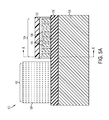
- FIGS. 1-14 are a series of views illustrating a method of forming a finFET device according to embodiments of the disclosure, in which:
- FIG. 1 is a cross-sectional view in a first orientation illustrating a semiconductor-on-insulator (SOI) starting substrate according to an exemplary embodiment
- FIG. 2 illustrates the substrate of FIG. 1 after patterning an active semiconductor layer to form a plurality of semiconductor fins on an insulator layer;
- FIG. 3A illustrates the substrate of FIG. 2 following formation of a dummy gate stack that wraps around an outer surface of the semiconductor fins to define a channel region;
- FIG. 3B is a cross-sectional view in a second orientation taken along the lines A-A′ of FIG. 3A ;
- FIG. 4A illustrates the substrate of FIGS. 3A-3B in the first orientation following formation spacers on sidewalls of the dummy gate stack;
- FIG. 4B is a cross-sectional view of the substrate illustrated in FIG. 4A according to the second orientation
- FIG. 5A illustrates the substrate of FIGS. 4A-4B in the first orientation after selectively growing a first epitaxial material on source/drain regions of the semiconductor fins formed in a pFET region of the substrate according to a first embodiment
- FIG. 5B is a cross-sectional view of the substrate illustrated in FIG. 5A according to the second orientation
- FIG. 6A illustrates the substrate of FIGS. 4A-4B in the first orientation after selectively growing a first epitaxial material on the semiconductor fins formed in a pFET region of the substrate and annealing the substrate to diffuse ions of the epitaxial material into the fin to form diffused extension regions according to a second embodiment
- FIG. 6B is a cross-sectional view of the substrate illustrated FIG. 6A according to the second orientation
- FIG. 7A illustrates the substrate of FIGS. 5A-5B in the first orientation after growing a second epitaxial material on the source/drain regions of the semiconductor fins formed in a nFET region of the substrate;
- FIG. 7B is a cross-sectional view taken along line B-B′ illustrating the substrate of FIG. 7A according to the second orientation;
- FIG. 8A illustrates the substrate of FIGS. 7A-7B following deposition of a dielectric layer that covers the semiconductor fins and the dummy gate stack in the nFET region and the pFET region;
- FIG. 8B illustrates the substrate of FIG. 8A according to the second orientation
- FIG. 9A illustrates the substrate of FIGS. 8A-8B following a replacement metal gate process that removes the dummy gate stack and exposes a portion of the semiconductor fins in the channel region of the pFET region;
- FIG. 9B illustrates the substrate of FIG. 9A according to the second orientation
- FIG. 9C is a third orientation of the substrate shown in FIGS. 9A-9B illustrating a cross-section of the semiconductor fins taken along line C-C′;
- FIG. 10A illustrates the substrate of FIGS. 9A-9C after partially etching the exposed portion of the semiconductor fins in the channel region;
- FIG. 10B illustrates the substrate of FIG. 10A according to the second orientation
- FIG. 10C illustrates the cross-section of the semiconductor fins shown in FIGS. 10A-10B according to the third orientation
- FIG. 11A illustrates the substrate of FIGS. 10A-10C in the first orientation after growing an epitaxial liner on the exposed portion of the semiconductor fins in the channel region to form an epi-lined channel region in the pFET region;
- FIG. 11B illustrates the substrate of FIG. 11A according to the second orientation
- FIG. 11C illustrates the cross-section of the semiconductor fins shown in FIGS. 11A-11B according to the third orientation
- FIG. 12 illustrates the substrate of FIGS. 11A-11C in the second orientation following formation of a metal gate stack that wraps around the epi-lined channel region
- FIG. 13 illustrates the substrate of FIG. 12 in the second orientation following formation of contact structures in the source/drain regions.
- FIG. 14 is a flow diagram illustrating a method of fabricating a semiconductor device according to an exemplary embodiment.
- a semiconductor-on-insulator (SOI) starting substrate 100 having one or more nFET regions 102 and one or more pFET regions 104 is generally shown.
- the SOI substrate 100 extends along a first axis (e.g., an X-axis) to define a width, a second axis (e.g., a Y-axis) to define a height and a third axis (e.g., Z-axis) to define a length.
- the nFET region 102 and the pFET region 104 form a CMOS device as understood by those ordinarily skilled in the art.
- the starting substrate is formed as a bulk semiconductor substrate.
- one or more doped wells are formed in regions of the substrate. The regions are doped with n-type atoms to form one or more pFET region, or p-type atoms to form one or more respective n regions as understood by those ordinarily skilled in the art.
- the SOI substrate 100 includes a bulk substrate layer 106 , an insulator layer 108 , and an active semiconductor layer 110 .
- the insulator layer 108 is formed as a buried oxide (BOX) layer 108 , for example, that is interposed between the bulk substrate layer 106 and the active semiconductor layer 110 to form the SOI substrate 100 as understood by those ordinarily skilled in the art.
- the BOX layer 108 is formed from various materials including, but not limited to, silicon dioxide (SiO 2 ).
- the bulk substrate layer 106 and the active semiconductor layer 110 is formed from various semiconductor materials including, but not limited to silicon (Si).
- the active semiconductor layer 110 is patterned according to a well-known sidewall image transfer (SIT) patterning process, for example. Accordingly, a plurality spaced regions 112 are formed in the active semiconductor layer 110 .
- the spaced regions 112 define a plurality of semiconductor fins 114 that are formed on the BOX layer 108 .
- the plurality of semiconductor fins 114 includes one or more n-type fins 114 formed in the nFET regions 102 and one or more pFET fins 114 formed in the pFET region 104 .
- Each of the fins 114 extends along the X-axis to define a respective first fin width (w FIN ), and extends from the BOX layer 108 along the Y-axis to define a fin height (h Fin ).
- a dummy gate stack 116 is formed atop the BOX layer 108 and extends along the X-axis using various gate stack formation processes understood by those ordinarily skilled in the art.
- the dummy gate stack 116 includes a hardmask layer 118 formed atop a dummy gate element 120 .
- the hardmask layer 118 is formed from, for example, silicon nitride (SN) and the dummy gate element 120 is formed from, for example, polysilicon (PC).
- the dummy gate element 120 wraps around a portion of each semiconductor fin 114 to define a gate channel region that extends along the Z-axis to define a channel length (l CHANNEL ).
- the length of gate channel region ultimately defines a respective channel region of the n-type fins 114 (i.e., an nFET channel region) and/or the p-type fins 114 (i.e., a PFET channel region).
- gate spacers 122 are formed on sidewalls of the dummy gate stack 116 .
- the gate spacers 122 may comprise nitride, and formed via a technique such as deposition of a conformal nitride layer. Sacrificial layers of the conformal nitride layer are removed such that the remaining nitride material forms the gate spacers 122 as understood by those ordinarily skilled in the art.
- the hardmask layer 118 protects the underlying dummy gate element 120 when etching the conformal spacer layer to form the gate spacers 122 .
- the gate spacers 122 are formed from various materials including, but not limited to, SiN.
- a first masking layer 124 is deposited on the BOX layer 108 such that the semiconductor fins 114 and the dummy gate stack 116 in the nFET region 102 and the pFET region 104 are covered.
- the first masking layer 124 is then selectively patterned to expose the pFET region 104 while covering the nFET region 102 . It is appreciated that the first masking layer 124 is instead patterned to expose the nFET region 102 while the pFET region 104 remains covered.
- a first epitaxial material 126 such as SiGe, for example, is grown on the exposed surfaces of the semiconductor fins 114 formed in the exposed pFET region 104 , for example.
- the first epitaxial material 126 is grown using various epitaxial growth processes understood by those ordinarily skilled in the art.
- the first epitaxial material 126 is also in-situ doped with p-type atoms such as boron, for example, as understood by those ordinarily skilled in the art.
- the first epitaxial material 126 covers opposing side portions of each semiconductor fin 114 located adjacent to opposing sides of the dummy gate stack 116 .
- the epitaxial material 126 and extends between a first end 128 of the fin 114 and a first spacer 122 of a first side of the fin 114 to define a first source/drain (S/D) region 130 , and between a second end 132 of the fin 114 and a second spacer 122 of the fin 114 to define a second S/D region 134 .
- a middle portion of the fins 114 located beneath the dummy gate element 120 and the gate spacers 122 exclude the epitaxial material 126 .
- nFET S/D region The S/D regions corresponding to the semiconductor fins 114 located in the nFET region 102 are referred to as nFET S/D region, and the S/D regions corresponding to the semiconductor fins 114 located in the pFET region 104 are referred to as the pFET S/D region.
- extension regions 133 are formed in portions of the fins 114 that are covered by the gate spacers 122 . More specifically, after selectively growing a first epitaxial material 126 on the semiconductor fins 114 formed in a pFET region 104 as described in detail above, the SOI substrate 100 undergoes a high-temperature annealing operation. The temperature ranges, for example, from approximately 900 degrees Celsius to approximately 1300 degrees Celsius. The annealing process diffuses the doped ions of the first epitaxial material 126 into the portions of the fin 114 located beneath the gate spacers 122 to form the extension regions 133 as illustrated in FIG. 6B . It is appreciated that the aforementioned annealing process is not limited to this stage of the process flow.
- a second masking layer 124 ′ is deposited on the BOX layer 108 , which covers the semiconductor fins 114 and the dummy gate stack 116 in the nFET region 102 and the pFET region 104 . It is appreciated that the first masking layer 124 is stripped before depositing the second masking layer 124 ′. The second masking layer 124 ′ is then selectively patterned to expose the nFET region 102 while covering the pFET region 104 .
- a second epitaxial material 135 is grown on the exposed surfaces of the semiconductor fins 114 formed in the exposed nFET region 102 , for example.
- the second epitaxial material 135 is grown using various epitaxial growth processes understood by those ordinarily skilled in the art.
- the second epitaxial material 135 such as silicon, for example, is also in-situ doped with n-type atoms such arsenic or phosphorus, for example, as understood by those ordinarily skilled in the art.
- the second epitaxial material 135 covers each semiconductor fin 114 and extends between a first end 128 of the fin 114 and a first spacer 122 to define a first S/D region 130 , and between a second end 132 of the fin 114 and a second spacer to define a second S/D region 134 .
- the portions of the fin 114 located beneath the dummy gate element 120 and the gate spacers 122 exclude the second epitaxial material 135 .
- An optional thermal annealing process is performed to diffuse the dopant atoms of the second epitaxial material 135 into the portions of the fins located beneath the gate spacers 122 to form extension regions as described in detail above with respect to FIGS. 5A-5B .
- the first and/or second masking layers 124 / 124 ′ are stripped away, and a dielectric layer 136 is deposited on the BOX layer 108 such that the S/D regions of the fins 114 and the gate stack 116 in both the nFET region 102 and the pFET region 104 are covered.
- the dielectric layer 136 is formed from various materials including, but not limited to, SiO 2 .
- the dielectric layer 136 is planarized according to a chemical-mechanical planarization (CMP) process as understood by those ordinarily skilled in the art. Accordingly, the upper surface of the hardmask layer 118 is formed flush with the upper surface of the dielectric layer 136 as further illustrated in FIG. 8B .
- CMP chemical-mechanical planarization
- a third masking layer 124 ′′′ is deposited on the dielectric layer 136 .
- the third masking layer 124 ′′′ is then selectively patterned to expose the pFET region 104 while covering the nFET region 102 . It is appreciated that the masking layer 124 ′′′ is instead patterned to expose the nFET region 102 while the pFET region 104 remains covered.
- each exposed fin portion 114 ′ has an initial fin width (w FIN1 ) and an initial fin height (h FIN1 ).
- the exposed fin portions 114 ′ are selectively etched with respect to the BOX layer 108 , the gate spacers 122 , and the dielectric layer 136 .
- a selective dry etching process is used, for example, to etch the exposed fin portions 114 ′.
- the BOX layer 108 , the gate spacers 122 and the dielectric layer 136 is formed from an oxide material, and a hydrochloric (HCl) gas, which is selective to oxide materials, is applied to the exposed fin portions 114 ′.
- HCl hydrochloric
- each side of the exposed fin portions 114 ′ is etched to reduce the width and/or height of the exposed fin portions 114 ′.
- a new fin width (w FIN2 ) and new fin height (h FIN2 ) is formed as illustrated in FIG. 10C .
- the surfaces of the exposed fin portions 114 ′ are reduced, for example, by approximately 2 nanometers (nm) to approximately 3 nm.
- an epitaxial liner 140 is grown on the etched surfaces of one or more of the exposed fin portions 114 ′.
- the combination of the epitaxial liner 140 and the underlying fins increases electron hole-mobility through the channel region of the fin portions 114 ′.
- the epitaxial liner 140 is formed, for example, by epitaxially growing silicon germanium (SiGe) on the etched surfaces of the exposed fin portions 114 ′.
- the germanium (Ge) concentration in the SiGe can range from approximately 10% to approximately 99%, for example. According to at least one embodiment, the germanium (Ge) concentration in the SiGe is range from 20% to 90%.
- the width of the epitaxial liner 140 equals or is approximately equal to the amount of material previously etched away from the surfaces of the exposed fin portions 114 ′.
- combination of the etched exposed fin portions 114 ′ and the epitaxial liner 140 defines a combined fin width (w FIN3 ) that is equal to or approximately equal to the initial fin width (w FIN1 ), and a combined fin height (h FIN3 ) that is equal to or approximately equal to the initial fin height (h FIN ) (see FIGS. 11B-11C ).
- the combination of the epitaxial liner 140 and a respective etched exposed fin portion 114 ′ forms an epitaxial-lined channel region 142 that modulates the threshold voltage (Vt) of the respective fin 114 .
- the epitaxial-lined channel region 142 is formed having a Vt of approximately ⁇ 0.3 V for approximately 25% SiGe, and approximately ⁇ 0.4 V for approximately 50% SiGe.
- the epitaxial-lined channel region 142 i.e., a SiGe liner formed on an etched portion of the semiconductor fin
- the channel regions of the nFET region consist only of Si.
- the nFET region excludes the SiGe liner from etched portions of the semiconductor fin (e.g., the middle portion of the fin).
- the pFET region 104 is formed having a first Vt and the nFET region 102 is formed having a different second Vt.
- the substrate may have multiple pFET regions. Each pFET region has a different concentration of SiGe with respect to one another.
- a first pFET may include a first epitaxial liner 140 having a 75% concentration of SiGe
- a second pFET may include a second epitaxial liner 140 having a 50% concentration of SiGe
- a third pFET region may include a third epitaxial liner 140 having a 25% concentration of SiGe
- a fourth pFET region may exclude a SiGe liner 140 (i.e., 0% concentration of SiGe). Accordingly, each pFET has a different Vt with respect to one another.
- the metal gate stack 144 that wraps around the epitaxial-lined channel region 142 is formed in the gate opening 138 .
- the metal gate stack 144 includes a gate dielectric layer 146 and a metal gate element 148 .
- the gate dielectric layer 146 is formed by depositing a conformal dielectric layer on the sidewalls of the gate spacers 122 and on the surfaces of the epitaxial-lined channel region 142 .
- the gate dielectric layer 146 is formed from various materials including, but not limited to, an oxide, nitride, and/or oxynitride material. In one example, the gate dielectric layer 146 is formed from a high k material having a dielectric constant greater than silicon dioxide.
- Exemplary high-k dielectrics include, but are not limited to, HfO 2 , ZrO 2 , La 2 O 3 , Al 2 O 3 TiO 2 , SrTiO 2 , LaAlO 3 , Y 2 O 3 , HfO x N y , ZrO x N y , La 2 O x N y , Al 2 O x N y , TiO z N y , SrTiO x N y , LaAlO x N y , Y 2 O x N y , SiON, SiN x , a silicate thereof, and an alloy thereof.
- the gate dielectric layer 146 is formed as a multilayered gate dielectric structure comprising different gate dielectric materials, including but not limited to, silicon dioxide, and a high-k gate dielectric material.
- the remaining gate opening 138 is filled with a metal material to form the metal gate element 148 .
- Any residual metal material and/or high-k material formed on an upper surface of the gate spacers 122 and/or dielectric layer 136 are planarized using a CMP process such that the metal gate stack 144 is formed and the high-k layer 146 interposed between the gate spacers 122 and the metal gate element 148 .
- the metal gate stack 144 also includes one or more work function metal (WFM) layers to further adjust the threshold voltage as understood by those ordinarily skilled in the art.
- WFM work function metal
- an electrically conductive contact structure 150 is formed at each S/D region 130 , 134 of the pFET region 104 .
- Each contact structure 150 includes a silicide portion 152 and an electrically conductive via 154 .
- the silicide portion 152 is embedded in the dielectric layer 136 and is formed on the first epitaxial material 126 .
- Various materials are used to form the silicide portion 152 including, but not limited to, CoSi 2 and NiSi.
- the via 154 is formed through the dielectric layer 136 such that a first end 156 contacts the silicide portion 152 and an opposite end 158 is exposed at an upper surface of the dielectric layer 136 .
- conductive contact structure 150 is formed in the pFET region in a similar manner as described above.
- a flow diagram illustrates a method of fabricating a semiconductor device including an epitaxial-lined channel region that adjusts a threshold voltage according to an exemplary embodiment.
- the method begins at operation 1400 , and at operation 1402 a semiconductor substrate including an nFET region and a pFET region is formed.
- a plurality of semiconductor fins is formed on an insulator layer of the semiconductor substrate.
- a dummy gate stack that wraps around a portion of the fins is formed on the insulator layer.
- spacers are formed on sidewalls of the dummy gate stack.
- a first epitaxial material is grown at S/D regions of the semiconductor fins formed in the pFET region.
- a second epitaxial material is grown at S/D regions of the semiconductor fins formed in the nFET region.
- a dielectric layer is formed on the insulator layer that covers the semiconductor fins and the dummy gate stack in the nFET and pFET regions at operation 1414 .
- a dummy gate element of the dummy gate stack is removed to form a gate opening that exposes a portion of the semiconductor fin. The exposed portion of the semiconductor fin is etched at operation 1418 .
- an epitaxial liner is grown on the etched portion of the semiconductor fin to form an epitaxial-lined channel region.
- a metal gate stack is formed that wraps around the epitaxial liner of the epitaxial-lined channel region, and the method ends at operation 1424 .
Abstract
Description
Claims (13)
Priority Applications (2)
| Application Number | Priority Date | Filing Date | Title |
|---|---|---|---|
| US14/729,105 US9275908B2 (en) | 2014-04-30 | 2015-06-03 | Semiconductor device including gate channel having adjusted threshold voltage |
| US14/984,231 US9530699B2 (en) | 2014-04-30 | 2015-12-30 | Semiconductor device including gate channel having adjusted threshold voltage |
Applications Claiming Priority (2)
| Application Number | Priority Date | Filing Date | Title |
|---|---|---|---|
| US14/265,735 US9230992B2 (en) | 2014-04-30 | 2014-04-30 | Semiconductor device including gate channel having adjusted threshold voltage |
| US14/729,105 US9275908B2 (en) | 2014-04-30 | 2015-06-03 | Semiconductor device including gate channel having adjusted threshold voltage |
Related Parent Applications (1)
| Application Number | Title | Priority Date | Filing Date |
|---|---|---|---|
| US14/265,735 Division US9230992B2 (en) | 2014-04-30 | 2014-04-30 | Semiconductor device including gate channel having adjusted threshold voltage |
Related Child Applications (1)
| Application Number | Title | Priority Date | Filing Date |
|---|---|---|---|
| US14/984,231 Continuation US9530699B2 (en) | 2014-04-30 | 2015-12-30 | Semiconductor device including gate channel having adjusted threshold voltage |
Publications (2)
| Publication Number | Publication Date |
|---|---|
| US20150318218A1 US20150318218A1 (en) | 2015-11-05 |
| US9275908B2 true US9275908B2 (en) | 2016-03-01 |
Family
ID=54355762
Family Applications (3)
| Application Number | Title | Priority Date | Filing Date |
|---|---|---|---|
| US14/265,735 Expired - Fee Related US9230992B2 (en) | 2014-04-30 | 2014-04-30 | Semiconductor device including gate channel having adjusted threshold voltage |
| US14/729,105 Expired - Fee Related US9275908B2 (en) | 2014-04-30 | 2015-06-03 | Semiconductor device including gate channel having adjusted threshold voltage |
| US14/984,231 Expired - Fee Related US9530699B2 (en) | 2014-04-30 | 2015-12-30 | Semiconductor device including gate channel having adjusted threshold voltage |
Family Applications Before (1)
| Application Number | Title | Priority Date | Filing Date |
|---|---|---|---|
| US14/265,735 Expired - Fee Related US9230992B2 (en) | 2014-04-30 | 2014-04-30 | Semiconductor device including gate channel having adjusted threshold voltage |
Family Applications After (1)
| Application Number | Title | Priority Date | Filing Date |
|---|---|---|---|
| US14/984,231 Expired - Fee Related US9530699B2 (en) | 2014-04-30 | 2015-12-30 | Semiconductor device including gate channel having adjusted threshold voltage |
Country Status (1)
| Country | Link |
|---|---|
| US (3) | US9230992B2 (en) |
Cited By (1)
| Publication number | Priority date | Publication date | Assignee | Title |
|---|---|---|---|---|
| US9418900B1 (en) * | 2015-07-15 | 2016-08-16 | International Business Machines Corporation | Silicon germanium and silicon fins on oxide from bulk wafer |
Families Citing this family (5)
| Publication number | Priority date | Publication date | Assignee | Title |
|---|---|---|---|---|
| US9230992B2 (en) | 2014-04-30 | 2016-01-05 | International Business Machines Corporation | Semiconductor device including gate channel having adjusted threshold voltage |
| KR20160034492A (en) * | 2014-09-19 | 2016-03-30 | 삼성전자주식회사 | Method for forming patterns of semiconductor devices and semiconductor devices using the same |
| JP6036860B2 (en) * | 2015-01-19 | 2016-11-30 | マツダ株式会社 | Flex fuel engine |
| US10707331B2 (en) * | 2017-04-28 | 2020-07-07 | Taiwan Semiconductor Manufacturing Company, Ltd. | FinFET device with a reduced width |
| US10679901B2 (en) | 2018-08-14 | 2020-06-09 | International Business Machines Corporation | Differing device characteristics on a single wafer by selective etch |
Citations (10)
| Publication number | Priority date | Publication date | Assignee | Title |
|---|---|---|---|---|
| US20070032020A1 (en) * | 2005-06-29 | 2007-02-08 | Grebs Thomas E | Structures and methods for forming shielded gate field effect transistors |
| US20070090416A1 (en) | 2005-09-28 | 2007-04-26 | Doyle Brian S | CMOS devices with a single work function gate electrode and method of fabrication |
| US7238989B2 (en) | 2003-03-07 | 2007-07-03 | Taiwan Semiconductor Manufacturing Company, Ltd. | Strain balanced structure with a tensile strained silicon channel and a compressive strained silicon-germanium channel for CMOS performance enhancement |
| US20110024804A1 (en) | 2009-07-28 | 2011-02-03 | Taiwan Semiconductor Manufacturing Company, Ltd. | Method for forming high germanium concentration sige stressor |
| WO2012074872A2 (en) | 2010-12-01 | 2012-06-07 | Intel Corporation | Silicon and silicon germanium nanowire structures |
| US20120319211A1 (en) * | 2011-06-16 | 2012-12-20 | Taiwan Semiconductor Manufacturing Company, Ltd. | Strained channel field effect transistor |
| US8450165B2 (en) | 2007-05-14 | 2013-05-28 | Intel Corporation | Semiconductor device having tipless epitaxial source/drain regions |
| WO2013095651A1 (en) | 2011-12-23 | 2013-06-27 | Intel Corporation | Non-planar gate all-around device and method of fabrication thereof |
| US20140145242A1 (en) * | 2012-11-29 | 2014-05-29 | Taiwan Semiconductor Manufacturing Company, Ltd. | Fin-Last FinFET and Methods of Forming Same |
| US20150008490A1 (en) * | 2013-07-06 | 2015-01-08 | Semi Solutions Llc | Fluctuation Resistant FinFET |
Family Cites Families (1)
| Publication number | Priority date | Publication date | Assignee | Title |
|---|---|---|---|---|
| US9230992B2 (en) | 2014-04-30 | 2016-01-05 | International Business Machines Corporation | Semiconductor device including gate channel having adjusted threshold voltage |
-
2014
- 2014-04-30 US US14/265,735 patent/US9230992B2/en not_active Expired - Fee Related
-
2015
- 2015-06-03 US US14/729,105 patent/US9275908B2/en not_active Expired - Fee Related
- 2015-12-30 US US14/984,231 patent/US9530699B2/en not_active Expired - Fee Related
Patent Citations (10)
| Publication number | Priority date | Publication date | Assignee | Title |
|---|---|---|---|---|
| US7238989B2 (en) | 2003-03-07 | 2007-07-03 | Taiwan Semiconductor Manufacturing Company, Ltd. | Strain balanced structure with a tensile strained silicon channel and a compressive strained silicon-germanium channel for CMOS performance enhancement |
| US20070032020A1 (en) * | 2005-06-29 | 2007-02-08 | Grebs Thomas E | Structures and methods for forming shielded gate field effect transistors |
| US20070090416A1 (en) | 2005-09-28 | 2007-04-26 | Doyle Brian S | CMOS devices with a single work function gate electrode and method of fabrication |
| US8450165B2 (en) | 2007-05-14 | 2013-05-28 | Intel Corporation | Semiconductor device having tipless epitaxial source/drain regions |
| US20110024804A1 (en) | 2009-07-28 | 2011-02-03 | Taiwan Semiconductor Manufacturing Company, Ltd. | Method for forming high germanium concentration sige stressor |
| WO2012074872A2 (en) | 2010-12-01 | 2012-06-07 | Intel Corporation | Silicon and silicon germanium nanowire structures |
| US20120319211A1 (en) * | 2011-06-16 | 2012-12-20 | Taiwan Semiconductor Manufacturing Company, Ltd. | Strained channel field effect transistor |
| WO2013095651A1 (en) | 2011-12-23 | 2013-06-27 | Intel Corporation | Non-planar gate all-around device and method of fabrication thereof |
| US20140145242A1 (en) * | 2012-11-29 | 2014-05-29 | Taiwan Semiconductor Manufacturing Company, Ltd. | Fin-Last FinFET and Methods of Forming Same |
| US20150008490A1 (en) * | 2013-07-06 | 2015-01-08 | Semi Solutions Llc | Fluctuation Resistant FinFET |
Non-Patent Citations (5)
| Title |
|---|
| Choi et al., "Sub-20 nm CMOS FinFET technologies," Electron Devices Meeting, 2001. IEDM '01. Technical Digest. International. |
| Monfray et al., "Applications of SiGe Material for CMOS and Related Processing." Bipolar/BiCMOS Circuits and Technology Meeting, IEEE, 2006. |
| Seger, "Interaction of Ni with SiGe for electrical contacts in CMOS technology", A dissertation submitted to the Royal Institute of Technology, Stockholm, Sweden in partial fulfillment of the requirements for the degree of Doctor of Philosophy (Ph. D.), 2005. |
| Togo et al., "Phosphorus doped SiC Source Drain and SiGe channel for scaled bulk FinFETs," Electron Devices Meeting (IEDM), 2012 IEEE International. |
| Toh et al., "Impact Ionization Nanowire Transistor with Multiple-Gates, Silicon-Germanium Impact Ionization Region, and Sub-5 mV/decade Subtheshold Swing," Electron Devices Meeting, 2007. IEDM 2007. IEEE International. |
Cited By (1)
| Publication number | Priority date | Publication date | Assignee | Title |
|---|---|---|---|---|
| US9418900B1 (en) * | 2015-07-15 | 2016-08-16 | International Business Machines Corporation | Silicon germanium and silicon fins on oxide from bulk wafer |
Also Published As
| Publication number | Publication date |
|---|---|
| US20150318307A1 (en) | 2015-11-05 |
| US9230992B2 (en) | 2016-01-05 |
| US9530699B2 (en) | 2016-12-27 |
| US20160111340A1 (en) | 2016-04-21 |
| US20150318218A1 (en) | 2015-11-05 |
Similar Documents
| Publication | Publication Date | Title |
|---|---|---|
| US20210272952A1 (en) | A method of manufacturing a semiconductor device and a semiconductor device | |
| US9530699B2 (en) | Semiconductor device including gate channel having adjusted threshold voltage | |
| US10770591B2 (en) | Source/drain contacts for non-planar transistors | |
| US10325820B1 (en) | Source and drain isolation for CMOS nanosheet with one block mask | |
| TWI559544B (en) | Finfet device and method for manufacturing the same | |
| US7902541B2 (en) | Semiconductor nanowire with built-in stress | |
| TWI396283B (en) | Semiconductor device | |
| US8871584B2 (en) | Replacement source/drain finFET fabrication | |
| US9711417B2 (en) | Fin field effect transistor including a strained epitaxial semiconductor shell | |
| TW201735268A (en) | Method for fabricating multi-gate device | |
| US20130026539A1 (en) | Replacement source/drain finfet fabrication | |
| US9660035B2 (en) | Semiconductor device including superlattice SiGe/Si fin structure | |
| US9893181B1 (en) | Uniform gate length in vertical field effect transistors | |
| US20140001561A1 (en) | Cmos devices having strain source/drain regions and low contact resistance | |
| US20170330878A1 (en) | NOVEL METHOD TO FABRICATE VERTICAL NWs | |
| US20170062614A1 (en) | Semiconductor device including dual spacer and uniform epitaxial buffer interface of embedded sige source/drain | |
| US9922886B2 (en) | Silicon-germanium FinFET device with controlled junction | |
| US9450094B1 (en) | Semiconductor process and fin-shaped field effect transistor | |
| CN105633152B (en) | Semiconductor structure and manufacturing method thereof |
Legal Events
| Date | Code | Title | Description |
|---|---|---|---|
| AS | Assignment |
Owner name: INTERNATIONAL BUSINESS MACHINES CORPORATION, NEW Y Free format text: ASSIGNMENT OF ASSIGNORS INTEREST;ASSIGNORS:KERBER, PRANITA;OUYANG, QIQING C.;REZNICEK, ALEXANDER;SIGNING DATES FROM 20140428 TO 20140429;REEL/FRAME:035772/0397 |
|
| STCF | Information on status: patent grant |
Free format text: PATENTED CASE |
|
| FEPP | Fee payment procedure |
Free format text: MAINTENANCE FEE REMINDER MAILED (ORIGINAL EVENT CODE: REM.); ENTITY STATUS OF PATENT OWNER: LARGE ENTITY |
|
| LAPS | Lapse for failure to pay maintenance fees |
Free format text: PATENT EXPIRED FOR FAILURE TO PAY MAINTENANCE FEES (ORIGINAL EVENT CODE: EXP.); ENTITY STATUS OF PATENT OWNER: LARGE ENTITY |
|
| STCH | Information on status: patent discontinuation |
Free format text: PATENT EXPIRED DUE TO NONPAYMENT OF MAINTENANCE FEES UNDER 37 CFR 1.362 |
|
| FP | Expired due to failure to pay maintenance fee |
Effective date: 20200301 |
|
| AS | Assignment |
Owner name: ELPIS TECHNOLOGIES INC., CANADA Free format text: ASSIGNMENT OF ASSIGNORS INTEREST;ASSIGNOR:INTERNATIONAL BUSINESS MACHINES CORPORATION;REEL/FRAME:052620/0961 Effective date: 20200306 |