US9252229B2 - Inversion thickness reduction in high-k gate stacks formed by replacement gate processes - Google Patents
Inversion thickness reduction in high-k gate stacks formed by replacement gate processes Download PDFInfo
- Publication number
- US9252229B2 US9252229B2 US13/605,267 US201213605267A US9252229B2 US 9252229 B2 US9252229 B2 US 9252229B2 US 201213605267 A US201213605267 A US 201213605267A US 9252229 B2 US9252229 B2 US 9252229B2
- Authority
- US
- United States
- Prior art keywords
- layer
- gate
- metal
- doped
- dielectric
- Prior art date
- Legal status (The legal status is an assumption and is not a legal conclusion. Google has not performed a legal analysis and makes no representation as to the accuracy of the status listed.)
- Expired - Fee Related, expires
Links
- 238000000034 method Methods 0.000 title abstract description 38
- 230000008569 process Effects 0.000 title abstract description 21
- 230000009467 reduction Effects 0.000 title description 3
- 229910052751 metal Inorganic materials 0.000 claims abstract description 93
- 239000002184 metal Substances 0.000 claims abstract description 93
- 239000000463 material Substances 0.000 claims abstract description 42
- 239000004065 semiconductor Substances 0.000 claims abstract description 36
- 239000000758 substrate Substances 0.000 claims abstract description 29
- 230000002000 scavenging effect Effects 0.000 claims description 33
- 125000006850 spacer group Chemical group 0.000 claims description 11
- 229910000765 intermetallic Inorganic materials 0.000 claims description 9
- 229910052782 aluminium Inorganic materials 0.000 claims description 8
- QVGXLLKOCUKJST-UHFFFAOYSA-N atomic oxygen Chemical compound [O] QVGXLLKOCUKJST-UHFFFAOYSA-N 0.000 claims description 8
- 239000001301 oxygen Substances 0.000 claims description 8
- 229910052760 oxygen Inorganic materials 0.000 claims description 8
- 229910052723 transition metal Inorganic materials 0.000 claims description 7
- ATJFFYVFTNAWJD-UHFFFAOYSA-N Tin Chemical compound [Sn] ATJFFYVFTNAWJD-UHFFFAOYSA-N 0.000 claims description 6
- -1 transition metal nitride Chemical class 0.000 claims description 5
- 150000003624 transition metals Chemical class 0.000 claims description 5
- 229910052735 hafnium Inorganic materials 0.000 claims description 4
- 229910044991 metal oxide Inorganic materials 0.000 claims description 4
- 150000004706 metal oxides Chemical class 0.000 claims description 4
- 229910052715 tantalum Inorganic materials 0.000 claims description 3
- 229910052719 titanium Inorganic materials 0.000 claims description 3
- 229910052684 Cerium Inorganic materials 0.000 claims description 2
- 229910052790 beryllium Inorganic materials 0.000 claims description 2
- 229910052791 calcium Inorganic materials 0.000 claims description 2
- 230000008859 change Effects 0.000 claims description 2
- 238000006243 chemical reaction Methods 0.000 claims description 2
- 229910052746 lanthanum Inorganic materials 0.000 claims description 2
- 229910052749 magnesium Inorganic materials 0.000 claims description 2
- 229910052712 strontium Inorganic materials 0.000 claims description 2
- 229910052727 yttrium Inorganic materials 0.000 claims description 2
- 229910052726 zirconium Inorganic materials 0.000 claims description 2
- 125000004430 oxygen atom Chemical group O* 0.000 abstract description 9
- 239000010410 layer Substances 0.000 description 150
- VYPSYNLAJGMNEJ-UHFFFAOYSA-N Silicium dioxide Chemical compound O=[Si]=O VYPSYNLAJGMNEJ-UHFFFAOYSA-N 0.000 description 27
- 239000003989 dielectric material Substances 0.000 description 13
- 239000000126 substance Substances 0.000 description 13
- 230000015572 biosynthetic process Effects 0.000 description 12
- 239000000377 silicon dioxide Substances 0.000 description 11
- 125000004429 atom Chemical group 0.000 description 8
- 229910021420 polycrystalline silicon Inorganic materials 0.000 description 8
- XUIMIQQOPSSXEZ-UHFFFAOYSA-N Silicon Chemical compound [Si] XUIMIQQOPSSXEZ-UHFFFAOYSA-N 0.000 description 7
- 238000000151 deposition Methods 0.000 description 7
- 229920005591 polysilicon Polymers 0.000 description 7
- 229910052710 silicon Inorganic materials 0.000 description 7
- 239000010703 silicon Substances 0.000 description 7
- UQZIWOQVLUASCR-UHFFFAOYSA-N alumane;titanium Chemical compound [AlH3].[Ti] UQZIWOQVLUASCR-UHFFFAOYSA-N 0.000 description 6
- 229910021419 crystalline silicon Inorganic materials 0.000 description 6
- 230000008021 deposition Effects 0.000 description 5
- 239000002019 doping agent Substances 0.000 description 5
- 230000005669 field effect Effects 0.000 description 5
- 229910052814 silicon oxide Inorganic materials 0.000 description 5
- 239000010936 titanium Substances 0.000 description 5
- 229910052581 Si3N4 Inorganic materials 0.000 description 4
- NRTOMJZYCJJWKI-UHFFFAOYSA-N Titanium nitride Chemical compound [Ti]#N NRTOMJZYCJJWKI-UHFFFAOYSA-N 0.000 description 4
- RVSGESPTHDDNTH-UHFFFAOYSA-N alumane;tantalum Chemical compound [AlH3].[Ta] RVSGESPTHDDNTH-UHFFFAOYSA-N 0.000 description 4
- XAGFODPZIPBFFR-UHFFFAOYSA-N aluminium Chemical compound [Al] XAGFODPZIPBFFR-UHFFFAOYSA-N 0.000 description 4
- 239000004020 conductor Substances 0.000 description 4
- 230000000694 effects Effects 0.000 description 4
- HQVNEWCFYHHQES-UHFFFAOYSA-N silicon nitride Chemical compound N12[Si]34N5[Si]62N3[Si]51N64 HQVNEWCFYHHQES-UHFFFAOYSA-N 0.000 description 4
- 229910001339 C alloy Inorganic materials 0.000 description 3
- 238000000231 atomic layer deposition Methods 0.000 description 3
- 238000005229 chemical vapour deposition Methods 0.000 description 3
- 150000001875 compounds Chemical class 0.000 description 3
- 239000007772 electrode material Substances 0.000 description 3
- 239000012212 insulator Substances 0.000 description 3
- 229910003468 tantalcarbide Inorganic materials 0.000 description 3
- MZLGASXMSKOWSE-UHFFFAOYSA-N tantalum nitride Chemical compound [Ta]#N MZLGASXMSKOWSE-UHFFFAOYSA-N 0.000 description 3
- 230000005641 tunneling Effects 0.000 description 3
- IJGRMHOSHXDMSA-UHFFFAOYSA-N Atomic nitrogen Chemical compound N#N IJGRMHOSHXDMSA-UHFFFAOYSA-N 0.000 description 2
- KRHYYFGTRYWZRS-UHFFFAOYSA-N Fluorane Chemical compound F KRHYYFGTRYWZRS-UHFFFAOYSA-N 0.000 description 2
- MHAJPDPJQMAIIY-UHFFFAOYSA-N Hydrogen peroxide Chemical compound OO MHAJPDPJQMAIIY-UHFFFAOYSA-N 0.000 description 2
- KDLHZDBZIXYQEI-UHFFFAOYSA-N Palladium Chemical compound [Pd] KDLHZDBZIXYQEI-UHFFFAOYSA-N 0.000 description 2
- 229910000676 Si alloy Inorganic materials 0.000 description 2
- GWEVSGVZZGPLCZ-UHFFFAOYSA-N Titan oxide Chemical compound O=[Ti]=O GWEVSGVZZGPLCZ-UHFFFAOYSA-N 0.000 description 2
- MCMNRKCIXSYSNV-UHFFFAOYSA-N Zirconium dioxide Chemical compound O=[Zr]=O MCMNRKCIXSYSNV-UHFFFAOYSA-N 0.000 description 2
- AXQKVSDUCKWEKE-UHFFFAOYSA-N [C].[Ge].[Si] Chemical compound [C].[Ge].[Si] AXQKVSDUCKWEKE-UHFFFAOYSA-N 0.000 description 2
- LEVVHYCKPQWKOP-UHFFFAOYSA-N [Si].[Ge] Chemical compound [Si].[Ge] LEVVHYCKPQWKOP-UHFFFAOYSA-N 0.000 description 2
- CEPICIBPGDWCRU-UHFFFAOYSA-N [Si].[Hf] Chemical compound [Si].[Hf] CEPICIBPGDWCRU-UHFFFAOYSA-N 0.000 description 2
- 230000002411 adverse Effects 0.000 description 2
- 229910052784 alkaline earth metal Inorganic materials 0.000 description 2
- 150000001342 alkaline earth metals Chemical class 0.000 description 2
- 229910045601 alloy Inorganic materials 0.000 description 2
- 239000000956 alloy Substances 0.000 description 2
- 230000008901 benefit Effects 0.000 description 2
- 230000005684 electric field Effects 0.000 description 2
- 238000005516 engineering process Methods 0.000 description 2
- 238000005468 ion implantation Methods 0.000 description 2
- 238000002955 isolation Methods 0.000 description 2
- 238000004519 manufacturing process Methods 0.000 description 2
- 150000002736 metal compounds Chemical class 0.000 description 2
- 150000002739 metals Chemical class 0.000 description 2
- NFFIWVVINABMKP-UHFFFAOYSA-N methylidynetantalum Chemical compound [Ta]#C NFFIWVVINABMKP-UHFFFAOYSA-N 0.000 description 2
- 239000000203 mixture Substances 0.000 description 2
- 238000002161 passivation Methods 0.000 description 2
- BASFCYQUMIYNBI-UHFFFAOYSA-N platinum Chemical compound [Pt] BASFCYQUMIYNBI-UHFFFAOYSA-N 0.000 description 2
- 238000004549 pulsed laser deposition Methods 0.000 description 2
- 235000012239 silicon dioxide Nutrition 0.000 description 2
- WFKWXMTUELFFGS-UHFFFAOYSA-N tungsten Chemical compound [W] WFKWXMTUELFFGS-UHFFFAOYSA-N 0.000 description 2
- 229910052721 tungsten Inorganic materials 0.000 description 2
- 239000010937 tungsten Substances 0.000 description 2
- VHUUQVKOLVNVRT-UHFFFAOYSA-N Ammonium hydroxide Chemical compound [NH4+].[OH-] VHUUQVKOLVNVRT-UHFFFAOYSA-N 0.000 description 1
- JBRZTFJDHDCESZ-UHFFFAOYSA-N AsGa Chemical compound [As]#[Ga] JBRZTFJDHDCESZ-UHFFFAOYSA-N 0.000 description 1
- RYGMFSIKBFXOCR-UHFFFAOYSA-N Copper Chemical compound [Cu] RYGMFSIKBFXOCR-UHFFFAOYSA-N 0.000 description 1
- 229910001218 Gallium arsenide Inorganic materials 0.000 description 1
- 229910000927 Ge alloy Inorganic materials 0.000 description 1
- 229910000673 Indium arsenide Inorganic materials 0.000 description 1
- GPXJNWSHGFTCBW-UHFFFAOYSA-N Indium phosphide Chemical compound [In]#P GPXJNWSHGFTCBW-UHFFFAOYSA-N 0.000 description 1
- 229910002244 LaAlO3 Inorganic materials 0.000 description 1
- BPQQTUXANYXVAA-UHFFFAOYSA-N Orthosilicate Chemical compound [O-][Si]([O-])([O-])[O-] BPQQTUXANYXVAA-UHFFFAOYSA-N 0.000 description 1
- CBENFWSGALASAD-UHFFFAOYSA-N Ozone Chemical compound [O-][O+]=O CBENFWSGALASAD-UHFFFAOYSA-N 0.000 description 1
- KJTLSVCANCCWHF-UHFFFAOYSA-N Ruthenium Chemical compound [Ru] KJTLSVCANCCWHF-UHFFFAOYSA-N 0.000 description 1
- 229910000577 Silicon-germanium Inorganic materials 0.000 description 1
- 229910002370 SrTiO3 Inorganic materials 0.000 description 1
- 229910004166 TaN Inorganic materials 0.000 description 1
- 229910010303 TiOxNy Inorganic materials 0.000 description 1
- RTAQQCXQSZGOHL-UHFFFAOYSA-N Titanium Chemical compound [Ti] RTAQQCXQSZGOHL-UHFFFAOYSA-N 0.000 description 1
- 229910003134 ZrOx Inorganic materials 0.000 description 1
- HMDDXIMCDZRSNE-UHFFFAOYSA-N [C].[Si] Chemical compound [C].[Si] HMDDXIMCDZRSNE-UHFFFAOYSA-N 0.000 description 1
- 229910052768 actinide Inorganic materials 0.000 description 1
- 150000001255 actinides Chemical class 0.000 description 1
- PNEYBMLMFCGWSK-UHFFFAOYSA-N aluminium oxide Inorganic materials [O-2].[O-2].[O-2].[Al+3].[Al+3] PNEYBMLMFCGWSK-UHFFFAOYSA-N 0.000 description 1
- 239000000908 ammonium hydroxide Substances 0.000 description 1
- 229910021417 amorphous silicon Inorganic materials 0.000 description 1
- 230000003321 amplification Effects 0.000 description 1
- 238000000137 annealing Methods 0.000 description 1
- 239000007864 aqueous solution Substances 0.000 description 1
- 238000005234 chemical deposition Methods 0.000 description 1
- 230000000295 complement effect Effects 0.000 description 1
- 239000002131 composite material Substances 0.000 description 1
- 229910052802 copper Inorganic materials 0.000 description 1
- 239000010949 copper Substances 0.000 description 1
- 229910052593 corundum Inorganic materials 0.000 description 1
- 238000001914 filtration Methods 0.000 description 1
- 229910052732 germanium Inorganic materials 0.000 description 1
- GNPVGFCGXDBREM-UHFFFAOYSA-N germanium atom Chemical compound [Ge] GNPVGFCGXDBREM-UHFFFAOYSA-N 0.000 description 1
- 239000011521 glass Substances 0.000 description 1
- CJNBYAVZURUTKZ-UHFFFAOYSA-N hafnium(IV) oxide Inorganic materials O=[Hf]=O CJNBYAVZURUTKZ-UHFFFAOYSA-N 0.000 description 1
- 239000007943 implant Substances 0.000 description 1
- 239000012535 impurity Substances 0.000 description 1
- RPQDHPTXJYYUPQ-UHFFFAOYSA-N indium arsenide Chemical compound [In]#[As] RPQDHPTXJYYUPQ-UHFFFAOYSA-N 0.000 description 1
- 230000001939 inductive effect Effects 0.000 description 1
- 229910052741 iridium Inorganic materials 0.000 description 1
- GKOZUEZYRPOHIO-UHFFFAOYSA-N iridium atom Chemical compound [Ir] GKOZUEZYRPOHIO-UHFFFAOYSA-N 0.000 description 1
- 229910052747 lanthanoid Inorganic materials 0.000 description 1
- 150000002602 lanthanoids Chemical class 0.000 description 1
- MRELNEQAGSRDBK-UHFFFAOYSA-N lanthanum oxide Inorganic materials [O-2].[O-2].[O-2].[La+3].[La+3] MRELNEQAGSRDBK-UHFFFAOYSA-N 0.000 description 1
- 239000007788 liquid Substances 0.000 description 1
- 239000007769 metal material Substances 0.000 description 1
- 230000004048 modification Effects 0.000 description 1
- 238000012986 modification Methods 0.000 description 1
- 229910052757 nitrogen Inorganic materials 0.000 description 1
- 230000006911 nucleation Effects 0.000 description 1
- 238000010899 nucleation Methods 0.000 description 1
- 238000003199 nucleic acid amplification method Methods 0.000 description 1
- 238000005457 optimization Methods 0.000 description 1
- 230000003647 oxidation Effects 0.000 description 1
- 238000007254 oxidation reaction Methods 0.000 description 1
- KTUFCUMIWABKDW-UHFFFAOYSA-N oxo(oxolanthaniooxy)lanthanum Chemical compound O=[La]O[La]=O KTUFCUMIWABKDW-UHFFFAOYSA-N 0.000 description 1
- 229910052763 palladium Inorganic materials 0.000 description 1
- 230000000737 periodic effect Effects 0.000 description 1
- 229910052697 platinum Inorganic materials 0.000 description 1
- 238000005498 polishing Methods 0.000 description 1
- 238000002360 preparation method Methods 0.000 description 1
- 238000013139 quantization Methods 0.000 description 1
- 229910052702 rhenium Inorganic materials 0.000 description 1
- WUAPFZMCVAUBPE-UHFFFAOYSA-N rhenium atom Chemical compound [Re] WUAPFZMCVAUBPE-UHFFFAOYSA-N 0.000 description 1
- 229910052707 ruthenium Inorganic materials 0.000 description 1
- 229910021332 silicide Inorganic materials 0.000 description 1
- FVBUAEGBCNSCDD-UHFFFAOYSA-N silicide(4-) Chemical compound [Si-4] FVBUAEGBCNSCDD-UHFFFAOYSA-N 0.000 description 1
- 229910021483 silicon-carbon alloy Inorganic materials 0.000 description 1
- 239000002356 single layer Substances 0.000 description 1
- 238000000992 sputter etching Methods 0.000 description 1
- GUVRBAGPIYLISA-UHFFFAOYSA-N tantalum atom Chemical compound [Ta] GUVRBAGPIYLISA-UHFFFAOYSA-N 0.000 description 1
- XLYOFNOQVPJJNP-UHFFFAOYSA-N water Substances O XLYOFNOQVPJJNP-UHFFFAOYSA-N 0.000 description 1
- 229910001845 yogo sapphire Inorganic materials 0.000 description 1
- RUDFQVOCFDJEEF-UHFFFAOYSA-N yttrium(III) oxide Inorganic materials [O-2].[O-2].[O-2].[Y+3].[Y+3] RUDFQVOCFDJEEF-UHFFFAOYSA-N 0.000 description 1
Images


Classifications
-
- H—ELECTRICITY
- H01—ELECTRIC ELEMENTS
- H01L—SEMICONDUCTOR DEVICES NOT COVERED BY CLASS H10
- H01L29/00—Semiconductor devices adapted for rectifying, amplifying, oscillating or switching, or capacitors or resistors with at least one potential-jump barrier or surface barrier, e.g. PN junction depletion layer or carrier concentration layer; Details of semiconductor bodies or of electrodes thereof ; Multistep manufacturing processes therefor
- H01L29/40—Electrodes ; Multistep manufacturing processes therefor
- H01L29/43—Electrodes ; Multistep manufacturing processes therefor characterised by the materials of which they are formed
- H01L29/49—Metal-insulator-semiconductor electrodes, e.g. gates of MOSFET
- H01L29/4966—Metal-insulator-semiconductor electrodes, e.g. gates of MOSFET the conductor material next to the insulator being a composite material, e.g. organic material, TiN, MoSi2
-
- H—ELECTRICITY
- H01—ELECTRIC ELEMENTS
- H01L—SEMICONDUCTOR DEVICES NOT COVERED BY CLASS H10
- H01L21/00—Processes or apparatus adapted for the manufacture or treatment of semiconductor or solid state devices or of parts thereof
- H01L21/02—Manufacture or treatment of semiconductor devices or of parts thereof
- H01L21/04—Manufacture or treatment of semiconductor devices or of parts thereof the devices having at least one potential-jump barrier or surface barrier, e.g. PN junction, depletion layer or carrier concentration layer
- H01L21/18—Manufacture or treatment of semiconductor devices or of parts thereof the devices having at least one potential-jump barrier or surface barrier, e.g. PN junction, depletion layer or carrier concentration layer the devices having semiconductor bodies comprising elements of Group IV of the Periodic System or AIIIBV compounds with or without impurities, e.g. doping materials
- H01L21/28—Manufacture of electrodes on semiconductor bodies using processes or apparatus not provided for in groups H01L21/20 - H01L21/268
- H01L21/28008—Making conductor-insulator-semiconductor electrodes
- H01L21/28017—Making conductor-insulator-semiconductor electrodes the insulator being formed after the semiconductor body, the semiconductor being silicon
- H01L21/28158—Making the insulator
- H01L21/28167—Making the insulator on single crystalline silicon, e.g. using a liquid, i.e. chemical oxidation
- H01L21/28176—Making the insulator on single crystalline silicon, e.g. using a liquid, i.e. chemical oxidation with a treatment, e.g. annealing, after the formation of the definitive gate conductor
-
- H—ELECTRICITY
- H01—ELECTRIC ELEMENTS
- H01L—SEMICONDUCTOR DEVICES NOT COVERED BY CLASS H10
- H01L29/00—Semiconductor devices adapted for rectifying, amplifying, oscillating or switching, or capacitors or resistors with at least one potential-jump barrier or surface barrier, e.g. PN junction depletion layer or carrier concentration layer; Details of semiconductor bodies or of electrodes thereof ; Multistep manufacturing processes therefor
- H01L29/40—Electrodes ; Multistep manufacturing processes therefor
- H01L29/43—Electrodes ; Multistep manufacturing processes therefor characterised by the materials of which they are formed
- H01L29/49—Metal-insulator-semiconductor electrodes, e.g. gates of MOSFET
- H01L29/51—Insulating materials associated therewith
- H01L29/517—Insulating materials associated therewith the insulating material comprising a metallic compound, e.g. metal oxide, metal silicate
-
- H—ELECTRICITY
- H01—ELECTRIC ELEMENTS
- H01L—SEMICONDUCTOR DEVICES NOT COVERED BY CLASS H10
- H01L29/00—Semiconductor devices adapted for rectifying, amplifying, oscillating or switching, or capacitors or resistors with at least one potential-jump barrier or surface barrier, e.g. PN junction depletion layer or carrier concentration layer; Details of semiconductor bodies or of electrodes thereof ; Multistep manufacturing processes therefor
- H01L29/66—Types of semiconductor device ; Multistep manufacturing processes therefor
- H01L29/66007—Multistep manufacturing processes
- H01L29/66075—Multistep manufacturing processes of devices having semiconductor bodies comprising group 14 or group 13/15 materials
- H01L29/66227—Multistep manufacturing processes of devices having semiconductor bodies comprising group 14 or group 13/15 materials the devices being controllable only by the electric current supplied or the electric potential applied, to an electrode which does not carry the current to be rectified, amplified or switched, e.g. three-terminal devices
- H01L29/66409—Unipolar field-effect transistors
- H01L29/66477—Unipolar field-effect transistors with an insulated gate, i.e. MISFET
- H01L29/66568—Lateral single gate silicon transistors
- H01L29/66606—Lateral single gate silicon transistors with final source and drain contacts formation strictly before final or dummy gate formation, e.g. contact first technology
-
- H—ELECTRICITY
- H01—ELECTRIC ELEMENTS
- H01L—SEMICONDUCTOR DEVICES NOT COVERED BY CLASS H10
- H01L29/00—Semiconductor devices adapted for rectifying, amplifying, oscillating or switching, or capacitors or resistors with at least one potential-jump barrier or surface barrier, e.g. PN junction depletion layer or carrier concentration layer; Details of semiconductor bodies or of electrodes thereof ; Multistep manufacturing processes therefor
- H01L29/66—Types of semiconductor device ; Multistep manufacturing processes therefor
- H01L29/68—Types of semiconductor device ; Multistep manufacturing processes therefor controllable by only the electric current supplied, or only the electric potential applied, to an electrode which does not carry the current to be rectified, amplified or switched
- H01L29/76—Unipolar devices, e.g. field effect transistors
- H01L29/772—Field effect transistors
- H01L29/78—Field effect transistors with field effect produced by an insulated gate
- H01L29/7833—Field effect transistors with field effect produced by an insulated gate with lightly doped drain or source extension, e.g. LDD MOSFET's; DDD MOSFET's
Definitions
- the present invention relates generally to semiconductor device manufacturing and, more particularly, to methods and structures for achieving inversion thickness (T inv ) reduction in high-k gate stacks formed by replacement gate processes.
- FETs Field effect transistors
- MOSFET metal-oxide-semiconductor field-effect transistors
- CMOS Complementary MOS
- NMOS and PMOS n-type and p-type transistors are used to fabricate logic and other circuitry.
- the source and drain regions of an FET are typically formed by adding dopants to targeted regions of a semiconductor body on either side of the channel.
- a gate structure is formed above the channel, which includes a gate dielectric located over the channel and a gate conductor above the gate dielectric.
- the gate dielectric is an insulator material, which prevents large leakage currents from flowing into the channel when a voltage is applied to the gate conductor, while allowing the applied gate voltage to set up a transverse electric field in the channel region in a controllable manner.
- MOS transistors typically include a gate dielectric formed by depositing or by growing silicon dioxide (SiO 2 ) or silicon oxynitride (SiON) over a silicon wafer surface, with doped polysilicon formed over the SiO 2 to act as the gate conductor.
- SiO 2 silicon dioxide
- SiON silicon oxynitride
- MOS transistor performance may be improved by reducing the distance between the source and the drain regions under the gate conductor of the device, known as the gate or channel length, and by reducing the thickness of the layer of gate dielectric that is formed over the semiconductor surface.
- the thickness of SiO 2 gate dielectrics can be reduced. For example, thin SiO 2 gate dielectrics are prone to gate tunneling leakage currents resulting from direct tunneling of electrons through the thin gate dielectric.
- Scaling of the gate dielectric is a challenge in improving performance of advanced field effect transistors.
- the leakage current through the gate dielectric increases exponentially with the decrease in the thickness of the gate dielectric.
- Such devices typically become too leaky to provide high performance at or below a thickness of about 1.1 nm for the silicon oxide gate dielectric.
- High-k dielectric materials having dielectric constants greater than that of SiO 2 (e.g., greater than about 3.9).
- High-k dielectric materials can be formed in a thicker layer than scaled SiO 2 , and yet still produce equivalent field effect performance.
- the relative electrical performance of such high-k dielectric materials is often expressed in terms equivalent oxide thickness (EOT), since the high-k material layer may be thicker, while still providing the equivalent electrical effect of a much thinner layer of SiO 2 .
- EOT equivalent oxide thickness
- the dielectric constant “k” is higher than silicon dioxide, a thicker high-k dielectric layer can be employed to mitigate tunneling leakage currents, while still achieving the equivalent electrical performance of a thinner layer of thermally grown SiO 2 .
- a method of forming a transistor device includes forming an interfacial layer on a semiconductor substrate, corresponding to a region between formed doped source and drain regions in the substrate; forming a high dielectric constant (high-k) layer on the interfacial layer, the high-k layer having a dielectric constant greater than about 7.5; forming a doped metal layer on the high-k layer; performing a thermal process so as to cause the doped metal layer to scavenge oxygen atoms diffused from the interfacial layer such that a final thickness of the interfacial layer is less than about 5 angstroms ( ⁇ ); and forming a metal gate material over the high-k dielectric layer.
- high-k high dielectric constant
- ⁇ angstroms
- a method of forming a transistor device includes forming a chemical oxide interfacial layer on a semiconductor substrate, corresponding to a region between formed doped source and drain regions in the substrate, and between preformed gate sidewall spacers in accordance with a replacement gate scheme; forming a high dielectric constant (high-k) layer over an interlevel dielectric layer, on sidewalls of the sidewall spacers, and on the chemical oxide interfacial layer, the high-k layer having a dielectric constant greater than about 7.5; forming a doped metal layer on the high-k layer; performing an anneal in an H 2 ambient environment, at a temperature range of about 400° C.
- high-k high dielectric constant
- a method of forming a transistor device includes forming a chemical oxide interfacial layer on a semiconductor substrate, corresponding to a region between formed doped source and drain regions in the substrate, and between preformed gate sidewall spacers in accordance with a replacement gate scheme; forming a high dielectric constant (high-k) layer over an interlevel dielectric layer, on sidewalls of the sidewall spacers, and on the chemical oxide interfacial layer, the high-k layer having a dielectric constant greater than about 7.5; forming a doped metal layer on the high-k layer; forming a sacrificial layer over the doped metal layer, at a deposition temperature range of about 500° C.
- high-k high dielectric constant
- the doped metal layer to scavenge oxygen atoms diffused from the chemical oxide interfacial layer interfacial layer such that a final thickness of the chemical oxide interfacial layer interfacial layer is less than about 5 angstroms ( ⁇ ); removing the sacrificial layer; and forming a metal gate material over the high-k dielectric layer, within a recess defined by removal of a dummy gate structure initially used to form the source and drain regions in the substrate.
- a transistor device in still another aspect, includes an interfacial layer formed on a semiconductor substrate, corresponding to a region between doped source and drain regions in the substrate, the interfacial layer having a thickness less than about 5 angstroms ( ⁇ ); a high dielectric constant (high-k) layer formed on the interfacial layer, the high-k layer having a dielectric constant greater than about 7.5, the high-k layer having vertical sidewalls abutting vertical sidewalls of gate sidewall spacers; and a metal gate material formed over the high-k dielectric layer.
- ⁇ angstroms
- FIGS. 1 through 8 are cross sectional views of an exemplary embodiment of a method of forming high-k gate stacks for an FET device by replacement gate processing, in which:
- FIG. 1 illustrates the removal of a sacrificial dummy gate structure formed on a semiconductor substrate
- FIG. 2 illustrates the formation of an interfacial layer (IL) and high-k dielectric layer over the structure of FIG. 1 ;
- IL interfacial layer
- FIG. 3 illustrates the formation of a doped metal layer and a sacrificial polysilicon layer over the structure of FIG. 2 , resulting in scavenging of oxygen atoms from the IL;
- FIG. 4 illustrates an optional rapid thermal anneal of the structure of FIG. 3 for IL passivation
- FIG. 5 illustrates the removal of the sacrificial polysilicon layer and the doped metal layer of the structure of FIG. 4 ;
- FIG. 6 illustrates an optional anneal of the structure of FIG. 5 in an oxygen ambient so as to reduce gate leakage current
- FIG. 7 illustrates the formation of a metal gate electrode material over the structure of 5 ;
- FIG. 8 illustrates planarization of the structure of FIG. 7 so as to define a high-k, metal gate transistor structure
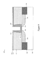
- FIGS. 9 through 11 are cross sectional views of another exemplary embodiment of a method of forming high-k gate stacks for an FET device by replacement gate processing, in which:
- FIG. 9 illustrates the removal of only the sacrificial polysilicon layer of the structure of FIG. 4 , leaving the doped metal layer;
- FIG. 10 illustrates the formation of a metal gate electrode material over the structure of 9 ;
- FIG. 11 illustrates planarization of the structure of FIG. 10 so as to define a high-k, metal gate transistor structure
- FIGS. 12 and 13 are cross sectional views of another exemplary embodiment of a method of forming high-k gate stacks for an FET device by replacement gate processing, in which:
- FIG. 12 illustrates the formation of an interfacial layer (IL), a high-k dielectric layer, and a doped metal layer over the structure of FIG. 1 ;
- FIG. 13 illustrates an anneal of the structure of FIG. 11 , resulting in scavenging of oxygen atoms from the IL.
- inversion thickness also referred to simply as “inversion thickness” (T inv )
- inversion thickness measures the incremental inversion charge density per gate voltage swing. Due to inversion layer quantization and polysilicon gate depletion effects, T inv is thicker than EOT. As such, scaling of EOT also results in scaling of T inv .
- interfacial layer (IL) scavenging In which a metal scavenging layer present in the gate stack captures oxygen atoms that diffuse, during high temperature annealing, from a bottom interface layer formed between the semiconductor substrate and the high-k dielectric layer. While such a technique is promising with respect to “gate first” high-k gate processes, T inv scaling has not heretofore been reported for high-k gate stacks fabricated by replacement gate processes.
- IL interfacial layer
- a replacement gate process architecture avoids the problems of work function material stability seen in the gate first architecture.
- a dummy gate structure is used to self-align the source and drain implant and anneals, followed by stripping out the dummy gate materials and replacing them with the high-k and metal gate materials.
- advantages of a replacement gate flow include the use of separate PMOS and NMOS metals for work function optimization.
- the two metals are not exposed to high temperatures, simplifying material selection.
- the polysilicon gate removal can actually be used to enhance strain techniques, thereby increasing drive currents.
- IL scavenging techniques for gate first process flows are typically performed at relatively high temperatures (e.g., on the order of about 1000° C.).
- elevated processing temperatures may have adverse effects on structures such as completed source/drain regions
- conventional IL scavenging for gate replacement IL and high-K layers may be prove problematic since the source and drain regions are defined at this point.
- processing temperatures as low as about 400° C.-600° C. can facilitate effective IL scavenging, given certain other processing conditions.
- a semiconductor structure 100 includes a semiconductor substrate 102 having shallow trench isolation structures 104 formed therein.
- the semiconductor substrate 102 includes a semiconductor material, which may be selected from, but is not limited to, silicon, germanium, silicon-germanium alloy, silicon carbon alloy, silicon-germanium-carbon alloy, gallium arsenide, indium arsenide, indium phosphide, III-V compound semiconductor materials, II-VI compound semiconductor materials, organic semiconductor materials, and other compound semiconductor materials.
- the single crystalline silicon-containing semiconductor material may be selected from single crystalline silicon, a single crystalline silicon carbon alloy, a single crystalline silicon germanium alloy, and a single crystalline silicon germanium carbon alloy.
- the semiconductor material of the semiconductor substrate 102 may be appropriately doped either with p-type dopant atoms or with n-type dopant atoms.
- the dopant concentration of the semiconductor substrate 102 may range from about 1.0 ⁇ 10 15 atoms/cm 3 to about 1.0 ⁇ 10 19 atoms/cm 3 , and more specifically from about 1.0 ⁇ 10 16 atoms/cm 3 to about 3.0 ⁇ 10 18 atoms/cm 3 , although lesser and greater dopant concentrations are contemplated herein also.
- the semiconductor substrate 102 may be a bulk substrate, a semiconductor-on-insulator or silicon-on-insulator (SOI) substrate, or a hybrid substrate.
- the shallow trench isolation structures 104 include a dielectric material such as silicon oxide or silicon nitride, and are formed by methods well known in the art.
- the semiconductor structure 100 is an example of replacement gate FET technology.
- the device includes source and drain extension regions 106 formed by ion implantation with a dummy gate structure (not shown) in place.
- the source and drain extension regions 106 have a doping of the opposite conductivity type of the doping of the substrate 102 .
- the substrate 102 has a p-type doping
- the source and drain extension regions 106 have an n-type doping, and vice versa.
- Source and drain regions 108 are also depicted in FIG. 1 , which are formed, for example, by ion implantation of the same conductivity type as the extension regions 106 .
- the source and drain regions 108 are implanted with the dummy gate structure and sidewall spacers 110 in place.
- the sidewall spacers 110 are formed, for example, by deposition of a conformal dielectric material layer (e.g., and oxygen-impermeable material such as silicon nitride) followed by an anisotropic ion etching.
- a conformal dielectric material layer e.g., and oxygen-impermeable material such as silicon nitride
- an interlevel dielectric (ILD) layer 112 is formed over top surfaces the device.
- the ILD layer 112 includes a dielectric material such as silicon oxide, silicon nitride, silicon oxynitride, or a combination thereof.
- the ILD layer 112 may include a low-k dielectric material having a dielectric constant less than 3.9 (e.g., the dielectric constant of silicon oxide), and more specifically less than 2.5.
- Exemplary low-k dielectric materials include organosilicate glass (OSG) and SiLK®.
- the ILD layer 112 is planarized to expose a top surface of the dummy gate structure.
- FIG. 1 shows the dummy gate structure being removed, such as through one or more etch processes, so as to form a recess 114 that exposes a top surface of the substrate 102 corresponding to the location of the FET channel.
- an interfacial oxide layer (IL) 116 is formed on the exposed semiconductor surface of the substrate 102 between the gate sidewall spacers 110 .
- the IL 116 is formed by a chemical oxide process such as by a wet chemical oxidation that includes treating the cleaned semiconductor surface 102 (e.g., by hydrofluoric acid) with a mixture of ammonium hydroxide, hydrogen peroxide and water (in a 1:1:5 ratio) at 65° C.
- the chemical oxide layer can also be formed by treating the HF-last semiconductor surface in ozonated aqueous solutions, with the ozone concentration usually varying from, but not limited to: 2 parts per million (ppm) to 40 ppm.
- the IL layer 116 may be formed by other processes known in the art such as, for example, by atomic layer deposition (ALD) of SiO 2 or by rapid thermal anneal (RTA) in an O 2 or NH 3 ambient environment.
- ALD atomic layer deposition
- RTA rapid thermal anneal
- the formation of the IL 116 allows for nucleation of a high-k dielectric layer 118 formed thereon, which includes a dielectric metal oxide having a dielectric constant that is greater than the dielectric constant (7.5) of silicon nitride.
- the high-k dielectric layer 118 may be formed by methods well known in the art including, for example, chemical vapor deposition (CVD), ALD, molecular beam deposition (MBD), pulsed laser deposition (PLD), liquid source misted chemical deposition (LSMCD), etc.
- CVD chemical vapor deposition
- ALD molecular beam deposition
- PLD pulsed laser deposition
- LSMCD liquid source misted chemical deposition
- the dielectric metal oxide of the high-k dielectric layer 118 includes a metal and oxygen, and optionally nitrogen and/or silicon.
- high-k dielectric materials include, but are not limited to: HfO 2 , ZrO 2 , La 2 O 3 , Al 2 O 3 , TiO 2 , SrTiO 3 , LaAlO 3 , Y 2 O 3 , HfO x N y , ZrO x N y , La 2 O x N y , Al 2 O x N y , TiO x N y , SrTiO x N y , LaAlO x N y , Y 2 O x N y , a silicate thereof, and an alloy thereof.
- Each value of x is independently from 0.5 to 3 and each value of y is independently from 0 to 2.
- the thickness of the high-k dielectric layer 118 may be from about 1 nm to about 10 nm, and more specifically from about 1.5 nm to about 3 nm.
- FIG. 3 illustrates the formation a doped metal layer 120 over the high-k dielectric layer 118 .
- the doped metal layer 120 may further include first and second metallic compound layers that surround a scavenging metal layer.
- the material of the first and second metallic compound layers may include a conductive transition metal nitride or a conductive transition metal carbide.
- the metallic compound layers may be selected from the group of TiN, TiC, TaN, TaC, and combinations thereof.
- transition metals include elements from Group 3B, 4B, 5B, 6B, 7B, 8B, 1B, and 2B and lanthanides and actinides in the periodic table of elements.
- the first metallic compound layer and the second metallic compound layer are the same material. In another case, the first metal compound layer and the second metal compound layer are different materials.
- the scavenging metal layer portion of the doped metal layer 120 is selected so as to “scavenge” impurity oxygen from neighboring metallic layers during subsequent processing, and may include a metal such as, but not limited to: Al, Be, Mg, Ca, Sr, Ba, Sc, Y, La, Ti, Zr, Hf, Dy, Lu, Er, Pr, and Ce.
- the scavenging metal layer portion of the doped metal layer 120 includes at least one alkaline earth metal.
- the scavenging metal layer portion of the doped metal layer 120 includes at least one transition metal.
- the scavenging metal layer portion of the doped metal layer 120 includes a mixture of at least one alkaline earth metal and at least one transition metal.
- the material for the scavenging metal layer portion of the doped metal layer 120 is selected such that the Gibbs free energy change of a chemical reaction, in which an atom constituting a channel combines with a metal oxide material including the doped metal and oxygen to form the doped metal in elemental form and oxide of the atom constituting the channel, is positive.
- titanium (Ti) has a more negative Gibbs free energy per oxygen atom for formation of an oxide than, for example, tantalum (Ta)
- one particularly advantageous choice for the material of the first and second metallic compound layers of the doped metal layer 120 is Ti-rich TiN.
- a particular advantageous choice for the scavenging metal layer portion of the doped metal layer 120 is an aluminum layer including aluminum in elemental metal form.
- one exemplary embodiment of the doped metal layer 120 is TiN/Al/TiN.
- a sacrificial layer 122 such as amorphous or polycrystalline silicon, for example, is formed over the doped metal layer 120 by CVD.
- the process by which the sacrificial layer is formed initiates, in this embodiment, IL scavenging of oxygen atoms.
- IL scavenging was performed at elevated temperatures of about 1000° C., which has heretofore limited the scavenging to gate first process flows.
- scavenging of the IL 116 takes place as illustrated by the upward arrows in FIG. 3 .
- FIG. 4 illustrates an optional RTA of the structure of FIG. 3 for IL passivation following the scavenging.
- the RTA (depicted by the curved arrows) in FIG. 4 , may be performed at a temperature of about 700° C. to about 1000° C., and may also include a flash or millisecond range laser anneal.
- the RTA also helps to improve the reliability of the high-k dielectric layer 118 .
- FIG. 5 the sacrificial layer 122 is removed in preparation of metal gate electrode formation.
- the doped metal layer 120 is also removed.
- FIG. 6 illustrates an optional anneal of the structure of FIG. 5 in an oxygen ambient so as to reduce gate leakage current.
- this optional post scavenging anneal is performed at a temperature of about 350° C. to about 450° C.
- a metal gate material stack generally designated by 124 is formed over the structure, into the recess created by removal of the sacrificial layer 122 and doped metal layer 120 .
- the metal gate material stack 124 may include one or more layers of metal materials such as, for example, Al, Ta, TaN, W, WN, Ti and TIN, having an appropriate workfunction depending on whether the transistor is an NFET or a PFET device.
- the metal gate material stack 124 includes workfunction setting metal layers selected to set the workfunction around the silicon conduction band edge.
- workfunction setting metal layers may include, for example, optional layers of about 10 ⁇ to about 30 ⁇ thick titanium nitride and about 10 ⁇ to about 30 ⁇ thick tantalum nitride, followed by a non-optional about 10 ⁇ to about 40 ⁇ thick layer of titanium aluminum, which together make up a workfunction setting metal layer portion of the metal gate material stack 124 .
- titanium aluminum nitride, tantalum aluminum, tantalum aluminum nitride, hafnium silicon alloy, hafnium nitride, or tantalum carbide may be used in the workfunction setting metal layer portion in lieu of the titanium aluminum.
- the metal gate material stack 124 includes workfunction setting metal layers selected to set the workfunction around the silicon valence band edge.
- workfunction setting metal layers may include, for example, optional layers of about 10 ⁇ to about 30 ⁇ thick titanium nitride and about 10 ⁇ to about 30 ⁇ thick tantalum nitride, followed by non-optional layers of about 30 ⁇ to about 70 ⁇ thick titanium nitride and about 10 ⁇ to about 40 ⁇ thick layer of titanium aluminum, which together make up a workfunction setting metal layer portion of the metal gate material stack 124 .
- tungsten, tantalum nitride, ruthenium, platinum, rhenium, iridium, or palladium may be used in the workfunction setting metal layer portion in lieu of the titanium nitride and titanium aluminum nitride, tantalum aluminum, tantalum aluminum nitride, hafnium silicon alloy, hafnium nitride, or tantalum carbide may be deposited instead of the titanium aluminum.
- the remainder of the metal gate material stack 124 may include a fill metal such as aluminum, titanium-doped aluminum, tungsten or copper to result in the metal gate material stack 124 shown in FIG. 7 .
- the structure is planarized, such as by chemical mechanical polishing (CMP) to define a gate last or gate replacement transistor device.
- CMP chemical mechanical polishing
- existing processing techniques e.g., silicide contact formation for gate, source and drain terminals, upper level wiring formation, etc. may continue.
- the sacrificial layer 122 is removed.
- the doped metal layer 120 may remain in the structure after removing the sacrificial layer 122 , as shown in FIG. 9 .
- FIGS. 10 and 11 are similar to FIGS. 7 and 8 of the first embodiment, in that a metal gate material 124 is formed over the structure, followed by device planarization.
- the doped metal layer 120 remains part of the gate electrode stack.
- both the high-k layer 118 and the doped metal layer 120 have a vertical component as well as a horizontal component in the gate stack.
- FIG. 12 illustrates the formation the doped metal layer 120 over the high-k dielectric layer 118 , in a manner similar to the embodiments discussed above.
- the device instead of depositing a sacrificial polysilicon layer at a scavenging inducing temperature, the device is subjected to a scavenging anneal process as indicated by the curved arrows in FIG. 13 .
- the scavenging anneal process is carried out in an H 2 ambient environment at a temperature range of about 400° C.
- the process may continue in accordance with FIGS. 5 through 8 as discussed above (i.e., the doped metal layer 120 is removed prior to metal gate electrode material fill), or in accordance with FIGS. 10 and 11 as discussed above (i.e., the doped metal layer 120 remains in the structure).
- the final IL 116 (e.g., chemical oxide layer) has a thickness of about 5 ⁇ or less, which results in a high-k gate dielectric structure having a T inv of less than about 13 ⁇ . Moreover, such a result is seen at scavenging processing temperatures of about 600° C. or less, which is compatible with gate replacement process flows where elevated temperatures can have adverse effects on previously formed source and drain regions.
Abstract
A method of forming a transistor device includes forming an interfacial layer on a semiconductor substrate, corresponding to a region between formed doped source and drain regions in the substrate; forming a high dielectric constant (high-k) layer on the interfacial layer, the high-k layer having a dielectric constant greater than about 7.5; forming a doped metal layer on the high-k layer; performing a thermal process so as to cause the doped metal layer to scavenge oxygen atoms diffused from the interfacial layer such that a final thickness of the interfacial layer is less than about 5 angstroms (Å); and forming a metal gate material over the high-k dielectric layer.
Description
This application is a continuation of U.S. patent application Ser. No. 13/100,371, filed May 4, 2011, the disclosure of which is incorporated by reference herein in its entirety.
The present invention relates generally to semiconductor device manufacturing and, more particularly, to methods and structures for achieving inversion thickness (Tinv) reduction in high-k gate stacks formed by replacement gate processes.
Field effect transistors (FETs) are widely used in the electronics industry for switching, amplification, filtering, and other tasks related to both analog and digital electrical signals. Most common among these are metal-oxide-semiconductor field-effect transistors (MOSFET or MOS), in which a gate structure is energized to create an electric field in an underlying channel region of a semiconductor body, by which electrons are allowed to travel through the channel between a source region and a drain region of the semiconductor body. Complementary MOS (CMOS) devices have become widely used in the semiconductor industry, wherein both n-type and p-type (NMOS and PMOS) transistors are used to fabricate logic and other circuitry.
The source and drain regions of an FET are typically formed by adding dopants to targeted regions of a semiconductor body on either side of the channel. A gate structure is formed above the channel, which includes a gate dielectric located over the channel and a gate conductor above the gate dielectric. The gate dielectric is an insulator material, which prevents large leakage currents from flowing into the channel when a voltage is applied to the gate conductor, while allowing the applied gate voltage to set up a transverse electric field in the channel region in a controllable manner. Conventional MOS transistors typically include a gate dielectric formed by depositing or by growing silicon dioxide (SiO2) or silicon oxynitride (SiON) over a silicon wafer surface, with doped polysilicon formed over the SiO2 to act as the gate conductor.
Continuing trends in semiconductor device manufacturing include reduction in electrical device feature sizes (i.e., scaling), as well as improvements in device performance in terms of device switching speed and power consumption. MOS transistor performance may be improved by reducing the distance between the source and the drain regions under the gate conductor of the device, known as the gate or channel length, and by reducing the thickness of the layer of gate dielectric that is formed over the semiconductor surface. However, there are electrical and physical limitations on the extent to which the thickness of SiO2 gate dielectrics can be reduced. For example, thin SiO2 gate dielectrics are prone to gate tunneling leakage currents resulting from direct tunneling of electrons through the thin gate dielectric.
Scaling of the gate dielectric is a challenge in improving performance of advanced field effect transistors. In a field effect transistor employing a silicon oxide based gate dielectric, the leakage current through the gate dielectric increases exponentially with the decrease in the thickness of the gate dielectric. Such devices typically become too leaky to provide high performance at or below a thickness of about 1.1 nm for the silicon oxide gate dielectric.
Accordingly, recent MOS and CMOS transistor scaling efforts have focused on high-k dielectric materials having dielectric constants greater than that of SiO2 (e.g., greater than about 3.9). High-k dielectric materials can be formed in a thicker layer than scaled SiO2, and yet still produce equivalent field effect performance. The relative electrical performance of such high-k dielectric materials is often expressed in terms equivalent oxide thickness (EOT), since the high-k material layer may be thicker, while still providing the equivalent electrical effect of a much thinner layer of SiO2. Because the dielectric constant “k” is higher than silicon dioxide, a thicker high-k dielectric layer can be employed to mitigate tunneling leakage currents, while still achieving the equivalent electrical performance of a thinner layer of thermally grown SiO2.
In one aspect, a method of forming a transistor device includes forming an interfacial layer on a semiconductor substrate, corresponding to a region between formed doped source and drain regions in the substrate; forming a high dielectric constant (high-k) layer on the interfacial layer, the high-k layer having a dielectric constant greater than about 7.5; forming a doped metal layer on the high-k layer; performing a thermal process so as to cause the doped metal layer to scavenge oxygen atoms diffused from the interfacial layer such that a final thickness of the interfacial layer is less than about 5 angstroms (Å); and forming a metal gate material over the high-k dielectric layer.
In another aspect, a method of forming a transistor device includes forming a chemical oxide interfacial layer on a semiconductor substrate, corresponding to a region between formed doped source and drain regions in the substrate, and between preformed gate sidewall spacers in accordance with a replacement gate scheme; forming a high dielectric constant (high-k) layer over an interlevel dielectric layer, on sidewalls of the sidewall spacers, and on the chemical oxide interfacial layer, the high-k layer having a dielectric constant greater than about 7.5; forming a doped metal layer on the high-k layer; performing an anneal in an H2 ambient environment, at a temperature range of about 400° C. to about 600° C., so as to cause the doped metal layer to scavenge oxygen atoms diffused from the chemical oxide interfacial layer interfacial layer such that a final thickness of the chemical oxide interfacial layer interfacial layer is less than about 5 angstroms (Å); and forming a metal gate material over the high-k dielectric layer, within a recess defined by removal of a dummy gate structure used to form the source and drain regions in the substrate.
In still another aspect, a method of forming a transistor device includes forming a chemical oxide interfacial layer on a semiconductor substrate, corresponding to a region between formed doped source and drain regions in the substrate, and between preformed gate sidewall spacers in accordance with a replacement gate scheme; forming a high dielectric constant (high-k) layer over an interlevel dielectric layer, on sidewalls of the sidewall spacers, and on the chemical oxide interfacial layer, the high-k layer having a dielectric constant greater than about 7.5; forming a doped metal layer on the high-k layer; forming a sacrificial layer over the doped metal layer, at a deposition temperature range of about 500° C. to about 600° C., so as to cause the doped metal layer to scavenge oxygen atoms diffused from the chemical oxide interfacial layer interfacial layer such that a final thickness of the chemical oxide interfacial layer interfacial layer is less than about 5 angstroms (Å); removing the sacrificial layer; and forming a metal gate material over the high-k dielectric layer, within a recess defined by removal of a dummy gate structure initially used to form the source and drain regions in the substrate.
In still another aspect, a transistor device includes an interfacial layer formed on a semiconductor substrate, corresponding to a region between doped source and drain regions in the substrate, the interfacial layer having a thickness less than about 5 angstroms (Å); a high dielectric constant (high-k) layer formed on the interfacial layer, the high-k layer having a dielectric constant greater than about 7.5, the high-k layer having vertical sidewalls abutting vertical sidewalls of gate sidewall spacers; and a metal gate material formed over the high-k dielectric layer.
Referring to the exemplary drawings wherein like elements are numbered alike in the several Figures:
For a high performance CMOS device, the inversion capacitance-based oxide equivalent thickness, also referred to simply as “inversion thickness” (Tinv), of gate dielectrics should be scaled down below about 11 angstroms (Å) for future technologies. Tinv measures the incremental inversion charge density per gate voltage swing. Due to inversion layer quantization and polysilicon gate depletion effects, Tinv is thicker than EOT. As such, scaling of EOT also results in scaling of Tinv. One technique for reducing EOT is referred to as interfacial layer (IL) scavenging, in which a metal scavenging layer present in the gate stack captures oxygen atoms that diffuse, during high temperature annealing, from a bottom interface layer formed between the semiconductor substrate and the high-k dielectric layer. While such a technique is promising with respect to “gate first” high-k gate processes, Tinv scaling has not heretofore been reported for high-k gate stacks fabricated by replacement gate processes.
A replacement gate process architecture avoids the problems of work function material stability seen in the gate first architecture. Here, a dummy gate structure is used to self-align the source and drain implant and anneals, followed by stripping out the dummy gate materials and replacing them with the high-k and metal gate materials. Although this process is more complex than a gate first technique, advantages of a replacement gate flow include the use of separate PMOS and NMOS metals for work function optimization. In addition, the two metals are not exposed to high temperatures, simplifying material selection. Further, the polysilicon gate removal can actually be used to enhance strain techniques, thereby increasing drive currents.
Accordingly, it is desirable to be able to apply the benefits of IL scavenging to high-k gate replacement process flows. Existing IL scavenging techniques for gate first process flows are typically performed at relatively high temperatures (e.g., on the order of about 1000° C.). However, since such elevated processing temperatures may have adverse effects on structures such as completed source/drain regions, conventional IL scavenging for gate replacement IL and high-K layers may be prove problematic since the source and drain regions are defined at this point. As described in further detail herein, it has been recognized that processing temperatures as low as about 400° C.-600° C. can facilitate effective IL scavenging, given certain other processing conditions.
Referring initially to FIGS. 1 through 8 , there is shown a series of cross sectional views of an exemplary embodiment of a method of forming a high-k gate stack for an FET device. As shown in FIG. 1 , a semiconductor structure 100 includes a semiconductor substrate 102 having shallow trench isolation structures 104 formed therein. The semiconductor substrate 102 includes a semiconductor material, which may be selected from, but is not limited to, silicon, germanium, silicon-germanium alloy, silicon carbon alloy, silicon-germanium-carbon alloy, gallium arsenide, indium arsenide, indium phosphide, III-V compound semiconductor materials, II-VI compound semiconductor materials, organic semiconductor materials, and other compound semiconductor materials. Where the semiconductor material of the semiconductor substrate 102 is a single crystalline silicon-containing semiconductor material, the single crystalline silicon-containing semiconductor material may be selected from single crystalline silicon, a single crystalline silicon carbon alloy, a single crystalline silicon germanium alloy, and a single crystalline silicon germanium carbon alloy.
The semiconductor material of the semiconductor substrate 102 may be appropriately doped either with p-type dopant atoms or with n-type dopant atoms. The dopant concentration of the semiconductor substrate 102 may range from about 1.0×10¹⁵ atoms/cm3 to about 1.0×10¹⁹ atoms/cm3, and more specifically from about 1.0×10¹⁶ atoms/cm3 to about 3.0×10¹⁸ atoms/cm3, although lesser and greater dopant concentrations are contemplated herein also. In addition, the semiconductor substrate 102 may be a bulk substrate, a semiconductor-on-insulator or silicon-on-insulator (SOI) substrate, or a hybrid substrate. The shallow trench isolation structures 104 include a dielectric material such as silicon oxide or silicon nitride, and are formed by methods well known in the art.
As also illustrated in FIG. 1 , the semiconductor structure 100 is an example of replacement gate FET technology. Thus, the device includes source and drain extension regions 106 formed by ion implantation with a dummy gate structure (not shown) in place. The source and drain extension regions 106 have a doping of the opposite conductivity type of the doping of the substrate 102. For example, if the substrate 102 has a p-type doping, the source and drain extension regions 106 have an n-type doping, and vice versa. Source and drain regions 108 are also depicted in FIG. 1 , which are formed, for example, by ion implantation of the same conductivity type as the extension regions 106. The source and drain regions 108 are implanted with the dummy gate structure and sidewall spacers 110 in place. The sidewall spacers 110 are formed, for example, by deposition of a conformal dielectric material layer (e.g., and oxygen-impermeable material such as silicon nitride) followed by an anisotropic ion etching. The portions of the dielectric material layer that are formed directly on the sidewalls of the dummy gate structure remain after the anisotropic etch to constitute the sidewall spacers 110.
Prior to removal of the dummy gate structure, an interlevel dielectric (ILD) layer 112 is formed over top surfaces the device. The ILD layer 112 includes a dielectric material such as silicon oxide, silicon nitride, silicon oxynitride, or a combination thereof. Alternatively, the ILD layer 112 may include a low-k dielectric material having a dielectric constant less than 3.9 (e.g., the dielectric constant of silicon oxide), and more specifically less than 2.5. Exemplary low-k dielectric materials include organosilicate glass (OSG) and SiLK®. The ILD layer 112 is planarized to expose a top surface of the dummy gate structure.
In accordance with a replacement gate process, FIG. 1 shows the dummy gate structure being removed, such as through one or more etch processes, so as to form a recess 114 that exposes a top surface of the substrate 102 corresponding to the location of the FET channel.
As then shown in FIG. 2 , an interfacial oxide layer (IL) 116 is formed on the exposed semiconductor surface of the substrate 102 between the gate sidewall spacers 110. In an exemplary embodiment, the IL 116 is formed by a chemical oxide process such as by a wet chemical oxidation that includes treating the cleaned semiconductor surface 102 (e.g., by hydrofluoric acid) with a mixture of ammonium hydroxide, hydrogen peroxide and water (in a 1:1:5 ratio) at 65° C. Alternatively, the chemical oxide layer can also be formed by treating the HF-last semiconductor surface in ozonated aqueous solutions, with the ozone concentration usually varying from, but not limited to: 2 parts per million (ppm) to 40 ppm. However, it will be appreciated that the IL layer 116 may be formed by other processes known in the art such as, for example, by atomic layer deposition (ALD) of SiO2 or by rapid thermal anneal (RTA) in an O2 or NH3 ambient environment. The formation of the IL 116 allows for nucleation of a high-k dielectric layer 118 formed thereon, which includes a dielectric metal oxide having a dielectric constant that is greater than the dielectric constant (7.5) of silicon nitride.
The high-k dielectric layer 118 may be formed by methods well known in the art including, for example, chemical vapor deposition (CVD), ALD, molecular beam deposition (MBD), pulsed laser deposition (PLD), liquid source misted chemical deposition (LSMCD), etc. In an exemplary embodiment, the dielectric metal oxide of the high-k dielectric layer 118 includes a metal and oxygen, and optionally nitrogen and/or silicon. Specific examples of high-k dielectric materials include, but are not limited to: HfO2, ZrO2, La2O3, Al2O3, TiO2, SrTiO3, LaAlO3, Y2O3, HfOxNy, ZrOxNy, La2OxNy, Al2OxNy, TiOxNy, SrTiOxNy, LaAlOxNy, Y2OxNy, a silicate thereof, and an alloy thereof. Each value of x is independently from 0.5 to 3 and each value of y is independently from 0 to 2. The thickness of the high-k dielectric layer 118 may be from about 1 nm to about 10 nm, and more specifically from about 1.5 nm to about 3 nm.
As indicated above, the thickness of the IL 116 limits scaling of the EOT and Tinv of the composite dielectric stack 116/118. Accordingly, FIG. 3 illustrates the formation a doped metal layer 120 over the high-k dielectric layer 118. The doped metal layer 120, while depicted as a single layer for illustrative purposes, may further include first and second metallic compound layers that surround a scavenging metal layer. The material of the first and second metallic compound layers may include a conductive transition metal nitride or a conductive transition metal carbide. For example, the metallic compound layers may be selected from the group of TiN, TiC, TaN, TaC, and combinations thereof. As used herein, transition metals include elements from Group 3B, 4B, 5B, 6B, 7B, 8B, 1B, and 2B and lanthanides and actinides in the periodic table of elements. In one example, the first metallic compound layer and the second metallic compound layer are the same material. In another case, the first metal compound layer and the second metal compound layer are different materials.
The scavenging metal layer portion of the doped metal layer 120 is selected so as to “scavenge” impurity oxygen from neighboring metallic layers during subsequent processing, and may include a metal such as, but not limited to: Al, Be, Mg, Ca, Sr, Ba, Sc, Y, La, Ti, Zr, Hf, Dy, Lu, Er, Pr, and Ce. In one embodiment, the scavenging metal layer portion of the doped metal layer 120 includes at least one alkaline earth metal. In another embodiment, the scavenging metal layer portion of the doped metal layer 120 includes at least one transition metal. In yet another embodiment, the scavenging metal layer portion of the doped metal layer 120 includes a mixture of at least one alkaline earth metal and at least one transition metal.
In one specific embodiment, the material for the scavenging metal layer portion of the doped metal layer 120 is selected such that the Gibbs free energy change of a chemical reaction, in which an atom constituting a channel combines with a metal oxide material including the doped metal and oxygen to form the doped metal in elemental form and oxide of the atom constituting the channel, is positive. Because titanium (Ti) has a more negative Gibbs free energy per oxygen atom for formation of an oxide than, for example, tantalum (Ta), one particularly advantageous choice for the material of the first and second metallic compound layers of the doped metal layer 120 is Ti-rich TiN. A particular advantageous choice for the scavenging metal layer portion of the doped metal layer 120 is an aluminum layer including aluminum in elemental metal form. Thus, one exemplary embodiment of the doped metal layer 120 is TiN/Al/TiN.
In order to initiate oxygen scavenging in the embodiment of FIG. 3 , a sacrificial layer 122, such as amorphous or polycrystalline silicon, for example, is formed over the doped metal layer 120 by CVD. The process by which the sacrificial layer is formed initiates, in this embodiment, IL scavenging of oxygen atoms. Previously, IL scavenging was performed at elevated temperatures of about 1000° C., which has heretofore limited the scavenging to gate first process flows. However, by performing the sacrificial layer at a deposition temperature of about 500° C. to about 600° C., scavenging of the IL 116 takes place as illustrated by the upward arrows in FIG. 3 . In addition, it will be noted that the scavenging doped metal layer 120 actively reduces the thickness of the IL 116 underneath. With the sacrificial layer still 122 in place, FIG. 4 illustrates an optional RTA of the structure of FIG. 3 for IL passivation following the scavenging. The RTA (depicted by the curved arrows) in FIG. 4 , may be performed at a temperature of about 700° C. to about 1000° C., and may also include a flash or millisecond range laser anneal. The RTA also helps to improve the reliability of the high-k dielectric layer 118.
Referring now to FIG. 5 , the sacrificial layer 122 is removed in preparation of metal gate electrode formation. In this embodiment, the doped metal layer 120 is also removed. Following the removal of the doped metal layer 120, FIG. 6 illustrates an optional anneal of the structure of FIG. 5 in an oxygen ambient so as to reduce gate leakage current. In an exemplary embodiment, this optional post scavenging anneal is performed at a temperature of about 350° C. to about 450° C.
Then, as shown in FIG. 7 , a metal gate material stack generally designated by 124 is formed over the structure, into the recess created by removal of the sacrificial layer 122 and doped metal layer 120. The metal gate material stack 124 may include one or more layers of metal materials such as, for example, Al, Ta, TaN, W, WN, Ti and TIN, having an appropriate workfunction depending on whether the transistor is an NFET or a PFET device.
In one specific embodiment of an NFET device, the metal gate material stack 124 includes workfunction setting metal layers selected to set the workfunction around the silicon conduction band edge. Such workfunction setting metal layers may include, for example, optional layers of about 10 Å to about 30 Å thick titanium nitride and about 10 Å to about 30 Å thick tantalum nitride, followed by a non-optional about 10 Å to about 40 Å thick layer of titanium aluminum, which together make up a workfunction setting metal layer portion of the metal gate material stack 124. Alternatively, titanium aluminum nitride, tantalum aluminum, tantalum aluminum nitride, hafnium silicon alloy, hafnium nitride, or tantalum carbide may be used in the workfunction setting metal layer portion in lieu of the titanium aluminum.
In one specific embodiment of a PFET device, the metal gate material stack 124 includes workfunction setting metal layers selected to set the workfunction around the silicon valence band edge. Here, such workfunction setting metal layers may include, for example, optional layers of about 10 Å to about 30 Å thick titanium nitride and about 10 Å to about 30 Å thick tantalum nitride, followed by non-optional layers of about 30 Å to about 70 Å thick titanium nitride and about 10 Å to about 40 Å thick layer of titanium aluminum, which together make up a workfunction setting metal layer portion of the metal gate material stack 124. Alternatively, tungsten, tantalum nitride, ruthenium, platinum, rhenium, iridium, or palladium may be used in the workfunction setting metal layer portion in lieu of the titanium nitride and titanium aluminum nitride, tantalum aluminum, tantalum aluminum nitride, hafnium silicon alloy, hafnium nitride, or tantalum carbide may be deposited instead of the titanium aluminum.
Regardless of the specific workfunction setting metal layers used in either an NFET or a PFET device, the remainder of the metal gate material stack 124 may include a fill metal such as aluminum, titanium-doped aluminum, tungsten or copper to result in the metal gate material stack 124 shown in FIG. 7 .
In FIG. 8 , the structure is planarized, such as by chemical mechanical polishing (CMP) to define a gate last or gate replacement transistor device. From this point, existing processing techniques (e.g., silicide contact formation for gate, source and drain terminals, upper level wiring formation, etc.) may continue.
Referring briefly again to FIGS. 3 and 4 , upon performing the IL scavenging by virtue of the sacrificial layer deposition at of about 500° C. to about 600° C., and following an optional RTA as shown in FIG. 4 , the sacrificial layer 122 is removed. In an alternative embodiment, the doped metal layer 120 may remain in the structure after removing the sacrificial layer 122, as shown in FIG. 9 . FIGS. 10 and 11 are similar to FIGS. 7 and 8 of the first embodiment, in that a metal gate material 124 is formed over the structure, followed by device planarization. Here, the doped metal layer 120 remains part of the gate electrode stack. Notably, as a result of a gate replacement scheme, both the high-k layer 118 and the doped metal layer 120 have a vertical component as well as a horizontal component in the gate stack.
Because IL scavenging may be effectively implemented at temperatures as low as 600° C. and slightly below, other embodiments are also contemplated for performing IL scavenging in a gate replacement process flow. For example, FIG. 12 illustrates the formation the doped metal layer 120 over the high-k dielectric layer 118, in a manner similar to the embodiments discussed above. However, instead of depositing a sacrificial polysilicon layer at a scavenging inducing temperature, the device is subjected to a scavenging anneal process as indicated by the curved arrows in FIG. 13 . In an exemplary embodiment, the scavenging anneal process is carried out in an H2 ambient environment at a temperature range of about 400° C. to about 600° C. Once the oxygen scavenging is completed, the process may continue in accordance with FIGS. 5 through 8 as discussed above (i.e., the doped metal layer 120 is removed prior to metal gate electrode material fill), or in accordance with FIGS. 10 and 11 as discussed above (i.e., the doped metal layer 120 remains in the structure).
Regardless of the specific embodiment in which the IL 116 is scavenged in a gate replacement scheme, the final IL 116 (e.g., chemical oxide layer) has a thickness of about 5 Å or less, which results in a high-k gate dielectric structure having a Tinv of less than about 13 Å. Moreover, such a result is seen at scavenging processing temperatures of about 600° C. or less, which is compatible with gate replacement process flows where elevated temperatures can have adverse effects on previously formed source and drain regions.
While the invention has been described with reference to a preferred embodiment or embodiments, it will be understood by those skilled in the art that various changes may be made and equivalents may be substituted for elements thereof without departing from the scope of the invention. In addition, many modifications may be made to adapt a particular situation or material to the teachings of the invention without departing from the essential scope thereof. Therefore, it is intended that the invention not be limited to the particular embodiment disclosed as the best mode contemplated for carrying out this invention, but that the invention will include all embodiments falling within the scope of the appended claims.
Claims (5)
1. A transistor device, comprising:
an interfacial layer formed on a semiconductor substrate, corresponding to a region between doped source and drain regions in the substrate, the interfacial layer having a thickness less than about 5 angstroms (Å);
a high dielectric constant (high-k) layer formed on the interfacial layer, the high-k layer having a dielectric constant greater than about 7.5, the high-k layer having vertical sidewalls abutting vertical sidewalls of gate sidewall spacers;
a metal gate material formed over the high-k dielectric layer; and
a doped metal layer formed between the high-k layer and the metal gate material, the doped metal layer having vertical sidewalls abutting the vertical sidewalls of the high-k layer, wherein the doped metal layer further comprises first and second metallic compound layers that surround a scavenging metal layer, with a material of the first and second metallic compound layers including one of a conductive transition metal nitride and a conductive transition metal carbide, and the scavenging metal layer comprising a doped metal selected such that a Gibbs free energy change of a chemical reaction, in which an atom constituting a channel combines with a metal oxide material including the doped metal and oxygen to form the doped metal in elemental form and oxide of the atom constituting a channel, is positive.
2. The device of claim 1 , wherein the first and second metallic compound layers are selected from the group of TiN, TiC, TaN, TaC, and combinations thereof.
3. The device of claim 2 , wherein the doped metal is selected from the group of Al, Be, Mg, Ca, Sr, Ba, Sc, Y, La, Ti, Zr, Hf, Dy, Lu, Er, Pr, and Ce, and combinations thereof.
4. The device of claim 3 , wherein the metal gate material is selected from the group of Al, Ta, TaN, W, WN, Ti and TiN.
5. The device of claim 4 , wherein the interfacial layer, the high-k layer, and the doped metal layer are formed between preformed gate sidewall spacers in accordance with a replacement gate scheme.
Priority Applications (1)
| Application Number | Priority Date | Filing Date | Title |
|---|---|---|---|
| US13/605,267 US9252229B2 (en) | 2011-05-04 | 2012-09-06 | Inversion thickness reduction in high-k gate stacks formed by replacement gate processes |
Applications Claiming Priority (2)
| Application Number | Priority Date | Filing Date | Title |
|---|---|---|---|
| US13/100,371 US20120280288A1 (en) | 2011-05-04 | 2011-05-04 | Inversion thickness reduction in high-k gate stacks formed by replacement gate processes |
| US13/605,267 US9252229B2 (en) | 2011-05-04 | 2012-09-06 | Inversion thickness reduction in high-k gate stacks formed by replacement gate processes |
Related Parent Applications (1)
| Application Number | Title | Priority Date | Filing Date |
|---|---|---|---|
| US13/100,371 Continuation US20120280288A1 (en) | 2011-05-04 | 2011-05-04 | Inversion thickness reduction in high-k gate stacks formed by replacement gate processes |
Publications (2)
| Publication Number | Publication Date |
|---|---|
| US20120326245A1 US20120326245A1 (en) | 2012-12-27 |
| US9252229B2 true US9252229B2 (en) | 2016-02-02 |
Family
ID=47089668
Family Applications (2)
| Application Number | Title | Priority Date | Filing Date |
|---|---|---|---|
| US13/100,371 Abandoned US20120280288A1 (en) | 2011-05-04 | 2011-05-04 | Inversion thickness reduction in high-k gate stacks formed by replacement gate processes |
| US13/605,267 Expired - Fee Related US9252229B2 (en) | 2011-05-04 | 2012-09-06 | Inversion thickness reduction in high-k gate stacks formed by replacement gate processes |
Family Applications Before (1)
| Application Number | Title | Priority Date | Filing Date |
|---|---|---|---|
| US13/100,371 Abandoned US20120280288A1 (en) | 2011-05-04 | 2011-05-04 | Inversion thickness reduction in high-k gate stacks formed by replacement gate processes |
Country Status (1)
| Country | Link |
|---|---|
| US (2) | US20120280288A1 (en) |
Cited By (1)
| Publication number | Priority date | Publication date | Assignee | Title |
|---|---|---|---|---|
| US11961895B2 (en) | 2021-09-08 | 2024-04-16 | International Business Machines Corporation | Gate stacks with multiple high-κ dielectric layers |
Families Citing this family (46)
| Publication number | Priority date | Publication date | Assignee | Title |
|---|---|---|---|---|
| US8766379B2 (en) * | 2011-09-22 | 2014-07-01 | Taiwan Semiconductor Manufacturing Company, Ltd. | Multi-layer scavenging metal gate stack for ultra-thin interfacial dielectric layer |
| US8597995B2 (en) * | 2011-09-24 | 2013-12-03 | Taiwan Semiconductor Manufacturing Company, Ltd. | Metal gate device with low temperature oxygen scavenging |
| US20130175619A1 (en) * | 2012-01-06 | 2013-07-11 | International Business Machines Corporation | Silicon-on-insulator transistor with self-aligned borderless source/drain contacts |
| US8633118B2 (en) * | 2012-02-01 | 2014-01-21 | Tokyo Electron Limited | Method of forming thin metal and semi-metal layers by thermal remote oxygen scavenging |
| US8865538B2 (en) | 2012-03-30 | 2014-10-21 | Tokyo Electron Limited | Method of integrating buried threshold voltage adjustment layers for CMOS processing |
| US8940626B2 (en) * | 2012-07-05 | 2015-01-27 | Globalfoundries Inc. | Integrated circuit and method for fabricating the same having a replacement gate structure |
| US8836037B2 (en) * | 2012-08-13 | 2014-09-16 | International Business Machines Corporation | Structure and method to form input/output devices |
| US8865581B2 (en) | 2012-10-19 | 2014-10-21 | Tokyo Electron Limited | Hybrid gate last integration scheme for multi-layer high-k gate stacks |
| US8999831B2 (en) | 2012-11-19 | 2015-04-07 | International Business Machines Corporation | Method to improve reliability of replacement gate device |
| US9029225B2 (en) * | 2012-11-30 | 2015-05-12 | Institute of Microelectronics, Chinese Academy of Sciences | Method for manufacturing N-type MOSFET |
| CN103855014B (en) * | 2012-11-30 | 2017-10-20 | 中国科学院微电子研究所 | P-type MOSFET and its manufacture method |
| CN103855094A (en) * | 2012-11-30 | 2014-06-11 | 中国科学院微电子研究所 | Semiconductor device and manufacturing method thereof |
| CN103855012A (en) * | 2012-11-30 | 2014-06-11 | 中国科学院微电子研究所 | Manufacturing method of N type MOSFET |
| CN103855006A (en) * | 2012-11-30 | 2014-06-11 | 中国科学院微电子研究所 | Manufacturing method of semiconductor device |
| US8900952B2 (en) * | 2013-03-11 | 2014-12-02 | International Business Machines Corporation | Gate stack including a high-k gate dielectric that is optimized for low voltage applications |
| US9647094B2 (en) * | 2013-08-02 | 2017-05-09 | University Of Kentucky Research Foundation | Method of manufacturing a semiconductor heteroepitaxy structure |
| US9099393B2 (en) * | 2013-08-05 | 2015-08-04 | International Business Machines Corporation | Enabling enhanced reliability and mobility for replacement gate planar and FinFET structures |
| KR102167625B1 (en) * | 2013-10-24 | 2020-10-19 | 삼성전자주식회사 | Semiconductor devices and methods of manufacturing the same |
| US20150132938A1 (en) * | 2013-11-13 | 2015-05-14 | Intermolecular, Inc. | Methods and Systems for Forming Reliable Gate Stack on Semiconductors |
| US9515164B2 (en) | 2014-03-06 | 2016-12-06 | International Business Machines Corporation | Methods and structure to form high K metal gate stack with single work-function metal |
| US9443772B2 (en) | 2014-03-19 | 2016-09-13 | Globalfoundries Inc. | Diffusion-controlled semiconductor contact creation |
| US9397181B2 (en) | 2014-03-19 | 2016-07-19 | International Business Machines Corporation | Diffusion-controlled oxygen depletion of semiconductor contact interface |
| US9401311B2 (en) | 2014-05-02 | 2016-07-26 | International Business Machines Corporation | Self aligned structure and method for high-K metal gate work function tuning |
| KR102195230B1 (en) * | 2014-06-03 | 2020-12-24 | 삼성전자주식회사 | Electrostatic discharge protection devices |
| KR102127644B1 (en) | 2014-06-10 | 2020-06-30 | 삼성전자 주식회사 | Method for fabricating semiconductor device |
| US9330938B2 (en) | 2014-07-24 | 2016-05-03 | International Business Machines Corporation | Method of patterning dopant films in high-k dielectrics in a soft mask integration scheme |
| US10170373B2 (en) | 2014-09-24 | 2019-01-01 | Globalfoundries Inc. | Methods for making robust replacement metal gates and multi-threshold devices in a soft mask integration scheme |
| US9418995B2 (en) | 2014-10-14 | 2016-08-16 | Globalfoundries Inc. | Method and structure for transistors using gate stack dopants with minimal nitrogen penetration |
| US9653462B2 (en) | 2014-12-26 | 2017-05-16 | Samsung Electronics Co., Ltd. | Semiconductor device and method for fabricating the same |
| US9570578B2 (en) * | 2015-02-11 | 2017-02-14 | United Microelectronics Corp. | Gate and gate forming process |
| US9620612B2 (en) | 2015-02-19 | 2017-04-11 | Qualcomm Incorporated | Intergrated circuit devices including an interfacial dipole layer |
| US9496183B1 (en) | 2015-05-07 | 2016-11-15 | International Business Machines Corporation | Selective thickening of pFET dielectric |
| US10062618B2 (en) | 2015-05-26 | 2018-08-28 | GlobalFoundries, Inc. | Method and structure for formation of replacement metal gate field effect transistors |
| US9564489B2 (en) * | 2015-06-29 | 2017-02-07 | Taiwan Semiconductor Manufacturing Company, Ltd. | Multiple gate field-effect transistors having oxygen-scavenged gate stack |
| US9859121B2 (en) | 2015-06-29 | 2018-01-02 | International Business Machines Corporation | Multiple nanosecond laser pulse anneal processes and resultant semiconductor structure |
| US9595593B2 (en) * | 2015-06-29 | 2017-03-14 | Taiwan Semiconductor Manufacturing Co., Ltd. | Semiconductor structure with interfacial layer and method for manufacturing the same |
| US10217825B2 (en) | 2015-11-19 | 2019-02-26 | Toyko Electron Limited | Metal-insulator-semiconductor (MIS) contacts and method of forming |
| CN106847893B (en) * | 2015-12-07 | 2020-05-08 | 中芯国际集成电路制造(上海)有限公司 | Method for forming fin field effect transistor |
| US9865703B2 (en) * | 2015-12-31 | 2018-01-09 | International Business Machines Corporation | High-K layer chamfering to prevent oxygen ingress in replacement metal gate (RMG) process |
| US9818746B2 (en) * | 2016-01-13 | 2017-11-14 | International Business Machines Corporation | Structure and method to suppress work function effect by patterning boundary proximity in replacement metal gate |
| TWI713117B (en) * | 2017-01-05 | 2020-12-11 | 聯華電子股份有限公司 | Method for fabricating metal gate structure |
| US10516032B2 (en) * | 2017-09-28 | 2019-12-24 | Taiwan Semiconductor Manufacturing Co., Ltd. | Method of manufacturing a semiconductor device |
| US10629749B2 (en) | 2017-11-30 | 2020-04-21 | Taiwan Semiconductor Manufacturing Co., Ltd. | Method of treating interfacial layer on silicon germanium |
| US11031490B2 (en) * | 2019-06-27 | 2021-06-08 | Taiwan Semiconductor Manufacturing Co., Ltd | Fabrication of field effect transistors with ferroelectric materials |
| US11784052B2 (en) * | 2020-05-28 | 2023-10-10 | Taiwan Semiconductor Manufacturing Co., Ltd. | Dipole-engineered high-k gate dielectric and method forming same |
| CN114695097A (en) * | 2020-12-30 | 2022-07-01 | 长鑫存储技术有限公司 | Method for manufacturing semiconductor structure and semiconductor structure |
Citations (13)
| Publication number | Priority date | Publication date | Assignee | Title |
|---|---|---|---|---|
| US6432777B1 (en) | 2001-06-06 | 2002-08-13 | International Business Machines Corporation | Method for increasing the effective well doping in a MOSFET as the gate length decreases |
| US6727560B1 (en) | 2003-02-10 | 2004-04-27 | Advanced Micro Devices, Inc. | Engineered metal gate electrode |
| US20040082125A1 (en) | 2002-10-29 | 2004-04-29 | Taiwan Semiconductor Manufacturing Company | Novel dual gate dielectric scheme: SiON for high performance devices and high k for low power devices |
| US6890807B2 (en) | 2003-05-06 | 2005-05-10 | Intel Corporation | Method for making a semiconductor device having a metal gate electrode |
| US7071086B2 (en) | 2003-04-23 | 2006-07-04 | Advanced Micro Devices, Inc. | Method of forming a metal gate structure with tuning of work function by silicon incorporation |
| US7078282B2 (en) | 2003-12-30 | 2006-07-18 | Intel Corporation | Replacement gate flow facilitating high yield and incorporation of etch stop layers and/or stressed films |
| US20080242012A1 (en) * | 2007-03-28 | 2008-10-02 | Sangwoo Pae | High quality silicon oxynitride transition layer for high-k/metal gate transistors |
| US20090023280A1 (en) | 2005-01-20 | 2009-01-22 | Chartered Semiconductor Manufacturing, Ltd. | Method for forming high-k charge storage device |
| US20090311877A1 (en) | 2008-06-14 | 2009-12-17 | Applied Materials, Inc. | Post oxidation annealing of low temperature thermal or plasma based oxidation |
| US20100044806A1 (en) * | 2008-08-21 | 2010-02-25 | Taiwan Semiconductor Manufacturing Company, Ltd. | Integrated circuit metal gate structure and method of fabrication |
| US7704835B2 (en) | 2006-12-29 | 2010-04-27 | Intel Corporation | Method of forming a selective spacer in a semiconductor device |
| US7750418B2 (en) | 2006-01-20 | 2010-07-06 | International Business Machines Corporation | Introduction of metal impurity to change workfunction of conductive electrodes |
| US20100320547A1 (en) | 2009-06-18 | 2010-12-23 | International Business Machines Corporation | Scavanging metal stack for a high-k gate dielectric |
-
2011
- 2011-05-04 US US13/100,371 patent/US20120280288A1/en not_active Abandoned
-
2012
- 2012-09-06 US US13/605,267 patent/US9252229B2/en not_active Expired - Fee Related
Patent Citations (13)
| Publication number | Priority date | Publication date | Assignee | Title |
|---|---|---|---|---|
| US6432777B1 (en) | 2001-06-06 | 2002-08-13 | International Business Machines Corporation | Method for increasing the effective well doping in a MOSFET as the gate length decreases |
| US20040082125A1 (en) | 2002-10-29 | 2004-04-29 | Taiwan Semiconductor Manufacturing Company | Novel dual gate dielectric scheme: SiON for high performance devices and high k for low power devices |
| US6727560B1 (en) | 2003-02-10 | 2004-04-27 | Advanced Micro Devices, Inc. | Engineered metal gate electrode |
| US7071086B2 (en) | 2003-04-23 | 2006-07-04 | Advanced Micro Devices, Inc. | Method of forming a metal gate structure with tuning of work function by silicon incorporation |
| US6890807B2 (en) | 2003-05-06 | 2005-05-10 | Intel Corporation | Method for making a semiconductor device having a metal gate electrode |
| US7078282B2 (en) | 2003-12-30 | 2006-07-18 | Intel Corporation | Replacement gate flow facilitating high yield and incorporation of etch stop layers and/or stressed films |
| US20090023280A1 (en) | 2005-01-20 | 2009-01-22 | Chartered Semiconductor Manufacturing, Ltd. | Method for forming high-k charge storage device |
| US7750418B2 (en) | 2006-01-20 | 2010-07-06 | International Business Machines Corporation | Introduction of metal impurity to change workfunction of conductive electrodes |
| US7704835B2 (en) | 2006-12-29 | 2010-04-27 | Intel Corporation | Method of forming a selective spacer in a semiconductor device |
| US20080242012A1 (en) * | 2007-03-28 | 2008-10-02 | Sangwoo Pae | High quality silicon oxynitride transition layer for high-k/metal gate transistors |
| US20090311877A1 (en) | 2008-06-14 | 2009-12-17 | Applied Materials, Inc. | Post oxidation annealing of low temperature thermal or plasma based oxidation |
| US20100044806A1 (en) * | 2008-08-21 | 2010-02-25 | Taiwan Semiconductor Manufacturing Company, Ltd. | Integrated circuit metal gate structure and method of fabrication |
| US20100320547A1 (en) | 2009-06-18 | 2010-12-23 | International Business Machines Corporation | Scavanging metal stack for a high-k gate dielectric |
Non-Patent Citations (14)
| Title |
|---|
| Chang, et al., "Oxygen Diffusion in Tantalum Oxide Metal-Oxide-Metal Capacitor Structures," Mat. Res. Soc. Symp. Proc., vol. 574, Materials Research Society, 1999, pp. 329-334. |
| Choi, "Aggressively scaled ultra thin undoped HfO2 gate dielectric (EOT <0.7 nm) with TaN gate electrode using engineered interface layer," IEEE Electron Device Letters, vol. 26, No. 7, Jul. 2005, pp. 454-457. |
| H Kim, et al., "Engineering chemically abrupt high-k metal oxide/silicon interfaces using an oxygen-gettering metal overlayer," J. Appl. Phys., vol. 96, No. 6, pp. 3467-3472, Sep. 2004. |
| J. Huang, et al., "Gate First High-k/Metal Gate Stacks with Zero SiOx Interface Achieving EOT=0.59nm for 16nm Application," VLSI Tech. Dig. Tech. Pap. 2009, pp. 34-35. |
| J. Pan et al., "A Low-Temperature Metal-Doping Technique for Engineering the Gate Electrode of Replacement Metal Gate CMOS Transistors," IEEE Electron Device Letters, vol. 24, No. 9, Sep. 2003, pp. 547-549. |
| K. Choi et al., "Extremely Scaled Gate-First High-k/Metal Gate Stack with EOT of 0.55 nm Using Novel Interfacial Layer Scavenging Techniques for 22nm Technology Node and Beyond," 2009 Symposium on VLSI Technology, 2009 , pp. 138-139. |
| Kim, "Engineering chemically abrupt high-k metal oxide/silicon interfaces using an oxygen-gettering metal overlayer," Journal of Applied Physics, vol. 96, No. 6, Sep. 2004, pp. 3467-3472. |
| L. Ragnarsson, et al., "Ultra Low-EOT (5 A) Gate-First and Gate-Last High Performance CMOS Achieved by Gate-Electrode Optimization," Tech. Dig. Int. Electron Device Meet. 2009, pp. 663-666. |
| P. Packan et al., "High Performance 32nm Logic Technology Featuring 2nd Generation High-k + Metal Gate Transistors," 2009 IEEE International Electron Devices Meeting (IEDM), Dec. 7-9, 2009, pp. 659-652. |
| T. Ando et al., "Sub-1nm EOT HfSix/HfO2 Gate Stack Using Novel Si Extrusion Process for High Performance Application," 2006 Symposium on VLSI Technology, Digest of Technical Papers., 2006 , pp. 166-167. |
| T. Ando et al., "Understanding Mobility Mechanisms in Extremely Scaled HfO2 (EOT 0.42 nm) Using Remote Interfacial Layer Scavenging Technique and Vt-tuning Dipoles with Gate-First Process", 2009 IEEE International Electron Devices Meeting (IEDM), Dec. 7-9, 2009, pp. 423-426. * |
| T. Ando et al., "Understanding Mobility Mechanisms in Extremely Scaled HfO2 (EOT 0.42 nm) Using Remote Interfacial Layer Scavenging Technique and Vt-tuning Dipoles with Gate-First Process," 2009 IEEE International Electron Devices Meeting (IEDM), Dec. 7-9, 2009, pp. 423-426. |
| U.S. Appl. No. 13/100,371; Non-Final Office Action; Date Filed: May 4, 2011; Date of Mailing: Oct. 17, 2012; pp. 1-43. |
| WordPress, [online]; [retrieved on Jan. 21, 2013]; retrieved from the Internet http://scsong.wordpress.com/2010/03/10/gate-first-or-gate-last-technologists-debate-high-k-2010-03-10-154115-semiconductor-international/ David Lammers, "Gate First, or Gate Last: Technologists Debate High-k", 2010, pp. 1-7, 15:41:15 ; Semiconductor International. |
Cited By (1)
| Publication number | Priority date | Publication date | Assignee | Title |
|---|---|---|---|---|
| US11961895B2 (en) | 2021-09-08 | 2024-04-16 | International Business Machines Corporation | Gate stacks with multiple high-κ dielectric layers |
Also Published As
| Publication number | Publication date |
|---|---|
| US20120280288A1 (en) | 2012-11-08 |
| US20120326245A1 (en) | 2012-12-27 |
Similar Documents
| Publication | Publication Date | Title |
|---|---|---|
| US9252229B2 (en) | Inversion thickness reduction in high-k gate stacks formed by replacement gate processes | |
| US8530974B2 (en) | CMOS structure having multiple threshold voltage devices | |
| US10263091B2 (en) | Multiple gate field effect transistors having oxygen-scavenged gate stack | |
| US10672881B2 (en) | Ferroelectric gate dielectric with scaled interfacial layer for steep sub-threshold slope field-effect transistor | |
| US8304836B2 (en) | Structure and method to obtain EOT scaled dielectric stacks | |
| US8664103B2 (en) | Metal gate stack formation for replacement gate technology | |
| US20160163603A1 (en) | Pfet gate stack materials having improved threshold voltage, mobility and nbti performance | |
| US9893160B2 (en) | Methods of forming gate dielectric material | |
| US8716118B2 (en) | Replacement gate structure for transistor with a high-K gate stack | |
| TWI671806B (en) | Transistor device and method of forming the same | |
| US9922827B2 (en) | Method of forming a semiconductor structure | |
| JP2011187478A (en) | Semiconductor device and method of manufacturing the same | |
| JP2005079223A (en) | Semiconductor device and its manufacturing method | |
| US11152214B2 (en) | Structures and methods for equivalent oxide thickness scaling on silicon germanium channel or III-V channel of semiconductor device | |
| JP2004247341A (en) | Semiconductor device | |
| US20230162983A1 (en) | Semiconductor devices with metal intercalated high-k capping | |
| US20130328135A1 (en) | Preventing fully silicided formation in high-k metal gate processing | |
| US20230260791A1 (en) | Integrated dipole region for transistor | |
| JP2012099549A (en) | Method of manufacturing semiconductor device |
Legal Events
| Date | Code | Title | Description |
|---|---|---|---|
| STCF | Information on status: patent grant |
Free format text: PATENTED CASE |
|
| FEPP | Fee payment procedure |
Free format text: MAINTENANCE FEE REMINDER MAILED (ORIGINAL EVENT CODE: REM.); ENTITY STATUS OF PATENT OWNER: LARGE ENTITY |
|
| LAPS | Lapse for failure to pay maintenance fees |
Free format text: PATENT EXPIRED FOR FAILURE TO PAY MAINTENANCE FEES (ORIGINAL EVENT CODE: EXP.); ENTITY STATUS OF PATENT OWNER: LARGE ENTITY |
|
| STCH | Information on status: patent discontinuation |
Free format text: PATENT EXPIRED DUE TO NONPAYMENT OF MAINTENANCE FEES UNDER 37 CFR 1.362 |
|
| FP | Lapsed due to failure to pay maintenance fee |
Effective date: 20200202 |