US9070850B2 - Light emitting diode package and method for fabricating same - Google Patents
Light emitting diode package and method for fabricating same Download PDFInfo
- Publication number
- US9070850B2 US9070850B2 US11/982,275 US98227507A US9070850B2 US 9070850 B2 US9070850 B2 US 9070850B2 US 98227507 A US98227507 A US 98227507A US 9070850 B2 US9070850 B2 US 9070850B2
- Authority
- US
- United States
- Prior art keywords
- led
- led package
- submount
- top surface
- lens
- Prior art date
- Legal status (The legal status is an assumption and is not a legal conclusion. Google has not performed a legal analysis and makes no representation as to the accuracy of the status listed.)
- Active, expires
Links
Images


Classifications
-
- H—ELECTRICITY
- H01—ELECTRIC ELEMENTS
- H01L—SEMICONDUCTOR DEVICES NOT COVERED BY CLASS H10
- H01L33/00—Semiconductor devices with at least one potential-jump barrier or surface barrier specially adapted for light emission; Processes or apparatus specially adapted for the manufacture or treatment thereof or of parts thereof; Details thereof
- H01L33/48—Semiconductor devices with at least one potential-jump barrier or surface barrier specially adapted for light emission; Processes or apparatus specially adapted for the manufacture or treatment thereof or of parts thereof; Details thereof characterised by the semiconductor body packages
- H01L33/483—Containers
- H01L33/486—Containers adapted for surface mounting
-
- H—ELECTRICITY
- H01—ELECTRIC ELEMENTS
- H01L—SEMICONDUCTOR DEVICES NOT COVERED BY CLASS H10
- H01L33/00—Semiconductor devices with at least one potential-jump barrier or surface barrier specially adapted for light emission; Processes or apparatus specially adapted for the manufacture or treatment thereof or of parts thereof; Details thereof
- H01L33/48—Semiconductor devices with at least one potential-jump barrier or surface barrier specially adapted for light emission; Processes or apparatus specially adapted for the manufacture or treatment thereof or of parts thereof; Details thereof characterised by the semiconductor body packages
- H01L33/58—Optical field-shaping elements
-
- H—ELECTRICITY
- H01—ELECTRIC ELEMENTS
- H01L—SEMICONDUCTOR DEVICES NOT COVERED BY CLASS H10
- H01L33/00—Semiconductor devices with at least one potential-jump barrier or surface barrier specially adapted for light emission; Processes or apparatus specially adapted for the manufacture or treatment thereof or of parts thereof; Details thereof
- H01L33/48—Semiconductor devices with at least one potential-jump barrier or surface barrier specially adapted for light emission; Processes or apparatus specially adapted for the manufacture or treatment thereof or of parts thereof; Details thereof characterised by the semiconductor body packages
- H01L33/62—Arrangements for conducting electric current to or from the semiconductor body, e.g. lead-frames, wire-bonds or solder balls
-
- H—ELECTRICITY
- H01—ELECTRIC ELEMENTS
- H01L—SEMICONDUCTOR DEVICES NOT COVERED BY CLASS H10
- H01L33/00—Semiconductor devices with at least one potential-jump barrier or surface barrier specially adapted for light emission; Processes or apparatus specially adapted for the manufacture or treatment thereof or of parts thereof; Details thereof
- H01L33/48—Semiconductor devices with at least one potential-jump barrier or surface barrier specially adapted for light emission; Processes or apparatus specially adapted for the manufacture or treatment thereof or of parts thereof; Details thereof characterised by the semiconductor body packages
- H01L33/64—Heat extraction or cooling elements
-
- H—ELECTRICITY
- H01—ELECTRIC ELEMENTS
- H01L—SEMICONDUCTOR DEVICES NOT COVERED BY CLASS H10
- H01L2224/00—Indexing scheme for arrangements for connecting or disconnecting semiconductor or solid-state bodies and methods related thereto as covered by H01L24/00
- H01L2224/01—Means for bonding being attached to, or being formed on, the surface to be connected, e.g. chip-to-package, die-attach, "first-level" interconnects; Manufacturing methods related thereto
- H01L2224/26—Layer connectors, e.g. plate connectors, solder or adhesive layers; Manufacturing methods related thereto
- H01L2224/31—Structure, shape, material or disposition of the layer connectors after the connecting process
- H01L2224/32—Structure, shape, material or disposition of the layer connectors after the connecting process of an individual layer connector
- H01L2224/321—Disposition
- H01L2224/32151—Disposition the layer connector connecting between a semiconductor or solid-state body and an item not being a semiconductor or solid-state body, e.g. chip-to-substrate, chip-to-passive
- H01L2224/32221—Disposition the layer connector connecting between a semiconductor or solid-state body and an item not being a semiconductor or solid-state body, e.g. chip-to-substrate, chip-to-passive the body and the item being stacked
- H01L2224/32245—Disposition the layer connector connecting between a semiconductor or solid-state body and an item not being a semiconductor or solid-state body, e.g. chip-to-substrate, chip-to-passive the body and the item being stacked the item being metallic
-
- H—ELECTRICITY
- H01—ELECTRIC ELEMENTS
- H01L—SEMICONDUCTOR DEVICES NOT COVERED BY CLASS H10
- H01L2224/00—Indexing scheme for arrangements for connecting or disconnecting semiconductor or solid-state bodies and methods related thereto as covered by H01L24/00
- H01L2224/01—Means for bonding being attached to, or being formed on, the surface to be connected, e.g. chip-to-package, die-attach, "first-level" interconnects; Manufacturing methods related thereto
- H01L2224/42—Wire connectors; Manufacturing methods related thereto
- H01L2224/47—Structure, shape, material or disposition of the wire connectors after the connecting process
- H01L2224/48—Structure, shape, material or disposition of the wire connectors after the connecting process of an individual wire connector
- H01L2224/4805—Shape
- H01L2224/4809—Loop shape
- H01L2224/48091—Arched
-
- H—ELECTRICITY
- H01—ELECTRIC ELEMENTS
- H01L—SEMICONDUCTOR DEVICES NOT COVERED BY CLASS H10
- H01L2224/00—Indexing scheme for arrangements for connecting or disconnecting semiconductor or solid-state bodies and methods related thereto as covered by H01L24/00
- H01L2224/01—Means for bonding being attached to, or being formed on, the surface to be connected, e.g. chip-to-package, die-attach, "first-level" interconnects; Manufacturing methods related thereto
- H01L2224/42—Wire connectors; Manufacturing methods related thereto
- H01L2224/47—Structure, shape, material or disposition of the wire connectors after the connecting process
- H01L2224/48—Structure, shape, material or disposition of the wire connectors after the connecting process of an individual wire connector
- H01L2224/481—Disposition
- H01L2224/48151—Connecting between a semiconductor or solid-state body and an item not being a semiconductor or solid-state body, e.g. chip-to-substrate, chip-to-passive
- H01L2224/48221—Connecting between a semiconductor or solid-state body and an item not being a semiconductor or solid-state body, e.g. chip-to-substrate, chip-to-passive the body and the item being stacked
- H01L2224/48225—Connecting between a semiconductor or solid-state body and an item not being a semiconductor or solid-state body, e.g. chip-to-substrate, chip-to-passive the body and the item being stacked the item being non-metallic, e.g. insulating substrate with or without metallisation
- H01L2224/48227—Connecting between a semiconductor or solid-state body and an item not being a semiconductor or solid-state body, e.g. chip-to-substrate, chip-to-passive the body and the item being stacked the item being non-metallic, e.g. insulating substrate with or without metallisation connecting the wire to a bond pad of the item
-
- H—ELECTRICITY
- H01—ELECTRIC ELEMENTS
- H01L—SEMICONDUCTOR DEVICES NOT COVERED BY CLASS H10
- H01L2224/00—Indexing scheme for arrangements for connecting or disconnecting semiconductor or solid-state bodies and methods related thereto as covered by H01L24/00
- H01L2224/01—Means for bonding being attached to, or being formed on, the surface to be connected, e.g. chip-to-package, die-attach, "first-level" interconnects; Manufacturing methods related thereto
- H01L2224/42—Wire connectors; Manufacturing methods related thereto
- H01L2224/47—Structure, shape, material or disposition of the wire connectors after the connecting process
- H01L2224/48—Structure, shape, material or disposition of the wire connectors after the connecting process of an individual wire connector
- H01L2224/481—Disposition
- H01L2224/48151—Connecting between a semiconductor or solid-state body and an item not being a semiconductor or solid-state body, e.g. chip-to-substrate, chip-to-passive
- H01L2224/48221—Connecting between a semiconductor or solid-state body and an item not being a semiconductor or solid-state body, e.g. chip-to-substrate, chip-to-passive the body and the item being stacked
- H01L2224/48245—Connecting between a semiconductor or solid-state body and an item not being a semiconductor or solid-state body, e.g. chip-to-substrate, chip-to-passive the body and the item being stacked the item being metallic
- H01L2224/48247—Connecting between a semiconductor or solid-state body and an item not being a semiconductor or solid-state body, e.g. chip-to-substrate, chip-to-passive the body and the item being stacked the item being metallic connecting the wire to a bond pad of the item
-
- H—ELECTRICITY
- H01—ELECTRIC ELEMENTS
- H01L—SEMICONDUCTOR DEVICES NOT COVERED BY CLASS H10
- H01L2224/00—Indexing scheme for arrangements for connecting or disconnecting semiconductor or solid-state bodies and methods related thereto as covered by H01L24/00
- H01L2224/73—Means for bonding being of different types provided for in two or more of groups H01L2224/10, H01L2224/18, H01L2224/26, H01L2224/34, H01L2224/42, H01L2224/50, H01L2224/63, H01L2224/71
- H01L2224/732—Location after the connecting process
- H01L2224/73251—Location after the connecting process on different surfaces
- H01L2224/73265—Layer and wire connectors
-
- H—ELECTRICITY
- H01—ELECTRIC ELEMENTS
- H01L—SEMICONDUCTOR DEVICES NOT COVERED BY CLASS H10
- H01L2924/00—Indexing scheme for arrangements or methods for connecting or disconnecting semiconductor or solid-state bodies as covered by H01L24/00
-
- H—ELECTRICITY
- H01—ELECTRIC ELEMENTS
- H01L—SEMICONDUCTOR DEVICES NOT COVERED BY CLASS H10
- H01L2924/00—Indexing scheme for arrangements or methods for connecting or disconnecting semiconductor or solid-state bodies as covered by H01L24/00
- H01L2924/0001—Technical content checked by a classifier
- H01L2924/00014—Technical content checked by a classifier the subject-matter covered by the group, the symbol of which is combined with the symbol of this group, being disclosed without further technical details
-
- H—ELECTRICITY
- H01—ELECTRIC ELEMENTS
- H01L—SEMICONDUCTOR DEVICES NOT COVERED BY CLASS H10
- H01L2924/00—Indexing scheme for arrangements or methods for connecting or disconnecting semiconductor or solid-state bodies as covered by H01L24/00
- H01L2924/01—Chemical elements
- H01L2924/01019—Potassium [K]
-
- H—ELECTRICITY
- H01—ELECTRIC ELEMENTS
- H01L—SEMICONDUCTOR DEVICES NOT COVERED BY CLASS H10
- H01L2924/00—Indexing scheme for arrangements or methods for connecting or disconnecting semiconductor or solid-state bodies as covered by H01L24/00
- H01L2924/01—Chemical elements
- H01L2924/01087—Francium [Fr]
-
- H—ELECTRICITY
- H01—ELECTRIC ELEMENTS
- H01L—SEMICONDUCTOR DEVICES NOT COVERED BY CLASS H10
- H01L2933/00—Details relating to devices covered by the group H01L33/00 but not provided for in its subgroups
- H01L2933/0008—Processes
- H01L2933/0025—Processes relating to coatings
-
- H—ELECTRICITY
- H01—ELECTRIC ELEMENTS
- H01L—SEMICONDUCTOR DEVICES NOT COVERED BY CLASS H10
- H01L2933/00—Details relating to devices covered by the group H01L33/00 but not provided for in its subgroups
- H01L2933/0008—Processes
- H01L2933/0033—Processes relating to semiconductor body packages
-
- H—ELECTRICITY
- H01—ELECTRIC ELEMENTS
- H01L—SEMICONDUCTOR DEVICES NOT COVERED BY CLASS H10
- H01L2933/00—Details relating to devices covered by the group H01L33/00 but not provided for in its subgroups
- H01L2933/0008—Processes
- H01L2933/0033—Processes relating to semiconductor body packages
- H01L2933/0058—Processes relating to semiconductor body packages relating to optical field-shaping elements
-
- H—ELECTRICITY
- H01—ELECTRIC ELEMENTS
- H01L—SEMICONDUCTOR DEVICES NOT COVERED BY CLASS H10
- H01L33/00—Semiconductor devices with at least one potential-jump barrier or surface barrier specially adapted for light emission; Processes or apparatus specially adapted for the manufacture or treatment thereof or of parts thereof; Details thereof
- H01L33/48—Semiconductor devices with at least one potential-jump barrier or surface barrier specially adapted for light emission; Processes or apparatus specially adapted for the manufacture or treatment thereof or of parts thereof; Details thereof characterised by the semiconductor body packages
- H01L33/52—Encapsulations
- H01L33/54—Encapsulations having a particular shape
-
- H—ELECTRICITY
- H01—ELECTRIC ELEMENTS
- H01L—SEMICONDUCTOR DEVICES NOT COVERED BY CLASS H10
- H01L33/00—Semiconductor devices with at least one potential-jump barrier or surface barrier specially adapted for light emission; Processes or apparatus specially adapted for the manufacture or treatment thereof or of parts thereof; Details thereof
- H01L33/48—Semiconductor devices with at least one potential-jump barrier or surface barrier specially adapted for light emission; Processes or apparatus specially adapted for the manufacture or treatment thereof or of parts thereof; Details thereof characterised by the semiconductor body packages
- H01L33/64—Heat extraction or cooling elements
- H01L33/647—Heat extraction or cooling elements the elements conducting electric current to or from the semiconductor body
Definitions
- This invention relates to light emitting diodes, and in particular to light emitting diode packages having a molded lens.
- LED Light emitting diodes
- LED Light emitting diodes
- LEDs are solid state devices that convert electric energy to light, and generally comprise one or more active layers of semiconductor material sandwiched between oppositely doped layers. When a bias is applied across the doped layers, holes and electrons are injected into the active layer where they recombine to generate light. Light is emitted from the active layer and from all surfaces of the LED.
- an LED chip In order to use an LED chip in a circuit or other like arrangement, it is known to enclose an LED chip in a package to provide environmental and/or mechanical protection, color selection, focusing and the like.
- An LED package also includes electrical leads, contacts or traces for electrically connecting the LED package to an external circuit.
- an LED chip 12 In a typical LED package 10 illustrated in FIG. 1A , an LED chip 12 is mounted on a reflective cup 13 by means of a solder bond or conductive epoxy.
- One or more wire bonds 11 connect the ohmic contacts of the LED chip 12 to leads 15 A and/or 15 B, which may be attached to or integral with the reflective cup 13 .
- the reflective cup may be filled with an encapsulant material 16 containing a wavelength conversion material such as a phosphor.
- Light emitted by the LED at a first wavelength may be absorbed by the phosphor, which may responsively emit light at a second wavelength.
- the entire assembly is then encapsulated in a clear protective resin 14 , which may be molded in the shape of a lens to collimate the light emitted from the LED chip 12 .
- the reflective cup 13 may direct light in an upward direction, optical losses may occur when the light is reflected (i.e. some light may be absorbed by the reflector cup instead of being reflected).
- heat retention may be an issue for a package such as the package 10 shown in FIG. 1A , since it may be difficult to extract heat through the leads 15 A, 15 B.
- a conventional LED package 20 illustrated in FIG. 1B may be more suited for high power operations which may generate more heat.
- one or more LED chips 22 are mounted onto a carrier such as a printed circuit board (PCB) carrier, substrate or submount 23 .
- a metal reflector 24 mounted on the submount 23 surrounds the LED chip(s) 22 and reflects light emitted by the LED chips 22 away from the package 20 .
- the reflector 24 also provides mechanical protection to the LED chips 22 .
- One or more wirebond connections 11 are made between ohmic contacts on the LED chips 22 and electrical traces 25 A, 25 B on the carrier 23 .
- the mounted LED chips 22 are then covered with an encapsulant 26 , which may provide environmental and mechanical protection to the chips while also acting as a lens.
- the metal reflector 24 is typically attached to the carrier by means of a solder or epoxy bond.
- a package such as the package 20 illustrated in FIG. 1B may have certain advantages for high power operation, there may be a number of potential problems associated with using a separate metal piece as a metal reflector. For example, small metal parts may be difficult to manufacture repeatable with a high degree of precision at a reasonable expense. In addition, since the reflector is typically affixed to a carrier using an adhesive, several manufacturing steps may be required to carefully align and mount the reflector, which may add to the expense and complexity of the manufacturing process for such packages.
- Submounts can be made of materials such as ceramics that are robust but do not efficiently conduct heat. Heat from the LED chip passes into the submount below the LED chip, but does not efficiently spread outward from below the LED where it can then dissipate. Heat from the LED tends to localize below the LED and can increase as operation of the LED package. This increased heat can result is reduced lifetime or failure of the package.
- an LED package comprises a submount having a top and bottom surface with a plurality of top electrically and thermally conductive elements on its top surface.
- An LED is included on one of the top elements such that an electrical signal applied to the top elements causes the LED to emit light.
- the electrically conductive elements also spread heat from the LED across the majority of the submount top surface.
- a bottom thermally conductive element is included on the bottom surface of said submount and conducts heat from the submount.
- a lens is formed directly over the LED.
- an LED package according to the present invention comprises a submount having a top and bottom surface with an attach pad on the top surface, a first contact pad on the top surface is integral to the attach pad, and a second contact pad on the top surface.
- An LED is mounted to the attach pad, and when an electrical signal is applied to the first and second contact pads causing the LED to emit light.
- the pads also comprise thermally conductive layers covering most of the top surface to spread heat from the LED to the majority of the top surface.
- An optical element is formed directly over said LED.
- an LED package according to the present invention comprises, a submount having a top and bottom surface, with an LED mounted on the top surface.
- a lens is formed directly on the LED and a portion of the top surface.
- a top heat spreading element on the top surface spreads heat from the LED across the majority of the top surface, and a bottom heat spreading element on the bottom surface of the submount that conducts heat from the submount.
- One embodiment of a method for fabricating LED packages according to the present invention comprises providing a submount panel sized to be separated into a plurality of LED package submounts. Top conductive elements are formed on one surface of the submount panel for a plurality of LED packages. LEDs are attached to the top elements with the LEDs electrically connected to the top conductive elements. Lenses are molded over the LEDs and the substrate panel is singulated to separate it into a plurality of LED packages.
- a method for fabricating a plurality of surface mount LED packages comprises providing a submount panel sized to accommodate formation of a plurality of LED packages.
- Sets of attach pads and contact pads are formed on one surface of the submount panel, with each of the sets corresponding to one of the LED packages to be formed from said submount panel.
- a plurality of LEDs are attached to the submount panel with each of the LEDs attached and electrically connected to one of the sets of attach pads and contact pads.
- a plurality of lenses are molded on the submount panel with each of the lenses over one of the LEDs.
- Sets of surface mount contacts are formed on the surface of the submount panel opposite the sets of attach pads and contact pads, each of the sets of surface mount contacts corresponding to a respective one of the sets of attach pads and contact pads.
- the substrate panel is singulated to separate it into a plurality of LED packages.
- FIG. 1A is a sectional view of a prior art LED package
- FIG. 1B is a sectional view of another prior art LED package
- FIG. 2 a is a top view of one embodiment of an LED package according to the present invention.
- FIG. 2 b is a side view of the LED package shown in FIG. 2 a;
- FIG. 2 c is a bottom view of the LED package shown in FIG. 2 a;
- FIG. 2 d is an upper perspective view of the LED package shown in FIG. 2 a;
- FIG. 2 e is a bottom perspective view of the LED package shown in FIG. 2 a;
- FIG. 2 f is an exploded view of the LED package shown in FIG. 2 a;
- FIG. 2 g is a sectional view of the LED package shown in FIG. 2 a , taken along section lines 2 g - 2 g;
- FIG. 3 a is a side view of another embodiment of an LED package according to the present invention.
- FIG. 3 b is top view of the LED package shown in FIG. 3 a;
- FIG. 3 c is a bottom view of the LED package shown in FIG. 3 a;
- FIG. 3 d is an upper perspective view of the LED package shown in FIG. 3 a;
- FIG. 3 e is a bottom perspective view of the LED package shown in FIG. 3 a;
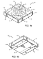
- FIG. 4 a is an upper perspective view of another embodiment of an LED package according to the present invention.
- FIG. 4 b is a bottom perspective view of the LED package shown in FIG. 2 a;
- FIG. 5 is a flow diagram for one embodiment of a fabrication method according to the present invention.
- FIG. 6 a is a sectional view of one embodiment of a lens mold according to the present invention.
- FIG. 6 b is another sectional view of the lens mold shown in FIG. 6 a;
- FIG. 7 a is a plan view of one embodiment of a submount panel with lenses arranged according to the present invention.
- FIG. 7 b is a sectional view of the submount panel taken in FIG. 7 a taken along section lines 7 b - 7 b.
- the present invention is directed to compact, simple and efficient LED packages and methods for manufacturing same.
- Different embodiments can comprise one or more high power LEDs that typically operate at elevated temperatures.
- Packages according to the present invention can include features to provide for improved thermal management by spreading the heat from the LED. The heat can then dissipate into the ambient.
- the packages according to the present invention can also comprise a lens molded directly over the one or more LEDs to protect the LED while still allowing for efficient emission characteristics.
- the present invention is also directed to methods for fabricating LED packages using processing steps that allow for the simultaneous formation of a plurality of packages. This can reduce the manufacturing complexity and cost of LED package fabrication.
- the present invention provides low cost, relatively small size LED packages that provide an efficient but small light source.
- the packages according to the present invention are particularly adapted to surface mount technologies and provide features that allow for the good thermal dissipation, allowing the packages to operate at elevated power levels without overheating.
- first, second, etc. may be used herein to describe various elements, components, regions, layers and/or sections, these elements, components, regions, layers and/or sections should not be limited by these terms. These terms are only used to distinguish one element, component, region, layer or section from another region, layer or section. Thus, a first element, component, region, layer or section discussed below could be termed a second element, component, region, layer or section without departing from the teachings of the present invention.
- Embodiments of the invention are described herein with reference to cross-sectional view illustrations that are schematic illustrations of idealized embodiments of the invention. As such, variations from the shapes of the illustrations as a result, for example, of manufacturing techniques and/or tolerances are expected. Embodiments of the invention should not be construed as limited to the particular shapes of the regions illustrated herein but are to include deviations in shapes that result, for example, from manufacturing. A region illustrated or described as square or rectangular will typically have rounded or curved features due to normal manufacturing tolerances. Thus, the regions illustrated in the figures are schematic in nature and their shapes are not intended to illustrate the precise shape of a region of a device and are not intended to limit the scope of the invention.
- the present invention can be used in with many different solid state emitters with the embodiments of the invention below being described in relation to LEDs, and in particular to white emitting LEDs and LED packages. It is understood that the present invention can also use other solid state emitter packages beyond the embodiment shown. The present invention can also be used with multiple emitter packages, such as LED packages having more than one LED. The present invention can be used in any application wherein a conversion material is used to down-convert the wavelength of light from an emitter, and the discussion of the present invention with reference to the following embodiment should not be construed as limiting to the that particular embodiment or similar embodiments.
- FIGS. 2 a through 2 g show one embodiment of an LED package 30 according to the present invention generally comprising a substrate/submount (“submount”) 32 with one or more LEDs emitting the same or different colors.
- a single LED 34 is mounted on the submount 32 .
- the LED 34 can have many different semiconductor layers arranged in different ways. LED structures and their fabrication and operation are generally known in the art and only briefly discussed herein.
- the layers of the LED 34 can be fabricated using known processes with a suitable process being fabrication using metal organic chemical vapor deposition (MOCVD).
- MOCVD metal organic chemical vapor deposition
- the layers of the LEDs 34 generally comprise an active layer/region sandwiched between first and second oppositely doped epitaxial layers all of which are formed successively on a growth substrate. LEDs can be formed on a wafer and then singulated for mounting in a package. It is understood that the growth substrate can remain as part of the final singulated LED or the growth substrate can be fully or partially removed.
- the active region can comprise single quantum well (SQW), multiple quantum well (MQW), double heterostructure or super lattice structures.
- SQW single quantum well
- MQW multiple quantum well
- the active region and doped layers may be fabricated from different material systems, with preferred material systems being Group-III nitride based material systems.
- Group-III nitrides refer to those semiconductor compounds formed between nitrogen and the elements in the Group III of the periodic table, usually aluminum (Al), gallium (Ga), and indium (In).
- the term also refers to ternary and quaternary compounds such as aluminum gallium nitride (AlGaN) and aluminum indium gallium nitride (AlInGaN).
- the doped layers are gallium nitride (GaN) and the active region is InGaN.
- the doped layers may be AlGaN, aluminum gallium arsenide (AlGaAs) or aluminum gallium indium arsenide phosphide (AlGaInAsP).
- the growth substrate can be made of many materials such at sapphire, silicon carbide, aluminum nitride (AlN), GaN, with a suitable substrate being a 4H polytype of silicon carbide, although other silicon carbide polytypes can also be used including 3C, 6H and 15R polytypes.
- Silicon carbide has certain advantages, such as a closer crystal lattice match to Group III nitrides than sapphire and results in Group III nitride films of higher quality. Silicon carbide also has a very high thermal conductivity so that the total output power of Group-III nitride devices on silicon carbide are typically not limited by the thermal dissipation of the substrate (as may be the case with some devices formed on sapphire).
- SiC substrates are available from Cree Research, Inc., of Durham, N.C. and methods for producing them are set forth in the scientific literature as well as in a U.S. Pat. Nos. Re. 34,861; 4,946,547; and 5,200,022.
- the LED 34 can also comprise a conductive current spreading structure 36 and wire bond pads 38 on its top surface, both of which are made of a conductive material and can be deposited using known methods. Some materials that can be used for these elements include Au, Cu, Ni, In, Al, Ag or combinations thereof and conducting oxides and transparent conducting oxides.
- the current spreading structure 36 generally comprises conductive fingers 37 arranged in a grid on the LED 34 with the fingers spaced to enhance current spreading from the pads 38 into the LED's top surface. In operation, an electrical signal is applied to the pads 38 , such as through a wire bond as described below, and the electrical signal spreads through the fingers 37 of the current spreading structure 36 and the top surface into the LED 34 .
- Current spreading structures are often used in LEDs where the top surface is p-type, but can also be used for n-type materials.
- the LED can be coated with one or more phosphors with the phosphors absorbing at least some of the LED light and emitting a different wavelength of light such that the LED emits a combination of light from the LED and the phosphor. In a preferred embodiment the LED emits a white light combination of LED and phosphor light.
- the LED can be coated and fabricated using many different methods, with one suitable method being described in U.S. patent application Ser. Nos. 11/656,759 and 11/899,790, both entitled “Wafer Level Phosphor Coating Method and Devices Fabricated Utilizing Method”, and both of which are incorporated herein by reference.
- LEDs can be coated using other methods such an electrophoretic deposition (EPD), with a suitable EPD method described in U.S. patent application Ser. No. 11/473,089 entitled “Close Loop Electrophoretic Deposition of Semiconductor Devices”, which is also incorporated herein by reference. It is understood that LED packages according to the present invention can also have multiple LEDs of different colors, one or more of which may be white emitting.
- EPD electrophoretic deposition
- the submount 32 can be formed of many different materials with a preferred material being electrically insulating. Suitable materials include, but are not limited to ceramic materials such as aluminum oxide, aluminum nitride or organic insulators like polyimide (PI) and polyphthalamide (PPA). In other embodiments the submount 32 can comprise a printed circuit board (PCB), sapphire or silicon or any other suitable material, such as T-Clad thermal clad insulated substrate material, available from The Bergquist Company of Chanhassen, Minn. For PCB embodiments different PCB types can be used such as standard FR-4 PCB, metal core PCB, or any other type of printed circuit board.
- PCB printed circuit board
- LED packages according to the present invention can be fabricated using a method that utilizes a submount panel sized to accommodate a plurality of sumbmounts. Multiple LED packages can be formed on the panel, with the individual packages being singulated from the panel.
- the submount 32 has a top surface 40 comprising patterned conductive features that can include a die attach pad 42 with an integral first contact pad 44 .
- a second contact pad 46 is also included on the submount's top surface 40 with the LED 34 mounted approximately at the center of the attach pad 42 .
- These patterned conductive features provide conductive paths for electrical connection to the LED 34 using known contacting methods.
- the LED can be mounted to the attach pad 42 using known methods and material mounting such as using conventional solder materials that may or may not contain a flux material or dispensed polymeric materials that may be thermally and electrically conductive.
- the size of the submount 32 in package 30 can vary depending on different factors, with one being the size of the LED.
- the size of the package 30 can be essentially of the same dimension as the effective heat spreading area in the attach pad, and first and second contact pads 42 , 44 , and 46 .
- the submount In a package having a 1 mm LED, the submount can be approximately 3.5 mm by 3.5 mm; with a package having a 0.7 mm chip it can be 3.2 mm by 3.2 mm and generally of square shape in both cases. It is further understood that the submount can have other shapes including circular, rectangular or other multiple sided shapes.
- the attach pad 42 and first and second contact pads 44 , 46 can comprise much different material such as metals or other conductive materials.
- the pads 42 , 44 , 46 comprise copper deposited using known techniques such as plating. In typical plating process a titanium adhesion layer and copper seed layer are sequentially sputtered onto a substrate. Then, approximately 75 microns of copper is plated onto the copper seed layer. The resulting copper layer being deposited can then be patterned using standard lithographic processes. In other embodiments the layer can be sputtered using a mask to form the desired pattern.
- some of the conductive features can include only copper, with others of the features including additional materials.
- the attach pad 42 can be plated or coated with additional metals or materials to the make the attach pad 42 more suitable for mounting an LED 34 .
- the attach pad 42 can be plated with adhesive or bonding materials, or reflective and barrier layers.
- a gap 48 (best shown in FIGS. 2 a and 2 d ) is included between the second pad 46 and the attach pad 42 down to the surface of the submount 32 that, with the gap providing electrical isolation between the attach pad 42 and second pad 46 .
- an electrical signal is applied to the LED 34 through the second pad 46 and the first pad 44 , with the electrical signal on the first pad 44 passing directly to the LED 34 through the attach pad 42 and the signal from the second pad passing into the LED 34 through wire bonds.
- the gap 48 provides electrical isolation between the second pad 46 and attach pad to prevent shorting of the signal applied to the LED 34 .
- an electrical signal can be applied to the package 30 by providing external electrical contact to the first and second bond pads 44 , 46 such as by solder contacts or other conductive paths to a PCB.
- the LED package 30 is arranged for mounting using surface mount technology and having internal conductive paths.
- the LED 30 comprises first and second surface mount pads 50 , 52 (best shown in FIGS. 2 c and 2 e ) that can be formed on the submount's back surface 54 , at least partially in alignment with the first and second contact pads 44 , 46 , respectfully.
- Conductive vias 56 are formed through the submount 32 between the first mounting pad 50 and the first contact pad 44 , such that when a signal is applied to the first mounting pad 50 is conducted to first contact pad 44 .
- conductive vias 56 are formed between the second mounting pad 52 and second contact pad 46 to conduct an electrical signal between the two.
- the first and second mounting pads 50 , 52 allow for surface mounting of the LED package 30 with the electrical signal to be applied to the LED 34 applied across the first and second mounting pads 50 , 52 .
- the vias 56 and mounting pads 50 , 52 can made of many different materials deposited using different techniques, such as those used for the attach and contact pads 42 , 44 , 46 .
- the mounting pads 50 , 52 and vias 56 can be arranged in many different ways and can have many different shapes and sizes. It is also understood that instead of vias, one or more conductive traces can be provided on the surface of the submount between the mounting pads and contact pads, such as along the side surface of the submount.
- a solder mask 58 made of conventional materials can be included on the submount's top surface 40 , at least partially covering the attach pad 42 and the first and second contact pads 44 , 46 , and at least partially covering the gap 48 .
- the solder mask 58 protects these features during subsequent processing steps and in particular mounting the LED 34 to the attach pad 42 and wire bonding. During these steps there can be a danger of solder or other materials depositing in undesired areas, which can result in damage to the areas or result in electrical shorting.
- the solder mask serves as an insulating and protective material that can reduce or prevent these dangers.
- the solder mask comprises an opening for mounting the LED 34 to the attach pad 42 and for attaching wire bonds to the second contact pad 46 . It also comprises side openings 60 to allow convenient electrical access to the contact pads 44 , 46 for testing the package 30 during fabrication.
- the solder mask 58 also has alignment holes that provide for alignment during fabrication of the package 30 and also allow for alignment when mounted in place by the end user.
- the solder mask can be provided with a symbol or indicator 69 to illustrate which side of the LED package 30 should be coupled to the plus or minus of the signal to be applied to the package. This can ensure accurate mounting of the LED package 30 to a PCB or other fixture, whether by machine or hand.
- the symbol 69 comprises a plus (+) sign over the first contact pad 44 , indicating that the package 30 should be mounted with the positive of the signal coupled to the first mounting pad 50 . The minus of the signal would then be coupled to the second mounting pad 52 . It is understood that many different symbol types can be used and that a symbol can also be included over the second conductive pad 46 . It is also understood that the symbols can be placed in other locations other than the solder mask 58 .
- the package 30 can also comprise elements to protect against damage from electrostatic discharge (ESD).
- ESD electrostatic discharge
- the elements are on-chip, and different elements can be used such as various vertical silicon (Si) Zener diodes, different LEDs arranged in parallel and reverse biased to the LED 34 , surface mount varistors and lateral Si diodes.
- a Zener diode 62 is utilized and is mounted to the attach pad 42 using known mounting techniques. The diode is relatively small so that it does not cover an excessive area on the surface of the submount 32 .
- the solder mask 58 includes and opening for the ESD diode 62 so that it can be mounted to the attach pad 42 .
- Different mounting materials and methods can be used such as those used to mount the LED 34 to the attach pad 42 .
- An ESD wire bond 64 is included between the second contact pad 46 at the solder mask opening and the ESD diode 62 .
- Two LED wire bonds 65 are also included between the solder mask opening in the second contact pad 46 and wire bond pads 38 on the LED 34 . In other embodiments only one wire bond can be included between the LED 34 and second contact pad.
- This LED 34 and ESD diode 62 arrangement allows excessive voltage and/or current passing through the LED package 30 from an ESD event to pass through the diode 62 instead of the LED 34 , protecting the LED 34 from damage.
- the wire bonds 64 and 65 can be applied using known methods and can comprise known conductive materials, with a suitable material being gold (Au). It is understood that in other embodiments of an LED package according to the present invention can be provided without an ESD element/diode or with an ESD element/diode that is external to the LED package 30 .
- heat typically does not spread efficiently into the submount 32 , particularly those made of materials such as ceramic.
- an LED is provided on an attach pad that extends generally only under the LED, heat does not spread through most of the submount, and is generally concentrated to the area just below the LED. This can cause overheating of the LED which can limit the operating power level for the LED package.
- the pads 42 , 44 , 46 provide extending thermally conductive paths to laterally conduct heat away from the LED 34 such that it can spread to other areas of the submount beyond the areas just below the LED 34 .
- the attach pad 42 covers more of the surface of the submount 32 than the LED 34 , with the attach pad extending from the edges of the LED 34 toward the edges of the submount 32 .
- the attach pad 42 is generally circular and extending radially from LED 34 toward the edges of the submount 32 .
- a portion of the attach pad 42 intersects with the first and second contact pads 44 , 46 , with the gap 48 separating part of the attach pad adjacent to the second contact pad 46 . It is understood that the contact pad 42 can be many other shapes and in some embodiments it can extend to the edge of the submount 32 .
- the contact pads 44 , 46 also cover the surface of the submount 32 extending out from the vias, and covering the area between the vias 56 , and the area between the vias 56 and the edges of the submount 32 .
- the pads 42 , 44 , and 46 can cover different percentages of the top surface 40 of the submount 32 , with a typical coverage area being greater than 50%. In the LED package 30 , the pads 42 , 44 and 46 can cover approximately 70% of the submount. In other embodiments the coverage area can be greater than 75%.
- the LED package 30 can further comprise a metalized area 66 on the back surface 54 of the submount, between the first and second mounting pads 50 , 52 .
- the metalized area is preferably made of a heat conductive material and is preferably in at least partial vertical alignment with the LED 34 . In one embodiment, the metalized area is not in electrical contact with the elements on top surface of the submount 32 or the first and second mounting pads on the back surface of the submount 32 . Although heat from the LED is laterally spread over the top surface of the submount by the attach pad 42 and the pads 44 , 46 more heat will pass into the submount 32 directly below and around the LED 34 .
- the metalized area can assist with this dissipation by allowing this heat to spread into the metalized area where it can dissipate more readily. It is also noted that the heat can conduct from the top surface of the submount 32 , through the vias 56 , where the heat can spread into the first and second mounting pads 50 , 52 where it can also dissipate.
- the thickness of the metalized area 66 (best shown in FIGS. 2 c and 2 e ) and the first and second pads 50 , 52 should be approximately the same such that all three make contact to a lateral surface such as a PCB.
- solder dams 67 can be included around the area of the attach pad 42 for mounting of the LED 34 , with the solder dams serving to help center the LED and to reduce movement of the LED from the mounting area during while the mounting solder is in liquid form. When the liquid solder encounters any one of the dams, movement is slowed or stopped. This helps reduce the movement of the LED until the solder hardens.
- An optical element or lens 70 is formed on the top surface 40 of the submount 32 , over the LED 34 , to provide both environmental and/or mechanical protection.
- the lens 70 can be in different locations on the top surface 40 with the lens located as shown with the LED 34 at approximately the center of the lens base.
- the lens can be formed in direct contact with the LED 34 and the submount's top surface 40 .
- the lens 70 can be molded using different molding techniques and the lens can be many different shapes depending on the desired shape of the light output.
- One suitable shape as shown is hemispheric, with some examples of alternative shapes being ellipsoid bullet, flat, hex-shaped and square.
- Many different materials can be used for the lens such as silicones, plastics, epoxies or glass, with a suitable material being compatible with molding processes. Silicone is suitable for molding and provides suitable optical transmission properties. It can also withstand subsequent reflow processes and does not significantly degrade over time. It is understood that the lens 70 can also be textured to improve light extraction or can contain materials such as phosphors or scattering particles.
- the LED package 30 can also comprise a protective layer 74 covering the submount's top surface 40 between the lens 70 and edge of the submount 32 .
- the layer 74 provides additional protection to the elements on the top surface to reduce damage and contamination during subsequent processing steps and use.
- Protective layer 74 can be formed during formation of the lens 70 and can comprise the same material as the lens 70 . It is understood, however, that the LED package 30 can also be provided without the protective layer 74 .
- the lens 70 should also be able to withstand certain sheer forces before being displaced from the submount 32 .
- the lens can withstand a 1 kilogram (kg) or more sheer force.
- the lens can withstand a 1 kilogram (kg) or more sheer force.
- properties such as high adhesion and high tensile strength may also contribute to the ability of the lens to withstand sheer forces.
- the lens arrangement of the LED package 30 is also easily adapted for use with secondary lens or optics that can be includes over the lens by the end user to facilitate beam shaping.
- secondary lenses are generally known in the art, with many of them being commercially available.
- FIGS. 3 a to 3 e show another embodiment of an LED package 100 according to the present invention having similar features to those in LED package 30 .
- the LED package 100 comprises a submount 32 , and LED 34 , a lens 70 and wire bonds 64 and 65 .
- LED package 100 is arranged for surface mounting but has a different arrangement for its conductive pads that provides for contacting at one side of the submount 32 .
- the LED package comprises an attach pad 102 with an integral first contact pad 104 , separated by a gap 108 from a second contact pad 106 .
- a gap 108 provides electrical isolation as described above.
- the LED 34 is mounted to the attach pad using the methods described above, and the wire bond 65 runs between the second contact pad 106 to conduct the electrical signal at the second contact pad 106 to the LED 34 .
- the first and second contact pads 104 , 106 are not on opposite sides of the submount 32 , but are instead on the same side.
- the attach pad 102 covers most of the submount's top surface 40 to provide improved heat spreading as described above.
- the first and second contact pads 104 , 106 also cover portions of the top surface to assist in current spreading.
- First and second surface mount contact 110 , 112 are included on the submount's back surface 54 , at least in partial vertical alignment with the first and second contact pads 104 , 106 , respectively.
- Conductive vias 114 run through the submount between the first surface mount contact 110 and the first contact pad 104 , and the second surface mount contact 112 and the second contact pad 106 , so that an electrical signal on the surface mount contacts 110 , 112 is conducted through the vias to the contact pads 104 , 106 . The signal is then conducted to the LED 34 .
- the LED package 100 also comprises a metalized area 116 to further improve heat spreading from the LED 34 and submount 32 .
- the metalized area 116 is not between the surface mount contacts 110 , 112 but covers an area of the back surface 54 opposite them.
- the LED package 100 as shown does not have a protective layer covering the submount's top surface 40 between the edge of the lens 70 and the edge of the top surface 40 , although such a protective layer can be included in other embodiments.
- the LED package 100 can also be provided with an ESD protection element 62 and solder mask 58 as described above.
- the LED package 100 provides for improved thermal management as in LED package 30 , but allows for surface mount contacting along one side of the submount instead of opposite sides.
- the LED package can also include symbols 118 to assist in alignment by the end user.
- FIGS. 4 a and 4 b show still another embodiment of an LED package 150 according to the present invention generally comprising a submount 32 , LED 34 , first and second contact pads 50 , 52 , vias 56 , ESD diode 62 , wire bonds 64 , 65 , metalized area 66 , lens 70 and protective layer 74 .
- the attach pad is not circular, but in combination with the first contact pad, comprises a rectangular shaped first conductive layer 152 on and covering the majority the submount 32 .
- Vias 56 run between the first layer 152 and the first contact pad 50 on one side of the first layer 152 , with the LED and ESD diode mounted to a attach pad area on the opposing side.
- a second conductive layer 154 covers most of the remainder of the submount's top surface, with a gap 156 between the first and second layers 152 , 154 .
- Vias 56 run between the second layer 154 and the second contact pad 52 , with the wire bonds 64 , 65 running between the second layer 154 and the LED 43 and ESD diode 62 .
- an electrical signal applied to the first and second contact pads 50 , 52 is conducted to the LED 34 , causing it to emit light.
- the first and second layers 152 , 154 cover substantially all of the submount's top surface, providing the capability for broad lateral heat spreading from the LED 34 .
- This arrangement presents a minimal pattern for pattern recognition during assembly.
- the shaped pad arrangement shown in FIGS. 2 a - 2 g provides for greater pattern recognition for assembly, while at the same time providing suitable lateral current spreading.
- FIG. 5 shows one embodiment of an LED package fabrication method 200 according to the present invention.
- a substrate (submount) panel that can be diced in subsequent manufacturing steps to provide a plurality of individual submounts.
- a panel is provided to allow for the simultaneous fabrication of a plurality of packages. It is understood that a separate processing step is required for providing the LED package conductive features on the panel. These features can include the attach pad, contact pads, surface mount pads, vias and metalized area, all of which can be arranged to assist in dissipating heat generated by the LED.
- the panel will comprise a plurality of these features arranged in sets, each of the sets corresponding to one of the plurality of packages to be formed from the panel.
- Many different panel sizes can be used such as for example, 3 inches by 4 inches, 2 inches by 4 inches, and 4 inches by 4 inches.
- a plurality of LEDs are provided, each of which is to be mounted to a respective one of the attach pads on the substrate panel.
- the plurality of LEDs comprise white emitting LEDs chips, and many different white chips can be used with a suitable white chip being described in the patent applications mentioned above and incorporated herein.
- more than one LED can be provided for mounting to each of the attach pads.
- a plurality of ESD protection elements can also be provided, each of which can be mounted in conjunction with one of the attach pads to provide ESD protection for its LED package.
- each of the LEDs is die attached to the one of the attach pads, and as mentioned above, many different mounting methods and materials can be used, with a suitable method being mounting using conventional solder materials and methods.
- each of the ESD elements can also be mounted to a respective attach pad using the same mounting method and material. It is understood that the ESD element can also be mounted in other locations using other methods.
- wire bonds are formed on the for each of the LEDs and ESD elements electrically connecting them to the appropriate one of their respective contact pads. As described above, each of the LEDs and their accompanying ESD element can be wire bonded to the second contact pad.
- the wire bonds can be formed using known processes and can be made of known conductive materials such as gold.
- the LEDs can be provided and mounted to the panel without the desired conversion material.
- the conversion material can be deposited on the LED after wire bonding.
- the conversion material or phosphor is deposited on the LED and many different known phosphor deposition methods can be used such as electrophoretic deposition or EPD. Many different phosphor deposition processes can be used with a suitable EPD process described in the patent application described above.
- a lens is molded over each of the LEDs and many different molding methods can be used.
- a molding process is used that simultaneously forms lenses over the LEDs in the submount panel.
- One such molding process is referred to as compression molding processes.
- FIGS. 6 a and 6 b one embodiment of compression molding is shown wherein a mold 250 is provided having a plurality of cavities 252 each of which has an inverted shape of the lens, wherein each cavity 252 is arranged to align with a respective one of the LEDs 254 on a substrate panel 256 .
- the mold 250 is loaded with a lens material 257 in liquid form filling the cavities 252 , with the preferred material being liquid curable silicone.
- the panel 256 is moved toward the cavity with each of the LEDs 254 being embedded in the liquid silicone within one a respective one of the cavities 252 .
- a layer of silicone can also remain between adjacent lenses that provides a protective layer over the top surface of the submount.
- the liquid silicone can then be cured using known curing processes.
- the panel can then be removed from the mold and as shown in FIGS. 7 a and 7 b the panel can comprise a plurality of lenses 258 , each of which is over a respective one of the LEDs 254 .
- the individual LED packages can then be separated from the panel, such as along dashed lines shown.
- the panel can then diced/singulated to separate the individual LED packages and different methods can be used such as known saw singulation methods.
- a tape can be attached to the panel prior to singulation to hold and stabilize the panel and individual LED packages.
- the LED packages can be cleaned and dried.
- each of the LED packages can be tested to be sure they are operating correctly and to measure each device output light characteristics. It is understood that the packages can also be tested at different points in this method by probing the submount panel.
- the LED packages can be binned according to their output characteristics, packaged according to each bin, and shipped to the customer.
Abstract
Description
Claims (34)
Priority Applications (17)
| Application Number | Priority Date | Filing Date | Title |
|---|---|---|---|
| US11/982,275 US9070850B2 (en) | 2007-10-31 | 2007-10-31 | Light emitting diode package and method for fabricating same |
| US12/154,691 US7821023B2 (en) | 2005-01-10 | 2008-05-23 | Solid state lighting component |
| US12/156,995 US9793247B2 (en) | 2005-01-10 | 2008-06-05 | Solid state lighting component |
| EP08253519.6A EP2056363B1 (en) | 2007-10-31 | 2008-10-29 | Light emitting diode package and method for fabricating same |
| JP2008281533A JP2009111395A (en) | 2007-10-31 | 2008-10-31 | Light emitting diode package and method for fabricating the same |
| US12/757,891 US8866169B2 (en) | 2007-10-31 | 2010-04-09 | LED package with increased feature sizes |
| US12/883,979 US8217412B2 (en) | 2005-01-10 | 2010-09-16 | Solid state lighting component |
| US13/187,232 US10256385B2 (en) | 2007-10-31 | 2011-07-20 | Light emitting die (LED) packages and related methods |
| JP2011259253A JP2012084900A (en) | 2007-10-31 | 2011-11-28 | Light emitting diode package and manufacturing method thereof |
| US13/441,620 US9082921B2 (en) | 2007-10-31 | 2012-04-06 | Multi-die LED package |
| US13/489,035 US8698171B2 (en) | 2005-01-10 | 2012-06-05 | Solid state lighting component |
| JP2012288000A JP2013093604A (en) | 2007-10-31 | 2012-12-28 | Light emitting diode package and method for fabricating the same |
| US13/796,045 US9172012B2 (en) | 2007-10-31 | 2013-03-12 | Multi-chip light emitter packages and related methods |
| US13/796,954 US9666762B2 (en) | 2007-10-31 | 2013-03-12 | Multi-chip light emitter packages and related methods |
| US13/971,547 US9076940B2 (en) | 2005-01-10 | 2013-08-20 | Solid state lighting component |
| US14/705,228 US10892383B2 (en) | 2007-10-31 | 2015-05-06 | Light emitting diode package and method for fabricating same |
| US17/127,154 US11791442B2 (en) | 2007-10-31 | 2020-12-18 | Light emitting diode package and method for fabricating same |
Applications Claiming Priority (1)
| Application Number | Priority Date | Filing Date | Title |
|---|---|---|---|
| US11/982,275 US9070850B2 (en) | 2007-10-31 | 2007-10-31 | Light emitting diode package and method for fabricating same |
Related Parent Applications (3)
| Application Number | Title | Priority Date | Filing Date |
|---|---|---|---|
| US11/743,324 Continuation-In-Part US8125137B2 (en) | 2005-01-10 | 2007-05-02 | Multi-chip light emitting device lamps for providing high-CRI warm white light and light fixtures including the same |
| US12/757,891 Continuation-In-Part US8866169B2 (en) | 2007-10-31 | 2010-04-09 | LED package with increased feature sizes |
| US13/017,502 Continuation-In-Part US9041042B2 (en) | 2007-10-31 | 2011-01-31 | High density multi-chip LED devices |
Related Child Applications (7)
| Application Number | Title | Priority Date | Filing Date |
|---|---|---|---|
| US12/154,691 Continuation-In-Part US7821023B2 (en) | 2005-01-10 | 2008-05-23 | Solid state lighting component |
| US12/156,995 Continuation-In-Part US9793247B2 (en) | 2005-01-10 | 2008-06-05 | Solid state lighting component |
| US12/757,891 Continuation-In-Part US8866169B2 (en) | 2007-10-31 | 2010-04-09 | LED package with increased feature sizes |
| US13/017,502 Continuation-In-Part US9041042B2 (en) | 2007-10-31 | 2011-01-31 | High density multi-chip LED devices |
| US13/187,232 Continuation-In-Part US10256385B2 (en) | 2007-10-31 | 2011-07-20 | Light emitting die (LED) packages and related methods |
| US13/441,620 Continuation-In-Part US9082921B2 (en) | 2007-10-31 | 2012-04-06 | Multi-die LED package |
| US14/705,228 Division US10892383B2 (en) | 2007-10-31 | 2015-05-06 | Light emitting diode package and method for fabricating same |
Publications (2)
| Publication Number | Publication Date |
|---|---|
| US20090108281A1 US20090108281A1 (en) | 2009-04-30 |
| US9070850B2 true US9070850B2 (en) | 2015-06-30 |
Family
ID=40304573
Family Applications (3)
| Application Number | Title | Priority Date | Filing Date |
|---|---|---|---|
| US11/982,275 Active 2029-01-05 US9070850B2 (en) | 2005-01-10 | 2007-10-31 | Light emitting diode package and method for fabricating same |
| US14/705,228 Active US10892383B2 (en) | 2007-10-31 | 2015-05-06 | Light emitting diode package and method for fabricating same |
| US17/127,154 Active US11791442B2 (en) | 2007-10-31 | 2020-12-18 | Light emitting diode package and method for fabricating same |
Family Applications After (2)
| Application Number | Title | Priority Date | Filing Date |
|---|---|---|---|
| US14/705,228 Active US10892383B2 (en) | 2007-10-31 | 2015-05-06 | Light emitting diode package and method for fabricating same |
| US17/127,154 Active US11791442B2 (en) | 2007-10-31 | 2020-12-18 | Light emitting diode package and method for fabricating same |
Country Status (3)
| Country | Link |
|---|---|
| US (3) | US9070850B2 (en) |
| EP (1) | EP2056363B1 (en) |
| JP (3) | JP2009111395A (en) |
Cited By (41)
| Publication number | Priority date | Publication date | Assignee | Title |
|---|---|---|---|---|
| US20130270581A1 (en) * | 2007-10-31 | 2013-10-17 | Cree, Inc. | Multi-chip light emitter packages and related methods |
| US20150271948A1 (en) * | 2012-11-27 | 2015-09-24 | Epcos Ag | Semiconductor Device |
| US9316382B2 (en) | 2013-01-31 | 2016-04-19 | Cree, Inc. | Connector devices, systems, and related methods for connecting light emitting diode (LED) modules |
| US9437788B2 (en) | 2012-12-19 | 2016-09-06 | Cree, Inc. | Light emitting diode (LED) component comprising a phosphor with improved excitation properties |
| WO2017004145A1 (en) | 2015-06-30 | 2017-01-05 | Cree, Inc. | Stabilized quantum dot structure and method of making a stabilized quantum dot structure |
| US20170059120A1 (en) * | 2015-08-28 | 2017-03-02 | Panasonic Intellectual Property Management Co., Ltd. | Led module and light fixture with the same |
| US9691949B2 (en) | 2014-05-30 | 2017-06-27 | Cree, Inc. | Submount based light emitter components and methods |
| US10032971B2 (en) | 2011-09-20 | 2018-07-24 | Lg Innotek Co., Ltd. | Light emitting device package and lighting system including the same |
| US10074635B2 (en) | 2015-07-17 | 2018-09-11 | Cree, Inc. | Solid state light emitter devices and methods |
| US10256385B2 (en) | 2007-10-31 | 2019-04-09 | Cree, Inc. | Light emitting die (LED) packages and related methods |
| WO2019094206A1 (en) | 2017-11-10 | 2019-05-16 | Cree, Inc. | Stabilized quantum dot composite and method of making a stabilized quantum dot composite |
| WO2019094207A1 (en) | 2017-11-10 | 2019-05-16 | Cree, Inc. | Stabilized luminescent nanoparticles comprising perovskite semiconductor and method of fabrication |
| US10453825B2 (en) | 2014-11-11 | 2019-10-22 | Cree, Inc. | Light emitting diode (LED) components and methods |
| WO2019203950A1 (en) | 2018-04-19 | 2019-10-24 | Cree, Inc. | Light-emitting diode package with light-altering material |
| WO2019231817A1 (en) | 2018-05-31 | 2019-12-05 | Cree, Inc. | Stabilized fluoride phosphor for light emitting diode (led) applications |
| US10651351B1 (en) | 2018-11-13 | 2020-05-12 | Cree, Inc. | Light emitting diode packages |
| WO2020131231A1 (en) | 2018-12-17 | 2020-06-25 | Cree, Inc. | Interconnects for light emitting diode chips |
| US10797204B2 (en) | 2014-05-30 | 2020-10-06 | Cree, Inc. | Submount based light emitter components and methods |
| US10957736B2 (en) | 2018-03-12 | 2021-03-23 | Cree, Inc. | Light emitting diode (LED) components and methods |
| WO2021067821A1 (en) | 2019-10-03 | 2021-04-08 | Cree, Inc. | Light emitting diode package with a plurality of lumiphoric regions |
| US10985294B2 (en) | 2019-03-19 | 2021-04-20 | Creeled, Inc. | Contact structures for light emitting diode chips |
| US10991861B2 (en) | 2015-10-01 | 2021-04-27 | Cree, Inc. | Low optical loss flip chip solid state lighting device |
| US11031527B2 (en) | 2018-01-29 | 2021-06-08 | Creeled, Inc. | Reflective layers for light-emitting diodes |
| US11094848B2 (en) | 2019-08-16 | 2021-08-17 | Creeled, Inc. | Light-emitting diode chip structures |
| US11101248B2 (en) * | 2017-08-18 | 2021-08-24 | Creeled, Inc. | Light emitting diodes, components and related methods |
| US11107857B2 (en) * | 2017-08-18 | 2021-08-31 | Creeled, Inc. | Light emitting diodes, components and related methods |
| US11145689B2 (en) * | 2018-11-29 | 2021-10-12 | Creeled, Inc. | Indicia for light emitting diode chips |
| WO2021211648A1 (en) | 2020-04-16 | 2021-10-21 | Creeled, Inc. | Light-altering material arrangements for light-emitting devices |
| US11189766B2 (en) | 2019-01-16 | 2021-11-30 | Creeled, Inc. | Light emitting diode packages |
| WO2022046459A1 (en) | 2020-08-25 | 2022-03-03 | Creeled, Inc. | Binder materials for light-emitting devices |
| WO2022115180A1 (en) | 2020-11-24 | 2022-06-02 | Creeled, Inc. | Cover structure arrangements for light emitting diode packages |
| US11367810B2 (en) | 2020-08-14 | 2022-06-21 | Creeled, Inc. | Light-altering particle arrangements for light-emitting devices |
| WO2022132719A1 (en) | 2020-12-16 | 2022-06-23 | Creeled, Inc. | Light emitting diode packages with support structure |
| US11387389B2 (en) | 2018-01-29 | 2022-07-12 | Creeled, Inc. | Reflective layers for light-emitting diodes |
| WO2022173686A1 (en) | 2021-02-11 | 2022-08-18 | Creeled, Inc. | Light emitting diode package having a cover structure with an optical arrangement, and manufacturing method |
| US20220359802A1 (en) * | 2018-02-26 | 2022-11-10 | Semicon Light Co., Ltd. | Semiconductor light emitting devices and method of manufacturing the same |
| US11508715B2 (en) | 2020-04-24 | 2022-11-22 | Creeled, Inc. | Light-emitting diode chip with electrical overstress protection |
| US11552229B2 (en) | 2020-09-14 | 2023-01-10 | Creeled, Inc. | Spacer layer arrangements for light-emitting diodes |
| USD996377S1 (en) * | 2022-02-17 | 2023-08-22 | Creeled, Inc. | Light-emitting diode package |
| US11791442B2 (en) | 2007-10-31 | 2023-10-17 | Creeled, Inc. | Light emitting diode package and method for fabricating same |
| US11923481B2 (en) | 2018-01-29 | 2024-03-05 | Creeled, Inc. | Reflective layers for light-emitting diodes |
Families Citing this family (111)
| Publication number | Priority date | Publication date | Assignee | Title |
|---|---|---|---|---|
| US7821023B2 (en) * | 2005-01-10 | 2010-10-26 | Cree, Inc. | Solid state lighting component |
| US9793247B2 (en) | 2005-01-10 | 2017-10-17 | Cree, Inc. | Solid state lighting component |
| USD738832S1 (en) | 2006-04-04 | 2015-09-15 | Cree, Inc. | Light emitting diode (LED) package |
| US9780268B2 (en) | 2006-04-04 | 2017-10-03 | Cree, Inc. | Submount based surface mount device (SMD) light emitter components and methods |
| US9335006B2 (en) * | 2006-04-18 | 2016-05-10 | Cree, Inc. | Saturated yellow phosphor converted LED and blue converted red LED |
| US9484499B2 (en) | 2007-04-20 | 2016-11-01 | Cree, Inc. | Transparent ohmic contacts on light emitting diodes with carrier substrates |
| KR101320514B1 (en) * | 2007-08-21 | 2013-10-22 | 삼성전자주식회사 | Light emitting diode package by chip on board |
| US9593810B2 (en) * | 2007-09-20 | 2017-03-14 | Koninklijke Philips N.V. | LED package and method for manufacturing the LED package |
| US9172012B2 (en) | 2007-10-31 | 2015-10-27 | Cree, Inc. | Multi-chip light emitter packages and related methods |
| US8866169B2 (en) * | 2007-10-31 | 2014-10-21 | Cree, Inc. | LED package with increased feature sizes |
| US9082921B2 (en) | 2007-10-31 | 2015-07-14 | Cree, Inc. | Multi-die LED package |
| US8368100B2 (en) | 2007-11-14 | 2013-02-05 | Cree, Inc. | Semiconductor light emitting diodes having reflective structures and methods of fabricating same |
| US9640737B2 (en) | 2011-01-31 | 2017-05-02 | Cree, Inc. | Horizontal light emitting diodes including phosphor particles |
| US9660153B2 (en) | 2007-11-14 | 2017-05-23 | Cree, Inc. | Gap engineering for flip-chip mounted horizontal LEDs |
| US9754926B2 (en) | 2011-01-31 | 2017-09-05 | Cree, Inc. | Light emitting diode (LED) arrays including direct die attach and related assemblies |
| US10008637B2 (en) | 2011-12-06 | 2018-06-26 | Cree, Inc. | Light emitter devices and methods with reduced dimensions and improved light output |
| US9425172B2 (en) | 2008-10-24 | 2016-08-23 | Cree, Inc. | Light emitter array |
| US9255686B2 (en) | 2009-05-29 | 2016-02-09 | Cree, Inc. | Multi-lens LED-array optic system |
| US9035328B2 (en) | 2011-02-04 | 2015-05-19 | Cree, Inc. | Light-emitting diode component |
| US8598809B2 (en) | 2009-08-19 | 2013-12-03 | Cree, Inc. | White light color changing solid state lighting and methods |
| JP5623062B2 (en) | 2009-11-13 | 2014-11-12 | シャープ株式会社 | Light emitting device and manufacturing method thereof |
| US8235549B2 (en) * | 2009-12-09 | 2012-08-07 | Tyco Electronics Corporation | Solid state lighting assembly |
| US8241044B2 (en) * | 2009-12-09 | 2012-08-14 | Tyco Electronics Corporation | LED socket assembly |
| US8845130B2 (en) | 2009-12-09 | 2014-09-30 | Tyco Electronics Corporation | LED socket assembly |
| US8878454B2 (en) | 2009-12-09 | 2014-11-04 | Tyco Electronics Corporation | Solid state lighting system |
| US8210715B2 (en) * | 2009-12-09 | 2012-07-03 | Tyco Electronics Corporation | Socket assembly with a thermal management structure |
| US8511851B2 (en) * | 2009-12-21 | 2013-08-20 | Cree, Inc. | High CRI adjustable color temperature lighting devices |
| JP2011151268A (en) | 2010-01-22 | 2011-08-04 | Sharp Corp | Light-emitting device |
| US8486761B2 (en) * | 2010-03-25 | 2013-07-16 | Koninklijke Philips Electronics N.V. | Hybrid combination of substrate and carrier mounted light emitting devices |
| US8319247B2 (en) | 2010-03-25 | 2012-11-27 | Koninklijke Philips Electronics N.V. | Carrier for a light emitting device |
| US8431942B2 (en) | 2010-05-07 | 2013-04-30 | Koninklijke Philips Electronics N.V. | LED package with a rounded square lens |
| WO2012016377A1 (en) | 2010-08-03 | 2012-02-09 | Industrial Technology Research Institute | Light emitting diode chip, light emitting diode package structure, and method for forming the same |
| US9178107B2 (en) | 2010-08-03 | 2015-11-03 | Industrial Technology Research Institute | Wafer-level light emitting diode structure, light emitting diode chip, and method for forming the same |
| US8956922B2 (en) | 2010-09-06 | 2015-02-17 | Heraeus Noblelight Gmbh | Coating method for an optoelectronic chip-on-board module |
| US9627361B2 (en) * | 2010-10-07 | 2017-04-18 | Cree, Inc. | Multiple configuration light emitting devices and methods |
| DE102010049961A1 (en) * | 2010-10-28 | 2012-05-03 | Osram Opto Semiconductors Gmbh | Optoelectronic semiconductor component with a semiconductor chip, a carrier substrate and a film and a method for its production |
| JP5450559B2 (en) | 2010-11-25 | 2014-03-26 | シャープ株式会社 | LED light source for plant cultivation, plant factory and light emitting device |
| KR101242218B1 (en) * | 2011-01-07 | 2013-03-11 | 에이텍 테크놀로지 코포레이션 | Lighting device and method for forming the same |
| US9053958B2 (en) | 2011-01-31 | 2015-06-09 | Cree, Inc. | Light emitting diode (LED) arrays including direct die attach and related assemblies |
| US9831220B2 (en) | 2011-01-31 | 2017-11-28 | Cree, Inc. | Light emitting diode (LED) arrays including direct die attach and related assemblies |
| US9673363B2 (en) | 2011-01-31 | 2017-06-06 | Cree, Inc. | Reflective mounting substrates for flip-chip mounted horizontal LEDs |
| US9786811B2 (en) | 2011-02-04 | 2017-10-10 | Cree, Inc. | Tilted emission LED array |
| US9401103B2 (en) | 2011-02-04 | 2016-07-26 | Cree, Inc. | LED-array light source with aspect ratio greater than 1 |
| US9245874B2 (en) | 2011-04-18 | 2016-01-26 | Cree, Inc. | LED array having embedded LED and method therefor |
| JP5105132B1 (en) | 2011-06-02 | 2012-12-19 | 三菱化学株式会社 | Semiconductor light emitting device, semiconductor light emitting system, and lighting fixture |
| US8906263B2 (en) | 2011-06-03 | 2014-12-09 | Cree, Inc. | Red nitride phosphors |
| US8729790B2 (en) | 2011-06-03 | 2014-05-20 | Cree, Inc. | Coated phosphors and light emitting devices including the same |
| US8814621B2 (en) | 2011-06-03 | 2014-08-26 | Cree, Inc. | Methods of determining and making red nitride compositions |
| US8747697B2 (en) | 2011-06-07 | 2014-06-10 | Cree, Inc. | Gallium-substituted yttrium aluminum garnet phosphor and light emitting devices including the same |
| USD700584S1 (en) | 2011-07-06 | 2014-03-04 | Cree, Inc. | LED component |
| US10842016B2 (en) | 2011-07-06 | 2020-11-17 | Cree, Inc. | Compact optically efficient solid state light source with integrated thermal management |
| US10686107B2 (en) | 2011-07-21 | 2020-06-16 | Cree, Inc. | Light emitter devices and components with improved chemical resistance and related methods |
| JP2014525146A (en) | 2011-07-21 | 2014-09-25 | クリー インコーポレイテッド | Light emitting device, package, component, and method for improved chemical resistance and related methods |
| US10211380B2 (en) | 2011-07-21 | 2019-02-19 | Cree, Inc. | Light emitting devices and components having improved chemical resistance and related methods |
| US9510413B2 (en) | 2011-07-28 | 2016-11-29 | Cree, Inc. | Solid state lighting apparatus and methods of forming |
| US8742671B2 (en) | 2011-07-28 | 2014-06-03 | Cree, Inc. | Solid state lighting apparatus and methods using integrated driver circuitry |
| US9423119B2 (en) | 2011-09-26 | 2016-08-23 | Ideal Industries, Inc. | Device for securing a source of LED light to a heat sink surface |
| US9429309B2 (en) | 2011-09-26 | 2016-08-30 | Ideal Industries, Inc. | Device for securing a source of LED light to a heat sink surface |
| US9249955B2 (en) | 2011-09-26 | 2016-02-02 | Ideal Industries, Inc. | Device for securing a source of LED light to a heat sink surface |
| KR101896661B1 (en) * | 2011-10-28 | 2018-09-07 | 엘지이노텍 주식회사 | Light emitting device package, back light unit and display unit |
| US10043960B2 (en) * | 2011-11-15 | 2018-08-07 | Cree, Inc. | Light emitting diode (LED) packages and related methods |
| US9496466B2 (en) * | 2011-12-06 | 2016-11-15 | Cree, Inc. | Light emitter devices and methods, utilizing light emitting diodes (LEDs), for improved light extraction |
| US9318669B2 (en) | 2012-01-30 | 2016-04-19 | Cree, Inc. | Methods of determining and making red nitride compositions |
| WO2013116114A1 (en) * | 2012-02-02 | 2013-08-08 | Bridgelux, Inc. | Packaging photon building blocks having only top side connections in a molded interconnect structure |
| US8568001B2 (en) | 2012-02-03 | 2013-10-29 | Tyco Electronics Corporation | LED socket assembly |
| CN104106152A (en) * | 2012-02-10 | 2014-10-15 | 克利公司 | Light emitting devices and packages and related methods with electrode marks on leads |
| US9343441B2 (en) | 2012-02-13 | 2016-05-17 | Cree, Inc. | Light emitter devices having improved light output and related methods |
| US9240530B2 (en) | 2012-02-13 | 2016-01-19 | Cree, Inc. | Light emitter devices having improved chemical and physical resistance and related methods |
| JP2013187400A (en) * | 2012-03-08 | 2013-09-19 | Unistar Opto Corp | Light emitting diode light module having no jumper wire |
| US10222032B2 (en) | 2012-03-30 | 2019-03-05 | Cree, Inc. | Light emitter components and methods having improved electrical contacts |
| US10134961B2 (en) | 2012-03-30 | 2018-11-20 | Cree, Inc. | Submount based surface mount device (SMD) light emitter components and methods |
| US9735198B2 (en) | 2012-03-30 | 2017-08-15 | Cree, Inc. | Substrate based light emitter devices, components, and related methods |
| CN104364904B (en) | 2012-04-06 | 2017-12-08 | 克利公司 | For launching the Light emitting diode component and method of desired beam pattern |
| EP2660644B1 (en) | 2012-05-02 | 2021-12-15 | Rockwell Automation Switzerland GmbH | Lens carrier and optical module for a light curtain and fabrication method |
| US9515055B2 (en) | 2012-05-14 | 2016-12-06 | Cree, Inc. | Light emitting devices including multiple anodes and cathodes |
| US9349929B2 (en) | 2012-05-31 | 2016-05-24 | Cree, Inc. | Light emitter packages, systems, and methods |
| US10439112B2 (en) * | 2012-05-31 | 2019-10-08 | Cree, Inc. | Light emitter packages, systems, and methods having improved performance |
| USD749051S1 (en) * | 2012-05-31 | 2016-02-09 | Cree, Inc. | Light emitting diode (LED) package |
| USD753612S1 (en) * | 2012-09-07 | 2016-04-12 | Cree, Inc. | Light emitter device |
| US9331230B2 (en) * | 2012-10-30 | 2016-05-03 | Cbrite Inc. | LED die dispersal in displays and light panels with preserving neighboring relationship |
| JP6203503B2 (en) * | 2013-02-18 | 2017-09-27 | スタンレー電気株式会社 | Semiconductor light emitting device |
| US8916896B2 (en) * | 2013-02-22 | 2014-12-23 | Cree, Inc. | Light emitter components and methods having improved performance |
| US9219202B2 (en) | 2013-04-19 | 2015-12-22 | Cree, Inc. | Semiconductor light emitting devices including red phosphors that exhibit good color rendering properties and related red phosphors |
| USD735683S1 (en) | 2013-05-03 | 2015-08-04 | Cree, Inc. | LED package |
| EP3016154B1 (en) * | 2013-06-28 | 2020-08-05 | Citizen Watch Co., Ltd. | Led device |
| US9461024B2 (en) | 2013-08-01 | 2016-10-04 | Cree, Inc. | Light emitter devices and methods for light emitting diode (LED) chips |
| USD758976S1 (en) | 2013-08-08 | 2016-06-14 | Cree, Inc. | LED package |
| US10074781B2 (en) | 2013-08-29 | 2018-09-11 | Cree, Inc. | Semiconductor light emitting devices including multiple red phosphors that exhibit good color rendering properties with increased brightness |
| USD746240S1 (en) * | 2013-12-30 | 2015-12-29 | Cree, Inc. | LED package |
| JP6285035B2 (en) * | 2014-01-02 | 2018-02-28 | ティーイー コネクティビティ ネーデルランド ビーヴイTE Connectivity Nederland BV | LED socket assembly |
| USD741821S1 (en) * | 2014-04-10 | 2015-10-27 | Kingbright Electronics Co., Ltd. | LED component |
| US10622522B2 (en) * | 2014-09-05 | 2020-04-14 | Theodore Lowes | LED packages with chips having insulated surfaces |
| USD790486S1 (en) * | 2014-09-30 | 2017-06-27 | Cree, Inc. | LED package with truncated encapsulant |
| DE102014116079A1 (en) * | 2014-11-04 | 2016-05-04 | Osram Opto Semiconductors Gmbh | Optoelectronic component and method for its production |
| USD826871S1 (en) * | 2014-12-11 | 2018-08-28 | Cree, Inc. | Light emitting diode device |
| USD777122S1 (en) * | 2015-02-27 | 2017-01-24 | Cree, Inc. | LED package |
| US11431146B2 (en) | 2015-03-27 | 2022-08-30 | Jabil Inc. | Chip on submount module |
| USD772181S1 (en) * | 2015-04-02 | 2016-11-22 | Genesis Photonics Inc. | Light emitting diode package substrate |
| USD778848S1 (en) * | 2015-04-07 | 2017-02-14 | Cree, Inc. | Solid state light emitter component |
| USD783547S1 (en) * | 2015-06-04 | 2017-04-11 | Cree, Inc. | LED package |
| US9813008B2 (en) * | 2016-04-06 | 2017-11-07 | Lcdrives Corp | Half-bridge switching circuit system |
| JP7253489B2 (en) | 2016-10-24 | 2023-04-06 | インブイティ・インコーポレイテッド | lighting elements |
| US10672957B2 (en) | 2017-07-19 | 2020-06-02 | Cree, Inc. | LED apparatuses and methods for high lumen output density |
| US10546843B2 (en) | 2017-11-03 | 2020-01-28 | Ideal Industries Lighting Llc | White light emitting devices having high luminous efficiency and improved color rendering that include pass-through violet emissions |
| US10541353B2 (en) | 2017-11-10 | 2020-01-21 | Cree, Inc. | Light emitting devices including narrowband converters for outdoor lighting applications |
| JP1618491S (en) * | 2017-11-21 | 2018-11-19 | ||
| JP1628923S (en) * | 2018-04-26 | 2019-04-08 | ||
| CN109860165A (en) * | 2018-12-29 | 2019-06-07 | 广东晶科电子股份有限公司 | A kind of LED component and preparation method thereof |
| US20220077361A1 (en) * | 2019-04-12 | 2022-03-10 | Osram Opto Semiconductors Gmbh | Radiation-Emitting Device and Method for Producing A Plurality of Radiation-Emitting Devices |
| USD926714S1 (en) * | 2019-10-30 | 2021-08-03 | Creeled, Inc. | Light emitting diode package |
| USD1000400S1 (en) * | 2021-04-16 | 2023-10-03 | Creeled, Inc. | Light emitting diode package |
Citations (319)
| Publication number | Priority date | Publication date | Assignee | Title |
|---|---|---|---|---|
| US3760237A (en) | 1972-06-21 | 1973-09-18 | Gen Electric | Solid state lamp assembly having conical light director |
| JPS53118019U (en) | 1977-02-28 | 1978-09-20 | ||
| JPS53126570U (en) | 1977-03-15 | 1978-10-07 | ||
| US4152044A (en) | 1977-06-17 | 1979-05-01 | International Telephone And Telegraph Corporation | Galium aluminum arsenide graded index waveguide |
| US4307297A (en) | 1978-09-12 | 1981-12-22 | U.S. Philips Corporation | Opto-electronic device |
| US4322735A (en) | 1979-05-11 | 1982-03-30 | Tokyo Shibaura Denki Kabushiki Kaisha | Display device |
| JPS5927559A (en) | 1982-08-07 | 1984-02-14 | Mitsubishi Electric Corp | Semiconductor device package |
| JPS5927559Y2 (en) | 1979-06-08 | 1984-08-09 | 才市 岡本 | Vibration isolator |
| US4511425A (en) | 1983-06-13 | 1985-04-16 | Dennison Manufacturing Company | Heated pad decorator |
| JPS6148951A (en) | 1984-08-16 | 1986-03-10 | Toshiba Corp | Semiconductor device |
| JPS6148951U (en) | 1984-08-29 | 1986-04-02 | ||
| US4675575A (en) | 1984-07-13 | 1987-06-23 | E & G Enterprises | Light-emitting diode assemblies and systems therefore |
| JPS62140758U (en) | 1986-02-28 | 1987-09-05 | ||
| JPS62160564U (en) | 1986-03-31 | 1987-10-13 | ||
| JPS6247156Y2 (en) | 1981-07-08 | 1987-12-25 | ||
| FR2586844B1 (en) | 1985-08-27 | 1988-04-29 | Sofrela Sa | SIGNALING DEVICE USING LIGHT EMITTING DIODES. |
| US4946547A (en) | 1989-10-13 | 1990-08-07 | Cree Research, Inc. | Method of preparing silicon carbide surfaces for crystal growth |
| JPH03171780A (en) | 1989-11-30 | 1991-07-25 | Toshiba Lighting & Technol Corp | Light emitting diode display element |
| US5042048A (en) | 1990-03-02 | 1991-08-20 | Meyer Brad E | Target illuminators and systems employing same |
| US5040868A (en) | 1989-05-31 | 1991-08-20 | Siemens Aktiengesellschaft | Surface-mountable opto-component |
| US5122943A (en) | 1991-04-15 | 1992-06-16 | Miles Inc. | Encapsulated light emitting diode and method for encapsulation |
| US5130761A (en) | 1990-07-17 | 1992-07-14 | Kabushiki Kaisha Toshiba | Led array with reflector and printed circuit board |
| US5167556A (en) | 1990-07-03 | 1992-12-01 | Siemens Aktiengesellschaft | Method for manufacturing a light emitting diode display means |
| US5200022A (en) | 1990-10-03 | 1993-04-06 | Cree Research, Inc. | Method of improving mechanically prepared substrate surfaces of alpha silicon carbide for deposition of beta silicon carbide thereon and resulting product |
| JPH06177424A (en) | 1992-12-03 | 1994-06-24 | Rohm Co Ltd | Light emitting diode lamp and assembled light emitting diode display device |
| US5351106A (en) | 1991-07-01 | 1994-09-27 | Amergraph Corporation | Exposure system |
| USRE34861E (en) | 1987-10-26 | 1995-02-14 | North Carolina State University | Sublimation of silicon carbide to produce large, device quality single crystals of silicon carbide |
| JPH07202271A (en) | 1993-12-28 | 1995-08-04 | Matsushita Electric Works Ltd | Light-emitting diode and manufacture thereof |
| JPH07231120A (en) | 1994-02-18 | 1995-08-29 | Rohm Co Ltd | Light emitting device and manufacture thereof and manufacture of led head |
| US5477436A (en) | 1992-08-29 | 1995-12-19 | Robert Bosch Gmbh | Illuminating device for motor vehicles |
| JPH0832120B2 (en) | 1988-05-27 | 1996-03-27 | 松下電器産業株式会社 | Sound field variable device |
| US5703401A (en) | 1995-05-10 | 1997-12-30 | U.S. Philips Corporation | Miniature semiconductor device for surface mounting |
| US5706177A (en) | 1994-12-24 | 1998-01-06 | Temic Telefunken Microelectronic Gmbh | Multi-terminal surface-mounted electronic device |
| JPH10135492A (en) | 1996-10-29 | 1998-05-22 | Citizen Electron Co Ltd | Electronic parts with through hole electrode and its manufacture |
| US5790298A (en) | 1994-05-03 | 1998-08-04 | Gentex Corporation | Method of forming optically transparent seal and seal formed by said method |
| US5813753A (en) | 1997-05-27 | 1998-09-29 | Philips Electronics North America Corporation | UV/blue led-phosphor device with efficient conversion of UV/blues light to visible light |
| JPH10321909A (en) | 1997-05-19 | 1998-12-04 | Nichia Chem Ind Ltd | Semiconductor device |
| JPH118405A (en) | 1997-06-17 | 1999-01-12 | Oki Electric Ind Co Ltd | Light-emitting diode array and light-emitting diode |
| JPH1154802A (en) | 1997-07-30 | 1999-02-26 | Matsushita Electric Ind Co Ltd | Light-emitting diode and display unit manufactured using the same |
| FR2759188B1 (en) | 1997-01-31 | 1999-04-30 | Thery Hindrick | LIGHT SIGNALING DEVICE, PARTICULARLY FOR REGULATING ROAD TRAFFIC |
| US5907151A (en) | 1996-05-24 | 1999-05-25 | Siemens Aktiengesellschaft | Surface mountable optoelectronic transducer and method for its production |
| JPH11150306A (en) | 1997-09-12 | 1999-06-02 | Unisplay Sa | Light source and lamp provided with the same |
| JPH11167805A (en) | 1997-12-05 | 1999-06-22 | Kyocera Corp | Reflex led element mounting multiple chips |
| WO1999031737A1 (en) | 1997-12-15 | 1999-06-24 | Osram Opto Semiconductors Gmbh & Co. Ohg | Surface-mounted optoelectronic component and method for producing same |
| US5942770A (en) | 1997-04-14 | 1999-08-24 | Rohm, Co., Ltd. | Light-emitting diode chip component and a light-emitting device |
| JPH11261113A (en) | 1999-01-14 | 1999-09-24 | Rohm Co Ltd | Surface-mounting luminous equipment |
| US5959316A (en) | 1998-09-01 | 1999-09-28 | Hewlett-Packard Company | Multiple encapsulation of phosphor-LED devices |
| US6061160A (en) | 1996-05-31 | 2000-05-09 | Dowa Mining Co., Ltd. | Component device for optical communication |
| US6066861A (en) | 1996-09-20 | 2000-05-23 | Siemens Aktiengesellschaft | Wavelength-converting casting composition and its use |
| EP1005085A2 (en) | 1998-11-19 | 2000-05-31 | Matsushita Electronics Corporation | Resin-encapsulated electronic device |
| JP2000188358A (en) | 1998-12-22 | 2000-07-04 | Rohm Co Ltd | Semiconductor device |
| JP2000223752A (en) | 1999-01-29 | 2000-08-11 | Nichia Chem Ind Ltd | Optical semiconductor device and its forming method |
| JP2000223751A (en) | 1998-11-25 | 2000-08-11 | Nichia Chem Ind Ltd | Led lamp and display device using the led lamp |
| EP0936682B1 (en) | 1996-07-29 | 2000-08-23 | Nichia Chemical Industries, Ltd. | Light emitting device and display device |
| EP0684648B1 (en) | 1994-05-24 | 2000-09-13 | Sharp Kabushiki Kaisha | Method for producing semiconductor device |
| JP2000261041A (en) | 1999-03-04 | 2000-09-22 | Citizen Electronics Co Ltd | Surface-mounting type light emitting diode and manufacture of the same |
| CN1274906A (en) | 1999-05-24 | 2000-11-29 | 索尼公司 | Two-dimensional display device |
| US6183100B1 (en) | 1997-10-17 | 2001-02-06 | Truck-Lite Co., Inc. | Light emitting diode 360° warning lamp |
| JP2001044506A (en) | 1999-07-26 | 2001-02-16 | Ichikoh Ind Ltd | Fixation structure for light emitting diode |
| US6224216B1 (en) | 2000-02-18 | 2001-05-01 | Infocus Corporation | System and method employing LED light sources for a projection display |
| JP2001168400A (en) | 1999-12-09 | 2001-06-22 | Rohm Co Ltd | Chip type light emitting device with case and its manufacturing method |
| US6259608B1 (en) | 1999-04-05 | 2001-07-10 | Delphi Technologies, Inc. | Conductor pattern for surface mount devices and method therefor |
| US6274924B1 (en) | 1998-11-05 | 2001-08-14 | Lumileds Lighting, U.S. Llc | Surface mountable LED package |
| JP2001237463A (en) | 2000-02-24 | 2001-08-31 | Matsushita Electric Works Ltd | Led module |
| US6296367B1 (en) | 1999-10-15 | 2001-10-02 | Armament Systems And Procedures, Inc. | Rechargeable flashlight with step-up voltage converter and recharger therefor |
| JP2001518692A (en) | 1997-07-29 | 2001-10-16 | オスラム オプト セミコンダクターズ ゲゼルシャフト ミット ベシュレンクテル ハフツング ウント コンパニー オッフェネ ハンデルスゲゼルシャフト | Photoelectric element |
| US6330111B1 (en) | 2000-06-13 | 2001-12-11 | Kenneth J. Myers, Edward Greenberg | Lighting elements including light emitting diodes, microprism sheet, reflector, and diffusing agent |
| US6331915B1 (en) | 2000-06-13 | 2001-12-18 | Kenneth J. Myers | Lighting element including light emitting diodes, microprism sheet, reflector, and diffusing agent |
| JP2002009217A (en) | 2000-06-23 | 2002-01-11 | Fuji Electric Co Ltd | Resin-sealed semiconductor device |
| US20020015013A1 (en) | 2000-06-28 | 2002-02-07 | Larry Ragle | Integrated color LED chip |
| WO2002017405A1 (en) | 2000-08-23 | 2002-02-28 | Osram Opto Semiconductors Gmbh | Optoelectronic component and method for the production thereof, module and device comprising a module of this type |
| EP1187226A1 (en) | 2000-09-01 | 2002-03-13 | Citizen Electronics Co., Ltd. | Surface-mount type light emitting diode and method of manufacturing same |
| US20020030194A1 (en) * | 2000-09-12 | 2002-03-14 | Camras Michael D. | Light emitting diodes with improved light extraction efficiency |
| US6359236B1 (en) | 1992-07-24 | 2002-03-19 | Tessera, Inc. | Mounting component with leads having polymeric strips |
| US20020054495A1 (en) | 2000-09-18 | 2002-05-09 | Koito Manufacturing Co., Ltd. | Vehicle lamp |
| US20020061174A1 (en) | 2000-01-21 | 2002-05-23 | Hans Hurt | Electro-optical data transfer module |
| US20020066905A1 (en) | 2000-06-20 | 2002-06-06 | Bily Wang | Wing-shaped surface mount package for light emitting diodes |
| CN2498694Y (en) | 2001-08-14 | 2002-07-03 | 北京利亚德电子科技有限公司 | Inclined LED image module |
| JP2002223005A (en) | 2001-01-26 | 2002-08-09 | Toyoda Gosei Co Ltd | Light emitting diode and display device |
| US20020123163A1 (en) | 2000-04-24 | 2002-09-05 | Takehiro Fujii | Edge-emitting light-emitting semiconductor device and method of manufacture thereof |
| US6447124B1 (en) | 1996-03-19 | 2002-09-10 | Donnelly Mirrors Limited | Electro-optic rearview mirror system |
| US6454437B1 (en) | 1999-07-28 | 2002-09-24 | William Kelly | Ring lighting |
| US20020163001A1 (en) | 2001-05-04 | 2002-11-07 | Shaddock David Mulford | Surface mount light emitting device package and fabrication method |
| US6480389B1 (en) | 2002-01-04 | 2002-11-12 | Opto Tech Corporation | Heat dissipation structure for solid-state light emitting device package |
| US20020171911A1 (en) | 2001-05-17 | 2002-11-21 | Mamoru Maegawa | Method for adjusting the hue of the light emitted by a light-emitting diode |
| US20020171087A1 (en) | 1999-12-22 | 2002-11-21 | Lumileds Lighting, U.S., Llc | III-nitride light-emitting device with increased light generating capability |
| JP2002374005A (en) | 2001-04-10 | 2002-12-26 | Toshiba Corp | Optical semiconductor device |
| US20020195935A1 (en) | 1999-12-30 | 2002-12-26 | Harald Jager | Surface-mountable light-emitting diode light source and method of producing a light-emitting diode light source |
| US20030015708A1 (en) | 2001-07-23 | 2003-01-23 | Primit Parikh | Gallium nitride based diodes with low forward voltage and low reverse current operation |
| US6517218B2 (en) | 2000-03-31 | 2003-02-11 | Relume Corporation | LED integrated heat sink |
| CN2549313Y (en) | 2002-04-17 | 2003-05-07 | 杨英琪 | Fan lights in hall |
| WO2003044870A1 (en) | 2001-11-22 | 2003-05-30 | Mireille Georges | Light-emitting diode illuminating optical device |
| US20030116769A1 (en) | 2001-12-24 | 2003-06-26 | Samsung Electro-Mechanics Co., Ltd. | Light emission diode package |
| JP2003218405A (en) | 2002-01-22 | 2003-07-31 | Alps Electric Co Ltd | Electronic component mounting structure and mounting method |
| US20030160256A1 (en) | 2000-09-01 | 2003-08-28 | General Electric Company | Plastic packaging of LED arrays |
| US6614058B2 (en) | 2001-07-12 | 2003-09-02 | Highlink Technology Corporation | Light emitting semiconductor device with a surface-mounted and flip-chip package structure |
| US6621210B2 (en) | 2000-07-14 | 2003-09-16 | Sony Corporation | Front plate for field-emission display comprising barriers formed of conductive inorganic material |
| JP2003264267A (en) | 2002-03-08 | 2003-09-19 | Rohm Co Ltd | Semiconductor device using semiconductor chip |
| US6624491B2 (en) | 1998-06-30 | 2003-09-23 | Osram Opto Semiconductors Gmbh & Co. | Diode housing |
| US20030183852A1 (en) | 2002-03-20 | 2003-10-02 | Sharp Kabushiki Kaisha | Light emitting device and manufacturing method thereof |
| JP2003318449A (en) | 2003-05-20 | 2003-11-07 | Sanyo Electric Co Ltd | Led light source and its fabricating method |
| US6657393B2 (en) | 2000-09-18 | 2003-12-02 | Koito Manufacturing Co., Ltd. | Vehicle lamp having light sources with LEDs arranged in two groups |
| WO2004003660A1 (en) | 2002-07-01 | 2004-01-08 | Bård Eker Industrial Design As | Projector |
| US6680490B2 (en) | 2001-06-15 | 2004-01-20 | Toyoda Gosei Co., Ltd. | Light-emitting device |
| JP2004022862A (en) | 2002-06-18 | 2004-01-22 | Rohm Co Ltd | Semiconductor device |
| US20040016938A1 (en) | 1996-03-26 | 2004-01-29 | Bruce Baretz | Solid state white light emitter and display using same |
| US6686609B1 (en) | 2002-10-01 | 2004-02-03 | Ultrastar Limited | Package structure of surface mounting led and method of manufacturing the same |
| JP2004056075A (en) | 2002-05-31 | 2004-02-19 | Stanley Electric Co Ltd | Light-emitting device and method of manufacturing the same |
| US20040037076A1 (en) | 2002-07-17 | 2004-02-26 | Sharp Kabushiki Kaisha | Light emitting diode lamp and light emitting diode display unit |
| US6700136B2 (en) * | 2001-07-30 | 2004-03-02 | General Electric Company | Light emitting device package |
| US20040041222A1 (en) | 2002-09-04 | 2004-03-04 | Loh Ban P. | Power surface mount light emitting die package |
| US6710373B2 (en) | 1999-09-27 | 2004-03-23 | Shih-Yi Wang | Means for mounting photoelectric sensing elements, light emitting diodes, or the like |
| JP2004103775A (en) | 2002-09-09 | 2004-04-02 | Eeshikku Kk | Chip led light emitting body and method for manufacturing the same |
| US6717353B1 (en) | 2002-10-14 | 2004-04-06 | Lumileds Lighting U.S., Llc | Phosphor converted light emitting device |
| JP2004111937A (en) | 2002-08-30 | 2004-04-08 | Nichia Chem Ind Ltd | Light-emitting device |
| WO2004036660A1 (en) | 2002-09-02 | 2004-04-29 | Tco Co., Ltd | A surface mounting type light emitting diode |
| US20040079957A1 (en) | 2002-09-04 | 2004-04-29 | Andrews Peter Scott | Power surface mount light emitting die package |
| WO2003049204A3 (en) | 2001-11-30 | 2004-04-29 | Osram Opto Semiconductors Gmbh | Optoelectronic component |
| US20040080939A1 (en) | 2001-04-23 | 2004-04-29 | Jules Braddell | Illuminator |
| EP1418630A1 (en) | 2002-11-07 | 2004-05-12 | Matsushita Electric Industrial Co., Ltd. | LED lamp |
| US20040090174A1 (en) | 2000-12-28 | 2004-05-13 | Stefan Tasch | Light source comprising a light-emitting element |
| CN2617039Y (en) | 2003-02-21 | 2004-05-19 | 游尚桦 | Sticking LED lead frame |
| JP2004146815A (en) | 2002-09-30 | 2004-05-20 | Sanyo Electric Co Ltd | Light emitting device |
| US6746889B1 (en) | 2001-03-27 | 2004-06-08 | Emcore Corporation | Optoelectronic device with improved light extraction |
| WO2004053933A2 (en) | 2002-12-06 | 2004-06-24 | Cree, Inc. | Composite leadframe led package and method of making the same |
| JP2004200236A (en) | 2002-12-16 | 2004-07-15 | Matsushita Electric Ind Co Ltd | Light-emitting diode display |
| US6765235B2 (en) | 2002-02-27 | 2004-07-20 | Oki Data Corporation | Array of semiconductor elements with paired driving scheme |
| WO2004027882A3 (en) | 2002-09-17 | 2004-07-29 | Osram Opto Semiconductors Gmbh | Leadframe-based housing, surface-mounted optoelectronic component, and production method |
| US6770498B2 (en) | 2002-06-26 | 2004-08-03 | Lingsen Precision Industries, Ltd. | LED package and the process making the same |
| US6774401B2 (en) | 2002-07-12 | 2004-08-10 | Stanley Electric Co., Ltd. | Light emitting diode |
| JP2004228387A (en) | 2003-01-23 | 2004-08-12 | Koha Co Ltd | Light emitting device |
| US6784463B2 (en) | 1997-06-03 | 2004-08-31 | Lumileds Lighting U.S., Llc | III-Phospide and III-Arsenide flip chip light-emitting devices |
| US6791259B1 (en) | 1998-11-30 | 2004-09-14 | General Electric Company | Solid state illumination system containing a light emitting diode, a light scattering material and a luminescent material |
| CN2646873Y (en) | 2003-10-16 | 2004-10-06 | 上海三思科技发展有限公司 | A surface sticking type LED with tilted light axis |
| US20040207313A1 (en) | 2003-04-21 | 2004-10-21 | Sharp Kabushiki Kaisha | LED device and portable telephone, digital camera and LCD apparatus using the same |
| US20040207999A1 (en) | 2003-03-14 | 2004-10-21 | Toyoda Gosei Co., Ltd. | LED package |
| US20040217364A1 (en) | 2003-05-01 | 2004-11-04 | Cree Lighting Company, Inc. | Multiple component solid state white light |
| US20040227149A1 (en) | 2003-04-30 | 2004-11-18 | Cree, Inc. | High powered light emitter packages with compact optics |
| JP2004327955A (en) | 2003-04-09 | 2004-11-18 | Citizen Electronics Co Ltd | Led lamp |
| JP2004335740A (en) | 2003-05-07 | 2004-11-25 | Citizen Electronics Co Ltd | Light emitting diode and its package structure |
| JP2004335880A (en) | 2003-05-09 | 2004-11-25 | Toshiba Lighting & Technology Corp | Light emitting device |
| US20040232435A1 (en) | 2003-02-28 | 2004-11-25 | Osram Opto Semiconductors Gmbh | Optoelectronic device with patterned-metallized package body, method for producing such a device and method for the patterned metallization of a plastic-containing body |
| JP2004342870A (en) | 2003-05-16 | 2004-12-02 | Stanley Electric Co Ltd | Light emitting diode to be driven with large current |
| WO2004044877A3 (en) | 2002-11-11 | 2004-12-02 | Cotco Internat Ltd | A display device and method for making same |
| US20040256706A1 (en) | 2003-06-20 | 2004-12-23 | Shintaro Nakashima | Molded package and semiconductor device using molded package |
| JP2005019838A (en) | 2003-06-27 | 2005-01-20 | Nippon Leiz Co Ltd | Light source device and method for manufacturing the same |
| US20050023548A1 (en) | 2003-07-31 | 2005-02-03 | Bhat Jerome C. | Mount for semiconductor light emitting device |
| CN1581527A (en) | 2003-08-13 | 2005-02-16 | 西铁城电子股份有限公司 | Luminous diode |
| JP2005045199A (en) | 2003-07-25 | 2005-02-17 | Seoul Semiconductor Co Ltd | Chip light emitting diode and its manufacturing method |
| CN1591924A (en) | 2003-07-29 | 2005-03-09 | 西铁城电子股份有限公司 | Surface-mounted LED and light emitting device with same |
| JP2005079167A (en) | 2003-08-28 | 2005-03-24 | Kyocera Corp | Light emitting element housing package and light emitting device |
| US6872585B2 (en) | 2001-09-03 | 2005-03-29 | Toyoda Gosei Co., Ltd. | LED device and manufacturing method thereof |
| US6876149B2 (en) | 2002-01-31 | 2005-04-05 | Citizen Electronics Co., Ltd. | Double-face LED device for an electronic instrument |
| EP1521313A2 (en) | 2003-10-03 | 2005-04-06 | LumiLeds Lighting U.S., LLC | Integrated reflector cup for a light emitting device mount |
| US20050072981A1 (en) | 2002-02-19 | 2005-04-07 | Ryoma Suenaga | Light-emitting device and process for producing thereof |
| US20050077535A1 (en) | 2003-10-08 | 2005-04-14 | Joinscan Electronics Co., Ltd | LED and its manufacturing process |
| US20050093005A1 (en) | 2002-06-28 | 2005-05-05 | Osram Opto Semiconductors Gmbh | Optoelectronic component and method for producing it |
| US20050110033A1 (en) | 1998-07-28 | 2005-05-26 | Paul Heremans | High-efficiency radiating device |
| US20050117320A1 (en) | 2003-11-14 | 2005-06-02 | Hon Hai Precision Industry Co., Ltd. | Light-emitting diode and backlight system using the same |
| EP1538680A2 (en) | 2003-12-03 | 2005-06-08 | Sumitomo Electric Industries, Ltd. | Light emitting device |
| JP2005150624A (en) | 2003-11-19 | 2005-06-09 | Matsushita Electric Ind Co Ltd | Lead frame for semiconductor device and surface light emitting device using it |
| US20050135105A1 (en) | 2003-12-19 | 2005-06-23 | Lumileds Lighting U.S., Llc | LED package assembly |
| US6911678B2 (en) | 2003-05-30 | 2005-06-28 | Stanley Electric Co., Ltd. | Glass-sealed light-emitting diode |
| US6914268B2 (en) | 2003-07-24 | 2005-07-05 | South Epitaxy Corporation | LED device, flip-chip LED package and light reflecting structure |
| US20050152127A1 (en) | 2003-12-19 | 2005-07-14 | Takayuki Kamiya | LED lamp apparatus |
| US20050156187A1 (en) | 2002-03-08 | 2005-07-21 | Shinji Isokawa | Semiconductor device using semiconductor chip |
| US20050173692A1 (en) | 2002-12-27 | 2005-08-11 | Park Young H. | Vertical GaN light emitting diode and method for manufacturing the same |
| JP2005223222A (en) | 2004-02-06 | 2005-08-18 | Toyoda Gosei Co Ltd | Solid element package |
| US20050179041A1 (en) * | 2004-02-18 | 2005-08-18 | Lumileds Lighting U.S., Llc | Illumination system with LEDs |
| US20050179376A1 (en) | 2004-02-13 | 2005-08-18 | Fung Elizabeth C.L. | Light emitting diode display device |
| US6932497B1 (en) | 2003-12-17 | 2005-08-23 | Jean-San Huang | Signal light and rear-view mirror arrangement |
| JP2003324214A5 (en) | 2002-04-30 | 2005-08-25 | ||
| US6940704B2 (en) | 2001-01-24 | 2005-09-06 | Gelcore, Llc | Semiconductor light emitting device |
| US20050199899A1 (en) | 2004-03-11 | 2005-09-15 | Ming-Der Lin | Package array and package unit of flip chip LED |
| JP2005259754A (en) | 2004-03-09 | 2005-09-22 | Korai Kagi Kofun Yugenkoshi | Light emitting diode device capable of preventing electrostatic discharge damage |
| JP2005259972A (en) | 2004-03-11 | 2005-09-22 | Stanley Electric Co Ltd | Surface-mounting led |
| US20050231983A1 (en) | 2002-08-23 | 2005-10-20 | Dahm Jonathan S | Method and apparatus for using light emitting diodes |
| WO2005104247A1 (en) | 2004-04-19 | 2005-11-03 | Matsushita Electric Industrial Co., Ltd. | Method for fabricating led illumination light source and led illumination light source |
| JP2005310935A (en) | 2004-04-20 | 2005-11-04 | Sumitomo Metal Electronics Devices Inc | Storing package for light-emitting element |
| US6964877B2 (en) | 2003-03-28 | 2005-11-15 | Gelcore, Llc | LED power package |
| US20050253130A1 (en) | 2004-03-26 | 2005-11-17 | Koito Manufacturing Co., Ltd. | Light source module and vehicle front lamp |
| US6975011B2 (en) | 1995-09-29 | 2005-12-13 | Osram Gmbh | Optoelectronic semiconductor component having multiple external connections |
| JP2005347401A (en) | 2004-06-01 | 2005-12-15 | Meiko:Kk | Optical element chip component |
| JP2006019557A (en) | 2004-07-02 | 2006-01-19 | Fujikura Ltd | Light emitting device, its mounting method, lighting apparatus and display |
| US6995510B2 (en) | 2001-12-07 | 2006-02-07 | Hitachi Cable, Ltd. | Light-emitting unit and method for producing same as well as lead frame used for producing light-emitting unit |
| WO2006016398A1 (en) | 2004-08-10 | 2006-02-16 | Renesas Technology Corp. | Light emitting device and process for manufacturing the same |
| US7009627B2 (en) | 2001-11-21 | 2006-03-07 | Canon Kabushiki Kaisha | Display apparatus, and image signal processing apparatus and drive control apparatus for the same |
| CN1744335A (en) | 2004-08-31 | 2006-03-08 | 斯坦雷电气株式会社 | Surface mount LED |
| JP2006508537A (en) | 2002-11-29 | 2006-03-09 | オスラム オプト セミコンダクターズ ゲゼルシャフト ミット ベシュレンクテル ハフツング | Optoelectronic element |
| USD517025S1 (en) | 2003-03-17 | 2006-03-14 | Nichia Corporation | Light emitting diode |
| US20060060867A1 (en) | 2004-09-09 | 2006-03-23 | Toyoda Gosei Co., Ltd. | Light emitting device |
| US7021797B2 (en) | 2003-05-13 | 2006-04-04 | Light Prescriptions Innovators, Llc | Optical device for repositioning and redistributing an LED's light |
| JP2006108517A (en) | 2004-10-08 | 2006-04-20 | Citizen Watch Co Ltd | Substrate for led connection, illuminator using thereof, and display device using thereof |
| US20060081862A1 (en) | 2004-10-14 | 2006-04-20 | Chua Janet B Y | Device and method for emitting output light using quantum dots and non-quantum fluorescent material |
| EP1653254A2 (en) | 2004-10-18 | 2006-05-03 | Samsung Electronics Co., Ltd. | Light emitting diode and lens for the same |
| US20060091406A1 (en) | 2004-11-04 | 2006-05-04 | Hiroki Kaneko | Illuminating apparatus, method for fabricating the same and display apparatus using the same |
| JP2006119357A (en) | 2004-10-21 | 2006-05-11 | Koha Co Ltd | Display device |
| WO2006048064A1 (en) | 2004-11-03 | 2006-05-11 | Tridonic Optoelectronics Gmbh | Light-emitting diode arrangement comprising a color-converting material |
| GB2420221A (en) | 2004-11-12 | 2006-05-17 | Unity Opto Technology Co Ltd | Semiconductor light emitting diode package with heat sink |
| US20060105478A1 (en) | 2004-11-12 | 2006-05-18 | Lumileds Lighting U.S., Llc | Bonding an optical element to a light emitting device |
| US20060102917A1 (en) | 2002-06-19 | 2006-05-18 | Toshihiko Oyama | Semiconductor light emitting device, method for producing the same and reflector for semiconductor light emitting device |
| US20060108594A1 (en) | 2004-11-11 | 2006-05-25 | Kazuyuki Iwasaki | LED device and method for manufacturing the same |
| WO2006054228A2 (en) | 2004-11-18 | 2006-05-26 | Koninklijke Philips Electronics N.V. | Illuminator and method for producing such illuminator |
| US7064907B2 (en) | 2003-06-12 | 2006-06-20 | Seiko Epson Corporation | Optical part and its manufacturing method |
| EP1653255A3 (en) | 2004-10-29 | 2006-06-21 | Pentair Water Pool and Spa, Inc. | Selectable beam lens for underwater light |
| US20060131591A1 (en) | 2004-12-16 | 2006-06-22 | Naofumi Sumitani | Light emitting apparatus |
| US20060133044A1 (en) | 2004-12-16 | 2006-06-22 | Seoul Semiconductor Co., Ltd. | Leadframe and packaged light emitting diode |
| JP2006179520A (en) | 2004-12-20 | 2006-07-06 | Nichia Chem Ind Ltd | Semiconductor device |
| CN1801498A (en) | 2005-01-07 | 2006-07-12 | 北京大学 | Method for preparing LED chip with separate crystal grain vertical structure |
| WO2006046981A3 (en) | 2004-10-25 | 2006-07-13 | Cree Inc | Solid metal block semiconductor light emitting device mounting substrates and packages including cavities and heat sinks, and methods of packaging same |
| US20060151809A1 (en) | 2003-06-03 | 2006-07-13 | Rohm Co., Ltd | Optical semiconductor unit |
| US20060158899A1 (en) | 2005-01-17 | 2006-07-20 | Omron Corporation | Luminescent light source and luminescent light source array |
| US7087936B2 (en) | 2003-04-30 | 2006-08-08 | Cree, Inc. | Methods of forming light-emitting devices having an antireflective layer that has a graded index of refraction |
| EP1693904A2 (en) | 2005-02-18 | 2006-08-23 | Nichia Corporation | Light emitting device provided with lens for controlling light distribution characteristic |
| JP2006253689A (en) | 2005-03-08 | 2006-09-21 | Avago Technologies General Ip (Singapore) Private Ltd | Packaging of led with high performance for heat dissipation |
| US20060220046A1 (en) | 2005-03-04 | 2006-10-05 | Chuan-Pei Yu | Led |
| US7119422B2 (en) | 2004-11-15 | 2006-10-10 | Unity Opto Technology Co., Ltd. | Solid-state semiconductor light emitting device |
| JP2006324331A (en) | 2005-05-17 | 2006-11-30 | Sony Corp | Light emitting diode and its manufacturing method, integrated light emitting diode and its manufacturing method, growing method of nitride- based group iii-v compound semiconductor, nitride-based group iii-v compound semiconductor growing substrate, light emitting diode backlight, light emitting diode lighting apparatus, light emitting diode display, and electronic equipment |
| US20060267042A1 (en) | 2001-10-12 | 2006-11-30 | Nichia Corporation | Light emitting apparatus and method of manufacturing the same |
| JP2006324589A (en) | 2005-05-20 | 2006-11-30 | Sharp Corp | Led device and manufacturing method thereof |
| CN1874011A (en) | 2005-06-03 | 2006-12-06 | 邢陈震仑 | LED device |
| JP2006332234A (en) | 2005-05-25 | 2006-12-07 | Hitachi Aic Inc | Led device having reflecting function |
| US20060278882A1 (en) | 2005-06-10 | 2006-12-14 | Cree, Inc. | Power lamp package |
| JP2006344692A (en) | 2005-06-07 | 2006-12-21 | Fujikura Ltd | Substrate for mounting light-emitting element and light-emitting element module |
| WO2006135502A1 (en) | 2005-06-10 | 2006-12-21 | Cree, Inc. | High power solid-state lamp |
| US20060291185A1 (en) | 2005-06-28 | 2006-12-28 | Sato Atsushi | Planar light source device and display using the same |
| US7161189B2 (en) | 2004-06-04 | 2007-01-09 | Lite-On Technology Corporation | LED package including a frame |
| CN1913135A (en) | 2005-08-11 | 2007-02-14 | 安华高科技Ecbuip(新加坡)私人有限公司 | PLCC package with integrated lens and method for making the package |
| US20070046176A1 (en) | 2005-04-27 | 2007-03-01 | Spudnik,Inc. | Phosphor Compositions For Scanning Beam Displays |
| US7187009B2 (en) | 2001-06-12 | 2007-03-06 | Citizen Electronics Co., Ltd. | Light emitting diode device for illumination objects |
| EP1187228A4 (en) | 2000-02-09 | 2007-03-07 | Nippon Leiz Corp | Light source |
| JP2007094088A (en) | 2005-09-29 | 2007-04-12 | Matsushita Electric Ind Co Ltd | Display device |
| JP2007109836A (en) | 2005-10-13 | 2007-04-26 | Fuji Electric Holdings Co Ltd | Printed wiring board |
| US20070096139A1 (en) | 2005-11-02 | 2007-05-03 | 3M Innovative Properties Company | Light emitting diode encapsulation shape control |
| US20070109779A1 (en) | 2005-11-11 | 2007-05-17 | Yoshifumi Sekiguchi | Illuminating device and liquid-crystal display device using the same |
| US7224000B2 (en) | 2002-08-30 | 2007-05-29 | Lumination, Llc | Light emitting diode component |
| CN1977399A (en) | 2005-04-01 | 2007-06-06 | 松下电器产业株式会社 | LED component and method for manufacturing same |
| JP2007165840A (en) | 2005-09-09 | 2007-06-28 | Matsushita Electric Works Ltd | Light-emitting device |
| JP2007165029A (en) | 2005-12-12 | 2007-06-28 | Hitachi Displays Ltd | Display device |
| US20070145401A1 (en) | 2005-12-27 | 2007-06-28 | Sharp Kabushiki Kaisha | Semiconductor light emitting device, semiconductor element, and method for fabricating the semiconductor light emitting device |
| JP2007184542A (en) | 2005-12-09 | 2007-07-19 | Matsushita Electric Ind Co Ltd | Light-emitting module, manufacturing method thereof, and backlight apparatus using same |
| CN101005109A (en) | 2006-01-16 | 2007-07-25 | 榎本股份有限公司 | Low height lead frame for LED device and the manufacturing method thereof |
| US20070170449A1 (en) | 2006-01-24 | 2007-07-26 | Munisamy Anandan | Color sensor integrated light emitting diode for LED backlight |
| WO2007083408A1 (en) | 2006-01-20 | 2007-07-26 | Sharp Kabushiki Kaisha | Light source unit, lighting apparatus using the light source unit, and display using the lighting apparatus |
| CN101013689A (en) | 2007-01-30 | 2007-08-08 | 深圳市共达光电器件有限公司 | LED packaging structure and packaging method |
| JP2007243226A (en) | 2007-06-20 | 2007-09-20 | Sony Corp | Light source apparatus and display apparatus |
| WO2007005844A3 (en) | 2005-07-05 | 2007-10-04 | Int Rectifier Corp | Schottky diode with improved surge capability |
| US7282740B2 (en) | 2003-12-17 | 2007-10-16 | Sharp Kabushiki Kaisha | Semiconductor light emitting device |
| US20070241357A1 (en) * | 2004-10-29 | 2007-10-18 | Ledengin, Inc. | LED packages with mushroom shaped lenses and methods of manufacturing LED light-emitting devices |
| JP2007273763A (en) | 2006-03-31 | 2007-10-18 | Sony Corp | Semiconductor device and its manufacturing method |
| US7285802B2 (en) | 2004-12-21 | 2007-10-23 | 3M Innovative Properties Company | Illumination assembly and method of making same |
| WO2007121486A2 (en) | 2006-04-18 | 2007-10-25 | Lamina Lighting, Inc. | Optical devices for controlled color mixing |
| JP2007281323A (en) | 2006-04-11 | 2007-10-25 | Toyoda Gosei Co Ltd | Led device |
| WO2007122516A2 (en) | 2006-04-26 | 2007-11-01 | Cree Hong Kong Limited | Apparatus and method for use in mounting electronic elements |
| JP2007287981A (en) | 2006-04-18 | 2007-11-01 | Konica Minolta Opto Inc | Light emitting device |
| US20070262328A1 (en) | 2006-05-10 | 2007-11-15 | Nichia Corporation | Semiconductor light emitting device and a method for producing the same |
| JP2007299905A (en) | 2006-04-28 | 2007-11-15 | Nichia Chem Ind Ltd | Semiconductor device |
| US20070269586A1 (en) | 2006-05-17 | 2007-11-22 | 3M Innovative Properties Company | Method of making light emitting device with silicon-containing composition |
| US7303315B2 (en) | 2004-11-05 | 2007-12-04 | 3M Innovative Properties Company | Illumination assembly using circuitized strips |
| JP2007317896A (en) | 2006-05-26 | 2007-12-06 | Nichia Chem Ind Ltd | Light emitting diode |
| JP2007329516A (en) | 2007-09-14 | 2007-12-20 | Sharp Corp | Semiconductor light-emitting apparatus |
| US20070295975A1 (en) | 2004-06-25 | 2007-12-27 | Sanyo Electric Co., Ltd. | Light-Emitting Device |
| US20070294975A1 (en) | 2006-06-22 | 2007-12-27 | Paul Nadar | Support panel for removable brackets and the like |
| WO2007127029A3 (en) | 2006-04-24 | 2008-01-17 | Cree Inc | Side-view surface mount white led |
| US20080013319A1 (en) | 2006-07-13 | 2008-01-17 | Everlight Electronics Co., Ltd. | Light emitting diode package |
| US20080026498A1 (en) | 2006-07-31 | 2008-01-31 | Eric Tarsa | Light emitting diode package element with internal meniscus for bubble free lens placement |
| US20080036364A1 (en) | 2006-08-10 | 2008-02-14 | Intematix Corporation | Two-phase yellow phosphor with self-adjusting emission wavelength |
| DE202007012162U1 (en) | 2007-06-05 | 2008-03-20 | Seoul Semiconductor Co., Ltd. | LED housing |
| US20080093606A1 (en) | 2006-10-24 | 2008-04-24 | Chipmos Technologies Inc. | Light emitting chip package and manufacturing method thereof |
| US20080121921A1 (en) | 2006-07-13 | 2008-05-29 | Cree, Inc. | Leadframe-based packages for solid state light emitting devices and methods of forming leadframe-based packages for solid state light emitting devices |
| US20080149960A1 (en) | 2006-12-26 | 2008-06-26 | Nichia Corporation | Light-emitting apparatus and method of producing the same |
| USD572210S1 (en) | 2006-11-01 | 2008-07-01 | Lg Innotek Co., Ltd. | Light-emitting diode (LED) |
| USD572670S1 (en) | 2006-03-30 | 2008-07-08 | Nichia Corporation | Light emitting diode |
| WO2008081794A1 (en) | 2006-12-28 | 2008-07-10 | Nichia Corporation | Light emitting device and method for manufacturing the same |
| WO2008082098A1 (en) | 2006-12-28 | 2008-07-10 | Seoul Semiconductor Co., Ltd. | Light emitting diode package |
| US20080170391A1 (en) | 2007-01-12 | 2008-07-17 | Aizar Abdul Karim Norfidathul | Multi-chip Packaged LED Light Source |
| EP1953834A1 (en) | 2005-11-21 | 2008-08-06 | Matsushita Electric Works, Ltd. | Light-emitting device |
| US20080191232A1 (en) | 2005-08-01 | 2008-08-14 | Seoul Semiconductor Co., Ltd. | Light Emitting Device With A Lens Of Silicone |
| US20080191610A1 (en) | 2004-04-27 | 2008-08-14 | Matsushita Electric Industrial Co., Ltd. | Phosphor composition and method for producing the same, and light-emitting device using the same |
| US20080198594A1 (en) | 2006-12-19 | 2008-08-21 | Lee Sungkeun | Optical module |
| USD576574S1 (en) | 2007-07-17 | 2008-09-09 | Rohm Co., Ltd. | Light emitting diode module |
| US20080230790A1 (en) | 2007-03-23 | 2008-09-25 | Sharp Kabushiki Kaisha | Semiconductor light emitting device |
| US20080258156A1 (en) | 2006-09-29 | 2008-10-23 | Sanyo Electric Co., Ltd. | Light-emitting diode apparatus |
| US20080296590A1 (en) | 2007-05-31 | 2008-12-04 | Kee Yean Ng | LED-Based Light Source Having Improved Thermal Dissipation |
| US20080303052A1 (en) | 2004-09-10 | 2008-12-11 | Seoul Semiconductor Co., Ltd. | Light emitting diode package having multiple molding resins |
| US20080308825A1 (en) | 2007-06-14 | 2008-12-18 | Cree, Inc. | Encapsulant with scatterer to tailor spatial emission pattern and color uniformity in light emitting diodes |
| CN101360368A (en) | 2007-07-30 | 2009-02-04 | 深圳莱特光电有限公司 | Silver layer insulation method in warm white light LED encapsulation process |
| US20090050908A1 (en) | 2005-01-10 | 2009-02-26 | Cree, Inc. | Solid state lighting component |
| US20090050911A1 (en) | 2007-08-24 | 2009-02-26 | Cree, Inc. | Light emitting device packages using light scattering particles of different size |
| US20090057699A1 (en) | 2007-09-04 | 2009-03-05 | Philips Lumileds Lighting Company, Llc | LED with Particles in Encapsulant for Increased Light Extraction and Non-Yellow Off-State Color |
| US20090057708A1 (en) | 2007-08-27 | 2009-03-05 | Norfidathul Aizar Abdul Karim | LED Light Source Having Improved Resistance to Thermal Cycling |
| US20090072251A1 (en) | 2007-09-14 | 2009-03-19 | Cotco Luminant Device Limited | LED surface-mount device and LED display incorporating such device |
| US20090095966A1 (en) | 2007-10-10 | 2009-04-16 | Cree, Inc. | Multiple conversion material light emitting diode package and method of fabricating same |
| US20090129085A1 (en) | 2007-11-16 | 2009-05-21 | Avago Technologies Ecbu Ip (Singapore) Pte. Ltd. | Optical device |
| WO2009074919A1 (en) | 2007-12-11 | 2009-06-18 | Koninklijke Philips Electronics N.V. | Side emitting device with hybrid top reflector |
| US20090189178A1 (en) | 2006-06-30 | 2009-07-30 | Do Hyung Kim | Leadframe having a heat sink supporting part, fabricating method of a light emitting diode package using the same, and light emitting diode package fabricated by the method |
| US7579628B2 (en) | 2004-10-18 | 2009-08-25 | Sharp Kabushiki Kaisha | Backlight device for liquid crystal display including a plurality of light emitting diodes within their own concaves aligned in a straight line within a larger concave |
| GB2458972A (en) | 2008-08-05 | 2009-10-07 | Photonstar Led Ltd | Thermally optimized chip-on-board module |
| US20090283781A1 (en) | 2008-05-16 | 2009-11-19 | Cree Hong Kong Limited | Mini V SMD |
| US7622795B2 (en) | 2007-05-15 | 2009-11-24 | Nichepac Technology Inc. | Light emitting diode package |
| WO2010005294A1 (en) | 2008-06-15 | 2010-01-14 | Stichting Administratiekantoor Vomgroup | A method for manufacturing a lens to be added to a led, and a lens obtained with that method |
| US20100044735A1 (en) | 2008-08-25 | 2010-02-25 | Citizen Electronics Co., Ltd. | Light-emitting device |
| US20100103660A1 (en) | 2008-10-24 | 2010-04-29 | Cree Led Lighting Solutions, Inc. | Array layout for color mixing |
| EP1864780B1 (en) | 2006-06-09 | 2010-05-26 | LG Electronics Inc. | Apparatus and method for manufacturing a light emitting unit |
| GB2466633A (en) | 2008-12-12 | 2010-07-07 | Glory Science Co Ltd | Method of manufacturing a light emitting unit |
| US20100193822A1 (en) | 2009-01-30 | 2010-08-05 | Nichia Corporation | Light emitting semiconductor device and method of manufacture thereof |
| US7777412B2 (en) | 2007-03-22 | 2010-08-17 | Avago Technologies Ecbu Ip (Singapore) Pte. Ltd. | Phosphor converted LED with improved uniformity and having lower phosphor requirements |
| US7875899B2 (en) | 2007-01-15 | 2011-01-25 | Showa Denko K.K. | Light-emitting diode package and lead group structure for light-emitting diode package |
| US20110049545A1 (en) | 2009-09-02 | 2011-03-03 | Koninklijke Philips Electronics N.V. | Led package with phosphor plate and reflective substrate |
| US20110108874A1 (en) | 2009-11-05 | 2011-05-12 | Luminit, Llc | Method to Provide Microstructure for Encapsulated Hgh-Brightness LED Chips |
| US20110186880A1 (en) | 2007-08-30 | 2011-08-04 | Osram Opto Semiconductors Gmbh | LED Housing |
| US20110193118A1 (en) | 2010-02-09 | 2011-08-11 | Oshima Yukitoyo | Light emitting device and manufacturing method thereof |
| US20110278617A1 (en) | 2010-05-12 | 2011-11-17 | Lee Gun Kyo | Light emitting device package |
| EP1349202B1 (en) | 2002-03-28 | 2012-05-02 | Rohm Co., Ltd. | Semiconductor device and method of manufacturing the same |
| US8217414B2 (en) | 2006-12-28 | 2012-07-10 | Nichia Corporation | Light emitting device, package, light emitting device manufacturing method, package manufacturing method and package manufacturing die |
| WO2012099145A1 (en) | 2011-01-20 | 2012-07-26 | シャープ株式会社 | Light emitting device, lighting device, display device, and method for manufacturing light emitting device |
| US20120257386A1 (en) | 2011-06-24 | 2012-10-11 | Xicato, Inc. | Led based illumination module with a reflective mask |
| US20120268957A1 (en) | 2010-10-19 | 2012-10-25 | Philip Premysler | Reflow solderable, surface mount optic mounting |
| US20130056774A1 (en) | 2011-09-02 | 2013-03-07 | Phostek, Inc. | Lens, package and packaging method for semiconductor light-emitting device |
Family Cites Families (328)
| Publication number | Priority date | Publication date | Assignee | Title |
|---|---|---|---|---|
| US473089A (en) | 1892-04-19 | Charles e | ||
| US656759A (en) | 1899-12-11 | 1900-08-28 | Reuben D Wirt | Automatic hose-valve. |
| US2002111A (en) | 1933-08-25 | 1935-05-21 | Edmund H Hansen | System for synchronizing sound with motion pictures |
| US3008676A (en) | 1957-07-30 | 1961-11-14 | Manganese Steel Forge Company | Wire fabric |
| US3011818A (en) | 1959-04-24 | 1961-12-05 | Roy A Matthiessen | Automobile trunk lid holder |
| US3674990A (en) | 1970-05-12 | 1972-07-04 | Sumitomo Electric Industries | Moving object identification system |
| DE2315709A1 (en) | 1973-03-29 | 1974-10-10 | Licentia Gmbh | RADIATION-EMISSING SEMI-CONDUCTOR ARRANGEMENT WITH HIGH RADIATION POWER |
| US3900863A (en) | 1974-05-13 | 1975-08-19 | Westinghouse Electric Corp | Light-emitting diode which generates light in three dimensions |
| JPS5932039B2 (en) | 1977-03-24 | 1984-08-06 | 松下電器産業株式会社 | Polymer piezoelectric transducer |
| JPS53126570A (en) | 1977-04-13 | 1978-11-04 | Saburou Sakakibara | Mechanism for opening and closing filter medium in filter press |
| JPS5479985A (en) | 1977-12-09 | 1979-06-26 | Tokyo Shibaura Electric Co | Ultrasonic scanning device |
| JPS5927559B2 (en) | 1980-05-14 | 1984-07-06 | 株式会社村田製作所 | electroacoustic transformer |
| US4500914A (en) | 1981-08-01 | 1985-02-19 | Sharp Kabushiki Kaisha | Color imaging array and color imaging device |
| JPS58123066U (en) | 1982-02-15 | 1983-08-22 | 小林記録紙株式会社 | Recording paper for measurement |
| US5184114A (en) | 1982-11-04 | 1993-02-02 | Integrated Systems Engineering, Inc. | Solid state color display system and light emitting diode pixels therefor |
| JPS6247156A (en) | 1985-08-26 | 1987-02-28 | Toshiba Corp | Insulated gate type semiconductor device |
| JPS62140758A (en) | 1985-12-16 | 1987-06-24 | Kobe Steel Ltd | Mechanical wire cut saw |
| JPS62160564A (en) | 1986-01-09 | 1987-07-16 | Fujitsu Ltd | Pipeline control system |
| US4972089A (en) | 1989-04-03 | 1990-11-20 | Motorola Inc. | Single package electro-optic transmitter-receiver |
| US4992704A (en) | 1989-04-17 | 1991-02-12 | Basic Electronics, Inc. | Variable color light emitting diode |
| JP2650236B2 (en) | 1990-01-11 | 1997-09-03 | ローム 株式会社 | Manufacturing method of LED array light source |
| US5300788A (en) | 1991-01-18 | 1994-04-05 | Kopin Corporation | Light emitting diode bars and arrays and method of making same |
| JPH05308107A (en) | 1991-07-01 | 1993-11-19 | Sumitomo Electric Ind Ltd | Semiconductor device and its manufacture |
| JPH0545812A (en) | 1991-08-16 | 1993-02-26 | Konica Corp | Silver halide color photographic sensitive material |
| US5278432A (en) | 1992-08-27 | 1994-01-11 | Quantam Devices, Inc. | Apparatus for providing radiant energy |
| JP2783093B2 (en) | 1992-10-21 | 1998-08-06 | 日本電気株式会社 | Printed wiring board |
| JP3341347B2 (en) | 1993-04-07 | 2002-11-05 | 日産自動車株式会社 | Control device for vehicle seat |
| US5454437A (en) | 1993-06-24 | 1995-10-03 | Rock Bit International, Inc. | Roller cone core bit |
| JPH0832120A (en) | 1994-07-19 | 1996-02-02 | Rohm Co Ltd | Surface emission type display |
| JPH08139257A (en) | 1994-11-07 | 1996-05-31 | Hitachi Ltd | Surface mount semiconductor device |
| JPH08322573A (en) | 1995-05-31 | 1996-12-10 | Seikagaku Kogyo Co Ltd | Dna coding for sulfotransferase |
| JP3410256B2 (en) | 1995-06-22 | 2003-05-26 | 日本信号株式会社 | Train position detection device |
| JPH09246602A (en) | 1996-03-05 | 1997-09-19 | Matsushita Electron Corp | Light emitting diode array light source |
| US6388272B1 (en) | 1996-03-07 | 2002-05-14 | Caldus Semiconductor, Inc. | W/WC/TAC ohmic and rectifying contacts on SiC |
| JPH1012915A (en) | 1996-06-26 | 1998-01-16 | Oki Electric Ind Co Ltd | Optical pattern read sensor |
| JP3504079B2 (en) | 1996-08-31 | 2004-03-08 | 株式会社東芝 | Method for manufacturing semiconductor light emitting diode device |
| JP3492178B2 (en) | 1997-01-15 | 2004-02-03 | 株式会社東芝 | Semiconductor light emitting device and method of manufacturing the same |
| JPH10244706A (en) | 1997-03-06 | 1998-09-14 | Oki Data:Kk | Led head |
| US6399358B1 (en) | 1997-03-31 | 2002-06-04 | Thomas Jefferson University | Human gene encoding human chondroitin 6-sulfotransferase |
| US6093940A (en) | 1997-04-14 | 2000-07-25 | Rohm Co., Ltd. | Light-emitting diode chip component and a light-emitting device |
| DE19723176C1 (en) | 1997-06-03 | 1998-08-27 | Daimler Benz Ag | Semiconductor device with alternate p-n and Schottky junctions |
| US7635687B2 (en) * | 1997-06-04 | 2009-12-22 | Oxford Biomedica (Uk) Limited | Vector system |
| JPH1054802A (en) | 1997-06-17 | 1998-02-24 | Nec Corp | Monitoring method for liquid-medicine composition |
| JP3585097B2 (en) | 1998-06-04 | 2004-11-04 | セイコーエプソン株式会社 | Light source device, optical device and liquid crystal display device |
| US6266476B1 (en) | 1998-08-25 | 2001-07-24 | Physical Optics Corporation | Optical element having an integral surface diffuser |
| US7066628B2 (en) | 2001-03-29 | 2006-06-27 | Fiber Optic Designs, Inc. | Jacketed LED assemblies and light strings containing same |
| DE19848078C2 (en) | 1998-10-19 | 2003-08-14 | Insta Elektro Gmbh | Arrangement of boards for the creation of light-emitting diode units |
| US6495964B1 (en) | 1998-12-18 | 2002-12-17 | Koninklijke Philips Electronics N.V. | LED luminaire with electrically adjusted color balance using photodetector |
| JP2000349348A (en) | 1999-03-31 | 2000-12-15 | Toyoda Gosei Co Ltd | Short wavelength led lamp unit |
| JP4412787B2 (en) | 1999-06-09 | 2010-02-10 | 三洋電機株式会社 | Irradiation device and irradiation module using metal substrate |
| JP2001000043A (en) | 1999-06-18 | 2001-01-09 | Mitsubishi Chemicals Corp | Light source for cultivation |
| US6344520B1 (en) | 1999-06-24 | 2002-02-05 | Wacker Silicones Corporation | Addition-crosslinkable epoxy-functional organopolysiloxane polymer and coating compositions |
| US6367949B1 (en) | 1999-08-04 | 2002-04-09 | 911 Emergency Products, Inc. | Par 36 LED utility lamp |
| JP2001050072A (en) | 1999-08-06 | 2001-02-23 | Kokusan Denki Co Ltd | Control system for two-cycle internal combustion engine |
| JP2001060072A (en) | 1999-08-23 | 2001-03-06 | Matsushita Electric Ind Co Ltd | Display device |
| TW526701B (en) | 1999-08-26 | 2003-04-01 | Rohm Co Ltd | Electromagnetic shield cap and infrared data communication module |
| US6573537B1 (en) | 1999-12-22 | 2003-06-03 | Lumileds Lighting, U.S., Llc | Highly reflective ohmic contacts to III-nitride flip-chip LEDs |
| US6885035B2 (en) | 1999-12-22 | 2005-04-26 | Lumileds Lighting U.S., Llc | Multi-chip semiconductor LED assembly |
| GB2370992B (en) | 2000-03-23 | 2002-11-20 | Photo Therapeutics Ltd | Therapeutic light source and method |
| WO2001075954A1 (en) | 2000-03-31 | 2001-10-11 | Toyoda Gosei Co., Ltd. | Method for dicing semiconductor wafer into chips |
| US6661029B1 (en) | 2000-03-31 | 2003-12-09 | General Electric Company | Color tunable organic electroluminescent light source |
| JP2001351404A (en) | 2000-04-06 | 2001-12-21 | Kansai Tlo Kk | Surface emitting device using light-emitting diode |
| JP2001326390A (en) | 2000-05-18 | 2001-11-22 | Rohm Co Ltd | Rear-surface light-emitting chip type light-emitting element and insulating board used therefor |
| US6577073B2 (en) | 2000-05-31 | 2003-06-10 | Matsushita Electric Industrial Co., Ltd. | Led lamp |
| JP2002083506A (en) | 2000-06-21 | 2002-03-22 | Moritex Corp | Led lighting system and its manufacturing method |
| DE10038213A1 (en) | 2000-08-04 | 2002-03-07 | Osram Opto Semiconductors Gmbh | Radiation source and method of making a lens mold |
| US6345903B1 (en) * | 2000-09-01 | 2002-02-12 | Citizen Electronics Co., Ltd. | Surface-mount type emitting diode and method of manufacturing same |
| DE10051159C2 (en) | 2000-10-16 | 2002-09-19 | Osram Opto Semiconductors Gmbh | LED module, e.g. White light source |
| US6795011B1 (en) * | 2000-10-31 | 2004-09-21 | Agere Systems Inc. | Remote control help feature |
| JP2002184207A (en) | 2000-12-15 | 2002-06-28 | Matsushita Electric Ind Co Ltd | Led illumination bulb |
| JP3614776B2 (en) | 2000-12-19 | 2005-01-26 | シャープ株式会社 | Chip component type LED and its manufacturing method |
| CN1507440A (en) | 2000-12-22 | 2004-06-23 | �Ϻ���ͨ��ѧ | Continuous process for producing L-ascorbic acid |
| JP3851174B2 (en) | 2001-01-25 | 2006-11-29 | 松下電器産業株式会社 | Light emitting unit, light emitting unit combination, and lighting device |
| US6891200B2 (en) | 2001-01-25 | 2005-05-10 | Matsushita Electric Industrial Co., Ltd. | Light-emitting unit, light-emitting unit assembly, and lighting apparatus produced using a plurality of light-emitting units |
| US6791119B2 (en) | 2001-02-01 | 2004-09-14 | Cree, Inc. | Light emitting diodes including modifications for light extraction |
| WO2002065427A1 (en) | 2001-02-09 | 2002-08-22 | Nichia Corporation | Led indication lamp |
| US6297598B1 (en) | 2001-02-20 | 2001-10-02 | Harvatek Corp. | Single-side mounted light emitting diode module |
| JP2002280479A (en) | 2001-03-22 | 2002-09-27 | Matsushita Electric Ind Co Ltd | Surface mounting semiconductor device |
| US6507159B2 (en) | 2001-03-29 | 2003-01-14 | Koninklijke Philips Electronics N.V. | Controlling method and system for RGB based LED luminary |
| EP1373827B1 (en) | 2001-04-03 | 2009-10-14 | Werth Messtechnik GmbH | Measuring device |
| JP2002313890A (en) | 2001-04-11 | 2002-10-25 | Sumitomo Electric Ind Ltd | Heater member for object loaded to be heated and substrate processor using the same |
| EP1393374B1 (en) | 2001-05-26 | 2016-08-24 | GE Lighting Solutions, LLC | High power led lamp for spot illumination |
| JP2003007946A (en) | 2001-06-27 | 2003-01-10 | Enomoto Co Ltd | Lead frame for surface-mounting led and manufacturing method thereof |
| DE10133255A1 (en) | 2001-07-09 | 2003-01-30 | Osram Opto Semiconductors Gmbh | LED module for lighting devices |
| US6617795B2 (en) | 2001-07-26 | 2003-09-09 | Koninklijke Philips Electronics N.V. | Multichip LED package with in-package quantitative and spectral sensing capability and digital signal output |
| EP3078899B1 (en) | 2001-08-09 | 2020-02-12 | Everlight Electronics Co., Ltd | Led illuminator and card type led illuminating light source |
| WO2003019072A1 (en) | 2001-08-23 | 2003-03-06 | Yukiyasu Okumura | Color temperature-regulable led light |
| KR100923804B1 (en) | 2001-09-03 | 2009-10-27 | 파나소닉 주식회사 | Semiconductor light emitting device, light emitting apparatus and production method for semiconductor light emitting device |
| US6773139B2 (en) | 2001-09-17 | 2004-08-10 | Gelcore Llp | Variable optics spot module |
| JP4067802B2 (en) | 2001-09-18 | 2008-03-26 | 松下電器産業株式会社 | Lighting device |
| US6739735B2 (en) | 2001-09-20 | 2004-05-25 | Illuminated Guidance Systems, Inc. | Lighting strip for direction and guidance systems |
| CN100386888C (en) | 2001-10-01 | 2008-05-07 | 松下电器产业株式会社 | Light emitting element and light emitting device using this |
| US6734465B1 (en) | 2001-11-19 | 2004-05-11 | Nanocrystals Technology Lp | Nanocrystalline based phosphors and photonic structures for solid state lighting |
| JP4057302B2 (en) | 2002-01-28 | 2008-03-05 | 古河電気工業株式会社 | Compact light source consisting of a laser diode module |
| JP3801931B2 (en) | 2002-03-05 | 2006-07-26 | ローム株式会社 | Structure and manufacturing method of light emitting device using LED chip |
| JP3616608B2 (en) | 2002-03-05 | 2005-02-02 | Necパーソナルプロダクツ株式会社 | Target device |
| CA2419519A1 (en) * | 2002-03-27 | 2003-09-27 | Kuraray Co., Ltd. | Process for producing diamines |
| JP2003324214A (en) | 2002-04-30 | 2003-11-14 | Omron Corp | Light emitting module |
| US7002546B1 (en) | 2002-05-15 | 2006-02-21 | Rockwell Collins, Inc. | Luminance and chromaticity control of an LCD backlight |
| TW546854B (en) | 2002-05-21 | 2003-08-11 | Harvatek Corp | White light emitting device |
| DE10223157C1 (en) | 2002-05-24 | 2003-10-23 | Max Planck Gesellschaft | Composition and kit used for growing apatite on dental material, e.g. remineralization of carious defects, uses gelatin gel containing phosphate ions, gel free from phosphate ions and medium containing calcium ions |
| JP4046118B2 (en) | 2002-05-28 | 2008-02-13 | 松下電工株式会社 | LIGHT EMITTING ELEMENT, LIGHT EMITTING DEVICE USING SAME, AND SURFACE EMITTING LIGHTING DEVICE |
| CN2549312Y (en) | 2002-05-31 | 2003-05-07 | 林志徽 | Desk touch-control fumigating lights |
| KR20050004298A (en) | 2002-06-11 | 2005-01-12 | 아끼덴끼 가부시끼가이샤 | Head lamp of bicycle and head lamp electric circuit |
| JP2004095580A (en) | 2002-08-29 | 2004-03-25 | Citizen Electronics Co Ltd | Method for manufacturing semiconductor device |
| JP2004128057A (en) | 2002-09-30 | 2004-04-22 | Fuji Photo Film Co Ltd | Light emitting device and its manufacturing method |
| US7187505B2 (en) | 2002-10-07 | 2007-03-06 | Fresnel Technologies, Inc. | Imaging lens for infrared cameras |
| CN1311002C (en) | 2002-10-15 | 2007-04-18 | 日本化药株式会社 | Process for the production of sulfoalkyl-containing polymers |
| US6730940B1 (en) | 2002-10-29 | 2004-05-04 | Lumileds Lighting U.S., Llc | Enhanced brightness light emitting device spot emitter |
| US20050082575A1 (en) | 2002-10-29 | 2005-04-21 | Lung-Chien Chen | Structure and manufacturing method for GaN light emitting diodes |
| US7180099B2 (en) | 2002-11-11 | 2007-02-20 | Oki Data Corporation | Semiconductor apparatus with thin semiconductor film |
| TW578280B (en) | 2002-11-21 | 2004-03-01 | United Epitaxy Co Ltd | Light emitting diode and package scheme and method thereof |
| JP3716252B2 (en) | 2002-12-26 | 2005-11-16 | ローム株式会社 | Light emitting device and lighting device |
| US7148632B2 (en) | 2003-01-15 | 2006-12-12 | Luminator Holding, L.P. | LED lighting system |
| KR20050113200A (en) | 2003-02-26 | 2005-12-01 | 크리, 인코포레이티드 | Composite white light source and method for fabricating |
| JP4131178B2 (en) * | 2003-02-28 | 2008-08-13 | 豊田合成株式会社 | Light emitting device |
| JP2004266168A (en) | 2003-03-03 | 2004-09-24 | Sanyu Rec Co Ltd | Electronic device provided with light emitting body and its manufacturing method |
| TW594950B (en) * | 2003-03-18 | 2004-06-21 | United Epitaxy Co Ltd | Light emitting diode and package scheme and method thereof |
| US20040184272A1 (en) | 2003-03-20 | 2004-09-23 | Wright Steven A. | Substrate for light-emitting diode (LED) mounting including heat dissipation structures, and lighting assembly including same |
| KR20040092512A (en) | 2003-04-24 | 2004-11-04 | (주)그래픽테크노재팬 | A semiconductor light emitting device with reflectors having a cooling function |
| US7528421B2 (en) | 2003-05-05 | 2009-05-05 | Lamina Lighting, Inc. | Surface mountable light emitting diode assemblies packaged for high temperature operation |
| US7095053B2 (en) * | 2003-05-05 | 2006-08-22 | Lamina Ceramics, Inc. | Light emitting diodes packaged for high temperature operation |
| US20070013057A1 (en) | 2003-05-05 | 2007-01-18 | Joseph Mazzochette | Multicolor LED assembly with improved color mixing |
| JP2005158957A (en) | 2003-11-25 | 2005-06-16 | Matsushita Electric Works Ltd | Light emitting device |
| US6919584B2 (en) | 2003-06-19 | 2005-07-19 | Harvatek Corporation | White light source |
| JP2007529105A (en) | 2003-07-16 | 2007-10-18 | 松下電器産業株式会社 | Semiconductor light emitting device, method of manufacturing the same, lighting device and display device |
| JP4598767B2 (en) | 2003-07-30 | 2010-12-15 | パナソニック株式会社 | Semiconductor light emitting device, light emitting module, and lighting device |
| US7204607B2 (en) | 2003-09-16 | 2007-04-17 | Matsushita Electric Industrial Co., Ltd. | LED lamp |
| JP4140042B2 (en) | 2003-09-17 | 2008-08-27 | スタンレー電気株式会社 | LED light source device using phosphor and vehicle headlamp using LED light source device |
| US7965031B2 (en) | 2003-09-24 | 2011-06-21 | Osram Gesellschaft mit beschränkter Haftung | White-emitting LED having a defined color temperature |
| US6942360B2 (en) | 2003-10-01 | 2005-09-13 | Enertron, Inc. | Methods and apparatus for an LED light engine |
| US20050093422A1 (en) | 2003-10-31 | 2005-05-05 | Chien-Yuan Wang | White light-emitting device |
| JP2005142311A (en) | 2003-11-06 | 2005-06-02 | Tzu-Chi Cheng | Light-emitting device |
| US7196459B2 (en) | 2003-12-05 | 2007-03-27 | International Resistive Co. Of Texas, L.P. | Light emitting assembly with heat dissipating support |
| KR20080099352A (en) | 2003-12-11 | 2008-11-12 | 필립스 솔리드-스테이트 라이팅 솔루션스, 인크. | Thermal management methods and apparatus for lighting devices |
| KR100576855B1 (en) | 2003-12-20 | 2006-05-10 | 삼성전기주식회사 | High power flip chip led |
| JP4370158B2 (en) | 2003-12-24 | 2009-11-25 | シャープ株式会社 | Optical coupler and electronic device using the same |
| TWI239108B (en) | 2004-01-19 | 2005-09-01 | Chi Mei Optoelectronics Corp | LED array and direct type back light module |
| JP2005228695A (en) | 2004-02-16 | 2005-08-25 | Seiko Epson Corp | Illuminating device and projector |
| US7355562B2 (en) | 2004-02-17 | 2008-04-08 | Thomas Schubert | Electronic interlocking graphics panel formed of modular interconnecting parts |
| US20050225976A1 (en) | 2004-04-08 | 2005-10-13 | Integrated Illumination Systems, Inc. | Marine LED lighting network and driver |
| WO2005106973A1 (en) | 2004-04-27 | 2005-11-10 | Kyocera Corporation | Wiring board for light emitting element |
| US20050247944A1 (en) | 2004-05-05 | 2005-11-10 | Haque Ashim S | Semiconductor light emitting device with flexible substrate |
| JP2008505433A (en) | 2004-06-29 | 2008-02-21 | 松下電器産業株式会社 | Illumination light source |
| WO2006005062A2 (en) | 2004-06-30 | 2006-01-12 | Cree, Inc. | Chip-scale methods for packaging light emitting devices and chip-scale packaged light emitting devices |
| KR100616595B1 (en) | 2004-07-02 | 2006-08-28 | 삼성전기주식회사 | Led package and light source comprising the same |
| JP2006019598A (en) | 2004-07-05 | 2006-01-19 | Citizen Electronics Co Ltd | Light emitting diode |
| US7252408B2 (en) | 2004-07-19 | 2007-08-07 | Lamina Ceramics, Inc. | LED array package with internal feedback and control |
| US7088059B2 (en) | 2004-07-21 | 2006-08-08 | Boca Flasher | Modulated control circuit and method for current-limited dimming and color mixing of display and illumination systems |
| CN100521266C (en) | 2004-08-06 | 2009-07-29 | 皇家飞利浦电子股份有限公司 | LED lamp system |
| JP5060017B2 (en) | 2004-08-12 | 2012-10-31 | セイコーエプソン株式会社 | projector |
| US7173383B2 (en) | 2004-09-08 | 2007-02-06 | Emteq, Inc. | Lighting apparatus having a plurality of independently controlled sources of different colors of light |
| CN101036238B (en) | 2004-10-04 | 2014-01-08 | 株式会社东芝 | Light emitting device, lighting equipment or liquid crystal display device using such light emitting device |
| JP4635551B2 (en) | 2004-10-06 | 2011-02-23 | ソニー株式会社 | Color liquid crystal display device |
| JP5128047B2 (en) * | 2004-10-07 | 2013-01-23 | Towa株式会社 | Optical device and optical device production method |
| JP4172455B2 (en) | 2004-10-08 | 2008-10-29 | ソニー株式会社 | Light source unit for backlight, backlight device for liquid crystal display, and transmissive color liquid crystal display device |
| US7772609B2 (en) | 2004-10-29 | 2010-08-10 | Ledengin, Inc. (Cayman) | LED package with structure and materials for high heat dissipation |
| JP2006128512A (en) | 2004-10-29 | 2006-05-18 | Ngk Spark Plug Co Ltd | Ceramic substrate for light emitting element |
| TWI235511B (en) | 2004-11-03 | 2005-07-01 | Chipmos Technologies Inc | Method of manufacturing light emitting diode package and structure of the same |
| JP4670315B2 (en) | 2004-11-09 | 2011-04-13 | ソニー株式会社 | Backlight device and display device |
| US7462502B2 (en) | 2004-11-12 | 2008-12-09 | Philips Lumileds Lighting Company, Llc | Color control by alteration of wavelength converting element |
| US7344902B2 (en) * | 2004-11-15 | 2008-03-18 | Philips Lumileds Lighting Company, Llc | Overmolded lens over LED die |
| US7352011B2 (en) | 2004-11-15 | 2008-04-01 | Philips Lumileds Lighting Company, Llc | Wide emitting lens for LED useful for backlighting |
| US7452737B2 (en) | 2004-11-15 | 2008-11-18 | Philips Lumileds Lighting Company, Llc | Molded lens over LED die |
| CN101438408B (en) | 2004-11-19 | 2011-04-20 | 皇家飞利浦电子股份有限公司 | Composite LED modules |
| JP2006173271A (en) | 2004-12-14 | 2006-06-29 | Matsushita Electric Ind Co Ltd | Semiconductor light-emitting device, illuminator, portable communication equipment and camera |
| TWI243442B (en) * | 2004-12-14 | 2005-11-11 | Siliconware Precision Industries Co Ltd | Bond positioning method for wire-bonding process and substrate for the bond positioning method |
| TWI374553B (en) | 2004-12-22 | 2012-10-11 | Panasonic Corp | Semiconductor light emitting device, illumination module, illumination apparatus, method for manufacturing semiconductor light emitting device, and method for manufacturing semiconductor light emitting element |
| US20060139580A1 (en) | 2004-12-29 | 2006-06-29 | Conner Arlie R | Illumination system using multiple light sources with integrating tunnel and projection systems using same |
| US9070850B2 (en) | 2007-10-31 | 2015-06-30 | Cree, Inc. | Light emitting diode package and method for fabricating same |
| US7821023B2 (en) | 2005-01-10 | 2010-10-26 | Cree, Inc. | Solid state lighting component |
| US7221044B2 (en) | 2005-01-21 | 2007-05-22 | Ac Led Lighting, L.L.C. | Heterogeneous integrated high voltage DC/AC light emitter |
| DE102005059362A1 (en) | 2005-02-01 | 2006-09-07 | Helmut Dipl.-Ing. Grantz | Adjustable color daylight source has at least one light emitting diode emitting white light of defined color temperature combined with light emitting diodes emitting light of least two different colors |
| DE102005041065A1 (en) | 2005-02-16 | 2006-08-24 | Patent-Treuhand-Gesellschaft für elektrische Glühlampen mbH | lighting device |
| KR100665117B1 (en) | 2005-02-17 | 2007-01-09 | 삼성전기주식회사 | Led housing and fabrication method thereof |
| US7932111B2 (en) | 2005-02-23 | 2011-04-26 | Cree, Inc. | Substrate removal process for high light extraction LEDs |
| EP2280430B1 (en) | 2005-03-11 | 2020-01-01 | Seoul Semiconductor Co., Ltd. | LED package having an array of light emitting cells coupled in series |
| US7381995B2 (en) | 2005-03-16 | 2008-06-03 | Industrial Technology Research Institute | Lighting device with flipped side-structure of LEDs |
| JP2006261375A (en) | 2005-03-17 | 2006-09-28 | Toyoda Gosei Co Ltd | Led light source device |
| JP4486535B2 (en) | 2005-03-18 | 2010-06-23 | 小泉産業株式会社 | Illumination device and multi-point light source unit |
| JP2006294898A (en) | 2005-04-12 | 2006-10-26 | Sumitomo Metal Electronics Devices Inc | Package for housing light emitting element |
| WO2006111805A1 (en) | 2005-04-16 | 2006-10-26 | Acol Technologies Sa | Optical light source having displaced axes |
| US7989827B2 (en) | 2005-05-19 | 2011-08-02 | Advanced Optoelectronic Technology, Inc. | Multichip light emitting diode package |
| US8272757B1 (en) | 2005-06-03 | 2012-09-25 | Ac Led Lighting, L.L.C. | Light emitting diode lamp capable of high AC/DC voltage operation |
| JP2006344690A (en) | 2005-06-07 | 2006-12-21 | Fujikura Ltd | Enameled substrate for mounting luminous element, luminous element module, illumination device, indicating device and traffic signal |
| CN101194375B (en) | 2005-06-15 | 2011-03-23 | 日亚化学工业株式会社 | Light emitting device |
| KR100638868B1 (en) * | 2005-06-20 | 2006-10-27 | 삼성전기주식회사 | Led package with metal reflection layer and method of manufacturing the same |
| DE102005028403B4 (en) | 2005-06-20 | 2013-11-21 | Austriamicrosystems Ag | Power source arrangement and method for operating an electrical load |
| JP4645984B2 (en) | 2005-07-05 | 2011-03-09 | 株式会社デンソー | Deterioration detection device for exhaust gas sensor |
| KR100780198B1 (en) | 2005-07-11 | 2007-11-27 | 삼성전기주식회사 | Plane light source using leds having improved color stain characteristic and lcd backlight unit comprising the same |
| US7985357B2 (en) * | 2005-07-12 | 2011-07-26 | Towa Corporation | Method of resin-sealing and molding an optical device |
| US7646035B2 (en) | 2006-05-31 | 2010-01-12 | Cree, Inc. | Packaged light emitting devices including multiple index lenses and multiple index lenses for packaged light emitting devices |
| JP2007042901A (en) | 2005-08-04 | 2007-02-15 | Rohm Co Ltd | Light-emitting module and light-emitting unit |
| US8163580B2 (en) | 2005-08-10 | 2012-04-24 | Philips Lumileds Lighting Company Llc | Multiple die LED and lens optical system |
| JP4492486B2 (en) | 2005-08-24 | 2010-06-30 | パナソニック電工株式会社 | Lighting equipment using LED |
| US8563339B2 (en) | 2005-08-25 | 2013-10-22 | Cree, Inc. | System for and method for closed loop electrophoretic deposition of phosphor materials on semiconductor devices |
| JP2007059260A (en) | 2005-08-25 | 2007-03-08 | Toshiba Lighting & Technology Corp | Illumination device and illumination fixture |
| US7317403B2 (en) | 2005-08-26 | 2008-01-08 | Philips Lumileds Lighting Company, Llc | LED light source for backlighting with integrated electronics |
| JP2007067103A (en) | 2005-08-30 | 2007-03-15 | Toshiba Lighting & Technology Corp | Light emitting diode device |
| JP4678388B2 (en) | 2005-09-20 | 2011-04-27 | パナソニック電工株式会社 | Light emitting device |
| KR20070039398A (en) | 2005-10-07 | 2007-04-11 | 히다치 막셀 가부시키가이샤 | Semiconductor device, semiconductor module and semiconductor module method for producing |
| DE102005049579A1 (en) | 2005-10-17 | 2007-04-19 | Patent-Treuhand-Gesellschaft für elektrische Glühlampen mbH | Light source that emits mixed-color light, and methods for controlling the color location of such a light source |
| JP4856463B2 (en) | 2005-10-17 | 2012-01-18 | 株式会社 日立ディスプレイズ | Liquid crystal display |
| KR100618941B1 (en) | 2005-11-08 | 2006-09-01 | 김성규 | Transparent light emitting apparatus and manufacturing method thereof |
| KR101171186B1 (en) | 2005-11-10 | 2012-08-06 | 삼성전자주식회사 | High luminance light emitting diode and liquid crystal display panel of using the same |
| EP1948994B1 (en) * | 2005-11-18 | 2012-09-19 | Cree, Inc. | Tile for solid state lighting panel |
| US7621655B2 (en) | 2005-11-18 | 2009-11-24 | Cree, Inc. | LED lighting units and assemblies with edge connectors |
| US7768192B2 (en) | 2005-12-21 | 2010-08-03 | Cree Led Lighting Solutions, Inc. | Lighting device and lighting method |
| CN101460779A (en) | 2005-12-21 | 2009-06-17 | 科锐Led照明技术公司 | Lighting device |
| US7213940B1 (en) | 2005-12-21 | 2007-05-08 | Led Lighting Fixtures, Inc. | Lighting device and lighting method |
| US7614759B2 (en) | 2005-12-22 | 2009-11-10 | Cree Led Lighting Solutions, Inc. | Lighting device |
| US7528422B2 (en) | 2006-01-20 | 2009-05-05 | Hymite A/S | Package for a light emitting element with integrated electrostatic discharge protection |
| TW200728848A (en) | 2006-01-20 | 2007-08-01 | Au Optronics Corp | Light diffusion module and backlight module using the same |
| US8264138B2 (en) | 2006-01-20 | 2012-09-11 | Cree, Inc. | Shifting spectral content in solid state light emitters by spatially separating lumiphor films |
| JP5357379B2 (en) | 2006-02-23 | 2013-12-04 | パナソニック株式会社 | Light emitting device |
| EP1994389B1 (en) | 2006-02-27 | 2015-06-17 | Illumination Management Solutions, Inc. | An improved led device for wide beam generation |
| JP4992250B2 (en) * | 2006-03-01 | 2012-08-08 | 日亜化学工業株式会社 | Light emitting device |
| KR100703218B1 (en) * | 2006-03-14 | 2007-04-09 | 삼성전기주식회사 | Light emitting diode package |
| US9084328B2 (en) | 2006-12-01 | 2015-07-14 | Cree, Inc. | Lighting device and lighting method |
| US8998444B2 (en) | 2006-04-18 | 2015-04-07 | Cree, Inc. | Solid state lighting devices including light mixtures |
| EP2052589A4 (en) | 2006-04-18 | 2012-09-19 | Cree Inc | Lighting device and lighting method |
| US8513875B2 (en) | 2006-04-18 | 2013-08-20 | Cree, Inc. | Lighting device and lighting method |
| US7777166B2 (en) | 2006-04-21 | 2010-08-17 | Cree, Inc. | Solid state luminaires for general illumination including closed loop feedback control |
| US11210971B2 (en) | 2009-07-06 | 2021-12-28 | Cree Huizhou Solid State Lighting Company Limited | Light emitting diode display with tilted peak emission pattern |
| US7655957B2 (en) | 2006-04-27 | 2010-02-02 | Cree, Inc. | Submounts for semiconductor light emitting device packages and semiconductor light emitting device packages including the same |
| US7829899B2 (en) | 2006-05-03 | 2010-11-09 | Cree, Inc. | Multi-element LED lamp package |
| WO2007130536A2 (en) | 2006-05-05 | 2007-11-15 | Cree Led Lighting Solutions, Inc. | Lighting device |
| JP2009538531A (en) | 2006-05-23 | 2009-11-05 | クリー エル イー ディー ライティング ソリューションズ インコーポレイテッド | LIGHTING DEVICE AND MANUFACTURING METHOD |
| US8033692B2 (en) | 2006-05-23 | 2011-10-11 | Cree, Inc. | Lighting device |
| JP4805026B2 (en) | 2006-05-29 | 2011-11-02 | シャープ株式会社 | LIGHT EMITTING DEVICE, DISPLAY DEVICE, AND LIGHT EMITTING DEVICE CONTROL METHOD |
| JP4182989B2 (en) | 2006-05-30 | 2008-11-19 | ソニー株式会社 | Illumination device and liquid crystal display device |
| WO2007138698A1 (en) | 2006-05-31 | 2007-12-06 | Global Peace And Environment Center, Inc. | Information display memory mark |
| KR101044812B1 (en) | 2006-05-31 | 2011-06-27 | 가부시키가이샤후지쿠라 | Light-emitting device mounting substrate and method for producing same, light-emitting device module and method for manufacturing same, display, illuminating device, and traffic signal system |
| US8596819B2 (en) | 2006-05-31 | 2013-12-03 | Cree, Inc. | Lighting device and method of lighting |
| TWI319629B (en) | 2006-06-27 | 2010-01-11 | Au Optronics Corp | Light emitting diode module |
| JP4300223B2 (en) | 2006-06-30 | 2009-07-22 | 株式会社 日立ディスプレイズ | LIGHTING DEVICE AND DISPLAY DEVICE USING LIGHTING DEVICE |
| CN101485004B (en) | 2006-07-06 | 2012-05-02 | 皇家飞利浦电子股份有限公司 | Lighting device package |
| JP4151717B2 (en) | 2006-07-21 | 2008-09-17 | ソニー株式会社 | Light source module, light source device, and liquid crystal display device |
| CA2554497C (en) | 2006-07-28 | 2010-02-16 | Mabe Canada Inc. | Blower wheel attachment for clothes dryer |
| US7943952B2 (en) | 2006-07-31 | 2011-05-17 | Cree, Inc. | Method of uniform phosphor chip coating and LED package fabricated using method |
| US8367945B2 (en) | 2006-08-16 | 2013-02-05 | Cree Huizhou Opto Limited | Apparatus, system and method for use in mounting electronic elements |
| JP4905009B2 (en) | 2006-09-12 | 2012-03-28 | 豊田合成株式会社 | Method for manufacturing light emitting device |
| EP2066968B1 (en) | 2006-09-18 | 2016-04-27 | Cree, Inc. | Lighting devices, lighting assemblies, fixtures and methods using same |
| JP4981390B2 (en) | 2006-09-20 | 2012-07-18 | オスラム・メルコ株式会社 | LED lamp |
| US8827507B2 (en) | 2006-09-21 | 2014-09-09 | Cree, Inc. | Lighting assemblies, methods of installing same, and methods of replacing lights |
| EP2074665A2 (en) | 2006-10-12 | 2009-07-01 | Cree Led Lighting Solutions, Inc. | Lighting device and method of making same |
| TWI426622B (en) | 2006-10-23 | 2014-02-11 | Cree Inc | Lighting devices and methods of installing light engine housings and/or trim elements in lighting device housings |
| KR20080038878A (en) | 2006-10-31 | 2008-05-07 | 삼성전자주식회사 | Lighting device and liquid crystal display device having the same |
| US8029155B2 (en) | 2006-11-07 | 2011-10-04 | Cree, Inc. | Lighting device and lighting method |
| US10295147B2 (en) | 2006-11-09 | 2019-05-21 | Cree, Inc. | LED array and method for fabricating same |
| US7897980B2 (en) | 2006-11-09 | 2011-03-01 | Cree, Inc. | Expandable LED array interconnect |
| JP4264558B2 (en) | 2006-11-10 | 2009-05-20 | ソニー株式会社 | Backlight device, backlight driving method, and color image display device |
| US9605828B2 (en) | 2006-11-14 | 2017-03-28 | Cree, Inc. | Light engine assemblies |
| CN101627252B (en) | 2006-11-30 | 2015-07-08 | 科锐公司 | Light fixtures, lighting devices, and components for the same |
| JP2008140704A (en) | 2006-12-04 | 2008-06-19 | Stanley Electric Co Ltd | Led backlight |
| EP2095011A1 (en) | 2006-12-04 | 2009-09-02 | Cree Led Lighting Solutions, Inc. | Lighting assembly and lighting method |
| KR100930171B1 (en) | 2006-12-05 | 2009-12-07 | 삼성전기주식회사 | White light emitting device and white light source module using same |
| US7723744B2 (en) | 2006-12-08 | 2010-05-25 | Evident Technologies, Inc. | Light-emitting device having semiconductor nanocrystal complexes |
| US7902560B2 (en) | 2006-12-15 | 2011-03-08 | Koninklijke Philips Electronics N.V. | Tunable white point light source using a wavelength converting element |
| US7688526B2 (en) | 2007-01-18 | 2010-03-30 | Hong Kong Applied Science And Technology Research Institute Co. Ltd. | Light-emitting devices and lens therefor |
| US9159888B2 (en) | 2007-01-22 | 2015-10-13 | Cree, Inc. | Wafer level phosphor coating method and devices fabricated utilizing method |
| US9024349B2 (en) | 2007-01-22 | 2015-05-05 | Cree, Inc. | Wafer level phosphor coating method and devices fabricated utilizing method |
| US8013538B2 (en) | 2007-01-26 | 2011-09-06 | Integrated Illumination Systems, Inc. | TRI-light |
| US9944031B2 (en) | 2007-02-13 | 2018-04-17 | 3M Innovative Properties Company | Molded optical articles and methods of making same |
| TWI481064B (en) | 2007-02-13 | 2015-04-11 | 3M Innovative Properties Co | Led devices having lenses and methods of making same |
| US20080204366A1 (en) | 2007-02-26 | 2008-08-28 | Kane Paul J | Broad color gamut display |
| US20080212332A1 (en) | 2007-03-01 | 2008-09-04 | Medinis David M | LED cooling system |
| US7638811B2 (en) | 2007-03-13 | 2009-12-29 | Cree, Inc. | Graded dielectric layer |
| US7478922B2 (en) | 2007-03-14 | 2009-01-20 | Renaissance Lighting, Inc. | Set-point validation for color/intensity settings of light fixtures |
| JP4970095B2 (en) | 2007-03-19 | 2012-07-04 | 富士フイルム株式会社 | LIGHTING DEVICE, ITS LIGHT EMITTING METHOD, AND PHOTOGRAPHING DEVICE |
| KR101350605B1 (en) | 2007-03-19 | 2014-01-10 | 엘지디스플레이 주식회사 | Liquid crystal display device and method driving of the same |
| US7568815B2 (en) | 2007-03-26 | 2009-08-04 | Avago Technologies Ecbu Ip (Singapore) Pte. Ltd. | Light source having a plurality of white LEDs with different output spectra |
| US7618163B2 (en) | 2007-04-02 | 2009-11-17 | Ruud Lighting, Inc. | Light-directing LED apparatus |
| US7964888B2 (en) | 2007-04-18 | 2011-06-21 | Cree, Inc. | Semiconductor light emitting device packages and methods |
| KR101289069B1 (en) | 2007-05-09 | 2013-07-22 | 엘지디스플레이 주식회사 | Light emitting diode package having structure of dual lens and liquid crystal display device thereby |
| KR100801621B1 (en) | 2007-06-05 | 2008-02-11 | 서울반도체 주식회사 | Led package |
| US7843060B2 (en) | 2007-06-11 | 2010-11-30 | Cree, Inc. | Droop-free high output light emitting devices and methods of fabricating and operating same |
| US7759237B2 (en) | 2007-06-28 | 2010-07-20 | Micron Technology, Inc. | Method of forming lutetium and lanthanum dielectric structures |
| US20090008662A1 (en) | 2007-07-05 | 2009-01-08 | Ian Ashdown | Lighting device package |
| CN101743488B (en) | 2007-07-17 | 2014-02-26 | 科锐公司 | Optical elements with internal optical features and methods of fabricating same |
| US8098364B2 (en) | 2007-10-19 | 2012-01-17 | Taiwan Semiconductor Manufacturing Company, Ltd. | Exposure apparatus and method for photolithography process |
| CN201119078Y (en) | 2007-10-26 | 2008-09-17 | 精碟科技股份有限公司 | Color temperature adjustable luminescent device |
| JP2009117536A (en) * | 2007-11-05 | 2009-05-28 | Towa Corp | Resin-sealed light emitter, and manufacturing method thereof |
| US8368100B2 (en) | 2007-11-14 | 2013-02-05 | Cree, Inc. | Semiconductor light emitting diodes having reflective structures and methods of fabricating same |
| US8866410B2 (en) | 2007-11-28 | 2014-10-21 | Cree, Inc. | Solid state lighting devices and methods of manufacturing the same |
| US9431589B2 (en) | 2007-12-14 | 2016-08-30 | Cree, Inc. | Textured encapsulant surface in LED packages |
| CN101217840B (en) | 2007-12-29 | 2011-05-25 | 友达光电股份有限公司 | Color controlling method of LED light source system |
| US8878219B2 (en) | 2008-01-11 | 2014-11-04 | Cree, Inc. | Flip-chip phosphor coating method and devices fabricated utilizing method |
| US8940561B2 (en) | 2008-01-15 | 2015-01-27 | Cree, Inc. | Systems and methods for application of optical materials to optical elements |
| US8178888B2 (en) | 2008-02-01 | 2012-05-15 | Cree, Inc. | Semiconductor light emitting devices with high color rendering |
| JP5212785B2 (en) | 2008-02-22 | 2013-06-19 | スタンレー電気株式会社 | Vehicle headlamp |
| US8177382B2 (en) | 2008-03-11 | 2012-05-15 | Cree, Inc. | Apparatus and methods for multiplanar optical diffusers and display panels for using the same |
| US20090231832A1 (en) | 2008-03-15 | 2009-09-17 | Arturas Zukauskas | Solid-state lamps with complete conversion in phosphors for rendering an enhanced number of colors |
| JP5279329B2 (en) | 2008-04-24 | 2013-09-04 | パナソニック株式会社 | Light-emitting unit with lens |
| EP2123775A1 (en) | 2008-05-20 | 2009-11-25 | Stiftung Tierärztliche Hochschule Hannover | Analysis for the genetic disposition for hip dysplasia in Canidae |
| US8348475B2 (en) | 2008-05-23 | 2013-01-08 | Ruud Lighting, Inc. | Lens with controlled backlight management |
| WO2009157999A1 (en) | 2008-06-25 | 2009-12-30 | Cree, Inc. | Solid state lighting devices including light mixtures |
| US7891835B2 (en) | 2008-07-15 | 2011-02-22 | Ruud Lighting, Inc. | Light-directing apparatus with protected reflector-shield and lighting fixture utilizing same |
| KR100924912B1 (en) | 2008-07-29 | 2009-11-03 | 서울반도체 주식회사 | Warm white light emitting apparatus and back light module comprising the same |
| US8022626B2 (en) | 2008-09-16 | 2011-09-20 | Osram Sylvania Inc. | Lighting module |
| JP5181982B2 (en) | 2008-09-30 | 2013-04-10 | ソニー株式会社 | Solid-state imaging device and camera system |
| JP5327601B2 (en) | 2008-12-12 | 2013-10-30 | 東芝ライテック株式会社 | Light emitting module and lighting device |
| FI20095567A0 (en) | 2009-05-22 | 2009-05-22 | Ooo Optogan | Manufacture of a light source |
| WO2010151600A1 (en) | 2009-06-27 | 2010-12-29 | Michael Tischler | High efficiency leds and led lamps |
| CN102032526B (en) | 2009-09-30 | 2013-08-07 | 富准精密工业(深圳)有限公司 | LED module |
| US8738711B2 (en) * | 2009-11-03 | 2014-05-27 | Oto Technologies, Llc | System and method for redirecting client-side storage operations |
| KR101081069B1 (en) | 2009-12-21 | 2011-11-07 | 엘지이노텍 주식회사 | Light emitting device and light unit using the same |
| JP5703561B2 (en) | 2009-12-29 | 2015-04-22 | オムロン株式会社 | LIGHTING DEVICE AND LIGHTING DEVICE MANUFACTURING METHOD |
| CN102116453A (en) | 2010-01-05 | 2011-07-06 | 富士迈半导体精密工业(上海)有限公司 | Optical lens and illuminating device |
| US9062830B2 (en) | 2010-03-03 | 2015-06-23 | Cree, Inc. | High efficiency solid state lamp and bulb |
| US9057511B2 (en) | 2010-03-03 | 2015-06-16 | Cree, Inc. | High efficiency solid state lamp and bulb |
| US20110242807A1 (en) | 2010-03-31 | 2011-10-06 | Aphos Lighting Llc | Light cover and illuminating apparatus applying the same |
| KR101064036B1 (en) | 2010-06-01 | 2011-09-08 | 엘지이노텍 주식회사 | Light emitting device package and lighting system |
| CN102418848A (en) | 2010-09-27 | 2012-04-18 | 展晶科技(深圳)有限公司 | LED (Light-Emitting Diode) bulb |
| JP5927559B2 (en) | 2011-04-27 | 2016-06-01 | パナソニックIpマネジメント株式会社 | Display device |
| US8957430B2 (en) | 2011-06-15 | 2015-02-17 | Cree, Inc. | Gel underfill layers for light emitting diodes |
| JP2013077798A (en) | 2011-09-14 | 2013-04-25 | Toyoda Gosei Co Ltd | Glass sealing led lamp and manufacturing method of the same |
| US9777897B2 (en) | 2012-02-07 | 2017-10-03 | Cree, Inc. | Multiple panel troffer-style fixture |
| US8889517B2 (en) | 2012-04-02 | 2014-11-18 | Jds Uniphase Corporation | Broadband dielectric reflectors for LED with varying thickness |
| US20130328074A1 (en) | 2012-06-11 | 2013-12-12 | Cree, Inc. | Led package with multiple element light source and encapsulant having planar surfaces |
| US9887327B2 (en) | 2012-06-11 | 2018-02-06 | Cree, Inc. | LED package with encapsulant having curved and planar surfaces |
| US9034672B2 (en) | 2012-06-19 | 2015-05-19 | Epistar Corporation | Method for manufacturing light-emitting devices |
| DE102012213343B4 (en) | 2012-07-30 | 2023-08-03 | OSRAM Opto Semiconductors Gesellschaft mit beschränkter Haftung | PROCESS FOR MANUFACTURING AN OPTOELECTRONIC SEMICONDUCTOR DEVICE WITH SAPPHIRE FLIP CHIP |
| US20140175473A1 (en) | 2012-12-21 | 2014-06-26 | Cree, Inc. | Light emitting diodes including light emitting surface barrier layers, and methods of fabricating same |
| US10439107B2 (en) | 2013-02-05 | 2019-10-08 | Cree, Inc. | Chip with integrated phosphor |
| US9318674B2 (en) | 2013-02-05 | 2016-04-19 | Cree, Inc. | Submount-free light emitting diode (LED) components and methods of fabricating same |
| JP6148951B2 (en) | 2013-09-26 | 2017-06-14 | 住友理工株式会社 | Fluid filled cylindrical vibration isolator |
| WO2020191110A1 (en) | 2019-03-18 | 2020-09-24 | Recorded Future, Inc. | Cross-network security evaluation |
-
2007
- 2007-10-31 US US11/982,275 patent/US9070850B2/en active Active
-
2008
- 2008-10-29 EP EP08253519.6A patent/EP2056363B1/en active Active
- 2008-10-31 JP JP2008281533A patent/JP2009111395A/en active Pending
-
2011
- 2011-11-28 JP JP2011259253A patent/JP2012084900A/en active Pending
-
2012
- 2012-12-28 JP JP2012288000A patent/JP2013093604A/en active Pending
-
2015
- 2015-05-06 US US14/705,228 patent/US10892383B2/en active Active
-
2020
- 2020-12-18 US US17/127,154 patent/US11791442B2/en active Active
Patent Citations (369)
| Publication number | Priority date | Publication date | Assignee | Title |
|---|---|---|---|---|
| US3760237A (en) | 1972-06-21 | 1973-09-18 | Gen Electric | Solid state lamp assembly having conical light director |
| JPS53118019U (en) | 1977-02-28 | 1978-09-20 | ||
| JPS53126570U (en) | 1977-03-15 | 1978-10-07 | ||
| US4152044A (en) | 1977-06-17 | 1979-05-01 | International Telephone And Telegraph Corporation | Galium aluminum arsenide graded index waveguide |
| US4307297A (en) | 1978-09-12 | 1981-12-22 | U.S. Philips Corporation | Opto-electronic device |
| US4322735A (en) | 1979-05-11 | 1982-03-30 | Tokyo Shibaura Denki Kabushiki Kaisha | Display device |
| JPS5927559Y2 (en) | 1979-06-08 | 1984-08-09 | 才市 岡本 | Vibration isolator |
| JPS6247156Y2 (en) | 1981-07-08 | 1987-12-25 | ||
| JPS5927559A (en) | 1982-08-07 | 1984-02-14 | Mitsubishi Electric Corp | Semiconductor device package |
| US4511425A (en) | 1983-06-13 | 1985-04-16 | Dennison Manufacturing Company | Heated pad decorator |
| US4675575A (en) | 1984-07-13 | 1987-06-23 | E & G Enterprises | Light-emitting diode assemblies and systems therefore |
| JPS6148951A (en) | 1984-08-16 | 1986-03-10 | Toshiba Corp | Semiconductor device |
| JPS6148951U (en) | 1984-08-29 | 1986-04-02 | ||
| FR2586844B1 (en) | 1985-08-27 | 1988-04-29 | Sofrela Sa | SIGNALING DEVICE USING LIGHT EMITTING DIODES. |
| JPS62140758U (en) | 1986-02-28 | 1987-09-05 | ||
| JPS62160564U (en) | 1986-03-31 | 1987-10-13 | ||
| USRE34861E (en) | 1987-10-26 | 1995-02-14 | North Carolina State University | Sublimation of silicon carbide to produce large, device quality single crystals of silicon carbide |
| JPH0832120B2 (en) | 1988-05-27 | 1996-03-27 | 松下電器産業株式会社 | Sound field variable device |
| US5040868A (en) | 1989-05-31 | 1991-08-20 | Siemens Aktiengesellschaft | Surface-mountable opto-component |
| EP1187227A3 (en) | 1989-05-31 | 2002-08-28 | Osram Opto Semiconductors GmbH & Co. OHG | Surface-mountable optical element and method of fabrication |
| US4946547A (en) | 1989-10-13 | 1990-08-07 | Cree Research, Inc. | Method of preparing silicon carbide surfaces for crystal growth |
| JPH03171780A (en) | 1989-11-30 | 1991-07-25 | Toshiba Lighting & Technol Corp | Light emitting diode display element |
| US5042048A (en) | 1990-03-02 | 1991-08-20 | Meyer Brad E | Target illuminators and systems employing same |
| US5167556A (en) | 1990-07-03 | 1992-12-01 | Siemens Aktiengesellschaft | Method for manufacturing a light emitting diode display means |
| US5130761A (en) | 1990-07-17 | 1992-07-14 | Kabushiki Kaisha Toshiba | Led array with reflector and printed circuit board |
| US5200022A (en) | 1990-10-03 | 1993-04-06 | Cree Research, Inc. | Method of improving mechanically prepared substrate surfaces of alpha silicon carbide for deposition of beta silicon carbide thereon and resulting product |
| US5122943A (en) | 1991-04-15 | 1992-06-16 | Miles Inc. | Encapsulated light emitting diode and method for encapsulation |
| US5351106A (en) | 1991-07-01 | 1994-09-27 | Amergraph Corporation | Exposure system |
| US6359236B1 (en) | 1992-07-24 | 2002-03-19 | Tessera, Inc. | Mounting component with leads having polymeric strips |
| US5477436A (en) | 1992-08-29 | 1995-12-19 | Robert Bosch Gmbh | Illuminating device for motor vehicles |
| JPH06177424A (en) | 1992-12-03 | 1994-06-24 | Rohm Co Ltd | Light emitting diode lamp and assembled light emitting diode display device |
| JPH07202271A (en) | 1993-12-28 | 1995-08-04 | Matsushita Electric Works Ltd | Light-emitting diode and manufacture thereof |
| JPH07231120A (en) | 1994-02-18 | 1995-08-29 | Rohm Co Ltd | Light emitting device and manufacture thereof and manufacture of led head |
| US5790298A (en) | 1994-05-03 | 1998-08-04 | Gentex Corporation | Method of forming optically transparent seal and seal formed by said method |
| EP0684648B1 (en) | 1994-05-24 | 2000-09-13 | Sharp Kabushiki Kaisha | Method for producing semiconductor device |
| US5706177A (en) | 1994-12-24 | 1998-01-06 | Temic Telefunken Microelectronic Gmbh | Multi-terminal surface-mounted electronic device |
| US5703401A (en) | 1995-05-10 | 1997-12-30 | U.S. Philips Corporation | Miniature semiconductor device for surface mounting |
| US6975011B2 (en) | 1995-09-29 | 2005-12-13 | Osram Gmbh | Optoelectronic semiconductor component having multiple external connections |
| US6447124B1 (en) | 1996-03-19 | 2002-09-10 | Donnelly Mirrors Limited | Electro-optic rearview mirror system |
| US20040016938A1 (en) | 1996-03-26 | 2004-01-29 | Bruce Baretz | Solid state white light emitter and display using same |
| US5907151A (en) | 1996-05-24 | 1999-05-25 | Siemens Aktiengesellschaft | Surface mountable optoelectronic transducer and method for its production |
| US6061160A (en) | 1996-05-31 | 2000-05-09 | Dowa Mining Co., Ltd. | Component device for optical communication |
| EP0936682B1 (en) | 1996-07-29 | 2000-08-23 | Nichia Chemical Industries, Ltd. | Light emitting device and display device |
| US6066861A (en) | 1996-09-20 | 2000-05-23 | Siemens Aktiengesellschaft | Wavelength-converting casting composition and its use |
| JPH10135492A (en) | 1996-10-29 | 1998-05-22 | Citizen Electron Co Ltd | Electronic parts with through hole electrode and its manufacture |
| FR2759188B1 (en) | 1997-01-31 | 1999-04-30 | Thery Hindrick | LIGHT SIGNALING DEVICE, PARTICULARLY FOR REGULATING ROAD TRAFFIC |
| US5942770A (en) | 1997-04-14 | 1999-08-24 | Rohm, Co., Ltd. | Light-emitting diode chip component and a light-emitting device |
| JPH10321909A (en) | 1997-05-19 | 1998-12-04 | Nichia Chem Ind Ltd | Semiconductor device |
| US5813753A (en) | 1997-05-27 | 1998-09-29 | Philips Electronics North America Corporation | UV/blue led-phosphor device with efficient conversion of UV/blues light to visible light |
| US6784463B2 (en) | 1997-06-03 | 2004-08-31 | Lumileds Lighting U.S., Llc | III-Phospide and III-Arsenide flip chip light-emitting devices |
| JPH118405A (en) | 1997-06-17 | 1999-01-12 | Oki Electric Ind Co Ltd | Light-emitting diode array and light-emitting diode |
| US20040238930A1 (en) | 1997-07-29 | 2004-12-02 | Osram Opto Semiconductors Gmbh | Surface-mountable light-emitting diode structural element |
| JP2001518692A (en) | 1997-07-29 | 2001-10-16 | オスラム オプト セミコンダクターズ ゲゼルシャフト ミット ベシュレンクテル ハフツング ウント コンパニー オッフェネ ハンデルスゲゼルシャフト | Photoelectric element |
| US6573580B2 (en) | 1997-07-29 | 2003-06-03 | Osram Opto Semiconductors Gmbh & Co. Ohg | Surface-mountable light-emitting diode structural element |
| US6376902B1 (en) | 1997-07-29 | 2002-04-23 | Osram Opto Semiconductors Gmbh & Co. Ohg | Optoelectronic structural element |
| US6759733B2 (en) | 1997-07-29 | 2004-07-06 | Osram Opto Semiconductors Gmbh | Optoelectric surface-mountable structural element |
| US6469321B2 (en) | 1997-07-29 | 2002-10-22 | Osram Opto Semiconductors Gmbh & Co. Ohg | Surface-mountable light-emitting diode structural element |
| JPH1154802A (en) | 1997-07-30 | 1999-02-26 | Matsushita Electric Ind Co Ltd | Light-emitting diode and display unit manufactured using the same |
| JPH11150306A (en) | 1997-09-12 | 1999-06-02 | Unisplay Sa | Light source and lamp provided with the same |
| US6183100B1 (en) | 1997-10-17 | 2001-02-06 | Truck-Lite Co., Inc. | Light emitting diode 360° warning lamp |
| JPH11167805A (en) | 1997-12-05 | 1999-06-22 | Kyocera Corp | Reflex led element mounting multiple chips |
| US6946714B2 (en) | 1997-12-15 | 2005-09-20 | Osram Gmbh | Surface mounting optoelectronic component and method for producing same |
| US20060022212A1 (en) | 1997-12-15 | 2006-02-02 | Osram Gmbh, A Germany Corporation | Surface mounting optoelectronic component and method for producing same |
| US6610563B1 (en) | 1997-12-15 | 2003-08-26 | Osram Opto Semiconductors Gmbh & Co. Ohg | Surface mounting optoelectronic component and method for producing same |
| WO1999031737A1 (en) | 1997-12-15 | 1999-06-24 | Osram Opto Semiconductors Gmbh & Co. Ohg | Surface-mounted optoelectronic component and method for producing same |
| US6624491B2 (en) | 1998-06-30 | 2003-09-23 | Osram Opto Semiconductors Gmbh & Co. | Diode housing |
| US6858879B2 (en) | 1998-06-30 | 2005-02-22 | Osram Opto Semiconductors Gmbh | Diode housing |
| US20050110033A1 (en) | 1998-07-28 | 2005-05-26 | Paul Heremans | High-efficiency radiating device |
| US5959316A (en) | 1998-09-01 | 1999-09-28 | Hewlett-Packard Company | Multiple encapsulation of phosphor-LED devices |
| US6274924B1 (en) | 1998-11-05 | 2001-08-14 | Lumileds Lighting, U.S. Llc | Surface mountable LED package |
| EP1005085A2 (en) | 1998-11-19 | 2000-05-31 | Matsushita Electronics Corporation | Resin-encapsulated electronic device |
| JP2000223751A (en) | 1998-11-25 | 2000-08-11 | Nichia Chem Ind Ltd | Led lamp and display device using the led lamp |
| US6791259B1 (en) | 1998-11-30 | 2004-09-14 | General Electric Company | Solid state illumination system containing a light emitting diode, a light scattering material and a luminescent material |
| JP2000188358A (en) | 1998-12-22 | 2000-07-04 | Rohm Co Ltd | Semiconductor device |
| US6392294B1 (en) | 1998-12-22 | 2002-05-21 | Rohm Co., Ltd. | Semiconductor device with stable protection coating |
| JPH11261113A (en) | 1999-01-14 | 1999-09-24 | Rohm Co Ltd | Surface-mounting luminous equipment |
| JP2000223752A (en) | 1999-01-29 | 2000-08-11 | Nichia Chem Ind Ltd | Optical semiconductor device and its forming method |
| JP2000261041A (en) | 1999-03-04 | 2000-09-22 | Citizen Electronics Co Ltd | Surface-mounting type light emitting diode and manufacture of the same |
| US6259608B1 (en) | 1999-04-05 | 2001-07-10 | Delphi Technologies, Inc. | Conductor pattern for surface mount devices and method therefor |
| US6536913B1 (en) | 1999-05-24 | 2003-03-25 | Sony Corporation | Flat display apparatus |
| CN1274906A (en) | 1999-05-24 | 2000-11-29 | 索尼公司 | Two-dimensional display device |
| JP2001044506A (en) | 1999-07-26 | 2001-02-16 | Ichikoh Ind Ltd | Fixation structure for light emitting diode |
| US6454437B1 (en) | 1999-07-28 | 2002-09-24 | William Kelly | Ring lighting |
| US6710373B2 (en) | 1999-09-27 | 2004-03-23 | Shih-Yi Wang | Means for mounting photoelectric sensing elements, light emitting diodes, or the like |
| US6296367B1 (en) | 1999-10-15 | 2001-10-02 | Armament Systems And Procedures, Inc. | Rechargeable flashlight with step-up voltage converter and recharger therefor |
| JP2001168400A (en) | 1999-12-09 | 2001-06-22 | Rohm Co Ltd | Chip type light emitting device with case and its manufacturing method |
| US20020171087A1 (en) | 1999-12-22 | 2002-11-21 | Lumileds Lighting, U.S., Llc | III-nitride light-emitting device with increased light generating capability |
| US20020195935A1 (en) | 1999-12-30 | 2002-12-26 | Harald Jager | Surface-mountable light-emitting diode light source and method of producing a light-emitting diode light source |
| US20020061174A1 (en) | 2000-01-21 | 2002-05-23 | Hans Hurt | Electro-optical data transfer module |
| EP1187228A4 (en) | 2000-02-09 | 2007-03-07 | Nippon Leiz Corp | Light source |
| US6224216B1 (en) | 2000-02-18 | 2001-05-01 | Infocus Corporation | System and method employing LED light sources for a projection display |
| JP2001237463A (en) | 2000-02-24 | 2001-08-31 | Matsushita Electric Works Ltd | Led module |
| US6517218B2 (en) | 2000-03-31 | 2003-02-11 | Relume Corporation | LED integrated heat sink |
| US6919586B2 (en) | 2000-04-24 | 2005-07-19 | Rohm Co., Ltd. | Side-emission type semiconductor light-emitting device and manufacturing method thereof |
| US20020123163A1 (en) | 2000-04-24 | 2002-09-05 | Takehiro Fujii | Edge-emitting light-emitting semiconductor device and method of manufacture thereof |
| US6330111B1 (en) | 2000-06-13 | 2001-12-11 | Kenneth J. Myers, Edward Greenberg | Lighting elements including light emitting diodes, microprism sheet, reflector, and diffusing agent |
| US6331915B1 (en) | 2000-06-13 | 2001-12-18 | Kenneth J. Myers | Lighting element including light emitting diodes, microprism sheet, reflector, and diffusing agent |
| US20020066905A1 (en) | 2000-06-20 | 2002-06-06 | Bily Wang | Wing-shaped surface mount package for light emitting diodes |
| JP2002009217A (en) | 2000-06-23 | 2002-01-11 | Fuji Electric Co Ltd | Resin-sealed semiconductor device |
| US20020015013A1 (en) | 2000-06-28 | 2002-02-07 | Larry Ragle | Integrated color LED chip |
| US6621210B2 (en) | 2000-07-14 | 2003-09-16 | Sony Corporation | Front plate for field-emission display comprising barriers formed of conductive inorganic material |
| US20040047151A1 (en) | 2000-08-23 | 2004-03-11 | Georg Bogner | Optoelectronic component and method for the production thereof, module and device comprising a module of this type |
| WO2002017405A1 (en) | 2000-08-23 | 2002-02-28 | Osram Opto Semiconductors Gmbh | Optoelectronic component and method for the production thereof, module and device comprising a module of this type |
| EP1187226A1 (en) | 2000-09-01 | 2002-03-13 | Citizen Electronics Co., Ltd. | Surface-mount type light emitting diode and method of manufacturing same |
| US20030160256A1 (en) | 2000-09-01 | 2003-08-28 | General Electric Company | Plastic packaging of LED arrays |
| US20020030194A1 (en) * | 2000-09-12 | 2002-03-14 | Camras Michael D. | Light emitting diodes with improved light extraction efficiency |
| US6657393B2 (en) | 2000-09-18 | 2003-12-02 | Koito Manufacturing Co., Ltd. | Vehicle lamp having light sources with LEDs arranged in two groups |
| FR2814220B1 (en) | 2000-09-18 | 2006-02-03 | Koito Mfg Co Ltd | VEHICLE LAMP COMPRISING SEVERAL PHOTOEMISSIVE DIODES |
| US20020054495A1 (en) | 2000-09-18 | 2002-05-09 | Koito Manufacturing Co., Ltd. | Vehicle lamp |
| RU2251761C2 (en) | 2000-12-28 | 2005-05-10 | Тридоник Оптоэлектроник Гмбх | Light source with light-emitting component |
| US20050082574A1 (en) | 2000-12-28 | 2005-04-21 | Stefan Tasch | Light source with a light-emitting element |
| US20060267031A1 (en) | 2000-12-28 | 2006-11-30 | Stefan Tasch | Light source with a light-emitting element |
| US20070090383A1 (en) | 2000-12-28 | 2007-04-26 | Toyoda Gosei Co., Ltd. | Light emitting device |
| US20040090174A1 (en) | 2000-12-28 | 2004-05-13 | Stefan Tasch | Light source comprising a light-emitting element |
| US6940704B2 (en) | 2001-01-24 | 2005-09-06 | Gelcore, Llc | Semiconductor light emitting device |
| JP2002223005A (en) | 2001-01-26 | 2002-08-09 | Toyoda Gosei Co Ltd | Light emitting diode and display device |
| US6746889B1 (en) | 2001-03-27 | 2004-06-08 | Emcore Corporation | Optoelectronic device with improved light extraction |
| JP2002374005A (en) | 2001-04-10 | 2002-12-26 | Toshiba Corp | Optical semiconductor device |
| US20040080939A1 (en) | 2001-04-23 | 2004-04-29 | Jules Braddell | Illuminator |
| US20020163001A1 (en) | 2001-05-04 | 2002-11-07 | Shaddock David Mulford | Surface mount light emitting device package and fabrication method |
| US20020171911A1 (en) | 2001-05-17 | 2002-11-21 | Mamoru Maegawa | Method for adjusting the hue of the light emitted by a light-emitting diode |
| US7187009B2 (en) | 2001-06-12 | 2007-03-06 | Citizen Electronics Co., Ltd. | Light emitting diode device for illumination objects |
| US6680490B2 (en) | 2001-06-15 | 2004-01-20 | Toyoda Gosei Co., Ltd. | Light-emitting device |
| US6614058B2 (en) | 2001-07-12 | 2003-09-02 | Highlink Technology Corporation | Light emitting semiconductor device with a surface-mounted and flip-chip package structure |
| US20030015708A1 (en) | 2001-07-23 | 2003-01-23 | Primit Parikh | Gallium nitride based diodes with low forward voltage and low reverse current operation |
| US6700136B2 (en) * | 2001-07-30 | 2004-03-02 | General Electric Company | Light emitting device package |
| CN2498694Y (en) | 2001-08-14 | 2002-07-03 | 北京利亚德电子科技有限公司 | Inclined LED image module |
| JP2004507114A5 (en) | 2001-08-22 | 2011-12-22 | ||
| US6872585B2 (en) | 2001-09-03 | 2005-03-29 | Toyoda Gosei Co., Ltd. | LED device and manufacturing method thereof |
| US20060267042A1 (en) | 2001-10-12 | 2006-11-30 | Nichia Corporation | Light emitting apparatus and method of manufacturing the same |
| US7009627B2 (en) | 2001-11-21 | 2006-03-07 | Canon Kabushiki Kaisha | Display apparatus, and image signal processing apparatus and drive control apparatus for the same |
| WO2003044870A1 (en) | 2001-11-22 | 2003-05-30 | Mireille Georges | Light-emitting diode illuminating optical device |
| WO2003049204A3 (en) | 2001-11-30 | 2004-04-29 | Osram Opto Semiconductors Gmbh | Optoelectronic component |
| US20050127377A1 (en) | 2001-11-30 | 2005-06-16 | Karlheinz Arndt | Optoelectronic component |
| US6995510B2 (en) | 2001-12-07 | 2006-02-07 | Hitachi Cable, Ltd. | Light-emitting unit and method for producing same as well as lead frame used for producing light-emitting unit |
| US20060054912A1 (en) | 2001-12-07 | 2006-03-16 | Gen Murakami | Light-emitting unit and method for producing same as well as lead frame used for producing light-emitting unit |
| JP2003197974A (en) | 2001-12-24 | 2003-07-11 | Samsung Electro Mech Co Ltd | Light emitting diode package |
| US6707069B2 (en) | 2001-12-24 | 2004-03-16 | Samsung Electro-Mechanics Co., Ltd | Light emission diode package |
| US20030116769A1 (en) | 2001-12-24 | 2003-06-26 | Samsung Electro-Mechanics Co., Ltd. | Light emission diode package |
| US6480389B1 (en) | 2002-01-04 | 2002-11-12 | Opto Tech Corporation | Heat dissipation structure for solid-state light emitting device package |
| JP2003218405A (en) | 2002-01-22 | 2003-07-31 | Alps Electric Co Ltd | Electronic component mounting structure and mounting method |
| US6876149B2 (en) | 2002-01-31 | 2005-04-05 | Citizen Electronics Co., Ltd. | Double-face LED device for an electronic instrument |
| US20050072981A1 (en) | 2002-02-19 | 2005-04-07 | Ryoma Suenaga | Light-emitting device and process for producing thereof |
| US6765235B2 (en) | 2002-02-27 | 2004-07-20 | Oki Data Corporation | Array of semiconductor elements with paired driving scheme |
| US20050156187A1 (en) | 2002-03-08 | 2005-07-21 | Shinji Isokawa | Semiconductor device using semiconductor chip |
| JP2003264267A (en) | 2002-03-08 | 2003-09-19 | Rohm Co Ltd | Semiconductor device using semiconductor chip |
| US20030183852A1 (en) | 2002-03-20 | 2003-10-02 | Sharp Kabushiki Kaisha | Light emitting device and manufacturing method thereof |
| EP1349202B1 (en) | 2002-03-28 | 2012-05-02 | Rohm Co., Ltd. | Semiconductor device and method of manufacturing the same |
| CN2549313Y (en) | 2002-04-17 | 2003-05-07 | 杨英琪 | Fan lights in hall |
| JP2003324214A5 (en) | 2002-04-30 | 2005-08-25 | ||
| JP2004056075A (en) | 2002-05-31 | 2004-02-19 | Stanley Electric Co Ltd | Light-emitting device and method of manufacturing the same |
| JP2004022862A (en) | 2002-06-18 | 2004-01-22 | Rohm Co Ltd | Semiconductor device |
| US7429757B2 (en) | 2002-06-19 | 2008-09-30 | Sanken Electric Co., Ltd. | Semiconductor light emitting device capable of increasing its brightness |
| US20060102917A1 (en) | 2002-06-19 | 2006-05-18 | Toshihiko Oyama | Semiconductor light emitting device, method for producing the same and reflector for semiconductor light emitting device |
| US6770498B2 (en) | 2002-06-26 | 2004-08-03 | Lingsen Precision Industries, Ltd. | LED package and the process making the same |
| US20050093005A1 (en) | 2002-06-28 | 2005-05-05 | Osram Opto Semiconductors Gmbh | Optoelectronic component and method for producing it |
| US6900511B2 (en) | 2002-06-28 | 2005-05-31 | Osram Opto Semiconductors Gmbh | Optoelectronic component and method for producing it |
| WO2004003660A1 (en) | 2002-07-01 | 2004-01-08 | Bård Eker Industrial Design As | Projector |
| US6774401B2 (en) | 2002-07-12 | 2004-08-10 | Stanley Electric Co., Ltd. | Light emitting diode |
| US20040037076A1 (en) | 2002-07-17 | 2004-02-26 | Sharp Kabushiki Kaisha | Light emitting diode lamp and light emitting diode display unit |
| US20050231983A1 (en) | 2002-08-23 | 2005-10-20 | Dahm Jonathan S | Method and apparatus for using light emitting diodes |
| US7224000B2 (en) | 2002-08-30 | 2007-05-29 | Lumination, Llc | Light emitting diode component |
| JP2004111937A (en) | 2002-08-30 | 2004-04-08 | Nichia Chem Ind Ltd | Light-emitting device |
| WO2004036660A1 (en) | 2002-09-02 | 2004-04-29 | Tco Co., Ltd | A surface mounting type light emitting diode |
| US20120235199A1 (en) | 2002-09-04 | 2012-09-20 | Peter Scott Andrews | Power surface mount light emitting die package |
| US20040041222A1 (en) | 2002-09-04 | 2004-03-04 | Loh Ban P. | Power surface mount light emitting die package |
| US20040079957A1 (en) | 2002-09-04 | 2004-04-29 | Andrews Peter Scott | Power surface mount light emitting die package |
| US20110121345A1 (en) | 2002-09-04 | 2011-05-26 | Peter Scott Andrews | Power surface mount light emitting die package |
| CN1679168A (en) | 2002-09-04 | 2005-10-05 | 克立公司 | Power surface mount light emitting die package |
| US7244965B2 (en) | 2002-09-04 | 2007-07-17 | Cree Inc, | Power surface mount light emitting die package |
| JP2004103775A (en) | 2002-09-09 | 2004-04-02 | Eeshikku Kk | Chip led light emitting body and method for manufacturing the same |
| US7102213B2 (en) | 2002-09-17 | 2006-09-05 | Osram Opto Semiconductors Gmbh | Leadframe-based housing, leadframe strip, surface-mounted optoelectronic-component, and production method |
| JP2005539386A (en) | 2002-09-17 | 2005-12-22 | オスラム オプト セミコンダクターズ ゲゼルシャフト ミット ベシュレンクテル ハフツング | Lead frame based housing, surface mountable photoelectric component and manufacturing method |
| WO2004027882A3 (en) | 2002-09-17 | 2004-07-29 | Osram Opto Semiconductors Gmbh | Leadframe-based housing, surface-mounted optoelectronic component, and production method |
| US20060157828A1 (en) | 2002-09-17 | 2006-07-20 | Osram Opto Semiconductor Gmbh | Leadframe - based housing, leadframe strip, surface - mounted optoelectronic -component, and production method |
| JP2004146815A (en) | 2002-09-30 | 2004-05-20 | Sanyo Electric Co Ltd | Light emitting device |
| US6686609B1 (en) | 2002-10-01 | 2004-02-03 | Ultrastar Limited | Package structure of surface mounting led and method of manufacturing the same |
| US6717353B1 (en) | 2002-10-14 | 2004-04-06 | Lumileds Lighting U.S., Llc | Phosphor converted light emitting device |
| EP1418630A1 (en) | 2002-11-07 | 2004-05-12 | Matsushita Electric Industrial Co., Ltd. | LED lamp |
| WO2004044877A3 (en) | 2002-11-11 | 2004-12-02 | Cotco Internat Ltd | A display device and method for making same |
| JP2006508537A (en) | 2002-11-29 | 2006-03-09 | オスラム オプト セミコンダクターズ ゲゼルシャフト ミット ベシュレンクテル ハフツング | Optoelectronic element |
| US20060049477A1 (en) | 2002-11-29 | 2006-03-09 | Karlheinz Arndt | Optoelectronic component |
| JP2006509372A (en) | 2002-12-06 | 2006-03-16 | クリー インコーポレイテッド | Composite leadframe LED package and method of manufacturing the same This application is US Provisional Patent Application No. 60 / 431,523, filed December 6, 2002, entitled "Leadframe based LEDor semiconductor packaging package". Claims the benefit of filing date to the US Patent and Trademark Office. |
| US7692206B2 (en) | 2002-12-06 | 2010-04-06 | Cree, Inc. | Composite leadframe LED package and method of making the same |
| US20040126913A1 (en) | 2002-12-06 | 2004-07-01 | Loh Ban P. | Composite leadframe LED package and method of making the same |
| CN1720608A (en) | 2002-12-06 | 2006-01-11 | 克立公司 | Composite leadframe LED package and method of making the same |
| WO2004053933A2 (en) | 2002-12-06 | 2004-06-24 | Cree, Inc. | Composite leadframe led package and method of making the same |
| JP2004200236A (en) | 2002-12-16 | 2004-07-15 | Matsushita Electric Ind Co Ltd | Light-emitting diode display |
| US20050173692A1 (en) | 2002-12-27 | 2005-08-11 | Park Young H. | Vertical GaN light emitting diode and method for manufacturing the same |
| JP2004228387A (en) | 2003-01-23 | 2004-08-12 | Koha Co Ltd | Light emitting device |
| CN2617039Y (en) | 2003-02-21 | 2004-05-19 | 游尚桦 | Sticking LED lead frame |
| US20040232435A1 (en) | 2003-02-28 | 2004-11-25 | Osram Opto Semiconductors Gmbh | Optoelectronic device with patterned-metallized package body, method for producing such a device and method for the patterned metallization of a plastic-containing body |
| US20040207999A1 (en) | 2003-03-14 | 2004-10-21 | Toyoda Gosei Co., Ltd. | LED package |
| USD517025S1 (en) | 2003-03-17 | 2006-03-14 | Nichia Corporation | Light emitting diode |
| US6964877B2 (en) | 2003-03-28 | 2005-11-15 | Gelcore, Llc | LED power package |
| JP2004327955A (en) | 2003-04-09 | 2004-11-18 | Citizen Electronics Co Ltd | Led lamp |
| US7066626B2 (en) | 2003-04-09 | 2006-06-27 | Citizen Electronics Co., Ltd. | LED lamp |
| US20040207313A1 (en) | 2003-04-21 | 2004-10-21 | Sharp Kabushiki Kaisha | LED device and portable telephone, digital camera and LCD apparatus using the same |
| US20040227149A1 (en) | 2003-04-30 | 2004-11-18 | Cree, Inc. | High powered light emitter packages with compact optics |
| US7087936B2 (en) | 2003-04-30 | 2006-08-08 | Cree, Inc. | Methods of forming light-emitting devices having an antireflective layer that has a graded index of refraction |
| US20040217364A1 (en) | 2003-05-01 | 2004-11-04 | Cree Lighting Company, Inc. | Multiple component solid state white light |
| JP2004335740A (en) | 2003-05-07 | 2004-11-25 | Citizen Electronics Co Ltd | Light emitting diode and its package structure |
| JP2004335880A (en) | 2003-05-09 | 2004-11-25 | Toshiba Lighting & Technology Corp | Light emitting device |
| US7021797B2 (en) | 2003-05-13 | 2006-04-04 | Light Prescriptions Innovators, Llc | Optical device for repositioning and redistributing an LED's light |
| JP2004342870A (en) | 2003-05-16 | 2004-12-02 | Stanley Electric Co Ltd | Light emitting diode to be driven with large current |
| JP2003318449A (en) | 2003-05-20 | 2003-11-07 | Sanyo Electric Co Ltd | Led light source and its fabricating method |
| US6911678B2 (en) | 2003-05-30 | 2005-06-28 | Stanley Electric Co., Ltd. | Glass-sealed light-emitting diode |
| US20060151809A1 (en) | 2003-06-03 | 2006-07-13 | Rohm Co., Ltd | Optical semiconductor unit |
| US7064907B2 (en) | 2003-06-12 | 2006-06-20 | Seiko Epson Corporation | Optical part and its manufacturing method |
| US20040256706A1 (en) | 2003-06-20 | 2004-12-23 | Shintaro Nakashima | Molded package and semiconductor device using molded package |
| JP2005019838A (en) | 2003-06-27 | 2005-01-20 | Nippon Leiz Co Ltd | Light source device and method for manufacturing the same |
| US6914268B2 (en) | 2003-07-24 | 2005-07-05 | South Epitaxy Corporation | LED device, flip-chip LED package and light reflecting structure |
| JP2005045199A (en) | 2003-07-25 | 2005-02-17 | Seoul Semiconductor Co Ltd | Chip light emitting diode and its manufacturing method |
| CN1591924A (en) | 2003-07-29 | 2005-03-09 | 西铁城电子股份有限公司 | Surface-mounted LED and light emitting device with same |
| US20050023548A1 (en) | 2003-07-31 | 2005-02-03 | Bhat Jerome C. | Mount for semiconductor light emitting device |
| CN1581527A (en) | 2003-08-13 | 2005-02-16 | 西铁城电子股份有限公司 | Luminous diode |
| JP2005079167A (en) | 2003-08-28 | 2005-03-24 | Kyocera Corp | Light emitting element housing package and light emitting device |
| EP1521313A2 (en) | 2003-10-03 | 2005-04-06 | LumiLeds Lighting U.S., LLC | Integrated reflector cup for a light emitting device mount |
| US20050077535A1 (en) | 2003-10-08 | 2005-04-14 | Joinscan Electronics Co., Ltd | LED and its manufacturing process |
| CN2646873Y (en) | 2003-10-16 | 2004-10-06 | 上海三思科技发展有限公司 | A surface sticking type LED with tilted light axis |
| JP2007509505A (en) | 2003-10-22 | 2007-04-12 | クリー インコーポレイテッド | Power surface mounted light emitting die package |
| WO2005043627A1 (en) | 2003-10-22 | 2005-05-12 | Cree, Inc. | Power surface mount light emitting die package |
| US20050117320A1 (en) | 2003-11-14 | 2005-06-02 | Hon Hai Precision Industry Co., Ltd. | Light-emitting diode and backlight system using the same |
| JP2005150624A (en) | 2003-11-19 | 2005-06-09 | Matsushita Electric Ind Co Ltd | Lead frame for semiconductor device and surface light emitting device using it |
| EP1538680A2 (en) | 2003-12-03 | 2005-06-08 | Sumitomo Electric Industries, Ltd. | Light emitting device |
| US6932497B1 (en) | 2003-12-17 | 2005-08-23 | Jean-San Huang | Signal light and rear-view mirror arrangement |
| US7282740B2 (en) | 2003-12-17 | 2007-10-16 | Sharp Kabushiki Kaisha | Semiconductor light emitting device |
| US20050152127A1 (en) | 2003-12-19 | 2005-07-14 | Takayuki Kamiya | LED lamp apparatus |
| US20050135105A1 (en) | 2003-12-19 | 2005-06-23 | Lumileds Lighting U.S., Llc | LED package assembly |
| JP2005223222A (en) | 2004-02-06 | 2005-08-18 | Toyoda Gosei Co Ltd | Solid element package |
| US20050179376A1 (en) | 2004-02-13 | 2005-08-18 | Fung Elizabeth C.L. | Light emitting diode display device |
| US20050179041A1 (en) * | 2004-02-18 | 2005-08-18 | Lumileds Lighting U.S., Llc | Illumination system with LEDs |
| JP2005259754A (en) | 2004-03-09 | 2005-09-22 | Korai Kagi Kofun Yugenkoshi | Light emitting diode device capable of preventing electrostatic discharge damage |
| US20050199899A1 (en) | 2004-03-11 | 2005-09-15 | Ming-Der Lin | Package array and package unit of flip chip LED |
| JP2005259972A (en) | 2004-03-11 | 2005-09-22 | Stanley Electric Co Ltd | Surface-mounting led |
| US20050253130A1 (en) | 2004-03-26 | 2005-11-17 | Koito Manufacturing Co., Ltd. | Light source module and vehicle front lamp |
| WO2005104247A1 (en) | 2004-04-19 | 2005-11-03 | Matsushita Electric Industrial Co., Ltd. | Method for fabricating led illumination light source and led illumination light source |
| US20080074032A1 (en) | 2004-04-19 | 2008-03-27 | Tadashi Yano | Method for Fabricating Led Illumination Light Source and Led Illumination Light Source |
| JP2005310935A (en) | 2004-04-20 | 2005-11-04 | Sumitomo Metal Electronics Devices Inc | Storing package for light-emitting element |
| US20080191610A1 (en) | 2004-04-27 | 2008-08-14 | Matsushita Electric Industrial Co., Ltd. | Phosphor composition and method for producing the same, and light-emitting device using the same |
| JP2005347401A (en) | 2004-06-01 | 2005-12-15 | Meiko:Kk | Optical element chip component |
| US7161189B2 (en) | 2004-06-04 | 2007-01-09 | Lite-On Technology Corporation | LED package including a frame |
| US20070295975A1 (en) | 2004-06-25 | 2007-12-27 | Sanyo Electric Co., Ltd. | Light-Emitting Device |
| JP2006019557A (en) | 2004-07-02 | 2006-01-19 | Fujikura Ltd | Light emitting device, its mounting method, lighting apparatus and display |
| WO2006016398A1 (en) | 2004-08-10 | 2006-02-16 | Renesas Technology Corp. | Light emitting device and process for manufacturing the same |
| CN1744335A (en) | 2004-08-31 | 2006-03-08 | 斯坦雷电气株式会社 | Surface mount LED |
| US20060060867A1 (en) | 2004-09-09 | 2006-03-23 | Toyoda Gosei Co., Ltd. | Light emitting device |
| US20080303052A1 (en) | 2004-09-10 | 2008-12-11 | Seoul Semiconductor Co., Ltd. | Light emitting diode package having multiple molding resins |
| JP2006108517A (en) | 2004-10-08 | 2006-04-20 | Citizen Watch Co Ltd | Substrate for led connection, illuminator using thereof, and display device using thereof |
| US20060081862A1 (en) | 2004-10-14 | 2006-04-20 | Chua Janet B Y | Device and method for emitting output light using quantum dots and non-quantum fluorescent material |
| US7579628B2 (en) | 2004-10-18 | 2009-08-25 | Sharp Kabushiki Kaisha | Backlight device for liquid crystal display including a plurality of light emitting diodes within their own concaves aligned in a straight line within a larger concave |
| EP1653254A2 (en) | 2004-10-18 | 2006-05-03 | Samsung Electronics Co., Ltd. | Light emitting diode and lens for the same |
| JP2006119357A (en) | 2004-10-21 | 2006-05-11 | Koha Co Ltd | Display device |
| JP2008518461A (en) | 2004-10-25 | 2008-05-29 | クリー インコーポレイテッド | Solid metal block semiconductor light emitting device mounting substrate and package including cavity and heat sink and method for packaging them |
| WO2006046981A3 (en) | 2004-10-25 | 2006-07-13 | Cree Inc | Solid metal block semiconductor light emitting device mounting substrates and packages including cavities and heat sinks, and methods of packaging same |
| US20070241357A1 (en) * | 2004-10-29 | 2007-10-18 | Ledengin, Inc. | LED packages with mushroom shaped lenses and methods of manufacturing LED light-emitting devices |
| EP1653255A3 (en) | 2004-10-29 | 2006-06-21 | Pentair Water Pool and Spa, Inc. | Selectable beam lens for underwater light |
| WO2006048064A1 (en) | 2004-11-03 | 2006-05-11 | Tridonic Optoelectronics Gmbh | Light-emitting diode arrangement comprising a color-converting material |
| US20060091406A1 (en) | 2004-11-04 | 2006-05-04 | Hiroki Kaneko | Illuminating apparatus, method for fabricating the same and display apparatus using the same |
| US7303315B2 (en) | 2004-11-05 | 2007-12-04 | 3M Innovative Properties Company | Illumination assembly using circuitized strips |
| US20060108594A1 (en) | 2004-11-11 | 2006-05-25 | Kazuyuki Iwasaki | LED device and method for manufacturing the same |
| GB2420221A (en) | 2004-11-12 | 2006-05-17 | Unity Opto Technology Co Ltd | Semiconductor light emitting diode package with heat sink |
| US20060105478A1 (en) | 2004-11-12 | 2006-05-18 | Lumileds Lighting U.S., Llc | Bonding an optical element to a light emitting device |
| US20080186702A1 (en) | 2004-11-12 | 2008-08-07 | Lumileds Lighting U.S., Llc | Array of Light Emitting Devices to Produce a White Light Source |
| US7119422B2 (en) | 2004-11-15 | 2006-10-10 | Unity Opto Technology Co., Ltd. | Solid-state semiconductor light emitting device |
| CN101061590A (en) | 2004-11-18 | 2007-10-24 | 皇家飞利浦电子股份有限公司 | Illuminator and method for producing such illuminator |
| WO2006054228A2 (en) | 2004-11-18 | 2006-05-26 | Koninklijke Philips Electronics N.V. | Illuminator and method for producing such illuminator |
| JP2008521236A (en) | 2004-11-18 | 2008-06-19 | コーニンクレッカ フィリップス エレクトロニクス エヌ ヴィ | Luminescent body and method for producing the luminous body |
| WO2006054228A3 (en) | 2004-11-18 | 2006-08-03 | Koninkl Philips Electronics Nv | Illuminator and method for producing such illuminator |
| US20060131591A1 (en) | 2004-12-16 | 2006-06-22 | Naofumi Sumitani | Light emitting apparatus |
| US20060133044A1 (en) | 2004-12-16 | 2006-06-22 | Seoul Semiconductor Co., Ltd. | Leadframe and packaged light emitting diode |
| JP2006179520A (en) | 2004-12-20 | 2006-07-06 | Nichia Chem Ind Ltd | Semiconductor device |
| US7285802B2 (en) | 2004-12-21 | 2007-10-23 | 3M Innovative Properties Company | Illumination assembly and method of making same |
| CN1801498A (en) | 2005-01-07 | 2006-07-12 | 北京大学 | Method for preparing LED chip with separate crystal grain vertical structure |
| US20090050908A1 (en) | 2005-01-10 | 2009-02-26 | Cree, Inc. | Solid state lighting component |
| EP1681509B1 (en) | 2005-01-17 | 2009-10-14 | Omron Corporation | Luminescent light source and luminescent source array |
| US20060158899A1 (en) | 2005-01-17 | 2006-07-20 | Omron Corporation | Luminescent light source and luminescent light source array |
| EP1693904A2 (en) | 2005-02-18 | 2006-08-23 | Nichia Corporation | Light emitting device provided with lens for controlling light distribution characteristic |
| US20060220046A1 (en) | 2005-03-04 | 2006-10-05 | Chuan-Pei Yu | Led |
| JP2006253689A (en) | 2005-03-08 | 2006-09-21 | Avago Technologies General Ip (Singapore) Private Ltd | Packaging of led with high performance for heat dissipation |
| CN1977399A (en) | 2005-04-01 | 2007-06-06 | 松下电器产业株式会社 | LED component and method for manufacturing same |
| US20070046176A1 (en) | 2005-04-27 | 2007-03-01 | Spudnik,Inc. | Phosphor Compositions For Scanning Beam Displays |
| JP2006324331A (en) | 2005-05-17 | 2006-11-30 | Sony Corp | Light emitting diode and its manufacturing method, integrated light emitting diode and its manufacturing method, growing method of nitride- based group iii-v compound semiconductor, nitride-based group iii-v compound semiconductor growing substrate, light emitting diode backlight, light emitting diode lighting apparatus, light emitting diode display, and electronic equipment |
| JP2006324589A (en) | 2005-05-20 | 2006-11-30 | Sharp Corp | Led device and manufacturing method thereof |
| JP2006332234A (en) | 2005-05-25 | 2006-12-07 | Hitachi Aic Inc | Led device having reflecting function |
| CN1874011A (en) | 2005-06-03 | 2006-12-06 | 邢陈震仑 | LED device |
| JP2006344692A (en) | 2005-06-07 | 2006-12-21 | Fujikura Ltd | Substrate for mounting light-emitting element and light-emitting element module |
| US20060278882A1 (en) | 2005-06-10 | 2006-12-14 | Cree, Inc. | Power lamp package |
| WO2006135502A1 (en) | 2005-06-10 | 2006-12-21 | Cree, Inc. | High power solid-state lamp |
| US20060291185A1 (en) | 2005-06-28 | 2006-12-28 | Sato Atsushi | Planar light source device and display using the same |
| WO2007005844A3 (en) | 2005-07-05 | 2007-10-04 | Int Rectifier Corp | Schottky diode with improved surge capability |
| US20080191232A1 (en) | 2005-08-01 | 2008-08-14 | Seoul Semiconductor Co., Ltd. | Light Emitting Device With A Lens Of Silicone |
| CN1913135A (en) | 2005-08-11 | 2007-02-14 | 安华高科技Ecbuip(新加坡)私人有限公司 | PLCC package with integrated lens and method for making the package |
| JP2007165840A (en) | 2005-09-09 | 2007-06-28 | Matsushita Electric Works Ltd | Light-emitting device |
| JP2007094088A (en) | 2005-09-29 | 2007-04-12 | Matsushita Electric Ind Co Ltd | Display device |
| JP2007109836A (en) | 2005-10-13 | 2007-04-26 | Fuji Electric Holdings Co Ltd | Printed wiring board |
| US20070096139A1 (en) | 2005-11-02 | 2007-05-03 | 3M Innovative Properties Company | Light emitting diode encapsulation shape control |
| US20070109779A1 (en) | 2005-11-11 | 2007-05-17 | Yoshifumi Sekiguchi | Illuminating device and liquid-crystal display device using the same |
| EP1953834A1 (en) | 2005-11-21 | 2008-08-06 | Matsushita Electric Works, Ltd. | Light-emitting device |
| JP2007184542A (en) | 2005-12-09 | 2007-07-19 | Matsushita Electric Ind Co Ltd | Light-emitting module, manufacturing method thereof, and backlight apparatus using same |
| JP2007165029A (en) | 2005-12-12 | 2007-06-28 | Hitachi Displays Ltd | Display device |
| US20070145401A1 (en) | 2005-12-27 | 2007-06-28 | Sharp Kabushiki Kaisha | Semiconductor light emitting device, semiconductor element, and method for fabricating the semiconductor light emitting device |
| CN101005109A (en) | 2006-01-16 | 2007-07-25 | 榎本股份有限公司 | Low height lead frame for LED device and the manufacturing method thereof |
| WO2007083408A1 (en) | 2006-01-20 | 2007-07-26 | Sharp Kabushiki Kaisha | Light source unit, lighting apparatus using the light source unit, and display using the lighting apparatus |
| US20070170449A1 (en) | 2006-01-24 | 2007-07-26 | Munisamy Anandan | Color sensor integrated light emitting diode for LED backlight |
| USD572670S1 (en) | 2006-03-30 | 2008-07-08 | Nichia Corporation | Light emitting diode |
| JP2007273763A (en) | 2006-03-31 | 2007-10-18 | Sony Corp | Semiconductor device and its manufacturing method |
| JP2007281323A (en) | 2006-04-11 | 2007-10-25 | Toyoda Gosei Co Ltd | Led device |
| WO2007121486A2 (en) | 2006-04-18 | 2007-10-25 | Lamina Lighting, Inc. | Optical devices for controlled color mixing |
| JP2007287981A (en) | 2006-04-18 | 2007-11-01 | Konica Minolta Opto Inc | Light emitting device |
| WO2007127029A3 (en) | 2006-04-24 | 2008-01-17 | Cree Inc | Side-view surface mount white led |
| US7635915B2 (en) | 2006-04-26 | 2009-12-22 | Cree Hong Kong Limited | Apparatus and method for use in mounting electronic elements |
| WO2007122516A2 (en) | 2006-04-26 | 2007-11-01 | Cree Hong Kong Limited | Apparatus and method for use in mounting electronic elements |
| JP2007299905A (en) | 2006-04-28 | 2007-11-15 | Nichia Chem Ind Ltd | Semiconductor device |
| US20070262328A1 (en) | 2006-05-10 | 2007-11-15 | Nichia Corporation | Semiconductor light emitting device and a method for producing the same |
| US20070269586A1 (en) | 2006-05-17 | 2007-11-22 | 3M Innovative Properties Company | Method of making light emitting device with silicon-containing composition |
| JP2007317896A (en) | 2006-05-26 | 2007-12-06 | Nichia Chem Ind Ltd | Light emitting diode |
| EP1864780B1 (en) | 2006-06-09 | 2010-05-26 | LG Electronics Inc. | Apparatus and method for manufacturing a light emitting unit |
| US20070294975A1 (en) | 2006-06-22 | 2007-12-27 | Paul Nadar | Support panel for removable brackets and the like |
| US20090189178A1 (en) | 2006-06-30 | 2009-07-30 | Do Hyung Kim | Leadframe having a heat sink supporting part, fabricating method of a light emitting diode package using the same, and light emitting diode package fabricated by the method |
| US20080121921A1 (en) | 2006-07-13 | 2008-05-29 | Cree, Inc. | Leadframe-based packages for solid state light emitting devices and methods of forming leadframe-based packages for solid state light emitting devices |
| US20080013319A1 (en) | 2006-07-13 | 2008-01-17 | Everlight Electronics Co., Ltd. | Light emitting diode package |
| US20080026498A1 (en) | 2006-07-31 | 2008-01-31 | Eric Tarsa | Light emitting diode package element with internal meniscus for bubble free lens placement |
| US20080036364A1 (en) | 2006-08-10 | 2008-02-14 | Intematix Corporation | Two-phase yellow phosphor with self-adjusting emission wavelength |
| US20080258156A1 (en) | 2006-09-29 | 2008-10-23 | Sanyo Electric Co., Ltd. | Light-emitting diode apparatus |
| US20080093606A1 (en) | 2006-10-24 | 2008-04-24 | Chipmos Technologies Inc. | Light emitting chip package and manufacturing method thereof |
| USD572210S1 (en) | 2006-11-01 | 2008-07-01 | Lg Innotek Co., Ltd. | Light-emitting diode (LED) |
| US20080198594A1 (en) | 2006-12-19 | 2008-08-21 | Lee Sungkeun | Optical module |
| US20080149960A1 (en) | 2006-12-26 | 2008-06-26 | Nichia Corporation | Light-emitting apparatus and method of producing the same |
| WO2008081794A1 (en) | 2006-12-28 | 2008-07-10 | Nichia Corporation | Light emitting device and method for manufacturing the same |
| US8217414B2 (en) | 2006-12-28 | 2012-07-10 | Nichia Corporation | Light emitting device, package, light emitting device manufacturing method, package manufacturing method and package manufacturing die |
| WO2008082098A1 (en) | 2006-12-28 | 2008-07-10 | Seoul Semiconductor Co., Ltd. | Light emitting diode package |
| US20080170391A1 (en) | 2007-01-12 | 2008-07-17 | Aizar Abdul Karim Norfidathul | Multi-chip Packaged LED Light Source |
| US7875899B2 (en) | 2007-01-15 | 2011-01-25 | Showa Denko K.K. | Light-emitting diode package and lead group structure for light-emitting diode package |
| CN101013689A (en) | 2007-01-30 | 2007-08-08 | 深圳市共达光电器件有限公司 | LED packaging structure and packaging method |
| US7777412B2 (en) | 2007-03-22 | 2010-08-17 | Avago Technologies Ecbu Ip (Singapore) Pte. Ltd. | Phosphor converted LED with improved uniformity and having lower phosphor requirements |
| US20080230790A1 (en) | 2007-03-23 | 2008-09-25 | Sharp Kabushiki Kaisha | Semiconductor light emitting device |
| US7622795B2 (en) | 2007-05-15 | 2009-11-24 | Nichepac Technology Inc. | Light emitting diode package |
| US7923831B2 (en) | 2007-05-31 | 2011-04-12 | Avago Technologies Ecbu Ip (Singapore) Pte. Ltd. | LED-based light source having improved thermal dissipation |
| US20080296590A1 (en) | 2007-05-31 | 2008-12-04 | Kee Yean Ng | LED-Based Light Source Having Improved Thermal Dissipation |
| DE202007012162U1 (en) | 2007-06-05 | 2008-03-20 | Seoul Semiconductor Co., Ltd. | LED housing |
| US20080308825A1 (en) | 2007-06-14 | 2008-12-18 | Cree, Inc. | Encapsulant with scatterer to tailor spatial emission pattern and color uniformity in light emitting diodes |
| JP2007243226A (en) | 2007-06-20 | 2007-09-20 | Sony Corp | Light source apparatus and display apparatus |
| USD576574S1 (en) | 2007-07-17 | 2008-09-09 | Rohm Co., Ltd. | Light emitting diode module |
| CN101360368A (en) | 2007-07-30 | 2009-02-04 | 深圳莱特光电有限公司 | Silver layer insulation method in warm white light LED encapsulation process |
| US20090050911A1 (en) | 2007-08-24 | 2009-02-26 | Cree, Inc. | Light emitting device packages using light scattering particles of different size |
| US20090057708A1 (en) | 2007-08-27 | 2009-03-05 | Norfidathul Aizar Abdul Karim | LED Light Source Having Improved Resistance to Thermal Cycling |
| US20110186880A1 (en) | 2007-08-30 | 2011-08-04 | Osram Opto Semiconductors Gmbh | LED Housing |
| US20090057699A1 (en) | 2007-09-04 | 2009-03-05 | Philips Lumileds Lighting Company, Llc | LED with Particles in Encapsulant for Increased Light Extraction and Non-Yellow Off-State Color |
| JP2007329516A (en) | 2007-09-14 | 2007-12-20 | Sharp Corp | Semiconductor light-emitting apparatus |
| US20090072251A1 (en) | 2007-09-14 | 2009-03-19 | Cotco Luminant Device Limited | LED surface-mount device and LED display incorporating such device |
| US20090095966A1 (en) | 2007-10-10 | 2009-04-16 | Cree, Inc. | Multiple conversion material light emitting diode package and method of fabricating same |
| US20090129085A1 (en) | 2007-11-16 | 2009-05-21 | Avago Technologies Ecbu Ip (Singapore) Pte. Ltd. | Optical device |
| WO2009074919A1 (en) | 2007-12-11 | 2009-06-18 | Koninklijke Philips Electronics N.V. | Side emitting device with hybrid top reflector |
| US20090283781A1 (en) | 2008-05-16 | 2009-11-19 | Cree Hong Kong Limited | Mini V SMD |
| WO2010005294A1 (en) | 2008-06-15 | 2010-01-14 | Stichting Administratiekantoor Vomgroup | A method for manufacturing a lens to be added to a led, and a lens obtained with that method |
| GB2458972A (en) | 2008-08-05 | 2009-10-07 | Photonstar Led Ltd | Thermally optimized chip-on-board module |
| US20100044735A1 (en) | 2008-08-25 | 2010-02-25 | Citizen Electronics Co., Ltd. | Light-emitting device |
| US20100103660A1 (en) | 2008-10-24 | 2010-04-29 | Cree Led Lighting Solutions, Inc. | Array layout for color mixing |
| GB2466633A (en) | 2008-12-12 | 2010-07-07 | Glory Science Co Ltd | Method of manufacturing a light emitting unit |
| US20100193822A1 (en) | 2009-01-30 | 2010-08-05 | Nichia Corporation | Light emitting semiconductor device and method of manufacture thereof |
| US20110049545A1 (en) | 2009-09-02 | 2011-03-03 | Koninklijke Philips Electronics N.V. | Led package with phosphor plate and reflective substrate |
| US20110108874A1 (en) | 2009-11-05 | 2011-05-12 | Luminit, Llc | Method to Provide Microstructure for Encapsulated Hgh-Brightness LED Chips |
| US20110193118A1 (en) | 2010-02-09 | 2011-08-11 | Oshima Yukitoyo | Light emitting device and manufacturing method thereof |
| US20110278617A1 (en) | 2010-05-12 | 2011-11-17 | Lee Gun Kyo | Light emitting device package |
| US20120268957A1 (en) | 2010-10-19 | 2012-10-25 | Philip Premysler | Reflow solderable, surface mount optic mounting |
| WO2012099145A1 (en) | 2011-01-20 | 2012-07-26 | シャープ株式会社 | Light emitting device, lighting device, display device, and method for manufacturing light emitting device |
| US20120257386A1 (en) | 2011-06-24 | 2012-10-11 | Xicato, Inc. | Led based illumination module with a reflective mask |
| US20130056774A1 (en) | 2011-09-02 | 2013-03-07 | Phostek, Inc. | Lens, package and packaging method for semiconductor light-emitting device |
Non-Patent Citations (292)
| Title |
|---|
| (From related application) Canadian Patent Application No. 2,454,310, Office Action dated Feb. 9, 2010. |
| Advisory Action for U.S. Appl. No. 11/496,922, mailed Apr. 18, 2012. |
| Advisory Action from U.S. Appl. No. 12/321,059, mailed Apr. 20, 2012. |
| Appeal board's Questioning from Japanese Patent Appl. No. 2011-545616, dated Nov. 12, 2013. |
| Appeal Decision from Japanese Patent Appl. No. 2008-515699, dated Sep. 20, 2013. |
| Appeal Decision from Japanese Patent Appl. No. 2013-18375, dated Mar. 10, 2015. |
| Appeal Decision in Japanese Design Patent Application No. 2009-002857 (Appeal No. 2010-002154) mailed Aug. 20, 2010. |
| Communication from European Patent Appl. No. 09824413.0-1551, dated Feb. 28, 2013. |
| Copending U.S. Appl. No. 11/443,741, filed Jun. 14, 2007. |
| Copending U.S. Appl. No. 11/685,761, filed Mar. 13, 2007. |
| Copending U.S. Appl. No. 11/939,059, filed Nov. 13, 2007. |
| Cree® XLAMP® MC-E LEDs Product Info Sheets, pp. 1-3, Aug. 31, 2010. |
| Decision of Patent Grant from Japanese Appl. No. 2011-534993, dated Dec. 24, 2014. |
| Decision of Re-Examination from Chinese Appl. No. 200880009255.7, dated Oct. 22, 2014. |
| Decision of Re-Examination from Chinese Patent Appl. No. 201110039138.9, dated Mar. 13, 2014. |
| Decision of Registration from Japanese Design Appl. No. 2012-030304, dated Jan. 21, 2014. |
| Decision of Rejection for Japanese Patent Application No. 2007-211901, dated: Jan. 30, 2012. |
| Decision of Rejection from Chinese Patent Appl. No. 201001067346.2, dated Aug. 30, 2013. |
| Decision of Rejection from Chinese Patent Appl. No. 201080001658.4, dated Jun. 20, 2013. |
| Decision of Rejection from Chinese Patent Appl. No. 201110039138.9 dated Sep. 25, 2013. |
| Decision of Rejection from Chinese Patent Application No. 200880009255.7, dated Sep. 5, 2012. |
| Decision of Rejection from Japanese Appl. No. 2012-288000, dated Oct. 28, 2014. |
| Decision of Rejection from Japanese Patent Appl. No. 2008-281533, dated May 28, 2013. |
| Decision of Rejection from Japanese Patent Appl. No. 2011-259253, dated Mar. 25, 2014. |
| Decision of Rejection from Japanese Patent Application No. 2008-515699, dated Jul. 17, 2012. |
| Decision of Rejection from Japanese Patent Application No. 2009-507195, dated May 21, 2013. |
| Decision of Rejection from Japanese Patent Application No. 2011-545616, dated Apr. 26, 2013. |
| Decision on Appeal from Japanese Patent Appl. No. 2011-545616, dated Jun. 27, 2014. |
| Decision on Rejection from Chinese Patent Appl. No. 2007101521097, dated Mar. 17, 2014. |
| Decision to Grant from Russian Patent Appl. No. 2011146934/28, dated Aug. 14, 2014. |
| Declaration of Charles Swoboda under 37 C.F.R.§ 1.132, dated: Aug. 19, 2009. |
| Declaration of Gerald Negley under 37 C.F.R.§ 1.132, dated: Aug. 20, 2009. |
| European Search Report from European Patent Appl. No. 09824413.0-1551, dated Feb. 11, 2013. |
| European Search Report from related European Application No. 07254498.4, received on Feb. 11, 2010. |
| European Search Report, Feb. 24, 2009, re related European Application No. EP 08253301. |
| Examination from European Patent Appl. No. 09 824 413.0-1551, dated May 16, 2014. |
| Examination Report from EU Application No. 07 789 665.2. dated Jan. 21, 2015. |
| Examination Report from European Patent Application No. 07789665.2, dated Aug. 20, 2012. |
| Examiner's Report to the Board (Summary) from Japanese Patent Application No. 2003-529535, Appeal Filing No. 2009-007421 dated Dec. 7, 2010. |
| Extended European Search Report from European Patent Appl. No. 08253519.6, dated Aug. 13, 2014. |
| Extended Search Report for European Patent Application No. 09824413.0-1551, dated Feb. 11, 2013. |
| Extended Supplementary European Search Report for EP Application No. EP 07789665.2 dated Nov. 7, 2011. |
| Fifth Office Action from Chinese Patent Appl. No. 2007/10152109.7, dated Jan. 6, 2014. |
| First Office Action for Chinese Patent Application No. 200780019643.9 dated Mar. 29, 2010. |
| First Office Action for Chinese Patent Application No. 200910145412.3, dated Apr. 28, 2012. |
| First Office Action for Chinese Patent Application No. 200980153995.2 , dated May 4, 2012. |
| First Office Action for Chinese Patent Application No. 201110039138.9, dated Jun. 4, 2012. |
| First Office Action for Chinese Patent Application No. CN 200710152109.7 issued Jul. 29, 2011. |
| First Office Action from Chinese Patent Appl. No. 201080027586.0, dated Feb. 8, 2014. |
| First Office Action from Chinese Patent Application No. 201080001658.4, dated Sep. 24, 2012. |
| Fourth Office Action from Chinese Appl. No. 2011100391389, dated Nov. 24, 2014. |
| Fourth Office Action from Chinese Patent Appl. No. 200710152109.7, dated Jun. 28, 2013. |
| International Preliminary Report on Patentability for Chinese PCT No. PCT/CN2010/070073 mailed Apr. 28, 2011. |
| International Preliminary Report on Patentability from PCT/US2012/065060, dated Jun. 12, 2014. |
| International Search Report and Written Opinion for PCT Application No. PCT/US2011/001457 mailed Dec. 13, 2011. |
| International Search Report and Written Opinion for PCT/CN2010/001865 mailed Jun. 9, 2011. |
| International Search Report and Written Opinion from PCT application No. PCT/US2012/065060, dated Feb. 20, 2013. |
| International Search Report and Written Opinion from PCT/CN2010/001009 mailed Oct. 21, 2010. |
| International Search Report and Written Opinion from PCT/US2010/001852 mailed Nov. 11, 2010. |
| International Search Report and Written Opinion from PCT/US2013/073921, dated Feb. 18, 2014. |
| International Search Report for PCT/CN2009/074800 mailed Feb. 25, 2010. |
| International Search Report for PCT/US2008/004453, Date: Sep. 9, 2008. |
| Interrogation from Japanese Patent Appl. No. 2008-281533, dated Jan. 21, 2014. |
| Interrogation from Japanese Patent Appl. No. 2009-507195, dated Jan. 28, 2014. |
| Interrogation from Japanese Patent Application No. 2007-211901, dated Aug. 21, 2012. |
| Interrogation from Japanese Patent Application No. 2008-515699, dated Feb. 19, 2013. |
| Invitation to Submit Applicant's Opinion (Summary) from Japanese Patent Application No. 2003-529535, Appeal Filing No. 2009-007421 dated Dec. 7, 2010. |
| JP 2001 060072A , Abstract, Matsushita Electric Ind. Co Ltd., Mar. 6, 2001. |
| Kim J K et al. "Strongly Enhanced Phosphor Efficiency in GaInN White Light-Emitting Diodes Using Remote Phosphor Configuration and Diffuse Reflector Cup", Japanese Journal of Applied Physics, Japan Society of Applied Physics, Tokyo, JP, vol. 44, No. 20-23, Jan. 1, 2005, XP-001236966. |
| Kim J.K et al. "Strongly Enhanced Phosphor Efficiency in GaInN White Light-Emitting Diodes Using Remote Phosphor Configuration and Diffuse Reflector Cup" Japanese Journal of Applied Physics, Japan Society of Applied Physics, Tokyo, JP, vol. 44, No. 20-23, Jan. 1, 2005 XP-001236966, pp. 649-651. |
| Nicha Corp., White LED Part No. NSPW312BS, Specification for Nichia White LED, Model NSPW312BS. Jan. 14, 2004. |
| Nichia Corp. White LED Part No. NSPW300BS, Specification for Nichia White LED , Model NSPW300BS., Jan. 14, 2004. |
| Nichia Corporation LEDs, Models NSSM016G, NSSM227, NESM026X, NSSM026BB, NESM005A, 9 Pages, Sep. 2, 2010. |
| Notice of First Office Action from related China Patent Application No. 200710142217.6, dated: Jun. 22, 2009. |
| Notice of Reasons for Rejection for counterpart Japanese Patent Application No. JP 2008-281533 dated Jun. 24, 2011. |
| Notice of Reasons for Rejection for Japanese Patent Application No. 2007-211901 dated Apr. 14, 2011. |
| Notice of Reasons for Rejection for Japanese Patent Application No. JP 2008-515699 dated May 19, 2011. |
| Notice of Reasons for Rejection for Japanese Patent Application No. JP 2009-507195 dated Jun. 10, 2011. |
| Notice of Reasons for Rejection from Japanese Patent Appl. No. 2007-211901, dated Oct. 8, 2013. |
| Notice of Reasons for Rejection from Japanese Patent Appl. No. 2011-259253, dated Feb. 3, 2015. |
| Notice of Reasons for Rejection from Japanese Patent Appl. No. 2011-259253, dated May 28, 2013. |
| Notice of Reasons for Rejection from Japanese Patent Appl. No. 2011-534993, dated Mar. 12, 2013. |
| Notice of Reasons for Rejection from Japanese Patent Appl. No. 2011-534993, dated Nov. 12, 2013. |
| Notice of Reasons for Rejection from Japanese Patent Application No. 2007-211901, dated Apr. 9, 2013. |
| Notice of Reasons for Rejection from Japanese Patent Application No. 2009-507195, dated May 8, 2012. |
| Notice Requesting Submission of Opinion re related Korean Application No. 10-2004-7001033, dated: Mar. 9, 2009. |
| Notification of Allowance from Taiwan Appl. Patent No. 103202911, dated Jul. 16, 2014. |
| Notification of Designation of the Appeal Examiner from Japanese Patent Appl. No. 2009-507195, dated Jan. 22, 2014. |
| Notification of First Office Action in Chinese Patent Application No. 200880009255.7 mailed Sep. 26, 2010. |
| Notification of First Office Action in Chinese Patent Application No. 200880100370.5 mailed Apr. 26, 2011. |
| Notification of Loss of Rights from European Patent Appl. No. 09824413.0, dated Oct. 17, 2013. |
| Notification of Reexamination from Chinese Appl. No. 2010101673462, dated Jan. 12. 2015. |
| Notification of Reexamination from Chinese Appl. No. 2010800016584, dated Sep. 11, 2014. |
| Notification of Reexamination from Chinese Patent Appl. No. 2008800092557, dated May 12, 2014. |
| Notification of the First Office Action from Chinese Patent Application No. 201010167346.2, dated Feb. 29, 2012. |
| Notification of the Second Office Action from Chinese Patent Application No. 201010167346.2, dated Feb. 17, 2013. |
| Noting of loss of rights from European Patent Appl. No. 08253519.6-1558/2056363, dated Apr. 16, 2015. |
| Office Action from Japanese Patent Appl. No. 2008-81533, dated Jul. 22, 2014. |
| Office Action from Japanese Patent Appl. No. 2012-288000, dated Oct. 8, 2013. |
| Office Action from Japanese Patent Appl. No. 2013-18883. dated Feb. 24, 2015. |
| Office Action from related China Application No. 200710142310.7, dated: Dec. 11, 2009. |
| Office Action from related U.S. Appl. No. 11/600,617, dated: Dec. 22, 2009. |
| Office Action from related U.S. Appl. No. 12/757,891, dated May 9, 2012. |
| Office Action from Russian Patent Appl. No. 2011146934/28, dated Feb. 28, 2014. |
| Office Action from Taiwanese Appl. No. 099113616, dated Dec. 26, 2014. |
| Office Action from U.S. Appl. No. 11/149,998, dated Jul. 26, 2013. |
| Office Action from U.S. Appl. No. 11/149,998, dated: May 18, 2010. |
| Office Action from U.S. Appl. No. 11/149,998, dated: Nov. 20, 2009. |
| Office Action from U.S. Appl. No. 11/149,998, dated: Sep. 21, 2011. |
| Office Action from U.S. Appl. No. 11/149,998, filed Apr. 3, 2013. |
| Office Action from U.S. Appl. No. 11/465,120, dated Aug. 21, 2012. |
| Office Action from U.S. Appl. No. 11/465,120, dated Jun. 19, 2012. |
| Office Action from U.S. Appl. No. 11/465,120, dated: Jun. 14, 2011. |
| Office Action from U.S. Appl. No. 11/465,120, dated: Mar. 9, 2010. |
| Office Action from U.S. Appl. No. 11/465,120, mailed Dec. 9, 2011. |
| Office Action from U.S. Appl. No. 11/496,922, dated Jun. 26, 2013. |
| Office Action from U.S. Appl. No. 11/496,922, dated Nov. 23, 2012. |
| Office Action from U.S. Appl. No. 11/496,922, dated Oct. 9, 2013. |
| Office Action from U.S. Appl. No. 11/496,922, dated: Jul. 5, 2011. |
| Office Action from U.S. Appl. No. 11/496,922, mailed Feb. 9, 2012. |
| Office Action from U.S. Appl. No. 12/002,410, dated Feb. 23, 2015. |
| Office Action from U.S. Appl. No. 12/002,410, dated Feb. 4, 2014. |
| Office Action from U.S. Appl. No. 12/002,410, dated Jan. 29, 2013. |
| Office Action from U.S. Appl. No. 12/002,410, dated May 20, 2014. |
| Office Action from U.S. Appl. No. 12/002,410, dated Nov. 4, 2014. |
| Office Action from U.S. Appl. No. 12/002,410, dated Sep. 10, 2013. |
| Office Action from U.S. Appl. No. 12/002,410, dated Sep. 25, 2012. |
| Office Action from U.S. Appl. No. 12/002,410, mailed Dec. 21, 2011. |
| Office Action from U.S. Appl. No. 12/002,410, mailed Mar. 28, 2012. |
| Office Action from U.S. Appl. No. 12/069,827, dated Apr. 1, 2014. |
| Office Action from U.S. Appl. No. 12/069,827, dated Dec. 6, 2012. |
| Office Action from U.S. Appl. No. 12/069,827, dated Feb. 6, 2015. |
| Office Action from U.S. Appl. No. 12/069,827, dated Jul. 11, 2014. |
| Office Action from U.S. Appl. No. 12/069,827, dated Jul. 3, 2013. |
| Office Action from U.S. Appl. No. 12/069,827, dated Mar. 5, 2013. |
| Office Action from U.S. Appl. No. 12/069,827, dated Oct. 25, 2013. |
| Office Action from U.S. Appl. No. 12/069,827, dated Oct. 28, 2014. |
| Office Action from U.S. Appl. No. 12/069,827, dated Sep. 8, 2012. |
| Office Action from U.S. Appl. No. 12/069,827, dated: Apr. 20, 2010. |
| Office Action from U.S. Appl. No. 12/069,827, dated: Jun. 16, 2011. |
| Office Action from U.S. Appl. No. 12/069,827, dated: Oct. 26, 2011. |
| Office Action from U.S. Appl. No. 12/069,827, mailed Apr. 3, 2012. |
| Office Action from U.S. Appl. No. 12/152,766, dated: Mar. 12, 2010. |
| Office Action from U.S. Appl. No. 12/154,691, dated: Dec. 17, 2009. |
| Office Action from U.S. Appl. No. 12/291,293, dated Aug. 20, 2013. |
| Office Action from U.S. Appl. No. 12/291,293, dated Feb. 28, 2013. |
| Office Action from U.S. Appl. No. 12/291,293, dated: Jul. 19, 2011. |
| Office Action from U.S. Appl. No. 12/321,059, dated: Aug. 26, 2011. |
| Office Action from U.S. Appl. No. 12/321,059, dated: Jun. 22, 2011. |
| Office Action from U.S. Appl. No. 12/321,059, dated: May 17, 2010. |
| Office Action from U.S. Appl. No. 12/321,059, dated: Oct. 4, 2011. |
| Office Action from U.S. Appl. No. 12/321,059, mailed Feb. 10, 2012. |
| Office Action from U.S. Appl. No. 12/614,989, mailed Mar. 12, 2012. |
| Office Action from U.S. Appl. No. 12/695,978, dated Apr. 18, 2013. |
| Office Action from U.S. Appl. No. 12/695,978, dated Jan. 31, 2014. |
| Office Action from U.S. Appl. No. 12/695,978, dated Jul. 16, 2014. |
| Office Action from U.S. Appl. No. 12/695,978, dated Sep. 17, 2013. |
| Office Action from U.S. Appl. No. 12/695,978, dated: Sep. 14, 2011. |
| Office Action from U.S. Appl. No. 12/695,978, mailed Mar. 14, 2012. |
| Office Action from U.S. Appl. No. 12/757,179, dated Jul. 16, 2012. |
| Office Action from U.S. Appl. No. 12/757,179, mailed Jan. 19, 2012. |
| Office Action from U.S. Appl. No. 12/757,891, dated Jan. 14, 2014. |
| Office Action from U.S. Appl. No. 12/757,891, dated Jun. 18, 2013. |
| Office Action from U.S. Appl. No. 12/757,891, dated Nov. 28, 2012. |
| Office Action from U.S. Appl. No. 12/868,567, dated Feb. 22, 2013. |
| Office Action from U.S. Appl. No. 12/868,567, dated Jul. 5, 2013. |
| Office Action from U.S. Appl. No. 12/868,567, dated Sep. 12, 2012. |
| Office Action from U.S. Appl. No. 12/875,673, dated Feb. 21, 2013. |
| Office Action from U.S. Appl. No. 12/875,873, dated Aug. 22, 2012. |
| Office Action from U.S. Appl. No. 12/875,873, dated Feb. 25, 2014. |
| Office Action from U.S. Appl. No. 12/875,873, dated Jul. 3, 2013. |
| Office Action from U.S. Appl. No. 12/875,873, dated Jun. 25, 2014. |
| Office Action from U.S. Appl. No. 12/875,873, dated Mar. 2, 2015. |
| Office Action from U.S. Appl. No. 12/875,873, dated Oct. 18, 2013. |
| Office Action from U.S. Appl. No. 12/875,873, dated Oct. 3, 2014. |
| Office Action from U.S. Appl. No. 13/306,589, dated Feb. 20, 2013. |
| Office Action from U.S. Appl. No. 13/652,241, dated Mar. 12, 2014. |
| Office Action from U.S. Appl. No. 13/652,241, dated Nov. 19, 2014. |
| Office Action from U.S. Appl. No. 13/652,241, dated Sep. 11, 2013. |
| Office Action from U.S. Appl. No. 13/652.241, dated Mar. 17, 2015. |
| Office Action from U.S. Appl. No. 13/804.309, dated Mar. 10, 2015. |
| Office Action in related U.S. Appl. No. 11/149,998, dated: Aug. 27, 2010. |
| Office Action in related U.S. Appl. No. 11/149,998, dated: Jan. 24, 2011. |
| Office Action in related U.S. Appl. No. 11/149,998, dated: May 11, 2011. |
| Office Action in related U.S. Appl. No. 11/149,998, dated: May 18, 2010. |
| Office Action in related U.S. Appl. No. 11/149,998, dated: Nov. 20, 2009. |
| Office Action in related U.S. Appl. No. 11/465,120, dated: Dec. 13, 2010. |
| Office Action in related U.S. Appl. No. 11/465,120, dated: Mar. 9, 2010. |
| Office Action in related U.S. Appl. No. 11/465,120, dated: Sep. 8, 2010. |
| Office Action in related U.S. Appl. No. 11/496,922, dated: Dec. 15, 2010. |
| Office Action in related U.S. Appl. No. 11/496,922, dated: Jun. 10, 2010. |
| Office Action in related U.S. Appl. No. 12/002,410, dated: Apr. 26, 2011. |
| Office Action in related U.S. Appl. No. 12/002,410, dated: Dec. 13, 2010. |
| Office Action in related U.S. Appl. No. 12/002,410, dated: May 25, 2010. |
| Office Action in related U.S. Appl. No. 12/069,827, dated: Apr. 20, 2010. |
| Office Action in related U.S. Appl. No. 12/069,827, dated: Jan. 27, 2011. |
| Office Action in related U.S. Appl. No. 12/069,827, dated: Oct. 29, 2010. |
| Office Action in related U.S. Appl. No. 12/152,766, dated: Apr. 1, 2011. |
| Office Action in related U.S. Appl. No. 12/152,766, dated: Mar. 12, 2010. |
| Office Action in related U.S. Appl. No. 12/152,766, dated: Oct. 7, 2010. |
| Office Action in related U.S. Appl. No. 12/154,691, dated: Dec. 17, 2009. |
| Office Action in related U.S. Appl. No. 12/291,293, dated: Mar. 1, 2011. |
| Office Action in related U.S. Appl. No. 12/291,293, dated: May 27, 2010. |
| Office Action in related U.S. Appl. No. 12/291,293, dated: Sep. 3, 2010. |
| Office Action in related U.S. Appl. No. 12/321,059, dated: May 17, 2010. |
| Office Action in related U.S. Appl. No. 12/635,818, dated: Oct. 14, 2010. |
| Office Action in related U.S. Appl. No. 12/695,978, dated: Dec. 20, 2010. |
| Office Action in related U.S. Appl. No. 12/695,978, dated: May 10, 2011. |
| Official Communication from the EPO regarding related European Application 08253301.9. dated: Nov. 17, 2009. |
| Partial European Search Report from European Patent Appl. No. 08253519.6-1564, dated Apr. 29, 2014. |
| PCT Search Report and Written Opinion PCT/US2007/086237, date: May 8, 2008 in related application. |
| PCT Search Report and Written Opinion PCT/US2007/086242, Date: Mar. 4, 2008. |
| PCT Search Report and Written Opinion PCT/US2007/12403, Date: Aug. 6, 2008. |
| Preliminary Notice of Reasons for Refusal re related Japanese Application No. 2009-002857, dated: Apr. 24, 2009, pp. 1-2. |
| Preliminary Notice of Reasons for Refusal re related Japanese Application No. 2009-002857, dated: Jul. 24, 2009. |
| Pretrial Report from Japanese Appl. No. 2011-259253, dated Sep. 30, 2014. |
| Reason for Rejection from Japanese Patent Appl. No. 2009-507195, dated Jul. 15, 2014. |
| Reasons for Rejection from Japanese Patent Appl. No. 2011-534993, dated Oct. 7, 2014. |
| Response from U.S. Appl. No. 12/875,873, filed Apr. 22, 2015. |
| Response to OA from U.S. Appl. No. 11/149,998, filed Jun. 25, 2013. |
| Response to OA from U.S. Appl. No. 11/465,120, filed Aug. 15, 2012. |
| Response to OA from U.S. Appl. No. 11/465,120, filed Aug. 24, 2012. |
| Response to OA from U.S. Appl. No. 11/496,922, filed Apr. 23, 2013. |
| Response to OA from U.S. Appl. No. 12/002,410, filed Apr. 18, 2013. |
| Response to OA from U.S. Appl. No. 12/002,410, filed Dec. 18, 2012. |
| Response to OA from U.S. Appl. No. 12/069,827, filed Jan. 29, 2013. |
| Response to OA from U.S. Appl. No. 12/069,827, filed Jun. 5, 2013 |
| Response to OA from U.S. Appl. No. 12/069,827, filed Nov. 9, 2012. |
| Response to OA from U.S. Appl. No. 12/291,293, filed Jun. 5, 2013. |
| Response to OA from U.S. Appl. No. 12/695,978, filed Aug. 11, 2014. |
| Response to OA from U.S. Appl. No. 12/695,978, filed Jul. 10, 2013. |
| Response to OA from U.S. Appl. No. 12/757,179, filed Sep. 25, 2012. |
| Response to OA from U.S. Appl. No. 12/757,891, filed Jan. 28, 2013. |
| Response to OA from U.S. Appl. No. 12/868,567, filed Jan. 14, 2013. |
| Response to OA from U.S. Appl. No. 12/868,567, filed May 21, 2013. |
| Response to OA from U.S. Appl. No. 12/875,873, filed Apr. 19, 2013. |
| Response to OA from U.S. Appl. No. 12/875,873, filed Aug. 12, 2014. |
| Response to OA from U.S. Appl. No. 12/875,873, filed Nov. 19, 2012. |
| Response to OA from U.S. Appl. No. 13/306,589, filed May 16, 2013. |
| Response to OA in related U.S. Appl. No. 11/149,998, dated: Nov. 20, 2009, Response filed: Feb. 22, 2010. |
| Response to OA in related U.S. Appl. No. 12/154,691, dated: Dec. 17, 2009, Response filed: May 17, 2010. |
| Response to Office Action for U.S. Appl. No. 11/496,922, filed Apr. 6, 2012. |
| Response to Office Action for U.S. Appl. No. 12/002,410, filed Mar. 8, 2012. |
| Response to Office Action for U.S. Appl. No. 12/321,059, filed Apr. 9, 2012. |
| Response to Office Action from U.S. Appl. No. 11/149,998, dated: Feb. 22, 2010. |
| Response to Office Action from U.S. Appl. No. 12/069,827, OA dated: Jul. 16, 2011, Resp. dated: Aug. 3, 2011. |
| Response to Office Action from U.S. Appl. No. 12/154,691, dated: May 17, 2010. |
| Response to Office Action from U.S. Appl. No. 12/291,293, OA dated: Jul. 19, 2011, Resp. dated: Oct. 19, 2011. |
| Response to Office Action from U.S. Appl. No. 12/321,059, OA dated: Jun. 22, 2011, Resp. dated: Aug. 22, 2011. |
| Response to Office Action from U.S. Appl. No. 12/321,059, OA dated: Jun. 22, 2011, Resp. dated: Sep. 20, 2011. |
| Sakai et al., "Experimental Investigation of Dependence of Electrical Characteristics on Device Parameters in Trench MOS Barrier Shottky Diodes", Proceedings of 1998 International Symposium on Power Semiconductor Devices & ICs, Kyoto, pp. 293-296, Jun. 1998. |
| Search Report for European Patent Appl. No. 10731037.7, dated Dec. 11, 2013. |
| Search Report from Chinese Patent Appl. No. 201210046248.2, dated Apr. 15, 2014. |
| Second Office Action for Chinese Patent Application No. CN200880009255.7 mailed Oct. 13, 2011. |
| Second Office Action from Chinese Patent Appl. No. 201080027586.0, dated Sep. 16, 2014. |
| Second Office Action from Chinese Patent Appl. No. 201110039138.9, dated Jan. 31, 2013. |
| Second Office Action from Chinese Patent Appl. No. 201210046248.2, dated Apr. 15, 2014. |
| Second Office Action from related Chinese Application No. 200710142217.6. dated: Nov. 6, 2009. |
| Supplemental European Search Report from European Patent Appl. No. 10731037.7, dated Jan. 9, 2014. |
| The Second Office Action from People's Republic of China, re: China Application No. 200480027969.2, Date: Jul. 4, 2008. |
| Third Office Action and Search Report from Chinese Patent Appl. No. 2011200391389, dated Jun. 23, 2014. |
| Third Office Action from Chinese Appl. No. 2008800092557, dated Dec. 29, 2014. |
| Third Office Action from Chinese Appl. No. 201080027586.0, dated Jan. 21, 2015. |
| Third Office Action from Chinese Patent Appl. No. 2012100462482, dated Oct. 10, 2014. |
| Third Office Action from Chinese Patent Application No. 200710152109.7, dated: Mar. 5, 2013. |
| U.S. Appl. No. 11/473,089, filed Jun. 21, 2006, "Close Loop Electrophoretic Deposition of Semiconductor Devices". |
| U.S. Appl. No. 11/613,692, filed Dec. 20, 2006, Negley et al. |
| U.S. Appl. No. 11/614,180, filed Dec. 21, 2006, Negley. |
| U.S. Appl. No. 11/624,811, filed Jan. 19, 2007, Negley et al. |
| U.S. Appl. No. 11/736,799, filed Apr. 18, 2007, Van de Ven et al. |
| U.S. Appl. No. 11/743,754, filed May 3, 2007, Van de Ven. |
| U.S. Appl. No. 11/751,982, filed May 22, 2007, Negley et al. |
| U.S. Appl. No. 11/751,990, filed May 22, 2007, Negley. |
| U.S. Appl. No. 11/753,103, filed May 24, 2007, Negley et al. |
| U.S. Appl. No. 11/755,153, filed May 30, 2007, Negley et al. |
| U.S. Appl. No. 11/818,818, filed Jun. 14, 2007, Chakraborty et al. |
| U.S. Appl. No. 11/843,243, filed Aug. 22, 2007, Van de Ven et al. |
| U.S. Appl. No. 11/856,421, filed Sep. 17, 2007, Van de Ven. |
| U.S. Appl. No. 11/859,048, filed Sep. 21, 2007, Van de Ven et al. |
| U.S. Appl. No. 11/870,679, filed Oct. 11, 2007, Negley. |
| U.S. Appl. No. 11/877,038, filed Oct. 23, 2007, Trott et al. |
| U.S. Appl. No. 11/936,163, filed Nov. 7, 2007, Van de Ven et al. |
| U.S. Appl. No. 11/939,047, filed Nov. 13, 2007, Negley. |
| U.S. Appl. No. 11/939,052, filed Nov. 13, 2007, Pickard et al. |
| U.S. Appl. No. 11/948,041, filed Nov. 30, 2007, Trott et al. |
| U.S. Appl. No. 11/949,222, filed Dec. 3, 2007, Negley. |
| U.S. Appl. No. 12/002,429, filed Dec. 4, 2007, Loh et al. |
| U.S. Appl. No. 12/045,729, filed Mar. 11, 2008, Roberts et al. |
| U.S. Appl. No. 12/174,053, filed Jul. 16, 2008, Negley et al. |
| U.S. Appl. Nos. 11/656,759, filed Jan. 22, 2007 and 11/899,790, filed Sep. 7, 2007, "Wafer Level Phosphor Coating Method and Devices Fabricated Utilizing Method". |
| Written Opinion for PCT/US2008/004453, Date: Sep. 9, 2008. |
| Zhang AP et al, "Comparison of GaN P-I-N and Schottky Rectifier Performance" IEEE Transactions on Devices, IEEE Inc. New York, US, vol. 48, No. 3, pp. 407-411, Mar. 2001. |
Cited By (66)
| Publication number | Priority date | Publication date | Assignee | Title |
|---|---|---|---|---|
| US10256385B2 (en) | 2007-10-31 | 2019-04-09 | Cree, Inc. | Light emitting die (LED) packages and related methods |
| US9666762B2 (en) * | 2007-10-31 | 2017-05-30 | Cree, Inc. | Multi-chip light emitter packages and related methods |
| US11791442B2 (en) | 2007-10-31 | 2023-10-17 | Creeled, Inc. | Light emitting diode package and method for fabricating same |
| US20130270581A1 (en) * | 2007-10-31 | 2013-10-17 | Cree, Inc. | Multi-chip light emitter packages and related methods |
| US10032971B2 (en) | 2011-09-20 | 2018-07-24 | Lg Innotek Co., Ltd. | Light emitting device package and lighting system including the same |
| US10297732B2 (en) | 2011-09-20 | 2019-05-21 | Lg Innotek Co., Ltd. | Light emitting device package and lighting system including the same |
| US9693482B2 (en) * | 2012-11-27 | 2017-06-27 | Epcos Ag | Semiconductor device |
| US20150271948A1 (en) * | 2012-11-27 | 2015-09-24 | Epcos Ag | Semiconductor Device |
| US9437788B2 (en) | 2012-12-19 | 2016-09-06 | Cree, Inc. | Light emitting diode (LED) component comprising a phosphor with improved excitation properties |
| US9316382B2 (en) | 2013-01-31 | 2016-04-19 | Cree, Inc. | Connector devices, systems, and related methods for connecting light emitting diode (LED) modules |
| US9691949B2 (en) | 2014-05-30 | 2017-06-27 | Cree, Inc. | Submount based light emitter components and methods |
| US10797204B2 (en) | 2014-05-30 | 2020-10-06 | Cree, Inc. | Submount based light emitter components and methods |
| US10453825B2 (en) | 2014-11-11 | 2019-10-22 | Cree, Inc. | Light emitting diode (LED) components and methods |
| US11769757B2 (en) | 2014-11-11 | 2023-09-26 | Creeled, Inc. | Light emitting diode (LED) components and methods |
| WO2017004145A1 (en) | 2015-06-30 | 2017-01-05 | Cree, Inc. | Stabilized quantum dot structure and method of making a stabilized quantum dot structure |
| US9780266B2 (en) | 2015-06-30 | 2017-10-03 | Cree, Inc. | Stabilized quantum dot structure and method of making a stabilized quantum dot structure |
| US10074635B2 (en) | 2015-07-17 | 2018-09-11 | Cree, Inc. | Solid state light emitter devices and methods |
| CN106486583A (en) * | 2015-08-28 | 2017-03-08 | 松下知识产权经营株式会社 | LED module and the light fixture with identical LED module |
| US9964283B2 (en) * | 2015-08-28 | 2018-05-08 | Panasonic Intellectual Property Management Co., Ltd. | LED module having a lens with a hollow and light fixture with the same |
| US20170059120A1 (en) * | 2015-08-28 | 2017-03-02 | Panasonic Intellectual Property Management Co., Ltd. | Led module and light fixture with the same |
| US10991861B2 (en) | 2015-10-01 | 2021-04-27 | Cree, Inc. | Low optical loss flip chip solid state lighting device |
| US11101248B2 (en) * | 2017-08-18 | 2021-08-24 | Creeled, Inc. | Light emitting diodes, components and related methods |
| US11107857B2 (en) * | 2017-08-18 | 2021-08-31 | Creeled, Inc. | Light emitting diodes, components and related methods |
| WO2019094207A1 (en) | 2017-11-10 | 2019-05-16 | Cree, Inc. | Stabilized luminescent nanoparticles comprising perovskite semiconductor and method of fabrication |
| US10741730B2 (en) | 2017-11-10 | 2020-08-11 | Cree, Inc. | Stabilized luminescent nanoparticles comprising a perovskite semiconductor and method of fabrication |
| US10347799B2 (en) | 2017-11-10 | 2019-07-09 | Cree, Inc. | Stabilized quantum dot composite and method of making a stabilized quantum dot composite |
| US10879433B2 (en) | 2017-11-10 | 2020-12-29 | Cree, Inc. | Stabilized quantum dot composite and method of making a stabilized quantum dot composite |
| WO2019094206A1 (en) | 2017-11-10 | 2019-05-16 | Cree, Inc. | Stabilized quantum dot composite and method of making a stabilized quantum dot composite |
| US11031527B2 (en) | 2018-01-29 | 2021-06-08 | Creeled, Inc. | Reflective layers for light-emitting diodes |
| US11923481B2 (en) | 2018-01-29 | 2024-03-05 | Creeled, Inc. | Reflective layers for light-emitting diodes |
| US11387389B2 (en) | 2018-01-29 | 2022-07-12 | Creeled, Inc. | Reflective layers for light-emitting diodes |
| US11824148B2 (en) * | 2018-02-26 | 2023-11-21 | Elphoton Inc. | Semiconductor light emitting devices and method of manufacturing the same |
| US20220359802A1 (en) * | 2018-02-26 | 2022-11-10 | Semicon Light Co., Ltd. | Semiconductor light emitting devices and method of manufacturing the same |
| US10957736B2 (en) | 2018-03-12 | 2021-03-23 | Cree, Inc. | Light emitting diode (LED) components and methods |
| US10811573B2 (en) | 2018-04-19 | 2020-10-20 | Cree, Inc. | Light-emitting diode package with light-altering material |
| US11411148B2 (en) | 2018-04-19 | 2022-08-09 | Creeled, Inc. | Light-emitting diode package with light-altering material |
| US10522722B2 (en) | 2018-04-19 | 2019-12-31 | Cree, Inc. | Light-emitting diode package with light-altering material |
| WO2019203950A1 (en) | 2018-04-19 | 2019-10-24 | Cree, Inc. | Light-emitting diode package with light-altering material |
| WO2019231817A1 (en) | 2018-05-31 | 2019-12-05 | Cree, Inc. | Stabilized fluoride phosphor for light emitting diode (led) applications |
| WO2020101920A1 (en) | 2018-11-13 | 2020-05-22 | Cree, Inc. | Light emitting diode packages |
| US10651351B1 (en) | 2018-11-13 | 2020-05-12 | Cree, Inc. | Light emitting diode packages |
| US11081626B2 (en) | 2018-11-13 | 2021-08-03 | Creeled, Inc. | Light emitting diode packages |
| US11145689B2 (en) * | 2018-11-29 | 2021-10-12 | Creeled, Inc. | Indicia for light emitting diode chips |
| US11398591B2 (en) | 2018-12-17 | 2022-07-26 | Creeled, Inc. | Interconnects for light emitting diode chips |
| WO2020131231A1 (en) | 2018-12-17 | 2020-06-25 | Cree, Inc. | Interconnects for light emitting diode chips |
| US10879441B2 (en) | 2018-12-17 | 2020-12-29 | Cree, Inc. | Interconnects for light emitting diode chips |
| US11817537B2 (en) | 2018-12-17 | 2023-11-14 | Creeled, Inc. | Interconnects for light emitting diode chips |
| EP4235826A2 (en) | 2018-12-17 | 2023-08-30 | Creeled, Inc. | Interconnects for light emitting diode chips |
| US11189766B2 (en) | 2019-01-16 | 2021-11-30 | Creeled, Inc. | Light emitting diode packages |
| US10985294B2 (en) | 2019-03-19 | 2021-04-20 | Creeled, Inc. | Contact structures for light emitting diode chips |
| US11545595B2 (en) | 2019-03-19 | 2023-01-03 | Creeled, Inc. | Contact structures for light emitting diode chips |
| US11094848B2 (en) | 2019-08-16 | 2021-08-17 | Creeled, Inc. | Light-emitting diode chip structures |
| US11083059B2 (en) | 2019-10-03 | 2021-08-03 | Creeled, Inc. | Lumiphoric arrangements for light emitting diode packages |
| US11510294B2 (en) | 2019-10-03 | 2022-11-22 | Creeled, Inc. | Lumiphoric arrangements for light emitting diode packages |
| WO2021067821A1 (en) | 2019-10-03 | 2021-04-08 | Cree, Inc. | Light emitting diode package with a plurality of lumiphoric regions |
| US11688832B2 (en) | 2020-04-16 | 2023-06-27 | Creeled, Inc. | Light-altering material arrangements for light-emitting devices |
| WO2021211648A1 (en) | 2020-04-16 | 2021-10-21 | Creeled, Inc. | Light-altering material arrangements for light-emitting devices |
| US11508715B2 (en) | 2020-04-24 | 2022-11-22 | Creeled, Inc. | Light-emitting diode chip with electrical overstress protection |
| US11367810B2 (en) | 2020-08-14 | 2022-06-21 | Creeled, Inc. | Light-altering particle arrangements for light-emitting devices |
| US11705542B2 (en) | 2020-08-25 | 2023-07-18 | Creeled, Inc. | Binder materials for light-emitting devices |
| WO2022046459A1 (en) | 2020-08-25 | 2022-03-03 | Creeled, Inc. | Binder materials for light-emitting devices |
| US11552229B2 (en) | 2020-09-14 | 2023-01-10 | Creeled, Inc. | Spacer layer arrangements for light-emitting diodes |
| WO2022115180A1 (en) | 2020-11-24 | 2022-06-02 | Creeled, Inc. | Cover structure arrangements for light emitting diode packages |
| WO2022132719A1 (en) | 2020-12-16 | 2022-06-23 | Creeled, Inc. | Light emitting diode packages with support structure |
| WO2022173686A1 (en) | 2021-02-11 | 2022-08-18 | Creeled, Inc. | Light emitting diode package having a cover structure with an optical arrangement, and manufacturing method |
| USD996377S1 (en) * | 2022-02-17 | 2023-08-22 | Creeled, Inc. | Light-emitting diode package |
Also Published As
| Publication number | Publication date |
|---|---|
| US11791442B2 (en) | 2023-10-17 |
| EP2056363A3 (en) | 2014-09-10 |
| JP2013093604A (en) | 2013-05-16 |
| EP2056363B1 (en) | 2022-01-12 |
| US10892383B2 (en) | 2021-01-12 |
| US20150236219A1 (en) | 2015-08-20 |
| EP2056363A2 (en) | 2009-05-06 |
| US20090108281A1 (en) | 2009-04-30 |
| US20210143302A1 (en) | 2021-05-13 |
| JP2009111395A (en) | 2009-05-21 |
| JP2012084900A (en) | 2012-04-26 |
Similar Documents
| Publication | Publication Date | Title |
|---|---|---|
| US11791442B2 (en) | Light emitting diode package and method for fabricating same | |
| US8866169B2 (en) | LED package with increased feature sizes | |
| US9082921B2 (en) | Multi-die LED package | |
| US10256385B2 (en) | Light emitting die (LED) packages and related methods | |
| US8791471B2 (en) | Multi-chip light emitting diode modules | |
| EP2056014B1 (en) | LED array and method for fabricating same | |
| US7977686B2 (en) | Chip-scale methods for packaging light emitting devices and chip-scale packaged light emitting devices | |
| US7329905B2 (en) | Chip-scale methods for packaging light emitting devices and chip-scale packaged light emitting devices | |
| US9627361B2 (en) | Multiple configuration light emitting devices and methods | |
| US9583681B2 (en) | Light emitter device packages, modules and methods | |
| US20180040789A1 (en) | Light-emitting device and camera module having same | |
| KR20160054667A (en) | Semiconductor light emitting diode and semiconductor light emitting diode package using the same | |
| US9455383B2 (en) | Molded package for light emitting device and light emitting device using the same |
Legal Events
| Date | Code | Title | Description |
|---|---|---|---|
| AS | Assignment |
Owner name: CREE, INC., CALIFORNIA Free format text: ASSIGNMENT OF ASSIGNORS INTEREST;ASSIGNORS:KELLER, BERND;YUAN, THOMAS CHENG-HSIN;MEDENDORP, NICHOLAS, JR.;REEL/FRAME:020443/0278;SIGNING DATES FROM 20071227 TO 20080118 Owner name: CREE, INC., CALIFORNIA Free format text: ASSIGNMENT OF ASSIGNORS INTEREST;ASSIGNORS:KELLER, BERND;YUAN, THOMAS CHENG-HSIN;MEDENDORP, NICHOLAS, JR.;SIGNING DATES FROM 20071227 TO 20080118;REEL/FRAME:020443/0278 |
|
| STCF | Information on status: patent grant |
Free format text: PATENTED CASE |
|
| MAFP | Maintenance fee payment |
Free format text: PAYMENT OF MAINTENANCE FEE, 4TH YEAR, LARGE ENTITY (ORIGINAL EVENT CODE: M1551); ENTITY STATUS OF PATENT OWNER: LARGE ENTITY Year of fee payment: 4 |
|
| AS | Assignment |
Owner name: CREELED, INC., NORTH CAROLINA Free format text: ASSIGNMENT OF ASSIGNORS INTEREST;ASSIGNOR:CREE, INC.;REEL/FRAME:057017/0311 Effective date: 20210301 |
|
| AS | Assignment |
Owner name: CITIZENS BANK, N.A., MASSACHUSETTS Free format text: SECURITY INTEREST;ASSIGNORS:SMART MODULAR TECHNOLOGIES, INC.;SMART HIGH RELIABILITY SOLUTIONS, LLC;SMART EMBEDDED COMPUTING, INC.;AND OTHERS;REEL/FRAME:058983/0001 Effective date: 20220207 |
|
| MAFP | Maintenance fee payment |
Free format text: PAYMENT OF MAINTENANCE FEE, 8TH YEAR, LARGE ENTITY (ORIGINAL EVENT CODE: M1552); ENTITY STATUS OF PATENT OWNER: LARGE ENTITY Year of fee payment: 8 |