US9048246B2 - Die seal ring and method of forming the same - Google Patents

Die seal ring and method of forming the same Download PDF

Info

Publication number
US9048246B2
US9048246B2 US13/921,174 US201313921174A US9048246B2 US 9048246 B2 US9048246 B2 US 9048246B2 US 201313921174 A US201313921174 A US 201313921174A US 9048246 B2 US9048246 B2 US 9048246B2
Authority
US
United States
Prior art keywords
fin
layer
seal ring
die seal
ring structure
Prior art date
Legal status (The legal status is an assumption and is not a legal conclusion. Google has not performed a legal analysis and makes no representation as to the accuracy of the status listed.)
Active, expires
Application number
US13/921,174
Other versions
US20140367835A1 (en
Inventor
Ming-Te Wei
Po-Chao Tsao
Ching-Li Yang
Chien-Yang Chen
Hui-Ling Chen
Guan-Kai Huang
Current Assignee (The listed assignees may be inaccurate. Google has not performed a legal analysis and makes no representation or warranty as to the accuracy of the list.)
Marlin Semiconductor Ltd
Original Assignee
United Microelectronics Corp
Priority date (The priority date is an assumption and is not a legal conclusion. Google has not performed a legal analysis and makes no representation as to the accuracy of the date listed.)
Filing date
Publication date
Application filed by United Microelectronics Corp filed Critical United Microelectronics Corp
Priority to US13/921,174 priority Critical patent/US9048246B2/en
Assigned to UNITED MICROELECTRONICS CORP. reassignment UNITED MICROELECTRONICS CORP. ASSIGNMENT OF ASSIGNORS INTEREST (SEE DOCUMENT FOR DETAILS). Assignors: CHEN, CHIEN-YANG, CHEN, HUI-LING, HUANG, GUAN-KAI, TSAO, PO-CHAO, WEI, MING-TE, YANG, CHING-LI
Publication of US20140367835A1 publication Critical patent/US20140367835A1/en
Application granted granted Critical
Publication of US9048246B2 publication Critical patent/US9048246B2/en
Assigned to MARLIN SEMICONDUCTOR LIMITED reassignment MARLIN SEMICONDUCTOR LIMITED ASSIGNMENT OF ASSIGNORS INTEREST (SEE DOCUMENT FOR DETAILS). Assignors: UNITED MICROELECTRONICS CORPORATION
Active legal-status Critical Current
Adjusted expiration legal-status Critical

Links

Images

Classifications

    • HELECTRICITY
    • H01ELECTRIC ELEMENTS
    • H01LSEMICONDUCTOR DEVICES NOT COVERED BY CLASS H10
    • H01L23/00Details of semiconductor or other solid state devices
    • H01L23/562Protection against mechanical damage
    • HELECTRICITY
    • H01ELECTRIC ELEMENTS
    • H01LSEMICONDUCTOR DEVICES NOT COVERED BY CLASS H10
    • H01L21/00Processes or apparatus adapted for the manufacture or treatment of semiconductor or solid state devices or of parts thereof
    • H01L21/70Manufacture or treatment of devices consisting of a plurality of solid state components formed in or on a common substrate or of parts thereof; Manufacture of integrated circuit devices or of parts thereof
    • H01L21/71Manufacture of specific parts of devices defined in group H01L21/70
    • H01L21/768Applying interconnections to be used for carrying current between separate components within a device comprising conductors and dielectrics
    • H01L21/76838Applying interconnections to be used for carrying current between separate components within a device comprising conductors and dielectrics characterised by the formation and the after-treatment of the conductors
    • HELECTRICITY
    • H01ELECTRIC ELEMENTS
    • H01LSEMICONDUCTOR DEVICES NOT COVERED BY CLASS H10
    • H01L21/00Processes or apparatus adapted for the manufacture or treatment of semiconductor or solid state devices or of parts thereof
    • H01L21/70Manufacture or treatment of devices consisting of a plurality of solid state components formed in or on a common substrate or of parts thereof; Manufacture of integrated circuit devices or of parts thereof
    • H01L21/77Manufacture or treatment of devices consisting of a plurality of solid state components or integrated circuits formed in, or on, a common substrate
    • H01L21/78Manufacture or treatment of devices consisting of a plurality of solid state components or integrated circuits formed in, or on, a common substrate with subsequent division of the substrate into plural individual devices
    • HELECTRICITY
    • H01ELECTRIC ELEMENTS
    • H01LSEMICONDUCTOR DEVICES NOT COVERED BY CLASS H10
    • H01L23/00Details of semiconductor or other solid state devices
    • H01L23/58Structural electrical arrangements for semiconductor devices not otherwise provided for, e.g. in combination with batteries
    • H01L23/585Structural electrical arrangements for semiconductor devices not otherwise provided for, e.g. in combination with batteries comprising conductive layers or plates or strips or rods or rings
    • HELECTRICITY
    • H01ELECTRIC ELEMENTS
    • H01LSEMICONDUCTOR DEVICES NOT COVERED BY CLASS H10
    • H01L2924/00Indexing scheme for arrangements or methods for connecting or disconnecting semiconductor or solid-state bodies as covered by H01L24/00
    • H01L2924/0001Technical content checked by a classifier
    • H01L2924/0002Not covered by any one of groups H01L24/00, H01L24/00 and H01L2224/00

Definitions

  • the present invention relates to a die seal ring in a chip, and more particularly, to a die seal ring having a stamp structure.
  • IC integrated circuits
  • an IC device is produced from dies that are fabricated by conventional semiconductor manufacturing processes.
  • the process to manufacture a die starts with a wafer: first, different regions are marked on the wafer; second, conventional semiconductor manufacture processes such as deposition, photolithography, etching or planarization are used to form needed circuit trace(s); then, each region of the wafer is separated to form a die and then packaged to form a chip.
  • FIG. 1 illustrates a top view of a wafer which is ready to be diced according to the prior art.
  • a wafer 100 is provided, in which a scribe line region 102 and a plurality of die regions 104 are defined thereon.
  • the scribe line region 102 will be subjected to a dicing process by a dicing tool so that each die region 104 of the wafer 100 becomes an individual chip.
  • each die region 104 has an active region 106 and a die seal ring 108 .
  • the die seal ring 108 completely encompasses the active region 106 such that it could be used as a blocking wall for protecting the active region 106 from external stress while the wafer is diced.
  • the die seal ring 108 is becoming less as well.
  • the die seal ring 108 can no longer give good protection for the active region 106 and is easy to collapse during chemical mechanical polishing (CMP) for FINFET process. Therefore, a strong and sufficient protecting structure of the die seal ring is always in need.
  • CMP chemical mechanical polishing
  • the present invention therefore provides a die seal ring having novel structure to resolve the above problems.
  • a die seal ring includes a substrate and a first layer extrudes from the substrate.
  • the first layer has a first fin ring structure and a layout of the first fin ring structure has a stamp-like shape.
  • a method for forming a die seal ring is provided.
  • a substrate having an active region is provided.
  • a patterned sacrificial layer is formed on the substrate.
  • a spacer is formed on the sidewall of the patterned sacrificial layer.
  • the patterned sacrificial layer is removed.
  • the substrate is patterned by using the spacer as a mask, thereby simultaneously forming at least a fin structure of a Fin-FET and a first layer of the die seal ring.
  • the present invention provides a die seal ring and a method of forming the same.
  • the die seal ring includes a first layer in which the layout of thereof has a stamp like structure. In this way, the die seal ring can be more rigid and give a strong protection for the encompassed active region.
  • FIG. 1 illustrates a top view of a wafer which is ready to be diced according to the prior art.
  • FIG. 2 and FIG. 3 show schematic diagrams of the die seal ring in a chip according to one embodiment of the present invention.
  • FIG. 4 to FIG. 12 show schematic diagrams of the die seal ring according to different embodiments of the present invention.
  • FIG. 13 to FIG. 17 show schematic diagrams of method of forming the die seal ring according to one embodiment of the present invention.
  • FIG. 2 and FIG. 3 show schematic diagrams of the die seal ring in a chip according to one embodiment of the present invention, wherein FIG. 3 is a cross-sectional view taken along line AA′ in FIG. 2 .
  • a die seal ring 308 is in a chip 310 and completely encompasses an active region 306 .
  • the die seal ring 308 is disposed at the most periphery area of the chip 310 .
  • the chip 310 in the present invention includes a substrate 301 and an intra-dielectric (ILD) layer 317 , a plurality of inter-metal dielectric (IMD) layers 319 disposed on the substrate 301 .
  • ILD intra-dielectric
  • IMD inter-metal dielectric
  • a plurality of active components such as Fin-FET 314 having a fin structure 315 are disposed in the ILD layer 316
  • a metal interconnection system 318 which electrically connected to the Fin-FET 314
  • the die seal ring 308 is disposed at the peripheral of the active region 306 and completely surrounds the active region 306 .
  • the die seal ring 308 includes a plurality of layers, which are disposed in sequence on the substrate 301 , for example, a first layer 320 which is disposed in the ILD layer 317 , a second layer 322 which is disposed in the IMD layer 319 .
  • the first layer 320 can be formed simultaneously with the fin structure 315 of the Fin-FET 314 by a fin forming process, so the first layer 320 and the fin structure 315 have the same semiconductor material such as silicon or germanium.
  • the second layer 322 can be formed simultaneously with the metal interconnection system 318 by a metal interconnection forming method, so the second layer 322 and the metal interconnection system 318 have the same material such as metal.
  • the die seal ring 308 may include other layer structures disposed on the second layer 322 .
  • the first layer 320 , the second layer 322 and the above layer structures directly contact each, from the substrate 301 to a top surface of the chip 310 , to form a solid structure so as to give sufficient support for the chip 310 .
  • the first layer 320 of the fin structure 308 has a dopant concentration and is conductive. Accordingly, the first layer 320 and the metal second layer 322 can be electrically connected to each other so the die seal ring 308 can reduce the electromagnetic interference (EMI) form the active region 306 .
  • EMI electromagnetic interference
  • the first layer 320 of the die seal ring 308 has a first fin ring structure 320 A, wherein a layout of the first fin ring structure 320 A has a closed stamp-like shape. It is understood that FIG. 2 shows the first fin structure 320 A is a stamp-like rectangle, however, in another embodiment, the first fin structure can be any stamp-like polygon or circle.
  • the first fin ring structure 320 A is composed of a plurality of first lines 320 A 1 and a plurality of second lines 320 A 2 , which are connected alternatively with each other.
  • a turning point 320 AT is disposed at the intersection of the first line 320 A 1 and the second line 320 A 2 .
  • the first lines 320 A 1 are parallel to the first direction 400 and the second lines 320 A 2 are parallel to a second direction 402 , wherein the first direction 400 and the second direction 402 are substantially perpendicular to each other.
  • the angle ⁇ and the angle ⁇ are both a right angle.
  • the first fin ring structure 320 A has a “saw-tooth” structure.
  • the first line 320 A 1 can provide a protection strength along the first direction 400 and the second line 320 A 2 can provide a protection strength along the second direction 402 .
  • the first layer 308 in the present invention is more rigid.
  • the conventional arts for thin fin process is not strong enough to against stress caused crack, break or peeling during process.
  • FIG. 5 which shows an enlarged picture of region C in FIG. 2
  • the first fin ring structure 320 A will turn at the corner of the chip 310 , for example, turn to about 45 degrees to the right-down side. But the first fin ring structure 320 A still has the “saw-tooth” structure.
  • the first fin ring structure 320 A in the present invention has various embodiments. The following embodiments show an enlarged picture corresponding to region B in FIG. 2 . Please see FIG. 6 , which shows a schematic diagram of the first layer of the die seal ring according to another embodiment of the present invention.
  • the first fin ring structure 320 A is composed of the first lines 320 A 1 and the second lines 320 A 2 .
  • the first lines 320 A 1 are parallel to each other but are not parallel to the first direction 400 or the second direction 402 .
  • the second lines 320 A 2 are parallel to each other but are not parallel to the first direction 400 or the second direction 402 .
  • the first fin ring structure 320 A has a “zigzag” structure. Since the zigzag structure extends along the first direction 400 , the angle ⁇ plus the angle ⁇ is about 180 degrees.
  • FIG. 7 shows a schematic diagram of the first layer of the die seal ring according to another embodiment of the present invention.
  • the first fin ring structure 320 A is not composed of straight lines but of curved lines, thereby forming a “serpent” structure. Since the serpent rim extends along the first direction 400 and wiggles left and right along the second direction 402 , it can still provides good supporting ability.
  • the first layer 320 further comprises a second fin ring structure 320 B.
  • the second fin ring structure 320 B can have the similar embodiment as the first fin ring structure 320 A, or can have different embodiment as the first fin ring structure 320 A.
  • FIG. 8 shows a schematic diagram of the first layer of the die seal ring according to another embodiment of the present invention. As shown in FIG. 8 , the first fin ring structure 320 A has similar embodiment with that in FIG. 4 , and the second fin ring structure 320 B is conformal to the first fin ring structure 320 A.
  • each turning point in the first fin ring structure 320 A (the turning point 320 AT for example) is corresponding to each turning point in the second fin ring structure 320 B (the turning point 320 BT for example).
  • the angle ⁇ is substantially equal to the angle ⁇
  • the angle ⁇ is substantially equal to the angle ⁇ .
  • a gap G is disposed between the first fin ring structure 320 A and the second fin ring structure 320 B.
  • FIG. 9 shows a schematic diagram of the first layer of the die seal ring according to another embodiment of the present invention.
  • the first layer 320 has a first fin ring structure 320 A, a second fin ring structure 320 B, a third fin ring structure 320 C and a fourth fin ring structure 320 D.
  • the first fin ring structure 320 A has similar embodiment with that in FIG. 4
  • the second fin ring structure 320 B is conformal to the first fin ring structure 320 A.
  • the third fin ring structure 320 C is conformal to the fourth fin ring structure 320 D.
  • the first fin ring structure 320 A, the second fin ring structure 320 B are symmetrical with the third fin ring structure 320 C and the fourth fin ring structure 320 D about the first direction 400 .
  • FIG. 10 shows a schematic diagram of the first layer of the die seal ring according to another embodiment of the present invention.
  • the first layer 320 has a first fin ring structure 320 A and a second fin ring structure 320 B.
  • the first fin ring structure 320 A has similar embodiment with that in FIG. 4
  • the second fin ring structure 320 B is conformal to the first fin ring structure 320 A.
  • a plurality of auxiliary rims can be disposed between each two adjacent turning points.
  • a first auxiliary rim 320 Aa is disposed between each two turning points 320 AT
  • a second auxiliary rim 320 Ba is disposed between each two turning points 320 BT.
  • both the first auxiliary rim 320 Aa and the second auxiliary rim 320 Bb extend along the first direction 400 .
  • both the first auxiliary rim 320 Aa and the second auxiliary rim 320 Bb do not directly contact the turning points 320 AT and the turning points 320 BT.
  • the first auxiliary rim 320 Aa directly contacts the turning points 320 AT
  • the second auxiliary rim 320 Ba directly contacts the turning points 320 BT.
  • FIG. 12 shows a schematic diagram of the first layer and the second layer according to another embodiment of the present invention.
  • the second layer 322 is disposed above the first layer 320 .
  • the layout of the first layer 320 can be any embodiments mentioned above.
  • the layout of the second layer 322 can be the same or different form that of the first layer 320 .
  • the second layer 322 can have one or a plurality of lines which are extending along the first direction 400 .
  • the first layer 320 of the die seal ring 308 is formed simultaneously with the fin structure 315 of Fin-FET 314 in the active region 306 . More specifically, the first layer 320 and the fin structure 315 are formed by using a “sidewall image transfer (SIT)” process.
  • SIT sidewall image transfer
  • FIG. 13 to FIG. 17 show schematic diagrams of method of forming the die seal ring according to one embodiment of the present invention.
  • a substrate 301 is provided, such as a silicon substrate, an epitaxial silicon substrate, a silicon germanium substrate, a silicon carbide substrate or a silicon-on-insulator (SOI) substrate.
  • a mask layer 324 is then formed on the substrate 301 .
  • the mask layer 324 can be of a single layer or a multi-layer that can be used as a hard mask.
  • the mask layer 324 can include silicon nitride (SiN), silicon oxynitride (SiON), metal or an advanced pattern film (APF) provided by Applied Material.
  • the mask layer 324 can include a SiO 2 /SiN/SiO 2 tri-layered structure.
  • a sacrificial layer 326 with a pattern is formed on the mask layer 324 .
  • a poly-silicon or an amorphous silicon layer is formed comprehensively on the mask layer 324 .
  • a photolithography etching process (PEP) is then carried out to form the sacrificial layer 326 having patterns.
  • a material layer 328 such as a silicon nitride (SiN) layer, is formed conformally on the sacrificial layer 326 .
  • the method of forming the material layer 328 can include a chemical vapor deposition (CVD) process or an atomic layer deposition (ALD) process.
  • CVD chemical vapor deposition
  • ALD atomic layer deposition
  • the material layer 328 is anisotropically removed until a top surface of the sacrificial layer 326 and the mask layer 324 is exposed.
  • the material layer 328 becomes a spacer 330 on the sidewall of the sacrificial layer 326 .
  • the sacrificial layer 326 is completely removed, but the spacers 330 still remain on the mask layer 324 .
  • an etching process is performed by using the spacer 330 as a mask to pattern the mask layer 324 , thereby forming a patterned mask layer 325 .
  • another etching process is performed by using the patterned mask layer 325 as a mask to pattern the substrate 301 , thereby simultaneously forming the fin structures 315 of Fin-FET 314 in the active region 306 and the first layer 320 of the die seal ring 308 that encompasses the active region 306 .
  • the layout of the first layer 320 can have any embodiments or their combinations mentioned above.
  • the mask layer 324 can be omitted. Accordingly, the fin structures 315 and the first layer 320 can be formed directly by etching the substrate 301 by using the spacer 330 as a mask.
  • the first layer 320 of the die seal ring 308 can be also subjected to the implant process for forming the source/drain region of the Fin-FET 314 , thereby making the first layer 320 conductive.
  • a metal interconnection forming method can be carried out to simultaneously forming the second layer 320 and the metal interconnection system 318 .
  • the die seal ring 308 in one embodiment can have the EMI reducing ability.
  • the material of the first layer 320 is the same as that of the fin structure 315 , for example, both of them are formed of semiconductor material such as silicon or germanium.
  • the layout of the first layer 320 may have a “double ring” structure, as shown in FIG. 8 , which shows the first fin ring structure 320 A and the second fin ring structure 320 B can be formed by the SIT process so they are conformal to each other.
  • the first layer 320 may have multi-numbers of fin ring structures, each of which is conformal to each other.
  • the first layer 320 can be formed by other manufacturing methods and is not limited thereto.
  • the present invention provides a die seal ring and a method of forming the same.
  • the die seal ring includes a first ring structure in which the layout of thereof has a stamp like structure.
  • the long and thin die seal ring can be more rigid and give a strong protection against stress caused crack, break or peeling during process.

Abstract

A die seal ring is provided. The die seal ring includes a substrate and a first layer extruding from the substrate. The first layer has a first fin ring structure and a layout of the first fin ring structure has a stamp-like shape. In addition, a method for forming a die seal ring is provided. A substrate having an active region is provided. A patterned sacrificial layer is formed on the substrate. A spacer is formed on the sidewall of the patterned sacrificial layer. The patterned sacrificial layer is removed. The substrate is patterned by using the spacer as a mask, thereby simultaneously forming at least a fin structure of a Fin-FET and a first layer of the die seal ring.

Description

BACKGROUND OF THE INVENTION
1. Field of the Invention
The present invention relates to a die seal ring in a chip, and more particularly, to a die seal ring having a stamp structure.
2. Description of the Prior Art
In modern society, the micro-processor system comprised of integrated circuits (IC) is a ubiquitous device, being utilized in such diverse fields as automatic control electronics, mobile communication devices and personal computers. With the development of technology and the increasingly imaginative applications of electrical products, the IC device is becoming smaller, more delicate and more diversified.
As is well known in the art, an IC device is produced from dies that are fabricated by conventional semiconductor manufacturing processes. The process to manufacture a die starts with a wafer: first, different regions are marked on the wafer; second, conventional semiconductor manufacture processes such as deposition, photolithography, etching or planarization are used to form needed circuit trace(s); then, each region of the wafer is separated to form a die and then packaged to form a chip.
A die seal ring is designed on the chip to protect the active regions in the chip. Please refer to FIG. 1, FIG. 1 illustrates a top view of a wafer which is ready to be diced according to the prior art. As shown in FIG. 1, a wafer 100 is provided, in which a scribe line region 102 and a plurality of die regions 104 are defined thereon. The scribe line region 102 will be subjected to a dicing process by a dicing tool so that each die region 104 of the wafer 100 becomes an individual chip. As shown in FIG. 1, each die region 104 has an active region 106 and a die seal ring 108. The die seal ring 108 completely encompasses the active region 106 such that it could be used as a blocking wall for protecting the active region 106 from external stress while the wafer is diced.
However, because the line width of the devices are becoming shrinking and width the die seal ring 108 is becoming less as well. The die seal ring 108 can no longer give good protection for the active region 106 and is easy to collapse during chemical mechanical polishing (CMP) for FINFET process. Therefore, a strong and sufficient protecting structure of the die seal ring is always in need.
SUMMARY OF THE INVENTION
The present invention therefore provides a die seal ring having novel structure to resolve the above problems.
According to one embodiment, a die seal ring is provided. The die seal ring includes a substrate and a first layer extrudes from the substrate. The first layer has a first fin ring structure and a layout of the first fin ring structure has a stamp-like shape.
According to another embodiment, a method for forming a die seal ring is provided. A substrate having an active region is provided. A patterned sacrificial layer is formed on the substrate. A spacer is formed on the sidewall of the patterned sacrificial layer. The patterned sacrificial layer is removed. The substrate is patterned by using the spacer as a mask, thereby simultaneously forming at least a fin structure of a Fin-FET and a first layer of the die seal ring.
The present invention provides a die seal ring and a method of forming the same. The die seal ring includes a first layer in which the layout of thereof has a stamp like structure. In this way, the die seal ring can be more rigid and give a strong protection for the encompassed active region.
These and other objectives of the present invention will no doubt become obvious to those of ordinary skill in the art after reading the following detailed description of the preferred embodiment that is illustrated in the various figures and drawings.
BRIEF DESCRIPTION OF THE DRAWINGS
FIG. 1 illustrates a top view of a wafer which is ready to be diced according to the prior art.
FIG. 2 and FIG. 3 show schematic diagrams of the die seal ring in a chip according to one embodiment of the present invention.
FIG. 4 to FIG. 12 show schematic diagrams of the die seal ring according to different embodiments of the present invention.
Please see FIG. 13 to FIG. 17 show schematic diagrams of method of forming the die seal ring according to one embodiment of the present invention.
DETAILED DESCRIPTION
To provide a better understanding of the presented invention, preferred embodiments will be made in detail. The preferred embodiments of the present invention are illustrated in the accompanying drawings with numbered elements.
Please refer to FIG. 2 and FIG. 3, which show schematic diagrams of the die seal ring in a chip according to one embodiment of the present invention, wherein FIG. 3 is a cross-sectional view taken along line AA′ in FIG. 2. As shown in FIG. 2, a die seal ring 308 is in a chip 310 and completely encompasses an active region 306. Preferably, the die seal ring 308 is disposed at the most periphery area of the chip 310.
As shown in FIG. 3, the chip 310 in the present invention includes a substrate 301 and an intra-dielectric (ILD) layer 317, a plurality of inter-metal dielectric (IMD) layers 319 disposed on the substrate 301. In the active region 306, a plurality of active components such as Fin-FET 314 having a fin structure 315 are disposed in the ILD layer 316, while a metal interconnection system 318, which electrically connected to the Fin-FET 314, is disposed in the IMD layers 319. The die seal ring 308 is disposed at the peripheral of the active region 306 and completely surrounds the active region 306. The die seal ring 308 includes a plurality of layers, which are disposed in sequence on the substrate 301, for example, a first layer 320 which is disposed in the ILD layer 317, a second layer 322 which is disposed in the IMD layer 319. In one embodiment, the first layer 320 can be formed simultaneously with the fin structure 315 of the Fin-FET 314 by a fin forming process, so the first layer 320 and the fin structure 315 have the same semiconductor material such as silicon or germanium. The second layer 322 can be formed simultaneously with the metal interconnection system 318 by a metal interconnection forming method, so the second layer 322 and the metal interconnection system 318 have the same material such as metal. It is understood that besides the first layer 320 and the second layer 322, the die seal ring 308 may include other layer structures disposed on the second layer 322. Preferably, the first layer 320, the second layer 322 and the above layer structures directly contact each, from the substrate 301 to a top surface of the chip 310, to form a solid structure so as to give sufficient support for the chip 310. In one embodiment, the first layer 320 of the fin structure 308 has a dopant concentration and is conductive. Accordingly, the first layer 320 and the metal second layer 322 can be electrically connected to each other so the die seal ring 308 can reduce the electromagnetic interference (EMI) form the active region 306.
Please see again to FIG. 2. In order to have stronger supporting ability, the first layer 320 of the die seal ring 308 has a first fin ring structure 320A, wherein a layout of the first fin ring structure 320A has a closed stamp-like shape. It is understood that FIG. 2 shows the first fin structure 320A is a stamp-like rectangle, however, in another embodiment, the first fin structure can be any stamp-like polygon or circle.
For the detail description of the stamp-like shape, please see FIG. 4, which shows an enlarged picture of region B in FIG. 2. As shown in FIG. 4, the first fin ring structure 320A is composed of a plurality of first lines 320A1 and a plurality of second lines 320A2, which are connected alternatively with each other. A turning point 320AT is disposed at the intersection of the first line 320A1 and the second line 320A2. In one embodiment, the first lines 320A1 are parallel to the first direction 400 and the second lines 320A2 are parallel to a second direction 402, wherein the first direction 400 and the second direction 402 are substantially perpendicular to each other. The angle α and the angle β are both a right angle. As such, the first fin ring structure 320A has a “saw-tooth” structure. By doing this, the first line 320A1 can provide a protection strength along the first direction 400 and the second line 320A2 can provide a protection strength along the second direction 402. Comparing to conventional arts that can only provide one direction protection, the first layer 308 in the present invention is more rigid. The conventional arts for thin fin process is not strong enough to against stress caused crack, break or peeling during process. Similarly, as shown in FIG. 5 which shows an enlarged picture of region C in FIG. 2, the first fin ring structure 320A will turn at the corner of the chip 310, for example, turn to about 45 degrees to the right-down side. But the first fin ring structure 320A still has the “saw-tooth” structure.
The first fin ring structure 320A in the present invention has various embodiments. The following embodiments show an enlarged picture corresponding to region B in FIG. 2. Please see FIG. 6, which shows a schematic diagram of the first layer of the die seal ring according to another embodiment of the present invention. As shown in FIG. 6, the first fin ring structure 320A is composed of the first lines 320A1 and the second lines 320A2. In the present embodiment, the first lines 320A1 are parallel to each other but are not parallel to the first direction 400 or the second direction 402. The second lines 320A2 are parallel to each other but are not parallel to the first direction 400 or the second direction 402. As such, the first fin ring structure 320A has a “zigzag” structure. Since the zigzag structure extends along the first direction 400, the angle α plus the angle β is about 180 degrees.
Please see FIG. 7, which shows a schematic diagram of the first layer of the die seal ring according to another embodiment of the present invention. As shown in FIG. 7, the first fin ring structure 320A is not composed of straight lines but of curved lines, thereby forming a “serpent” structure. Since the serpent rim extends along the first direction 400 and wiggles left and right along the second direction 402, it can still provides good supporting ability.
Besides the first fin ring structure 320A, the first layer 320 further comprises a second fin ring structure 320B. The second fin ring structure 320B can have the similar embodiment as the first fin ring structure 320A, or can have different embodiment as the first fin ring structure 320A. Please see FIG. 8, which shows a schematic diagram of the first layer of the die seal ring according to another embodiment of the present invention. As shown in FIG. 8, the first fin ring structure 320A has similar embodiment with that in FIG. 4, and the second fin ring structure 320B is conformal to the first fin ring structure 320A. The term “conformal” means that each turning point in the first fin ring structure 320A (the turning point 320AT for example) is corresponding to each turning point in the second fin ring structure 320B (the turning point 320BT for example). In this manner, the angle α is substantially equal to the angle γ, and the angle β is substantially equal to the angle θ. A gap G is disposed between the first fin ring structure 320A and the second fin ring structure 320B.
Please see FIG. 9, which shows a schematic diagram of the first layer of the die seal ring according to another embodiment of the present invention. As shown in FIG. 9, the first layer 320 has a first fin ring structure 320A, a second fin ring structure 320B, a third fin ring structure 320C and a fourth fin ring structure 320D. The first fin ring structure 320A has similar embodiment with that in FIG. 4, and the second fin ring structure 320B is conformal to the first fin ring structure 320A. The third fin ring structure 320C is conformal to the fourth fin ring structure 320D. The first fin ring structure 320A, the second fin ring structure 320B are symmetrical with the third fin ring structure 320C and the fourth fin ring structure 320D about the first direction 400.
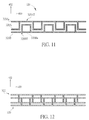
Please see FIG. 10, which shows a schematic diagram of the first layer of the die seal ring according to another embodiment of the present invention. As shown in FIG. 10, the first layer 320 has a first fin ring structure 320A and a second fin ring structure 320B. The first fin ring structure 320A has similar embodiment with that in FIG. 4, and the second fin ring structure 320B is conformal to the first fin ring structure 320A. In this embodiment, a plurality of auxiliary rims can be disposed between each two adjacent turning points. For example, a first auxiliary rim 320Aa is disposed between each two turning points 320AT, and a second auxiliary rim 320Ba is disposed between each two turning points 320BT. Preferably, both the first auxiliary rim 320Aa and the second auxiliary rim 320Bb extend along the first direction 400. In the present embodiment, both the first auxiliary rim 320Aa and the second auxiliary rim 320Bb do not directly contact the turning points 320AT and the turning points 320BT. In another embodiment, as shown in FIG. 11, the first auxiliary rim 320Aa directly contacts the turning points 320AT, and the second auxiliary rim 320Ba directly contacts the turning points 320BT.
Please see FIG. 12, which shows a schematic diagram of the first layer and the second layer according to another embodiment of the present invention. As shown in FIG. 12 in conjunction with FIG. 3, the second layer 322 is disposed above the first layer 320. The layout of the first layer 320 can be any embodiments mentioned above. The layout of the second layer 322 can be the same or different form that of the first layer 320. For example, the second layer 322 can have one or a plurality of lines which are extending along the first direction 400. Preferably, there should be overlapping points or regions between the layout of the first layer 320 and the layout of the second layer 322.
Preferably, the first layer 320 of the die seal ring 308 is formed simultaneously with the fin structure 315 of Fin-FET 314 in the active region 306. More specifically, the first layer 320 and the fin structure 315 are formed by using a “sidewall image transfer (SIT)” process. Please see FIG. 13 to FIG. 17, which show schematic diagrams of method of forming the die seal ring according to one embodiment of the present invention. As shown in FIG. 13, a substrate 301 is provided, such as a silicon substrate, an epitaxial silicon substrate, a silicon germanium substrate, a silicon carbide substrate or a silicon-on-insulator (SOI) substrate. A mask layer 324 is then formed on the substrate 301. In one embodiment, the mask layer 324 can be of a single layer or a multi-layer that can be used as a hard mask. For example, the mask layer 324 can include silicon nitride (SiN), silicon oxynitride (SiON), metal or an advanced pattern film (APF) provided by Applied Material. In another embodiment, the mask layer 324 can include a SiO2/SiN/SiO2 tri-layered structure. Next, a sacrificial layer 326 with a pattern is formed on the mask layer 324. For example, a poly-silicon or an amorphous silicon layer is formed comprehensively on the mask layer 324. A photolithography etching process (PEP) is then carried out to form the sacrificial layer 326 having patterns.
As shown in FIG. 14, a material layer 328, such as a silicon nitride (SiN) layer, is formed conformally on the sacrificial layer 326. The method of forming the material layer 328 can include a chemical vapor deposition (CVD) process or an atomic layer deposition (ALD) process. As shown in FIG. 15, the material layer 328 is anisotropically removed until a top surface of the sacrificial layer 326 and the mask layer 324 is exposed. The material layer 328 becomes a spacer 330 on the sidewall of the sacrificial layer 326. Next, as shown in FIG. 16, the sacrificial layer 326 is completely removed, but the spacers 330 still remain on the mask layer 324.
As shown in FIG. 17, an etching process is performed by using the spacer 330 as a mask to pattern the mask layer 324, thereby forming a patterned mask layer 325. In the subsequent step, another etching process is performed by using the patterned mask layer 325 as a mask to pattern the substrate 301, thereby simultaneously forming the fin structures 315 of Fin-FET 314 in the active region 306 and the first layer 320 of the die seal ring 308 that encompasses the active region 306. In the present invention, the layout of the first layer 320 can have any embodiments or their combinations mentioned above. In another embodiment, the mask layer 324 can be omitted. Accordingly, the fin structures 315 and the first layer 320 can be formed directly by etching the substrate 301 by using the spacer 330 as a mask.
Next, a plurality of Fin-FET forming methods can be further carried out to complete the Fin-FET in the active region 306. In one embodiment, the first layer 320 of the die seal ring 308 can be also subjected to the implant process for forming the source/drain region of the Fin-FET 314, thereby making the first layer 320 conductive. Next, a metal interconnection forming method can be carried out to simultaneously forming the second layer 320 and the metal interconnection system 318. By making the first layer 320 conductive and electrically connect to the second layer, the die seal ring 308 in one embodiment can have the EMI reducing ability.
According to the forming method, it is understood that the material of the first layer 320 is the same as that of the fin structure 315, for example, both of them are formed of semiconductor material such as silicon or germanium. In addition, when the first layer 320 is formed by the SIT process and, the layout of the first layer 320 may have a “double ring” structure, as shown in FIG. 8, which shows the first fin ring structure 320A and the second fin ring structure 320B can be formed by the SIT process so they are conformal to each other. By using the SIT process, the first layer 320 may have multi-numbers of fin ring structures, each of which is conformal to each other. However, it is noted that the first layer 320 can be formed by other manufacturing methods and is not limited thereto.
In summary, the present invention provides a die seal ring and a method of forming the same. The die seal ring includes a first ring structure in which the layout of thereof has a stamp like structure. In this way, the long and thin die seal ring can be more rigid and give a strong protection against stress caused crack, break or peeling during process.
Those skilled in the art will readily observe that numerous modifications and alterations of the device and method may be made while retaining the teachings of the invention. Accordingly, the above disclosure should be construed as limited only by the metes and bounds of the appended claims.

Claims (19)

What is claimed is:
1. A die seal ring, comprising:
a substrate; and
a first layer in contact with and extruding from an uppermost surface of the substrate, wherein the first layer has a first fin ring structure and a layout of the first fin ring structure has a stamp-like shape, wherein the first layer comprises a same semiconductor material as the substrate.
2. The die seal ring according to claim 1, wherein the first layer has a multi-number of fin ring structures, and a layout of each of the fin ring structures has a stamp-like shape.
3. The die seal ring according to claim 1, wherein the first fin ring structure comprises at least a saw-tooth fin rim.
4. The die seal ring according to claim 1, wherein the first fin ring structure comprises at least a serpent fin rim.
5. The die seal ring according to claim 1, wherein the first fin ring structure has at least a zigzag fin rim.
6. The die seal ring according to claim 1, wherein the first layer further comprises a second fin ring structure, wherein a layout of the second fin ring structure is substantially conformal to that of the first fin ring structure.
7. The die seal ring according to claim 6, wherein the first fin ring structure comprises a plurality of first turning points, and the second fin ring structure has a plurality of second turning points, wherein each first turning point corresponds to each second turning point.
8. The die seal ring according to claim 7, wherein the first fin ring structure comprises a first auxiliary rim disposed between each two adjacent first turning points, and the second fin ring structure comprises a second auxiliary rim disposed between each two adjacent second turning points.
9. The die seal ring according to claim 8, wherein each first auxiliary rim directly contacts each two adjacent first turning points, and each second auxiliary rim directly contacts each two adjacent second turning points.
10. The die seal ring according to claim 8, wherein each first auxiliary rim does not contact each two adjacent first turning points, and each second auxiliary rim does not contact each two adjacent second turning points.
11. The die seal ring according to claim 6, wherein the first layer further comprises:
a third fin ring structure; and
a fourth fin ring structure, wherein a layout of the third fin ring structure is substantially conformal to that of the fourth fin ring structure, and the first fin ring structure, the second fin ring structure are symmetric with the third fin ring structure and the fourth fin ring structure.
12. The die seal ring according to claim 1, wherein the die seal ring further comprises a second layer disposed above the first layer, wherein a layout of the second layer overlaps the layout of the first ring structure.
13. The die seal ring according to claim 12, wherein the second layer comprises a metal.
14. The die seal ring according to claim 1, wherein the die seal ring is disposed in a chip, and the chip comprises a plurality of active components that are disposed on the substrate and completely encompassed by the die seal ring.
15. A method for forming a die seal ring, comprising:
providing a substrate having an active region;
forming a patterned sacrificial layer on the substrate;
forming a spacer on sidewalls of the patterned sacrificial layer;
removing the patterned sacrificial layer;
using the spacer as a mask to pattern the substrate, thereby simultaneously forming at least a fin structure of a Fin-FET and a first layer of the die seal ring, wherein the first layer has a fin ring structure.
16. The method for forming a die seal ring according to claim 15, wherein the first layer comprises a semiconductor material.
17. The method for forming a die seal ring according to claim 15, wherein the first layer has a multi-number of fin ring structures, and a layout of each of the fin ring structures has a stamp-like shape.
18. The method for forming a die seal ring according to claim 15, further comprising: simultaneously forming a metal interconnection system in the active region and a second layer of die seal ring.
19. The method for forming a die seal ring according to claim 18, wherein the second layer comprises a metal.
US13/921,174 2013-06-18 2013-06-18 Die seal ring and method of forming the same Active 2033-10-17 US9048246B2 (en)

Priority Applications (1)

Application Number Priority Date Filing Date Title
US13/921,174 US9048246B2 (en) 2013-06-18 2013-06-18 Die seal ring and method of forming the same

Applications Claiming Priority (1)

Application Number Priority Date Filing Date Title
US13/921,174 US9048246B2 (en) 2013-06-18 2013-06-18 Die seal ring and method of forming the same

Publications (2)

Publication Number Publication Date
US20140367835A1 US20140367835A1 (en) 2014-12-18
US9048246B2 true US9048246B2 (en) 2015-06-02

Family

ID=52018530

Family Applications (1)

Application Number Title Priority Date Filing Date
US13/921,174 Active 2033-10-17 US9048246B2 (en) 2013-06-18 2013-06-18 Die seal ring and method of forming the same

Country Status (1)

Country Link
US (1) US9048246B2 (en)

Cited By (1)

* Cited by examiner, † Cited by third party
Publication number Priority date Publication date Assignee Title
US9679896B2 (en) * 2014-12-16 2017-06-13 Samsung Electronics Co., Ltd. Moisture blocking structure and/or a guard ring, a semiconductor device including the same, and a method of manufacturing the same

Families Citing this family (7)

* Cited by examiner, † Cited by third party
Publication number Priority date Publication date Assignee Title
US10163779B2 (en) * 2014-06-12 2018-12-25 Taiwan Semiconductor Manufacturing Company, Ltd. Integrated circuit with guard ring
US9406605B2 (en) * 2014-06-12 2016-08-02 Taiwan Semiconductor Manufacturing Company, Ltd. Integrated circuit with guard ring
US10546822B2 (en) * 2017-08-30 2020-01-28 Globalfoundries Inc. Seal ring structure of integrated circuit and method of forming same
KR20220016332A (en) 2020-07-30 2022-02-09 삼성전자주식회사 Semiconductor device
US11740418B2 (en) 2021-03-23 2023-08-29 Globalfoundries U.S. Inc. Barrier structure with passage for waveguide in photonic integrated circuit
US20220352154A1 (en) * 2021-04-30 2022-11-03 Taiwan Semiconductor Manufacturing Company, Ltd. Integrated circuit having three-dimensional transistors and seal ring structure with monitoring pattern
US20230010037A1 (en) * 2021-07-09 2023-01-12 Taiwan Semiconductor Manufacturing Company, Ltd. Mandrel fin design for double seal ring

Citations (36)

* Cited by examiner, † Cited by third party
Publication number Priority date Publication date Assignee Title
US6043138A (en) 1996-09-16 2000-03-28 Advanced Micro Devices, Inc. Multi-step polysilicon deposition process for boron penetration inhibition
US6492216B1 (en) 2002-02-07 2002-12-10 Taiwan Semiconductor Manufacturing Company Method of forming a transistor with a strained channel
US20040195624A1 (en) 2003-04-04 2004-10-07 National Taiwan University Strained silicon fin field effect transistor
US20050051825A1 (en) 2003-09-09 2005-03-10 Makoto Fujiwara Semiconductor device and manufacturing method thereof
US6921963B2 (en) 2003-01-23 2005-07-26 Advanced Micro Devices, Inc Narrow fin FinFET
US20060099830A1 (en) 2004-11-05 2006-05-11 Varian Semiconductor Equipment Associates, Inc. Plasma implantation using halogenated dopant species to limit deposition of surface layers
US7087477B2 (en) 2001-12-04 2006-08-08 International Business Machines Corporation FinFET SRAM cell using low mobility plane for cell stability and method for forming
US7091551B1 (en) 2005-04-13 2006-08-15 International Business Machines Corporation Four-bit FinFET NVRAM memory device
US20060286729A1 (en) 2005-06-21 2006-12-21 Jack Kavalieros Complementary metal oxide semiconductor integrated circuit using raised source drain and replacement metal gate
US20070105370A1 (en) * 2005-11-08 2007-05-10 Kinderknecht Daniel J Methods for anchoring a seal ring to a substrate using vias and assemblies including an anchored seal ring
US20070108528A1 (en) 2005-11-15 2007-05-17 International Business Machines Corporation Sram cell
US20070158756A1 (en) 2006-01-12 2007-07-12 Lars Dreeskornfeld Production method for a FinFET transistor arrangement, and corresponding FinFET transistor arrangement
US7247887B2 (en) 2005-07-01 2007-07-24 Synopsys, Inc. Segmented channel MOS transistor
US7250658B2 (en) 2003-06-26 2007-07-31 International Business Machines Corporation Hybrid planar and FinFET CMOS devices
US7309626B2 (en) 2005-11-15 2007-12-18 International Business Machines Corporation Quasi self-aligned source/drain FinFET process
US7352034B2 (en) 2005-08-25 2008-04-01 International Business Machines Corporation Semiconductor structures integrating damascene-body FinFET's and planar devices on a common substrate and methods for forming such semiconductor structures
US20080157208A1 (en) 2006-12-29 2008-07-03 Fischer Kevin J Stressed barrier plug slot contact structure for transistor performance enhancement
US7470570B2 (en) 2006-11-14 2008-12-30 International Business Machines Corporation Process for fabrication of FinFETs
US7531437B2 (en) 2004-09-30 2009-05-12 Intel Corporation Method of forming metal gate electrodes using sacrificial gate electrode material and sacrificial gate dielectric material
US20090124097A1 (en) 2007-11-09 2009-05-14 International Business Machines Corporation Method of forming narrow fins in finfet devices with reduced spacing therebetween
US7569857B2 (en) 2006-09-29 2009-08-04 Intel Corporation Dual crystal orientation circuit devices on the same substrate
US20090242964A1 (en) 2006-04-26 2009-10-01 Nxp B.V. Non-volatile memory device
US20090269916A1 (en) 2008-04-28 2009-10-29 Inkuk Kang Methods for fabricating memory cells having fin structures with semicircular top surfaces and rounded top corners and edges
US20100025824A1 (en) * 2008-07-29 2010-02-04 Taiwan Semiconductor Manufacturing Company, Ltd. Structure for Reducing Integrated Circuit Corner Peeling
US20100048027A1 (en) 2008-08-21 2010-02-25 International Business Machines Corporation Smooth and vertical semiconductor fin structure
US20100072553A1 (en) 2008-09-23 2010-03-25 Taiwan Semiconductor Manufacturing Co., Ltd. METAL GATE STRESS FILM FOR MOBILITY ENHANCEMENT IN FinFET DEVICE
US20100144121A1 (en) 2008-12-05 2010-06-10 Cheng-Hung Chang Germanium FinFETs Having Dielectric Punch-Through Stoppers
US20100167506A1 (en) 2008-12-31 2010-07-01 Taiwan Semiconductor Manufacturing Co., Ltd. Inductive plasma doping
US20100207237A1 (en) * 2009-02-17 2010-08-19 Chartered Semiconductor Manufacturing, Ltd. Crack stop structure enhancement of the integrated circuit seal ring
US20120175728A1 (en) * 2011-01-11 2012-07-12 Taiwan Semiconductor Manufacturing Company, Ltd. Seal ring structure for integrated circuit chips
US20120223445A1 (en) * 2011-03-01 2012-09-06 Globalfoundries Inc. Semiconductor device comprising a die seal having an integrated alignment mark
US20140084445A1 (en) * 2012-09-21 2014-03-27 Taiwan Semiconductor Manufacturing Company, Ltd. Thermal Dissipation Through Seal Rings in 3DIC Structure
US20140084444A1 (en) * 2012-09-21 2014-03-27 Taiwan Semiconductor Manufacturing Company, Ltd. Thermal Dissipation Through Seal Rings in 3DIC Structure
US20140124889A1 (en) * 2012-11-05 2014-05-08 Omnivision Technologies, Inc. Die seal ring for integrated circuit system with stacked device wafers
US20140131850A1 (en) * 2012-11-09 2014-05-15 Analog Devices, Inc. Microchip with blocking apparatus and method of fabricating microchip
US20140220735A1 (en) * 2013-02-05 2014-08-07 Taiwan Semiconductor Manufacturing Company, Ltd. Method and Apparatus for a Wafer Seal Ring

Patent Citations (36)

* Cited by examiner, † Cited by third party
Publication number Priority date Publication date Assignee Title
US6043138A (en) 1996-09-16 2000-03-28 Advanced Micro Devices, Inc. Multi-step polysilicon deposition process for boron penetration inhibition
US7087477B2 (en) 2001-12-04 2006-08-08 International Business Machines Corporation FinFET SRAM cell using low mobility plane for cell stability and method for forming
US6492216B1 (en) 2002-02-07 2002-12-10 Taiwan Semiconductor Manufacturing Company Method of forming a transistor with a strained channel
US6921963B2 (en) 2003-01-23 2005-07-26 Advanced Micro Devices, Inc Narrow fin FinFET
US20040195624A1 (en) 2003-04-04 2004-10-07 National Taiwan University Strained silicon fin field effect transistor
US7250658B2 (en) 2003-06-26 2007-07-31 International Business Machines Corporation Hybrid planar and FinFET CMOS devices
US20050051825A1 (en) 2003-09-09 2005-03-10 Makoto Fujiwara Semiconductor device and manufacturing method thereof
US7531437B2 (en) 2004-09-30 2009-05-12 Intel Corporation Method of forming metal gate electrodes using sacrificial gate electrode material and sacrificial gate dielectric material
US20060099830A1 (en) 2004-11-05 2006-05-11 Varian Semiconductor Equipment Associates, Inc. Plasma implantation using halogenated dopant species to limit deposition of surface layers
US7091551B1 (en) 2005-04-13 2006-08-15 International Business Machines Corporation Four-bit FinFET NVRAM memory device
US20060286729A1 (en) 2005-06-21 2006-12-21 Jack Kavalieros Complementary metal oxide semiconductor integrated circuit using raised source drain and replacement metal gate
US7247887B2 (en) 2005-07-01 2007-07-24 Synopsys, Inc. Segmented channel MOS transistor
US7352034B2 (en) 2005-08-25 2008-04-01 International Business Machines Corporation Semiconductor structures integrating damascene-body FinFET's and planar devices on a common substrate and methods for forming such semiconductor structures
US20070105370A1 (en) * 2005-11-08 2007-05-10 Kinderknecht Daniel J Methods for anchoring a seal ring to a substrate using vias and assemblies including an anchored seal ring
US7309626B2 (en) 2005-11-15 2007-12-18 International Business Machines Corporation Quasi self-aligned source/drain FinFET process
US20070108528A1 (en) 2005-11-15 2007-05-17 International Business Machines Corporation Sram cell
US20070158756A1 (en) 2006-01-12 2007-07-12 Lars Dreeskornfeld Production method for a FinFET transistor arrangement, and corresponding FinFET transistor arrangement
US20090242964A1 (en) 2006-04-26 2009-10-01 Nxp B.V. Non-volatile memory device
US7569857B2 (en) 2006-09-29 2009-08-04 Intel Corporation Dual crystal orientation circuit devices on the same substrate
US7470570B2 (en) 2006-11-14 2008-12-30 International Business Machines Corporation Process for fabrication of FinFETs
US20080157208A1 (en) 2006-12-29 2008-07-03 Fischer Kevin J Stressed barrier plug slot contact structure for transistor performance enhancement
US20090124097A1 (en) 2007-11-09 2009-05-14 International Business Machines Corporation Method of forming narrow fins in finfet devices with reduced spacing therebetween
US20090269916A1 (en) 2008-04-28 2009-10-29 Inkuk Kang Methods for fabricating memory cells having fin structures with semicircular top surfaces and rounded top corners and edges
US20100025824A1 (en) * 2008-07-29 2010-02-04 Taiwan Semiconductor Manufacturing Company, Ltd. Structure for Reducing Integrated Circuit Corner Peeling
US20100048027A1 (en) 2008-08-21 2010-02-25 International Business Machines Corporation Smooth and vertical semiconductor fin structure
US20100072553A1 (en) 2008-09-23 2010-03-25 Taiwan Semiconductor Manufacturing Co., Ltd. METAL GATE STRESS FILM FOR MOBILITY ENHANCEMENT IN FinFET DEVICE
US20100144121A1 (en) 2008-12-05 2010-06-10 Cheng-Hung Chang Germanium FinFETs Having Dielectric Punch-Through Stoppers
US20100167506A1 (en) 2008-12-31 2010-07-01 Taiwan Semiconductor Manufacturing Co., Ltd. Inductive plasma doping
US20100207237A1 (en) * 2009-02-17 2010-08-19 Chartered Semiconductor Manufacturing, Ltd. Crack stop structure enhancement of the integrated circuit seal ring
US20120175728A1 (en) * 2011-01-11 2012-07-12 Taiwan Semiconductor Manufacturing Company, Ltd. Seal ring structure for integrated circuit chips
US20120223445A1 (en) * 2011-03-01 2012-09-06 Globalfoundries Inc. Semiconductor device comprising a die seal having an integrated alignment mark
US20140084445A1 (en) * 2012-09-21 2014-03-27 Taiwan Semiconductor Manufacturing Company, Ltd. Thermal Dissipation Through Seal Rings in 3DIC Structure
US20140084444A1 (en) * 2012-09-21 2014-03-27 Taiwan Semiconductor Manufacturing Company, Ltd. Thermal Dissipation Through Seal Rings in 3DIC Structure
US20140124889A1 (en) * 2012-11-05 2014-05-08 Omnivision Technologies, Inc. Die seal ring for integrated circuit system with stacked device wafers
US20140131850A1 (en) * 2012-11-09 2014-05-15 Analog Devices, Inc. Microchip with blocking apparatus and method of fabricating microchip
US20140220735A1 (en) * 2013-02-05 2014-08-07 Taiwan Semiconductor Manufacturing Company, Ltd. Method and Apparatus for a Wafer Seal Ring

Cited By (1)

* Cited by examiner, † Cited by third party
Publication number Priority date Publication date Assignee Title
US9679896B2 (en) * 2014-12-16 2017-06-13 Samsung Electronics Co., Ltd. Moisture blocking structure and/or a guard ring, a semiconductor device including the same, and a method of manufacturing the same

Also Published As

Publication number Publication date
US20140367835A1 (en) 2014-12-18

Similar Documents

Publication Publication Date Title
US9048246B2 (en) Die seal ring and method of forming the same
US11929289B2 (en) Semiconductor device having work-function metal and method of forming the same
KR101496519B1 (en) Dummy FinFET Structure and Method of Making Same
US9455176B2 (en) Manufacturing method for forming semiconductor structure with sub-fin structures
US10319679B2 (en) Semiconductor device
KR101645820B1 (en) Finfet seal ring
US10818556B2 (en) Method for forming a semiconductor structure
US9384978B1 (en) Method of forming trenches
US9087884B1 (en) Manufacturing method of semiconductor device and semiconductor device
US10262903B2 (en) Boundary spacer structure and integration
US10115679B1 (en) Trench structure and method
US10290503B2 (en) Spacer enabled poly gate
US10043675B2 (en) Semiconductor device and method for fabricating the same
CN107579066B (en) Semiconductor device and method for manufacturing the same
TWI689980B (en) Method of wafer dicing and die
CN110246804B (en) Contact structure
US11068635B2 (en) Method of designing a mask and method of manufacturing a semiconductor device using the same
WO2015193939A1 (en) Semiconductor-device manufacturing method and semiconductor device
CN107403754B (en) Semiconductor device, manufacturing method thereof and electronic device
CN110911283A (en) Method for manufacturing transistor of silicon on insulator
US10522613B2 (en) Manufacturing method of a resistance device having a fin
CN108206140B (en) Semiconductor device, manufacturing method thereof and electronic device
US8664114B2 (en) Image sensor and method for fabricating the same
US20160079340A1 (en) Semiconductor device and method for manufacturing the same
CN111480224A (en) Semiconductor product and manufacturing process

Legal Events

Date Code Title Description
AS Assignment

Owner name: UNITED MICROELECTRONICS CORP., TAIWAN

Free format text: ASSIGNMENT OF ASSIGNORS INTEREST;ASSIGNORS:WEI, MING-TE;TSAO, PO-CHAO;YANG, CHING-LI;AND OTHERS;REEL/FRAME:030638/0814

Effective date: 20130610

STCF Information on status: patent grant

Free format text: PATENTED CASE

MAFP Maintenance fee payment

Free format text: PAYMENT OF MAINTENANCE FEE, 4TH YEAR, LARGE ENTITY (ORIGINAL EVENT CODE: M1551); ENTITY STATUS OF PATENT OWNER: LARGE ENTITY

Year of fee payment: 4

AS Assignment

Owner name: MARLIN SEMICONDUCTOR LIMITED, IRELAND

Free format text: ASSIGNMENT OF ASSIGNORS INTEREST;ASSIGNOR:UNITED MICROELECTRONICS CORPORATION;REEL/FRAME:056991/0292

Effective date: 20210618

MAFP Maintenance fee payment

Free format text: PAYMENT OF MAINTENANCE FEE, 8TH YEAR, LARGE ENTITY (ORIGINAL EVENT CODE: M1552); ENTITY STATUS OF PATENT OWNER: LARGE ENTITY

Year of fee payment: 8