US9012299B2 - Metal-insualtor-metal (MIM) device and method of formation thereof - Google Patents
Metal-insualtor-metal (MIM) device and method of formation thereof Download PDFInfo
- Publication number
- US9012299B2 US9012299B2 US14/460,205 US201414460205A US9012299B2 US 9012299 B2 US9012299 B2 US 9012299B2 US 201414460205 A US201414460205 A US 201414460205A US 9012299 B2 US9012299 B2 US 9012299B2
- Authority
- US
- United States
- Prior art keywords
- layer
- electrode
- metal
- oxide
- oxide layer
- Prior art date
- Legal status (The legal status is an assumption and is not a legal conclusion. Google has not performed a legal analysis and makes no representation as to the accuracy of the status listed.)
- Expired - Fee Related
Links
Images


Classifications
-
- H—ELECTRICITY
- H01—ELECTRIC ELEMENTS
- H01G—CAPACITORS; CAPACITORS, RECTIFIERS, DETECTORS, SWITCHING DEVICES OR LIGHT-SENSITIVE DEVICES, OF THE ELECTROLYTIC TYPE
- H01G13/00—Apparatus specially adapted for manufacturing capacitors; Processes specially adapted for manufacturing capacitors not provided for in groups H01G4/00 - H01G11/00
-
- H—ELECTRICITY
- H01—ELECTRIC ELEMENTS
- H01G—CAPACITORS; CAPACITORS, RECTIFIERS, DETECTORS, SWITCHING DEVICES OR LIGHT-SENSITIVE DEVICES, OF THE ELECTROLYTIC TYPE
- H01G4/00—Fixed capacitors; Processes of their manufacture
- H01G4/002—Details
- H01G4/018—Dielectrics
- H01G4/06—Solid dielectrics
- H01G4/08—Inorganic dielectrics
- H01G4/10—Metal-oxide dielectrics
-
- H—ELECTRICITY
- H01—ELECTRIC ELEMENTS
- H01L—SEMICONDUCTOR DEVICES NOT COVERED BY CLASS H10
- H01L27/00—Devices consisting of a plurality of semiconductor or other solid-state components formed in or on a common substrate
- H01L27/02—Devices consisting of a plurality of semiconductor or other solid-state components formed in or on a common substrate including semiconductor components specially adapted for rectifying, oscillating, amplifying or switching and having at least one potential-jump barrier or surface barrier; including integrated passive circuit elements with at least one potential-jump barrier or surface barrier
- H01L27/04—Devices consisting of a plurality of semiconductor or other solid-state components formed in or on a common substrate including semiconductor components specially adapted for rectifying, oscillating, amplifying or switching and having at least one potential-jump barrier or surface barrier; including integrated passive circuit elements with at least one potential-jump barrier or surface barrier the substrate being a semiconductor body
- H01L27/10—Devices consisting of a plurality of semiconductor or other solid-state components formed in or on a common substrate including semiconductor components specially adapted for rectifying, oscillating, amplifying or switching and having at least one potential-jump barrier or surface barrier; including integrated passive circuit elements with at least one potential-jump barrier or surface barrier the substrate being a semiconductor body including a plurality of individual components in a repetitive configuration
- H01L27/101—Devices consisting of a plurality of semiconductor or other solid-state components formed in or on a common substrate including semiconductor components specially adapted for rectifying, oscillating, amplifying or switching and having at least one potential-jump barrier or surface barrier; including integrated passive circuit elements with at least one potential-jump barrier or surface barrier the substrate being a semiconductor body including a plurality of individual components in a repetitive configuration including resistors or capacitors only
-
- H—ELECTRICITY
- H01—ELECTRIC ELEMENTS
- H01L—SEMICONDUCTOR DEVICES NOT COVERED BY CLASS H10
- H01L28/00—Passive two-terminal components without a potential-jump or surface barrier for integrated circuits; Details thereof; Multistep manufacturing processes therefor
- H01L28/40—Capacitors
-
- H—ELECTRICITY
- H01—ELECTRIC ELEMENTS
- H01L—SEMICONDUCTOR DEVICES NOT COVERED BY CLASS H10
- H01L28/00—Passive two-terminal components without a potential-jump or surface barrier for integrated circuits; Details thereof; Multistep manufacturing processes therefor
- H01L28/40—Capacitors
- H01L28/55—Capacitors with a dielectric comprising a perovskite structure material
- H01L28/57—Capacitors with a dielectric comprising a perovskite structure material comprising a barrier layer to prevent diffusion of hydrogen or oxygen
-
- Y—GENERAL TAGGING OF NEW TECHNOLOGICAL DEVELOPMENTS; GENERAL TAGGING OF CROSS-SECTIONAL TECHNOLOGIES SPANNING OVER SEVERAL SECTIONS OF THE IPC; TECHNICAL SUBJECTS COVERED BY FORMER USPC CROSS-REFERENCE ART COLLECTIONS [XRACs] AND DIGESTS
- Y10—TECHNICAL SUBJECTS COVERED BY FORMER USPC
- Y10T—TECHNICAL SUBJECTS COVERED BY FORMER US CLASSIFICATION
- Y10T29/00—Metal working
- Y10T29/43—Electric condenser making
- Y10T29/435—Solid dielectric type
Definitions
- This invention relates generally to memory devices, and more particularly, to Metal-Insulator-Metal (MIM) devices and methods of fabrication thereof.
- MIM Metal-Insulator-Metal
- FIGS. 1 and 2 illustrate a method of fabricating a Metal-Insulator-Metal (MIM) device using etching techniques. Initially, conductive layer 22 is provided on a substrate 20 . Next, an insulating layer 24 is provided on the conductive layer 22 . Then, another conductive layer 26 is provided on the insulating layer 24 . It will be understood that the conductive layers 22 , 26 and insulating layer 24 may be of a variety of materials. (It is further understood that the term “MIM” is used to describe such a device even though, for example, the top and/or bottom layers 22 , 26 may be nonmetallic).
- MIM Metal-Insulator-Metal
- a photoresist layer 28 is provided over the conductive layer 26 and, using standard photolithographic techniques, the photoresist layer 28 is patterned as shown. Using the patterned photoresist layer 28 as a mask, the exposed material is etched away to remove portions of the conductive layer 22 , insulating layer 24 , and conductive layer 26 , to form the remaining MIM stack 30 on the substrate 20 . The photoresist 28 is then removed, resulting in the MIM device 30 including electrode 22 A, insulating layer 24 A, and electrode 26 A formed on the substrate 20 .
- the device stack must be properly formed to ensure proper operation of the device 30 .
- the etchant provide proper, even etching of the materials of the electrodes 22 , 26 and insulating layer 24 , meanwhile leaving the exposed material of the substrate 20 substantially intact (the “selectivity” of the etchant refers to the ability to properly remove selected material while leaving other material in contact therewith substantially intact). While the MIM device 30 of FIG.
- the present invention is a method of fabricating a metal-insulator-metal (MIM) device comprising providing a first electrode, providing an oxide layer on the first electrode, providing a protective layer on the oxide layer, providing an opening through the protective layer to expose a portion of the oxide layer, oxidizing a portion of the first electrode underlying the exposed portion of the oxide layer, and providing a second electrode in contact with the exposed portion of the oxide layer.
- MIM metal-insulator-metal
- MIM metal-insulator-metal
- FIGS. 1-3 illustrate process steps in the formation of a MIM in accordance with a method of the prior art
- FIGS. 4-10 illustrate process steps in the formation of a first embodiment of MIM device in accordance with the present invention
- FIGS. 11-16 illustrate process steps in the formation of a second embodiment of MIM device in accordance with the present invention.
- FIGS. 17-20 illustrate process steps in the formation of a third embodiment of MIM device in accordance with the present invention.
- FIGS. 21-24 illustrate process steps in the formation of a fourth embodiment of MIM device in accordance with the present invention.
- FIGS. 25-30 illustrate process steps in the formation of a fifth embodiment of MIM device in accordance with the present invention.
- FIGS. 31 and 32 illustrate arrays incorporating the invention
- FIGS. 33-35 illustrate systems incorporating the invention.
- a first particular embodiment of MIM i.e. a Ta—TaN electrode/Ta oxide/Al (0.5% Cu)/TiN electrode memory device MIM will now be described with reference to FIGS. 4-10 .
- a conductive layer 30 a dielectric substrate 32 thereon and an interconnect conductive plug 34 (for example Cu or W) in a via in the substrate 32 contacting the conductive layer 30 .
- sequential processing steps are undertaken in a multi-chamber PVD system such as the Applied Materials Endura system, without vacuum break. Initially, degassing is undertaken at 150° C., and Ar+ ion sputter etch is undertaken to remove native metal oxide from the exposed plug 34 surface.
- ⁇ -Ta is deposited on the substrate 32 and plug 34 , to a thickness of 50-150 angstroms, at 200° C.
- fcc TaN is deposited on the ⁇ -Ta to a thickness of 150-350 angstroms, also at 200° C.
- the material of the bottom electrode is Ta or TaN, or combinations thereof.
- Such electrodes have been constructed using 1) ⁇ -Ta (Ta deposited onto a TaN seed layer), 2) pure fcc TaN, and bilayer fcc TaN over ⁇ -Ta).
- the bilayer Ta—TaN film is patterned by photolithography, and the exposed bilayer Ta—TaN film is etched away in an RIE etcher such as the Lam 9600, using a Cl-containing metal etch chemistry well known to those skilled in the art, to form bottom electrode 36 ( FIG. 4 ).
- Photoresist is removed by a combination of mild O 2 plasma and wet solvent techniques.
- the bottom electrode 36 has provided thereon and is encapsulated in protective dielectric layer 38 using a plasma CVD reactor ( FIG. 5 ).
- a plasma CVD reactor FIG. 5 .
- a 300-600 angstroms thick layer of plasma silicon oxynitride (SiON) is deposited from SiH 4 , N 2 O, & N 2 at 350° C.-400° C.
- Photolithography is carried out on the formed protective dielectric layer 38 to pattern a contact opening 40 of 0.1-0.3 ⁇ m diameter on top of the bottom electrode 36 ( FIG. 6 ). Care is taken to position the opening 40 so that it is landed on and exposes a planar and smooth portion of the bottom electrode 36 .
- the contact opening 40 is etched through the dielectric layer 38 in an RIE etch tool such as the TEL DRM etcher, using CHF 3 , O 2 chemistry.
- the etching of layer 38 is initiated through a photoresist mask in place, then the mask is removed with O 2 plasma, and the dielectric etching is completed. This is done to prevent metal re-sputter defects and to slope the opening sidewalls.
- the device is transferred to an oxidation chamber to oxidize a portion of the electrode, growing Ta 2 O 5 layer 42 on the exposed surface of the electrode 36 defined by opening 40 .
- Oxidation can be accomplished by any number of means, including thermal oxidation by O 2 at elevated temperatures (500° C.-800° C.), and reduced-pressure oxidation in an O-containing plasma at somewhat lower temperatures.
- O 2 plasma established in a Gasonics photoresist asher, where the device is downstream of the glow discharge.
- the machine conditions used are 1) 250° C.-300° C.
- the process grows ⁇ 6-15 nm tantalum oxide layer 42 with a gross stoichiometry of Ta 2 O 5 .
- the film is amorphous, with roughness of ⁇ 10 A rms.
- layer 44 of Ta is deposited by PVD onto the resulting structure, i.e., over the layer 38 and the oxide layer 42 ( FIG. 8 ).
- the thin Ta layer 44 is oxidizable and is then completely reacted to Ta 2 O 5 layer 46 by another oxidation process similar to that described above ( FIG. 9 ).
- the two-step oxidation can produce a resulting layered Ta oxide (including oxide layer 42 and the portion of oxide layer 46 thereon and in contact therewith) of ⁇ 12 nm-20 nm thickness.
- a 50-100 angstrom thick layer of Ta 2 O 5 can be directly deposited by reactive-sputter PVD from a Ta target in an O 2 /Ar ambient.
- a thick Ta oxide was reduced in thickness by Ar+ion sputter etching, which tends to produce a Ta-rich layer on the sputtered surface of the oxide.
- the Ta oxide was partially reduced by the chemical interaction with a reactive metal such as Al during a thermal annealing step.
- a layered oxide structure of Al oxide and Ta oxide was produced, with as Ta-rich layer sandwiched in between.
- Cells were fabricated with a range in final Ta 2 O 5 thickness by combining the above techniques and modifying the duration of the oxidation processes.
- the device is then transferred back into the PVD deposition system described above, and a top electrode 48 of Al (0.5% Cu) followed by TiN is deposited, in contact with the portion of the oxidized layer 46 on the oxide layer 42 ( FIG. 10 ).
- a top electrode 48 of Al (0.5% Cu) followed by TiN is deposited, in contact with the portion of the oxidized layer 46 on the oxide layer 42 ( FIG. 10 ).
- the device sequences through degas, followed by 750-4000 angstrom thick deposition of Al (0.5% Cu) at a temperature of 150° C., plus 750-1000 angstroms of TiN at 150° C.
- Low RF power settings ⁇ 5 kW were used during processing to better control the deposition rate and reduce sputter damage to the metal oxide insulator.
- the electrode 48 is patterned by photolithography to create the M2 conductor/top electrode layer contacting oxide 46 and extending above the protective layer 38 .
- the TiN/Al is RIE etched using Cl-containing chemistry in a tool such as the Lam 9600.
- FIGS. 11-16 illustrate a second embodiment of the invention.
- the bottom electrode 36 is formed on the substrate 32 and plug 34 as previously described with reference to FIG. 4 .
- an oxide layer 50 is grown on the entire exposed surface of the electrode 36 in a downstream O 2 plasma at temperatures ranging from 250° C.-300° C.
- some nitrogen was incorporated into the Ta oxide, segregated mostly at the interface with the TaN.
- the thickness of the grown Ta oxide 50 ranged from ⁇ 60 angstroms- ⁇ 150 angstroms, with a thickness uniformity within 20%.
- the formed oxide 50 is principally amorphous Ta oxide with a stoichiometry approximated by Ta 2 O 5 .
- a protective layer 52 is formed as shown and described with regard to FIG. 5 , and ( FIG. 14 ) an opening 54 is provided therein to expose a portion of the oxide layer 50 , using steps similar to those shown and described with regard to FIG. 6 .
- another oxidation step is undertaken ( FIG. 15 ), using the procedures shown and described with regard to FIG. 7 , to oxidize a portion 56 of the electrode 36 underlying the exposed portion of the oxide layer the.
- the top electrode 58 is then formed ( FIG. 16 ) as previously described with regard to FIG. 10 .
- a silicon nitride (SiN) layer 60 is deposited to a thickness of 500-1000 angstroms. This SiN layer 60 is then subjected to an unmasked, anisotropic RIE etchback of an amount slightly exceeding the deposition thickness. The process results in formation of an annular SiN spacer 62 on the walls of the opening 40 , reducing the size of the opening 40 A to a range of 50-200 nm diameter and reducing the size of the exposed portion of the electrode 36 .
- Metal oxide insulator 64 is grown at the bottom of the opening 40 A now defined by the spacer 62 by oxidation of the exposed metal surface of the bottom electrode 36 , using processes shown and described above.
- the top electrode 66 is formed as previously shown and described, in contact with oxide 64 and spacer 62 .
- the cell area is defined by the area at the bottom of the spacer 62 , typically ⁇ 0.0064 ⁇ m 2 .
- FIGS. 21-24 illustrate a fourth embodiment of the invention.
- process steps as shown and described with regard to FIGS. 11-14 are initially undertaken.
- a silicon nitride (SiN) layer 70 is deposited to a thickness of 500-1000 angstroms.
- This SiN layer 70 is then subjected to an unmasked, anisotropic RIE etchback of an amount slightly exceeding the deposition thickness.
- the process results in an annular SiN spacer 72 narrowing the contact opening 54 A to a range of 50-200 nm diameter.
- an oxidation step is undertaken to oxidize a portion 74 of the electrode 36 underlying the exposed portion of the oxide layer 50 , the size of which is determined by the spacer 72 .
- the top electrode 76 is formed as previously shown and described, in contact with oxide 50 and spacer 72 .
- a process will be described for fabricating a Ta/Ta oxide/Ni damascene MIM cell.
- metal interconnect plug 34 is formed in substrate 32 to contact the MIM structure ( FIG. 25 )
- a bi-layer dielectric layer 80 is deposited.
- a 300-1000 angstrom thick layer of plasma silicon nitride (SiN) is deposited from SiH 4 , NH 3 , and N 2 at 350-400 C in an RF-plasma enhanced deposition tool, such as the AMAT Producer or Novellus Concept 2 Sequel.
- a 300-600 angstrom thick film of plasma silicon oxynitride (SiON) is deposited from SiH 4 , N 2 O & N 2 at 350-400 C.
- Photolithography is carried out on the dielectric films to pattern via opening 82 of 0.18 ⁇ m diameter landing on the plug 34 . Opening is etched through the dielectric layer 80 in an RIE etch tool such as the TEL DRM etcher, using CHF 3 , O 2 chemistry. The etching of dielectric 80 is initiated through a photoresist mask, then the mask is removed with O 2 plasma, and the dielectric etching is completed. This is done to prevent metal re-sputter defects and to slope the contact sidewalls.
- a bottom electrode material consisting of ⁇ -Ta is deposited by PVD.
- the device is degassed at 150 C, Ar+ion sputter etched to remove native metal oxide from the plug surface, then deposited with 800-2000 angstroms of ⁇ -Ta at 200° C.
- the excess metal on the surface is removed is removed by CMP polishing, leaving exposed flat electrode 84 of ⁇ -Ta.
- the CMP is carried out on a precision polisher such as the AMAT Mirra, equipped with optical endpoint detection. Planarization is achieved using a hard urethane pad and a silica-abrasive slurry suitable for Ta polish, such as Hitachi T805-1.
- a precision polisher such as the AMAT Mirra
- Planarization is achieved using a hard urethane pad and a silica-abrasive slurry suitable for Ta polish, such as Hitachi T805-1.
- reasonably good selectivity between the Ta and the underlying dielectric 80 is important, as well as a clearly identified Ta polishing endpoint.
- Oxidation can be accomplished by any number of means, including thermal oxidation by O 2 at elevated temperatures (500° C.-800° C.), and reduced-pressure oxidation in an O-containing plasma at somewhat lower temperatures.
- O 2 plasma established in a Gasonics photoresist asher, where the device is downstream of the glow discharge.
- the machine conditions used are 1) 250° C.-300° C.
- the device After oxidation, the device is transferred back into the PVD deposition system described above, and a top electrode 92 of Ni is deposited.
- the device sequences through degas, followed by 100-500 angstrom thick deposition of Ni at a temperature of 30° C.
- Low RF power settings ⁇ 5 kW were used during processing to better control the deposition rate and reduce sputter damage to the metal oxide insulator.
- the device is patterned by photolithography to create the M2 conductor/top electrode layer 92 .
- the Ni is RIE etched using Cl-containing chemistry in a tool such as the Lam 9600.
- the device was fabricated used ⁇ -Ta as the bottom electrode metal. It is possible to use any conductor material as bottom electrode, as long as the material can be deposited into and fill up the via opening to provide a solid plug after CMP. For example TaN, Co, Ni, Cu, Pt, or conductive metal oxides could be used. Metal filling capacity will depend on deposition technique and via aspect ratio as parameters.
- the thickness of the ⁇ -Ta bottom electrodes ranges from 250 angstroms to 900 angstroms.
- the metal oxide insulating layer is principally amorphous tantalum oxide with a stoichiometry approximated by Ta 2 O 5 .
- the thickness of the grown Ta oxide 90 is 60-150 angstroms in the various cells that were tested. Thickness uniformity is within a range of 20%.
- the top electrode metal in contact with the metal oxide insulator may be either Ni or Co, although any appropriate top electrode metal could be used.
- the top electrode metal was deposited at a temperature of 30° C. Low RF power settings were used during processing to better control the deposition rate and reduce sputter damage to the metal oxide insulator.
- the present approach provides various processes for forming metal-insulator-metal devices.
- the various methods are straightforward and efficient in properly forming such devices.
- the problems set forth with regard to etching of materials to form devices is avoided.
- the present approaches provide for a high degree of scalability of devices.
- FIG. 31 illustrates a high density memory device array 150 which incorporates memory devices M as described above ( FIGS. 10 , 16 , 20 , 24 , 30 ) and diodes 39 .
- the memory device array 150 includes a first plurality 152 of parallel conductors (bit lines) BL 0 , BL 1 , . . . BL n , and a second plurality 154 of parallel conductors (word lines) WL 0 , WL 1 , . . . WL n overlying and spaced from, orthogonal to, and crossing the first plurality of conductors 152 .
- a plurality of memory devices M are included, each in series with a diode 39 , to form a memory device-diode structure 162 which connects a bit line with a word line at the intersection thereof, with the diode in a forward direction from the bit line to the word line.
- Each memory device-diode structure 162 may be manufactured as a stacked structure, so that efficient manufacturing thereof is achieved.
- FIG. 32 illustrates a high density memory device array 250 which incorporates memory devices M as described above and transistors 140 .
- the memory device array 250 includes a first plurality 252 of parallel conductors (bit lines) BL 0 , BL 1 , . . . BL n , and a second plurality 254 of parallel conductors (word lines) WL 0 , WL 1 , . . . WL n overlying and spaced from, orthogonal to, and crossing the first plurality of conductors 252 .
- a plurality of memory devices M are included, each in series with a transistor 140 , to form a memory device-transistor structure 262 which connects a bit line with a word line at the intersection thereof.
- the transistors 140 act as select devices for the associated memory devices M.
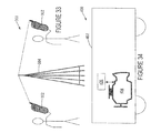
- FIG. 33 illustrates a system 300 utilizing devices as described above.
- the system 300 includes hand-held devices 302 in the form of cell phones, which communicate through an intermediate apparatus such as a tower 304 (shown) and/or a satellite. Signals are provided from one cell phone to the other through the tower 304 .
- a cell phone with advantage uses devices of the type described above.
- One skilled in the art will readily understand the advantage of using such devices in other hand-held devices 302 such as portable media players, personal digital assistants, digital cameras and the like.
- FIG. 34 illustrates another system 400 utilizing devices as described above.
- the system 400 includes a vehicle 402 having an engine 404 controlled by an electronic control unit 406 .
- the electronic control unit 406 with advantage uses devices of the type described.
- FIG. 35 illustrates yet another system 500 utilizing devices as described above.
- This system 500 is a computer 502 which includes an input in the form of a keyboard, and a microprocessor for receiving signals from the keyboard through an interface.
- the microprocessor also communicates with a CDROM drive, a hard drive, and a floppy drive through interfaces. Output from the microprocessor is provided to a monitor through an interface.
- memory Also connected to and communicating with the microprocessor is memory which may take the form of ROM, RAM, flash and/or other forms of memory.
- the system 300 with advantage uses devices of the type described above.
Abstract
Description
Claims (4)
Priority Applications (1)
| Application Number | Priority Date | Filing Date | Title |
|---|---|---|---|
| US14/460,205 US9012299B2 (en) | 2007-10-30 | 2014-08-14 | Metal-insualtor-metal (MIM) device and method of formation thereof |
Applications Claiming Priority (3)
| Application Number | Priority Date | Filing Date | Title |
|---|---|---|---|
| US11/980,213 US8445913B2 (en) | 2007-10-30 | 2007-10-30 | Metal-insulator-metal (MIM) device and method of formation thereof |
| US13/866,898 US8828837B2 (en) | 2007-10-30 | 2013-04-19 | Metal-insulator-metal (MIM) device and method of formation thereof |
| US14/460,205 US9012299B2 (en) | 2007-10-30 | 2014-08-14 | Metal-insualtor-metal (MIM) device and method of formation thereof |
Related Parent Applications (1)
| Application Number | Title | Priority Date | Filing Date |
|---|---|---|---|
| US13/866,898 Division US8828837B2 (en) | 2007-10-30 | 2013-04-19 | Metal-insulator-metal (MIM) device and method of formation thereof |
Publications (2)
| Publication Number | Publication Date |
|---|---|
| US20140357044A1 US20140357044A1 (en) | 2014-12-04 |
| US9012299B2 true US9012299B2 (en) | 2015-04-21 |
Family
ID=40582507
Family Applications (3)
| Application Number | Title | Priority Date | Filing Date |
|---|---|---|---|
| US11/980,213 Active 2028-05-12 US8445913B2 (en) | 2007-10-30 | 2007-10-30 | Metal-insulator-metal (MIM) device and method of formation thereof |
| US13/866,898 Expired - Fee Related US8828837B2 (en) | 2007-10-30 | 2013-04-19 | Metal-insulator-metal (MIM) device and method of formation thereof |
| US14/460,205 Expired - Fee Related US9012299B2 (en) | 2007-10-30 | 2014-08-14 | Metal-insualtor-metal (MIM) device and method of formation thereof |
Family Applications Before (2)
| Application Number | Title | Priority Date | Filing Date |
|---|---|---|---|
| US11/980,213 Active 2028-05-12 US8445913B2 (en) | 2007-10-30 | 2007-10-30 | Metal-insulator-metal (MIM) device and method of formation thereof |
| US13/866,898 Expired - Fee Related US8828837B2 (en) | 2007-10-30 | 2013-04-19 | Metal-insulator-metal (MIM) device and method of formation thereof |
Country Status (1)
| Country | Link |
|---|---|
| US (3) | US8445913B2 (en) |
Families Citing this family (1)
| Publication number | Priority date | Publication date | Assignee | Title |
|---|---|---|---|---|
| US8241944B2 (en) | 2010-07-02 | 2012-08-14 | Micron Technology, Inc. | Resistive RAM devices and methods |
Citations (69)
| Publication number | Priority date | Publication date | Assignee | Title |
|---|---|---|---|---|
| US5708559A (en) | 1995-10-27 | 1998-01-13 | International Business Machines Corporation | Precision analog metal-metal capacitor |
| US5952687A (en) | 1994-09-17 | 1999-09-14 | Kabushiki Kaisha Toshiba | Semiconductor memory device having a trench capacitor with lower electrode inside the trench |
| US5953609A (en) | 1995-12-14 | 1999-09-14 | Nec Corporation | Method of manufacturing a semiconductor memory device |
| US5963818A (en) | 1997-09-17 | 1999-10-05 | Motorola, Inc | Combined trench isolation and inlaid process for integrated circuit formation |
| US6144060A (en) | 1997-07-31 | 2000-11-07 | Samsung Electronics Co., Ltd. | Integrated circuit devices having buffer layers therein which contain metal oxide stabilized by heat treatment under low temperature |
| US6204070B1 (en) | 1997-12-27 | 2001-03-20 | Hyundai Electronics Industries Co., Ltd. | Method for manufacturing ferroelectric capacitor |
| US20010006835A1 (en) | 1999-12-22 | 2001-07-05 | Min-Soo Kim | Method for manufacturing aluminum oxide film for use in a semiconductor device |
| US6337238B1 (en) | 1996-12-11 | 2002-01-08 | Fujitsu Limited | Semiconductor device having a dielectric film and a fabrication process thereof |
| US20020014646A1 (en) | 1997-01-31 | 2002-02-07 | Robert Tsu | Integrated circuit capacitor |
| US6355492B1 (en) | 1997-01-22 | 2002-03-12 | Sony Corporation | Process for the manufacturing of oxide electrodes for ferroelectric capacitor |
| US6388285B1 (en) | 1999-06-04 | 2002-05-14 | International Business Machines Corporation | Feram cell with internal oxygen source and method of oxygen release |
| US20020100924A1 (en) | 2000-03-01 | 2002-08-01 | Rhodes Howard E. | Method of forming dram circuitry |
| US20020127867A1 (en) | 2001-03-12 | 2002-09-12 | Samsung Electronics Co., Ltd. | Semiconductor devices having a hydrogen diffusion barrier layer and methods of fabricating the same |
| US20020192979A1 (en) | 2001-06-13 | 2002-12-19 | Ahn Kie Y. | Dielectric layer forming method and devices formed therewith |
| US6509601B1 (en) | 1998-07-31 | 2003-01-21 | Samsung Electronics Co., Ltd. | Semiconductor memory device having capacitor protection layer and method for manufacturing the same |
| US20030042521A1 (en) | 2000-03-28 | 2003-03-06 | Kabushiki Kaisha Toshiba | Semiconductor device having capacitor and method of manufacturing the same |
| US20030063429A1 (en) | 2001-09-13 | 2003-04-03 | Seiko Epson Corporation | Capacitor, semiconductor device, electro-optic device, method of manufacturing capacitor, method of manufacturing semiconductor device, and electronic apparatus |
| US20030119273A1 (en) * | 2001-12-21 | 2003-06-26 | Sanjeev Aggarwal | Methods of preventing reduction of irox during pzt formation by metalorganic chemical vapor deposition or other processing |
| US20030124794A1 (en) * | 2001-12-31 | 2003-07-03 | Memscap | Electronic component incorporating an integrated circuit and planar microcapacitor |
| US20030183862A1 (en) | 2002-03-26 | 2003-10-02 | Samsung Electronics Co., Ltd. | Semiconductor device having metal-insulator-metal capacitor and fabrication method thereof |
| US20040023416A1 (en) | 2002-08-05 | 2004-02-05 | Gilbert Stephen R. | Method for forming a paraelectric semiconductor device |
| US20040059324A1 (en) | 2001-04-26 | 2004-03-25 | Medtronic, Inc. | Method and system for treatment of atrial tachyarrhythmias |
| US20040056324A1 (en) | 2002-09-23 | 2004-03-25 | Ning Xian J. | MIM capacitor structures and fabrication methods in dual-damascene structures |
| US6734489B2 (en) * | 2001-05-30 | 2004-05-11 | Renesas Technology Corp. | Semiconductor element and MIM-type capacitor formed in different layers of a semiconductor device |
| US20040102014A1 (en) | 2002-11-25 | 2004-05-27 | Ning Xian J. | Method for generating alignment marks for manufacturing mim capacitors |
| US20040113232A1 (en) | 2002-12-13 | 2004-06-17 | Johnson Brian G. | Phase change memory |
| US6821862B2 (en) | 2000-06-27 | 2004-11-23 | Samsung Electronics Co., Ltd. | Methods of manufacturing integrated circuit devices that include a metal oxide layer disposed on another layer to protect the other layer from diffusion of impurities and integrated circuit devices manufactured using same |
| US20050063225A1 (en) | 1996-06-10 | 2005-03-24 | Daisaburo Takashima | Semiconductor memory device and various systems mounting them |
| US20050106761A1 (en) | 2002-06-26 | 2005-05-19 | Moon-Sook Lee | Ferroelectric capacitors with metal oxide for inhibiting fatigue |
| US20050141169A1 (en) | 2003-12-25 | 2005-06-30 | Shinko Electric Industries Co., Ltd. | Capacitor device, electronic parts packaging structure, and method of manufacturing the capacitor device |
| US20050142862A1 (en) | 2003-12-31 | 2005-06-30 | Dongbuanam Semiconductor Inc. | Dual damascene interconnection in semiconductor device and method for forming the same |
| US20050170648A1 (en) | 2001-05-24 | 2005-08-04 | Taiwan Semiconductor Manufacturing Company, Ltd. | Method to solve via poisoning for porous low-k dielectric |
| US20050266633A1 (en) | 2004-05-28 | 2005-12-01 | Jing-Horng Gau | Method for fabricating capacitor |
| US6979847B2 (en) * | 2003-09-22 | 2005-12-27 | Oki Electric Industry Co., Ltd. | Ferroelectric element and method for manufacturing the same |
| US20060022241A1 (en) * | 2004-07-29 | 2006-02-02 | Yoshiro Shimojo | Semiconductor memory device having capacitor using dielectric film, and method of fabricating the same |
| US7041569B1 (en) | 2003-04-09 | 2006-05-09 | Newport Fab, Llc | Method for fabricating a high density composite MIM capacitor with reduced voltage dependence in semiconductor dies |
| US20060145293A1 (en) | 2004-12-30 | 2006-07-06 | Magnachip Semiconductor, Ltd. | Semiconductor device and method for fabricating the same |
| US7075135B2 (en) | 2002-11-21 | 2006-07-11 | Fujitsu Limited | Semiconductor device having a stress layer for applying tensile of compressive stress to the ferroelectric film |
| US7078310B1 (en) | 2003-05-28 | 2006-07-18 | Newport Fab, Llc | Method for fabricating a high density composite MIM capacitor with flexible routing in semiconductor dies |
| US7098497B2 (en) | 2001-12-17 | 2006-08-29 | Kabushiki Kaisha Toshiba | Semiconductor device using high-dielectric-constant material and method of manufacturing the same |
| US7109540B2 (en) | 2003-11-10 | 2006-09-19 | Seiko Epson Corporation | Semiconductor device for restraining short circuiting and method of manufacturing thereof |
| US20060261387A1 (en) | 2003-12-26 | 2006-11-23 | Fujitsu Limited | Semiconductor device and manufacturing method thereof |
| WO2006131968A1 (en) | 2005-06-09 | 2006-12-14 | Fujitsu Limited | Semiconductor device and method for fabricating same |
| US20070007657A1 (en) * | 2004-01-29 | 2007-01-11 | Hineman Max F | Methods for forming conductive vias in a substrate and electronic devices and systems including an at least partially reversed oxidation injury at an interface between a conductive via and a conductive interconnect structure |
| US7180117B2 (en) | 2003-02-05 | 2007-02-20 | Samsung Electronics Co., Ltd. | Flat-type capacitor for integrated circuit and method of manufacturing the same |
| US7208791B2 (en) | 2002-12-11 | 2007-04-24 | Samsung Electronics Co., Ltd. | Integrated circuit devices including a capacitor |
| US7220600B2 (en) | 2004-12-17 | 2007-05-22 | Texas Instruments Incorporated | Ferroelectric capacitor stack etch cleaning methods |
| US7232693B2 (en) | 2004-08-24 | 2007-06-19 | Oki Electric Industry Co., Ltd. | Method for manufacturing ferroelectric memory |
| US20070176243A1 (en) | 2006-01-27 | 2007-08-02 | Fujitsu Limited | Semiconductor device having capacitor capable of reducing additional processes and its manufacture method |
| US7253075B2 (en) | 2002-10-28 | 2007-08-07 | Kabushiki Kaisha Toshiba | Semiconductor device and method for manufacturing the same |
| US7317221B2 (en) | 2003-12-04 | 2008-01-08 | Taiwan Semiconductor Manufacturing Co., Ltd. | High density MIM capacitor structure and fabrication process |
| US20080081380A1 (en) | 2004-12-17 | 2008-04-03 | Texas Instruments Inc. | Method for leakage reduction in fabrication of high-density FRAM arrays |
| US20080142860A1 (en) | 2006-12-13 | 2008-06-19 | Taiwan Semiconductor Manufacturing Co., Ltd. | Method and system for utilizing DRAM components in a system-on-chip |
| US20080151598A1 (en) | 2006-12-26 | 2008-06-26 | Sudhir Kumar Madan | Ferroelectric memory array for implementing a zero cancellation scheme to reduce plateline voltage in ferroelectric memory |
| US20080157071A1 (en) | 2005-10-20 | 2008-07-03 | Samsung Sdi Co., Ltd. | Thin film transistor and flat panel display including the same |
| US20080174017A1 (en) | 2007-01-22 | 2008-07-24 | International Business Machines Corporation | Hybrid interconnect structure for performance improvement and reliability enhancement |
| US20080272357A1 (en) | 2003-03-21 | 2008-11-06 | Samsung Electronics Co., Ltd. | Phase Changeable Memory Device Structures |
| US20090010038A1 (en) | 2006-03-09 | 2009-01-08 | Texas Instruments Incorporated | Low resistance plate line bus architecture |
| US7476584B2 (en) | 2005-06-20 | 2009-01-13 | Samsung Electronics Co., Ltd. | Method of fabricating a semiconductor device with a bit line contact plug |
| US7485915B2 (en) | 2005-06-30 | 2009-02-03 | Kabushiki Kaisha Toshiba | Semiconductor device and method having capacitor and capacitor insulating film that includes preset metal element |
| US7528405B2 (en) | 2002-08-02 | 2009-05-05 | Unity Semiconductor Corporation | Conductive memory stack with sidewall |
| US7557038B2 (en) | 2004-12-23 | 2009-07-07 | Dongbu Electronics Co., Ltd. | Method for fabricating self-aligned contact hole |
| US20090194845A1 (en) * | 2008-01-31 | 2009-08-06 | Thomas Werner | Semiconductor device comprising a capacitor in the metallization system and a method of forming the capacitor |
| US7608510B2 (en) | 2005-04-26 | 2009-10-27 | Ami Semiconductor Belgium Bvba | Alignment of trench for MOS |
| US20090294905A1 (en) | 2005-09-29 | 2009-12-03 | Fujitsu Microelectronics Limited | Semiconductor device |
| US20100019804A1 (en) | 2006-12-27 | 2010-01-28 | Micron Technology, Inc. | Array sense amplifiers, memory devices and systems including same, and methods of operation |
| US7709878B2 (en) | 2007-09-20 | 2010-05-04 | United Microelectronics Corp. | Capacitor structure having butting conductive layer |
| US20110012230A1 (en) * | 2003-04-24 | 2011-01-20 | Fujitsu Semiconductor Limited | Semiconductor device and manufacturing method thereof |
| US20120266174A1 (en) | 2004-03-29 | 2012-10-18 | Sony Computer Entertainment Inc. | Methods and apparatus for achieving thermal management using processing task scheduling |
Family Cites Families (2)
| Publication number | Priority date | Publication date | Assignee | Title |
|---|---|---|---|---|
| US6052271A (en) * | 1994-01-13 | 2000-04-18 | Rohm Co., Ltd. | Ferroelectric capacitor including an iridium oxide layer in the lower electrode |
| FR2839607B1 (en) | 2002-05-07 | 2004-09-10 | Univ Angers | ASSEMBLY OF POWER COMPONENTS ON A PRINTED CIRCUIT AS WELL AS A METHOD FOR OBTAINING SUCH A ASSEMBLY |
-
2007
- 2007-10-30 US US11/980,213 patent/US8445913B2/en active Active
-
2013
- 2013-04-19 US US13/866,898 patent/US8828837B2/en not_active Expired - Fee Related
-
2014
- 2014-08-14 US US14/460,205 patent/US9012299B2/en not_active Expired - Fee Related
Patent Citations (72)
| Publication number | Priority date | Publication date | Assignee | Title |
|---|---|---|---|---|
| US5952687A (en) | 1994-09-17 | 1999-09-14 | Kabushiki Kaisha Toshiba | Semiconductor memory device having a trench capacitor with lower electrode inside the trench |
| US5708559A (en) | 1995-10-27 | 1998-01-13 | International Business Machines Corporation | Precision analog metal-metal capacitor |
| US5953609A (en) | 1995-12-14 | 1999-09-14 | Nec Corporation | Method of manufacturing a semiconductor memory device |
| US20050063225A1 (en) | 1996-06-10 | 2005-03-24 | Daisaburo Takashima | Semiconductor memory device and various systems mounting them |
| US6337238B1 (en) | 1996-12-11 | 2002-01-08 | Fujitsu Limited | Semiconductor device having a dielectric film and a fabrication process thereof |
| US6355492B1 (en) | 1997-01-22 | 2002-03-12 | Sony Corporation | Process for the manufacturing of oxide electrodes for ferroelectric capacitor |
| US20020014646A1 (en) | 1997-01-31 | 2002-02-07 | Robert Tsu | Integrated circuit capacitor |
| US6144060A (en) | 1997-07-31 | 2000-11-07 | Samsung Electronics Co., Ltd. | Integrated circuit devices having buffer layers therein which contain metal oxide stabilized by heat treatment under low temperature |
| US5963818A (en) | 1997-09-17 | 1999-10-05 | Motorola, Inc | Combined trench isolation and inlaid process for integrated circuit formation |
| US6204070B1 (en) | 1997-12-27 | 2001-03-20 | Hyundai Electronics Industries Co., Ltd. | Method for manufacturing ferroelectric capacitor |
| US6509601B1 (en) | 1998-07-31 | 2003-01-21 | Samsung Electronics Co., Ltd. | Semiconductor memory device having capacitor protection layer and method for manufacturing the same |
| US6388285B1 (en) | 1999-06-04 | 2002-05-14 | International Business Machines Corporation | Feram cell with internal oxygen source and method of oxygen release |
| US20010006835A1 (en) | 1999-12-22 | 2001-07-05 | Min-Soo Kim | Method for manufacturing aluminum oxide film for use in a semiconductor device |
| US20020100924A1 (en) | 2000-03-01 | 2002-08-01 | Rhodes Howard E. | Method of forming dram circuitry |
| US20030042521A1 (en) | 2000-03-28 | 2003-03-06 | Kabushiki Kaisha Toshiba | Semiconductor device having capacitor and method of manufacturing the same |
| US6746929B2 (en) | 2000-03-28 | 2004-06-08 | Kabushiki Kaisha Toshiba | Semiconductor device having capacitor and method of manufacturing the same |
| US6821862B2 (en) | 2000-06-27 | 2004-11-23 | Samsung Electronics Co., Ltd. | Methods of manufacturing integrated circuit devices that include a metal oxide layer disposed on another layer to protect the other layer from diffusion of impurities and integrated circuit devices manufactured using same |
| US20050073803A1 (en) | 2000-06-27 | 2005-04-07 | Hag-Ju Cho | Methods of manufacturing integrated circuit devices that include a metal oxide layer disposed on another layer to protect the other layer from diffusion of impurities and integrated circuit devices manufactured using same |
| US20020127867A1 (en) | 2001-03-12 | 2002-09-12 | Samsung Electronics Co., Ltd. | Semiconductor devices having a hydrogen diffusion barrier layer and methods of fabricating the same |
| US20040059324A1 (en) | 2001-04-26 | 2004-03-25 | Medtronic, Inc. | Method and system for treatment of atrial tachyarrhythmias |
| US20050170648A1 (en) | 2001-05-24 | 2005-08-04 | Taiwan Semiconductor Manufacturing Company, Ltd. | Method to solve via poisoning for porous low-k dielectric |
| US6734489B2 (en) * | 2001-05-30 | 2004-05-11 | Renesas Technology Corp. | Semiconductor element and MIM-type capacitor formed in different layers of a semiconductor device |
| US20020192979A1 (en) | 2001-06-13 | 2002-12-19 | Ahn Kie Y. | Dielectric layer forming method and devices formed therewith |
| US20030063429A1 (en) | 2001-09-13 | 2003-04-03 | Seiko Epson Corporation | Capacitor, semiconductor device, electro-optic device, method of manufacturing capacitor, method of manufacturing semiconductor device, and electronic apparatus |
| US7098497B2 (en) | 2001-12-17 | 2006-08-29 | Kabushiki Kaisha Toshiba | Semiconductor device using high-dielectric-constant material and method of manufacturing the same |
| US20030119273A1 (en) * | 2001-12-21 | 2003-06-26 | Sanjeev Aggarwal | Methods of preventing reduction of irox during pzt formation by metalorganic chemical vapor deposition or other processing |
| US20030124794A1 (en) * | 2001-12-31 | 2003-07-03 | Memscap | Electronic component incorporating an integrated circuit and planar microcapacitor |
| US20030183862A1 (en) | 2002-03-26 | 2003-10-02 | Samsung Electronics Co., Ltd. | Semiconductor device having metal-insulator-metal capacitor and fabrication method thereof |
| US20050106761A1 (en) | 2002-06-26 | 2005-05-19 | Moon-Sook Lee | Ferroelectric capacitors with metal oxide for inhibiting fatigue |
| US7528405B2 (en) | 2002-08-02 | 2009-05-05 | Unity Semiconductor Corporation | Conductive memory stack with sidewall |
| US20040023416A1 (en) | 2002-08-05 | 2004-02-05 | Gilbert Stephen R. | Method for forming a paraelectric semiconductor device |
| US20040056324A1 (en) | 2002-09-23 | 2004-03-25 | Ning Xian J. | MIM capacitor structures and fabrication methods in dual-damascene structures |
| US7253075B2 (en) | 2002-10-28 | 2007-08-07 | Kabushiki Kaisha Toshiba | Semiconductor device and method for manufacturing the same |
| US7075135B2 (en) | 2002-11-21 | 2006-07-11 | Fujitsu Limited | Semiconductor device having a stress layer for applying tensile of compressive stress to the ferroelectric film |
| US20040102014A1 (en) | 2002-11-25 | 2004-05-27 | Ning Xian J. | Method for generating alignment marks for manufacturing mim capacitors |
| US7208791B2 (en) | 2002-12-11 | 2007-04-24 | Samsung Electronics Co., Ltd. | Integrated circuit devices including a capacitor |
| US20040113232A1 (en) | 2002-12-13 | 2004-06-17 | Johnson Brian G. | Phase change memory |
| US7180117B2 (en) | 2003-02-05 | 2007-02-20 | Samsung Electronics Co., Ltd. | Flat-type capacitor for integrated circuit and method of manufacturing the same |
| US20080272357A1 (en) | 2003-03-21 | 2008-11-06 | Samsung Electronics Co., Ltd. | Phase Changeable Memory Device Structures |
| US7041569B1 (en) | 2003-04-09 | 2006-05-09 | Newport Fab, Llc | Method for fabricating a high density composite MIM capacitor with reduced voltage dependence in semiconductor dies |
| US20110012230A1 (en) * | 2003-04-24 | 2011-01-20 | Fujitsu Semiconductor Limited | Semiconductor device and manufacturing method thereof |
| US7078310B1 (en) | 2003-05-28 | 2006-07-18 | Newport Fab, Llc | Method for fabricating a high density composite MIM capacitor with flexible routing in semiconductor dies |
| US6979847B2 (en) * | 2003-09-22 | 2005-12-27 | Oki Electric Industry Co., Ltd. | Ferroelectric element and method for manufacturing the same |
| US7109540B2 (en) | 2003-11-10 | 2006-09-19 | Seiko Epson Corporation | Semiconductor device for restraining short circuiting and method of manufacturing thereof |
| US7317221B2 (en) | 2003-12-04 | 2008-01-08 | Taiwan Semiconductor Manufacturing Co., Ltd. | High density MIM capacitor structure and fabrication process |
| US20050141169A1 (en) | 2003-12-25 | 2005-06-30 | Shinko Electric Industries Co., Ltd. | Capacitor device, electronic parts packaging structure, and method of manufacturing the capacitor device |
| US20060261387A1 (en) | 2003-12-26 | 2006-11-23 | Fujitsu Limited | Semiconductor device and manufacturing method thereof |
| US20050142862A1 (en) | 2003-12-31 | 2005-06-30 | Dongbuanam Semiconductor Inc. | Dual damascene interconnection in semiconductor device and method for forming the same |
| US20070007657A1 (en) * | 2004-01-29 | 2007-01-11 | Hineman Max F | Methods for forming conductive vias in a substrate and electronic devices and systems including an at least partially reversed oxidation injury at an interface between a conductive via and a conductive interconnect structure |
| US20120266174A1 (en) | 2004-03-29 | 2012-10-18 | Sony Computer Entertainment Inc. | Methods and apparatus for achieving thermal management using processing task scheduling |
| US20050266633A1 (en) | 2004-05-28 | 2005-12-01 | Jing-Horng Gau | Method for fabricating capacitor |
| US20060022241A1 (en) * | 2004-07-29 | 2006-02-02 | Yoshiro Shimojo | Semiconductor memory device having capacitor using dielectric film, and method of fabricating the same |
| US7232693B2 (en) | 2004-08-24 | 2007-06-19 | Oki Electric Industry Co., Ltd. | Method for manufacturing ferroelectric memory |
| US20080081380A1 (en) | 2004-12-17 | 2008-04-03 | Texas Instruments Inc. | Method for leakage reduction in fabrication of high-density FRAM arrays |
| US7220600B2 (en) | 2004-12-17 | 2007-05-22 | Texas Instruments Incorporated | Ferroelectric capacitor stack etch cleaning methods |
| US7557038B2 (en) | 2004-12-23 | 2009-07-07 | Dongbu Electronics Co., Ltd. | Method for fabricating self-aligned contact hole |
| US20060145293A1 (en) | 2004-12-30 | 2006-07-06 | Magnachip Semiconductor, Ltd. | Semiconductor device and method for fabricating the same |
| US7608510B2 (en) | 2005-04-26 | 2009-10-27 | Ami Semiconductor Belgium Bvba | Alignment of trench for MOS |
| US20100047931A1 (en) | 2005-06-09 | 2010-02-25 | Fujitsu Microelectronics Limited | Semiconductor device and manufacturing method thereof |
| WO2006131968A1 (en) | 2005-06-09 | 2006-12-14 | Fujitsu Limited | Semiconductor device and method for fabricating same |
| US7476584B2 (en) | 2005-06-20 | 2009-01-13 | Samsung Electronics Co., Ltd. | Method of fabricating a semiconductor device with a bit line contact plug |
| US7485915B2 (en) | 2005-06-30 | 2009-02-03 | Kabushiki Kaisha Toshiba | Semiconductor device and method having capacitor and capacitor insulating film that includes preset metal element |
| US20090294905A1 (en) | 2005-09-29 | 2009-12-03 | Fujitsu Microelectronics Limited | Semiconductor device |
| US20080157071A1 (en) | 2005-10-20 | 2008-07-03 | Samsung Sdi Co., Ltd. | Thin film transistor and flat panel display including the same |
| US20070176243A1 (en) | 2006-01-27 | 2007-08-02 | Fujitsu Limited | Semiconductor device having capacitor capable of reducing additional processes and its manufacture method |
| US20090010038A1 (en) | 2006-03-09 | 2009-01-08 | Texas Instruments Incorporated | Low resistance plate line bus architecture |
| US20080142860A1 (en) | 2006-12-13 | 2008-06-19 | Taiwan Semiconductor Manufacturing Co., Ltd. | Method and system for utilizing DRAM components in a system-on-chip |
| US20080151598A1 (en) | 2006-12-26 | 2008-06-26 | Sudhir Kumar Madan | Ferroelectric memory array for implementing a zero cancellation scheme to reduce plateline voltage in ferroelectric memory |
| US20100019804A1 (en) | 2006-12-27 | 2010-01-28 | Micron Technology, Inc. | Array sense amplifiers, memory devices and systems including same, and methods of operation |
| US20080174017A1 (en) | 2007-01-22 | 2008-07-24 | International Business Machines Corporation | Hybrid interconnect structure for performance improvement and reliability enhancement |
| US7709878B2 (en) | 2007-09-20 | 2010-05-04 | United Microelectronics Corp. | Capacitor structure having butting conductive layer |
| US20090194845A1 (en) * | 2008-01-31 | 2009-08-06 | Thomas Werner | Semiconductor device comprising a capacitor in the metallization system and a method of forming the capacitor |
Non-Patent Citations (2)
| Title |
|---|
| Quirk, et al. "Semiconductgor Manufacturing Technology" Prentice Hall, 2001. pp. 309-310. |
| Webster's New World College Dictionary, Fourth Edition pp. 1007, 2008. |
Also Published As
| Publication number | Publication date |
|---|---|
| US20140357044A1 (en) | 2014-12-04 |
| US8445913B2 (en) | 2013-05-21 |
| US8828837B2 (en) | 2014-09-09 |
| US20090109598A1 (en) | 2009-04-30 |
| US20130237030A1 (en) | 2013-09-12 |
Similar Documents
| Publication | Publication Date | Title |
|---|---|---|
| US9431604B2 (en) | Resistive random access memory (RRAM) and method of making | |
| US8951861B2 (en) | Methods of making a high-density nonvolatile memory | |
| JP4785030B2 (en) | Semiconductor device and manufacturing method thereof | |
| WO2010079816A1 (en) | Semiconductor device and manufacturing method therefor | |
| JP3495955B2 (en) | Semiconductor memory device and method of manufacturing the same | |
| JP2001230382A (en) | Contact etching containing no hydrogen for forming ferroelectric capacitor | |
| US7405121B2 (en) | Semiconductor device with capacitors and its manufacture method | |
| JP2003110095A (en) | Integrated circuit and its forming method | |
| US9893276B2 (en) | Switching element, switching element manufacturing method, semiconductor device, and semiconductor device manufacturing method | |
| JP2002076142A (en) | Method for forming charge storage electrode of capacitor | |
| KR20030023143A (en) | Semicinductor devide and fabricating method of the same | |
| KR100291150B1 (en) | Semiconductor memory device and manufacturing method thereof | |
| US6602721B2 (en) | Method for fabricating ferroelectric memory device and method for fabricating the same | |
| US9012299B2 (en) | Metal-insualtor-metal (MIM) device and method of formation thereof | |
| KR20080112689A (en) | Method for forming storage electrode of semiconductor device | |
| US8089113B2 (en) | Damascene metal-insulator-metal (MIM) device | |
| KR20010039520A (en) | Method for manufacturing capacitor of semiconductor memory device using electroplating method | |
| JP2007214353A (en) | Manufacturing method of ferroelectric capacitor and of semiconductor memory | |
| US9305998B2 (en) | Adhesion of ferroelectric material to underlying conductive capacitor plate | |
| WO2005081317A1 (en) | Process for fabricating semiconductor device | |
| JP2003203991A (en) | Manufacturing method for electrode for capacity element | |
| JP2006319355A (en) | Semiconductor device and manufacturing method therefor | |
| JP2004311974A (en) | Manufacturing method of memory, and memory | |
| WO2008004297A1 (en) | Semiconductor device comprising capacitor and method for manufacturing same | |
| JP2006287261A (en) | Semiconductor device and manufacturing method thereof |
Legal Events
| Date | Code | Title | Description |
|---|---|---|---|
| AS | Assignment |
Owner name: SPANSION LLC, CALIFORNIA Free format text: ASSIGNMENT OF ASSIGNORS INTEREST;ASSIGNORS:AVANZINO, STEVEN;FANG, TZU-NING;KAZA, SWAROOP;AND OTHERS;SIGNING DATES FROM 20071012 TO 20071026;REEL/FRAME:034094/0925 |
|
| AS | Assignment |
Owner name: MORGAN STANLEY SENIOR FUNDING, INC., NEW YORK Free format text: SECURITY INTEREST;ASSIGNORS:CYPRESS SEMICONDUCTOR CORPORATION;SPANSION LLC;REEL/FRAME:035240/0429 Effective date: 20150312 |
|
| STCF | Information on status: patent grant |
Free format text: PATENTED CASE |
|
| AS | Assignment |
Owner name: CYPRESS SEMICONDUCTOR CORPORATION, CALIFORNIA Free format text: ASSIGNMENT OF ASSIGNORS INTEREST;ASSIGNOR:SPANSION LLC;REEL/FRAME:035902/0641 Effective date: 20150601 |
|
| AS | Assignment |
Owner name: MONTEREY RESEARCH, LLC, CALIFORNIA Free format text: ASSIGNMENT OF ASSIGNORS INTEREST;ASSIGNOR:CYPRESS SEMICONDUCTOR CORPORATION;REEL/FRAME:044051/0244 Effective date: 20170928 Owner name: SPANSION LLC, CALIFORNIA Free format text: RELEASE BY SECURED PARTY;ASSIGNOR:MORGAN STANLEY SENIOR FUNDING, INC.;REEL/FRAME:044052/0280 Effective date: 20170928 Owner name: CYPRESS SEMICONDUCTOR CORPORATION, CALIFORNIA Free format text: RELEASE BY SECURED PARTY;ASSIGNOR:MORGAN STANLEY SENIOR FUNDING, INC.;REEL/FRAME:044052/0280 Effective date: 20170928 |
|
| AS | Assignment |
Owner name: MONTEREY RESEARCH, LLC, CALIFORNIA Free format text: ASSIGNMENT OF ASSIGNORS INTEREST;ASSIGNOR:CYPRESS SEMICONDUCTOR CORPORATION;REEL/FRAME:044094/0669 Effective date: 20170928 |
|
| MAFP | Maintenance fee payment |
Free format text: PAYMENT OF MAINTENANCE FEE, 4TH YEAR, LARGE ENTITY (ORIGINAL EVENT CODE: M1551); ENTITY STATUS OF PATENT OWNER: LARGE ENTITY Year of fee payment: 4 |
|
| AS | Assignment |
Owner name: MORGAN STANLEY SENIOR FUNDING, INC., NEW YORK Free format text: CORRECTIVE ASSIGNMENT TO CORRECT THE 8647899 PREVIOUSLY RECORDED ON REEL 035240 FRAME 0429. ASSIGNOR(S) HEREBY CONFIRMS THE SECURITY INTERST;ASSIGNORS:CYPRESS SEMICONDUCTOR CORPORATION;SPANSION LLC;REEL/FRAME:058002/0470 Effective date: 20150312 |
|
| FEPP | Fee payment procedure |
Free format text: MAINTENANCE FEE REMINDER MAILED (ORIGINAL EVENT CODE: REM.); ENTITY STATUS OF PATENT OWNER: LARGE ENTITY |
|
| LAPS | Lapse for failure to pay maintenance fees |
Free format text: PATENT EXPIRED FOR FAILURE TO PAY MAINTENANCE FEES (ORIGINAL EVENT CODE: EXP.); ENTITY STATUS OF PATENT OWNER: LARGE ENTITY |
|
| STCH | Information on status: patent discontinuation |
Free format text: PATENT EXPIRED DUE TO NONPAYMENT OF MAINTENANCE FEES UNDER 37 CFR 1.362 |
|
| FP | Lapsed due to failure to pay maintenance fee |
Effective date: 20230421 |