US8900399B2 - Integrated method and system for manufacturing monolithic panels of crystalline solar cells - Google Patents
Integrated method and system for manufacturing monolithic panels of crystalline solar cells Download PDFInfo
- Publication number
- US8900399B2 US8900399B2 US13/050,807 US201113050807A US8900399B2 US 8900399 B2 US8900399 B2 US 8900399B2 US 201113050807 A US201113050807 A US 201113050807A US 8900399 B2 US8900399 B2 US 8900399B2
- Authority
- US
- United States
- Prior art keywords
- multiplicity
- substrates
- support plates
- wafers
- layer
- Prior art date
- Legal status (The legal status is an assumption and is not a legal conclusion. Google has not performed a legal analysis and makes no representation as to the accuracy of the status listed.)
- Expired - Fee Related
Links
- 238000000034 method Methods 0.000 title description 67
- 238000004519 manufacturing process Methods 0.000 title description 53
- 239000000758 substrate Substances 0.000 claims abstract description 62
- 238000005530 etching Methods 0.000 claims abstract description 29
- 238000005229 chemical vapour deposition Methods 0.000 claims abstract description 6
- 235000012431 wafers Nutrition 0.000 claims description 250
- XUIMIQQOPSSXEZ-UHFFFAOYSA-N Silicon Chemical compound [Si] XUIMIQQOPSSXEZ-UHFFFAOYSA-N 0.000 claims description 57
- 229910052710 silicon Inorganic materials 0.000 claims description 56
- 239000010703 silicon Substances 0.000 claims description 56
- 239000000919 ceramic Substances 0.000 claims description 6
- 229910010271 silicon carbide Inorganic materials 0.000 claims description 5
- HBMJWWWQQXIZIP-UHFFFAOYSA-N silicon carbide Chemical compound [Si+]#[C-] HBMJWWWQQXIZIP-UHFFFAOYSA-N 0.000 claims description 3
- 239000010410 layer Substances 0.000 description 220
- 210000004027 cell Anatomy 0.000 description 193
- 239000010408 film Substances 0.000 description 57
- 230000008569 process Effects 0.000 description 51
- 238000000926 separation method Methods 0.000 description 48
- 229910021426 porous silicon Inorganic materials 0.000 description 41
- 206010040844 Skin exfoliation Diseases 0.000 description 39
- 238000012545 processing Methods 0.000 description 25
- 238000002048 anodisation reaction Methods 0.000 description 24
- 239000003292 glue Substances 0.000 description 24
- 239000002243 precursor Substances 0.000 description 21
- 239000011521 glass Substances 0.000 description 20
- 239000000463 material Substances 0.000 description 18
- 229910052751 metal Inorganic materials 0.000 description 17
- 239000002184 metal Substances 0.000 description 17
- 230000015572 biosynthetic process Effects 0.000 description 15
- 230000009471 action Effects 0.000 description 14
- 238000000151 deposition Methods 0.000 description 13
- 229910021421 monocrystalline silicon Inorganic materials 0.000 description 13
- 238000000866 electrolytic etching Methods 0.000 description 12
- 230000008021 deposition Effects 0.000 description 11
- 239000005038 ethylene vinyl acetate Substances 0.000 description 11
- 229920001200 poly(ethylene-vinyl acetate) Polymers 0.000 description 11
- 239000000243 solution Substances 0.000 description 11
- 238000010438 heat treatment Methods 0.000 description 9
- 239000010409 thin film Substances 0.000 description 9
- KRHYYFGTRYWZRS-UHFFFAOYSA-N Fluorane Chemical compound F KRHYYFGTRYWZRS-UHFFFAOYSA-N 0.000 description 8
- 239000007789 gas Substances 0.000 description 8
- 238000009499 grossing Methods 0.000 description 8
- 238000003491 array Methods 0.000 description 7
- 238000005538 encapsulation Methods 0.000 description 7
- 239000004065 semiconductor Substances 0.000 description 7
- 238000004299 exfoliation Methods 0.000 description 6
- 239000000843 powder Substances 0.000 description 6
- BQCADISMDOOEFD-UHFFFAOYSA-N Silver Chemical compound [Ag] BQCADISMDOOEFD-UHFFFAOYSA-N 0.000 description 5
- 230000008901 benefit Effects 0.000 description 5
- 238000005137 deposition process Methods 0.000 description 5
- 238000009792 diffusion process Methods 0.000 description 5
- 230000000750 progressive effect Effects 0.000 description 5
- 229910052709 silver Inorganic materials 0.000 description 5
- 239000004332 silver Substances 0.000 description 5
- 238000013459 approach Methods 0.000 description 4
- 239000013078 crystal Substances 0.000 description 4
- 239000002019 doping agent Substances 0.000 description 4
- 239000008151 electrolyte solution Substances 0.000 description 4
- 238000000227 grinding Methods 0.000 description 4
- 238000005498 polishing Methods 0.000 description 4
- 230000009467 reduction Effects 0.000 description 4
- 239000002344 surface layer Substances 0.000 description 4
- 230000003746 surface roughness Effects 0.000 description 4
- RYGMFSIKBFXOCR-UHFFFAOYSA-N Copper Chemical compound [Cu] RYGMFSIKBFXOCR-UHFFFAOYSA-N 0.000 description 3
- ATJFFYVFTNAWJD-UHFFFAOYSA-N Tin Chemical compound [Sn] ATJFFYVFTNAWJD-UHFFFAOYSA-N 0.000 description 3
- 239000000853 adhesive Substances 0.000 description 3
- 230000001070 adhesive effect Effects 0.000 description 3
- 238000005452 bending Methods 0.000 description 3
- 238000006243 chemical reaction Methods 0.000 description 3
- 239000004020 conductor Substances 0.000 description 3
- 229910052802 copper Inorganic materials 0.000 description 3
- 239000010949 copper Substances 0.000 description 3
- 230000002950 deficient Effects 0.000 description 3
- 229920005570 flexible polymer Polymers 0.000 description 3
- 239000001257 hydrogen Substances 0.000 description 3
- 229910052739 hydrogen Inorganic materials 0.000 description 3
- 238000011065 in-situ storage Methods 0.000 description 3
- 239000007788 liquid Substances 0.000 description 3
- 238000001465 metallisation Methods 0.000 description 3
- 238000007650 screen-printing Methods 0.000 description 3
- UFHFLCQGNIYNRP-UHFFFAOYSA-N Hydrogen Chemical compound [H][H] UFHFLCQGNIYNRP-UHFFFAOYSA-N 0.000 description 2
- VYPSYNLAJGMNEJ-UHFFFAOYSA-N Silicium dioxide Chemical compound O=[Si]=O VYPSYNLAJGMNEJ-UHFFFAOYSA-N 0.000 description 2
- PNEYBMLMFCGWSK-UHFFFAOYSA-N aluminium oxide Inorganic materials [O-2].[O-2].[O-2].[Al+3].[Al+3] PNEYBMLMFCGWSK-UHFFFAOYSA-N 0.000 description 2
- 238000007743 anodising Methods 0.000 description 2
- 239000006117 anti-reflective coating Substances 0.000 description 2
- 239000011195 cermet Substances 0.000 description 2
- 239000002131 composite material Substances 0.000 description 2
- 230000001143 conditioned effect Effects 0.000 description 2
- 230000003750 conditioning effect Effects 0.000 description 2
- 230000035613 defoliation Effects 0.000 description 2
- 238000011161 development Methods 0.000 description 2
- 238000009826 distribution Methods 0.000 description 2
- 239000003792 electrolyte Substances 0.000 description 2
- 238000005516 engineering process Methods 0.000 description 2
- 238000010304 firing Methods 0.000 description 2
- 230000000977 initiatory effect Effects 0.000 description 2
- 239000000203 mixture Substances 0.000 description 2
- QPJSUIGXIBEQAC-UHFFFAOYSA-N n-(2,4-dichloro-5-propan-2-yloxyphenyl)acetamide Chemical compound CC(C)OC1=CC(NC(C)=O)=C(Cl)C=C1Cl QPJSUIGXIBEQAC-UHFFFAOYSA-N 0.000 description 2
- 238000004806 packaging method and process Methods 0.000 description 2
- BASFCYQUMIYNBI-UHFFFAOYSA-N platinum Chemical compound [Pt] BASFCYQUMIYNBI-UHFFFAOYSA-N 0.000 description 2
- 229910021420 polycrystalline silicon Inorganic materials 0.000 description 2
- 229920005591 polysilicon Polymers 0.000 description 2
- 238000005245 sintering Methods 0.000 description 2
- 238000005476 soldering Methods 0.000 description 2
- 238000005728 strengthening Methods 0.000 description 2
- 238000012360 testing method Methods 0.000 description 2
- ZDHXKXAHOVTTAH-UHFFFAOYSA-N trichlorosilane Chemical compound Cl[SiH](Cl)Cl ZDHXKXAHOVTTAH-UHFFFAOYSA-N 0.000 description 2
- 239000005052 trichlorosilane Substances 0.000 description 2
- 238000004148 unit process Methods 0.000 description 2
- RZVAJINKPMORJF-UHFFFAOYSA-N Acetaminophen Chemical compound CC(=O)NC1=CC=C(O)C=C1 RZVAJINKPMORJF-UHFFFAOYSA-N 0.000 description 1
- 229910052580 B4C Inorganic materials 0.000 description 1
- 229910052582 BN Inorganic materials 0.000 description 1
- PZNSFCLAULLKQX-UHFFFAOYSA-N Boron nitride Chemical compound N#B PZNSFCLAULLKQX-UHFFFAOYSA-N 0.000 description 1
- 229910016347 CuSn Inorganic materials 0.000 description 1
- 238000002231 Czochralski process Methods 0.000 description 1
- 239000004593 Epoxy Substances 0.000 description 1
- 229910000502 Li-aluminosilicate Inorganic materials 0.000 description 1
- 229910052581 Si3N4 Inorganic materials 0.000 description 1
- CPFNXHQBAHTVKB-UHFFFAOYSA-N [Ti].[Cu].[W] Chemical compound [Ti].[Cu].[W] CPFNXHQBAHTVKB-UHFFFAOYSA-N 0.000 description 1
- 230000004913 activation Effects 0.000 description 1
- 239000002313 adhesive film Substances 0.000 description 1
- 239000002390 adhesive tape Substances 0.000 description 1
- HZVVJJIYJKGMFL-UHFFFAOYSA-N almasilate Chemical compound O.[Mg+2].[Al+3].[Al+3].O[Si](O)=O.O[Si](O)=O HZVVJJIYJKGMFL-UHFFFAOYSA-N 0.000 description 1
- 239000005354 aluminosilicate glass Substances 0.000 description 1
- 229910021417 amorphous silicon Inorganic materials 0.000 description 1
- 238000000137 annealing Methods 0.000 description 1
- 239000010426 asphalt Substances 0.000 description 1
- QVGXLLKOCUKJST-UHFFFAOYSA-N atomic oxygen Chemical compound [O] QVGXLLKOCUKJST-UHFFFAOYSA-N 0.000 description 1
- INAHAJYZKVIDIZ-UHFFFAOYSA-N boron carbide Chemical compound B12B3B4C32B41 INAHAJYZKVIDIZ-UHFFFAOYSA-N 0.000 description 1
- 239000013590 bulk material Substances 0.000 description 1
- DQXBYHZEEUGOBF-UHFFFAOYSA-N but-3-enoic acid;ethene Chemical compound C=C.OC(=O)CC=C DQXBYHZEEUGOBF-UHFFFAOYSA-N 0.000 description 1
- ZTXONRUJVYXVTJ-UHFFFAOYSA-N chromium copper Chemical compound [Cr][Cu][Cr] ZTXONRUJVYXVTJ-UHFFFAOYSA-N 0.000 description 1
- 210000000078 claw Anatomy 0.000 description 1
- 238000004140 cleaning Methods 0.000 description 1
- PMHQVHHXPFUNSP-UHFFFAOYSA-M copper(1+);methylsulfanylmethane;bromide Chemical compound Br[Cu].CSC PMHQVHHXPFUNSP-UHFFFAOYSA-M 0.000 description 1
- 229910052878 cordierite Inorganic materials 0.000 description 1
- 229910021419 crystalline silicon Inorganic materials 0.000 description 1
- XLJMAIOERFSOGZ-UHFFFAOYSA-M cyanate Chemical compound [O-]C#N XLJMAIOERFSOGZ-UHFFFAOYSA-M 0.000 description 1
- 230000001351 cycling effect Effects 0.000 description 1
- 230000003247 decreasing effect Effects 0.000 description 1
- 230000007547 defect Effects 0.000 description 1
- 230000007812 deficiency Effects 0.000 description 1
- 238000013461 design Methods 0.000 description 1
- JSKIRARMQDRGJZ-UHFFFAOYSA-N dimagnesium dioxido-bis[(1-oxido-3-oxo-2,4,6,8,9-pentaoxa-1,3-disila-5,7-dialuminabicyclo[3.3.1]nonan-7-yl)oxy]silane Chemical compound [Mg++].[Mg++].[O-][Si]([O-])(O[Al]1O[Al]2O[Si](=O)O[Si]([O-])(O1)O2)O[Al]1O[Al]2O[Si](=O)O[Si]([O-])(O1)O2 JSKIRARMQDRGJZ-UHFFFAOYSA-N 0.000 description 1
- KZHJGOXRZJKJNY-UHFFFAOYSA-N dioxosilane;oxo(oxoalumanyloxy)alumane Chemical compound O=[Si]=O.O=[Si]=O.O=[Al]O[Al]=O.O=[Al]O[Al]=O.O=[Al]O[Al]=O KZHJGOXRZJKJNY-UHFFFAOYSA-N 0.000 description 1
- 230000000694 effects Effects 0.000 description 1
- 239000008393 encapsulating agent Substances 0.000 description 1
- 230000007613 environmental effect Effects 0.000 description 1
- 125000003700 epoxy group Chemical group 0.000 description 1
- 239000000835 fiber Substances 0.000 description 1
- 239000000945 filler Substances 0.000 description 1
- 238000005111 flow chemistry technique Methods 0.000 description 1
- 229910021485 fumed silica Inorganic materials 0.000 description 1
- PCHJSUWPFVWCPO-UHFFFAOYSA-N gold Chemical compound [Au] PCHJSUWPFVWCPO-UHFFFAOYSA-N 0.000 description 1
- 229910052737 gold Inorganic materials 0.000 description 1
- 239000010931 gold Substances 0.000 description 1
- 230000005484 gravity Effects 0.000 description 1
- 125000005842 heteroatom Chemical group 0.000 description 1
- 150000002431 hydrogen Chemical class 0.000 description 1
- 238000002513 implantation Methods 0.000 description 1
- 239000004615 ingredient Substances 0.000 description 1
- 239000011810 insulating material Substances 0.000 description 1
- 210000004692 intercellular junction Anatomy 0.000 description 1
- 238000005304 joining Methods 0.000 description 1
- 238000003475 lamination Methods 0.000 description 1
- 238000003698 laser cutting Methods 0.000 description 1
- 239000011244 liquid electrolyte Substances 0.000 description 1
- 238000003754 machining Methods 0.000 description 1
- 230000000873 masking effect Effects 0.000 description 1
- 239000000155 melt Substances 0.000 description 1
- 150000002739 metals Chemical class 0.000 description 1
- 229910052863 mullite Inorganic materials 0.000 description 1
- 230000003287 optical effect Effects 0.000 description 1
- 239000001301 oxygen Substances 0.000 description 1
- 229910052760 oxygen Inorganic materials 0.000 description 1
- 238000012856 packing Methods 0.000 description 1
- 239000002245 particle Substances 0.000 description 1
- 238000002161 passivation Methods 0.000 description 1
- 238000000059 patterning Methods 0.000 description 1
- 238000001020 plasma etching Methods 0.000 description 1
- 229920003023 plastic Polymers 0.000 description 1
- 239000004033 plastic Substances 0.000 description 1
- 229910052697 platinum Inorganic materials 0.000 description 1
- 229920000647 polyepoxide Polymers 0.000 description 1
- 229920000642 polymer Polymers 0.000 description 1
- 229920000307 polymer substrate Polymers 0.000 description 1
- 229920002635 polyurethane Polymers 0.000 description 1
- 239000004814 polyurethane Substances 0.000 description 1
- 229920002620 polyvinyl fluoride Polymers 0.000 description 1
- 238000002360 preparation method Methods 0.000 description 1
- 238000003825 pressing Methods 0.000 description 1
- 238000007639 printing Methods 0.000 description 1
- 239000005297 pyrex Substances 0.000 description 1
- 239000010453 quartz Substances 0.000 description 1
- 230000001105 regulatory effect Effects 0.000 description 1
- 229920005989 resin Polymers 0.000 description 1
- 239000011347 resin Substances 0.000 description 1
- 238000005096 rolling process Methods 0.000 description 1
- 239000000523 sample Substances 0.000 description 1
- 150000003376 silicon Chemical class 0.000 description 1
- HQVNEWCFYHHQES-UHFFFAOYSA-N silicon nitride Chemical compound N12[Si]34N5[Si]62N3[Si]51N64 HQVNEWCFYHHQES-UHFFFAOYSA-N 0.000 description 1
- 239000012686 silicon precursor Substances 0.000 description 1
- 239000002210 silicon-based material Substances 0.000 description 1
- 239000002002 slurry Substances 0.000 description 1
- 238000010561 standard procedure Methods 0.000 description 1
- 238000003860 storage Methods 0.000 description 1
- 238000004381 surface treatment Methods 0.000 description 1
- 238000002230 thermal chemical vapour deposition Methods 0.000 description 1
Images


Classifications
-
- H—ELECTRICITY
- H01—ELECTRIC ELEMENTS
- H01L—SEMICONDUCTOR DEVICES NOT COVERED BY CLASS H10
- H01L31/00—Semiconductor devices sensitive to infrared radiation, light, electromagnetic radiation of shorter wavelength or corpuscular radiation and specially adapted either for the conversion of the energy of such radiation into electrical energy or for the control of electrical energy by such radiation; Processes or apparatus specially adapted for the manufacture or treatment thereof or of parts thereof; Details thereof
- H01L31/18—Processes or apparatus specially adapted for the manufacture or treatment of these devices or of parts thereof
- H01L31/1876—Particular processes or apparatus for batch treatment of the devices
-
- H—ELECTRICITY
- H01—ELECTRIC ELEMENTS
- H01L—SEMICONDUCTOR DEVICES NOT COVERED BY CLASS H10
- H01L21/00—Processes or apparatus adapted for the manufacture or treatment of semiconductor or solid state devices or of parts thereof
- H01L21/67—Apparatus specially adapted for handling semiconductor or electric solid state devices during manufacture or treatment thereof; Apparatus specially adapted for handling wafers during manufacture or treatment of semiconductor or electric solid state devices or components ; Apparatus not specifically provided for elsewhere
- H01L21/683—Apparatus specially adapted for handling semiconductor or electric solid state devices during manufacture or treatment thereof; Apparatus specially adapted for handling wafers during manufacture or treatment of semiconductor or electric solid state devices or components ; Apparatus not specifically provided for elsewhere for supporting or gripping
- H01L21/687—Apparatus specially adapted for handling semiconductor or electric solid state devices during manufacture or treatment thereof; Apparatus specially adapted for handling wafers during manufacture or treatment of semiconductor or electric solid state devices or components ; Apparatus not specifically provided for elsewhere for supporting or gripping using mechanical means, e.g. chucks, clamps or pinches
- H01L21/68714—Apparatus specially adapted for handling semiconductor or electric solid state devices during manufacture or treatment thereof; Apparatus specially adapted for handling wafers during manufacture or treatment of semiconductor or electric solid state devices or components ; Apparatus not specifically provided for elsewhere for supporting or gripping using mechanical means, e.g. chucks, clamps or pinches the wafers being placed on a susceptor, stage or support
- H01L21/68728—Apparatus specially adapted for handling semiconductor or electric solid state devices during manufacture or treatment thereof; Apparatus specially adapted for handling wafers during manufacture or treatment of semiconductor or electric solid state devices or components ; Apparatus not specifically provided for elsewhere for supporting or gripping using mechanical means, e.g. chucks, clamps or pinches the wafers being placed on a susceptor, stage or support characterised by a plurality of separate clamping members, e.g. clamping fingers
-
- H—ELECTRICITY
- H01—ELECTRIC ELEMENTS
- H01L—SEMICONDUCTOR DEVICES NOT COVERED BY CLASS H10
- H01L31/00—Semiconductor devices sensitive to infrared radiation, light, electromagnetic radiation of shorter wavelength or corpuscular radiation and specially adapted either for the conversion of the energy of such radiation into electrical energy or for the control of electrical energy by such radiation; Processes or apparatus specially adapted for the manufacture or treatment thereof or of parts thereof; Details thereof
- H01L31/04—Semiconductor devices sensitive to infrared radiation, light, electromagnetic radiation of shorter wavelength or corpuscular radiation and specially adapted either for the conversion of the energy of such radiation into electrical energy or for the control of electrical energy by such radiation; Processes or apparatus specially adapted for the manufacture or treatment thereof or of parts thereof; Details thereof adapted as photovoltaic [PV] conversion devices
- H01L31/042—PV modules or arrays of single PV cells
- H01L31/048—Encapsulation of modules
-
- H—ELECTRICITY
- H01—ELECTRIC ELEMENTS
- H01L—SEMICONDUCTOR DEVICES NOT COVERED BY CLASS H10
- H01L31/00—Semiconductor devices sensitive to infrared radiation, light, electromagnetic radiation of shorter wavelength or corpuscular radiation and specially adapted either for the conversion of the energy of such radiation into electrical energy or for the control of electrical energy by such radiation; Processes or apparatus specially adapted for the manufacture or treatment thereof or of parts thereof; Details thereof
- H01L31/18—Processes or apparatus specially adapted for the manufacture or treatment of these devices or of parts thereof
- H01L31/1804—Processes or apparatus specially adapted for the manufacture or treatment of these devices or of parts thereof comprising only elements of Group IV of the Periodic System
-
- H—ELECTRICITY
- H01—ELECTRIC ELEMENTS
- H01L—SEMICONDUCTOR DEVICES NOT COVERED BY CLASS H10
- H01L31/00—Semiconductor devices sensitive to infrared radiation, light, electromagnetic radiation of shorter wavelength or corpuscular radiation and specially adapted either for the conversion of the energy of such radiation into electrical energy or for the control of electrical energy by such radiation; Processes or apparatus specially adapted for the manufacture or treatment thereof or of parts thereof; Details thereof
- H01L31/18—Processes or apparatus specially adapted for the manufacture or treatment of these devices or of parts thereof
- H01L31/1892—Processes or apparatus specially adapted for the manufacture or treatment of these devices or of parts thereof methods involving the use of temporary, removable substrates
-
- H—ELECTRICITY
- H01—ELECTRIC ELEMENTS
- H01L—SEMICONDUCTOR DEVICES NOT COVERED BY CLASS H10
- H01L31/00—Semiconductor devices sensitive to infrared radiation, light, electromagnetic radiation of shorter wavelength or corpuscular radiation and specially adapted either for the conversion of the energy of such radiation into electrical energy or for the control of electrical energy by such radiation; Processes or apparatus specially adapted for the manufacture or treatment thereof or of parts thereof; Details thereof
- H01L31/04—Semiconductor devices sensitive to infrared radiation, light, electromagnetic radiation of shorter wavelength or corpuscular radiation and specially adapted either for the conversion of the energy of such radiation into electrical energy or for the control of electrical energy by such radiation; Processes or apparatus specially adapted for the manufacture or treatment thereof or of parts thereof; Details thereof adapted as photovoltaic [PV] conversion devices
- H01L31/06—Semiconductor devices sensitive to infrared radiation, light, electromagnetic radiation of shorter wavelength or corpuscular radiation and specially adapted either for the conversion of the energy of such radiation into electrical energy or for the control of electrical energy by such radiation; Processes or apparatus specially adapted for the manufacture or treatment thereof or of parts thereof; Details thereof adapted as photovoltaic [PV] conversion devices characterised by at least one potential-jump barrier or surface barrier
- H01L31/068—Semiconductor devices sensitive to infrared radiation, light, electromagnetic radiation of shorter wavelength or corpuscular radiation and specially adapted either for the conversion of the energy of such radiation into electrical energy or for the control of electrical energy by such radiation; Processes or apparatus specially adapted for the manufacture or treatment thereof or of parts thereof; Details thereof adapted as photovoltaic [PV] conversion devices characterised by at least one potential-jump barrier or surface barrier the potential barriers being only of the PN homojunction type, e.g. bulk silicon PN homojunction solar cells or thin film polycrystalline silicon PN homojunction solar cells
-
- Y—GENERAL TAGGING OF NEW TECHNOLOGICAL DEVELOPMENTS; GENERAL TAGGING OF CROSS-SECTIONAL TECHNOLOGIES SPANNING OVER SEVERAL SECTIONS OF THE IPC; TECHNICAL SUBJECTS COVERED BY FORMER USPC CROSS-REFERENCE ART COLLECTIONS [XRACs] AND DIGESTS
- Y02—TECHNOLOGIES OR APPLICATIONS FOR MITIGATION OR ADAPTATION AGAINST CLIMATE CHANGE
- Y02E—REDUCTION OF GREENHOUSE GAS [GHG] EMISSIONS, RELATED TO ENERGY GENERATION, TRANSMISSION OR DISTRIBUTION
- Y02E10/00—Energy generation through renewable energy sources
- Y02E10/50—Photovoltaic [PV] energy
- Y02E10/547—Monocrystalline silicon PV cells
-
- Y—GENERAL TAGGING OF NEW TECHNOLOGICAL DEVELOPMENTS; GENERAL TAGGING OF CROSS-SECTIONAL TECHNOLOGIES SPANNING OVER SEVERAL SECTIONS OF THE IPC; TECHNICAL SUBJECTS COVERED BY FORMER USPC CROSS-REFERENCE ART COLLECTIONS [XRACs] AND DIGESTS
- Y02—TECHNOLOGIES OR APPLICATIONS FOR MITIGATION OR ADAPTATION AGAINST CLIMATE CHANGE
- Y02P—CLIMATE CHANGE MITIGATION TECHNOLOGIES IN THE PRODUCTION OR PROCESSING OF GOODS
- Y02P70/00—Climate change mitigation technologies in the production process for final industrial or consumer products
- Y02P70/50—Manufacturing or production processes characterised by the final manufactured product
Definitions
- This invention relates generally to methods and systems for fabricating solar cells. More particularly, it relates to fabricating an array of solar cells by simultaneously processing commonly supported mother wafers, enabling the simultaneous growth of multiple photovoltaic cell structures.
- Silicon is the basic ingredient of many solar cell technologies ranging from thin film amorphous silicon solar cells to single-crystal silicon wafer-based solar cells.
- High efficiency solar cells start with electronic grade polysilicon grown by chemical vapor deposition.
- the polysilicon is melted and ingots are pulled from the melt in the Czochralski process and often zone refined to produce silicon ingots or ribbons of different degrees of crystal perfection.
- the silicon ingot is then sliced into thin wafers by sawing or laser cutting, and solar cells are formed on the wafers by traditional semiconductor techniques and interconnected and packaged to last at least 25 years.
- Such silicon wafers are relatively expensive and thus severely impact the costs of solar cells in formed and packaged in the standard wafers.
- step 102 stock single-crystal silicon wafers are used as substrates for fabricating in step 104 the structure of the photovoltaic (PV) cell structure, which is basically a diode on the top surface of the wafers.
- the fabrication process uses epitaxial or diffusion furnace methods to form the required thin silicon layers doped n-type and p-type and sometimes intrinsic (i-type).
- step 106 the wafers are cut into “tiles”, which are typically approximately square, often with rounded corners due to the size and shape of the original wafer (200 mm diameter typically), which is slightly smaller than the diagonal dimension of the square PV wafer.
- the wafer tiles are then assembled into an X-Y array on a substrate 108 and contacts to the n-type and p-type layers are added, often by soldering tinned copper ribbons to bus bars grown on the PV wafers. It has been difficult or impossible to attain very think solar cells using the prior art process in which individual PC cells are formed prior to assembly into the final X-Y array needed for a completed solar panel.
- a crystal monocrystalline silicon substrate often referred to as the base, source or mother wafer
- a thin epitaxial silicon layer is then deposited on the treated surface
- the deposited epitaxial layer is separated from the source substrate to be used as thin (2-100 ⁇ m) single crystal silicon solar cells.
- the silicon substrate is thereafter sequentially re-used to form several additional such epitaxial layers, each producing its own solar cell.
- There are several known standard techniques for growing the separation layer such as forming a composite porous silicon layer by anodically etching a discontinuous oxide masking layer, or by high energy implantation of oxygen or hydrogen to form the separation layer within mother wafer.
- the epitaxial silicon layer that is formed has to be separated intact from the mother wafer with little damage in order to thereafter fabricate the eventual solar cell module.
- the separation may be preceded by formation of the p-n junctions and of part or all of the interconnections while the epitaxial layer is still attached to the mother wafer.
- this separation process is preferably done by ‘peeling’ in the case where the separation layer is highly porous silicon. Peeling implies parting of an interface starting from one edge and continuing until complete separation occurs.
- One basic process in the prior art for manufacturing epitaxial single crystal silicon solar modules includes the following steps: (1) forming a separation layer on a relatively thick, single crystal silicon substrate; (2) growing a single crystal epitaxial layer and fabricating the solar cells on the epitaxial layer and the basic cell interconnections on the solar cells; (3) separating the epitaxial layer at the cell level; and (4) assembling and packaging several such cells to form a solar panel.
- the present invention turns the prior art strategy on its head, starting with the solar panel and rethinking the unit manufacturing steps in panel size, starting from the surface treatment of the source wafers through to module encapsulation, completely eliminating the need for handling individual thin epitaxial silicon cells.
- the manufacturing sequence is reversed from the conventional prior art sequence.
- multiple source wafer tiles are bonded to a support prior to the formation of individual cells, thereby enabling the use of large-scale processing for solar cell fabrication, instead of the wafer-by-wafer approach previously used.
- This rethinking involves key innovations that make these unit processes robust and reliable. This approach has been enabled by some key innovations described in this invention.
- One aspect of the invention includes mounting multiple wafers on a support plate, often called a susceptor, and processing the wafers in common. Examples of the processing include forming a separation layer, depositing silicon to form the solar cell structure, forming contacts, and separating the solar cells as a unit from the wafers.
- Another aspect of the invention includes forming a separation layer in the multiple wafers by anodizing preferably monocrystalline wafers to form a porous silicon layer.
- anodization may be done on an assembled array of solar cell tiles, it may also be done on individual wafers.
- the support plate for anodization may be generally planar or may have windows formed therethrough for exposing the back side of the wafers supported on the ribs surrounding the windows. Thereby, liquid electrolyte may be used as a backside contact.
- the anodization may be performed in a serial arrangement of multiple wafer supports removably disposed and arranged between the anode and cathode in tank containing electrolytic etching solution.
- the supports are sealed to the tank walls.
- the anodization forms a porous silicon layer.
- the porosity may be graded by varying the anodization conditions during the anodization.
- the porous silicon layer may be smoothed to provide a better epitaxial base, for example, by a high temperature anneal in hydrogen, for example, a temperature of at least 1000 C.
- Silicon layers may be deposited by chemical vapor deposition on the porous silicon layer. Dopant precursors may be included in the deposition to produce a layered semiconductor structure including p-n junctions.
- the epitaxial deposition may be performed in a radiantly heated reactor with wafers mounted inside of a sleeve formed on two sides by wafer supports each mounting an array of solar cells.
- Contacts may be fully or partially added to the silicon structures still attached to the wafer supports. Additional layers may be applied to facilitate further processing.
- the fully or partially processed solar cells may be delaminated from the mother wafers across the separation (porous) layer by a progressive peeling action including clamps and a linear array of vertical actuators associated with the clamps.
- the clamps are segmented electrostatic clamps or a segmented vacuum clamp.
- FIG. 1 is a flow chart of a prior art manufacturing process for solar panels.
- FIG. 2 is a schematic side cross-sectional view of mother wafers attached to a susceptor without windows.
- FIG. 3 is a schematic side cross-sectional view of mother wafers attached to a susceptor with windows.
- FIG. 4 is a schematic isometric view of wafers attached to a susceptor.
- FIG. 5 is a schematic isometric view of an anodic etcher capable of simultaneously etching multiplicities of wafers attached in a vertical orientation to each of a plurality of susceptors.
- FIG. 6 is a schematic side cross-sectional view of the anodic etcher of FIG. 5 .
- FIG. 7 is a schematic isometric view of an anodic etcher capable of simultaneously etching a number of wafers, each attached in a vertical orientation to a support frame.
- FIG. 8 is a schematic isometric view of a wafer sleeve comprising two susceptors, each with a multiplicity of wafers attached thereto.
- FIG. 9 is a schematic side cross-sectional view of two mother wafers attached to a susceptor with PV cell structures formed on the upper surfaces of each mother wafer.
- FIG. 10 is a schematic side cross-sectional view of the wafers and susceptor from FIG. 9 with a glue layer and glass layer attached to the upper surfaces of the PV cell structures which will become the backsides of the completed PV cells.
- FIG. 11 is a schematic side cross-sectional view of the wafers and susceptor from FIG. 9 with a handling layer attached to the upper surfaces of the PV cell structures which will become the backsides of the completed PV cells.
- FIG. 12 is a schematic side cross-sectional view of the wafers and susceptor from FIG. 11 with a glue layer and glass layer attached to the upper surfaces of the handling layers which will become the backsides of the completed PV cells.
- FIG. 13 is a schematic isometric view of a solar cell panel showing the metal connection strings.
- FIG. 14 is a side cross-sectional view of an array of wafer tiles covered by a flexible film and clamped to a segmented electrostatic chuck prior to separation of the highly porous silicon film.
- Cross-section A-A is illustrated.
- FIG. 15 is a side cross-sectional view of an array of wafer tiles covered by a flexible film and clamped to a segmented electrostatic chuck after the beginning of separation of the highly porous film etched in FIG. 7 .
- FIG. 16 is a top view through cross-section A-A of the electrostatic chuck in FIGS. 14 and 15 .
- FIG. 17 is a side cross-sectional view of an array of wafer tiles not covered by a flexible film and clamped to a segmented vacuum chuck prior to the separation of the highly porous silicon film.
- Cross-section B-B is illustrated.
- FIG. 18 is a side cross-sectional view of the array of wafer tiles not covered by a flexible film and clamped to a segmented vacuum chuck after the beginning of separation of the highly porous silicon film.
- FIG. 19 is a top view through cross-section B-B of the vacuum chuck in FIGS. 17 and 18 .
- FIG. 20 is a flow chart of the first part of a manufacturing process for solar panels in a first embodiment of the present invention.
- FIG. 21 is a flow chart of the first part of a manufacturing process for solar panels in a second embodiment of the present invention.
- FIG. 22 is a flow chart of the first part of a manufacturing process for solar panels in a third embodiment of the present invention.
- FIG. 23 is a flow chart of the first part of a manufacturing process for solar panels in a fourth embodiment of the present invention.
- FIG. 24 is a flow chart of the final part of a manufacturing process for solar panels using PV cells with backside contacts only.
- FIG. 25 is a flow chart of the final part of a manufacturing process for solar panels using PV cells with frontside and backside contacts.
- the solar panel includes an array of thin single crystal silicon solar cells, wherein the thin single crystal wafers are epitaxially grown and processed together as an array on a ‘template’.
- the array multiple relatively thick single crystal silicon base or mother wafers are attached to a suitable carrier substrate or susceptor.
- the assembly of susceptor and array of mother wafers will be called an ‘array template’.
- the entire solar cell array is permanently adhered to a suitable support sheet with an appropriate adhesive and separated as one unit from the array template.
- the array template may then be reused to fabricate another solar cell array.
- the array template of this invention may consist of a closely tiled array of circular, rectangular or square, single crystal silicon wafers formed on one of the following three types of substrates: (1) a wafer tile cut from a conventional thin silicon wafers; (2) a wafer tile cut from a thick, zone-refined, single-crystal silicon block; and (3) a wafer tile cut from a composite structure comprising the following two blocks laminated together of (a) a thick, zone-refined, single-crystal silicon block, and (b) a thick, non-device-quality, silicon block.
- source wafer tiles unlike the usual circular wafers, allows for the densest packing of cells in the panel.
- the machining loss of high quality silicon has no major impact on the overall cost of silicon, while the close-packed array pays great dividends because of the gain in cell density on the panel.
- the preferred thickness for the final solar cell is in the preferred range of 25-50 ⁇ m, separated from the upper surface of the wafer tiles in the closely tiled array, as described in section below regarding separation.
- This section describes the formation of an array template, which is the first step in the large-substrate manufacturing process outlined above. Since the substrate of the template supports the wafers during epitaxial deposition, it also serves as the susceptor for the epitaxial growth process.
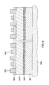
- FIG. 2 is a schematic side cross-sectional view of wafers 401 attached to a susceptor 403 , which in this embodiment may be a flat sheet or generally planar plate without windows.
- a susceptor 403 which in this embodiment may be a flat sheet or generally planar plate without windows.
- the wafers 401 are silicon and are doped to be conductive for reasons described below.
- the wafers 401 should be monocrystalline to allow the subsequent epitaxial growth of generally monocrystalline silicon. Excessively large gaps 402 may result in undesirable particle generation during subsequent processing steps.
- the lower surfaces of the wafer tiles 401 are bonded to a support substrate 403 to ensure that the upper surfaces of the wafer tiles are approximately co-planar.
- the co-planarity involves two requirements: (1) the thicknesses of wafer tiles 401 must be uniform, and (2) the thicknesses of a bond layer 404 between the back surfaces of the wafer tiles 401 and the top surface of the susceptor 403 must be uniform.
- the desire for co-planarity arises from the desire to reduce or eliminate deposition on the exposed edges of the wafer tiles at the gaps 402 .
- FIG. 3 shows a schematic side cross-sectional view of wafers 421 attached to a susceptor 425 with windows 424 between ribs 426 of the susceptor 425 providing good backside contact to the etching solution in addition to separate frontside contact to the etching solution.
- the same considerations with respect to the gaps 402 in FIG. 2 apply to gaps 422 in FIG. 3 .
- the backsides 424 of the wafers 421 are open to the etchant solution through the windows 424 , which are of the same general shape and only slightly smaller than the tiles 421 . That is, the ribs 426 form a rectangular grid and the ribs 426 support and are sealed to the peripheries of the wafers 421 .
- FIG. 4 is a schematic isometric view of wafers 508 attached in a two-dimensional array to a susceptor 502 , more generally called a support.
- the horizontally extending gaps 510 and vertically extending gaps 512 between the wafers 508 should be minimized due to the considerations discussed above with reference to FIGS. 2 and 3 .
- the susceptor 502 must be fabricated from a material which is compatible with device processing conditions such as chemical vapor deposition, plasma etching, contact formation, and such.
- Appropriate materials for the susceptor 502 may be ceramic or metal. Examples of ceramics or otherwise robust materials are alumina, aluminum nitride, silicon carbide, silicon-impregnated silicon carbide, silicon, silicon nitride, boron nitride, boron carbide, etc.
- a planar susceptor needs to be electrically conductive to the anodizing current while a windowed susceptor, though preferably conductive, may be insulating.
- the wafer tiles 508 can be held to the surface 504 of the susceptor 502 by mechanical clamps, by machined dove tail joints, by gravity, or simply by a bond to the support by field assisted bonding well known in the art.
- the bonding is needed only once for an array template used in forming a large number of solar cell arrays. Such large area device fabrication is routinely done for large displays, and even for thin film solar panels.
- the next steps in the described process for manufacturing solar panels involve the formation of a porous silicon separation layer.
- the purpose of this layer is to enable the reuse of the silicon wafer tiles in the tiled array created in FIG. 4 as described above. This reuse is possible because the solar cells do not need the full thickness of the wafer tiles, but instead they need only a partial thickness of the tiles in a preferred range of 25-50 ⁇ m as described in above section on the solar panel. Since the thickness of the mother wafer tiles is typically at least hundreds of microns (even for thin silicon wafers) and can be up to 10 mm or greater (for thick silicon blocks or laminated silicon wafers or blocks), it is possible to fabricate a substantial number of solar cell arrays from a single array of wafer tiles.
- the described processes involve the formation of a porous surface layer in the mother wafers and growth of an epitaxial layer over the porous layer, and at least partial development of the solar cell in the epitaxial layer while still attached to the array template.
- the tile array can be separated from the bulk silicon material of the source wafer tile array, leaving most of the bulk material remaining in the mother wafers to be used in the formation of additional arrays of solar cells.
- the surface of the mother wafers would be the typically rough lower surface of the cleaved porous silicon layer formed in FIGS. 5-7 , below.
- Lapping produces a surface roughness intermediate that produced by grinding and polishing.
- Lapping involves rotating a planar surface of a disk, often metal and perhaps textured or grooved, against the surface with typically a lapping powder being disposed between the disk and the surface. It typically produces an RMS surface roughness of 50 to 100 nm.
- Grinding involves rotating the circular face of an abrasive grinding wheel against the workpiece surface. It typically produces an RMS surface roughness of greater than 100 nm.
- Polishing is similar to lapping but uses a softer polishing powder and a typically softer non-metallic polishing pad to typically produce a surface roughness of less than 50 nm.
- the rougher ground silicon surface is rougher than a lapped surface and may enable even easier peeling, but the rougher ground surface may lead to too many defects in the epitaxial layer grown thereon.
- a polished silicon surface may be nearly free of surface flaws, but we believe that the porous layer formed thereon will be relatively more difficult to detach.
- FIG. 5 A schematic isometric view of an anodic etcher capable of simultaneously etching multiplicities of wafers attached in a vertical orientation to each of a plurality of susceptors is shown in FIG. 5 .
- the anodic etcher 601 contains within dielectric tank walls two electrodes 604 , 605 preferably formed of platinum and electrically connected to a power supply 606 by respective wires 606 , 607 .
- One or more susceptors 610 are removably immersed in the electro-etching solution 603 , typically hydrofluoric acid (HF). If the windowed susceptor shown in FIG.
- both the front and back sides of the wafer tiles 611 will be exposed to the electrolytic solution, but the wafer tiles 611 need to be sealed to the ribs 425 of the windowed susceptor 426 to electrically isolate the electrolytic solutions at the front and back.
- a conductive windowed susceptor is preferred for anodization although it presents some challenges.
- one or more holes through an otherwise planar susceptor for each wafer provides liquid contact to the wafers.
- the non-windowed susceptor shown in FIG. 2 may be used if the susceptor is electrically conductive and in good electrical contact with the source wafers affixed thereto.
- the edges of the susceptors 610 form a seal against the internal walls of the anodization tank 601 interrupting the electrical path of the electrolytic solution and the etching solution does not extend over the top of the susceptors 610 , then the susceptors 610 and their attached wafer 611 will essentially form electrodes in a serial arrangement for the anodic etching process and not require actual electrical connections of the wafers or susceptors to the power supply 606 .
- the liquid backside contact is advantageous in ensuring uniform etching across the surfaces of the wafers 611 .
- a positive bias on the fronts of the wafers relative to their backs only the front surfaces of the wafers 611 will react with the HF solution 603 as is familiar to those skilled in the art.
- a top surface of the electrolytic solution 603 typically hydrofluoric acid, is below the tops of the susceptors 610 to ensure that each susceptor 610 and attached wafers 611 form a separate electrode in the electro-etching circuit.
- Etching a large array of silicon wafers to produce the needed porous layer structures requires uniform anodic current distribution across individual wafers, and between all wafers in the array. Further, the silicon wafers need to be conductive to the anodization current, for example, having an electrical conductivity in the range of 0.001 to 0.1 ohm-cm, 0.02 ohm-cm being a convenient value. Either p-type or n-type silicon wafers can be anodized. Discrete metal electrode contacts for either the anode or cathode do not yield the desired level of uniformity in etching, leading to non-uniformities even within single wafers.
- the support substrate needs to be in good electrical contact with the wafer, and should be a good electrical conductor itself.
- the susceptor may have openings or slots to allow for the electrolyte to directly contact the wafer back sides.
- An embodiment of an anodization tank shown in a schematic side cross-sectional view of FIG. 6 of the anodic etcher 601 of FIG. 5 can contain up to at least five susceptors 610 , each having a multiplicity of wafers 611 affixed thereto.
- the manufacturing sequences described in FIGS. 20 and 21 would employ such an electro-etching arrangement.
- An anodic etcher 621 illustrated in the schematic sectioned isometric view of FIG. 7 is capable of simultaneously etching a number of wafers 631 , each attached in a vertical orientation to a support frame 630 .
- these wafers are not yet detachably attached to a susceptor, and are, instead, attached to the support frames 630 , which form seals against the internal walls of the etch chamber 621 .
- Either round or square wafers 631 may be attached to the support frames 630 mounted within etch chamber 621 , which can be much smaller than the etch chamber 601 of FIGS. 5 and 6 .
- Electrodes 624 , 625 are electrically connected to a power supply 628 though respective wires 626 , 627 .
- the top surface of the etch solution 623 typically hydrofluoric acid, filled into the anodization tank 621 should be below the tops of the support frames 630 and the support frames 630 should be sealed to the sidewalls of the anodization tank 621 to isolate the cells of the serial electro-etching apparatus to ensure that each wafer forms an electrode in the etching circuit.
- a graded porosity has the advantage that the low porosity silicon layer may be easier to thermally smooth in the respective steps 203 , 223 , 243 , and 263 in FIGS. 20-23 ) prior to epitaxial growth of the n-type and p-type layers in the PV cells.
- the electro-etching process for generating a high porosity film in the wafers has different etch parameters than the electro-etching process for generating a low porosity film, however the configuration of the electro-etching apparatus as shown in FIGS. 5-7 can be used for both cases and for some types of grading one electro-etching apparatus may serially anodize both sub-layers.
- the ability to modulate porosity by changing etch chemistry, etch current, or both has been an important innovation
- the wafer tile arrays After the electro-etching processes illustrated in FIGS. 5 and 6 to produce the porous silicon surface layer, the wafer tile arrays, still attached to the susceptors 610 , are removed from the anodization tank 601 for subsequent processing using various standard semiconductor processes, starting with thermal smoothing followed by epitaxial deposition of silicon in a reactor.
- the wafers In the case of the anodizaton tank 621 of FIG. 7 , the wafers are typically remounted onto a susceptor carrying a closely packed array of solar wafer tiles including the mother wafers using the mounting methods described for susceptor 502 of FIG. 4 .
- planar susceptor of FIG. 2 is more easily used in a radiantly heated epitaxial reactor.
- the exposed surface of the anodized porous silicon layer is advantageously smoothed to promote epitaxial growth of silicon on the porous layer.
- the smoothing may be performed as described in the aforecited Ser. No. 12/290,588 by annealing the mother wafer(s) in a hydrogen ambient at generally atmospheric pressure for a time of about 10 minutes and a temperature of 900 C. or higher.
- the thermal smoothing can be done in conventional thermal processing oven, advantageously it is done when the mother wafers are mounted on susceptors, which are assembled into a wafer sleeve and thermally smoothed as a group, for example, using the radiantly heated epitaxial reactor described next.
- the epitaxial reactor for depositing the silicon onto the conditioned surfaces of the source wafer template array has been described in detail by Sivaramakrishnan et al. in co-pending U.S. patent application Ser. No. 12/392,448, filed Feb. 26, 2008 and incorporated herein by reference.
- the epitaxial reactor has been designed to rapidly and simultaneously deposit silicon onto a large number of wafers by a thermal chemical vapor deposition (CVD) process using radiant lamps.
- CVD thermal chemical vapor deposition
- multiple wafers 720 are held on the interior surfaces of each of two susceptors 706 facing each other at close distance to confine the heat and the reacting gases close to the wafer surfaces.
- the assembly of two susceptors 706 and two end caps 701 forms a “wafer sleeve” with two open ends and having a relatively small interior volume.
- the two end caps 701 each have a tongue 702 which fits between the two susceptors 706 , defining the spacings between the susceptors 706 at each susceptor edge.
- the flow direction of the reactor gases flowing though the wafer sleeve between its open ends is reversed frequently in what is called “cross-flow processing” to avoid gas depletion at middle regions of the susceptor, thereby improving deposition thickness and resistivity uniformity.
- cross-flow processing provides for excellent uniformity in temperature and reactive gas supply, ensuring highly uniform epitaxial silicon deposition.
- the reactor may be equipped with two or three reaction chambers in series, the first one to preheat the succeptor, the second for the deposition of the epitaxial silicon, and the last one to cool the succeptor. Dopant species can be bled into the reaction chamber, as necessary, to form as grown junctions. This reactor arrangement greatly enhances the throughput of the epitaxial reactor.
- Important advantages of the epitaxial reactor and process of this invention are: (1) a large-area vertical reactor with low volume to minimize gas cost and footprint; (2) a high-growth rate (2-10 ⁇ m/min) in the mass transport regime at temperatures exceeding 1000 C.; (3) multiple wafer processing on two or more wafer susceptors that are processed simultaneously since the gases and incandescent heating lamp array is shared for two susceptors within the wafer sleeve; (4) lamp based heating for fast temperature cycling to enable a quick process sequence; and (5) efficient flow distribution for the silicon precursor trichlorosilane (TCS) with silicon conversion rates exceeding 50%.
- TCS trichlorosilane
- the substrates carrying the wafer arrays will constitute the susceptor.
- the gas flow is advantageously aligned with the shorter dimension of the solar array, again to minimize gas depletion effects in the center.
- FIG. 9 is a schematic side cross-sectional view of two mother or source wafers 801 attached to a susceptor 800 with PV cell structures epitaxially formed on the upper surfaces of each mother wafer 801 in the epitaxial reactor.
- Each PV cell includes at least one p-type layer 803 and at least one n-type layer epitaxially formed on top of a porous silicon layer 802 formed using the anodic etching process discussed in FIGS. 5-7 . Note that if the anodic etching apparatus of FIGS. 5 and 6 is used, the porous silicon layer 802 will have been formed after attachment of the mother wafers 801 to the susceptor 800 ; but if the electro-etching apparatus of FIG. 7 is used, the porous silicon layer 802 will have been formed prior to attachment of the mother wafer 801 to the susceptor 800 .
- the growth process for the PV cells on the different mother wafers 801 proceeds in parallel using the vertical epitaxial reactor described above.
- an n-doped layer 804 is epitaxially deposited. The order of the p-type and n-type layers can be reversed if desired.
- Epitaxial silicon can be deposited with as-grown p-n junctions by adding suitable dopants during portions of the silicon deposition process, as shown in the two co-pending patent applications of K. V. Ravi and the co-pending patent application of Sivaramakrishna. Such junctions may also be formed after epitaxial growth by well known dopant thermal diffusion methods.
- the cell fabrication steps, including the contact formation methods described here are for examples only.
- the susceptor and attached mother wafers are then removed from the epitaxial reactor and further processed for the formation of contacts and surface layers and separation from the template array and final processing. Depending upon the type of cell structure, some of the contact processing may be performed after the cell array has been removed from the template array.
- CMOS complementary metal-oxide-semiconductor
- HIT double hetero junction
- IBC integrated backside contact
- the contacts on one side of the cell are formed on cells of the array while still attached to the mother wafers on the susceptor while the contacts on the other opposite side are formed after the entire array has been glued to a glass layer and subsequently separated from the mother wafers.
- the encapsulants used to bond the array to the backing sheet will limit the processing temperature for the second side metal contact formation.
- the IBC cells are well suited for the solar array fabrication of this invention because all of the contact fingers can be fabricated on the cells prior to array detachment. In this case, the only remaining processes required to be performed on the front side of the array are cleaning, texturing, low temperature depositions of passivation and anti-reflection layers, after the solar array is separated from the mother wafers attached to the susceptor.
- the contacts can be fabricated using deposited thin films, such as TiPdAg, AlTiWCu—CuSn patterned using shadow or resist masks or can be formed using screen printed silver-based pastes. The latter require firing at elevated temperatures to sinter the silver and to obtain good electrical contact and adhesion to the wafer. It is worthwhile to note here that the infrastructure already exists to fabricate metal interconnect patterns on large form factor substrates in the printed circuit board and flat panel display industries.
- openings in the n-type layer 804 are made, enabling p-layer connections 805 to contact the p-type layer 803 without shorting the n-type layer 804 .
- n-layer connections 806 are made to the n-layer 804 . Details of a process sequence for backside contact wafer fabrication are provided in U.S. patent application Ser. No. 12/290,588.
- Another aspect of the invention includes some module fabrication steps to achieve simultaneous separation of the epitaxial solar array from the source wafer template array.
- a semi-rigid that is, somewhat flexible, glue layer such as ethylene vinyl acetate, EVA, commonly used in solar module encapsulation,
- EVA ethylene vinyl acetate
- the glue layer unites the cell array into a single somewhat flexible and peelable entity.
- the glue layer is then used for attaching a rigid module support layer, such a glass or Tedlar, either before or after array separation.
- a glue layer 807 and a module support layer 808 are added to the structure shown in FIG. 9 .
- the glue layer 807 and module support layer 808 are array-level features for module support. Note that the glue layer 807 not only covers the PV cells and the PV cell contacts 805 , 806 , but may also flow down between the p-type and n-type layers 803 , 804 of neighboring PV cells and between neighboring mother wafers 801 , which are still attached to the susceptor 800 .
- the illustrated top surface including the glue layer 806 and module support layer 808 will become the backside of the complete PV cells.
- the glue layer 807 flows around the p-n junction to hermetically encapsulate the solar cell.
- the module support layer 808 which may be formed of glass, is optional and is usually different from the final strengthening layer applied after defoliation. If it is used, it should be relatively flexible to permit defoliation by progressive peeling. In general, the glue layer 807 is less rigid than the soon to be described handle layer and than the support layer 808 .
- the individual cells may be ‘conditioned’ to easily peel or separate from the porous silicon layer.
- This conditioning starts with proper surface preparation of the source wafers prior to anodization assuring a preferred structure for the porous layer stack, and the overall uniformity of this stack within wafers, wafer-to-wafer, and array-to-array.
- This conditioning may also involve edge grinding or laser removal of the epitaxial layer that wraps around the edge of the source wafers.
- Another aid for easy array separation with the required high yields is to minimize the possibility of breakage of the thin epitaxial cells during the separation process.
- the polymeric glue encapsulation and the rigid or semi rigid substrate backing spanning the entire array may adequately assure this.
- Another way to assure that the individual cells do not break during separation involves forming a rigid ‘handling layer’ on the individual cells, which serves as a rigid backbone for the thin cells.
- a preferred low cost approach is to fabricate such a handling layer in situ from deposited or dispensed precursors on top of the epitaxial cells. If the cell contacts are made by thin film methods, this rigid handling layer is made from polymeric materials from precursors.
- suitable polymeric materials include epoxies, polyurethanes, cyanate resins, preferably filled with inert fillers such as fumed silica, cordierite inorganic glass powders or fibers.
- Asphalt and similar materials may also be suitable for forming the handling layer.
- the precursors, in the form of viscous solutions, are dispensed on top of the finished cells, and cured, as necessary to set and become rigid.
- the handling layer is formed by fusing a suitable glass, ceramic, or cermet handling layer onto the individual cells.
- a preferred approach is to deposit a slurry of the precursor powders on the epitaxial cells and sinter them at high temperatures to flow and adhere to the epitaxial cells. It is advantageous to deposit the powder precursors on top of the screen printed silver pattern and to sinter both together.
- the material of the handling layer materials should be chosen to conformably coat and adhere well to the cell surface, including any metallization thereon and to have a coefficient of thermal expansion (CTE) close to that of silicon.
- suitable insulating materials useful for such in situ substrate fabrication include certain vitreous glasses (examples Pyrex, Corning glass 7070), glass and ceramic mixtures which together fire at the required temperatures while giving rise to a rigid body with a CTE matched to silicon, devitrifiable glasses which sinter and crystallize simultaneously upon firing (examples include certain lithium alumino-silicate or magnesium alumino-silicate glasses, and mullite, 3Al 2 O 3 -2SiO 2 ).
- Cermet compositions that can be used for this application are Si—SiC and Al—SiC. While the handling layer is intended to strengthen the epitaxial silicon cell, its attachment, or fabrication thereto, it also pre-disposes the cells for easy separation due to the small, but inevitable CTE mismatch stress between the handling layer and silicon. The cells provided with individual handles still need module encapsulation with semi-rigid EVA-type adhesives, to unite them into an array before or after array separation.
- FIG. 10 An alternative process to that shown in FIG. 10 first deposits the precursor for a handling layer on the structure of FIG. 9 , followed by heating to simultaneously sinter the contacts 805 , 806 and to convert the handling layer precursor into a handling layer 809 , illustrated in FIG. 11 , separately covering each of the PV cells in the array. Due to surface tension and the deposition of the handling layer precursor away from the edges of the n-type layer 804 , the handling layers 809 do not extend between neighboring PV cells but instead leave gaps 808 so that the rigid handling layer 809 does not prevent bending between cells during peeling. This difference should be considered because the stiffness of the handling layer, if it were to bridge the PV cells, would make exfoliation difficult as shown in FIGS. 14-19 .
- the handling layer is a cell-level feature, which may be formed in situ on the epitaxial silicon to reinforce it and to dispose it towards easy peeling.
- the individual cells can be tested prior to separation by using either a cell-size or an array-size probe head. It should be recognized that the testing at this stage is limited to measuring some cell electrical characteristics and not directly cell performance. With a database of these characteristics, defective cells may be identified and replaced with single cells from storage, prior to encapsulation. Full cell and array level testing can only be done after the array separation and surface finishing and cell completion steps on the peeled surface.
- the glue layer 810 and the support layer 811 are attached to the upper surfaces of the handling layers 809 , which will become the backsides of the completed PV cells.
- the glue layer 810 may flow down in the gap 808 between the handling layers 809 and then between the PV cells and mother wafers 801 . If the glue layer 810 flows at least past the solar cell layer 803 , it provides side encapsulation for the semiconductor layers and their junctions. The relative flexibility of the glue layer 810 does not prevent the bending between cell during peeling.
- the cells in the array can be electrically connected to each other, i.e. strung together, in the required configuration by spot soldering a tin-coated copper strip 1550 to tabs (contacts) on the cells formed as part of the cell interconnections, prior to encapsulation.
- a large number ( 72 in this example) of PV cells 1558 may be been grown on top of the X-Y array of mother wafers 508 of FIG. 4 .
- Japanese laid-open patent application 7-302889 describes a method bonding a second silicon wafer to the epitaxial layer, bonding plates to the silicon wafers, and then separating the plates by force from each other such that the epitaxial layer remains attached to the support substrate.
- Japanese laid-open patent application 8-21345 is similar to the above but performs the separation after forming the p-n solar cell junction thereon while both the parent substrate and the support substrates are bonded to jigs with adhesive.
- the support substrates can be quartz or metal.
- Mizutani et al. use a curved surface of a support substrate to peel the epitaxial film away from the growth substrate while the latter is secured on a support member by means of vacuum chuck, electrostatic chuck, or by mechanical clamps.
- a flexible polymer film which could be self-adhering film or tape, is bonded to the epitaxial film, with an edge extending outwardly from the substrate serves to grip the film to initiate the peeling action.
- the edge of the film is then secured to drum-shaped, or blotter-shaped (semi-circle) support with a prescribed radius of curvature designed to peel the epitaxial film gently as the support member is rotated.
- the holding and peeling of the semiconductor film can be, by vacuum suction, electrostatic suction, mechanical claws, and such.
- FIGS. 15 and 18 are schematic side cross-sectional views of the separation of the highly porous silicon layers anodically etched in either the anodization apparatus of FIGS. 5 and 6 or that of FIG. 7 .
- the peeling process typically separates the porous silicon layer in each of the wafers into two layers: (1) a lower layer attached to the upper surface of the mother wafer; and (2) an upper layer attached to the PV cell structure.
- the surfaces of these two layers will both be physically and optically rough due to the separation process. This optical roughness can potentially increase the light collection efficiency of the solar cell since the upper layer attached to the PV cell structure forms the front surface of the final solar cell array.
- the separation process for the porous silicon film may be accomplished in a number of other ways, as illustrated in FIGS. 14-19 below.
- an array of electrode strips are placed on a flexible polymer film bonded to the epitaxial silicon layer and acts as additionally as a dielectric layer.
- the flexible film may be the previously described glue layer.
- the potential is first applied between the outermost electrode, which is placed on the edge of the flexible film, and the grounded silicon source substrate. This localizes the electrostatic gripping to roughly the area covered by the electrode. As this electrode is lifted, it will apply an upward force on the epitaxial silicon layer directly underneath. When a sufficient upward force is applied, it will initiate peeling at the edge between the epitaxial layer and the source substrate.
- the next electrode in the array is activated and pulled up, to propagate the peel further.
- the peel having been already initiated at the edge, the force required to propagate the peel to this second region will be much less.
- This action is carried out across the entire array of electrode strips to complete the peeling of the epitaxial layer as the same actions are initiated on the electrode strip next to the electrode strips already peeled.
- a mechanical stop can be placed on the electrode lift pins.
- they can be tied to a tie bar made of a suitable dielectric such as a structural plastics or a ceramic such as alumina.
- an array of wafer tiles 3016 is encapsulated with a semi-rigid but somewhat flexible glue layer 3012 and clamped overhead to a segmented electrostatic chuck prior to separation of the highly porous silicon films 3010 formed in either the anodization tank of FIGS. 5 and 6 or that of FIG. 7 .
- the segmented electrostatic chuck includes a plurality of clamping strips 70 - 77 enclosed and electrically isolated by respective dielectric films 80 - 87 .
- the clamping strips 70 - 77 are juxtaposed to different ones of the wafer tiles 3016 across the semi-rigid glue layer 3012 and, as also shown along section line A-A in the top view of FIG. 16 .
- multiple clamping strips are juxtaposed to each of the wafer tiles 3016 so that each tile is subjected to a gradual peeling including bending of the separate wafer tiles 3016 . Peeling action may be initiated from the left in the illustration of FIG. 14 , then progressively moving to the right.
- An electrostatic clamping power supply 3024 preferably a DC power supply, is connected through a first electrical connection 3006 to either mother wafers 3002 or a substrate support 3025 , which may be the previously described susceptor.
- the substrate support 3025 may be at ground potential as shown in the figure; however, another potential may be used for proper clamping operation.
- the other output of the power supply 3024 is connected through a second electrical connection 3004 to a series of switches 50 - 57 as shown, all but the switch 50 separating different ones of the electrostatic clamping strips 70 - 77 . When switch 50 is closed as shown, the clamping voltage is applied to the first electrostatic clamping strip 70 through a first electrical connection 60 .
- the clamping voltage is applied to the second electrostatic clamping strip 71 through a second electrical connection 61 .
- the clamping voltage is sequentially applied to the remaining serially arranged electrostatic clamping strips 72 - 77 through electrical connections 62 - 67 .
- the electrostatic clamping strips 70 - 77 are applied to the top of the flexible film 3012 on top of multiple solar cells 3016 .
- Porous separation layers 3010 which may be formed in either the anodization tank of FIGS. 5 and 6 or that of FIG. 7 , separate the respective solar cells 3016 and the mother wafers 3002 .
- Each of the electrostatic clamping strips 70 - 77 is attached to a mechanical actuator (not shown) capable of moving clamping strips 70 - 77 individually in a vertical up-down motion 3018 illustrated for the first clamping strip 70 in the side cross-sectional view of FIG. 15 .
- the figure shows the initiation of peeling of the solar cells 3016 from the substrates 3002 by separation (exfoliation) across the porous silicon layers 3010 for the portion of the solar cell 3016 underlying the first electrostatic clamping strip 70 , which had been activated by the closing of by the closing of the first switch 50 At this point, the remaining electrostatic clamping strips 71 - 77 are not yet activated, that is, are not yet clamping the associated solar cell 3016 since the switches 51 - 57 remain open.
- Upwards arrow 3108 represents a vertical pulling motion by a mechanical actuator (not shown) attached to electrostatic clamping strip 70 .
- the leftmost solar cell(s) Due to the electrostatic clamping action between the first clamping strip 70 and the leftmost solar cell(s) in the array of solar cells 3016 , when the first clamping strip 70 is pulled up by the actuator, the leftmost solar cell(s) are also pulled up as shown by a separated (peeled or exfoliated) portion 3104 of the porous layer 3010 and the continuous flexible layer 3012 is bent between the attached and detached solar cells 3016 .
- the remaining electrostatic clamping strips 71 - 77 are sequentially actuated in the sequence 71 , 72 , . . . 77 by the sequential closing of the switches 51 - 57 in the sequence 51 , 52 , . . . 57 .
- the essential point of this aspect of the invention is the application of pulling force locally at an edge of the epitaxial film to grip and pull the edge of the film at its edge and thereafter to sequentially create similar forces and separations on adjacent areas of the film until the entire epitaxial layer is separated from the source wafer at the location of the separation layer.
- the idea transcends any specific means for creating these actions, such as specific electrode arrangements, the gripping means, or of the means for lifting the gripped film and such which results in a rolling motion across the array of solar cells.
- the entire peeling action may be accomplished by vacuum suction.
- the vacuum suction is applied locally through an array of vacuum ‘strips’ placed pressing on the film, starting from the outermost strips and working progressively across the others to the other side.
- the level of vacuum is designed to separate and lift the film from the source substrate. As this action is translated across the film, the separation proceeds in a predictable manner until the entire film is peeled and separated from the source wafer.
- the sequential activation of the vacuum strips in the array can be regulated by providing a feedback loop using fluidic devices and such, and thereby made to be reliable and reproducible for peeling epitaxial silicon layers from porous or other separation layers of mother wafers.
- a progressive vacuum chucking system is illustrated in the side cross-sectional view of FIG. 17 , in which an array of wafer tiles 3306 need not be covered by a flexible film but are directly clamped to a segmented vacuum chuck prior to separation of the highly porous film formed in either of previously described anodization tanks.
- vacuum peeling action is initiated from the left, then moving to the right.
- a vacuum line 3308 connects a vacuum pump (not shown) to a manifold 3302 , creating a vacuum within the manifold 3302 .
- Multiple valve actuators 3370 - 3377 enable the opening and closing of respective valves 3380 - 3387 .
- FIG. 17 the first valve 3380 is shown open, and the remaining valves 3381 - 3387 are shown closed. Opening of the first valve 3380 causes a vacuum to be formed within a first vacuum clamping strip 90 forming the first segment of the segmented vacuum clamp.
- a first flexible hose connects the first vacuum clamping strip 90 to the first valve 3380 to selectively supply vacuum to it.
- the other valves 3381 - 3387 are similarly connected to the vacuum clamping strips 91 - 97 through respective flexible tubes 3391 - 3397 .
- FIG. 19 is a top view through cross-section B-B of FIG. 17 of the eight vacuum clamping strips 90 - 97 and flexible tubes 3390 - 3397 in FIGS. 17 and 18 .
- the eight vacuum clamping strips 90 - 97 attach directly to the array of solar cells 3306 of FIG. 17 .
- Porous separation layers 3310 separate the solar cells 3306 and mother wafers 3302 held on a support 3307 .
- Each of the vacuum clamping strips 90 - 97 is activated by respective vacuum actuators 3370 , 3371 , . . . 3377 and is attached to one or more mechanical actuators (not shown) capable of moving clamping strips 90 - 97 individually in a vertical up-down motion, as shown in FIG. 18 .
- a semi-rigid glue layer may be positioned between the vacuum clamping strips 90 - 97 and the solar cells 3306 , similar to the arrangement of FIGS. 14 and 15 .
- FIG. 18 illustrates the initiation of peeling of the solar cells 3306 (not covered by a semi-rigid glue layer in this illustration) from the support substrate 3302 by separation of a porous layer 3310 .
- Upwards arrow 3389 represents a vertical pulling motion of a mechanical actuator (not shown) attached to the first vacuum clamping strip 90 . Due to the vacuum clamping action between the first vacuum clamping strip 90 and the leftmost solar cell(s) in solar cell array 3306 , when the first vacuum strip 90 is pulled up by the actuator, the leftmost solar cell(s) are also pulled up as shown by separation (peeling) 3404 . The remaining vacuum clamping strips 91 - 97 are actuated in the sequence 91 , 92 , .
- FIGS. 20-23 Four alternative sequences are illustrated in FIGS. 20-23 for the first part of the overall manufacturing process and two alternative sequences are illustrated in FIGS. 24 and 25 for the last part of the manufacturing process. Any of the sequences described in FIGS. 20-23 may be used with either of the sequences in FIGS. 24 and 25 .
- the flow chart of FIG. 20 illustrates a first embodiment of the first part of a manufacturing process for solar panels.
- a number of mother wafers are attached to a susceptor, as described in FIGS. 2-4 above.
- the number of mother wafers may correspond to the full number of PV wafers in a solar panel or a fraction of the full number.
- porous silicon layers are formed on the surfaces of all the mother wafers using an anodization system such as that shown in FIGS. 5 and 6 .
- One or more susceptors are then mounted into a wafer sleeve as shown in FIG. 8 , which is designed to interface with an epitaxial reactor such as that described in U.S. patent application Ser. No. 12/392,448.
- step 203 the wafer sleeve comprising one or more susceptors loaded with mother wafers is heated to thermally smooth the surfaces of the porous silicon layers.
- This thermal smoothing process provides a sufficiently smooth and crystalline surface on which to grow the n-type and p-type layers comprising the PV cells.
- step 204 epitaxial deposition processes fabricate the PV cells on top of the smoothed porous silicon layer.
- the wafer sleeve is disassembled to enable, in the second part of step 204 , contact holes to be formed to the n-type and p-type layers of the cells.
- step 205 thin film contacts are then formed on the surfaces of all the wafers attached to the respective susceptor.
- step 206 the precursor for the handling layer is deposited on the wafer surfaces on the sides which correspond to what will be the back sides of the completed PV cells.
- step 207 the handling layer is formed by heating the handling layer precursor material deposited in step 206 .
- the handling layer precursor of step 206 may be omitted.
- step 208 metal stringers are then soldered or otherwise attached electrically to the contacts on the wafers as shown for the structure in FIG. 13 .
- Arrow 209 indicates that the solar panel fabrication process continues with the process of either FIG. 24 or 25 , depending on the type of PV cells used (see below).
- the flow chart of FIG. 21 illustrates a second embodiment of the first part of a manufacturing process for solar panels.
- a number of mother wafers are attached to a susceptor, as described above for FIGS. 2-4 .
- the number of mother wafers may correspond to the full number of PV wafers in a solar panel or a fraction of the full number.
- porous silicon layers are formed on the surfaces of all the mother wafers using an anodization system such as that shown in FIGS. 5 and 6 .
- One or more susceptors are then assembled into a wafer sleeve as shown in FIG. 8 , which is designed to interface with an epitaxial reactor such as that described in U.S. patent application Ser. No. 12/392,448.
- step 223 the wafer sleeve comprising one or more susceptors loaded with mother wafers is then heated to thermally smooth the surfaces of the porous silicon layers.
- This thermal smoothing process provides a sufficiently smooth and crystalline surface on which to grow the n-type and p-type layers comprising the PV cells.
- step 224 epitaxial deposition processes are used to fabricate the PV cells on top of the smoothed porous silicon layer and contact holes are formed to the n-type and p-type layers of the cells.
- the wafer sleeve is disassembled to enable in step 225 thick film contacts to be screen printed on the surfaces of all the wafers attached to the susceptors.
- the screen printing process deposits thick film contacts not requiring the later attachment of metal stringers.
- step 226 the precursor for the handling layer is deposited on the wafer surfaces, on the sides which correspond to what will be the back sides of the completed PV cells.
- step 227 the handling layer is formed by heating the handling layer precursor material. Simultaneously, the metal contacts to the wafers are sintered to make good ohmic contact.
- the handling layer precursor may be omitted, in which case step 227 corresponds solely to the sintering of the metal contacts.
- Arrow 228 indicates that the solar panel fabrication process continues with the process of either FIG. 24 or 25 , depending on the type of PV cells used.
- the flow chart of FIG. 21 illustrates a third embodiment of the first part of a manufacturing process for solar panels.
- step 241 porous silicon layers are first formed on the surfaces of each individual mother wafer using an anodization system such as that shown in FIG. 7 .
- a number of mother wafers are attached to a susceptor in step 242 , as described above for FIGS. 2-4 .
- the number of mother wafers may correspond to the full number of PV wafers in a solar panel or a fraction of the full number.
- One or more susceptors are then assembled into a wafer sleeve as shown in FIG. 8 , which is designed to operate in an epitaxial reactor.
- the wafer sleeve comprising one or more susceptors loaded with mother wafers is then heated in step 243 to thermally smooth the surfaces of the porous silicon layers.
- This thermal smoothing process provides a sufficiently smooth and crystalline surface on which to grow the n-type and p-type layers forming the PV cells.
- step 244 epitaxial deposition processes are used to fabricate the PV cells on top of the smoothed porous silicon layer, and contact holes are formed to the n-type and p-type layers of the cells.
- the wafer sleeve is disassembled to enable, in step 245 , thin film contacts to be formed on the surfaces of all the wafers attached to the respective susceptors.
- the precursor for the handling layer is deposited on the wafer surfaces, on sides which correspond to what will be the back sides of the completed PV cells.
- the handling layer is formed by heating the handling layer precursor material. In a variation on this processing sequence, the handling layer precursor may be omitted.
- metal stringers are then soldered or otherwise attached electrically to the contacts on the wafers as shown in FIG. 13 .
- Arrow 249 indicates that the solar panel fabrication process continues with the process of either FIG. 24 or 25 , depending on the type of PV cells used.
- the flow chart of FIG. 23 illustrates a fourth embodiment of the first part of a manufacturing process for solar panels.
- step 261 porous silicon layers are first formed on the surfaces of each individual mother wafer using an anodization system such as that shown in FIG. 7 .
- step 262 a number of mother wafers are attached to a susceptor, as described above for FIGS. 2-4 .
- the number of mother wafers may correspond to the full number of PV wafers in a solar panel or a fraction of the full number.
- One or more susceptors are then assembled into a wafer sleeve as shown in FIG. 8 , which is designed to operate with an epitaxial reactor such as that previously described.
- step 263 the wafer sleeve comprising one or more susceptors loaded with mother wafers is then heated to thermally smooth the surfaces of the porous silicon layers.
- This thermal smoothing process provides a sufficiently smooth and crystalline surface on which to grow the n-type and p-type layers forming the PV cells.
- step 264 epitaxial deposition processes are used to fabricate the PV cells on top of the smoothed porous silicon layer and contact holes are formed to the n-type and p-type layers of the cells.
- the wafer sleeve is disassembled to enable, in step 265 , thick film contacts to be screen printed 265 on the surfaces of all the wafers attached to the susceptors.
- the screen printing process deposits thick film contacts not requiring the later attachment of metal stringers.
- step 266 the precursor for the handling layer is deposited on the wafer surfaces, on sides which correspond to what will be the back sides of the completed PV cells.
- step 267 the handling layer is formed by heating the handling layer precursor material. Simultaneously, the metal contacts to the wafers are sintered to make good ohmic contact.
- the handling layer precursor of step 266 may be omitted, in which case step 267 corresponds solely to the sintering of the metal contacts.
- Arrow 268 indicates that the solar panel fabrication process continues with the process of either FIG. 24 or 25 , depending on the type of PV cells used.
- one of two processes may be used for the second part depending on the type of partial cell completed in the first part.
- the flow chart of FIG. 24 illustrates a first embodiment for the second part of the manufacturing processing for completing a solar panel in the case where backside contact PV cells were fabricated in the first part of the manufacturing process.
- the array of wafers containing the PV cell structures on their upper surfaces are still attached to the susceptor at this point.
- a glue layer such as EVA
- EVA is laid across the full array of wafers with a glass layer on top of it. If a handling layer was formed in one of the manufacturing sequences illustrated in FIGS. 21-23 , then the EVA layer is on top of the handling layer, and in step 272 , the EVA bonds the glass layer to the top surface of the handling layer as shown in FIG. 12 . In the alternative case where the handling layer was not formed on top of the wafers, in step 272 , the EVA bonds the glass layer to the top surface of the PV cells as shown in FIG. 10 .
- step 273 the susceptor mounting the mother wafers and PV cells and the EVA and glass layers is placed in an exfoliation system such as those illustrated in FIGS. 14-19 .
- the exfoliation process leaves a portion of the porous silicon layer remaining on the top surfaces of the PV cells which are attached to the EVA and glass layer.
- This remnant porous layer is removed in step 274 by conventional etch processes as is familiar to those skilled in the art.
- step 275 the frontsides of the wafers are texture etched to form a surface which, when combined with the anti-reflective coating deposited in step 276 , minimizes the reflection of light and thus improves the light collection efficiency for the solar panel.
- the flow chart of FIG. 24 illustrates a second embodiment for the second part of the manufacturing process for completing a solar panel in the case where both frontside and backside contacts were fabricated in first part of the manufacturing process.
- the array of wafers containing the PV cell structures on their upper surfaces is still attached to the susceptor.
- thin film contacts are deposited on the exposed frontsides of the PV cells in the solar panel being fabricated.
- a frontside EVA layer and glass layer are laid across the panel and then thermally bonded to the frontsides of the PV cells.
- step 284 the susceptor containing the mother wafers and PV cells and the EVA and glass layers on top is placed in an exfoliation system such as those illustrated in FIGS. 14-19 .
- the exfoliation process leaves a portion of the porous silicon layer remaining on the top surfaces of the PV cells, which are attached to the EVA and glass layer.
- this remnant porous layer is removed by conventional etch processes familiar to those skilled in the art.
- step 286 the frontsides of the wafers are texture etched to form a surface which, when combined with the anti-reflective coating deposited in step 287 minimizes the reflection of light and thus improves the light collection efficiency for the solar panel.
- step 288 backside metal is deposited to form the contacts to the backsides of the PV cells in the array.
- step 289 strengthening layers are then deposited on the solar panel.
- the support substrate attached with polymer adhesive film in the proceeding descriptions serves merely to provide mechanical support and environmental protection to the solar cell.
- the contacts to the cell are first made at discrete pad or via locations, by thin or thick film means, and the bus bars or fingers are made on a polymeric film or board, prior to bonding to the epitaxial silicon layer with EVA-type of glue. These bus bars are joined electrically to the appropriate pads on the cell during the lamination process.
- Forming the interconnection patterns on the flexible polymer film or substrate, or on a large glass plate allows for it to be made offline, enabling significant reductions in the processing time on the source wafers, so that they can be made available for the next epitaxial film growth faster. Also, defective conductor patterns on the film can be repaired or sorted out, prior to placing them on the much more expensive epitaxial layers.
- the metallization for the interconnections can be made from sputtered metals such as tin coated chromium-copper, titanium-tungsten-copper, tin-coated copper, such as used in the printed wiring board industry.
- the material for joining of the cell to the bus bars has to be carefully chosen to enable good reliable ohmic contacts when cold pressed on to the contact pads or vias in the epitaxial layer.
- Examples of such metallization include silver or gold powders or flakes mixed with a polymeric material.
- the polymeric material used in the conductor pastes can be the same as the glue material used to attach the interconnection film or substrate to the epitaxial layer.
- One great advantage of fabricating the contact and interconnection layers on the flexible film is that it can carry the interconnections, not just for a single epitaxial wafer, but for an entire solar panel consisting of several such epitaxial silicon wafers, placed in a pre-arranged array configuration.
- this invention may provide an unprecedented increase in productivity.
- the invention thus provides efficient and economical manufacture of solar cell arrays in an economical small-scale set of equipment of simple design and adapted to automated operation. Thereby, inexpensive solar cell panels may be produced.
Abstract
Description
Claims (17)
Priority Applications (1)
| Application Number | Priority Date | Filing Date | Title |
|---|---|---|---|
| US13/050,807 US8900399B2 (en) | 2008-03-08 | 2011-03-17 | Integrated method and system for manufacturing monolithic panels of crystalline solar cells |
Applications Claiming Priority (3)
| Application Number | Priority Date | Filing Date | Title |
|---|---|---|---|
| US6862908P | 2008-03-08 | 2008-03-08 | |
| US12/399,248 US8030119B2 (en) | 2008-03-08 | 2009-03-06 | Integrated method and system for manufacturing monolithic panels of crystalline solar cells |
| US13/050,807 US8900399B2 (en) | 2008-03-08 | 2011-03-17 | Integrated method and system for manufacturing monolithic panels of crystalline solar cells |
Related Parent Applications (1)
| Application Number | Title | Priority Date | Filing Date |
|---|---|---|---|
| US12/399,248 Division US8030119B2 (en) | 2008-03-08 | 2009-03-06 | Integrated method and system for manufacturing monolithic panels of crystalline solar cells |
Publications (2)
| Publication Number | Publication Date |
|---|---|
| US20110300715A1 US20110300715A1 (en) | 2011-12-08 |
| US8900399B2 true US8900399B2 (en) | 2014-12-02 |
Family
ID=41054040
Family Applications (2)
| Application Number | Title | Priority Date | Filing Date |
|---|---|---|---|
| US12/399,248 Active 2029-12-10 US8030119B2 (en) | 2008-03-08 | 2009-03-06 | Integrated method and system for manufacturing monolithic panels of crystalline solar cells |
| US13/050,807 Expired - Fee Related US8900399B2 (en) | 2008-03-08 | 2011-03-17 | Integrated method and system for manufacturing monolithic panels of crystalline solar cells |
Family Applications Before (1)
| Application Number | Title | Priority Date | Filing Date |
|---|---|---|---|
| US12/399,248 Active 2029-12-10 US8030119B2 (en) | 2008-03-08 | 2009-03-06 | Integrated method and system for manufacturing monolithic panels of crystalline solar cells |
Country Status (3)
| Country | Link |
|---|---|
| US (2) | US8030119B2 (en) |
| EP (1) | EP2269230A4 (en) |
| WO (1) | WO2009114108A2 (en) |
Cited By (1)
| Publication number | Priority date | Publication date | Assignee | Title |
|---|---|---|---|---|
| US11850672B2 (en) | 2021-08-31 | 2023-12-26 | Yield Engineering Systems, Inc. | Method of using processing oven |
Families Citing this family (29)
| Publication number | Priority date | Publication date | Assignee | Title |
|---|---|---|---|---|
| EP2269230A4 (en) | 2008-03-08 | 2016-03-30 | Crystal Solar Inc | Integrated method and system for manufacturing monolithic panels of crystalline solar cells |
| US8481357B2 (en) * | 2008-03-08 | 2013-07-09 | Crystal Solar Incorporated | Thin film solar cell with ceramic handling layer |
| US20100108134A1 (en) * | 2008-10-31 | 2010-05-06 | Crystal Solar, Inc. | Thin two sided single crystal solar cell and manufacturing process thereof |
| US20100108130A1 (en) * | 2008-10-31 | 2010-05-06 | Crystal Solar, Inc. | Thin Interdigitated backside contact solar cell and manufacturing process thereof |
| US8298629B2 (en) | 2009-02-25 | 2012-10-30 | Crystal Solar Incorporated | High throughput multi-wafer epitaxial reactor |
| US8673081B2 (en) | 2009-02-25 | 2014-03-18 | Crystal Solar, Inc. | High throughput multi-wafer epitaxial reactor |
| CN101958361A (en) * | 2009-07-13 | 2011-01-26 | 无锡尚德太阳能电力有限公司 | Method for etching transparent thin-film solar cell component |
| US20110056532A1 (en) * | 2009-09-09 | 2011-03-10 | Crystal Solar, Inc. | Method for manufacturing thin crystalline solar cells pre-assembled on a panel |
| US20110253694A1 (en) * | 2010-04-16 | 2011-10-20 | Nunzio Consiglio | Radiant Heating Tile System |
| TW201210058A (en) * | 2010-05-12 | 2012-03-01 | Applied Materials Inc | Method of manufacturing crystalline silicon solar cells using epitaxial deposition |
| US20130000715A1 (en) * | 2011-03-28 | 2013-01-03 | Solexel, Inc. | Active backplane for thin silicon solar cells |
| WO2012021750A1 (en) | 2010-08-11 | 2012-02-16 | Crystal Solar, Inc. | Mwt architecture for thin si solar cells |
| WO2012024438A2 (en) * | 2010-08-17 | 2012-02-23 | EncoreSolar, Inc. | Method and apparatus for electrodepositing large area cadmium telluride thin films for solar module manufacturing |
| US8809097B1 (en) | 2010-09-22 | 2014-08-19 | Crystal Solar Incorporated | Passivated emitter rear locally patterned epitaxial solar cell |
| WO2012040688A2 (en) | 2010-09-24 | 2012-03-29 | Solexel, Inc. | High-throughput batch porous silicon manufacturing equipment design and processing methods |
| FR2969377B1 (en) * | 2010-12-16 | 2013-09-27 | St Microelectronics Crolles 2 | PROCESS FOR PRODUCING INTEGRATED CIRCUIT CHIPS |
| FR2969376B1 (en) | 2010-12-16 | 2013-09-27 | St Microelectronics Crolles 2 | PROCESS FOR PRODUCING INTEGRATED CIRCUIT CHIPS |
| US8609451B2 (en) | 2011-03-18 | 2013-12-17 | Crystal Solar Inc. | Insitu epitaxial deposition of front and back junctions in single crystal silicon solar cells |
| US9255346B2 (en) | 2011-05-27 | 2016-02-09 | Crystal Solar, Incorporated | Silicon wafers by epitaxial deposition |
| TWI558860B (en) | 2011-08-19 | 2016-11-21 | 威廉馬許萊斯大學 | Anode battery materials and methods of making the same |
| TWI473289B (en) * | 2011-09-22 | 2015-02-11 | Pinecone En Inc | Method of making a solar cell |
| CN102427101B (en) * | 2011-11-30 | 2014-05-07 | 李园 | Semiconductor structure and forming method thereof |
| US9257284B2 (en) | 2012-01-13 | 2016-02-09 | Crystal Solar, Incorporated | Silicon heterojunction solar cells |
| GB2502293A (en) * | 2012-05-22 | 2013-11-27 | Renewable Energy Corp Asa | A method for manufacturing a back contacted back junction solar cell module |
| US9559236B2 (en) * | 2014-09-24 | 2017-01-31 | Sunpower Corporation | Solar cell fabricated by simplified deposition process |
| US9620466B1 (en) * | 2015-11-30 | 2017-04-11 | Infineon Technologies Ag | Method of manufacturing an electronic device having a contact pad with partially sealed pores |
| US10490682B2 (en) | 2018-03-14 | 2019-11-26 | National Mechanical Group Corp. | Frame-less encapsulated photo-voltaic solar panel supporting solar cell modules encapsulated within multiple layers of optically-transparent epoxy-resin materials |
| CN109371383A (en) * | 2018-12-25 | 2019-02-22 | 南京爱通智能科技有限公司 | A kind of carrier suitable for ultra-large atomic layer deposition apparatus |
| CN114714156A (en) * | 2022-03-14 | 2022-07-08 | 银川隆基光伏科技有限公司 | Processing method of silicon wafer, control system, silicon wafer, solar cell and assembly of solar cell |
Citations (51)
| Publication number | Priority date | Publication date | Assignee | Title |
|---|---|---|---|---|
| US3653970A (en) | 1969-04-30 | 1972-04-04 | Nasa | Method of coating solar cell with borosilicate glass and resultant product |
| US4301324A (en) | 1978-02-06 | 1981-11-17 | International Business Machines Corporation | Glass-ceramic structures and sintered multilayer substrates thereof with circuit patterns of gold, silver or copper |
| US4445965A (en) | 1980-12-01 | 1984-05-01 | Carnegie-Mellon University | Method for making thin film cadmium telluride and related semiconductors for solar cells |
| JPS62224089A (en) | 1986-03-26 | 1987-10-02 | Hitachi Ltd | Solar cell |
| US4832755A (en) | 1987-08-11 | 1989-05-23 | The Boeing Company | Glass encapsulation of solar cell arrays to minimize voltage/plasma interaction effects in a space environment |
| US5458755A (en) | 1992-11-09 | 1995-10-17 | Canon Kabushiki Kaisha | Anodization apparatus with supporting device for substrate to be treated |
| JPH07302889A (en) | 1994-03-10 | 1995-11-14 | Canon Inc | Manufacture of semiconductor substrate |
| JPH08213645A (en) | 1995-02-02 | 1996-08-20 | Sony Corp | Method of separating element formation layer from base body |
| US5834840A (en) | 1995-05-25 | 1998-11-10 | Massachusetts Institute Of Technology | Net-shape ceramic processing for electronic devices and packages |
| US5951833A (en) * | 1996-11-28 | 1999-09-14 | Canon Kabushiki Kaisha | Anodizing apparatus |
| US6143629A (en) | 1998-09-04 | 2000-11-07 | Canon Kabushiki Kaisha | Process for producing semiconductor substrate |
| US6190937B1 (en) | 1996-12-27 | 2001-02-20 | Canon Kabushiki Kaisha | Method of producing semiconductor member and method of producing solar cell |
| US6211038B1 (en) | 1997-03-27 | 2001-04-03 | Canon Kabushiki Kaisha | Semiconductor device, and method for manufacturing the same |
| JP2001158680A (en) | 1999-11-30 | 2001-06-12 | Ibiden Co Ltd | Silicon carbide-metal complex, method for producing the same, member for wafer-polishing device and table for wafer-polishing device |
| US6258666B1 (en) | 1998-06-18 | 2001-07-10 | Canon Kabushiki Kaisha | Method of producing semiconductor thin film and method of producing solar cell using same |
| US6331208B1 (en) | 1998-05-15 | 2001-12-18 | Canon Kabushiki Kaisha | Process for producing solar cell, process for producing thin-film semiconductor, process for separating thin-film semiconductor, and process for forming semiconductor |
| US6428620B1 (en) | 1997-12-26 | 2002-08-06 | Canon Kabushiki Kaisha | Substrate processing method and apparatus and SOI substrate |
| US6452091B1 (en) | 1999-07-14 | 2002-09-17 | Canon Kabushiki Kaisha | Method of producing thin-film single-crystal device, solar cell module and method of producing the same |
| KR20020073816A (en) | 2001-03-16 | 2002-09-28 | 삼성전자 주식회사 | Etching apparatus and method for manufacturing semiconductor device |
| US20030057525A1 (en) | 2001-05-08 | 2003-03-27 | Johann-Heinrich Fock | Flexible integrated monolithic circuit |
| US6551908B2 (en) | 2000-10-02 | 2003-04-22 | Canon Kabushiki Kaisha | Method for producing semiconductor thin films on moving substrates |
| US20040081746A1 (en) * | 2000-12-12 | 2004-04-29 | Kosuke Imafuku | Method for regenerating container for plasma treatment, member inside container for plasma treatment, method for preparing member inside container for plasma treatment, and apparatus for plasma treatment |
| US6818104B2 (en) | 1999-06-08 | 2004-11-16 | Canon Kabushiki Kaisha | Anodizing apparatus |
| JP2005038964A (en) | 2003-07-17 | 2005-02-10 | Shin Etsu Handotai Co Ltd | Semiconductor wafer and its manufacturing method |
| US20050121068A1 (en) | 2002-06-22 | 2005-06-09 | Nanosolar, Inc. | Photovoltaic devices fabricated by growth from porous template |
| US20050205930A1 (en) | 2004-03-16 | 2005-09-22 | Voxtel, Inc. | Silicon-on-insulator active pixel sensors |
| US20050260347A1 (en) * | 2004-05-21 | 2005-11-24 | Narwankar Pravin K | Formation of a silicon oxynitride layer on a high-k dielectric material |
| US7014748B2 (en) | 1999-03-25 | 2006-03-21 | Canon Kabushiki Kaisha | Anodizing method, substrate processing method, and substrate manufacturing method |
| US20060125577A1 (en) * | 2004-12-13 | 2006-06-15 | International Semiconductor Techonology Ltd. | Acoustic resonator device and method for manufacturing the same |
| US20060151317A1 (en) * | 1999-05-18 | 2006-07-13 | Junichiro Yoshioka | Semiconductor wafer holder and electroplating system for plating a semiconductor wafer |
| US20060185582A1 (en) | 2005-02-18 | 2006-08-24 | Atwater Harry A Jr | High efficiency solar cells utilizing wafer bonding and layer transfer to integrate non-lattice matched materials |
| US20060255341A1 (en) | 2005-04-21 | 2006-11-16 | Aonex Technologies, Inc. | Bonded intermediate substrate and method of making same |
| US20070029642A1 (en) * | 2005-08-02 | 2007-02-08 | Applied Materials, Inc. | Heating and cooling of substrate support |
| US20070062575A1 (en) | 2003-01-28 | 2007-03-22 | Kyocera Corporation | Solar Cell and Process for Producing the Same |
| US20070077363A1 (en) | 2005-09-30 | 2007-04-05 | Junya Kitamura | Thermal spray powder and method for forming a thermal spray coating |
| US7259321B2 (en) | 2002-01-07 | 2007-08-21 | Bp Corporation North America Inc. | Method of manufacturing thin film photovoltaic modules |
| US20080057678A1 (en) | 2006-08-31 | 2008-03-06 | Kishor Purushottam Gadkaree | Semiconductor on glass insulator made using improved hydrogen reduction process |
| US20080160661A1 (en) | 2006-04-05 | 2008-07-03 | Silicon Genesis Corporation | Method and structure for fabricating solar cells using a layer transfer process |
| US20080179547A1 (en) | 2006-09-08 | 2008-07-31 | Silicon Genesis Corporation | Method and structure for fabricating solar cells using a thick layer transfer process |
| US20080264477A1 (en) | 2006-10-09 | 2008-10-30 | Soltaix, Inc. | Methods for manufacturing three-dimensional thin-film solar cells |
| US20080314439A1 (en) | 2007-06-20 | 2008-12-25 | Misra Mohan S | Array Of Monolithically Integrated Thin Film Photovoltaic Cells And Associated Methods |
| US20080315440A1 (en) | 2005-11-11 | 2008-12-25 | Koninklijke Philips Electronics, N.V. | Method of Manufacturing a Plurality of Semiconductor Devices and Carrier Substrate |
| US20090217976A1 (en) | 2008-02-06 | 2009-09-03 | Green Volts, Inc. | Solar cell with integrated thermally conductive and electrically insulating substrate |
| US20090227063A1 (en) | 2008-03-08 | 2009-09-10 | Crystal Solar, Inc. | Integrated method and system for manufacturing monolithic panels of crystalline solar cells |
| US20090308449A1 (en) | 2008-06-12 | 2009-12-17 | Jae Ho Kim | Thin film type solar cell and method for manufacturing the same |
| US20100089449A1 (en) | 2006-07-03 | 2010-04-15 | Lg Electronics Inc. | High efficiency solar cell and manufacturing method thereof |
| US20100108130A1 (en) | 2008-10-31 | 2010-05-06 | Crystal Solar, Inc. | Thin Interdigitated backside contact solar cell and manufacturing process thereof |
| US7732243B2 (en) | 1995-05-15 | 2010-06-08 | Daniel Luch | Substrate structures for integrated series connected photovoltaic arrays and process of manufacture of such arrays |
| US20110121467A1 (en) * | 2007-10-17 | 2011-05-26 | Behnam Malekkhosravi | Semiconductor device metal programmable pooling and dies |
| US20110304527A1 (en) * | 2007-09-14 | 2011-12-15 | Sean Wu | Computer-implemented methods, carrier media, and systems for displaying an image of at least a portion of a wafer |
| US20120122253A1 (en) * | 2008-01-11 | 2012-05-17 | Applied Materials, Inc. | Apparatus and method of aligning and positioning a cold substrate on a hot surface |
Family Cites Families (4)
| Publication number | Priority date | Publication date | Assignee | Title |
|---|---|---|---|---|
| US6107213A (en) * | 1996-02-01 | 2000-08-22 | Sony Corporation | Method for making thin film semiconductor |
| EP0840381A3 (en) * | 1996-10-31 | 1999-08-04 | Sony Corporation | Thin-film semiconductor device and its manufacturing method and apparatus and thin-film semiconductor solar cell module and its manufacturing method |
| JP2001007362A (en) * | 1999-06-17 | 2001-01-12 | Canon Inc | Semiconductor substrate and manufacture of solar cell |
| US7674687B2 (en) * | 2005-07-27 | 2010-03-09 | Silicon Genesis Corporation | Method and structure for fabricating multiple tiled regions onto a plate using a controlled cleaving process |
-
2009
- 2009-03-06 EP EP09720456.4A patent/EP2269230A4/en not_active Withdrawn
- 2009-03-06 US US12/399,248 patent/US8030119B2/en active Active
- 2009-03-06 WO PCT/US2009/001457 patent/WO2009114108A2/en active Application Filing
-
2011
- 2011-03-17 US US13/050,807 patent/US8900399B2/en not_active Expired - Fee Related
Patent Citations (52)
| Publication number | Priority date | Publication date | Assignee | Title |
|---|---|---|---|---|
| US3653970A (en) | 1969-04-30 | 1972-04-04 | Nasa | Method of coating solar cell with borosilicate glass and resultant product |
| US4301324A (en) | 1978-02-06 | 1981-11-17 | International Business Machines Corporation | Glass-ceramic structures and sintered multilayer substrates thereof with circuit patterns of gold, silver or copper |
| US4445965A (en) | 1980-12-01 | 1984-05-01 | Carnegie-Mellon University | Method for making thin film cadmium telluride and related semiconductors for solar cells |
| JPS62224089A (en) | 1986-03-26 | 1987-10-02 | Hitachi Ltd | Solar cell |
| US4832755A (en) | 1987-08-11 | 1989-05-23 | The Boeing Company | Glass encapsulation of solar cell arrays to minimize voltage/plasma interaction effects in a space environment |
| US5458755A (en) | 1992-11-09 | 1995-10-17 | Canon Kabushiki Kaisha | Anodization apparatus with supporting device for substrate to be treated |
| JPH07302889A (en) | 1994-03-10 | 1995-11-14 | Canon Inc | Manufacture of semiconductor substrate |
| JPH08213645A (en) | 1995-02-02 | 1996-08-20 | Sony Corp | Method of separating element formation layer from base body |
| US7732243B2 (en) | 1995-05-15 | 2010-06-08 | Daniel Luch | Substrate structures for integrated series connected photovoltaic arrays and process of manufacture of such arrays |
| US5834840A (en) | 1995-05-25 | 1998-11-10 | Massachusetts Institute Of Technology | Net-shape ceramic processing for electronic devices and packages |
| US5951833A (en) * | 1996-11-28 | 1999-09-14 | Canon Kabushiki Kaisha | Anodizing apparatus |
| US6190937B1 (en) | 1996-12-27 | 2001-02-20 | Canon Kabushiki Kaisha | Method of producing semiconductor member and method of producing solar cell |
| US6211038B1 (en) | 1997-03-27 | 2001-04-03 | Canon Kabushiki Kaisha | Semiconductor device, and method for manufacturing the same |
| US6428620B1 (en) | 1997-12-26 | 2002-08-06 | Canon Kabushiki Kaisha | Substrate processing method and apparatus and SOI substrate |
| US6331208B1 (en) | 1998-05-15 | 2001-12-18 | Canon Kabushiki Kaisha | Process for producing solar cell, process for producing thin-film semiconductor, process for separating thin-film semiconductor, and process for forming semiconductor |
| US6258666B1 (en) | 1998-06-18 | 2001-07-10 | Canon Kabushiki Kaisha | Method of producing semiconductor thin film and method of producing solar cell using same |
| US6802926B2 (en) | 1998-06-18 | 2004-10-12 | Canon Kabushiki Kaisha | Method of producing semiconductor thin film and method of producing solar cell using same |
| US6143629A (en) | 1998-09-04 | 2000-11-07 | Canon Kabushiki Kaisha | Process for producing semiconductor substrate |
| US7014748B2 (en) | 1999-03-25 | 2006-03-21 | Canon Kabushiki Kaisha | Anodizing method, substrate processing method, and substrate manufacturing method |
| US20060151317A1 (en) * | 1999-05-18 | 2006-07-13 | Junichiro Yoshioka | Semiconductor wafer holder and electroplating system for plating a semiconductor wafer |
| US6818104B2 (en) | 1999-06-08 | 2004-11-16 | Canon Kabushiki Kaisha | Anodizing apparatus |
| US6452091B1 (en) | 1999-07-14 | 2002-09-17 | Canon Kabushiki Kaisha | Method of producing thin-film single-crystal device, solar cell module and method of producing the same |
| JP2001158680A (en) | 1999-11-30 | 2001-06-12 | Ibiden Co Ltd | Silicon carbide-metal complex, method for producing the same, member for wafer-polishing device and table for wafer-polishing device |
| US6551908B2 (en) | 2000-10-02 | 2003-04-22 | Canon Kabushiki Kaisha | Method for producing semiconductor thin films on moving substrates |
| US20040081746A1 (en) * | 2000-12-12 | 2004-04-29 | Kosuke Imafuku | Method for regenerating container for plasma treatment, member inside container for plasma treatment, method for preparing member inside container for plasma treatment, and apparatus for plasma treatment |
| KR20020073816A (en) | 2001-03-16 | 2002-09-28 | 삼성전자 주식회사 | Etching apparatus and method for manufacturing semiconductor device |
| US20030057525A1 (en) | 2001-05-08 | 2003-03-27 | Johann-Heinrich Fock | Flexible integrated monolithic circuit |
| US7259321B2 (en) | 2002-01-07 | 2007-08-21 | Bp Corporation North America Inc. | Method of manufacturing thin film photovoltaic modules |
| US20050121068A1 (en) | 2002-06-22 | 2005-06-09 | Nanosolar, Inc. | Photovoltaic devices fabricated by growth from porous template |
| US20070062575A1 (en) | 2003-01-28 | 2007-03-22 | Kyocera Corporation | Solar Cell and Process for Producing the Same |
| JP2005038964A (en) | 2003-07-17 | 2005-02-10 | Shin Etsu Handotai Co Ltd | Semiconductor wafer and its manufacturing method |
| US20050205930A1 (en) | 2004-03-16 | 2005-09-22 | Voxtel, Inc. | Silicon-on-insulator active pixel sensors |
| US20050260347A1 (en) * | 2004-05-21 | 2005-11-24 | Narwankar Pravin K | Formation of a silicon oxynitride layer on a high-k dielectric material |
| US20060125577A1 (en) * | 2004-12-13 | 2006-06-15 | International Semiconductor Techonology Ltd. | Acoustic resonator device and method for manufacturing the same |
| US20060185582A1 (en) | 2005-02-18 | 2006-08-24 | Atwater Harry A Jr | High efficiency solar cells utilizing wafer bonding and layer transfer to integrate non-lattice matched materials |
| US20060255341A1 (en) | 2005-04-21 | 2006-11-16 | Aonex Technologies, Inc. | Bonded intermediate substrate and method of making same |
| US20070029642A1 (en) * | 2005-08-02 | 2007-02-08 | Applied Materials, Inc. | Heating and cooling of substrate support |
| US20070077363A1 (en) | 2005-09-30 | 2007-04-05 | Junya Kitamura | Thermal spray powder and method for forming a thermal spray coating |
| US20080315440A1 (en) | 2005-11-11 | 2008-12-25 | Koninklijke Philips Electronics, N.V. | Method of Manufacturing a Plurality of Semiconductor Devices and Carrier Substrate |
| US20080160661A1 (en) | 2006-04-05 | 2008-07-03 | Silicon Genesis Corporation | Method and structure for fabricating solar cells using a layer transfer process |
| US20100089449A1 (en) | 2006-07-03 | 2010-04-15 | Lg Electronics Inc. | High efficiency solar cell and manufacturing method thereof |
| US20080057678A1 (en) | 2006-08-31 | 2008-03-06 | Kishor Purushottam Gadkaree | Semiconductor on glass insulator made using improved hydrogen reduction process |
| US20080179547A1 (en) | 2006-09-08 | 2008-07-31 | Silicon Genesis Corporation | Method and structure for fabricating solar cells using a thick layer transfer process |
| US20080264477A1 (en) | 2006-10-09 | 2008-10-30 | Soltaix, Inc. | Methods for manufacturing three-dimensional thin-film solar cells |
| US20080314439A1 (en) | 2007-06-20 | 2008-12-25 | Misra Mohan S | Array Of Monolithically Integrated Thin Film Photovoltaic Cells And Associated Methods |
| US20110304527A1 (en) * | 2007-09-14 | 2011-12-15 | Sean Wu | Computer-implemented methods, carrier media, and systems for displaying an image of at least a portion of a wafer |
| US20110121467A1 (en) * | 2007-10-17 | 2011-05-26 | Behnam Malekkhosravi | Semiconductor device metal programmable pooling and dies |
| US20120122253A1 (en) * | 2008-01-11 | 2012-05-17 | Applied Materials, Inc. | Apparatus and method of aligning and positioning a cold substrate on a hot surface |
| US20090217976A1 (en) | 2008-02-06 | 2009-09-03 | Green Volts, Inc. | Solar cell with integrated thermally conductive and electrically insulating substrate |
| US20090227063A1 (en) | 2008-03-08 | 2009-09-10 | Crystal Solar, Inc. | Integrated method and system for manufacturing monolithic panels of crystalline solar cells |
| US20090308449A1 (en) | 2008-06-12 | 2009-12-17 | Jae Ho Kim | Thin film type solar cell and method for manufacturing the same |
| US20100108130A1 (en) | 2008-10-31 | 2010-05-06 | Crystal Solar, Inc. | Thin Interdigitated backside contact solar cell and manufacturing process thereof |
Non-Patent Citations (20)
| Title |
|---|
| Beaucarne, G., et al. "Thin, Thinner, Thinnest: An Evolutionary Vision of Crystalline Si Technology," presented at the 21st European Photovoltaic Solar Energy Conference, Dresden (2006). |
| Brendel, et al, "Crystalline Thin-Film Silicon Solar Cells from Layer-Transfer Processes: A Review," Proc. 10th Workshop on Crystalline Silicon Solar Cell Materials and processes, Aug. 13-16, 2000, Copper Mountain, USA, ed. By B.L. Sopori, (NREL, Golden, 2000), pp. 117-125. |
| Brendel, R., et al., EMRS 2007 Starsbourg, Conference presentation D-9-1. Available on-line at http://www.isfh.de/institut-solarforschung/files/thin-film-si-wafer-cell.pdf. |
| Brendel, Rolf, et al.; "15.4%-effiencient and 25 mum-thin crystalline Si solar cell from layer transfer using porous silicon," Phys. Stat. Sol. (a) 197, No. 2, (2003); pp. 497-501. |
| Brendel, Rolf, et al.; "15.4%-effiencient and 25 μm-thin crystalline Si solar cell from layer transfer using porous silicon," Phys. Stat. Sol. (a) 197, No. 2, (2003); pp. 497-501. |
| Ford D.H., et al.; "High Current, Thin Silicon-on-Ceramic Solar Cell," IEEE Transactions on Electron Devices, vol. 46, No. 10, Oct. 1999, 3 pages. |
| Gazuz, V., et al.; "Thin 60 mum-Thick Crystalline Silicon Solar Cell on Ceramic Substrate by Al-Bonding," Bavarian Center for Applied Energy Research (ZAE Bayern), Am Weichselgarten 7, D-91058 Erlangen, Germany, IEEE 2006, pp. 976-979. |
| Gazuz, V., et al.; "Thin 60 μm-Thick Crystalline Silicon Solar Cell on Ceramic Substrate by Al-Bonding," Bavarian Center for Applied Energy Research (ZAE Bayern), Am Weichselgarten 7, D-91058 Erlangen, Germany, IEEE 2006, pp. 976-979. |
| Green, M.A., "Crystalline Solar Cells," Chapter 4 (pp. 139-187) of Celan Electricity from Photovoltaics Series on Photoconversion of Solar Energy-vol. 1 (2001) Imperial College Press, Eds. Mary D. Archer & Robert Hill, Available on-line at http://www.worldscibooks.com/etextbook/p139/p139-chap4.pdf. (Not attached). |
| Hurrle, A., "High-Throughput Continuous CVD Reactor for Silicon Deposition," 19th European Photovoltaic Solar Energy Conference, Jun. 7-11, 2004, Paris France; pp. 459-462. |
| International Search Report and Written Opinion issued for PCT/US2009/001457 on Oct. 20, 2009. |
| International Search Report and Written Opinion issued for PCT/US2010/048058 on Oct. 22, 2010. |
| International Search Report and Written Opinion issued for PCT/US2011/33792 issued Oct. 6, 2011. |
| Kumar, A.H., et al.; "State-of-the-Art, Glass-Ceramic/Copper, Multilayer Substrate for High Performance Computers," The International Journal for Hybrid Microelectronics, vol. 14, No. 4, Dec. 1991, pp. 137-150. |
| Park, K.H., et al.; "The correlation between the crystalline phases and optical reflectance in glass-ceramics for IR reflector," Journal of Ceramic Processing Research, vol. 3, No. 3, pp. 153-158 (2002). |
| Reber, S., et al., "Progress in High-Temperature Siolicon Epitaxy Using the RTCVD160 Processor," 19th European Photovoltaic Solar Energy Conference, Jun. 7-11, 2004, Paris, France; pp. 471-474. |
| Riepe, S., et al.; "Silicon Material Technology and Evaluation Center (SIMTEC) at Fraunhoffer ISE-Achievements and Visions," presented at the 23rd European Photovoltaic Solar Energy Conference and Exhibition, Sep. 1-5, 2008, Valencia, Spain; 6 pages. |
| Snoeckx, K., et al.; "The Potential of Thin-film Crystalline Silicon Solar Cells," Semiconductor International, Jun. 1, 2007, available at HighBeam Research at http://www.highbeam.com. |
| Unagami, T., "Formation Mechanism of Porous Silicon Layer by Anodization in HF Solution," J. Electrochem. Soc.: Solid-State Science and Technology, vol. 127, Issue 2, Feb. 1980; pp. 476-483. |
| Weber, K.J., et al., Silicon as a Photovoltaic Material, Materials Forum, vol. 27 (2004) pp. 9-14. |
Cited By (1)
| Publication number | Priority date | Publication date | Assignee | Title |
|---|---|---|---|---|
| US11850672B2 (en) | 2021-08-31 | 2023-12-26 | Yield Engineering Systems, Inc. | Method of using processing oven |
Also Published As
| Publication number | Publication date |
|---|---|
| WO2009114108A3 (en) | 2009-12-17 |
| US20110300715A1 (en) | 2011-12-08 |
| EP2269230A4 (en) | 2016-03-30 |
| WO2009114108A2 (en) | 2009-09-17 |
| US20090227063A1 (en) | 2009-09-10 |
| EP2269230A2 (en) | 2011-01-05 |
| US8030119B2 (en) | 2011-10-04 |
Similar Documents
| Publication | Publication Date | Title |
|---|---|---|
| US8900399B2 (en) | Integrated method and system for manufacturing monolithic panels of crystalline solar cells | |
| US8481357B2 (en) | Thin film solar cell with ceramic handling layer | |
| US5441577A (en) | Thin film solar cell and production method therefor | |
| CN1188898C (en) | Method for producing semiconductor unit, method for producing solar cell and anodizing process equipment | |
| US6190937B1 (en) | Method of producing semiconductor member and method of producing solar cell | |
| CA2225131C (en) | Process for producing semiconductor article | |
| US6566235B2 (en) | Process for producing semiconductor member, and process for producing solar cell | |
| CA2232796C (en) | Thin film forming process | |
| CN102625950B (en) | Be pre-assembled in the manufacture method of the thin crystal solar cell on panel | |
| JP2001094136A (en) | Method for manufacturing semiconductor element module and solar cell module | |
| US8435804B2 (en) | Method and apparatus for forming a thin lamina | |
| WO2013130914A1 (en) | Structures and methods for high efficiency compound semiconductor solar cells | |
| TWI552205B (en) | A method and apparatus for forming a thin lamina | |
| US8268645B2 (en) | Method and apparatus for forming a thin lamina | |
| US8173452B1 (en) | Method to form a device by constructing a support element on a thin semiconductor lamina | |
| Bellanger et al. | First solar cells on exfoliated silicon foils obtained at room temperature by the SLIM-cut technique using an epoxy layer | |
| JPH05235391A (en) | Thin film solar cell and its manufacture and manufacture of semiconductor device | |
| JP4035862B2 (en) | Manufacturing method of semiconductor substrate | |
| EP0645828B1 (en) | Process for preparing photovoltaic modules based on crystalline silicon | |
| EP3836233A1 (en) | Flexible solar cell and manufacturing method therefor | |
| WO2011100051A1 (en) | Silicon wafers prepared from a beam having a plurality of wafers | |
| Wang | Development of a high performance ultra-thin silicon solar cell on steel substrate | |
| Ohshita et al. | Thin (< 100µm) crystalline silicon solar cell fabrication using low cost feedstock and diamond wire slice technologies | |
| EP3608973A1 (en) | Method for manufacturing photovoltaic devices and photovoltaic devices made with the method | |
| Auer et al. | Solar Cell with 80 µm-Thick Crystalline Silicon Wafer on SiC Carrier |
Legal Events
| Date | Code | Title | Description |
|---|---|---|---|
| AS | Assignment |
Owner name: CRYSTAL SOLAR, INC., CALIFORNIA Free format text: ASSIGNMENT OF ASSIGNORS INTEREST;ASSIGNORS:RAVI, TIRUNELVELI S.;KUMAR, ANANDA H.;ASTHANA, ASHISH;AND OTHERS;REEL/FRAME:026962/0865 Effective date: 20110912 |
|
| AS | Assignment |
Owner name: UMICORE SA/NV, BELGIUM Free format text: SECURITY INTEREST;ASSIGNOR:CRYSTAL SOLAR INC.;REEL/FRAME:044975/0201 Effective date: 20180131 |
|
| AS | Assignment |
Owner name: SUNBEAM TECHNIK INC., CALIFORNIA Free format text: SECURITY INTEREST;ASSIGNOR:CRYSTAL SOLAR INC.;REEL/FRAME:046195/0247 Effective date: 20180619 |
|
| AS | Assignment |
Owner name: CRYSTAL SOLAR INC., CALIFORNIA Free format text: RELEASE BY SECURED PARTY;ASSIGNOR:UMICORE SA/NV;REEL/FRAME:046340/0256 Effective date: 20180712 |
|
| FEPP | Fee payment procedure |
Free format text: MAINTENANCE FEE REMINDER MAILED (ORIGINAL EVENT CODE: REM.) |
|
| AS | Assignment |
Owner name: STELLAR TECHNIK INC., DELAWARE Free format text: SECURITY INTEREST;ASSIGNOR:SUNBEAM TECHNIK INC.;REEL/FRAME:046403/0670 Effective date: 20180717 |
|
| LAPS | Lapse for failure to pay maintenance fees |
Free format text: PATENT EXPIRED FOR FAILURE TO PAY MAINTENANCE FEES (ORIGINAL EVENT CODE: EXP.); ENTITY STATUS OF PATENT OWNER: LARGE ENTITY |
|
| STCH | Information on status: patent discontinuation |
Free format text: PATENT EXPIRED DUE TO NONPAYMENT OF MAINTENANCE FEES UNDER 37 CFR 1.362 |
|
| FP | Lapsed due to failure to pay maintenance fee |
Effective date: 20181202 |
|
| AS | Assignment |
Owner name: STELLAR TECHNIK INC., CALIFORNIA Free format text: ASSIGNMENT OF ASSIGNORS INTEREST;ASSIGNOR:CRYSTAL SOLAR, INC.;REEL/FRAME:048850/0375 Effective date: 20190130 |
|
| AS | Assignment |
Owner name: SVAGOS TECHNICK, INC., CALIFORNIA Free format text: CHANGE OF NAME;ASSIGNOR:STELLAR TECHNIK, INC.;REEL/FRAME:049840/0675 Effective date: 20190620 |
|
| FEPP | Fee payment procedure |
Free format text: ENTITY STATUS SET TO SMALL (ORIGINAL EVENT CODE: SMAL); ENTITY STATUS OF PATENT OWNER: SMALL ENTITY |
|
| AS | Assignment |
Owner name: SVAGOS TECHNIK, INC., CALIFORNIA Free format text: CORRECTIVE ASSIGNMENT TO CORRECT THE ASSIGNEE NAME PREVIOUSLY RECORDED ON REEL 049840 FRAME 0675. ASSIGNOR(S) HEREBY CONFIRMS THE ASSIGNMENT;ASSIGNOR:STELLAR TECHNIK, INC.;REEL/FRAME:053280/0283 Effective date: 20190620 |