US8884639B2 - Methods, apparatus and articles of manufacture for testing a plurality of singulated die - Google Patents
Methods, apparatus and articles of manufacture for testing a plurality of singulated die Download PDFInfo
- Publication number
- US8884639B2 US8884639B2 US12/549,049 US54904909A US8884639B2 US 8884639 B2 US8884639 B2 US 8884639B2 US 54904909 A US54904909 A US 54904909A US 8884639 B2 US8884639 B2 US 8884639B2
- Authority
- US
- United States
- Prior art keywords
- die
- carrier
- electrical
- sub
- carriers
- Prior art date
- Legal status (The legal status is an assumption and is not a legal conclusion. Google has not performed a legal analysis and makes no representation as to the accuracy of the status listed.)
- Active, expires
Links
Images


Classifications
-
- H—ELECTRICITY
- H01—ELECTRIC ELEMENTS
- H01L—SEMICONDUCTOR DEVICES NOT COVERED BY CLASS H10
- H01L22/00—Testing or measuring during manufacture or treatment; Reliability measurements, i.e. testing of parts without further processing to modify the parts as such; Structural arrangements therefor
- H01L22/20—Sequence of activities consisting of a plurality of measurements, corrections, marking or sorting steps
-
- G—PHYSICS
- G01—MEASURING; TESTING
- G01R—MEASURING ELECTRIC VARIABLES; MEASURING MAGNETIC VARIABLES
- G01R31/00—Arrangements for testing electric properties; Arrangements for locating electric faults; Arrangements for electrical testing characterised by what is being tested not provided for elsewhere
- G01R31/28—Testing of electronic circuits, e.g. by signal tracer
- G01R31/2851—Testing of integrated circuits [IC]
- G01R31/2886—Features relating to contacting the IC under test, e.g. probe heads; chucks
- G01R31/2891—Features relating to contacting the IC under test, e.g. probe heads; chucks related to sensing or controlling of force, position, temperature
Definitions
- a wafer is placed in a machine known as a wafer prober and an apparatus known as a probe card is brought into contact with some or all of the semiconductor die on the wafer.
- the probe card has arrays of probes on it that, via an optical measurement and adjustment process, are typically aligned to the complimentary bond or probe pads on the semiconductor die. Since the wafer and probe card are each a monolithic structure, the probe card is typically fixed in place while the wafer is mechanically moved into alignment with the probes on the probe card.
- a probe card typically comprises a probe head coupled to a printed circuit board.
- the probe head carries the probes that actually touch down on a wafer.
- the printed circuit board facilitates connecting the electrical contacts of the probe head to a place of access by external automated test equipment (ATE).
- ATE automated test equipment
- a method of mating an array of electrical contactors with a plurality of singulated semiconductor die comprises: 1) placing the plurality of singulated semiconductor die on a plurality of die sub-carriers, and 2) mating the plurality of singulated semiconductor die with the array of electrical contactors.
- Each die sub-carrier is supported by a die carrier, and each die sub-carrier is independently moveable with respect to the die carrier.
- the plurality of die sub-carriers may have a plurality of registration features thereon, and the array of electrical contactors may have a second plurality of registration features.
- the second plurality of registration features corresponds to the first plurality of registration features.
- the mating of the plurality of singulated semiconductor die with the array of electrical contactors causes corresponding ones of the first and second pluralities of registration features to register with one another and move at least one of the die sub-carriers with respect to the die carrier.
- causing movement of at least one of the die sub-carriers may comprise causing movement in an elastomeric element positioned between one of the die sub-carriers and the die carrier.
- causing movement of at least one of the die sub-carriers may comprise causing movement of a spring that attaches one of the die sub-carriers to the die carrier.
- apparatus for testing a plurality of singulated semiconductor die comprises a multi-level die carrier and an array of electrical contactors.
- the multi-level die carrier has a plurality of die sub-carriers that are moveably attached to a die carrier, wherein each die sub-carrier is independently moveable with respect to the die carrier, and wherein each die sub-carrier is configured to hold one or more of the singulated semiconductor die.
- the array of electrical contactors configured to contact the singulated semiconductor die carried on the multi-level die carrier.
- the multi-level die carrier may comprise at least one elastomeric element that is positioned between at least one of the die sub-carriers and the die carrier.
- the multi-level die carrier may comprise a plurality of motors or actuators positioned between the die sub-carriers and the die carrier, wherein the motors or actuators are configured to move the die sub-carriers with respect to the die carrier.
- the multi-level die carrier may have a first plurality of registration features thereon, and the array of electrical contactors may have a second plurality of registration features, wherein the second plurality of registration features correspond to the first plurality of registration features.
- some of the registration features may be MEMS features; and in some embodiments, the registration features may be walls of cavities for holding the plurality of singulated semiconductor die.
- a method of mating an array of electrical contactors with a plurality of singulated semiconductor die comprises: 1) placing the plurality of singulated semiconductor die on a die carrier, said die carrier having a plurality of registration features thereon, and 2) mating the plurality of singulated semiconductor die with the array of electrical contactors.
- the array of electrical contactors has a second plurality of registration features, wherein the second plurality of registration features correspond to the first plurality of registration features.
- the electrical contactors are attached to a base substrate individually or in multiple groups. The attachments provide independent movement of the individual electrical contactors or electrical contactor groups with respect to the base substrate.
- the mating of the plurality of singulated semiconductor die with the array of electrical contactors causes corresponding ones of the first and second pluralities of registration features to register with one another and move at least one of the individual electrical contactors or electrical contactor groups with respect to the base substrate.
- causing movement of at least one of the individual electrical contactors or electrical contactor groups may comprise causing movement in an elastomeric interposer positioned between one of the individual electrical contactors or electrical contactor groups and the base substrate.
- causing movement of at least one of the individual electrical contactors or electrical contactor groups may comprise causing movement of a spring that attaches one of the individual electrical contactors or electrical contactor groups to the base substrate.
- apparatus for testing a plurality of singulated semiconductor die comprises 1) a die carrier configured to hold one or more of the singulated semiconductor die; 2) a base substrate; and 3) an array of electrical contactors for contacting the singulated semiconductor die carried on the die carrier.
- the electrical contactors may be attached to the base substrate individually or in multiple groups. The attachments provide independent electronically-controlled or kinematically-controlled movement of the individual electrical contactors or electrical contactor groups with respect to the base substrate.
- at least one elastomeric interposer may be positioned between i) at least one of the individual electrical contactors or electrical contactor groups, and ii) the base substrate.
- the apparatus may comprise a plurality of motors or actuators that are positioned between i) ones of the individual electrical contactors or electrical contactor groups, and ii) the base substrate.
- the motors or actuators may be configured to move the individual electrical contactors or electrical contactor groups with respect to the base substrate.
- the die carrier may have a first plurality of registration features thereon, and the array of electrical contactors may have a second plurality of registration features, wherein the second plurality of registration features corresponds to the first plurality of registration features.
- some of the registration features may be MEMS features; and in some embodiments, the registration features may be walls of cavities for holding the plurality of singulated semiconductor die. In some cases, the cavities may be formed in die sub-carriers carried by a die carrier.
- a method of mating an array of electrical contactors with a plurality of singulated semiconductor die comprises: 1) placing the plurality of singulated semiconductor die on a die carrier; 2) aligning the singulated semiconductor die placed on the die carrier with the array of electrical contactors; and 3) moving the die carrier and the array of electrical contactors toward one another.
- the singulated semiconductor die may be aligned with the array of electrical contactors by: a) using one or more cameras to acquire images of features on the die carrier and array of electrical contactors; b) comparing the acquired images to desired images to determine how at least one of the die carrier and the array of electrical contactors should be moved; and c) moving at least one of the die carrier and the array of electrical contactors in response to the comparing.
- the die carrier may be heated before the singulated semiconductor die placed on the die carrier are aligned with the array of electrical contactors.
- the features on the die carrier may be features on the singulated semiconductor die themselves.
- a method of aligning a plurality of singulated semiconductor die on a die carrier comprises: 1) placing the plurality of singulated semiconductor die on the die carrier; 2) using one or more capacitive probes to determine positions of the singulated semiconductor die on the die carrier, and then constructing a map of the singulated semiconductor die on the die carrier; 3) comparing positions of the singulated semiconductor die in the map to desired positions; and 4) moving at least one singulated semiconductor die on the die carrier to one of the desired positions.
- a method of mapping a plurality of singulated semiconductor die on a die carrier comprises: 1) placing the plurality of singulated semiconductor die on the die carrier; and 2) using one or more capacitive probes to determine positions of the singulated semiconductor die on the die carrier, and constructing a map of the singulated semiconductor die on the die carrier.
- a method for testing a plurality of singulated semiconductor die comprises: 1) placing each of the singulated semiconductor die on a surface of a die carrier, and registering each of the singulated semiconductor die with at least one of a plurality of features on the surface of the die carrier; 2) mating an array of electrical contactors with the plurality of singulated semiconductor die; and then 3) performing electrical tests on the plurality of singulated semiconductor die, via the array of electrical contactors.
- placing each of the singulated semiconductor die on the surface of the die carrier may comprise placing each of the singulated semiconductor die in one of a plurality of cavities on the surface of the die carrier, where each of the plurality of cavities has x and y dimensions that are larger than x and y dimensions of any singulated semiconductor die placed therein.
- registering each of the semiconductor dies with one of the cavity walls may comprise registering at least one group of four singulated semiconductor die to adjacent cavity walls, thereby forming at least one cluster of die.
- placing each of the singulated semiconductor die on the surface of the die carrier may comprise placing multiple singulated semiconductor die in each of a plurality of cavities on the surface of the die carrier.
- Registering each of the singulated semiconductor die with at least one of a plurality of features on the surface of the die carrier may comprise registering each of the semiconductor dies with a MEMS feature on the surface of the die carrier.
- Placing each of the semiconductor die on the surface of the die carrier may comprise 1) placing one or more of the semiconductor die on each of a plurality of die sub-carriers, and 2) placing the die sub-carriers on the surface of the die carrier.
- singulated semiconductor die may be adhered to the surface of a die carrier by pulling a vacuum through corresponding holes in the die carrier and die sub-carriers.
- the vacuum may be pulled through corresponding holes in at least one elastomeric element that is positioned between the die carrier and at least one of the die sub-carriers.
- mating electrical contactors with each of the semiconductor die in a plurality of singulated semiconductor die may comprise mating corresponding kinematic features on the die carrier and the array of electrical contactors.
- mating electrical contactors with each of the semiconductor die in the plurality of singulated semiconductor die may comprise mating i) MEMS features on the die carrier or the electrical contactors, with ii) mechanical features on the other of the die carrier or the electrical contactors.
- At least one camera Prior to mating electrical contactors with each of the semiconductor die in the plurality of singulated semiconductor die, at least one camera may be used to acquire images of features on at least one of the die carrier and the electrical contactors. At least one of the die carrier or the electrical contactors may then be moved in response to a comparison of i) the acquired images of the features with ii) desired images of the features.
- a method of preparing a plurality of singulated semiconductor die for test comprises: 1) placing a plurality of die sub-carriers on a die carrier; 2) placing at least one of the plurality of singulated semiconductor die on each of the die sub-carriers; and 3) registering the singulated semiconductor die with features on the surfaces of the die sub-carriers.
- apparatus comprises a plurality of die sub-carriers for holding a plurality of singulated semiconductor die; and a die carrier having i) a surface for holding the plurality of die sub-carriers, ii) a cavity beneath the surface, having a plurality of holes therein corresponding to locations of the die sub-carriers, and iii) a port, coupled to the cavity, for creating a vacuum to adhere the plurality of die sub-carriers to the surface of the die carrier.
- At least one elastomeric element may be positioned between the plurality of die sub-carriers and the die carrier, with the at least one elastomeric element having a plurality of holes therein for creating the vacuum that adheres the plurality of die sub-carriers to the surface of the die carrier.
- an article of manufacture for holding singulated semiconductor die comprises a surface having a plurality of die-holding cavities therein, each cavity having a sloped cavity wall, and each cavity having x and y dimensions that are larger than x and y dimensions of a singulated semiconductor die to be placed therein.
- each of the cavities may have a die-holding surface that intersects the sloped wall of the cavity.
- each of the cavities may have a vertical cavity wall that intersects a die-holding surface of the cavity, wherein the sloped cavity walls intersect said vertical cavity walls.
- the cavity walls may have shelves machined therein, where each shelf provides a z-stop for apparatus that interfaces with the cavities.
- FIG. 1 illustrates an exemplary method for testing a plurality of singulated die
- FIG. 2 illustrates an exemplary die carrier for use with the method shown in FIG. 1 (or other methods);
- FIG. 3 illustrates an exemplary set of separate electrical contactors for mating with the arrangement of die shown in FIG. 2 ;
- FIG. 4 illustrates the exemplary die carrier shown in FIG. 2 , wherein die are placed on the die carrier in a cluster;
- FIG. 5 illustrates an exemplary contactor for mating with the arrangement of die shown in FIG. 4 ;
- FIG. 6 illustrates an alternate way to register die with a cavity of a die carrier
- FIGS. 7-9 illustrate elevations of different cavity wall profiles
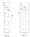
- FIGS. 10 & 11 illustrate plan views of exemplary die carriers that employ MEMS features for the registration of die
- FIGS. 12-14 illustrate exemplary embodiments of multi-level die carriers
- FIG. 15 illustrates an exemplary placement of an elastomeric material between a die carrier and die sub-carriers
- FIGS. 16A & 17 illustrate an exemplary pick-and-place system
- FIG. 16B illustrates an electrical contactor that may be registered with a die carrier similarly to how the pick-and-place head shown in FIG. 16A is registered with a die carrier;
- FIG. 18 illustrates an alternate configuration of registration features for a pick-and-place head or electrical contactor (as compared to what is shown in FIGS. 16A , 16 B & 17 );
- FIGS. 19A , 19 B, 19 C & 20 illustrate alternate ways to register a pick-and-place head or electrical contactor with a die carrier
- FIG. 21 illustrates the use of a capacitive probe to locate the edges of a singulated die
- FIG. 22 illustrates an exemplary optical precising bridge
- FIG. 23 illustrates a die carrier that employs a vacuum to adhere die to the die carrier
- FIG. 24 illustrates a die sub-carrier that, in combination with a die carrier such as the die carrier shown in FIG. 23 , employs a vacuum to adhere a die;
- FIG. 25 illustrates exemplary vertical contact pins
- FIG. 26 illustrates exemplary buckling beam pins
- FIG. 27 illustrates exemplary cantilever needles
- FIG. 28 illustrates exemplary bumps on a flex circuit
- FIG. 29 illustrates exemplary conductive elastomer bumps
- FIG. 30 illustrates exemplary MEMS spring pins
- FIG. 31 illustrates a first exemplary array of electrical contactors
- FIG. 32 illustrates a second exemplary array of electrical contactors
- FIG. 33 illustrates an exemplary method for assembling an array of electrical contactors on a substrate
- FIG. 34 illustrates an elastomeric interposer placed between an array of electrical contactors and a base substrate
- FIG. 35 illustrates the use of cameras to align the die carrier and array of electrical contactors shown in FIGS. 2 & 3 ;
- FIG. 36 illustrates an exemplary way to align and mate a die carrier and array of electrical contactors
- FIG. 37 illustrates a column of die sub-carriers passing through a precising bridge
- FIG. 38 illustrates pairs of kinematic alignment features
- FIG. 39 illustrates a kinematic alignment feature atop a spring assembly.
- a “singulated semiconductor die” is a semiconductor die that has been sawed, cut or otherwise separated from the semiconductor wafer on which it was formed.
- the semiconductor wafer material on which a semiconductor die is formed may be thinned. Thinning typically occurs before semiconductor die are separated from their wafer, though thinning could alternately be done after separation. Regardless, the phrase “singulated semiconductor die” is intended to cover both thinned and non-thinned semiconductor die. Singulated semiconductor die are sometimes referred to herein as “singulated die” or simply “die”.
- the temperature at which semiconductor die may be tested is limited to a range of about 80-90° C.
- SDT allows one to test singulated die at their maximum operating temperatures, enabling the identification of die that only fail at extreme temperatures, and again mitigating the likelihood that a stack of die or package will need to be discarded.
- the die When stacking die, the die are typically “thinned” (i.e., ground on their back side) to a smaller thickness before being assembled into a stack. Because thinning a semiconductor wafer makes the wafer non-planar and incompatible with traditional whole wafer testing methods, wafers are thinned after wafer testing is complete. However, the act of thinning a wafer can cause additional defects in semiconductor devices. SDT enables the test of singulated die after they have been thinned, thereby enabling the identification of die that have been damaged as a result of wafer thinning.
- probe cards are only able to test a subset of the die on a wafer, and the function of a wafer prober is to step (move) an untested part of the wafer into position under a probe head.
- the probe card technology for some types of semiconductors has advanced to a point that the probe head may contain enough probes to contact all of the die on a wafer at once.
- SDT changes this and removes a large impediment to greater parallelism in test.
- FIG. 1 illustrates an exemplary method 100 for testing a plurality of singulated die.
- the method 100 comprises 1) placing each of the singulated die on a surface of a die carrier (at block 102 ), 2) mating an array of electrical contactors with the plurality of singulated die (at block 104 ), and then 3) performing electrical tests on the plurality of singulated die, via the array of electrical contactors (at block 106 ).
- the electrical tests are performed on all of the singulated die in parallel.
- an “array of electrical contactors” is intended to cover any sort of interface that can be used to contact (or probe) the electrical contacts (e.g., bond pads) of a plurality of singulated die.
- FIG. 2 illustrates an exemplary die carrier 200 for use with the method 100 (or other methods).
- the die carrier 200 comprises at least first and second opposed surfaces 202 , 204 , such as a top surface 202 and a bottom surface 204 .
- One of the surfaces has a plurality of cavities (e.g., milled or other types of cavities 206 , 208 , 210 , 212 ) formed therein, with each of the cavities 206 , 208 , 210 , 212 having one or more cavity walls 214 , 216 , 218 , 220 .
- cavities e.g., milled or other types of cavities 206 , 208 , 210 , 212
- each cavity 206 , 208 , 210 , 212 is shown to have a rectangular shape and four cavity walls 214 , 216 , 218 , 220 .
- each cavity 206 , 208 , 210 , 212 may be sized just larger than the dimensions of a particular singulated die 222 , 224 , 226 , 228
- each cavity 206 , 208 , 210 , 212 preferably has x and y dimensions that are larger than the x and y dimensions of any singulated die that might be placed therein. This not only enables easier placement of a die 222 within a cavity 206 , but it also enables the die carrier 200 to be used with dies of different size.
- singulated die 222 , 224 , 226 , 228 are placed in some or all of the cavities 206 , 208 , 210 , 212 of the die carrier 200 . In some cases, and as discussed later in this description, it is not necessary to align (or at least precisely align) the die 222 , 224 , 226 , 228 within their cavities 206 , 208 , 210 , 212 .
- placing the singulated die 222 , 224 , 226 , 228 on the die carrier 200 may further comprise registering each of the singulated die 222 with one or more cavity walls 214 , 216 , such as cavity walls oriented in x and y dimensions.
- FIG. 2 illustrates a scenario where each singulated die 222 , 224 , 226 , 228 is positioned in its respective cavity 206 , 208 , 210 , 212 in the same way (e.g., registered to upper left cavity walls 214 , 216 when looking at the figure).
- FIG. 2 illustrates a scenario where each singulated die 222 , 224 , 226 , 228 is positioned in its respective cavity 206 , 208 , 210 , 212 in the same way (e.g., registered to upper left cavity walls 214 , 216 when looking at the figure).
- FIG. 4 illustrates an alternative die carrier 400 , where four singulated die 402 , 404 , 406 , 408 are registered to adjacent cavity walls, such that the four singulated die 402 , 404 , 406 , 408 form a cluster of die.
- the die arrangement shown in FIG. 2 might be useful where uniformity is desired, or where it is desired to mate a separate electrical contactor with each semiconductor die 222 , 224 , 226 , 228 .
- the die arrangement shown in FIG. 4 might be useful where it is desired to reduce the size of a single electrical contactor that mates with a set of four die.
- An exemplary electrical contactor 500 for mating with the arrangement of die shown in FIG. 4 is shown in FIG. 5 .
- FIG. 6 illustrates yet another alternative die carrier 600 .
- the die carrier 600 provides a single cavity 602 , with the single cavity 602 being large enough that different singulated die 604 , 606 , 608 , 610 can be registered with the intersecting walls at each of the cavity's corners.
- each of the die carriers 200 , 400 , 600 shown in FIGS. 2 , 4 & 6 is shown to carry four singulated die (such as the die 222 , 224 , 226 , 228 shown in FIG. 2 ).
- the cavity arrangements of the various die carriers 200 , 400 , 600 can be replicated so that a single die carrier is capable of holding as many die as desired.
- a single die carrier could hold a 2 ⁇ 2 array of die, a 3 ⁇ 3 array of die, a 250 ⁇ 500 array of die, or any other sized array of die.
- each of FIGS. 2 , 4 & 6 illustrates a die carrier 200 , 400 , 600 with rectangular die-holding cavities.
- the cavities need not be rectangular and could alternately be circular or have other shapes.
- the cavities could also be formed of intersecting shapes, such as 1) rectangles intersected by small circles at the corners thereof, or 2) intersecting circles.
- FIGS. 7-9 illustrate elevations of different cavity wall profiles 700 , 800 , 900 / 902 .
- FIG. 7 illustrates a vertical cavity wall 700 .
- FIG. 8 illustrates a sloped cavity wall 800 .
- FIG. 9 illustrates a vertical cavity wall 900 bounded by a bevel (or slope 902 ).
- the cavity walls 800 , 900 / 902 shown in FIGS. 8 & 9 help to correct any misplacement of a singulated die 802 , 904 dropped in a cavity 804 , 906 , while the cavity walls 700 , 900 / 902 shown in FIGS. 7 & 9 provide a better-defined wall for registering a die 702 , 904 .
- Other cavity wall profiles are also possible.
- Singulated die may be placed on a die carrier using a pick-and-place system, such as a system that picks up die using a vacuum, positions the die over their desired locations, and then places the die in their desired locations. If the pick-and-place system is “accurate enough”, no further movement of the die may be necessary. However, in those cases where the pick-and-place system is not “accurate enough”, the registration of a die with a cavity wall may need to be accomplished by moving the die. In some cases, moving a die on a die carrier may include using at least one of: a mechanical push, a vacuum pull, micro-fluidics, a positive pressure push, gravity, or vibration.
- a pick-and-place system such as a system that picks up die using a vacuum
- FIGS. 10 & 11 illustrate plan views of exemplary die carriers 1000 , 1100 that employ MEMS features 1002 , 1004 , 1102 , 1104 , 1106 for the registration of die 1006 , 1108 .
- the die carrier 1000 shown in FIG. 10 has a plurality of MEMS walls 1002 , 1004 formed thereon.
- the walls 1002 , 1004 are paired to provide L-shaped registration mechanisms, against which die 1006 may be registered.
- the MEMS features could comprise posts 1102 , 1104 , 1106 ( FIG. 11 ) or other MEMS features.
- placing 102 of the method 100 ( FIG.
- semiconductor die 1006 , 1108 may be registered with the MEMS features 1002 , 1004 , 1102 , 1104 , 1106 .
- Die that need to be moved on the surface of one of the die carriers 1000 , 1100 e.g. for registration purposes, can be moved similarly to how dies are moved within a die carrier cavity 206 ( FIG. 2 ).
- FIGS. 12-14 illustrate exemplary embodiments of multi-level die carriers 1200 , 1300 , 1400 , where singulated die 1202 , 1204 , 1206 are placed on a surface 1208 , 1302 or 1402 of a die carrier 1210 , 1304 or 1404 by 1) placing one ( FIG. 12 ) or more ( FIGS.
- a die carrier 1404 may be provided with a plurality of cavities 1406 , 1408 , 1410 , and the die sub-carriers 1306 , 1308 , 1310 may be registered to walls of the cavities 1406 , 1408 , 1410 (see FIG. 14 ).
- the die sub-carriers could be registered with MEMS features of a die carrier.
- the die sub-carriers 1212 , 1214 , 1216 , 1306 , 1308 , 1310 shown in FIGS. 12-14 may be formed similarly to the die carriers 200 , 400 , 600 , 1000 , 1100 shown in any of FIGS. 2 , 4 , 6 , 10 and 11 .
- an elastomeric material 1502 may be placed between a die carrier 1504 and its die sub-carriers 1506 , 1508 , 1510 .
- FIG. 15 illustrates a single sheet of elastomeric material 1502 placed between a die carrier 1504 and its die sub-carriers 1506 , 1508 , 1510 .
- separate elastomeric elements could be provided for each die sub-carrier 1506 , 1508 , 1510 , or separate elastomeric elements could be provided for different subsets of die sub-carriers.
- An advantage of providing an elastomeric material 1502 between a die carrier 1504 and its die sub-carriers 1506 , 1508 , 1510 is that it enables each die sub-carrier 1506 , 1508 , 1510 to move slightly in x, y, z and theta dimensions. This can be useful when registering a pick-and-place head or electrical contactor with the die sub-carriers 1506 , 1508 , 1510 , as will be discussed in greater detail later in this description.
- a spring or springs could also be used to provide freedom of movement between a die carrier 1504 and its die sub-carriers 1506 , 1508 , 1510 .
- multi-level die carriers 1200 , 1300 , 1400 , 1500 shown in FIGS. 12-15 are associated with one level of die sub-carriers, any number of die sub-carrier levels, holding any number of singulated die or other die sub-carriers, could be employed.
- Singulated die may be placed on die sub-carriers before or after the die sub-carriers are placed on a die carrier.
- an automated pick-and-place system may be used to place semiconductor die on a die carrier (or die sub-carrier).
- One exemplary pick-and-place system 1600 is shown in FIGS. 16A & 17 .
- the system 1600 is shown to have only one pick-and-place head 1602 , the system could alternately have multiple pick-and-place heads, or one pick-and-place head could be configured to pick multiple singulated die.
- Each pick-and-place head 1602 may “pick” a die 1604 using, for example, a vacuum.
- the pick-and-place head 1602 When using a pick-and-place head 1602 to place singulated die 1604 on a die carrier or die sub-carrier 1606 , the pick-and-place head 1602 may be provided with freedom of movement in the x, y, z and/or theta dimensions. Also, or alternately, a die sub-carrier 1606 may be provided with freedom of movement in the x, y, z and/or theta ( ⁇ ) dimension (see, e.g., FIG. 16A ).
- this freedom of movement coupled with registration features 1608 , 1610 , 1612 on the pick-and-place head 1602 and die carrier (or die sub-carrier 1606 ) can help to register a pick-and-place head 1602 with a die carrier (or die sub-carrier 1606 ), thereby correcting small alignment errors between the pick-and-place head 1602 and the die carrier (or die sub-carrier 1606 ).
- the registration feature 1608 of the pick-and-place head 1602 shown in FIGS. 16A & 17 is a wall.
- the wall is shown to surround a picked die 1604 , the wall could alternately be an L-shaped wall 1800 , as shown in FIG. 18 ; or, a pick-and-place head could be provided with other registration features (such as one or more blocks, pins, balls or horizontal cylinders).
- a registration feature may be, for example, machined into a pick-and-place head or formed on a pick-and-place head 1602 (e.g., via a MEMS fabrication process).
- the heads may be provided with individual or common registration features (or a mix of both—to grossly register all of the heads with a die carrier or die sub-carrier, and to individually register each head (or groups of heads) with particular singulated die or die sub-carriers).
- FIG. 16A illustrates an exemplary registration of a pick-and-place head 1602 with a die carrier cavity 1614 .
- the cavity walls 1616 , 1618 of the die carrier cavity 1614 may have a feature such as a shelf (or shelf and sub-wall 1610 , 1612 ) machined therein.
- the cavity walls 1616 , 1618 above the machined feature 1610 , 1612 may be sloped to guide the pick-and-place head 1602 into a defined position before a die 1604 is placed in the cavity 1614 , with the shelf 1610 , 1612 providing a z-stop for the pick-and-place head 1602 .
- the cavity walls 1616 , 1618 below the machined feature 1610 , 1612 may also be sloped, to guide a die as it is dropped from (or placed by) the pick-and-place head 1602 .
- an electrical contactor 302 e.g., a device for probing the die 1604
- an electrical contactor 302 may be provided with freedom of movement and/or a registration feature or features similar to those provided for the pick-and-place head 1602 . See, FIG. 16B .
- an electrical contactor 302 (or group of electrical contactors) may be registered with the cavity 1614 similarly to how a pick-and-place head 1602 may be registered with the cavity 1614 .
- FIGS. 19A & 19B illustrate an alternate way to register a pick-and-place head 1900 with a die carrier or die sub-carrier 1902 . That is, the die carrier 1902 shown in FIGS. 19A & 19B has one or more MEMS features (e.g., walls or posts 1904 , 1906 , 1908 ) formed thereon, and the pick-and-place head 1900 is moved using servo motors, stepper motors, piezoelectric actuators, air cylinders or other systems, until the walls 1910 of the pick-and-place head 1900 are registered with the MEMS feature(s) 1904 , 1906 , 1908 .
- MEMS features e.g., walls or posts 1904 , 1906 , 1908
- a z-stop for the pick-and-place head 1900 may be provided by the surface 1912 of the die carrier 1902 .
- An electrical contactor 1914 may be registered with a die carrier or sub-carrier 1902 in a similar fashion, as shown in FIG. 19C .
- FIG. 20 illustrates yet another way to register a pick-and-place head 2000 with a die carrier or die sub-carrier 2002 .
- either the pick-and-place head 2000 or the die sub-carrier 2002 may be provided with one or more balls 2004 , 2006 , 2008 (as shown), horizontal cylinders or other features that is/are designed to mate with corresponding V-grooves 2010 , 2012 , 2014 (as shown), concave cones or other features in or on the other one of the elements 2000 , 2002 .
- semiconductor die may be aligned by 1) using optical or capacitive methods to determine where die are, and 2) using a pick-and-place head, mechanical finger or other element to move, slide or rotate the die into their desired positions. For example, and as shown in FIG.
- a die carrier 1210 may be provided with one or more fiducials 1218 , 1220 , and an optically acquired image of the fiducial(s) 1218 , 1220 may be compared to a desired image of the fiducial(s) 1218 , 1220 to determine how a die 1202 should be placed or moved to achieve a proper alignment of the die 1202 on the die carrier 1210 .
- Fiducials 1218 , 1220 on a die carrier 1210 and die sub-carriers 1212 , 1214 , 1216 may also be used to align the die sub-carriers 1212 , 1214 , 1216 with the die carrier 1210 .
- fiducials 1218 , 1220 , 1222 , 1224 may take the form of markings, scribed lines, machined features or MEMS features on a die carrier 1210 (or die sub-carrier 1212 ).
- a capacitive probe 2100 could also be positioned or moved over a singulated die 2102 , and a capacitive edge sense method may be used to determine where the die 2102 has been placed (e.g., by sensing various capacitances, such as C 1 and C 2 . This information can then be compared to a desired die position to determine how or whether the die 2102 needs to be moved, slid or rotated into its desired position.
- capacitive edge sense methods have long been used to determine the correct placement of semiconductor wafers, for example, and these methods (or other methods) could be used to sense the edges of individual die.
- optical and/or capacitive methods can be used to simply determine “where” semiconductor die are on a carrier. That is, so long as the die are approximately where they should be, optical or capacitive methods can be used to construct a map of where the semiconductor die actually are.
- the map can variously include: locations of die edges, intersections of die edges, locations of die electrical contacts (e.g., bond pads) with respect to fiducials or edges on the die carrier (or on die sub-carriers), or other elements.
- the map can be used to appropriately position each of the electrical contactors in an array, so that each semiconductor die is contacted by a corresponding electrical contactor.
- semiconductor die need not be precisely registered or aligned with any particular feature, so long as their positions on a die carrier are approximately correct, and so long as their positions can be determined with sufficient resolution.
- FIG. 22 illustrates the use of an optical “precising bridge” 2200 to determine where die 2202 , 2204 , 2206 have been placed on a die carrier 2208 .
- the exemplary precising bridge 2200 is shown to have three optical detectors 2210 , 2212 , 2214 , each of which images the die 2202 , 2204 , 2206 on a die carrier 2208 .
- the die 2202 , 2204 , 2206 may be imaged row-by-row as the die carrier 2208 is moved transverse to the precising bridge 2200 .
- Machine vision software can then be used to compare the different two-dimensional images acquired by the optical detectors 2210 , 2212 , 2214 , and in combination with 1) a known height of the detectors 2210 , 2212 , 2214 with respect to the surface 2216 of the die carrier 2208 , and 2) known positions of the fiducials 2218 , 2220 , construct a map of where the die 2202 , 2204 , 2206 are positioned on the die carrier 2208 .
- Various other optical mapping methods can also be employed, as would be understood by one of ordinary skill in the optical mapping or machine vision arts.
- the die carrying surface of a die carrier may simply be flat. This makes a die carrier much simpler to manufacture.
- a flat die carrier may be especially useful when die are simply aligned on the die carrier (and not registered with any sort of mechanical feature of a die carrier or die sub-carrier), or when the positions of die are simply mapped (without the undertaking of any sort of registration or alignment).
- a generally flat surface of a die carrier may in some cases comprise vacuum holes or other features for the purpose of adhering die to its surface.
- the method 100 may further comprise a step of “adhering” each singulated die or die sub-carrier to the surface of the die carrier.
- die 2302 , 2304 , 2306 , 2308 may be adhered to the surface of a die carrier 2300 (and similarly, to the surfaces of die sub-carriers) by providing the carrier(s) 2300 with holes 2302 , 2304 or other features for pulling a vacuum through the carrier(s) 2300 .
- a positive pressure hold system may be used to force die against a die carrier.
- a tacky substance on the surface of a die carrier, or MEMS latches, may also be used to adhere die to a die carrier.
- a vacuum may be pulled through a die carrier 1210 by attaching a vacuum system to a vacuum port 1226 of the die carrier 1210 .
- the vacuum may be maintained via continued operation of the vacuum system.
- the vacuum may be maintained by means of a check valve or similar device (not shown).
- each die sub-carrier 1212 , 1214 , 1216 may be provided with its own vacuum port.
- die sub-carriers 1212 may be provided with holes 2402 on their die carrying surfaces 2404 and holes 2406 on surfaces 2408 opposite their die carrying surfaces 2404 .
- the die sub-carriers 1212 , 1214 , 1216 When the die sub-carriers 1212 , 1214 , 1216 are placed on a die carrier 1210 , a single vacuum may be pulled through the die carrier 1210 and die sub-carriers 1212 , 1214 , 1216 .
- the holes on the surface of the die carrier 1210 , or the holes on the bottom surfaces of the die sub-carriers 1212 , 1214 , 1216 may be sized larger than the holes on, for example, the surfaces of the die sub-carriers 1212 , 1214 , 1216 on which singulated die 1202 , 1204 , 1206 are placed. This can mitigate the need to closely align corresponding holes on the die carrier 1210 and die sub-carriers 1212 , 1214 , 1216 .
- the die sub-carriers 1212 , 1214 , 1216 can also be adhered to the surface 1208 of a die carrier 1210 using glue.
- glue For example, an ultraviolet curable epoxy may be applied to the surface 1208 of a die carrier 1210 (or to the undersides of die sub-carriers 1212 , 1214 , 1216 ) and then altered (e.g., cured) to adhere or release the die sub-carriers 1212 , 1214 , 1216 from the die carrier 1210 .
- a tacky substance on the surface of a die carrier, or MEMS latches, may also be used to adhere die sub-carriers to a die carrier.
- the elastomeric material 1502 may comprise holes for enabling a single vacuum to be pulled through the die carrier 1504 and die sub-carriers 1506 , 1508 , 1510 .
- the temperature of a die carrier and its die may need to be increased (e.g., to 90° C.) or decreased (e.g., to ⁇ 45° C.) prior to testing the die that have been placed on the die carrier.
- the die carrier and die may be heated before or after placement of the die.
- the die carrier and die may be heated prior to final registration, alignment or mapping of the die on the die carrier. In this manner, any thermal expansion of the die carrier or die can be factored into the registration, alignment or mapping of the die.
- One way to heat a die carrier, and thereby heat a plurality of singulated die, is via a thermal soaking operation.
- the effects of thermal expansion of die and die carriers can be compensated for by matching or compensating for the coefficients of thermal expansion (CTE) of the involved elements.
- CTE coefficients of thermal expansion
- the die carrier or die sub-carriers could be formed of a material with a similar CTE, such as ceramic, kovar or invar. If a die carrier is made of another material, and the CTE mismatch between the die carrier and its die is large, one way to bridge the CTE mismatch is to employ die sub-carriers formed of a material having an intermediate CTE.
- an electrical contactor is a device that provides an electrical interface to one singulated die.
- an electrical contactor may comprise a substrate with a plurality of electrical contacts extending therefrom.
- the substrate may take various forms, including those of: a printed circuit board (PCB), a high-temperature cofired ceramic (HTCC) substrate, or a low-temperature cofired ceramic (LTCC) substrate.
- the electrical contacts may also take various forms, including those of: vertical contact pins 2502 , 2504 , 2506 mounted to a substrate 2500 ( FIG. 25 ); buckling beam pins 2602 , 2604 , 2606 mounted to a substrate 2600 ( FIG.
- the electrical contacts may comprise MEMS contact elements that are co-fabricated on a substrate in parallel. In other cases, MEMS contact elements may be individually coupled to a substrate. Still alternately, the electrical contacts may comprise field-coupled transmitters/receivers (e.g., AC-coupled transmitters/receivers) that make “electrical contact” without making “mechanical contact”.
- an array of electrical contactors may be formed similarly to any of a wide range of conventional probe cards. However, because of the singulation of the die, the electrical contactors need not be laid out in a pattern that matches the formation of die on a wafer. Also, the number of electrical contactors can far exceed the number of die that are formed on a wafer.
- FIG. 31 illustrates one exemplary array 3100 of electrical contactors 3102 , 3104 , wherein the contactors 3102 , 3104 are arranged in a rectangular grid, and wherein the contactor grid is not confined to a generally circular periphery (such as the periphery of a wafer).
- an array of electrical contactors may be formed of individual or groups of electrical contactors, which individual or groups of electrical contactors can be independently replaced and/or maneuvered.
- individual or groups of electrical contactors are independently replaceable, the failure of one electrical contactor (or one group of electrical contactors) does not result in a need to discard the entire array.
- individual or groups of electrical contactors are independently maneuverable, better registration and electrical continuity can be achieved between the electrical contactors (or groups of electrical contactors) and their respective die.
- each electrical contactor 3200 may be coupled to its own set of servo motors, stepper motors or piezoelectric actuators 3202 , so that the electrical contactor 3200 can be moved to a desired position.
- the position of an electrical contactor 3200 may be controlled by optically acquiring an image of the electrical contactor 3200 (e.g., via a camera 3204 ), comparing the acquired image to an expected image, and then using differences in the acquired and expected images to determine how or whether the electrical contactor 3200 should be moved.
- a plurality of electrical contactors may be assembled onto a common substrate in much the same way as a plurality of singulated die are assembled (or placed) on a die carrier, but with a need to provide electrical connections through the common substrate.
- electrical contactors may in some cases be adhered to substrates using more permanent methods than those that are used to adhere die to a die carrier (e.g., via glues or epoxies, such as a UV-curable epoxy, vs. a vacuum).
- FIG. 33 illustrates one exemplary method 3300 for assembling an array of electrical contactors on a substrate.
- the steps of the method 3300 may be performed in orders other than the order shown.
- the method 3300 comprises forming the electrical contacts for a plurality of electrical contactors on a single substrate (at block 3302 ).
- the substrate has one or more layers of material upon which (or through) metallic traces are routed.
- the metallic traces connect to ones of the electrical contacts, and in some cases provide electrical paths to the back of the substrate.
- the substrate may be diced to form individual or N ⁇ M groups of electrical contactors (at block 3304 ).
- the edges of the electrical contactors may be used as registration features (similar to the walls of the electrical contactor shown in FIG. 16B and pick-and-place head shown in FIGS. 16 A and 17 ).
- the diced individual or groups of electrical contactors are then attached to a common base substrate (at block 3304 ). See, e.g., FIG. 3 , where a plurality of contactors 302 , 304 , 306 , 308 are attached to the substrate 300 .
- the base substrate is formed of a material that has a CTE that is the same (or similar to) that of the die that are being contacted. In the case of silicon die, the material of the base substrate might be ceramic, kovar or invar.
- the electrical contactors may be attached to the base substrate using a glue or epoxy, such as an ultraviolet curable epoxy.
- the base substrate 300 may be provided with two or more fiducials 310 , 312 ( FIG. 3 ) for aligning the electrical contactors 302 , 304 , 306 , 308 on the base substrate 300 using an optical alignment process (i.e., machine vision).
- the base substrate may comprise one or more layers of material upon which (or through) metallic traces are routed.
- the metallic traces connect to corresponding traces on the substrates of the electrical contactors and serve to provide electrical connections between a test system, such as automated test equipment (ATE), and the base substrate.
- the base substrate 300 may also be (or comprise) a printed circuit board (PCB), or other form of substrate, having traces or routes that carry signals to and from the electrical contactors 302 , 304 , 306 , 308 .
- PCB printed circuit board
- an elastomeric interposer ( 3400 ) may be placed between the electrical contactors 302 , 304 , 306 , 308 and the base substrate 300 . See, FIG. 34 . Alternately, separate elastomeric interposers could be provided for each electrical contactor (or for each electrical contactor group).
- An exemplary cross-section of an elastomeric interposer is shown in FIG. 29 and comprises a frame or substrate 2900 that holds a plurality of conductive elastomer bumps 2902 , 2904 , 2906 .
- An advantage of using an elastomeric interposer 3400 is that it enables each electrical contactor 302 , 304 , 306 , 308 or contactor group to move slightly in x, y, z and theta dimensions. This can be useful when registering the electrical contactors 302 , 304 , 306 , 308 with a plurality of singulated die.
- a spring or springs could also be used to provide freedom of movement between electrical contactors and a base substrate.
- a mechanical z-stop such as a number of walls or posts, may be co-fabricated with the electrical contacts (e.g., via a MEMS fabrication process).
- Mechanical registration features or fiducials may also be co-fabricated with the electrical contacts. The registration features may take various forms, such as those shown in FIGS. 16-20 and discussed previously with respect to a pick-and-place head.
- FIGS. 2 & 3 illustrate an exemplary die carrier 200 and array of electrical contactors 302 , 304 , 306 , 308 , each of which are provided with fiducials 230 , 232 , 310 , 312 .
- the die carrier 200 and electrical contactors 302 , 304 are aligned with one another by 1) using one or more cameras 3500 , 3502 to acquire images 3504 of the fiducials 230 , 232 , 310 , 312 , and 2) comparing the acquired images 3504 to desired images 3506 to determine how or whether one or both of the die carrier 200 and the electrical contactor array 302 , 304 should be moved in x, y and theta dimensions.
- Movements in x, y and theta dimensions may be achieved via motors, piezoelectric actuators, air cylinders or other mechanisms.
- one or both of the die carrier 200 and electrical contactor array 302 , 304 may be moved in a z-dimension (i.e., toward the other element) to mate the array of electrical contactors 302 , 304 with a plurality of singulated die 226 , 228 .
- Mechanical z-stops such as pins or walls may be provided on the die carrier 200 or contactor array, to provide the right amount of compression of the electrical contacts 3508 , 3510 on the electrical contactors 302 , 304 (and prevent over-compression).
- the die carrier 200 or electrical contactor array 302 , 304 may be actuated in the opposite z-direction, and the singulated die 226 , 228 on the die carrier 200 may be unloaded and sorted (based, for example, on whether die 226 , 228 are determined to be good, bad, or good within certain limits).
- FIG. 36 illustrates another exemplary way to align and mate a die carrier 3600 and array of electrical contactors 3602 .
- the carrier 3600 (or alternately the contactor array 3602 ) may be provided with a pair of alignment pins 3604 , 3606
- the contactor array 3602 (or carrier 3600 ) may be provided with a pair of precision located and drilled alignment holes 3608 , 3610 (or routed depressions).
- the two elements 3600 , 3602 are grossly aligned prior to moving the two elements 3600 , 3602 toward one another in a z-direction.
- the alignment pins 3604 , 3606 make contact with the alignment holes 3608 , 3610 , one or both of the die carrier 3600 and electrical contactor array 3602 are urged into alignment with the other.
- the depth of the holes 3608 , 3610 or length of the pins 3604 , 3606 may be used as z-stops.
- FIGS. 16B & 17 yet another way to align and mate a die carrier 1606 and array of electrical contactors is illustrated. That is, the same sort of wall 1608 that is formed on a pick-and-place head 1602 (e.g., an electro formed wall) may be formed on an electrical contactor 302 . In some cases, the wall 1608 may be co-fabricated with the electrical contacts 1622 of a contactor 302 , using the same fabrication process.
- a pick-and-place head 1602 e.g., an electro formed wall
- the wall 1608 may be co-fabricated with the electrical contacts 1622 of a contactor 302 , using the same fabrication process.
- the contactor 302 is provided with some amount of freedom of movement in the x, y and theta dimensions, the wall's contact with the wall or shelf 1610 , 1612 of the die cavity 1614 causes the contactor 302 to move as necessary so that it properly aligns with a die 1604 .
- an electrical contactor may be diced from a substrate with a high degree of precision (e.g., by means of a laser cutting process). The wall of the electrical contactor may then be used for registration with a die cavity 1604 , similarly to how an electro formed wall would be used.
- the MEMS features e.g., walls or posts 1904 , 1906 , 1908
- the MEMS features may comprise three posts 1904 , 1906 , 1908 .
- the electrical contactor 1914 By moving an electrical contactor 1914 close to the surface of the die carrier 1902 , and then moving the contactor 1914 in x, y and/or theta dimensions, the electrical contactor 1914 can be registered with the MEMS features 1904 , 1906 , 1908 . Once registered, the electrical contactor 1914 can be further moved in the z dimension until it bottoms out on the surface 1912 of the die carrier 1902 . All movements of the electrical contactor 1914 may be accomplished using servo motors, stepper motors, piezoelectric actuators, air cylinders or other systems. To ensure proper mating of the electrical contactor 1914 with a die 1604 , the surface 1912 of the die carrier 1902 should be precisely machined (i.e., flat).
- Another way to align and mate a die carrier and array of electrical contactors is to align or map a plurality of singulated die on a die carrier, and then use the known or mapped alignment to move electrical contactors into precise positions, prior to mating the electrical contactors with the die on the die carrier.
- Still another way to align and mate a die carrier and array of electrical contactors is to align singulated die with fiducials on individual die sub-carriers. Then, in response to a map of electrical contactor positions, fiducials on a die carrier and the die sub-carriers may be used to align each of the die sub-carriers with a corresponding electrical contactor. Each die sub-carrier may be moved in x, y and theta dimensions. As shown in FIG. 37 , one or more columns of die sub-carriers 3700 , 3702 , 3704 may be aligned, in parallel, at a “precising bridge” 3706 .
- the precising bridge 3706 is shown to have a number of capacitive sensors 3708 , 3710 , though optical sensors could also be used.
- each die sub-carrier 3700 , 3702 , 3704 is shown to be mounted to the die carrier 3712 via one or more piezoelectric elements 3714 , 3716 , 3718 . In this manner, the die sub-carriers 3700 , 3702 , 3704 may be individually moved to optimum positions in x, y and theta dimensions. Alternately, other technologies may be used to move or nudge the die sub-carriers 3700 , 3702 , 3704 into desired positions.
- an array of electrical contactors may be mated with a plurality of singulated die by mating corresponding kinematic features on the die carrier and the array of electrical contactors.
- the arrangement shown in FIG. 20 may be employed, wherein 1) one or more V-grooves 2010 , 2012 , 2014 are machined or formed in/on an electrical contactor instead of a pick-and-place head 2000 , and 2) one or more balls 2004 , 2006 , 2008 are attached to a die carrier 2002 .
- the V-grooves may be formed using a MEMS process, such as a Silicon KOH etch process where a sloped wall is sputtered and plated, and silicon is then etched away to leave a metal geometry with sloped walls.
- a MEMS process such as a Silicon KOH etch process where a sloped wall is sputtered and plated, and silicon is then etched away to leave a metal geometry with sloped walls.
- FIG. 38 illustrates a set of balls 2004 , 2006 , 2008 attached to a die carrier 2002 and a set of concave conical features 3802 , 3804 , 3806 machined or formed in/on an electrical contactor 3800 . Still other pairs of corresponding kinematic features can be employed. In all cases, one or more degrees of freedom in electrical contactor or die carrier movement are required, so that corresponding kinematic features can pull the electrical contactor, die carrier or die sub-carrier into position.
- FIG. 39 illustrates a kinematic alignment feature (e.g., a V-groove 3900 ) atop a spring assembly 3902 , which alignment feature 3900 and spring assembly 3902 can be formed using a MEMS process.
- the spring assembly 3902 provides a sequence to the contactor/sub-carrier mating process, whereby 1) x, y and theta registration of the contactor-to-sub-carrier is first achieved as the ball 3904 is mated with the alignment feature 3900 , 2) z-compression occurs because of the spring assembly 3902 , and 3) a hard z-stop 3906 associated with the aforementioned spring assembly 3902 ensures that the electrical contacts of the contactor 3908 are not over-compressed as the contactor 3908 is mated with the die sub-carrier 3910 .
- any of the above contactor/carrier mating methods may be applied to the mating of 1) individual or grouped electrical contactors with 2) either a die carrier or die sub-carriers.
- any alignment steps taken (or apparatus used) to align a plurality of electrical contactors could likewise be taken to align a plurality of singulated die.
- multiple, tiered contactor/carrier alignment mechanisms may be employed, such as pairs of alignment pins and holes to grossly align an array of electrical contactors with a die carrier, and per contactor/die sub-carrier kinematic alignment mechanisms for fine alignment of individual contactors with their respective die.
Abstract
Description
Claims (18)
Priority Applications (1)
| Application Number | Priority Date | Filing Date | Title |
|---|---|---|---|
| US12/549,049 US8884639B2 (en) | 2008-08-27 | 2009-08-27 | Methods, apparatus and articles of manufacture for testing a plurality of singulated die |
Applications Claiming Priority (2)
| Application Number | Priority Date | Filing Date | Title |
|---|---|---|---|
| US19035708P | 2008-08-27 | 2008-08-27 | |
| US12/549,049 US8884639B2 (en) | 2008-08-27 | 2009-08-27 | Methods, apparatus and articles of manufacture for testing a plurality of singulated die |
Publications (2)
| Publication Number | Publication Date |
|---|---|
| US20100109699A1 US20100109699A1 (en) | 2010-05-06 |
| US8884639B2 true US8884639B2 (en) | 2014-11-11 |
Family
ID=41722261
Family Applications (1)
| Application Number | Title | Priority Date | Filing Date |
|---|---|---|---|
| US12/549,049 Active 2031-01-07 US8884639B2 (en) | 2008-08-27 | 2009-08-27 | Methods, apparatus and articles of manufacture for testing a plurality of singulated die |
Country Status (3)
| Country | Link |
|---|---|
| US (1) | US8884639B2 (en) |
| TW (1) | TW201027647A (en) |
| WO (1) | WO2010025231A2 (en) |
Cited By (3)
| Publication number | Priority date | Publication date | Assignee | Title |
|---|---|---|---|---|
| US20140062516A1 (en) * | 2011-03-21 | 2014-03-06 | University Of Windsor | Apparatus for the Automated Testing and Validation of Electronic Components |
| US20150123693A1 (en) * | 2013-11-07 | 2015-05-07 | Nidec-Read Corporation | Inspection jig |
| US10782315B2 (en) | 2017-04-17 | 2020-09-22 | Rosemount Aerospace Inc. | Apparatus and method for packaging, handling or testing of sensors |
Families Citing this family (6)
| Publication number | Priority date | Publication date | Assignee | Title |
|---|---|---|---|---|
| CN106970314A (en) * | 2013-11-11 | 2017-07-21 | 罗斯柯公司 | The method of component processing assembly and processing component |
| JP2016095272A (en) * | 2014-11-17 | 2016-05-26 | 三菱電機株式会社 | Semiconductor evaluation device, semiconductor evaluation method and test jig |
| US9658286B2 (en) | 2014-12-18 | 2017-05-23 | Freescale Semiconductor, Inc. | Sequential access assembly strip test adapter |
| TWI721147B (en) | 2016-04-04 | 2021-03-11 | 美商矽立科技有限公司 | Apparatus and methods for integrated mems devices |
| US10481197B2 (en) * | 2016-12-27 | 2019-11-19 | Nanning Fugui Precision Industrial Co., Ltd. | Circuit board testing device and chassis for same |
| US10368448B2 (en) | 2017-11-11 | 2019-07-30 | At&S Austria Technologie & Systemtechnik Aktiengesellschaft | Method of manufacturing a component carrier |
Citations (30)
| Publication number | Priority date | Publication date | Assignee | Title |
|---|---|---|---|---|
| US5279975A (en) | 1992-02-07 | 1994-01-18 | Micron Technology, Inc. | Method of testing individual dies on semiconductor wafers prior to singulation |
| US5475317A (en) * | 1993-12-23 | 1995-12-12 | Epi Technologies, Inc. | Singulated bare die tester and method of performing forced temperature electrical tests and burn-in |
| US5654204A (en) | 1994-07-20 | 1997-08-05 | Anderson; James C. | Die sorter |
| US5985682A (en) * | 1997-08-25 | 1999-11-16 | Motorola, Inc. | Method for testing a bumped semiconductor die |
| US6373268B1 (en) | 1999-05-10 | 2002-04-16 | Intel Corporation | Test handling method and equipment for conjoined integrated circuit dice |
| US6406246B1 (en) | 1998-12-15 | 2002-06-18 | Advantest Corporation | Device handler |
| US6583635B2 (en) * | 2001-03-15 | 2003-06-24 | Micron Technology, Inc. | Semiconductor die test carrier having conductive elastomeric interposer |
| US20030129775A1 (en) | 2000-07-31 | 2003-07-10 | Kline Jerry D. | Matched set of integrated circuit chips selected from a multi wafer interposer |
| US6627483B2 (en) * | 1998-12-04 | 2003-09-30 | Formfactor, Inc. | Method for mounting an electronic component |
| WO2004001428A1 (en) | 2002-06-19 | 2003-12-31 | Formfactor, Inc. | Test method for yielding a known good die |
| US6720786B2 (en) * | 2001-07-25 | 2004-04-13 | Integrated Device Technology, Inc. | Lead formation, assembly strip test, and singulation system |
| JP2004340696A (en) | 2003-05-15 | 2004-12-02 | Toyo Commun Equip Co Ltd | Measurement apparatus for chip electronic component |
| US6897670B2 (en) | 2001-12-21 | 2005-05-24 | Texas Instruments Incorporated | Parallel integrated circuit test apparatus and test method |
| US20050225344A1 (en) * | 2003-03-06 | 2005-10-13 | Kirby Kyle K | Interconnect having spring contacts |
| US7045035B1 (en) | 2004-04-08 | 2006-05-16 | National Semiconductor Corporation | Post singulation die separation apparatus and method for bulk feeding operation |
| US20060145338A1 (en) * | 2004-12-31 | 2006-07-06 | Wen-Chang Dong | Thin film with MEMS probe circuits and MEMS thin film probe head using the same |
| US20060290367A1 (en) * | 2005-06-24 | 2006-12-28 | Formfactor, Inc. | Method and apparatus for adjusting a multi-substrate probe structure |
| US20070007987A1 (en) * | 2005-02-14 | 2007-01-11 | Farnworth Warren M | System for testing semiconductor components |
| US20070063721A1 (en) | 2005-09-19 | 2007-03-22 | Formfactor, Inc. | Apparatus And Method Of Testing Singulated Dies |
| US20070216437A1 (en) * | 2006-03-14 | 2007-09-20 | Micron Technology, Inc. | Pusher assemblies for use in microfeature device testing, systems with pusher assemblies, and methods for using such pusher assemblies |
| US20080233663A1 (en) | 2007-03-20 | 2008-09-25 | Spansion Llc | Singulated bare die testing |
| US20080252330A1 (en) | 2007-04-16 | 2008-10-16 | Verigy Corporation | Method and apparatus for singulated die testing |
| US20090079452A1 (en) * | 2007-09-26 | 2009-03-26 | Formfactor, Inc. | Component assembly and alignment |
| US20100039133A1 (en) * | 2008-08-13 | 2010-02-18 | Formfactor, Inc. | Probe head controlling mechanism for probe card assemblies |
| US7699616B2 (en) * | 2001-06-20 | 2010-04-20 | Formfactor, Inc. | High density planar electrical interface |
| US7940070B2 (en) * | 2009-04-08 | 2011-05-10 | Nichepac Technology Inc. | Singulated bare die testing fixture |
| US8044673B1 (en) * | 2010-04-28 | 2011-10-25 | Lajos Burgyan | Method and apparatus for positioning and contacting singulated semiconductor dies |
| US8102184B2 (en) * | 2006-01-17 | 2012-01-24 | Johnstech International | Test contact system for testing integrated circuits with packages having an array of signal and power contacts |
| US8496113B2 (en) * | 2007-04-13 | 2013-07-30 | Techwing Co., Ltd. | Insert for carrier board of test handler |
| US8550443B1 (en) * | 2009-03-11 | 2013-10-08 | Centipede Systems, Inc. | Method and apparatus for holding microelectronic devices |
Family Cites Families (1)
| Publication number | Priority date | Publication date | Assignee | Title |
|---|---|---|---|---|
| US5897670A (en) * | 1996-07-12 | 1999-04-27 | Sun Microsystems, Inc. | Method and system for efficient organization of selectable elements on a graphical user interface |
-
2009
- 2009-08-27 US US12/549,049 patent/US8884639B2/en active Active
- 2009-08-27 WO PCT/US2009/055165 patent/WO2010025231A2/en active Application Filing
- 2009-08-27 TW TW98128806A patent/TW201027647A/en unknown
Patent Citations (34)
| Publication number | Priority date | Publication date | Assignee | Title |
|---|---|---|---|---|
| US5279975A (en) | 1992-02-07 | 1994-01-18 | Micron Technology, Inc. | Method of testing individual dies on semiconductor wafers prior to singulation |
| US5475317A (en) * | 1993-12-23 | 1995-12-12 | Epi Technologies, Inc. | Singulated bare die tester and method of performing forced temperature electrical tests and burn-in |
| US5654204A (en) | 1994-07-20 | 1997-08-05 | Anderson; James C. | Die sorter |
| US5985682A (en) * | 1997-08-25 | 1999-11-16 | Motorola, Inc. | Method for testing a bumped semiconductor die |
| US6627483B2 (en) * | 1998-12-04 | 2003-09-30 | Formfactor, Inc. | Method for mounting an electronic component |
| US20070269909A1 (en) * | 1998-12-04 | 2007-11-22 | Formfactor, Inc. | Method for processing an integrated circuit |
| US6406246B1 (en) | 1998-12-15 | 2002-06-18 | Advantest Corporation | Device handler |
| US6373268B1 (en) | 1999-05-10 | 2002-04-16 | Intel Corporation | Test handling method and equipment for conjoined integrated circuit dice |
| US20030129775A1 (en) | 2000-07-31 | 2003-07-10 | Kline Jerry D. | Matched set of integrated circuit chips selected from a multi wafer interposer |
| US6583635B2 (en) * | 2001-03-15 | 2003-06-24 | Micron Technology, Inc. | Semiconductor die test carrier having conductive elastomeric interposer |
| US7699616B2 (en) * | 2001-06-20 | 2010-04-20 | Formfactor, Inc. | High density planar electrical interface |
| US6720786B2 (en) * | 2001-07-25 | 2004-04-13 | Integrated Device Technology, Inc. | Lead formation, assembly strip test, and singulation system |
| US6897670B2 (en) | 2001-12-21 | 2005-05-24 | Texas Instruments Incorporated | Parallel integrated circuit test apparatus and test method |
| WO2004001428A1 (en) | 2002-06-19 | 2003-12-31 | Formfactor, Inc. | Test method for yielding a known good die |
| US20050225344A1 (en) * | 2003-03-06 | 2005-10-13 | Kirby Kyle K | Interconnect having spring contacts |
| JP2004340696A (en) | 2003-05-15 | 2004-12-02 | Toyo Commun Equip Co Ltd | Measurement apparatus for chip electronic component |
| US7045035B1 (en) | 2004-04-08 | 2006-05-16 | National Semiconductor Corporation | Post singulation die separation apparatus and method for bulk feeding operation |
| US20060145338A1 (en) * | 2004-12-31 | 2006-07-06 | Wen-Chang Dong | Thin film with MEMS probe circuits and MEMS thin film probe head using the same |
| US20070007987A1 (en) * | 2005-02-14 | 2007-01-11 | Farnworth Warren M | System for testing semiconductor components |
| US20060290367A1 (en) * | 2005-06-24 | 2006-12-28 | Formfactor, Inc. | Method and apparatus for adjusting a multi-substrate probe structure |
| WO2007035664A2 (en) | 2005-09-19 | 2007-03-29 | Formfactor, Inc. | Apparatus and method of testing singulated dies |
| US8513969B2 (en) * | 2005-09-19 | 2013-08-20 | Formfactor, Inc. | Apparatus and method of testing singulated dies |
| US20070063721A1 (en) | 2005-09-19 | 2007-03-22 | Formfactor, Inc. | Apparatus And Method Of Testing Singulated Dies |
| US20100244873A1 (en) * | 2005-09-19 | 2010-09-30 | Formfactor, Inc. | Apparatus and method of testing singulated dies |
| US8102184B2 (en) * | 2006-01-17 | 2012-01-24 | Johnstech International | Test contact system for testing integrated circuits with packages having an array of signal and power contacts |
| US20070216437A1 (en) * | 2006-03-14 | 2007-09-20 | Micron Technology, Inc. | Pusher assemblies for use in microfeature device testing, systems with pusher assemblies, and methods for using such pusher assemblies |
| US20080233663A1 (en) | 2007-03-20 | 2008-09-25 | Spansion Llc | Singulated bare die testing |
| US8496113B2 (en) * | 2007-04-13 | 2013-07-30 | Techwing Co., Ltd. | Insert for carrier board of test handler |
| US20080252330A1 (en) | 2007-04-16 | 2008-10-16 | Verigy Corporation | Method and apparatus for singulated die testing |
| US20090079452A1 (en) * | 2007-09-26 | 2009-03-26 | Formfactor, Inc. | Component assembly and alignment |
| US20100039133A1 (en) * | 2008-08-13 | 2010-02-18 | Formfactor, Inc. | Probe head controlling mechanism for probe card assemblies |
| US8550443B1 (en) * | 2009-03-11 | 2013-10-08 | Centipede Systems, Inc. | Method and apparatus for holding microelectronic devices |
| US7940070B2 (en) * | 2009-04-08 | 2011-05-10 | Nichepac Technology Inc. | Singulated bare die testing fixture |
| US8044673B1 (en) * | 2010-04-28 | 2011-10-25 | Lajos Burgyan | Method and apparatus for positioning and contacting singulated semiconductor dies |
Non-Patent Citations (1)
| Title |
|---|
| International Search Report and Written Opinion mailed Apr. 2, 2010 for application No. PCT/US2009/055165. |
Cited By (6)
| Publication number | Priority date | Publication date | Assignee | Title |
|---|---|---|---|---|
| US20140062516A1 (en) * | 2011-03-21 | 2014-03-06 | University Of Windsor | Apparatus for the Automated Testing and Validation of Electronic Components |
| US9261533B2 (en) * | 2011-03-21 | 2016-02-16 | University Of Windsor | Apparatus for the automated testing and validation of electronic components |
| US20150123693A1 (en) * | 2013-11-07 | 2015-05-07 | Nidec-Read Corporation | Inspection jig |
| US9733299B2 (en) * | 2013-11-07 | 2017-08-15 | Nidec-Read Corporation | Inspection jig |
| US10782315B2 (en) | 2017-04-17 | 2020-09-22 | Rosemount Aerospace Inc. | Apparatus and method for packaging, handling or testing of sensors |
| US10935569B2 (en) | 2017-04-17 | 2021-03-02 | Rosemount Aerospace Inc. | Apparatus and method for packaging, handling or testing of sensors |
Also Published As
| Publication number | Publication date |
|---|---|
| US20100109699A1 (en) | 2010-05-06 |
| WO2010025231A3 (en) | 2010-05-27 |
| TW201027647A (en) | 2010-07-16 |
| WO2010025231A2 (en) | 2010-03-04 |
Similar Documents
| Publication | Publication Date | Title |
|---|---|---|
| US8884639B2 (en) | Methods, apparatus and articles of manufacture for testing a plurality of singulated die | |
| CN101303371B (en) | Probe card and method for fabricating the same | |
| CN101919039B (en) | A method and device for aligning components | |
| US8957691B2 (en) | Probe cards for probing integrated circuits | |
| US8872532B2 (en) | Wafer test cassette system | |
| US9335347B2 (en) | Method and apparatus for massively parallel multi-wafer test | |
| JP2010122202A (en) | Substrate inspection fixture and substrate inspection device using the same | |
| US11346861B2 (en) | Contact accuracy assurance method, contact accuracy assurance mechanism, and inspection apparatus | |
| US20090278926A1 (en) | Calibration method of electronic device test apparatus | |
| US6924656B2 (en) | Method and apparatus for testing BGA-type semiconductor devices | |
| US20140167798A1 (en) | System for post-processsing of electronic components | |
| US20070128076A1 (en) | Electrical test apparatus | |
| KR20090029806A (en) | Sawing tile corners on probe card substrates | |
| US8148646B2 (en) | Process of positioning groups of contact structures | |
| KR102164020B1 (en) | Probe head manufacturing method of the probe card | |
| KR101284774B1 (en) | Probe card and manufacturing method thereof | |
| US20100126289A1 (en) | Method of mounting contactor | |
| JP3400340B2 (en) | Flip chip bonding method and apparatus | |
| US20120194209A1 (en) | System and method for picking and placement of chip dies | |
| KR100982343B1 (en) | Apparatus for measuring and calibrating error of stage in wafer prober | |
| US10935570B2 (en) | Intermediate connection member and inspection apparatus | |
| US11525859B2 (en) | Insertion/extraction mechanism and method for replacing block member | |
| KR101062368B1 (en) | Probe Card and Wafer Test Method Using the Same | |
| JPH01213181A (en) | Tray to contain semiconductor element |
Legal Events
| Date | Code | Title | Description |
|---|---|---|---|
| AS | Assignment |
Owner name: ADVANTEST (SINGAPORE) PTE LTD, SINGAPORE Free format text: ASSIGNMENT OF ASSIGNORS INTEREST;ASSIGNOR:VERIGY (SINGAPORE) PTE LTD;REEL/FRAME:027896/0018 Effective date: 20120302 |
|
| STCF | Information on status: patent grant |
Free format text: PATENTED CASE |
|
| AS | Assignment |
Owner name: ADVANTEST CORPORATION, JAPAN Free format text: ASSIGNMENT OF ASSIGNORS INTEREST;ASSIGNOR:ADVANTEST (SINGAPORE) PTE. LTD.;REEL/FRAME:035371/0265 Effective date: 20150401 |
|
| AS | Assignment |
Owner name: ADVANTEST CORPORATION, JAPAN Free format text: CORRECTIVE ASSIGNMENT TO CORRECT THE ASSIGNEE ADDRESS PREVIOUSLY RECORDED AT REEL: 035371 FRAME: 0265. ASSIGNOR(S) HEREBY CONFIRMS THE ASSIGNMENT;ASSIGNOR:ADVANTEST (SINGAPORE) PTE. LTD.;REEL/FRAME:035425/0768 Effective date: 20150401 |
|
| MAFP | Maintenance fee payment |
Free format text: PAYMENT OF MAINTENANCE FEE, 4TH YEAR, LARGE ENTITY (ORIGINAL EVENT CODE: M1551) Year of fee payment: 4 |
|
| AS | Assignment |
Owner name: ADVANTEST CORPORATION, JAPAN Free format text: CHANGE OF ADDRESS;ASSIGNOR:ADVANTEST CORPORATION;REEL/FRAME:047987/0626 Effective date: 20181112 |
|
| MAFP | Maintenance fee payment |
Free format text: PAYMENT OF MAINTENANCE FEE, 8TH YEAR, LARGE ENTITY (ORIGINAL EVENT CODE: M1552); ENTITY STATUS OF PATENT OWNER: LARGE ENTITY Year of fee payment: 8 |