US8872280B2 - Non-planar FET and manufacturing method thereof - Google Patents
Non-planar FET and manufacturing method thereof Download PDFInfo
- Publication number
- US8872280B2 US8872280B2 US13/562,322 US201213562322A US8872280B2 US 8872280 B2 US8872280 B2 US 8872280B2 US 201213562322 A US201213562322 A US 201213562322A US 8872280 B2 US8872280 B2 US 8872280B2
- Authority
- US
- United States
- Prior art keywords
- fin structure
- sub spacer
- substrate
- planar fet
- layer
- Prior art date
- Legal status (The legal status is an assumption and is not a legal conclusion. Google has not performed a legal analysis and makes no representation as to the accuracy of the status listed.)
- Active, expires
Links
- 238000004519 manufacturing process Methods 0.000 title description 7
- 238000002353 field-effect transistor method Methods 0.000 title 1
- 125000006850 spacer group Chemical group 0.000 claims abstract description 45
- 239000000758 substrate Substances 0.000 claims abstract description 32
- 238000005530 etching Methods 0.000 claims description 27
- 238000002955 isolation Methods 0.000 claims description 19
- 239000000463 material Substances 0.000 claims description 18
- 238000000034 method Methods 0.000 abstract description 39
- 239000010410 layer Substances 0.000 description 48
- 238000009413 insulation Methods 0.000 description 7
- 238000001312 dry etching Methods 0.000 description 6
- VYPSYNLAJGMNEJ-UHFFFAOYSA-N Silicium dioxide Chemical compound O=[Si]=O VYPSYNLAJGMNEJ-UHFFFAOYSA-N 0.000 description 5
- 229910052814 silicon oxide Inorganic materials 0.000 description 5
- 229910052581 Si3N4 Inorganic materials 0.000 description 4
- 238000000231 atomic layer deposition Methods 0.000 description 4
- 238000010586 diagram Methods 0.000 description 4
- HQVNEWCFYHHQES-UHFFFAOYSA-N silicon nitride Chemical compound N12[Si]34N5[Si]62N3[Si]51N64 HQVNEWCFYHHQES-UHFFFAOYSA-N 0.000 description 4
- XUIMIQQOPSSXEZ-UHFFFAOYSA-N Silicon Chemical compound [Si] XUIMIQQOPSSXEZ-UHFFFAOYSA-N 0.000 description 3
- 229910052710 silicon Inorganic materials 0.000 description 3
- 239000010703 silicon Substances 0.000 description 3
- 229910052454 barium strontium titanate Inorganic materials 0.000 description 2
- 238000007796 conventional method Methods 0.000 description 2
- 239000003989 dielectric material Substances 0.000 description 2
- 239000007943 implant Substances 0.000 description 2
- 239000011229 interlayer Substances 0.000 description 2
- 150000002500 ions Chemical class 0.000 description 2
- 229910052451 lead zirconate titanate Inorganic materials 0.000 description 2
- TWNQGVIAIRXVLR-UHFFFAOYSA-N oxo(oxoalumanyloxy)alumane Chemical compound O=[Al]O[Al]=O TWNQGVIAIRXVLR-UHFFFAOYSA-N 0.000 description 2
- SIWVEOZUMHYXCS-UHFFFAOYSA-N oxo(oxoyttriooxy)yttrium Chemical compound O=[Y]O[Y]=O SIWVEOZUMHYXCS-UHFFFAOYSA-N 0.000 description 2
- RVTZCBVAJQQJTK-UHFFFAOYSA-N oxygen(2-);zirconium(4+) Chemical compound [O-2].[O-2].[Zr+4] RVTZCBVAJQQJTK-UHFFFAOYSA-N 0.000 description 2
- 230000037361 pathway Effects 0.000 description 2
- HBMJWWWQQXIZIP-UHFFFAOYSA-N silicon carbide Chemical compound [Si+]#[C-] HBMJWWWQQXIZIP-UHFFFAOYSA-N 0.000 description 2
- 229910001928 zirconium oxide Inorganic materials 0.000 description 2
- 229910015846 BaxSr1-xTiO3 Inorganic materials 0.000 description 1
- 229910020696 PbZrxTi1−xO3 Inorganic materials 0.000 description 1
- 229910000577 Silicon-germanium Inorganic materials 0.000 description 1
- LEVVHYCKPQWKOP-UHFFFAOYSA-N [Si].[Ge] Chemical compound [Si].[Ge] LEVVHYCKPQWKOP-UHFFFAOYSA-N 0.000 description 1
- CEPICIBPGDWCRU-UHFFFAOYSA-N [Si].[Hf] Chemical compound [Si].[Hf] CEPICIBPGDWCRU-UHFFFAOYSA-N 0.000 description 1
- ILCYGSITMBHYNK-UHFFFAOYSA-N [Si]=O.[Hf] Chemical compound [Si]=O.[Hf] ILCYGSITMBHYNK-UHFFFAOYSA-N 0.000 description 1
- VNSWULZVUKFJHK-UHFFFAOYSA-N [Sr].[Bi] Chemical compound [Sr].[Bi] VNSWULZVUKFJHK-UHFFFAOYSA-N 0.000 description 1
- 230000004075 alteration Effects 0.000 description 1
- 239000004020 conductor Substances 0.000 description 1
- 230000005669 field effect Effects 0.000 description 1
- KQHQLIAOAVMAOW-UHFFFAOYSA-N hafnium(4+) oxygen(2-) zirconium(4+) Chemical compound [O--].[O--].[O--].[O--].[Zr+4].[Hf+4] KQHQLIAOAVMAOW-UHFFFAOYSA-N 0.000 description 1
- CJNBYAVZURUTKZ-UHFFFAOYSA-N hafnium(iv) oxide Chemical compound O=[Hf]=O CJNBYAVZURUTKZ-UHFFFAOYSA-N 0.000 description 1
- 230000010354 integration Effects 0.000 description 1
- MRELNEQAGSRDBK-UHFFFAOYSA-N lanthanum(3+);oxygen(2-) Chemical compound [O-2].[O-2].[O-2].[La+3].[La+3] MRELNEQAGSRDBK-UHFFFAOYSA-N 0.000 description 1
- HFGPZNIAWCZYJU-UHFFFAOYSA-N lead zirconate titanate Chemical compound [O-2].[O-2].[O-2].[O-2].[O-2].[Ti+4].[Zr+4].[Pb+2] HFGPZNIAWCZYJU-UHFFFAOYSA-N 0.000 description 1
- 229910052751 metal Inorganic materials 0.000 description 1
- 239000002184 metal Substances 0.000 description 1
- 238000012986 modification Methods 0.000 description 1
- 230000004048 modification Effects 0.000 description 1
- 230000003647 oxidation Effects 0.000 description 1
- 238000007254 oxidation reaction Methods 0.000 description 1
- BPUBBGLMJRNUCC-UHFFFAOYSA-N oxygen(2-);tantalum(5+) Chemical compound [O-2].[O-2].[O-2].[O-2].[O-2].[Ta+5].[Ta+5] BPUBBGLMJRNUCC-UHFFFAOYSA-N 0.000 description 1
- 238000000059 patterning Methods 0.000 description 1
- 229910021420 polycrystalline silicon Inorganic materials 0.000 description 1
- 239000004065 semiconductor Substances 0.000 description 1
- 229910010271 silicon carbide Inorganic materials 0.000 description 1
- VEALVRVVWBQVSL-UHFFFAOYSA-N strontium titanate Chemical compound [Sr+2].[O-][Ti]([O-])=O VEALVRVVWBQVSL-UHFFFAOYSA-N 0.000 description 1
- 238000001039 wet etching Methods 0.000 description 1
- GFQYVLUOOAAOGM-UHFFFAOYSA-N zirconium(iv) silicate Chemical compound [Zr+4].[O-][Si]([O-])([O-])[O-] GFQYVLUOOAAOGM-UHFFFAOYSA-N 0.000 description 1
Images


Classifications
-
- H—ELECTRICITY
- H01—ELECTRIC ELEMENTS
- H01L—SEMICONDUCTOR DEVICES NOT COVERED BY CLASS H10
- H01L29/00—Semiconductor devices adapted for rectifying, amplifying, oscillating or switching, or capacitors or resistors with at least one potential-jump barrier or surface barrier, e.g. PN junction depletion layer or carrier concentration layer; Details of semiconductor bodies or of electrodes thereof ; Multistep manufacturing processes therefor
- H01L29/66—Types of semiconductor device ; Multistep manufacturing processes therefor
- H01L29/66007—Multistep manufacturing processes
- H01L29/66075—Multistep manufacturing processes of devices having semiconductor bodies comprising group 14 or group 13/15 materials
- H01L29/66227—Multistep manufacturing processes of devices having semiconductor bodies comprising group 14 or group 13/15 materials the devices being controllable only by the electric current supplied or the electric potential applied, to an electrode which does not carry the current to be rectified, amplified or switched, e.g. three-terminal devices
- H01L29/66409—Unipolar field-effect transistors
- H01L29/66477—Unipolar field-effect transistors with an insulated gate, i.e. MISFET
- H01L29/66787—Unipolar field-effect transistors with an insulated gate, i.e. MISFET with a gate at the side of the channel
- H01L29/66795—Unipolar field-effect transistors with an insulated gate, i.e. MISFET with a gate at the side of the channel with a horizontal current flow in a vertical sidewall of a semiconductor body, e.g. FinFET, MuGFET
-
- H—ELECTRICITY
- H01—ELECTRIC ELEMENTS
- H01L—SEMICONDUCTOR DEVICES NOT COVERED BY CLASS H10
- H01L29/00—Semiconductor devices adapted for rectifying, amplifying, oscillating or switching, or capacitors or resistors with at least one potential-jump barrier or surface barrier, e.g. PN junction depletion layer or carrier concentration layer; Details of semiconductor bodies or of electrodes thereof ; Multistep manufacturing processes therefor
- H01L29/40—Electrodes ; Multistep manufacturing processes therefor
- H01L29/43—Electrodes ; Multistep manufacturing processes therefor characterised by the materials of which they are formed
- H01L29/49—Metal-insulator-semiconductor electrodes, e.g. gates of MOSFET
- H01L29/51—Insulating materials associated therewith
-
- H—ELECTRICITY
- H01—ELECTRIC ELEMENTS
- H01L—SEMICONDUCTOR DEVICES NOT COVERED BY CLASS H10
- H01L29/00—Semiconductor devices adapted for rectifying, amplifying, oscillating or switching, or capacitors or resistors with at least one potential-jump barrier or surface barrier, e.g. PN junction depletion layer or carrier concentration layer; Details of semiconductor bodies or of electrodes thereof ; Multistep manufacturing processes therefor
- H01L29/66—Types of semiconductor device ; Multistep manufacturing processes therefor
- H01L29/66007—Multistep manufacturing processes
- H01L29/66075—Multistep manufacturing processes of devices having semiconductor bodies comprising group 14 or group 13/15 materials
- H01L29/66227—Multistep manufacturing processes of devices having semiconductor bodies comprising group 14 or group 13/15 materials the devices being controllable only by the electric current supplied or the electric potential applied, to an electrode which does not carry the current to be rectified, amplified or switched, e.g. three-terminal devices
- H01L29/66409—Unipolar field-effect transistors
- H01L29/66477—Unipolar field-effect transistors with an insulated gate, i.e. MISFET
- H01L29/66787—Unipolar field-effect transistors with an insulated gate, i.e. MISFET with a gate at the side of the channel
- H01L29/66795—Unipolar field-effect transistors with an insulated gate, i.e. MISFET with a gate at the side of the channel with a horizontal current flow in a vertical sidewall of a semiconductor body, e.g. FinFET, MuGFET
- H01L29/66818—Unipolar field-effect transistors with an insulated gate, i.e. MISFET with a gate at the side of the channel with a horizontal current flow in a vertical sidewall of a semiconductor body, e.g. FinFET, MuGFET the channel being thinned after patterning, e.g. sacrificial oxidation on fin
-
- H—ELECTRICITY
- H01—ELECTRIC ELEMENTS
- H01L—SEMICONDUCTOR DEVICES NOT COVERED BY CLASS H10
- H01L29/00—Semiconductor devices adapted for rectifying, amplifying, oscillating or switching, or capacitors or resistors with at least one potential-jump barrier or surface barrier, e.g. PN junction depletion layer or carrier concentration layer; Details of semiconductor bodies or of electrodes thereof ; Multistep manufacturing processes therefor
- H01L29/66—Types of semiconductor device ; Multistep manufacturing processes therefor
- H01L29/68—Types of semiconductor device ; Multistep manufacturing processes therefor controllable by only the electric current supplied, or only the electric potential applied, to an electrode which does not carry the current to be rectified, amplified or switched
- H01L29/76—Unipolar devices, e.g. field effect transistors
- H01L29/772—Field effect transistors
- H01L29/78—Field effect transistors with field effect produced by an insulated gate
- H01L29/785—Field effect transistors with field effect produced by an insulated gate having a channel with a horizontal current flow in a vertical sidewall of a semiconductor body, e.g. FinFET, MuGFET
Definitions
- the present invention relates to a non-planar FET and a manufacturing method thereof, and more particularly to a non-planar FET which includes a sub spacer only on a middle sidewall of the fin structure and a manufacturing method thereof
- Non-planar transistors such as fin field effect transistors (Fin-FET) have been therefore introduced to reach a high drive current and to lower short channel effects.
- Fin-FET fin field effect transistors
- the height of the fin structure which corresponds to the channel width, is hard to control due to the use of HF in the etching process when patterning the substrate to form the fin structure. The quality of the Fin-FET is therefore affected.
- the present invention provides a non-planar FET and a manufacturing method thereof, in which the non-planar FET includes a sub spacer only on a middle sidewall of the fin structure.
- the non-planar FET in the present invention includes a substrate, a fin structure, a sub spacer, a gate, a dielectric layer and a source/drain region.
- the fin structure is disposed on the substrate.
- the sub spacer is disposed only on a middle sidewall of the fin structure.
- the gate is disposed on the fin structure.
- the dielectric layer is disposed between the fin structure and the gate.
- the source/drain region is disposed in the fin structure.
- a method of forming a non-planar FET is provided. First, a substrate is provided. A plurality of fin structures and a plurality of sub-spacer disposed only on a middle sidewall of the fin structure are formed on the substrate. Then, a gate is formed on the fin structure. Finally, a source/drain region is formed in the fin structure.
- the present invention provides a sub spacer that is formed only on the middle sidewall of the fin structure.
- the sub spacer is formed in the concave part of the fin structure.
- the sub spacer stretches outwardly from the fin structure and forms a wing-like structure.
- the position of the sub spacer in the present invention can be well controlled, so that the channel length of the non-planar FET in the present invention can also be well controlled, thereby improving the performance of the device.
- FIG. 1 to FIG. 10 are schematic diagrams of the method of manufacturing the non-planar FET of the present invention.
- FIG. 11 to FIG. 15 are schematic diagrams of the non-planar FET according to another embodiment in the present invention.
- FIG. 1 to FIG. 10 are schematic diagrams of the method of manufacturing the non-planar-FET in the present invention.
- a substrate 300 is provided.
- the substrate 300 may include a silicon substrate, an epitaxial silicon substrate, a silicon germanium substrate, or a silicon carbide substrate, but is not limited thereto.
- a plurality of active regions 400 and an isolation region 402 are defined on the substrate 300 .
- the active regions 400 are encompassed by the isolation regions 402 .
- at least a non-planar FET will be formed in the active region 400 while a shallow trench isolation (STI) is formed in the isolation region 402 .
- STI shallow trench isolation
- the present embodiment shows two active regions 400 that are encompassed by the isolation regions 402 . In another embodiment, only one active region 400 is encompassed by the isolation region 402 . In another embodiment, more than two active regions 400 are encompassed by the isolation regions 402 .
- An optional patterned liner layer 302 and a patterned mask layer 304 are formed on the substrate 300 .
- the patterned liner layer 302 and the patterned mask layer 304 are formed on the substrate 300 in the active regions 400 , but are not formed on the substrate 300 in the isolation region 402 .
- the patterned liner layer 302 may include SiO 2
- the patterned mask layer 304 may include SiN.
- the patterned mask layer 304 can include other materials suitable for a use in a hard mask, such as silicon carbide (SiC), silicon oxynitride (SiON) or a advanced pattern film (APF) provided by the Applied Material Corporation, or a combination thereof.
- SiC silicon carbide
- SiON silicon oxynitride
- API advanced pattern film
- a first etching process 307 is performed by using the patterned hard mask layer 304 as a mask to form a plurality of first trenches 303 in the isolation region 402 .
- the first trench 303 has a depth h 1 comprised between 200 angstroms to 300 angstroms, but is not limited thereto.
- the first etching process 307 is an anisotropic etching process, such as a dry etching process.
- a second etching process 309 is carried out to further remove the substrate 300 in the isolation region 402 and a part of the substrate 300 in the active region 400 to form a plurality of second trenches 305 .
- a concave portion 306 is therefore formed at the corner of the sidewall and the bottom surface of the second trench 305 . It is worth noting that the concave portion 306 is preferably located deeper than the depth h 1 .
- the second etching process 309 is an anisotropic etching process, such as a dry etching process using an etching recipe different form that of the first etching process 307 .
- FIG. 1 is another example, as shown in FIG.
- the second etching process 309 may be an isotropic etching process such as a wet etching process in which a spacer 308 is formed on the sidewall of the first trench 303 so that the concave structure 306 can be formed in the substrate 300 that is not covered by the spacer 308 .
- a third etching process 311 is performed to further remove the substrate 300 in the isolation region 402 so that the second trenches 305 become a plurality of third trenches 310 having a depth h 2 , which comprised between 2000 angstroms to 3000 angstroms.
- the third etching process 311 can, for example, be an anisotropic etching process, such as a dry etching process using the same recipe as the one in the first etching process 307 .
- a plurality of fin structures 312 is formed in the active region 400 , and each fin structure 312 has a concave portion 306 , thereby forming a “calabash-like” structure.
- the method of forming the calabash-like fin structure 312 is not limited to the etching steps described in FIG. 3 to FIG. 5 and can be formed by other methods.
- the calabash-like fin structure 312 can be formed by a plurality of etching steps and/or a laser process, but not limited thereto.
- a material layer 314 is formed on the substrate 300 .
- the material layer 314 is formed conformally along the third trenches 310 and filled into the concaves portions 306 .
- the material layer 314 is formed through an atomic layer deposition (ALD) process and the material layer 314 is silicon nitride (SiN).
- an etching process is carried out to remove the material layer 314 in the isolation regions 402 but the material layer 314 in the concave structures 306 is kept.
- the material layer 314 in the concave portions 306 becomes a sub spacer 315 .
- the etching process can, for example, be a dry etching process using the patterned mask layer 304 as a mask.
- a plurality of shallow trench isolations (STI) 316 is formed in the isolation region 402 .
- an insulation layer (not shown) can be formed on the substrate 300 to completely fill the third trenches 310 , and then an etching process is carried out to remove the insulation layer outside of the isolation regions 402 and a part of the insulation layer in the isolation regions 402 .
- the insulation layer is preferably removed until the sub spacer 315 is exposed. More preferably, the insulation layer is etched unit its top surface is lower than the sub spacer 315 .
- the material of the insulation layer i.e. the STI, has an etching selectivity with respect to the sub spacer 315 .
- the sub spacer 315 is preferably not etched.
- the STI 316 can include silicon oxide (SiO 2 ).
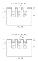
- FIG. 9 and FIG. 10 wherein FIG. 10 shows a three-dimensional view of the method in the present invention and FIG. 9 is a cross-sectional view taken along line A-A′.
- the patterned mask layer 304 and the patterned liner layer 302 are removed. In another embodiment, they can be maintained on the substrate 300 .
- a gate dielectric layer 318 is formed on the substrate 300 to cover the calabash-like fin structure 312 which preferably directly contacts the sub spacer 315 .
- the gate dielectric layer 318 includes SiO 2 which is evenly formed on the surface of the fin structure 312 through a thermal oxidation process.
- the gate dielectric layer 318 can include other materials such as a high-dielectric material which is formed through an atomic layer deposition (ALD) process.
- the high-dielectric material has a dielectric index substantially higher than 4 , like for example hafnium oxide (HfO 2 ), hafnium silicon oxide (HfSiO 4 ), hafnium silicon oxynitride (HfSiON), aluminum oxide (Al 2 O 3 ), lanthanum oxide (La 2 O 3 ), tantalum oxide (Ta 2 O 5 ), yttrium oxide (Y 2 O 3 ), zirconium oxide (ZrO 2 ), strontium titanate oxide (SrTiO 3 ), zirconium silicon oxide (ZrSiO 4 ), hafnium zirconium oxide (HfZrO 4 ), strontium bismuth tantalate (SrBi 2 Ta 2 O 9 , SBT), lead zirconate titanate (PbZr x Ti 1-
- a gate layer (not shown) is formed on the gate dielectric layer 318 .
- the gate layer may include various kinds of conductive material such as poly-silicon, metal or salicide.
- the gate layer is then patterned so that the gate layer becomes a required gate 320 structure.
- an ion implant process is performed to form a source region 322 a and a drain region 322 b in the fin structure 312 , as shown in FIG. 10 .
- a non-planar FET 324 is formed in the active region 400 .
- an inter-layer dielectric (ILD) layer (not shown) can be further formed on the non-planar FET 324 , and a plurality of contact holes (not shown) is formed therein to provide appropriate input/output pathway toward outer circuits.
- ILD inter-layer dielectric
- the non-planer FET 324 in the present embodiment includes a substrate 300 , a fin structure 312 , a sub spacer 315 , a gate 320 , a dielectric layer 318 , and a source/drain region 322 a and 322 b .
- the fin structure 312 has a calabash-like structure and has a concave portion 306 in the middle of the sidewall.
- the sub spacer 315 is filled into the concave portion 306 .
- the STI 316 is preferably lower than the sub spacer 315 .
- the fin height above the sub spacer 315 is comprised between 200 to 300 angstroms.
- FIG. 11 to FIG. 15 are schematic diagrams of the non-planar-FET according to another embodiment in the present invention.
- the former step is similar to that in the first embodiment shown in FIG. 1 , and the detailed description is omitted.
- FIG. 11 An etching process, such as a dry etching process, is carried out by using the patterned mask layer 304 as a mask to form the third trenches 310 in the isolation region.
- the third trench 310 has a depth H 2 which is comprised between 2000 angstroms to 3000 angstroms, but is not limited thereto.
- a plurality of fin structure 312 ′ is therefore formed in the active region 400 .
- a plurality of STI 316 is formed in the isolation region 402 .
- the material of the STI 316 includes SiO 2 .
- a plurality of sub spacers 315 ′ is formed at two sides of the fin structures 312 .
- the steps of forming the sub spacers 315 ′ can include: forming a material layer (not shown) on the substrate 300 and then performing a dry etching step to form the sub spacer 315 ′ at the middle portion of the fin structure 312 .
- the material of the sub spacer 315 ′ preferably has an etching selectivity with respect to the STI 316 . It is worth noting that the exposed fin structure 312 not covered by the sub spacer 315 ′ has a height h 1 comprised between 200 angstroms to 300 angstroms.
- FIG. 15 shows a three-dimensional view of the method in the present invention and FIG. 14 is a cross-sectional view taken along line B-B′.
- the patterned mask layer 304 and the patterned liner layer 302 are removed. In another embodiment, they can be kept on the substrate 300 .
- a gate dielectric layer 318 is formed on the substrate 300 to cover the fin structure 312 ′ and the sub spacer 315 ′.
- a gate layer (not shown) is formed on the gate dielectric layer 318 .
- the gate layer is then patterned so that the gate layer becomes a required gate 320 structure.
- an ion implant process is performed to form a source region 322 a and a drain region 322 b in the fin structure 312 , as shown in FIG. 15 .
- a non-planar FET 324 ′ is formed in the active region 400 .
- an inter-layer dielectric (ILD) layer (not shown) can be further formed on the non-planar FET 324 ′, and a plurality of contact holes (not shown) is formed therein to provide an appropriate input/output pathway toward outer circuits.
- the non-planer FET 324 ′ in the present embodiment includes a substrate 300 , a fin structure 312 , a sub spacer 315 ′, a gate 320 , a dielectric layer 318 , and a source/drain region 322 a and 322 b .
- the sub spacer 315 ′ is disposed at the middle portion of the fin structure such that the sub spacer 315 ′ stretches outwardly from the fin structure 312 to form a wing-like structure.
- the portion of the fin structure 312 above the sub spacer 315 ′ has a height h 1 comprised between 200 angstroms to 300 angstroms and the STI 316 bottom is lower than the sub spacer 315 ′.
- the present invention provides a novel non-planar FET and the method of forming the same. It is one salient feature that a sub spacer is formed only on the middle sidewall of the fin structure. In one embodiment, the sub spacer is formed in the concave portion of the fin structure. In another embodiment, the sub spacer stretches outwardly from the fin structure to form a wing-like structure. Compared to conventional methods, the position of the sub spacer in the present invention can be well controlled, so the channel length of the non-planar FET in the present invention can also be ensured, thereby improving the performances of the device.
Abstract
Description
Claims (7)
Priority Applications (2)
| Application Number | Priority Date | Filing Date | Title |
|---|---|---|---|
| US13/562,322 US8872280B2 (en) | 2012-07-31 | 2012-07-31 | Non-planar FET and manufacturing method thereof |
| US14/487,103 US9312365B2 (en) | 2012-07-31 | 2014-09-16 | Manufacturing method of non-planar FET |
Applications Claiming Priority (1)
| Application Number | Priority Date | Filing Date | Title |
|---|---|---|---|
| US13/562,322 US8872280B2 (en) | 2012-07-31 | 2012-07-31 | Non-planar FET and manufacturing method thereof |
Related Child Applications (1)
| Application Number | Title | Priority Date | Filing Date |
|---|---|---|---|
| US14/487,103 Division US9312365B2 (en) | 2012-07-31 | 2014-09-16 | Manufacturing method of non-planar FET |
Publications (2)
| Publication Number | Publication Date |
|---|---|
| US20140035066A1 US20140035066A1 (en) | 2014-02-06 |
| US8872280B2 true US8872280B2 (en) | 2014-10-28 |
Family
ID=50024644
Family Applications (2)
| Application Number | Title | Priority Date | Filing Date |
|---|---|---|---|
| US13/562,322 Active 2032-11-22 US8872280B2 (en) | 2012-07-31 | 2012-07-31 | Non-planar FET and manufacturing method thereof |
| US14/487,103 Active US9312365B2 (en) | 2012-07-31 | 2014-09-16 | Manufacturing method of non-planar FET |
Family Applications After (1)
| Application Number | Title | Priority Date | Filing Date |
|---|---|---|---|
| US14/487,103 Active US9312365B2 (en) | 2012-07-31 | 2014-09-16 | Manufacturing method of non-planar FET |
Country Status (1)
| Country | Link |
|---|---|
| US (2) | US8872280B2 (en) |
Cited By (1)
| Publication number | Priority date | Publication date | Assignee | Title |
|---|---|---|---|---|
| US20160204206A1 (en) * | 2013-09-06 | 2016-07-14 | Sumitomo Electric Industries, Ltd. | Silicon carbide semiconductor device and method for manufacturing same |
Families Citing this family (12)
| Publication number | Priority date | Publication date | Assignee | Title |
|---|---|---|---|---|
| JP5718585B2 (en) * | 2010-05-19 | 2015-05-13 | ピーエスフォー ルクスコ エスエイアールエルPS4 Luxco S.a.r.l. | Semiconductor device, manufacturing method thereof, and data processing system |
| US9559181B2 (en) | 2013-11-26 | 2017-01-31 | Taiwan Semiconductor Manufacturing Company, Ltd. | Structure and method for FinFET device with buried sige oxide |
| US9525068B1 (en) * | 2013-03-15 | 2016-12-20 | Altera Corporation | Variable gate width FinFET |
| US9040363B2 (en) * | 2013-03-20 | 2015-05-26 | International Business Machines Corporation | FinFET with reduced capacitance |
| US8853015B1 (en) | 2013-04-16 | 2014-10-07 | United Microelectronics Corp. | Method of forming a FinFET structure |
| CN104124157B (en) * | 2013-04-23 | 2016-12-28 | 中芯国际集成电路制造(上海)有限公司 | Semiconductor device and manufacture method thereof |
| US9653542B2 (en) | 2013-10-23 | 2017-05-16 | Taiwan Semiconductor Manufacturing Company, Ltd. | FinFET having isolation structure and method of forming the same |
| US9478659B2 (en) | 2013-10-23 | 2016-10-25 | Taiwan Semiconductor Manufacturing Company, Ltd. | FinFET having doped region and method of forming the same |
| US9653605B2 (en) * | 2014-10-17 | 2017-05-16 | Taiwan Semiconductor Manufacturing Company, Ltd. | Fin field effect transistor (FinFET) device and method for forming the same |
| KR102310076B1 (en) * | 2015-04-23 | 2021-10-08 | 삼성전자주식회사 | Semiconductor devices having a source/drain ofasymmetrical shape |
| TWI691076B (en) * | 2016-08-03 | 2020-04-11 | 聯華電子股份有限公司 | Semiconductor structure and method of forming the same |
| CN114864577A (en) | 2018-06-07 | 2022-08-05 | 联华电子股份有限公司 | Semiconductor structure and manufacturing method thereof |
Citations (29)
| Publication number | Priority date | Publication date | Assignee | Title |
|---|---|---|---|---|
| US6043138A (en) | 1996-09-16 | 2000-03-28 | Advanced Micro Devices, Inc. | Multi-step polysilicon deposition process for boron penetration inhibition |
| US6492216B1 (en) | 2002-02-07 | 2002-12-10 | Taiwan Semiconductor Manufacturing Company | Method of forming a transistor with a strained channel |
| US20040195624A1 (en) | 2003-04-04 | 2004-10-07 | National Taiwan University | Strained silicon fin field effect transistor |
| US20050051825A1 (en) | 2003-09-09 | 2005-03-10 | Makoto Fujiwara | Semiconductor device and manufacturing method thereof |
| US6921963B2 (en) | 2003-01-23 | 2005-07-26 | Advanced Micro Devices, Inc | Narrow fin FinFET |
| US20060099830A1 (en) | 2004-11-05 | 2006-05-11 | Varian Semiconductor Equipment Associates, Inc. | Plasma implantation using halogenated dopant species to limit deposition of surface layers |
| US7087477B2 (en) | 2001-12-04 | 2006-08-08 | International Business Machines Corporation | FinFET SRAM cell using low mobility plane for cell stability and method for forming |
| US7091551B1 (en) | 2005-04-13 | 2006-08-15 | International Business Machines Corporation | Four-bit FinFET NVRAM memory device |
| US20060286729A1 (en) | 2005-06-21 | 2006-12-21 | Jack Kavalieros | Complementary metal oxide semiconductor integrated circuit using raised source drain and replacement metal gate |
| US20070108528A1 (en) | 2005-11-15 | 2007-05-17 | International Business Machines Corporation | Sram cell |
| US20070158756A1 (en) | 2006-01-12 | 2007-07-12 | Lars Dreeskornfeld | Production method for a FinFET transistor arrangement, and corresponding FinFET transistor arrangement |
| US7247887B2 (en) | 2005-07-01 | 2007-07-24 | Synopsys, Inc. | Segmented channel MOS transistor |
| US7250658B2 (en) | 2003-06-26 | 2007-07-31 | International Business Machines Corporation | Hybrid planar and FinFET CMOS devices |
| US7309626B2 (en) | 2005-11-15 | 2007-12-18 | International Business Machines Corporation | Quasi self-aligned source/drain FinFET process |
| US7352034B2 (en) | 2005-08-25 | 2008-04-01 | International Business Machines Corporation | Semiconductor structures integrating damascene-body FinFET's and planar devices on a common substrate and methods for forming such semiconductor structures |
| US20080157208A1 (en) | 2006-12-29 | 2008-07-03 | Fischer Kevin J | Stressed barrier plug slot contact structure for transistor performance enhancement |
| US7465642B2 (en) * | 2005-10-28 | 2008-12-16 | International Business Machines Corporation | Methods for forming semiconductor structures with buried isolation collars |
| US7470570B2 (en) | 2006-11-14 | 2008-12-30 | International Business Machines Corporation | Process for fabrication of FinFETs |
| US7531437B2 (en) | 2004-09-30 | 2009-05-12 | Intel Corporation | Method of forming metal gate electrodes using sacrificial gate electrode material and sacrificial gate dielectric material |
| US20090124097A1 (en) | 2007-11-09 | 2009-05-14 | International Business Machines Corporation | Method of forming narrow fins in finfet devices with reduced spacing therebetween |
| US7569857B2 (en) | 2006-09-29 | 2009-08-04 | Intel Corporation | Dual crystal orientation circuit devices on the same substrate |
| US20090242964A1 (en) | 2006-04-26 | 2009-10-01 | Nxp B.V. | Non-volatile memory device |
| US20090269916A1 (en) | 2008-04-28 | 2009-10-29 | Inkuk Kang | Methods for fabricating memory cells having fin structures with semicircular top surfaces and rounded top corners and edges |
| US20100025806A1 (en) * | 2008-08-04 | 2010-02-04 | Hynix Semiconductor Inc. | Semiconductor device and method of fabricating the same |
| US20100048027A1 (en) | 2008-08-21 | 2010-02-25 | International Business Machines Corporation | Smooth and vertical semiconductor fin structure |
| US20100072553A1 (en) | 2008-09-23 | 2010-03-25 | Taiwan Semiconductor Manufacturing Co., Ltd. | METAL GATE STRESS FILM FOR MOBILITY ENHANCEMENT IN FinFET DEVICE |
| US20100144121A1 (en) | 2008-12-05 | 2010-06-10 | Cheng-Hung Chang | Germanium FinFETs Having Dielectric Punch-Through Stoppers |
| US20100167506A1 (en) | 2008-12-31 | 2010-07-01 | Taiwan Semiconductor Manufacturing Co., Ltd. | Inductive plasma doping |
| US7833887B2 (en) | 2008-06-24 | 2010-11-16 | Intel Corporation | Notched-base spacer profile for non-planar transistors |
Family Cites Families (1)
| Publication number | Priority date | Publication date | Assignee | Title |
|---|---|---|---|---|
| US8263462B2 (en) * | 2008-12-31 | 2012-09-11 | Taiwan Semiconductor Manufacturing Company, Ltd. | Dielectric punch-through stoppers for forming FinFETs having dual fin heights |
-
2012
- 2012-07-31 US US13/562,322 patent/US8872280B2/en active Active
-
2014
- 2014-09-16 US US14/487,103 patent/US9312365B2/en active Active
Patent Citations (29)
| Publication number | Priority date | Publication date | Assignee | Title |
|---|---|---|---|---|
| US6043138A (en) | 1996-09-16 | 2000-03-28 | Advanced Micro Devices, Inc. | Multi-step polysilicon deposition process for boron penetration inhibition |
| US7087477B2 (en) | 2001-12-04 | 2006-08-08 | International Business Machines Corporation | FinFET SRAM cell using low mobility plane for cell stability and method for forming |
| US6492216B1 (en) | 2002-02-07 | 2002-12-10 | Taiwan Semiconductor Manufacturing Company | Method of forming a transistor with a strained channel |
| US6921963B2 (en) | 2003-01-23 | 2005-07-26 | Advanced Micro Devices, Inc | Narrow fin FinFET |
| US20040195624A1 (en) | 2003-04-04 | 2004-10-07 | National Taiwan University | Strained silicon fin field effect transistor |
| US7250658B2 (en) | 2003-06-26 | 2007-07-31 | International Business Machines Corporation | Hybrid planar and FinFET CMOS devices |
| US20050051825A1 (en) | 2003-09-09 | 2005-03-10 | Makoto Fujiwara | Semiconductor device and manufacturing method thereof |
| US7531437B2 (en) | 2004-09-30 | 2009-05-12 | Intel Corporation | Method of forming metal gate electrodes using sacrificial gate electrode material and sacrificial gate dielectric material |
| US20060099830A1 (en) | 2004-11-05 | 2006-05-11 | Varian Semiconductor Equipment Associates, Inc. | Plasma implantation using halogenated dopant species to limit deposition of surface layers |
| US7091551B1 (en) | 2005-04-13 | 2006-08-15 | International Business Machines Corporation | Four-bit FinFET NVRAM memory device |
| US20060286729A1 (en) | 2005-06-21 | 2006-12-21 | Jack Kavalieros | Complementary metal oxide semiconductor integrated circuit using raised source drain and replacement metal gate |
| US7247887B2 (en) | 2005-07-01 | 2007-07-24 | Synopsys, Inc. | Segmented channel MOS transistor |
| US7352034B2 (en) | 2005-08-25 | 2008-04-01 | International Business Machines Corporation | Semiconductor structures integrating damascene-body FinFET's and planar devices on a common substrate and methods for forming such semiconductor structures |
| US7465642B2 (en) * | 2005-10-28 | 2008-12-16 | International Business Machines Corporation | Methods for forming semiconductor structures with buried isolation collars |
| US7309626B2 (en) | 2005-11-15 | 2007-12-18 | International Business Machines Corporation | Quasi self-aligned source/drain FinFET process |
| US20070108528A1 (en) | 2005-11-15 | 2007-05-17 | International Business Machines Corporation | Sram cell |
| US20070158756A1 (en) | 2006-01-12 | 2007-07-12 | Lars Dreeskornfeld | Production method for a FinFET transistor arrangement, and corresponding FinFET transistor arrangement |
| US20090242964A1 (en) | 2006-04-26 | 2009-10-01 | Nxp B.V. | Non-volatile memory device |
| US7569857B2 (en) | 2006-09-29 | 2009-08-04 | Intel Corporation | Dual crystal orientation circuit devices on the same substrate |
| US7470570B2 (en) | 2006-11-14 | 2008-12-30 | International Business Machines Corporation | Process for fabrication of FinFETs |
| US20080157208A1 (en) | 2006-12-29 | 2008-07-03 | Fischer Kevin J | Stressed barrier plug slot contact structure for transistor performance enhancement |
| US20090124097A1 (en) | 2007-11-09 | 2009-05-14 | International Business Machines Corporation | Method of forming narrow fins in finfet devices with reduced spacing therebetween |
| US20090269916A1 (en) | 2008-04-28 | 2009-10-29 | Inkuk Kang | Methods for fabricating memory cells having fin structures with semicircular top surfaces and rounded top corners and edges |
| US7833887B2 (en) | 2008-06-24 | 2010-11-16 | Intel Corporation | Notched-base spacer profile for non-planar transistors |
| US20100025806A1 (en) * | 2008-08-04 | 2010-02-04 | Hynix Semiconductor Inc. | Semiconductor device and method of fabricating the same |
| US20100048027A1 (en) | 2008-08-21 | 2010-02-25 | International Business Machines Corporation | Smooth and vertical semiconductor fin structure |
| US20100072553A1 (en) | 2008-09-23 | 2010-03-25 | Taiwan Semiconductor Manufacturing Co., Ltd. | METAL GATE STRESS FILM FOR MOBILITY ENHANCEMENT IN FinFET DEVICE |
| US20100144121A1 (en) | 2008-12-05 | 2010-06-10 | Cheng-Hung Chang | Germanium FinFETs Having Dielectric Punch-Through Stoppers |
| US20100167506A1 (en) | 2008-12-31 | 2010-07-01 | Taiwan Semiconductor Manufacturing Co., Ltd. | Inductive plasma doping |
Cited By (2)
| Publication number | Priority date | Publication date | Assignee | Title |
|---|---|---|---|---|
| US20160204206A1 (en) * | 2013-09-06 | 2016-07-14 | Sumitomo Electric Industries, Ltd. | Silicon carbide semiconductor device and method for manufacturing same |
| US10014376B2 (en) * | 2013-09-06 | 2018-07-03 | Sumitomo Electric Industries, Ltd. | Silicon carbide semiconductor device having a trench with side walls and method for manufacturing same |
Also Published As
| Publication number | Publication date |
|---|---|
| US20150004766A1 (en) | 2015-01-01 |
| US9312365B2 (en) | 2016-04-12 |
| US20140035066A1 (en) | 2014-02-06 |
Similar Documents
| Publication | Publication Date | Title |
|---|---|---|
| US9312365B2 (en) | Manufacturing method of non-planar FET | |
| US9406805B2 (en) | Fin-FET | |
| US8278184B1 (en) | Fabrication method of a non-planar transistor | |
| US9923095B2 (en) | Manufacturing method of non-planar FET | |
| US8993390B2 (en) | Method for fabricating semiconductor device | |
| US8643069B2 (en) | Semiconductor device having metal gate and manufacturing method thereof | |
| US9093465B2 (en) | Method of fabricating semiconductor device | |
| TW201707206A (en) | Semiconductor device and a fabrication method thereof | |
| TW201624712A (en) | Epitaxial structure and process thereof for forming fin-shaped field effect transistor | |
| US20130146954A1 (en) | Method Of Memory Array And Structure Form | |
| TWI518794B (en) | Non-planar fet and manufacturing method thereof | |
| US9978873B2 (en) | Method for fabricating FinFet | |
| TWI523114B (en) | Fin-fet and method of forming the same | |
| US9627541B2 (en) | Non-planar transistor and method of forming the same | |
| TWI505376B (en) | Method of forming a non-planar transistor | |
| TWI515798B (en) | Method of forming non-planar fet | |
| CN103107089A (en) | Manufacturing method of non-planar transistor | |
| US8709910B2 (en) | Semiconductor process | |
| TWI528460B (en) | Method for fabricating field effect transistor with fin structure | |
| TWI508293B (en) | Semiconductor device having metal gate and manufacturing method thereof | |
| TWI520226B (en) | Semiconductor device and fabricating method thereof |
Legal Events
| Date | Code | Title | Description |
|---|---|---|---|
| AS | Assignment |
Owner name: UNITED MICROELECTRONICS CORP., TAIWAN Free format text: ASSIGNMENT OF ASSIGNORS INTEREST;ASSIGNORS:TSAI, SHIH-HUNG;FU, SSU-I;CHEN, YING-TSUNG;AND OTHERS;REEL/FRAME:028680/0265 Effective date: 20120724 |
|
| STCF | Information on status: patent grant |
Free format text: PATENTED CASE |
|
| MAFP | Maintenance fee payment |
Free format text: PAYMENT OF MAINTENANCE FEE, 4TH YEAR, LARGE ENTITY (ORIGINAL EVENT CODE: M1551) Year of fee payment: 4 |
|
| MAFP | Maintenance fee payment |
Free format text: PAYMENT OF MAINTENANCE FEE, 8TH YEAR, LARGE ENTITY (ORIGINAL EVENT CODE: M1552); ENTITY STATUS OF PATENT OWNER: LARGE ENTITY Year of fee payment: 8 |