US8871648B2 - Method for forming high density patterns - Google Patents
Method for forming high density patterns Download PDFInfo
- Publication number
- US8871648B2 US8871648B2 US13/690,266 US201213690266A US8871648B2 US 8871648 B2 US8871648 B2 US 8871648B2 US 201213690266 A US201213690266 A US 201213690266A US 8871648 B2 US8871648 B2 US 8871648B2
- Authority
- US
- United States
- Prior art keywords
- pillars
- holes
- array
- pattern
- density
- Prior art date
- Legal status (The legal status is an assumption and is not a legal conclusion. Google has not performed a legal analysis and makes no representation as to the accuracy of the status listed.)
- Active
Links
Images


Classifications
-
- H—ELECTRICITY
- H01—ELECTRIC ELEMENTS
- H01L—SEMICONDUCTOR DEVICES NOT COVERED BY CLASS H10
- H01L21/00—Processes or apparatus adapted for the manufacture or treatment of semiconductor or solid state devices or of parts thereof
- H01L21/70—Manufacture or treatment of devices consisting of a plurality of solid state components formed in or on a common substrate or of parts thereof; Manufacture of integrated circuit devices or of parts thereof
- H01L21/71—Manufacture of specific parts of devices defined in group H01L21/70
- H01L21/768—Applying interconnections to be used for carrying current between separate components within a device comprising conductors and dielectrics
- H01L21/76838—Applying interconnections to be used for carrying current between separate components within a device comprising conductors and dielectrics characterised by the formation and the after-treatment of the conductors
- H01L21/76885—By forming conductive members before deposition of protective insulating material, e.g. pillars, studs
-
- H—ELECTRICITY
- H01—ELECTRIC ELEMENTS
- H01L—SEMICONDUCTOR DEVICES NOT COVERED BY CLASS H10
- H01L21/00—Processes or apparatus adapted for the manufacture or treatment of semiconductor or solid state devices or of parts thereof
- H01L21/02—Manufacture or treatment of semiconductor devices or of parts thereof
- H01L21/027—Making masks on semiconductor bodies for further photolithographic processing not provided for in group H01L21/18 or H01L21/34
- H01L21/033—Making masks on semiconductor bodies for further photolithographic processing not provided for in group H01L21/18 or H01L21/34 comprising inorganic layers
- H01L21/0334—Making masks on semiconductor bodies for further photolithographic processing not provided for in group H01L21/18 or H01L21/34 comprising inorganic layers characterised by their size, orientation, disposition, behaviour, shape, in horizontal or vertical plane
- H01L21/0337—Making masks on semiconductor bodies for further photolithographic processing not provided for in group H01L21/18 or H01L21/34 comprising inorganic layers characterised by their size, orientation, disposition, behaviour, shape, in horizontal or vertical plane characterised by the process involved to create the mask, e.g. lift-off masks, sidewalls, or to modify the mask, e.g. pre-treatment, post-treatment
-
- H—ELECTRICITY
- H01—ELECTRIC ELEMENTS
- H01L—SEMICONDUCTOR DEVICES NOT COVERED BY CLASS H10
- H01L21/00—Processes or apparatus adapted for the manufacture or treatment of semiconductor or solid state devices or of parts thereof
- H01L21/02—Manufacture or treatment of semiconductor devices or of parts thereof
- H01L21/027—Making masks on semiconductor bodies for further photolithographic processing not provided for in group H01L21/18 or H01L21/34
- H01L21/033—Making masks on semiconductor bodies for further photolithographic processing not provided for in group H01L21/18 or H01L21/34 comprising inorganic layers
- H01L21/0334—Making masks on semiconductor bodies for further photolithographic processing not provided for in group H01L21/18 or H01L21/34 comprising inorganic layers characterised by their size, orientation, disposition, behaviour, shape, in horizontal or vertical plane
- H01L21/0338—Process specially adapted to improve the resolution of the mask
-
- H—ELECTRICITY
- H01—ELECTRIC ELEMENTS
- H01L—SEMICONDUCTOR DEVICES NOT COVERED BY CLASS H10
- H01L21/00—Processes or apparatus adapted for the manufacture or treatment of semiconductor or solid state devices or of parts thereof
- H01L21/70—Manufacture or treatment of devices consisting of a plurality of solid state components formed in or on a common substrate or of parts thereof; Manufacture of integrated circuit devices or of parts thereof
- H01L21/71—Manufacture of specific parts of devices defined in group H01L21/70
- H01L21/768—Applying interconnections to be used for carrying current between separate components within a device comprising conductors and dielectrics
- H01L21/76801—Applying interconnections to be used for carrying current between separate components within a device comprising conductors and dielectrics characterised by the formation and the after-treatment of the dielectrics, e.g. smoothing
- H01L21/76802—Applying interconnections to be used for carrying current between separate components within a device comprising conductors and dielectrics characterised by the formation and the after-treatment of the dielectrics, e.g. smoothing by forming openings in dielectrics
- H01L21/76816—Aspects relating to the layout of the pattern or to the size of vias or trenches
Definitions
- Embodiments of the invention relate to semiconductor processing, and more particularly to masking techniques.
- FIG. 1A is a flow chart illustrating a process in accordance with one or more embodiments of the invention.
- FIG. 1B is another flow chart illustrating a process in accordance with one or more embodiments of the invention.
- FIG. 2 illustrates a cross-sectional side view of a partially formed integrated circuit in accordance with one or more embodiments of the invention.
- FIG. 2A illustrates a top view of a partially formed integrated circuit in accordance with one or more embodiments of the invention.
- FIG. 2B illustrates a cross-sectional side view of the partially formed integrated circuit of FIG. 2A along the sectional line 2 B shown in FIG. 2A .
- FIG. 3A illustrates a top view of the partially formed integrated circuit of FIG. 2A after the pattern of pillars has been trimmed in accordance with one or more embodiments of the invention.
- FIG. 3B illustrates a cross-sectional side view of the partially formed integrated circuit of FIG. 3A along the sectional line 3 B shown in FIG. 3A .
- FIG. 4A illustrates a top view of the partially formed integrated circuit of FIG. 3A after transferring the pattern of pillars to underlying masking layers in accordance with one or more embodiments of the invention.
- FIG. 4B illustrates a cross-sectional side view of the partially formed integrated circuit of FIG. 4A along the sectional line 4 B shown in FIG. 4A .
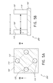
- FIG. 5A illustrates a top view of the partially formed integrated circuit of FIG. 4A after one of the masking layers has been removed in accordance with one or more embodiments of the invention.
- FIG. 5B illustrates a cross-sectional side view of the partially formed integrated circuit of FIG. 5A along the sectional line 5 B shown in FIG. 5A .
- FIG. 6A illustrates a top view of the partially formed integrated circuit of FIG. 5A during deposition of a spacer material on pillars in accordance with one or more embodiments of the invention.
- FIG. 6B illustrates a cross-sectional side view of the partially formed integrated circuit of FIG. 6A along the sectional line 6 B shown in FIG. 6A .
- FIG. 7A illustrates a top view of the partially formed integrated circuit of FIG. 6A after deposition of the spacer material in accordance with one or more embodiments of the invention.
- FIG. 7B illustrates a cross-sectional side view of the partially formed integrated circuit of FIG. 7A along the sectional line 7 B shown in FIG. 7A .
- FIG. 8A illustrates a top view of the partially formed integrated circuit of FIG. 7A after etching the spacer material in accordance with one or more embodiments of the invention.
- FIG. 8B illustrates a cross-sectional side view of the partially formed integrated circuit of FIG. 8A along the sectional line 8 B shown in FIG. 8A .
- FIG. 9A illustrates a top view of the partially formed integrated circuit of FIG. 8A after further etching the spacer material in accordance with one or more embodiments of the invention.
- FIG. 9B illustrates a cross-sectional side view of the partially formed integrated circuit of FIG. 9A along the sectional line 9 B shown in FIG. 9A .
- FIG. 10A illustrates a top view of the partially formed integrated circuit of FIG. 9A after etching the pillars in accordance with one or more embodiments of the invention.
- FIG. 10B illustrates a cross-sectional side view of the partially formed integrated circuit of FIG. 10A along the sectional line 10 B shown in FIG. 10A .
- FIG. 11A illustrates a top view of the partially formed integrated circuit of FIG. 10A after forming plugs in accordance with one or more embodiments of the invention.
- FIG. 11B illustrates a cross-sectional side view of the partially formed integrated circuit of FIG. 11A along the sectional line 11 B shown in FIG. 11A .
- FIG. 12A illustrates a top view of the partially formed integrated circuit of FIG. 11A after removing the spacer material in accordance with one or more embodiments of the invention.
- FIG. 12B illustrates a cross-sectional side view of the partially formed integrated circuit of FIG. 12A along the sectional line 12 B shown in FIG. 12A .
- Embodiments described herein provide methods of forming patterns of isolated features having a high density.
- a method for forming an integrated circuit with a pattern of features having a final density of features that is greater than a starting density of features in the integrated circuit by a multiple of two or more.
- the method can include forming a pattern of isolated pillars having a density X.
- the method can further include forming spacers around the pillars, such as by blanket depositing spacer material on and around the pillars and then isotropically etching the spacer materials to form a pattern of holes having a density at least about X.
- the pillars can be selectively removed to form a mask with a pattern of holes having a density at least about 2X.
- plugs can be formed in the pattern of holes in the mask, such as by epitaxial deposition on the substrate, in order to provide a pattern of pillars having a density at least 2X.
- the pattern of holes in the mask can be etched into the substrate to provide a pattern of holes in the substrate.
- FIG. 1A illustrates a general sequence of process steps according to some embodiments of the invention.
- a plurality of pillars are formed on a substrate, such as by etching into a layer or stack of layers formed over the substrate or by forming material over a substrate in a pattern that defines a plurality of pillars.
- the pillars can be formed by photolithography, by selectively exposing photoresist to light and then developing the photoresist to leave a pattern of pillars formed by the photoresist.
- “forming” a structure includes performing steps to make the structure or providing the structure already premade.
- step 3 spacer material is formed on and around the pillars to fill spaces between the pillars while leaving a pattern of openings between the pillars.
- step 5 the spacer material is etched to form a pattern of holes completely open to an underlying material, the holes having a density at least as great as the density of the pattern of pillars.
- step 7 the pillars are removed to form further holes, thus providing a pattern of holes with a density at least twice as great as the pattern of pillars that were previously formed on the substrate.
- FIGS. 1B-12B illustrate schematically a detailed sequence of process steps according to some embodiments of the invention.
- a substrate 100 is provided and a first hard mask layer 110 is formed thereover.
- FIG. 2 illustrates a partially formed integrated circuit 200 after step 12 has been carried out.
- the substrate 100 may include one or more of a variety of suitable workpieces for semiconductor processing.
- the substrate can include a silicon wafer.
- the first hard mask layer 110 includes amorphous carbon, e.g., transparent carbon, which has been found to have excellent etch selectivity with other materials of the illustrated imaging or masking stack. Methods for forming amorphous carbon are disclosed in A. Helmbold, D.
- a second hard mask layer 112 is also formed over the first hard mask layer 110 to protect the first hard mask layer 110 during etching in later steps and/or to enhance the accuracy of forming patterns by photolithography.
- the second hard mask layer 112 includes an anti-reflective coating (ARC), such as DARC or BARC/DARC, which can facilitate photolithography by preventing undesired light reflections.
- ARC anti-reflective coating
- a selectively definable layer 120 is formed on the second hard mask layer 112 .
- the selectively definable layer 120 can be formed using a photoresist in accordance with well-known processes for providing masks in semiconductor fabrication.
- the photoresist can be any photoresist compatible with 157 nm, 193 nm, 248 nm or 365 nm wavelength systems, 193 nm wavelength immersion systems, extreme ultraviolet systems (including 13.7 nm wavelength systems) or electron beam lithographic systems.
- maskless lithography, or maskless photolithography can be used to define the selectively definable layer 120 .
- photoresist materials include argon fluoride (ArF) sensitive photoresist, i.e., photoresist suitable for use with an ArF light source, and krypton fluoride (KrF) sensitive photoresist, i.e., photoresist suitable for use with a KrF light source.
- ArF photoresists are preferably used with photolithography systems utilizing relatively short wavelength light, e.g., 193 nm.
- KrF photoresists are preferably used with longer wavelength photolithography systems, such as 248 nm systems.
- the selectively definable layer 120 and any subsequent resist layers can be formed of a resist that can be patterned by nano-imprint lithography, e.g., by using a mold or mechanical force to pattern the resist.
- FIGS. 2A and 2B illustrate a partially formed integrated circuit 200 after step 12 has been carried out.
- the selectively definable layer 120 can include a mask pattern, the pattern including a plurality of pillars 121 having a substantially circular cross-section.
- the width of the pillars 121 in the selectively definable layer 120 is A.
- the pillars 121 can be patterned using a photolithographic technique.
- A can be substantially equal to the minimum feature size formable using the lithographic techniques.
- the pillars 121 can be formed with width A larger than the minimum formable feature size formed by photolithography and subsequently trimmed, in order to enhance the accuracy of the patterns formed by photolithography. It will be appreciated that photolithographic techniques typically can more easily and accurately form features having sizes above the size limit of the technique.
- the distance between centers of nearest neighboring pillars 121 is B.
- B is substantially equal to twice the width A, which has advantages for forming a pattern of holes arranged in rows and columns as described herein.
- the pillars 121 of the selectively definable layer 120 are trimmed during the trimming step 14 in order to achieve the dimensions C, D, and E as described hereinbelow.
- the mask pattern shown in FIGS. 2A and 2B includes pillars 121 with their centers located at the corner points of a square, other patterns are also possible, as will be described more fully hereinbelow.
- FIGS. 3A and 3B illustrate the partially formed integrated circuit 200 after step 14 of FIG. 1B has been carried out.
- the selectively definable layer 120 is trimmed, such as by subjecting the selectively definable layer 120 to O 2 /Cl 2 or O 2 /HBr plasma.
- FIG. 3B shows that after the trimming step 14 , the pillars 121 of the selectively definable layer 120 have a width C, which is less than the width A.
- the trimming step 14 can advantageously provide a feature size that is less than the minimum feature size formable using the lithographic technique used to pattern the selectively definable layer 120 .
- the width C is substantially equal to
- FIG. 3B also shows that after the trimming step 14 , the distance between two distant pillars 121 of the selectively definable layer 120 , such as between pillars 121 a and 121 c , is E.
- the distance E is substantially equal to
- FIG. 3A shows that after the trimming step 14 , the distance between neighboring pillars 121 of the selectively definable layer 120 , such as between pillars 121 a and 121 b , is D.
- the distance D is substantially equal to
- Y is used herein as a multiplier having a dimension of distance to clarify the relationship between various dimensions in the pattern of one or more embodiments.
- Y can be any real number greater than zero, including the minimum feature size formable using known lithographic techniques, and does not necessarily bear any relationship to the width A of the pillars 121 after step 12 .
- Selectively definable layers 120 having a pattern of these dimensions can produce a pattern of spacer-defined holes in later steps that is advantageously aligned with the pattern of pillars 121 in the selectively definable layer 120 .
- the pattern of the selectively definable layer 120 shown in FIG. 3A can be described as a set of pillars 121 formed in columns and rows, in which the leftmost pillar 121 a is positioned in a first column and a second row, the uppermost pillar 121 b is positioned in the second column and the first row, the lowermost pillar 121 d is positioned in the second column and a third row, and the rightmost pillar 121 c is positioned in the third column and the second row.
- FIG. 8A shows a pattern of holes 140 with a hole 140 a positioned in the first column and the first row, another hole 140 d positioned in the first column and the third row, another hole 140 c positioned in the second column and the second row, another hole 140 b positioned in the third column and the first row, and another hole 140 e positioned in the third column and the third row.
- step 16 of FIG. 1B the pattern of pillars 121 of the selectively definable layer 120 is transferred to the second hard mask layer 112 , such as by anisotropically etching the second hard mask layer 112 through the selectively definable layer 120 .
- FIGS. 4A and 4B illustrate the partially formed integrated circuit 200 after step 20 of FIG. 1B has been carried out.
- step 20 pillars 122 are formed in the first hard mask layer 110 by anisotropically etching the first hard mask layer 110 through the selectively definable layer 120 and the second hard mask layer 112 .
- the pillars 122 formed in step 20 can have substantially the same pattern as the pattern in the selectively definable layer 120 .
- the selectively definable layer 120 can be removed during or after the etching step 20 .
- the second hard mask layer 112 may be removed in step 22 , such as by carrying out a wet strip etch.
- the selectively definable layer 120 is removed by the same etch used to define pillars 122 in the first hard mask layer 110 .
- FIGS. 5A and 5B illustrate the partially formed integrated circuit 200 after removing the selectively definable layer 120 .
- spacer material 130 ( FIGS. 6A , 6 B) is deposited on the pillars 122 .
- FIGS. 6A and 6B illustrate the partially formed integrated circuit 200 while step 30 of FIG. 1B is being carried out.
- the spacer material can include an insulating material, such as an oxide, e.g., silicon oxide, particularly a material that is selectively etchable with respect to the material of the pillars 122 and other exposed surfaces. Examples of other spacer materials include silicon nitride, Al 2 O 3 , TiN, etc.
- depositing step 30 includes uniformly depositing spacer material 130 on the pillars 122 and the substrate 100 , such as by blanket depositing the spacer material 130 by chemical vapor deposition.
- FIGS. 6A and 6B show that as spacer material 130 is deposited on the pillars 122 , the spacer material 130 fills a space between neighboring pillars 122 when the spacer material 130 forms a layer having a thickness F.
- the thickness F is substantially equal to
- spacer material 130 continues to be deposited beyond filling the space between the nearest neighboring pillars 122 , such that the spacer material 130 surrounding the nearest neighboring pillars 122 converge and form voids with substantially circular cross-sections.
- the rate of deposition at the corners formed by the convergence is greater than at other parts between the pillars 122 , causing the corners of the open space between the pillars 122 to become rounded.
- FIGS. 7A and 7B illustrate the partially formed integrated circuit 200 after depositing step 30 has been carried out.
- sufficient spacer material 130 has been deposited to form holes 140 with a substantially circular cross-section.
- the holes 140 occur in a pattern that is aligned with the pattern of the pillars 122 , as described above, and the density of the holes is greater than the density of the pillars 122 in the illustrated portion of the partially formed integrated circuit.
- FIGS. 8A and 8B illustrate the partially formed integrated circuit 200 after step 32 of FIG. 1B has been carried out. As shown in FIG. 8B , after any etching to expand the holes 140 , the layer of the spacer material 130 has a thickness G and the holes 140 have been expanded to form holes 141 having a width H.
- the width H and the thickness G are both substantially equal to the width C of the pillars 122 , advantageously providing a pattern of holes 141 and pillars 122 of substantially the same size. Steps 30 and 32 of FIG. 1B can be repeated as desired in order to achieve holes 141 of the desired shapes and sizes.
- spacer material 130 ( FIGS. 9A , 9 B) is anisotropically etched to expose the upper surfaces of the pillars 122 and the substrate 100 .
- FIGS. 9A and 9B illustrate the partially formed integrated circuit 200 after step 34 of FIG. 1B has been carried out.
- the width H of the holes 141 and the thickness G of the spacer material 130 between the holes 141 and the pillars 122 remain substantially the same as before step 34 .
- the order of steps 32 and 34 can be reversed, such that the spacer material 130 is anisotropically etched before being trimmed by, e.g., an isotropic etch.
- holes having different widths may be formed.
- step 40 of FIG. 1B the pillars 122 ( FIGS. 9A , 9 B) are etched, such as by selectively etching the first hard mask layer 110 relative to the spacer material 130 to remove the pillars 122 .
- FIGS. 10A and 10B illustrate the partially formed integrated circuit 200 after step 40 of FIG. 1B has been carried out. At this stage, a pattern of holes 141 has been achieved that has a density greater than or equal to about twice the density of the features that were formed in the selectively definable layer 120 .
- the holes 141 have a smaller feature size than the pillars 121 first formed by photolithography in the selectively definable layer 120 , and the holes 141 occur in a pattern that is aligned with the pattern of pillars 121 in the selectively definable layer 120 .
- plugs 150 are formed in the holes 141 .
- FIGS. 11A and 11B illustrate the partially formed integrated circuit 200 after step 50 of FIG. 1B has been carried out.
- Plugs 150 can be formed of the same material as the substrate 100 .
- the spacer material 130 is chosen to be selectively etchable relative to the material forming the plugs 150 .
- the plugs 150 are formed of polysilicon and the spacer material 130 is formed of silicon oxide.
- Depositing step 50 can be carried out in accordance with well-known deposition processes, including but not limited to chemical vapor deposition (CVD), plasma enhanced chemical vapor deposition (PECVD), or spin coating.
- plugs 150 FIGS. 11A and 11B
- step 60 the spacer material 130 ( FIGS. 11A , 11 B) is removed, such as by selectively etching the spacer material 130 .
- the spacer material 130 FIGS. 11A , 11 B
- FIGS. 12A and 12B illustrate the partially formed integrated circuit 200 after step 60 has been carried out.
- a pattern of plugs 150 has been formed on the substrate 100 with a density greater than or equal to about twice the density of the pillars that were formed on the selectively definable layer 120 .
- the plugs 150 have a smaller feature size than the pillars 121 first formed on the selectively definable layer 120 , and the plugs 150 occur in a pattern that is aligned with the pattern of pillars 121 in the selectively definable layer 120 .
- the method described above can provide a pattern of plugs with a density greater than or equal to about twice the density of the features that were formed on the selectively definable layer 120
- the method may also be repeated to produce a pattern with a density of features that is greater than or equal to about four times the density of the original pattern.
- the method may then be repeated to achieve a pattern with a density of features that is greater than or equal to about eight times the density of the original pattern, and so on until the desired density is reached.
- the plugs 150 or pillars patterned in the substrate 100 using the layer 130 ( FIGS. 10A and 10B ) as a mask, can be used as the pillars 122 in subsequent repeats of the method.
- steps 30 - 60 may be repeated.
- isolated features having a density 2 n can be formed, where n is the number of times the method of FIGS. 1A and 1B is repeated.
- holes 141 and pillars 122 have the same size in the method described above, it may be desirable in some applications to form holes that are larger or smaller than the pillars. Accordingly, the thickness of the spacer material can be adjusted to achieve the desired result.
- the method described above provides pillars and holes with a generally circular cross section
- other shapes are also possible.
- the pillars and holes can have a cross section that is generally in the shape of a square, a rectangle, or an ellipse.
- the method described above provides holes 140 in a pattern that is aligned with the pattern of the pillars 122 , it is also possible to place the holes in other locations relative to the pillars by beginning with a pattern of pillars other than the one described above, for example a pattern in which the centers of the pillars occur at the corners of a square.
- a pattern of pillars other than the one described above, for example a pattern in which the centers of the pillars occur at the corners of a square.
- Another pattern that can be used is a pattern of three pillars, which can be used to form a hole between the three pillars.
- the embodiments described above can be used to selectively create patterns with higher density in some regions of the integrated circuit but not in other regions.
- features can be spaced apart at a distance sufficiently small that it can be filled by the thickness of the spacer material.
- features can be spaced apart at too great a distance to be filled by the spacer material and/or selectively a protective mask can be used to prevent transfer of a pattern formed by the spacer material to the substrate 110 , or to prevent deposition in the same openings formed by the spacer material 130 . In this way, a high density pattern can be selectively provided in some regions of the integrated circuit but not in others.
- an imaging stack including photoresist, an ARC, and amorphous carbon can be advantageously be applied to facilitate deposition of the spacer material. Temperatures typically used for chemical vapor deposition of the spacer material may undesirably deform photoresist, thus, amorphous carbon is used to form the pillars upon which the spacer material is deposited. In other embodiments where low temperature deposition processes (e.g., atomic layer deposition) are used to deposit the spacer material, the ARC and amorphous carbon layers may be omitted and the spacer material can be deposited on pillars formed of photoresist.
- low temperature deposition processes e.g., atomic layer deposition
- a method is provided. Such a method might include, for example, providing a substrate and forming a first set of pillars on the substrate. The method can further include depositing spacer material on the first set of pillars to form a first pattern of holes, wherein at least one of the holes is located between pillars of the first set and wherein, after depositing, spacer material fills a space between a first pillar of the first set and a nearest neighboring pillar of the first set.
- a method in other embodiments, can include providing a substrate and forming a plurality of pillars on the substrate, the pillars having a density X.
- the method can further include blanket depositing material on the pillars to form a pattern of holes on a level of the pillars, the holes having a density at least X.
- a method is provided.
- the method can include providing a substrate and forming a set of pillars on the substrate, wherein the pillars have a width of about
- the method can further include depositing material on the set of pillars.
- the method can further include etching the material to form a pattern of holes, wherein the pattern comprises a hole between the first pillar and the third pillar.
- a method can include providing a set of pillars on a substrate, the pillars arranged in two or more rows and two or more columns.
- the method can further include blanket depositing spacer material on the set of pillars to form a pattern of holes adjacent the pillars.
- the method can further include isotropically etching the spacer material to enlarge the width of the holes.
- the method can further include anisotropically etching the spacer material to expose the pillars.
Abstract
Description
Y is used herein as a multiplier having a dimension of distance to clarify the relationship between various dimensions in the pattern of one or more embodiments. Although C is substantially equal to
in
and wherein a first pillar is separated from a second pillar by a distance of about
and wherein the first pillar is separated from a third pillar by a distance of about
Claims (20)
Priority Applications (1)
| Application Number | Priority Date | Filing Date | Title |
|---|---|---|---|
| US13/690,266 US8871648B2 (en) | 2007-12-06 | 2012-11-30 | Method for forming high density patterns |
Applications Claiming Priority (3)
| Application Number | Priority Date | Filing Date | Title |
|---|---|---|---|
| US11/952,017 US7659208B2 (en) | 2007-12-06 | 2007-12-06 | Method for forming high density patterns |
| US12/686,602 US8324107B2 (en) | 2007-12-06 | 2010-01-13 | Method for forming high density patterns |
| US13/690,266 US8871648B2 (en) | 2007-12-06 | 2012-11-30 | Method for forming high density patterns |
Related Parent Applications (1)
| Application Number | Title | Priority Date | Filing Date |
|---|---|---|---|
| US12/686,602 Continuation US8324107B2 (en) | 2007-12-06 | 2010-01-13 | Method for forming high density patterns |
Publications (2)
| Publication Number | Publication Date |
|---|---|
| US20130089977A1 US20130089977A1 (en) | 2013-04-11 |
| US8871648B2 true US8871648B2 (en) | 2014-10-28 |
Family
ID=40722113
Family Applications (3)
| Application Number | Title | Priority Date | Filing Date |
|---|---|---|---|
| US11/952,017 Active 2028-01-24 US7659208B2 (en) | 2007-12-06 | 2007-12-06 | Method for forming high density patterns |
| US12/686,602 Active 2029-02-08 US8324107B2 (en) | 2007-12-06 | 2010-01-13 | Method for forming high density patterns |
| US13/690,266 Active US8871648B2 (en) | 2007-12-06 | 2012-11-30 | Method for forming high density patterns |
Family Applications Before (2)
| Application Number | Title | Priority Date | Filing Date |
|---|---|---|---|
| US11/952,017 Active 2028-01-24 US7659208B2 (en) | 2007-12-06 | 2007-12-06 | Method for forming high density patterns |
| US12/686,602 Active 2029-02-08 US8324107B2 (en) | 2007-12-06 | 2010-01-13 | Method for forming high density patterns |
Country Status (6)
| Country | Link |
|---|---|
| US (3) | US7659208B2 (en) |
| EP (1) | EP2232530A4 (en) |
| KR (1) | KR101564474B1 (en) |
| CN (1) | CN101889326B (en) |
| TW (1) | TWI505324B (en) |
| WO (1) | WO2009075959A1 (en) |
Cited By (1)
| Publication number | Priority date | Publication date | Assignee | Title |
|---|---|---|---|---|
| US10141316B2 (en) | 2016-01-08 | 2018-11-27 | Samsung Electronics Co., Ltd. | Semiconductor device with pillar and background patterns and method for fabricating the same |
Families Citing this family (41)
| Publication number | Priority date | Publication date | Assignee | Title |
|---|---|---|---|---|
| US7923373B2 (en) | 2007-06-04 | 2011-04-12 | Micron Technology, Inc. | Pitch multiplication using self-assembling materials |
| US7659208B2 (en) * | 2007-12-06 | 2010-02-09 | Micron Technology, Inc | Method for forming high density patterns |
| US7759201B2 (en) * | 2007-12-17 | 2010-07-20 | Sandisk 3D Llc | Method for fabricating pitch-doubling pillar structures |
| US7790531B2 (en) | 2007-12-18 | 2010-09-07 | Micron Technology, Inc. | Methods for isolating portions of a loop of pitch-multiplied material and related structures |
| US7887999B2 (en) * | 2007-12-27 | 2011-02-15 | Sandisk 3D Llc | Method of making a pillar pattern using triple or quadruple exposure |
| US8030218B2 (en) | 2008-03-21 | 2011-10-04 | Micron Technology, Inc. | Method for selectively modifying spacing between pitch multiplied structures |
| US7981592B2 (en) * | 2008-04-11 | 2011-07-19 | Sandisk 3D Llc | Double patterning method |
| US7786015B2 (en) * | 2008-04-28 | 2010-08-31 | Sandisk 3D Llc | Method for fabricating self-aligned complementary pillar structures and wiring |
| US7732235B2 (en) | 2008-06-30 | 2010-06-08 | Sandisk 3D Llc | Method for fabricating high density pillar structures by double patterning using positive photoresist |
| US7781269B2 (en) * | 2008-06-30 | 2010-08-24 | Sandisk 3D Llc | Triangle two dimensional complementary patterning of pillars |
| US8076208B2 (en) | 2008-07-03 | 2011-12-13 | Micron Technology, Inc. | Method for forming transistor with high breakdown voltage using pitch multiplication technique |
| US8659165B2 (en) | 2008-08-12 | 2014-02-25 | Texas Instruments Incorporated | Contact and VIA interconnects using metal around dielectric pillars |
| US8076056B2 (en) * | 2008-10-06 | 2011-12-13 | Sandisk 3D Llc | Method of making sub-resolution pillar structures using undercutting technique |
| US8492282B2 (en) | 2008-11-24 | 2013-07-23 | Micron Technology, Inc. | Methods of forming a masking pattern for integrated circuits |
| KR20100083581A (en) * | 2009-01-14 | 2010-07-22 | 삼성전자주식회사 | Methods of forming semiconductor device |
| JP5330004B2 (en) * | 2009-02-03 | 2013-10-30 | 株式会社東芝 | Manufacturing method of semiconductor device |
| EP2287670A1 (en) * | 2009-06-26 | 2011-02-23 | Rohm and Haas Electronic Materials, L.L.C. | Methods of forming electronic devices |
| US8026178B2 (en) | 2010-01-12 | 2011-09-27 | Sandisk 3D Llc | Patterning method for high density pillar structures |
| US7923305B1 (en) | 2010-01-12 | 2011-04-12 | Sandisk 3D Llc | Patterning method for high density pillar structures |
| US9054160B2 (en) | 2011-04-15 | 2015-06-09 | International Business Machines Corporation | Interconnect structure and method for fabricating on-chip interconnect structures by image reversal |
| US8890318B2 (en) | 2011-04-15 | 2014-11-18 | International Business Machines Corporation | Middle of line structures |
| US8900988B2 (en) | 2011-04-15 | 2014-12-02 | International Business Machines Corporation | Method for forming self-aligned airgap interconnect structures |
| KR101231294B1 (en) | 2011-05-31 | 2013-02-07 | 삼성에스디에스 주식회사 | Stream Controlling Method and Apparatus for Parallel Receiving of Data |
| US8822137B2 (en) * | 2011-08-03 | 2014-09-02 | International Business Machines Corporation | Self-aligned fine pitch permanent on-chip interconnect structures and method of fabrication |
| US20130062732A1 (en) | 2011-09-08 | 2013-03-14 | International Business Machines Corporation | Interconnect structures with functional components and methods for fabrication |
| US9087753B2 (en) | 2012-05-10 | 2015-07-21 | International Business Machines Corporation | Printed transistor and fabrication method |
| KR102015568B1 (en) | 2012-08-27 | 2019-08-28 | 삼성전자주식회사 | A method for forming a semiconductor memory device |
| KR102037874B1 (en) | 2013-02-07 | 2019-10-29 | 삼성전자주식회사 | Method of Forming Hole patterns of Semiconductor Devices |
| US8802551B1 (en) | 2013-02-21 | 2014-08-12 | Samsung Electronics Co., Ltd. | Methods of fabricating a semiconductor device using voids in a sacrificial layer |
| US9368348B2 (en) * | 2013-10-01 | 2016-06-14 | Taiwan Semiconductor Manufacturing Company, Ltd. | Self-aligned patterning process |
| US9177797B2 (en) * | 2013-12-04 | 2015-11-03 | Taiwan Semiconductor Manufacturing Company, Ltd. | Lithography using high selectivity spacers for pitch reduction |
| US9184059B2 (en) * | 2014-03-21 | 2015-11-10 | Inotera Memories, Inc. | Method for increasing pattern density |
| KR20160085043A (en) * | 2015-01-07 | 2016-07-15 | 에스케이하이닉스 주식회사 | Method for fabricating pattern |
| TWI640042B (en) | 2015-03-09 | 2018-11-01 | 聯華電子股份有限公司 | Manufacturing method of patterned structure of semiconductor device |
| KR102325201B1 (en) | 2015-04-22 | 2021-11-11 | 삼성전자주식회사 | Methods of manufacturing semiconductor devices |
| CN105800549B (en) * | 2016-01-16 | 2018-08-21 | 苏州工业园区纳米产业技术研究院有限公司 | Metallic nanodots array and the method for being used to form nano dot device |
| US11067895B2 (en) | 2017-01-13 | 2021-07-20 | International Business Machines Corporation | Method and structures for personalizing lithography |
| US10283362B2 (en) * | 2017-08-17 | 2019-05-07 | Nanya Technology Corporation | Method of forming fine line patterns of semiconductor devices |
| US10204783B1 (en) * | 2017-09-03 | 2019-02-12 | Nanya Technology Corporation | Method of forming fine island patterns of semiconductor devices |
| US10115594B1 (en) * | 2017-09-05 | 2018-10-30 | Nanya Technology Corporation | Method of forming fine island patterns of semiconductor devices |
| US11114299B2 (en) * | 2019-07-05 | 2021-09-07 | Applied Materials, Inc. | Techniques for reducing tip to tip shorting and critical dimension variation during nanoscale patterning |
Citations (190)
| Publication number | Priority date | Publication date | Assignee | Title |
|---|---|---|---|---|
| US4234362A (en) | 1978-11-03 | 1980-11-18 | International Business Machines Corporation | Method for forming an insulator between layers of conductive material |
| JPS5748237Y2 (en) | 1978-12-28 | 1982-10-22 | ||
| US4419809A (en) | 1981-12-30 | 1983-12-13 | International Business Machines Corporation | Fabrication process of sub-micrometer channel length MOSFETs |
| US4432132A (en) | 1981-12-07 | 1984-02-21 | Bell Telephone Laboratories, Incorporated | Formation of sidewall oxide layers by reactive oxygen ion etching to define submicron features |
| US4502914A (en) | 1982-11-13 | 1985-03-05 | International Business Machines Corporation | Method of making structures with dimensions in the sub-micrometer range |
| US4508579A (en) | 1981-03-30 | 1985-04-02 | International Business Machines Corporation | Lateral device structures using self-aligned fabrication techniques |
| US4648937A (en) | 1985-10-30 | 1987-03-10 | International Business Machines Corporation | Method of preventing asymmetric etching of lines in sub-micrometer range sidewall images transfer |
| EP0227303A2 (en) | 1985-11-25 | 1987-07-01 | Plessey Overseas Limited | Method of manufacturing semiconductor devices having side-wall isolation |
| US4716131A (en) | 1983-11-28 | 1987-12-29 | Nec Corporation | Method of manufacturing semiconductor device having polycrystalline silicon layer with metal silicide film |
| US4776922A (en) | 1987-10-30 | 1988-10-11 | International Business Machines Corporation | Formation of variable-width sidewall structures |
| US4803181A (en) | 1986-03-27 | 1989-02-07 | International Business Machines Corporation | Process for forming sub-micrometer patterns using silylation of resist side walls |
| JPS6435916U (en) | 1987-08-28 | 1989-03-03 | ||
| US4838991A (en) | 1987-10-30 | 1989-06-13 | International Business Machines Corporation | Process for defining organic sidewall structures |
| US5013680A (en) | 1990-07-18 | 1991-05-07 | Micron Technology, Inc. | Process for fabricating a DRAM array having feature widths that transcend the resolution limit of available photolithography |
| US5053105A (en) | 1990-07-19 | 1991-10-01 | Micron Technology, Inc. | Process for creating an etch mask suitable for deep plasma etches employing self-aligned silicidation of a metal layer masked with a silicon dioxide template |
| US5117027A (en) | 1990-10-31 | 1992-05-26 | Huls Aktiengesellschaft | Process for the preparation of organosilanes containing methacryloyloxy or acryloyloxy groups |
| EP0491408A3 (en) | 1990-11-20 | 1992-10-28 | Consorzio Per La Ricerca Sulla Microelettronica Nel Mezzogiorno | Process for making planarized sub-micrometric trenches in integrated circuits |
| JPH05343370A (en) | 1992-06-10 | 1993-12-24 | Toshiba Corp | Forming method for fine pattern |
| DE4236609A1 (en) | 1992-10-29 | 1994-05-05 | Siemens Ag | Method for forming a structure in the surface of a substrate - with an auxiliary structure laterally bounding an initial masking structure, followed by selective removal of masking structure using the auxiliary structure as an etching mask |
| WO1994015261A1 (en) | 1992-12-18 | 1994-07-07 | Vlsi Technology, Inc. | Method of generating lines on semiconductor wafer |
| US5328810A (en) | 1990-05-07 | 1994-07-12 | Micron Technology, Inc. | Method for reducing, by a factor or 2-N, the minimum masking pitch of a photolithographic process |
| US5330879A (en) | 1992-07-16 | 1994-07-19 | Micron Technology, Inc. | Method for fabrication of close-tolerance lines and sharp emission tips on a semiconductor wafer |
| US5470661A (en) | 1993-01-07 | 1995-11-28 | International Business Machines Corporation | Diamond-like carbon films from a hydrocarbon helium plasma |
| JPH0855908A (en) | 1994-08-17 | 1996-02-27 | Toshiba Corp | Semiconductor device |
| JPH0855920A (en) | 1994-08-15 | 1996-02-27 | Toshiba Corp | Manufacture of semiconductor device |
| US5514885A (en) | 1986-10-09 | 1996-05-07 | Myrick; James J. | SOI methods and apparatus |
| US5593813A (en) | 1994-07-14 | 1997-01-14 | Hyundai Electronics Industries Co. Ltd. | Method for forming submicroscopic patterns |
| US5670794A (en) | 1994-10-07 | 1997-09-23 | Micron Technology, Inc. | Thin film transistors |
| US5753546A (en) | 1995-06-30 | 1998-05-19 | Hyundai Electronics Industries Co., Ltd. | Method for fabricating metal oxide field effect transistors |
| US5789320A (en) | 1996-04-23 | 1998-08-04 | International Business Machines Corporation | Plating of noble metal electrodes for DRAM and FRAM |
| US5795830A (en) | 1995-06-06 | 1998-08-18 | International Business Machines Corporation | Reducing pitch with continuously adjustable line and space dimensions |
| US5830332A (en) | 1995-01-26 | 1998-11-03 | International Business Machines Corporation | Sputter deposition of hydrogenated amorphous carbon film and applications thereof |
| US5858620A (en) | 1996-07-05 | 1999-01-12 | Mitsubishi Denki Kabushiki Kaisha | Semiconductor device and method for manufacturing the same |
| KR19990001440A (en) | 1997-06-14 | 1999-01-15 | 문정환 | Wiring Formation Method of Semiconductor Device |
| US5895740A (en) | 1996-11-13 | 1999-04-20 | Vanguard International Semiconductor Corp. | Method of forming contact holes of reduced dimensions by using in-situ formed polymeric sidewall spacers |
| US5899746A (en) | 1995-09-08 | 1999-05-04 | Sony Corporation | Method of forming pattern |
| US5998256A (en) | 1996-11-01 | 1999-12-07 | Micron Technology, Inc. | Semiconductor processing methods of forming devices on a substrate, forming device arrays on a substrate, forming conductive lines on a substrate, and forming capacitor arrays on a substrate, and integrated circuitry |
| US6004862A (en) | 1998-01-20 | 1999-12-21 | Advanced Micro Devices, Inc. | Core array and periphery isolation technique |
| US6010946A (en) | 1996-08-21 | 2000-01-04 | Nec Corporation | Semiconductor device with isolation insulating film tapered and method of manufacturing the same |
| US6020255A (en) | 1998-07-13 | 2000-02-01 | Taiwan Semiconductor Manufacturing Company | Dual damascene interconnect process with borderless contact |
| US6042998A (en) | 1993-09-30 | 2000-03-28 | The University Of New Mexico | Method and apparatus for extending spatial frequencies in photolithography images |
| US6057573A (en) | 1998-05-27 | 2000-05-02 | Vanguard International Semiconductor Corporation | Design for high density memory with relaxed metal pitch |
| US6063688A (en) | 1997-09-29 | 2000-05-16 | Intel Corporation | Fabrication of deep submicron structures and quantum wire transistors using hard-mask transistor width definition |
| US6071789A (en) | 1998-11-10 | 2000-06-06 | Vanguard International Semiconductor Corporation | Method for simultaneously fabricating a DRAM capacitor and metal interconnections |
| JP2000208434A (en) | 1999-01-06 | 2000-07-28 | Infineon Technol North America Corp | Patterning method of semiconductor element and semiconductor device |
| US6110837A (en) | 1999-04-28 | 2000-08-29 | Worldwide Semiconductor Manufacturing Corp. | Method for forming a hard mask of half critical dimension |
| US6143476A (en) | 1997-12-12 | 2000-11-07 | Applied Materials Inc | Method for high temperature etching of patterned layers using an organic mask stack |
| JP2000357736A (en) | 1999-06-15 | 2000-12-26 | Toshiba Corp | Semiconductor device and manufacture thereof |
| US6207490B1 (en) | 1997-12-11 | 2001-03-27 | Samsung Electronics Co., Ltd. | Semiconductor device and method for fabricating the same |
| US6211044B1 (en) | 1999-04-12 | 2001-04-03 | Advanced Micro Devices | Process for fabricating a semiconductor device component using a selective silicidation reaction |
| US6288454B1 (en) | 1999-05-13 | 2001-09-11 | Lsi Logic Corporation | Semiconductor wafer having a layer-to-layer alignment mark and method for fabricating the same |
| US6291334B1 (en) | 1997-12-19 | 2001-09-18 | Applied Materials, Inc. | Etch stop layer for dual damascene process |
| US6297554B1 (en) | 2000-03-10 | 2001-10-02 | United Microelectronics Corp. | Dual damascene interconnect structure with reduced parasitic capacitance |
| US6335257B1 (en) | 2000-09-29 | 2002-01-01 | Vanguard International Semiconductor Corporation | Method of making pillar-type structure on semiconductor substrate |
| US6348380B1 (en) | 2000-08-25 | 2002-02-19 | Micron Technology, Inc. | Use of dilute steam ambient for improvement of flash devices |
| US6362057B1 (en) | 1999-10-26 | 2002-03-26 | Motorola, Inc. | Method for forming a semiconductor device |
| US20020042198A1 (en) | 2000-09-20 | 2002-04-11 | Bjarni Bjarnason | Method in etching of a substrate |
| US20020045308A1 (en) | 1996-11-01 | 2002-04-18 | Werner Juengling | Semiconductor processing methods of forming a plurality of capacitors on a substrate, bit line contacts and method of forming bit line contacts |
| US6383907B1 (en) | 1999-09-08 | 2002-05-07 | Sony Corporation | Process for fabricating a semiconductor device |
| US20020063110A1 (en) | 2000-11-30 | 2002-05-30 | Cantell Marc W. | Etching of hard masks |
| US20020068243A1 (en) | 2000-12-04 | 2002-06-06 | Jiunn-Ren Hwang | Method of forming opening in wafer layer |
| US20020094688A1 (en) | 2001-01-16 | 2002-07-18 | Semiconductor Leading Edge Technologies, Inc. | Method of forming fine patterns |
| US6423474B1 (en) | 2000-03-21 | 2002-07-23 | Micron Technology, Inc. | Use of DARC and BARC in flash memory processing |
| US20020127810A1 (en) | 2000-05-29 | 2002-09-12 | Fujitsu Limited | Semiconductor device and method for fabricating the same |
| US6455372B1 (en) | 2000-08-14 | 2002-09-24 | Micron Technology, Inc. | Nucleation for improved flash erase characteristics |
| WO2002099864A1 (en) | 2001-05-31 | 2002-12-12 | Infineon Technologies, Ag | Method for removing polysilane from a semiconductor without stripping |
| US6500756B1 (en) | 2002-06-28 | 2002-12-31 | Advanced Micro Devices, Inc. | Method of forming sub-lithographic spaces between polysilicon lines |
| US20030006410A1 (en) | 2000-03-01 | 2003-01-09 | Brian Doyle | Quantum wire gate device and method of making same |
| US6514884B2 (en) | 1998-02-06 | 2003-02-04 | Semiconductor Process Laboratory Co., Ltd. | Method for reforming base surface, method for manufacturing semiconductor device and equipment for manufacturing the same |
| US6522584B1 (en) | 2001-08-02 | 2003-02-18 | Micron Technology, Inc. | Programming methods for multi-level flash EEPROMs |
| US20030044722A1 (en) | 2001-08-28 | 2003-03-06 | Yi-Yu Hsu | Process for improving critical dimension uniformity |
| US6534243B1 (en) | 2000-10-23 | 2003-03-18 | Advanced Micro Devices, Inc. | Chemical feature doubling process |
| US6548396B2 (en) | 1998-07-23 | 2003-04-15 | Applied Materials, Inc. | Method of producing an interconnect structure for an integrated circuit |
| US6559017B1 (en) | 2002-06-13 | 2003-05-06 | Advanced Micro Devices, Inc. | Method of using amorphous carbon as spacer material in a disposable spacer process |
| US6566280B1 (en) | 2002-08-26 | 2003-05-20 | Intel Corporation | Forming polymer features on a substrate |
| US6573030B1 (en) | 2000-02-17 | 2003-06-03 | Applied Materials, Inc. | Method for depositing an amorphous carbon layer |
| US20030109102A1 (en) | 2001-10-24 | 2003-06-12 | Hiroshi Kujirai | Method of manufacturing semiconductor device and semiconductor device |
| US20030119307A1 (en) | 2001-12-26 | 2003-06-26 | Applied Materials, Inc. | Method of forming a dual damascene structure |
| US20030127426A1 (en) | 2002-01-07 | 2003-07-10 | Macronix International Co., Ltd. | Method for pitch reduction |
| US6602779B1 (en) | 2002-05-13 | 2003-08-05 | Taiwan Semiconductor Manufacturing Co., Ltd | Method for forming low dielectric constant damascene structure while employing carbon doped silicon oxide planarizing stop layer |
| US20030157436A1 (en) | 2002-02-20 | 2003-08-21 | Dirk Manger | Method for forming a hard mask in a layer on a planar device |
| US6620715B1 (en) | 2002-03-29 | 2003-09-16 | Cypress Semiconductor Corp. | Method for forming sub-critical dimension structures in an integrated circuit |
| US6632741B1 (en) | 2000-07-19 | 2003-10-14 | International Business Machines Corporation | Self-trimming method on looped patterns |
| US20030207207A1 (en) | 2002-05-03 | 2003-11-06 | Weimin Li | Method of fabricating a semiconductor multilevel interconnect structure |
| US20030207584A1 (en) | 2002-05-01 | 2003-11-06 | Swaminathan Sivakumar | Patterning tighter and looser pitch geometries |
| US20030216050A1 (en) | 2002-05-17 | 2003-11-20 | International Business Machines Corporation | Method of forming active devices of different gatelengths using lithographic printed gate images of same length |
| US20030215978A1 (en) | 2001-09-19 | 2003-11-20 | Jon Maimon | Method for making tapered opening for programmable resistance memory element |
| US20030230234A1 (en) | 2002-06-14 | 2003-12-18 | Dong-Seok Nam | Method of forming fine patterns of semiconductor device |
| US6667237B1 (en) | 2000-10-12 | 2003-12-23 | Vram Technologies, Llc | Method and apparatus for patterning fine dimensions |
| WO2004001799A2 (en) | 2002-06-20 | 2003-12-31 | Applied Materials, Inc. | Method for fabricating a gate structure of a field effect transistor |
| US20040000534A1 (en) | 2002-06-28 | 2004-01-01 | Infineon Technologies North America Corp. | Hardmask of amorphous carbon-hydrogen (a-C:H) layers with tunable etch resistivity |
| US6673684B1 (en) | 2002-07-31 | 2004-01-06 | Advanced Micro Devices, Inc. | Use of diamond as a hard mask material |
| WO2004003977A2 (en) | 2002-06-27 | 2004-01-08 | Advanced Micro Devices, Inc. | Method of defining the dimensions of circuit elements by using spacer deposition techniques |
| US20040018738A1 (en) | 2002-07-22 | 2004-01-29 | Wei Liu | Method for fabricating a notch gate structure of a field effect transistor |
| US20040017989A1 (en) | 2002-07-23 | 2004-01-29 | So Daniel W. | Fabricating sub-resolution structures in planar lightwave devices |
| US6686245B1 (en) | 2002-12-20 | 2004-02-03 | Motorola, Inc. | Vertical MOSFET with asymmetric gate structure |
| US20040023502A1 (en) | 2002-08-02 | 2004-02-05 | Applied Materials Inc. | Undoped and fluorinated amorphous carbon film as pattern mask for metal etch |
| US20040023475A1 (en) | 2002-07-31 | 2004-02-05 | Advanced Micro Devices, Inc. | Method for reducing pattern deformation and photoresist poisoning in semiconductor device fabrication |
| US6689695B1 (en) | 2002-06-28 | 2004-02-10 | Taiwan Semiconductor Manufacturing Company | Multi-purpose composite mask for dual damascene patterning |
| JP2004080033A (en) | 2002-08-09 | 2004-03-11 | Samsung Electronics Co Ltd | Method of micropattern formation using silicon oxide film |
| US6706571B1 (en) | 2002-10-22 | 2004-03-16 | Advanced Micro Devices, Inc. | Method for forming multiple structures in a semiconductor device |
| US20040053475A1 (en) | 2002-09-18 | 2004-03-18 | Gian Sharma | Method for forming a sublithographic opening in a semiconductor process |
| US6709807B2 (en) | 1999-12-02 | 2004-03-23 | Axcelis Technologies, Inc. | Process for reducing edge roughness in patterned photoresist |
| US20040079988A1 (en) | 2002-10-28 | 2004-04-29 | Sandisk Corporation | Flash memory cell arrays having dual control gates per memory cell charge storage element |
| US6734107B2 (en) | 2002-06-12 | 2004-05-11 | Macronix International Co., Ltd. | Pitch reduction in semiconductor fabrication |
| JP2004152784A (en) | 2002-10-28 | 2004-05-27 | Fujitsu Ltd | Method for manufacturing fine pattern and method for manufacturing semiconductor device |
| US6744094B2 (en) | 2001-08-24 | 2004-06-01 | Micron Technology Inc. | Floating gate transistor with horizontal gate layers stacked next to vertical body |
| US20040106257A1 (en) | 2002-04-12 | 2004-06-03 | Matsushita Electric Industrial Co., Ltd. | Method for fabricating semiconductor device |
| EP1357433A3 (en) | 2002-04-23 | 2004-06-23 | Hewlett-Packard Company | Method of fabricating sub-lithographic sized line and space patterns |
| US6762449B2 (en) | 1999-04-23 | 2004-07-13 | Hitachi, Ltd. | Semiconductor integrated circuit device and the process of manufacturing the same having poly-silicon plug, wiring trenches and bit lines formed in the wiring trenches having a width finer than a predetermined size |
| US6773998B1 (en) | 2003-05-20 | 2004-08-10 | Advanced Micro Devices, Inc. | Modified film stack and patterning strategy for stress compensation and prevention of pattern distortion in amorphous carbon gate patterning |
| US6818141B1 (en) | 2002-06-10 | 2004-11-16 | Advanced Micro Devices, Inc. | Application of the CVD bilayer ARC as a hard mask for definition of the subresolution trench features between polysilicon wordlines |
| US20040235255A1 (en) | 2003-05-21 | 2004-11-25 | Renesas Technology Corp. | Method of manufacturing semiconductor device capable of suppressing impurity concentration reduction in doped channel region arising from formation of gate insulating film |
| US6835662B1 (en) | 2003-07-14 | 2004-12-28 | Advanced Micro Devices, Inc. | Partially de-coupled core and periphery gate module process |
| US6867116B1 (en) | 2003-11-10 | 2005-03-15 | Macronix International Co., Ltd. | Fabrication method of sub-resolution pitch for integrated circuits |
| US6875703B1 (en) | 2004-01-20 | 2005-04-05 | International Business Machines Corporation | Method for forming quadruple density sidewall image transfer (SIT) structures |
| US20050074949A1 (en) | 2003-10-01 | 2005-04-07 | Dongbu Electronics Co., Ltd. | Semiconductor device and a method for fabricating the semiconductor device |
| WO2005034215A1 (en) | 2003-09-30 | 2005-04-14 | Infineon Technologies Ag | Method for the production of a hard mask and hard mask arrangement |
| US6893972B2 (en) | 2001-08-31 | 2005-05-17 | Infineon Technologies Ag | Process for sidewall amplification of resist structures and for the production of structures having reduced structure size |
| US20050112886A1 (en) | 2001-12-28 | 2005-05-26 | Kabushiki Kaisha Toshiba | Light-emitting device and method for manufacturing the same |
| JP2005150333A (en) | 2003-11-14 | 2005-06-09 | Sony Corp | Method of manufacturing semiconductor device |
| US20050142497A1 (en) | 2003-12-26 | 2005-06-30 | Samsung Electronics Co., Ltd. | Method of forming a pattern in a semiconductor device and method of forming a gate using the same |
| US6916594B2 (en) | 2002-12-30 | 2005-07-12 | Hynix Semiconductor Inc. | Overcoating composition for photoresist and method for forming photoresist pattern using the same |
| US20050153562A1 (en) | 2004-01-08 | 2005-07-14 | Toshiharu Furukawa | Method of independent P and N gate length control of FET device made by sidewall image transfer technique |
| US20050167394A1 (en) | 2004-01-30 | 2005-08-04 | Wei Liu | Techniques for the use of amorphous carbon (APF) for various etch and litho integration scheme |
| US20050186705A1 (en) | 2002-07-31 | 2005-08-25 | Jackson Timothy L. | Semiconductor dice having backside redistribution layer accessed using through-silicon vias, methods |
| US6955961B1 (en) | 2004-05-27 | 2005-10-18 | Macronix International Co., Ltd. | Method for defining a minimum pitch in an integrated circuit beyond photolithographic resolution |
| US20050272259A1 (en) | 2004-06-08 | 2005-12-08 | Macronix International Co., Ltd. | Method of pitch dimension shrinkage |
| US20060003182A1 (en) | 2004-07-01 | 2006-01-05 | Lane Richard H | Method for forming controlled geometry hardmasks including subresolution elements and resulting structures |
| US20060011947A1 (en) | 2004-05-26 | 2006-01-19 | Werner Juengling | Semiconductor structures and memory device constructions |
| US20060024945A1 (en) | 2004-07-29 | 2006-02-02 | Hynix Semiconductor, Inc. | Method for fabricating semiconductor device using amorphous carbon layer as sacrificial hard mask |
| US20060024940A1 (en) | 2004-07-28 | 2006-02-02 | International Business Machines Corporation | Borderless contact structures |
| US20060046484A1 (en) | 2004-09-02 | 2006-03-02 | Abatchev Mirzafer K | Method for integrated circuit fabrication using pitch multiplication |
| US20060046200A1 (en) | 2004-09-01 | 2006-03-02 | Abatchev Mirzafer K | Mask material conversion |
| US20060046201A1 (en) | 2004-09-02 | 2006-03-02 | Sandhu Gurtej S | Method to align mask patterns |
| US20060046161A1 (en) | 2004-08-31 | 2006-03-02 | Zhiping Yin | Prevention of photoresist scumming |
| US20060046422A1 (en) | 2004-08-31 | 2006-03-02 | Micron Technology, Inc. | Methods for increasing photo alignment margins |
| US7015124B1 (en) | 2003-04-28 | 2006-03-21 | Advanced Micro Devices, Inc. | Use of amorphous carbon for gate patterning |
| US20060083996A1 (en) | 2004-10-11 | 2006-04-20 | Ho-Chul Kim | Apparatus for exposing a substrate, photomask and modified illuminating system of the apparatus, and method of forming a pattern on a substrate using the apparatus |
| US20060115978A1 (en) | 2004-11-30 | 2006-06-01 | Michael Specht | Charge-trapping memory cell and method for production |
| US7074668B1 (en) | 2004-12-16 | 2006-07-11 | Hynix Semiconductor Inc. | Capacitor of semiconductor device and method for forming the same |
| US20060172540A1 (en) | 2005-02-03 | 2006-08-03 | Jeffrey Marks | Reduction of feature critical dimensions using multiple masks |
| US20060189150A1 (en) | 2005-02-23 | 2006-08-24 | Hynix Semiconductor Inc. | Composition for an organic hard mask and method for forming a pattern on a semiconductor device using the same |
| US20060211260A1 (en) | 2005-03-15 | 2006-09-21 | Luan Tran | Pitch reduced patterns relative to photolithography features |
| US20060216923A1 (en) | 2005-03-28 | 2006-09-28 | Tran Luan C | Integrated circuit fabrication |
| US20060231900A1 (en) | 2005-04-19 | 2006-10-19 | Ji-Young Lee | Semiconductor device having fine contacts and method of fabricating the same |
| US20060263699A1 (en) | 2005-05-23 | 2006-11-23 | Mirzafer Abatchev | Methods for forming arrays of a small, closely spaced features |
| US20060267075A1 (en) | 2005-05-26 | 2006-11-30 | Micron Technology, Inc. | Multi-state memory cell |
| US20060273456A1 (en) | 2005-06-02 | 2006-12-07 | Micron Technology, Inc., A Corporation | Multiple spacer steps for pitch multiplication |
| US20060281266A1 (en) | 2005-06-09 | 2006-12-14 | Wells David H | Method and apparatus for adjusting feature size and position |
| JP2006351861A (en) | 2005-06-16 | 2006-12-28 | Toshiba Corp | Manufacturing method of semiconductor device |
| US20070018345A1 (en) | 2005-07-25 | 2007-01-25 | Bing-Huan Lee | Nanoimprint lithograph for fabricating nanoadhesive |
| US20070026672A1 (en) | 2005-07-29 | 2007-02-01 | Micron Technology, Inc. | Pitch doubled circuit layout |
| US7183142B2 (en) | 2005-01-13 | 2007-02-27 | International Business Machines Corporation | FinFETs with long gate length at high density |
| US20070049011A1 (en) | 2005-09-01 | 2007-03-01 | Micron Technology, Inc., A Corporation | Method of forming isolated features using pitch multiplication |
| US20070049035A1 (en) | 2005-08-31 | 2007-03-01 | Tran Luan C | Method of forming pitch multipled contacts |
| US20070049030A1 (en) | 2005-09-01 | 2007-03-01 | Sandhu Gurtej S | Pitch multiplication spacers and methods of forming the same |
| US20070049032A1 (en) | 2005-09-01 | 2007-03-01 | Mirzafer Abatchev | Protective coating for planarization |
| US20070048674A1 (en) | 2005-09-01 | 2007-03-01 | Wells David H | Methods for forming arrays of small, closely spaced features |
| US20070049040A1 (en) | 2005-03-15 | 2007-03-01 | Micron Technology, Inc., A Corporation | Multiple deposition for integration of spacers in pitch multiplication process |
| US20070045712A1 (en) | 2005-09-01 | 2007-03-01 | Haller Gordon A | Memory cell layout and process flow |
| US20070050748A1 (en) | 2005-08-30 | 2007-03-01 | Micron Technology, Inc., A Corporation | Method and algorithm for random half pitched interconnect layout with constant spacing |
| US20070077524A1 (en) | 2005-09-30 | 2007-04-05 | Samsung Electronics Co., Ltd. | Method for forming patterns of semiconductor device |
| US7202174B1 (en) | 2006-02-02 | 2007-04-10 | Hynix Semiconductor Inc. | Method of forming micro pattern in semiconductor device |
| US7208379B2 (en) | 2004-11-29 | 2007-04-24 | Texas Instruments Incorporated | Pitch multiplication process |
| US20070148968A1 (en) | 2005-12-26 | 2007-06-28 | Samsung Electronics Co., Ltd. | Method of forming self-aligned double pattern |
| US20070205438A1 (en) | 2006-03-02 | 2007-09-06 | Werner Juengling | Masking process for simultaneously patterning separate regions |
| US20070210449A1 (en) | 2006-03-07 | 2007-09-13 | Dirk Caspary | Memory device and an array of conductive lines and methods of making the same |
| US20070215960A1 (en) | 2004-03-19 | 2007-09-20 | The Regents Of The University Of California | Methods for Fabrication of Positional and Compositionally Controlled Nanostructures on Substrate |
| US20070215874A1 (en) | 2006-03-17 | 2007-09-20 | Toshiharu Furukawa | Layout and process to contact sub-lithographic structures |
| US20070238308A1 (en) | 2006-04-07 | 2007-10-11 | Ardavan Niroomand | Simplified pitch doubling process flow |
| US20070249170A1 (en) | 2006-04-25 | 2007-10-25 | David Kewley | Process for improving critical dimension uniformity of integrated circuit arrays |
| US7288445B2 (en) | 2001-06-21 | 2007-10-30 | International Business Machines Corporation | Double gated transistor and method of fabrication |
| US7291560B2 (en) | 2005-08-01 | 2007-11-06 | Infineon Technologies Ag | Method of production pitch fractionizations in semiconductor technology |
| US20070261016A1 (en) | 2006-04-24 | 2007-11-08 | Sandhu Gurtej S | Masking techniques and templates for dense semiconductor fabrication |
| US20070275309A1 (en) | 2006-05-24 | 2007-11-29 | Synopsys, Inc. | Patterning A Single Integrated Circuit Layer Using Multiple Masks And Multiple Masking Layers |
| US20070281219A1 (en) | 2006-06-01 | 2007-12-06 | Sandhu Gurtej S | Masking techniques and contact imprint reticles for dense semiconductor fabrication |
| US20080057692A1 (en) | 2006-08-30 | 2008-03-06 | Wells David H | Single spacer process for multiplying pitch by a factor greater than two and related intermediate IC structures |
| US20080054350A1 (en) | 2006-09-06 | 2008-03-06 | International Business Machines Corporation | Vertical field effect transistor arrays and methods for fabrication thereof |
| US20080070165A1 (en) | 2006-09-14 | 2008-03-20 | Mark Fischer | Efficient pitch multiplication process |
| US7378727B2 (en) | 2005-09-30 | 2008-05-27 | Dirk Caspary | Memory device and a method of forming a memory device |
| US7442976B2 (en) | 2004-09-01 | 2008-10-28 | Micron Technology, Inc. | DRAM cells with vertical transistors |
| US7456458B2 (en) | 2006-01-11 | 2008-11-25 | Promos Technologies Inc. | Dynamic random access memory structure |
| US20080292991A1 (en) | 2007-05-24 | 2008-11-27 | Advanced Micro Devices, Inc. | High fidelity multiple resist patterning |
| US20080299774A1 (en) | 2007-06-04 | 2008-12-04 | Micron Technology, Inc. | Pitch multiplication using self-assembling materials |
| US20090035665A1 (en) | 2007-07-31 | 2009-02-05 | Micron Technology, Inc. | Process of semiconductor fabrication with mask overlay on pitch multiplied features and associated structures |
| US20090115064A1 (en) | 2007-11-01 | 2009-05-07 | Micron Technology, Inc. | Spacer process for on pitch contacts and related structures |
| US7659208B2 (en) * | 2007-12-06 | 2010-02-09 | Micron Technology, Inc | Method for forming high density patterns |
| US7659205B2 (en) | 2004-07-27 | 2010-02-09 | Micron Technology, Inc. | Amorphous carbon-based non-volatile memory |
| US7851135B2 (en) | 2007-11-30 | 2010-12-14 | Hynix Semiconductor Inc. | Method of forming an etching mask pattern from developed negative and positive photoresist layers |
Family Cites Families (4)
| Publication number | Priority date | Publication date | Assignee | Title |
|---|---|---|---|---|
| JP2805702B2 (en) * | 1987-07-24 | 1998-09-30 | ソニー株式会社 | Semiconductor memory device |
| US5933742A (en) * | 1996-09-06 | 1999-08-03 | Powerchip Semiconductor Corp. | Multi-crown capacitor for high density DRAMS |
| US6204115B1 (en) * | 1999-06-03 | 2001-03-20 | Stanford University | Manufacture of high-density pillar memory cell arrangement |
| KR100399436B1 (en) * | 2001-03-28 | 2003-09-29 | 주식회사 하이닉스반도체 | A Magnetic random access memory and a method for manufacturing the same |
-
2007
- 2007-12-06 US US11/952,017 patent/US7659208B2/en active Active
-
2008
- 2008-10-28 WO PCT/US2008/081474 patent/WO2009075959A1/en active Application Filing
- 2008-10-28 KR KR1020107014880A patent/KR101564474B1/en active IP Right Grant
- 2008-10-28 CN CN200880119291.9A patent/CN101889326B/en active Active
- 2008-10-28 EP EP08858925.4A patent/EP2232530A4/en not_active Withdrawn
- 2008-11-11 TW TW097143566A patent/TWI505324B/en active
-
2010
- 2010-01-13 US US12/686,602 patent/US8324107B2/en active Active
-
2012
- 2012-11-30 US US13/690,266 patent/US8871648B2/en active Active
Patent Citations (203)
| Publication number | Priority date | Publication date | Assignee | Title |
|---|---|---|---|---|
| US4234362A (en) | 1978-11-03 | 1980-11-18 | International Business Machines Corporation | Method for forming an insulator between layers of conductive material |
| JPS5748237Y2 (en) | 1978-12-28 | 1982-10-22 | ||
| US4508579A (en) | 1981-03-30 | 1985-04-02 | International Business Machines Corporation | Lateral device structures using self-aligned fabrication techniques |
| US4432132A (en) | 1981-12-07 | 1984-02-21 | Bell Telephone Laboratories, Incorporated | Formation of sidewall oxide layers by reactive oxygen ion etching to define submicron features |
| US4419809A (en) | 1981-12-30 | 1983-12-13 | International Business Machines Corporation | Fabrication process of sub-micrometer channel length MOSFETs |
| US4502914A (en) | 1982-11-13 | 1985-03-05 | International Business Machines Corporation | Method of making structures with dimensions in the sub-micrometer range |
| US4716131A (en) | 1983-11-28 | 1987-12-29 | Nec Corporation | Method of manufacturing semiconductor device having polycrystalline silicon layer with metal silicide film |
| US4648937A (en) | 1985-10-30 | 1987-03-10 | International Business Machines Corporation | Method of preventing asymmetric etching of lines in sub-micrometer range sidewall images transfer |
| EP0227303A2 (en) | 1985-11-25 | 1987-07-01 | Plessey Overseas Limited | Method of manufacturing semiconductor devices having side-wall isolation |
| US4803181A (en) | 1986-03-27 | 1989-02-07 | International Business Machines Corporation | Process for forming sub-micrometer patterns using silylation of resist side walls |
| US5514885A (en) | 1986-10-09 | 1996-05-07 | Myrick; James J. | SOI methods and apparatus |
| JPS6435916U (en) | 1987-08-28 | 1989-03-03 | ||
| US4776922A (en) | 1987-10-30 | 1988-10-11 | International Business Machines Corporation | Formation of variable-width sidewall structures |
| US4838991A (en) | 1987-10-30 | 1989-06-13 | International Business Machines Corporation | Process for defining organic sidewall structures |
| US5328810A (en) | 1990-05-07 | 1994-07-12 | Micron Technology, Inc. | Method for reducing, by a factor or 2-N, the minimum masking pitch of a photolithographic process |
| US5013680A (en) | 1990-07-18 | 1991-05-07 | Micron Technology, Inc. | Process for fabricating a DRAM array having feature widths that transcend the resolution limit of available photolithography |
| US5053105A (en) | 1990-07-19 | 1991-10-01 | Micron Technology, Inc. | Process for creating an etch mask suitable for deep plasma etches employing self-aligned silicidation of a metal layer masked with a silicon dioxide template |
| US5117027A (en) | 1990-10-31 | 1992-05-26 | Huls Aktiengesellschaft | Process for the preparation of organosilanes containing methacryloyloxy or acryloyloxy groups |
| EP0491408A3 (en) | 1990-11-20 | 1992-10-28 | Consorzio Per La Ricerca Sulla Microelettronica Nel Mezzogiorno | Process for making planarized sub-micrometric trenches in integrated circuits |
| JPH05343370A (en) | 1992-06-10 | 1993-12-24 | Toshiba Corp | Forming method for fine pattern |
| US5330879A (en) | 1992-07-16 | 1994-07-19 | Micron Technology, Inc. | Method for fabrication of close-tolerance lines and sharp emission tips on a semiconductor wafer |
| DE4236609A1 (en) | 1992-10-29 | 1994-05-05 | Siemens Ag | Method for forming a structure in the surface of a substrate - with an auxiliary structure laterally bounding an initial masking structure, followed by selective removal of masking structure using the auxiliary structure as an etching mask |
| WO1994015261A1 (en) | 1992-12-18 | 1994-07-07 | Vlsi Technology, Inc. | Method of generating lines on semiconductor wafer |
| US5470661A (en) | 1993-01-07 | 1995-11-28 | International Business Machines Corporation | Diamond-like carbon films from a hydrocarbon helium plasma |
| US6042998A (en) | 1993-09-30 | 2000-03-28 | The University Of New Mexico | Method and apparatus for extending spatial frequencies in photolithography images |
| US5593813A (en) | 1994-07-14 | 1997-01-14 | Hyundai Electronics Industries Co. Ltd. | Method for forming submicroscopic patterns |
| JPH0855920A (en) | 1994-08-15 | 1996-02-27 | Toshiba Corp | Manufacture of semiconductor device |
| JPH0855908A (en) | 1994-08-17 | 1996-02-27 | Toshiba Corp | Semiconductor device |
| US5670794A (en) | 1994-10-07 | 1997-09-23 | Micron Technology, Inc. | Thin film transistors |
| US5830332A (en) | 1995-01-26 | 1998-11-03 | International Business Machines Corporation | Sputter deposition of hydrogenated amorphous carbon film and applications thereof |
| US5795830A (en) | 1995-06-06 | 1998-08-18 | International Business Machines Corporation | Reducing pitch with continuously adjustable line and space dimensions |
| US5753546A (en) | 1995-06-30 | 1998-05-19 | Hyundai Electronics Industries Co., Ltd. | Method for fabricating metal oxide field effect transistors |
| US5899746A (en) | 1995-09-08 | 1999-05-04 | Sony Corporation | Method of forming pattern |
| US5789320A (en) | 1996-04-23 | 1998-08-04 | International Business Machines Corporation | Plating of noble metal electrodes for DRAM and FRAM |
| US5858620A (en) | 1996-07-05 | 1999-01-12 | Mitsubishi Denki Kabushiki Kaisha | Semiconductor device and method for manufacturing the same |
| US6010946A (en) | 1996-08-21 | 2000-01-04 | Nec Corporation | Semiconductor device with isolation insulating film tapered and method of manufacturing the same |
| US5998256A (en) | 1996-11-01 | 1999-12-07 | Micron Technology, Inc. | Semiconductor processing methods of forming devices on a substrate, forming device arrays on a substrate, forming conductive lines on a substrate, and forming capacitor arrays on a substrate, and integrated circuitry |
| US20020045308A1 (en) | 1996-11-01 | 2002-04-18 | Werner Juengling | Semiconductor processing methods of forming a plurality of capacitors on a substrate, bit line contacts and method of forming bit line contacts |
| US5895740A (en) | 1996-11-13 | 1999-04-20 | Vanguard International Semiconductor Corp. | Method of forming contact holes of reduced dimensions by using in-situ formed polymeric sidewall spacers |
| KR19990001440A (en) | 1997-06-14 | 1999-01-15 | 문정환 | Wiring Formation Method of Semiconductor Device |
| US6063688A (en) | 1997-09-29 | 2000-05-16 | Intel Corporation | Fabrication of deep submicron structures and quantum wire transistors using hard-mask transistor width definition |
| US6207490B1 (en) | 1997-12-11 | 2001-03-27 | Samsung Electronics Co., Ltd. | Semiconductor device and method for fabricating the same |
| US6143476A (en) | 1997-12-12 | 2000-11-07 | Applied Materials Inc | Method for high temperature etching of patterned layers using an organic mask stack |
| US6291334B1 (en) | 1997-12-19 | 2001-09-18 | Applied Materials, Inc. | Etch stop layer for dual damascene process |
| US6004862A (en) | 1998-01-20 | 1999-12-21 | Advanced Micro Devices, Inc. | Core array and periphery isolation technique |
| US6514884B2 (en) | 1998-02-06 | 2003-02-04 | Semiconductor Process Laboratory Co., Ltd. | Method for reforming base surface, method for manufacturing semiconductor device and equipment for manufacturing the same |
| US6057573A (en) | 1998-05-27 | 2000-05-02 | Vanguard International Semiconductor Corporation | Design for high density memory with relaxed metal pitch |
| US6020255A (en) | 1998-07-13 | 2000-02-01 | Taiwan Semiconductor Manufacturing Company | Dual damascene interconnect process with borderless contact |
| US6548396B2 (en) | 1998-07-23 | 2003-04-15 | Applied Materials, Inc. | Method of producing an interconnect structure for an integrated circuit |
| US6071789A (en) | 1998-11-10 | 2000-06-06 | Vanguard International Semiconductor Corporation | Method for simultaneously fabricating a DRAM capacitor and metal interconnections |
| JP2000208434A (en) | 1999-01-06 | 2000-07-28 | Infineon Technol North America Corp | Patterning method of semiconductor element and semiconductor device |
| US6211044B1 (en) | 1999-04-12 | 2001-04-03 | Advanced Micro Devices | Process for fabricating a semiconductor device component using a selective silicidation reaction |
| US6762449B2 (en) | 1999-04-23 | 2004-07-13 | Hitachi, Ltd. | Semiconductor integrated circuit device and the process of manufacturing the same having poly-silicon plug, wiring trenches and bit lines formed in the wiring trenches having a width finer than a predetermined size |
| US6110837A (en) | 1999-04-28 | 2000-08-29 | Worldwide Semiconductor Manufacturing Corp. | Method for forming a hard mask of half critical dimension |
| US6288454B1 (en) | 1999-05-13 | 2001-09-11 | Lsi Logic Corporation | Semiconductor wafer having a layer-to-layer alignment mark and method for fabricating the same |
| JP2000357736A (en) | 1999-06-15 | 2000-12-26 | Toshiba Corp | Semiconductor device and manufacture thereof |
| US6383907B1 (en) | 1999-09-08 | 2002-05-07 | Sony Corporation | Process for fabricating a semiconductor device |
| US6362057B1 (en) | 1999-10-26 | 2002-03-26 | Motorola, Inc. | Method for forming a semiconductor device |
| US6709807B2 (en) | 1999-12-02 | 2004-03-23 | Axcelis Technologies, Inc. | Process for reducing edge roughness in patterned photoresist |
| US6573030B1 (en) | 2000-02-17 | 2003-06-03 | Applied Materials, Inc. | Method for depositing an amorphous carbon layer |
| US7183597B2 (en) | 2000-03-01 | 2007-02-27 | Intel Corporation | Quantum wire gate device and method of making same |
| US20030006410A1 (en) | 2000-03-01 | 2003-01-09 | Brian Doyle | Quantum wire gate device and method of making same |
| US6297554B1 (en) | 2000-03-10 | 2001-10-02 | United Microelectronics Corp. | Dual damascene interconnect structure with reduced parasitic capacitance |
| US6423474B1 (en) | 2000-03-21 | 2002-07-23 | Micron Technology, Inc. | Use of DARC and BARC in flash memory processing |
| US20020127810A1 (en) | 2000-05-29 | 2002-09-12 | Fujitsu Limited | Semiconductor device and method for fabricating the same |
| US6632741B1 (en) | 2000-07-19 | 2003-10-14 | International Business Machines Corporation | Self-trimming method on looped patterns |
| US6455372B1 (en) | 2000-08-14 | 2002-09-24 | Micron Technology, Inc. | Nucleation for improved flash erase characteristics |
| US6348380B1 (en) | 2000-08-25 | 2002-02-19 | Micron Technology, Inc. | Use of dilute steam ambient for improvement of flash devices |
| US6395613B1 (en) | 2000-08-30 | 2002-05-28 | Micron Technology, Inc. | Semiconductor processing methods of forming a plurality of capacitors on a substrate, bit line contacts and method of forming bit line contacts |
| US20020042198A1 (en) | 2000-09-20 | 2002-04-11 | Bjarni Bjarnason | Method in etching of a substrate |
| US6335257B1 (en) | 2000-09-29 | 2002-01-01 | Vanguard International Semiconductor Corporation | Method of making pillar-type structure on semiconductor substrate |
| US6667237B1 (en) | 2000-10-12 | 2003-12-23 | Vram Technologies, Llc | Method and apparatus for patterning fine dimensions |
| US6534243B1 (en) | 2000-10-23 | 2003-03-18 | Advanced Micro Devices, Inc. | Chemical feature doubling process |
| US20020063110A1 (en) | 2000-11-30 | 2002-05-30 | Cantell Marc W. | Etching of hard masks |
| US20020068243A1 (en) | 2000-12-04 | 2002-06-06 | Jiunn-Ren Hwang | Method of forming opening in wafer layer |
| US20020094688A1 (en) | 2001-01-16 | 2002-07-18 | Semiconductor Leading Edge Technologies, Inc. | Method of forming fine patterns |
| WO2002099864A1 (en) | 2001-05-31 | 2002-12-12 | Infineon Technologies, Ag | Method for removing polysilane from a semiconductor without stripping |
| US7288445B2 (en) | 2001-06-21 | 2007-10-30 | International Business Machines Corporation | Double gated transistor and method of fabrication |
| US6522584B1 (en) | 2001-08-02 | 2003-02-18 | Micron Technology, Inc. | Programming methods for multi-level flash EEPROMs |
| US6744094B2 (en) | 2001-08-24 | 2004-06-01 | Micron Technology Inc. | Floating gate transistor with horizontal gate layers stacked next to vertical body |
| US20030044722A1 (en) | 2001-08-28 | 2003-03-06 | Yi-Yu Hsu | Process for improving critical dimension uniformity |
| US6893972B2 (en) | 2001-08-31 | 2005-05-17 | Infineon Technologies Ag | Process for sidewall amplification of resist structures and for the production of structures having reduced structure size |
| US20030215978A1 (en) | 2001-09-19 | 2003-11-20 | Jon Maimon | Method for making tapered opening for programmable resistance memory element |
| US20030109102A1 (en) | 2001-10-24 | 2003-06-12 | Hiroshi Kujirai | Method of manufacturing semiconductor device and semiconductor device |
| US20030119307A1 (en) | 2001-12-26 | 2003-06-26 | Applied Materials, Inc. | Method of forming a dual damascene structure |
| US20050112886A1 (en) | 2001-12-28 | 2005-05-26 | Kabushiki Kaisha Toshiba | Light-emitting device and method for manufacturing the same |
| US6638441B2 (en) | 2002-01-07 | 2003-10-28 | Macronix International Co., Ltd. | Method for pitch reduction |
| US20030127426A1 (en) | 2002-01-07 | 2003-07-10 | Macronix International Co., Ltd. | Method for pitch reduction |
| US20030157436A1 (en) | 2002-02-20 | 2003-08-21 | Dirk Manger | Method for forming a hard mask in a layer on a planar device |
| US6620715B1 (en) | 2002-03-29 | 2003-09-16 | Cypress Semiconductor Corp. | Method for forming sub-critical dimension structures in an integrated circuit |
| US20040106257A1 (en) | 2002-04-12 | 2004-06-03 | Matsushita Electric Industrial Co., Ltd. | Method for fabricating semiconductor device |
| EP1357433A3 (en) | 2002-04-23 | 2004-06-23 | Hewlett-Packard Company | Method of fabricating sub-lithographic sized line and space patterns |
| US20030207584A1 (en) | 2002-05-01 | 2003-11-06 | Swaminathan Sivakumar | Patterning tighter and looser pitch geometries |
| US20030207207A1 (en) | 2002-05-03 | 2003-11-06 | Weimin Li | Method of fabricating a semiconductor multilevel interconnect structure |
| US6602779B1 (en) | 2002-05-13 | 2003-08-05 | Taiwan Semiconductor Manufacturing Co., Ltd | Method for forming low dielectric constant damascene structure while employing carbon doped silicon oxide planarizing stop layer |
| US20030216050A1 (en) | 2002-05-17 | 2003-11-20 | International Business Machines Corporation | Method of forming active devices of different gatelengths using lithographic printed gate images of same length |
| US6818141B1 (en) | 2002-06-10 | 2004-11-16 | Advanced Micro Devices, Inc. | Application of the CVD bilayer ARC as a hard mask for definition of the subresolution trench features between polysilicon wordlines |
| US6734107B2 (en) | 2002-06-12 | 2004-05-11 | Macronix International Co., Ltd. | Pitch reduction in semiconductor fabrication |
| US6559017B1 (en) | 2002-06-13 | 2003-05-06 | Advanced Micro Devices, Inc. | Method of using amorphous carbon as spacer material in a disposable spacer process |
| US20030230234A1 (en) | 2002-06-14 | 2003-12-18 | Dong-Seok Nam | Method of forming fine patterns of semiconductor device |
| US6924191B2 (en) | 2002-06-20 | 2005-08-02 | Applied Materials, Inc. | Method for fabricating a gate structure of a field effect transistor |
| WO2004001799A2 (en) | 2002-06-20 | 2003-12-31 | Applied Materials, Inc. | Method for fabricating a gate structure of a field effect transistor |
| US20040043623A1 (en) | 2002-06-20 | 2004-03-04 | Wei Liu | Method for fabricating a gate structure of a field effect transistor |
| WO2004003977A2 (en) | 2002-06-27 | 2004-01-08 | Advanced Micro Devices, Inc. | Method of defining the dimensions of circuit elements by using spacer deposition techniques |
| US6689695B1 (en) | 2002-06-28 | 2004-02-10 | Taiwan Semiconductor Manufacturing Company | Multi-purpose composite mask for dual damascene patterning |
| US6500756B1 (en) | 2002-06-28 | 2002-12-31 | Advanced Micro Devices, Inc. | Method of forming sub-lithographic spaces between polysilicon lines |
| US20040000534A1 (en) | 2002-06-28 | 2004-01-01 | Infineon Technologies North America Corp. | Hardmask of amorphous carbon-hydrogen (a-C:H) layers with tunable etch resistivity |
| US20040018738A1 (en) | 2002-07-22 | 2004-01-29 | Wei Liu | Method for fabricating a notch gate structure of a field effect transistor |
| US20040017989A1 (en) | 2002-07-23 | 2004-01-29 | So Daniel W. | Fabricating sub-resolution structures in planar lightwave devices |
| US6673684B1 (en) | 2002-07-31 | 2004-01-06 | Advanced Micro Devices, Inc. | Use of diamond as a hard mask material |
| US6962867B2 (en) | 2002-07-31 | 2005-11-08 | Microntechnology, Inc. | Methods of fabrication of semiconductor dice having back side redistribution layer accessed using through-silicon vias and assemblies thereof |
| US20050186705A1 (en) | 2002-07-31 | 2005-08-25 | Jackson Timothy L. | Semiconductor dice having backside redistribution layer accessed using through-silicon vias, methods |
| US20040023475A1 (en) | 2002-07-31 | 2004-02-05 | Advanced Micro Devices, Inc. | Method for reducing pattern deformation and photoresist poisoning in semiconductor device fabrication |
| US20040023502A1 (en) | 2002-08-02 | 2004-02-05 | Applied Materials Inc. | Undoped and fluorinated amorphous carbon film as pattern mask for metal etch |
| JP2004080033A (en) | 2002-08-09 | 2004-03-11 | Samsung Electronics Co Ltd | Method of micropattern formation using silicon oxide film |
| US6566280B1 (en) | 2002-08-26 | 2003-05-20 | Intel Corporation | Forming polymer features on a substrate |
| US20040053475A1 (en) | 2002-09-18 | 2004-03-18 | Gian Sharma | Method for forming a sublithographic opening in a semiconductor process |
| US6706571B1 (en) | 2002-10-22 | 2004-03-16 | Advanced Micro Devices, Inc. | Method for forming multiple structures in a semiconductor device |
| JP2004152784A (en) | 2002-10-28 | 2004-05-27 | Fujitsu Ltd | Method for manufacturing fine pattern and method for manufacturing semiconductor device |
| US20040079988A1 (en) | 2002-10-28 | 2004-04-29 | Sandisk Corporation | Flash memory cell arrays having dual control gates per memory cell charge storage element |
| US6686245B1 (en) | 2002-12-20 | 2004-02-03 | Motorola, Inc. | Vertical MOSFET with asymmetric gate structure |
| US6916594B2 (en) | 2002-12-30 | 2005-07-12 | Hynix Semiconductor Inc. | Overcoating composition for photoresist and method for forming photoresist pattern using the same |
| US7015124B1 (en) | 2003-04-28 | 2006-03-21 | Advanced Micro Devices, Inc. | Use of amorphous carbon for gate patterning |
| US6773998B1 (en) | 2003-05-20 | 2004-08-10 | Advanced Micro Devices, Inc. | Modified film stack and patterning strategy for stress compensation and prevention of pattern distortion in amorphous carbon gate patterning |
| US20040235255A1 (en) | 2003-05-21 | 2004-11-25 | Renesas Technology Corp. | Method of manufacturing semiconductor device capable of suppressing impurity concentration reduction in doped channel region arising from formation of gate insulating film |
| US6835662B1 (en) | 2003-07-14 | 2004-12-28 | Advanced Micro Devices, Inc. | Partially de-coupled core and periphery gate module process |
| WO2005034215A1 (en) | 2003-09-30 | 2005-04-14 | Infineon Technologies Ag | Method for the production of a hard mask and hard mask arrangement |
| US20050074949A1 (en) | 2003-10-01 | 2005-04-07 | Dongbu Electronics Co., Ltd. | Semiconductor device and a method for fabricating the semiconductor device |
| US6867116B1 (en) | 2003-11-10 | 2005-03-15 | Macronix International Co., Ltd. | Fabrication method of sub-resolution pitch for integrated circuits |
| JP2005150333A (en) | 2003-11-14 | 2005-06-09 | Sony Corp | Method of manufacturing semiconductor device |
| US20050142497A1 (en) | 2003-12-26 | 2005-06-30 | Samsung Electronics Co., Ltd. | Method of forming a pattern in a semiconductor device and method of forming a gate using the same |
| US20050153562A1 (en) | 2004-01-08 | 2005-07-14 | Toshiharu Furukawa | Method of independent P and N gate length control of FET device made by sidewall image transfer technique |
| US6875703B1 (en) | 2004-01-20 | 2005-04-05 | International Business Machines Corporation | Method for forming quadruple density sidewall image transfer (SIT) structures |
| US20050167394A1 (en) | 2004-01-30 | 2005-08-04 | Wei Liu | Techniques for the use of amorphous carbon (APF) for various etch and litho integration scheme |
| US20070215960A1 (en) | 2004-03-19 | 2007-09-20 | The Regents Of The University Of California | Methods for Fabrication of Positional and Compositionally Controlled Nanostructures on Substrate |
| US20060011947A1 (en) | 2004-05-26 | 2006-01-19 | Werner Juengling | Semiconductor structures and memory device constructions |
| US6955961B1 (en) | 2004-05-27 | 2005-10-18 | Macronix International Co., Ltd. | Method for defining a minimum pitch in an integrated circuit beyond photolithographic resolution |
| US20050272259A1 (en) | 2004-06-08 | 2005-12-08 | Macronix International Co., Ltd. | Method of pitch dimension shrinkage |
| US7183205B2 (en) | 2004-06-08 | 2007-02-27 | Macronix International Co., Ltd. | Method of pitch dimension shrinkage |
| US20060003182A1 (en) | 2004-07-01 | 2006-01-05 | Lane Richard H | Method for forming controlled geometry hardmasks including subresolution elements and resulting structures |
| US7659205B2 (en) | 2004-07-27 | 2010-02-09 | Micron Technology, Inc. | Amorphous carbon-based non-volatile memory |
| US20060024940A1 (en) | 2004-07-28 | 2006-02-02 | International Business Machines Corporation | Borderless contact structures |
| US20060024945A1 (en) | 2004-07-29 | 2006-02-02 | Hynix Semiconductor, Inc. | Method for fabricating semiconductor device using amorphous carbon layer as sacrificial hard mask |
| US20060046161A1 (en) | 2004-08-31 | 2006-03-02 | Zhiping Yin | Prevention of photoresist scumming |
| US20060046422A1 (en) | 2004-08-31 | 2006-03-02 | Micron Technology, Inc. | Methods for increasing photo alignment margins |
| US20060046200A1 (en) | 2004-09-01 | 2006-03-02 | Abatchev Mirzafer K | Mask material conversion |
| US7442976B2 (en) | 2004-09-01 | 2008-10-28 | Micron Technology, Inc. | DRAM cells with vertical transistors |
| US20060046201A1 (en) | 2004-09-02 | 2006-03-02 | Sandhu Gurtej S | Method to align mask patterns |
| WO2006026699A2 (en) | 2004-09-02 | 2006-03-09 | Micron Technology, Inc. | Method for integrated circuit fabrication using pitch multiplication |
| US20060046484A1 (en) | 2004-09-02 | 2006-03-02 | Abatchev Mirzafer K | Method for integrated circuit fabrication using pitch multiplication |
| US20060083996A1 (en) | 2004-10-11 | 2006-04-20 | Ho-Chul Kim | Apparatus for exposing a substrate, photomask and modified illuminating system of the apparatus, and method of forming a pattern on a substrate using the apparatus |
| US7208379B2 (en) | 2004-11-29 | 2007-04-24 | Texas Instruments Incorporated | Pitch multiplication process |
| US20060115978A1 (en) | 2004-11-30 | 2006-06-01 | Michael Specht | Charge-trapping memory cell and method for production |
| US7074668B1 (en) | 2004-12-16 | 2006-07-11 | Hynix Semiconductor Inc. | Capacitor of semiconductor device and method for forming the same |
| US7183142B2 (en) | 2005-01-13 | 2007-02-27 | International Business Machines Corporation | FinFETs with long gate length at high density |
| US7271107B2 (en) | 2005-02-03 | 2007-09-18 | Lam Research Corporation | Reduction of feature critical dimensions using multiple masks |
| US20060172540A1 (en) | 2005-02-03 | 2006-08-03 | Jeffrey Marks | Reduction of feature critical dimensions using multiple masks |
| US20060189150A1 (en) | 2005-02-23 | 2006-08-24 | Hynix Semiconductor Inc. | Composition for an organic hard mask and method for forming a pattern on a semiconductor device using the same |
| US20070049040A1 (en) | 2005-03-15 | 2007-03-01 | Micron Technology, Inc., A Corporation | Multiple deposition for integration of spacers in pitch multiplication process |
| US20060211260A1 (en) | 2005-03-15 | 2006-09-21 | Luan Tran | Pitch reduced patterns relative to photolithography features |
| US20060216923A1 (en) | 2005-03-28 | 2006-09-28 | Tran Luan C | Integrated circuit fabrication |
| US20060231900A1 (en) | 2005-04-19 | 2006-10-19 | Ji-Young Lee | Semiconductor device having fine contacts and method of fabricating the same |
| US7855408B2 (en) * | 2005-04-19 | 2010-12-21 | Samsung Electronics Co., Ltd. | Semiconductor device having fine contacts |
| US20060263699A1 (en) | 2005-05-23 | 2006-11-23 | Mirzafer Abatchev | Methods for forming arrays of a small, closely spaced features |
| US20060267075A1 (en) | 2005-05-26 | 2006-11-30 | Micron Technology, Inc. | Multi-state memory cell |
| US20060273456A1 (en) | 2005-06-02 | 2006-12-07 | Micron Technology, Inc., A Corporation | Multiple spacer steps for pitch multiplication |
| US20060281266A1 (en) | 2005-06-09 | 2006-12-14 | Wells David H | Method and apparatus for adjusting feature size and position |
| JP2006351861A (en) | 2005-06-16 | 2006-12-28 | Toshiba Corp | Manufacturing method of semiconductor device |
| US20070018345A1 (en) | 2005-07-25 | 2007-01-25 | Bing-Huan Lee | Nanoimprint lithograph for fabricating nanoadhesive |
| US20070026672A1 (en) | 2005-07-29 | 2007-02-01 | Micron Technology, Inc. | Pitch doubled circuit layout |
| US7291560B2 (en) | 2005-08-01 | 2007-11-06 | Infineon Technologies Ag | Method of production pitch fractionizations in semiconductor technology |
| US20070050748A1 (en) | 2005-08-30 | 2007-03-01 | Micron Technology, Inc., A Corporation | Method and algorithm for random half pitched interconnect layout with constant spacing |
| US20070049035A1 (en) | 2005-08-31 | 2007-03-01 | Tran Luan C | Method of forming pitch multipled contacts |
| US20070049011A1 (en) | 2005-09-01 | 2007-03-01 | Micron Technology, Inc., A Corporation | Method of forming isolated features using pitch multiplication |
| US7393789B2 (en) | 2005-09-01 | 2008-07-01 | Micron Technology, Inc. | Protective coating for planarization |
| US20070049032A1 (en) | 2005-09-01 | 2007-03-01 | Mirzafer Abatchev | Protective coating for planarization |
| US20070045712A1 (en) | 2005-09-01 | 2007-03-01 | Haller Gordon A | Memory cell layout and process flow |
| US20070049030A1 (en) | 2005-09-01 | 2007-03-01 | Sandhu Gurtej S | Pitch multiplication spacers and methods of forming the same |
| US20070048674A1 (en) | 2005-09-01 | 2007-03-01 | Wells David H | Methods for forming arrays of small, closely spaced features |
| US7378727B2 (en) | 2005-09-30 | 2008-05-27 | Dirk Caspary | Memory device and a method of forming a memory device |
| US20070077524A1 (en) | 2005-09-30 | 2007-04-05 | Samsung Electronics Co., Ltd. | Method for forming patterns of semiconductor device |
| US20070148968A1 (en) | 2005-12-26 | 2007-06-28 | Samsung Electronics Co., Ltd. | Method of forming self-aligned double pattern |
| US7456458B2 (en) | 2006-01-11 | 2008-11-25 | Promos Technologies Inc. | Dynamic random access memory structure |
| US7202174B1 (en) | 2006-02-02 | 2007-04-10 | Hynix Semiconductor Inc. | Method of forming micro pattern in semiconductor device |
| US20070205438A1 (en) | 2006-03-02 | 2007-09-06 | Werner Juengling | Masking process for simultaneously patterning separate regions |
| US20070210449A1 (en) | 2006-03-07 | 2007-09-13 | Dirk Caspary | Memory device and an array of conductive lines and methods of making the same |
| US20070215874A1 (en) | 2006-03-17 | 2007-09-20 | Toshiharu Furukawa | Layout and process to contact sub-lithographic structures |
| US20070238308A1 (en) | 2006-04-07 | 2007-10-11 | Ardavan Niroomand | Simplified pitch doubling process flow |
| US20070261016A1 (en) | 2006-04-24 | 2007-11-08 | Sandhu Gurtej S | Masking techniques and templates for dense semiconductor fabrication |
| US20070249170A1 (en) | 2006-04-25 | 2007-10-25 | David Kewley | Process for improving critical dimension uniformity of integrated circuit arrays |
| US20070275309A1 (en) | 2006-05-24 | 2007-11-29 | Synopsys, Inc. | Patterning A Single Integrated Circuit Layer Using Multiple Masks And Multiple Masking Layers |
| US7537866B2 (en) | 2006-05-24 | 2009-05-26 | Synopsys, Inc. | Patterning a single integrated circuit layer using multiple masks and multiple masking layers |
| US20070281219A1 (en) | 2006-06-01 | 2007-12-06 | Sandhu Gurtej S | Masking techniques and contact imprint reticles for dense semiconductor fabrication |
| US20080057692A1 (en) | 2006-08-30 | 2008-03-06 | Wells David H | Single spacer process for multiplying pitch by a factor greater than two and related intermediate IC structures |
| US20080054350A1 (en) | 2006-09-06 | 2008-03-06 | International Business Machines Corporation | Vertical field effect transistor arrays and methods for fabrication thereof |
| US20080070165A1 (en) | 2006-09-14 | 2008-03-20 | Mark Fischer | Efficient pitch multiplication process |
| US20080292991A1 (en) | 2007-05-24 | 2008-11-27 | Advanced Micro Devices, Inc. | High fidelity multiple resist patterning |
| US20080299774A1 (en) | 2007-06-04 | 2008-12-04 | Micron Technology, Inc. | Pitch multiplication using self-assembling materials |
| US20090035665A1 (en) | 2007-07-31 | 2009-02-05 | Micron Technology, Inc. | Process of semiconductor fabrication with mask overlay on pitch multiplied features and associated structures |
| US20090115064A1 (en) | 2007-11-01 | 2009-05-07 | Micron Technology, Inc. | Spacer process for on pitch contacts and related structures |
| US7851135B2 (en) | 2007-11-30 | 2010-12-14 | Hynix Semiconductor Inc. | Method of forming an etching mask pattern from developed negative and positive photoresist layers |
| US7659208B2 (en) * | 2007-12-06 | 2010-02-09 | Micron Technology, Inc | Method for forming high density patterns |
| US8324107B2 (en) * | 2007-12-06 | 2012-12-04 | Micron Technology, Inc. | Method for forming high density patterns |
Non-Patent Citations (18)
| Title |
|---|
| "U.S. Appl. No. 11/543,515, filed Oct. 24, 2006, Micron Ref. No. 2005-1173.00/US." |
| Bergeron, et al., "Resolution Enhancement Techniques for the 90nm Technology Node and Beyond," Future Fab International, Issue 15, Jul. 11, 2003, 4 pages. |
| Bhave et al., "Developer-soluble Gap fill materials for patterning metal trenches in Via-first Dual Damascene process," preprint of Proceedings of SPIE: Advances in Resist Technology and Processing XXI, vol. 5376, John L. Sturtevant, editor, 2004, 8 pages. |
| Bruek, "Optical and interferometric lithography-Nanotechnology enablers," Proceedings of the IEEE, 2005, pp. 1704-1721, vol. 93, No. 10. |
| Bruek, "Optical and interferometric lithography—Nanotechnology enablers," Proceedings of the IEEE, 2005, pp. 1704-1721, vol. 93, No. 10. |
| Cerofolini et al., "Strategies for nanoelectronics", Microelectronic Engineering, vol. 81, pp. 405-419. |
| Choi et al., "Sublithographic nanofabrication technology for nanocatalysts and DNA chips," J. Vac. Sci. Technol., Nov./Dec. 2003, pp. 2951-2955. |
| Chung et al., "Nanoscale Multi-Line Patterning Using Sidewall Structure," Jpn., J. App.. Phys. vol. 41 (2002) Pt. 1, No. 6B, pp. 4410-4414. |
| Chung et al., "Pattern multiplication method and the uniformity of nanoscale multiple lines*," J.Vac.Sci.Technol. B21(4), Aug. 2003, pp. 1491-1495. |
| Ex Parte Cantell, unpublished decision of the Board of Patent Appeals and Interferences, Mar. 4, 2005. |
| Joubert et al., "Nanometer scale linewidth control during etching of polysilicon gates in high-density plasmas," Microelectronic Engineering 69 (2003), pp. 350-357. |
| Oehrlein et al., "Pattern transfer into low dielectic materials by high-density plasma etching," Solid State Tech., May 2000, 8 pages. |
| Office Action dated Jul. 11, 2008 in U.S. Appl. No. 11/367,020, filed Mar. 2, 2006. |
| Office Action dated Jun. 2, 2008 in U.S. Appl. No. 11/219,067, filed Jul. 24, 2006. |
| Office Action dated Jun. 5, 2008 in U.S. Appl. No. 11/514,117, filed Aug. 30, 2006. |
| PCT International Search Report and Written Opinion issued Apr. 13, 2009, Int'l Appl. No. PCT/US2008/081474, filed Oct. 28, 2008. |
| Search Report dated Dec. 5, 2013 in corresponding ROC (Taiwan) Patent Application No. 097143566. |
| Sheats et al., "Microlithography: Science and technology," Marcel Dekkar, Inc., pp. 104-105. |
Cited By (2)
| Publication number | Priority date | Publication date | Assignee | Title |
|---|---|---|---|---|
| US10141316B2 (en) | 2016-01-08 | 2018-11-27 | Samsung Electronics Co., Ltd. | Semiconductor device with pillar and background patterns and method for fabricating the same |
| US10522550B2 (en) | 2016-01-08 | 2019-12-31 | Samsung Electronics Co., Ltd. | Method for fabricating semiconductor device |
Also Published As
| Publication number | Publication date |
|---|---|
| US8324107B2 (en) | 2012-12-04 |
| CN101889326A (en) | 2010-11-17 |
| EP2232530A1 (en) | 2010-09-29 |
| EP2232530A4 (en) | 2014-10-22 |
| TWI505324B (en) | 2015-10-21 |
| KR101564474B1 (en) | 2015-10-29 |
| KR20100106455A (en) | 2010-10-01 |
| US7659208B2 (en) | 2010-02-09 |
| US20090149026A1 (en) | 2009-06-11 |
| TW200935497A (en) | 2009-08-16 |
| WO2009075959A1 (en) | 2009-06-18 |
| US20100112818A1 (en) | 2010-05-06 |
| WO2009075959A9 (en) | 2010-07-08 |
| CN101889326B (en) | 2012-07-11 |
| US20130089977A1 (en) | 2013-04-11 |
Similar Documents
| Publication | Publication Date | Title |
|---|---|---|
| US8871648B2 (en) | Method for forming high density patterns | |
| EP2206142B1 (en) | Spacer process for on pitch contacts and related structures | |
| US7709396B2 (en) | Integral patterning of large features along with array using spacer mask patterning process flow | |
| KR101449772B1 (en) | Efficient pitch multiplication process | |
| KR101208847B1 (en) | Methods of forming patterns utilizing lithography and spacers | |
| US7547640B2 (en) | Method for integrated circuit fabrication using pitch multiplication | |
| TWI517247B (en) | Semiconductor circuit structure and process of making the same | |
| KR20170042056A (en) | Method of forming patterns for semiconductor device | |
| US7919413B2 (en) | Methods for forming patterns | |
| JP4095588B2 (en) | Method for defining a minimum pitch that exceeds photolithographic resolution in an integrated circuit | |
| KR20090000882A (en) | Method for forming fine pattern in semiconductor device |
Legal Events
| Date | Code | Title | Description |
|---|---|---|---|
| FEPP | Fee payment procedure |
Free format text: PAYOR NUMBER ASSIGNED (ORIGINAL EVENT CODE: ASPN); ENTITY STATUS OF PATENT OWNER: LARGE ENTITY |
|
| STCF | Information on status: patent grant |
Free format text: PATENTED CASE |
|
| AS | Assignment |
Owner name: U.S. BANK NATIONAL ASSOCIATION, AS COLLATERAL AGENT, CALIFORNIA Free format text: SECURITY INTEREST;ASSIGNOR:MICRON TECHNOLOGY, INC.;REEL/FRAME:038669/0001 Effective date: 20160426 Owner name: U.S. BANK NATIONAL ASSOCIATION, AS COLLATERAL AGEN Free format text: SECURITY INTEREST;ASSIGNOR:MICRON TECHNOLOGY, INC.;REEL/FRAME:038669/0001 Effective date: 20160426 |
|
| AS | Assignment |
Owner name: MORGAN STANLEY SENIOR FUNDING, INC., AS COLLATERAL AGENT, MARYLAND Free format text: PATENT SECURITY AGREEMENT;ASSIGNOR:MICRON TECHNOLOGY, INC.;REEL/FRAME:038954/0001 Effective date: 20160426 Owner name: MORGAN STANLEY SENIOR FUNDING, INC., AS COLLATERAL Free format text: PATENT SECURITY AGREEMENT;ASSIGNOR:MICRON TECHNOLOGY, INC.;REEL/FRAME:038954/0001 Effective date: 20160426 |
|
| AS | Assignment |
Owner name: U.S. BANK NATIONAL ASSOCIATION, AS COLLATERAL AGENT, CALIFORNIA Free format text: CORRECTIVE ASSIGNMENT TO CORRECT THE REPLACE ERRONEOUSLY FILED PATENT #7358718 WITH THE CORRECT PATENT #7358178 PREVIOUSLY RECORDED ON REEL 038669 FRAME 0001. ASSIGNOR(S) HEREBY CONFIRMS THE SECURITY INTEREST;ASSIGNOR:MICRON TECHNOLOGY, INC.;REEL/FRAME:043079/0001 Effective date: 20160426 Owner name: U.S. BANK NATIONAL ASSOCIATION, AS COLLATERAL AGEN Free format text: CORRECTIVE ASSIGNMENT TO CORRECT THE REPLACE ERRONEOUSLY FILED PATENT #7358718 WITH THE CORRECT PATENT #7358178 PREVIOUSLY RECORDED ON REEL 038669 FRAME 0001. ASSIGNOR(S) HEREBY CONFIRMS THE SECURITY INTEREST;ASSIGNOR:MICRON TECHNOLOGY, INC.;REEL/FRAME:043079/0001 Effective date: 20160426 |
|
| MAFP | Maintenance fee payment |
Free format text: PAYMENT OF MAINTENANCE FEE, 4TH YEAR, LARGE ENTITY (ORIGINAL EVENT CODE: M1551) Year of fee payment: 4 |
|
| AS | Assignment |
Owner name: JPMORGAN CHASE BANK, N.A., AS COLLATERAL AGENT, ILLINOIS Free format text: SECURITY INTEREST;ASSIGNORS:MICRON TECHNOLOGY, INC.;MICRON SEMICONDUCTOR PRODUCTS, INC.;REEL/FRAME:047540/0001 Effective date: 20180703 Owner name: JPMORGAN CHASE BANK, N.A., AS COLLATERAL AGENT, IL Free format text: SECURITY INTEREST;ASSIGNORS:MICRON TECHNOLOGY, INC.;MICRON SEMICONDUCTOR PRODUCTS, INC.;REEL/FRAME:047540/0001 Effective date: 20180703 |
|
| AS | Assignment |
Owner name: MICRON TECHNOLOGY, INC., IDAHO Free format text: RELEASE BY SECURED PARTY;ASSIGNOR:U.S. BANK NATIONAL ASSOCIATION, AS COLLATERAL AGENT;REEL/FRAME:047243/0001 Effective date: 20180629 |
|
| AS | Assignment |
Owner name: MICRON TECHNOLOGY, INC., IDAHO Free format text: RELEASE BY SECURED PARTY;ASSIGNOR:MORGAN STANLEY SENIOR FUNDING, INC., AS COLLATERAL AGENT;REEL/FRAME:050937/0001 Effective date: 20190731 |
|
| AS | Assignment |
Owner name: MICRON TECHNOLOGY, INC., IDAHO Free format text: RELEASE BY SECURED PARTY;ASSIGNOR:JPMORGAN CHASE BANK, N.A., AS COLLATERAL AGENT;REEL/FRAME:051028/0001 Effective date: 20190731 Owner name: MICRON SEMICONDUCTOR PRODUCTS, INC., IDAHO Free format text: RELEASE BY SECURED PARTY;ASSIGNOR:JPMORGAN CHASE BANK, N.A., AS COLLATERAL AGENT;REEL/FRAME:051028/0001 Effective date: 20190731 |
|
| MAFP | Maintenance fee payment |
Free format text: PAYMENT OF MAINTENANCE FEE, 8TH YEAR, LARGE ENTITY (ORIGINAL EVENT CODE: M1552); ENTITY STATUS OF PATENT OWNER: LARGE ENTITY Year of fee payment: 8 |