US8871575B2 - Method of fabricating field effect transistor with fin structure - Google Patents
Method of fabricating field effect transistor with fin structure Download PDFInfo
- Publication number
- US8871575B2 US8871575B2 US13/284,987 US201113284987A US8871575B2 US 8871575 B2 US8871575 B2 US 8871575B2 US 201113284987 A US201113284987 A US 201113284987A US 8871575 B2 US8871575 B2 US 8871575B2
- Authority
- US
- United States
- Prior art keywords
- fin structure
- insulation layer
- trench
- gate
- forming
- Prior art date
- Legal status (The legal status is an assumption and is not a legal conclusion. Google has not performed a legal analysis and makes no representation as to the accuracy of the status listed.)
- Active, expires
Links
- 238000004519 manufacturing process Methods 0.000 title claims abstract description 9
- 230000005669 field effect Effects 0.000 title claims abstract description 5
- 238000009413 insulation Methods 0.000 claims abstract description 59
- 239000000758 substrate Substances 0.000 claims abstract description 22
- 238000000034 method Methods 0.000 claims description 48
- 230000008569 process Effects 0.000 claims description 35
- 239000000463 material Substances 0.000 claims description 23
- 238000005530 etching Methods 0.000 claims description 14
- 239000010410 layer Substances 0.000 description 57
- VYPSYNLAJGMNEJ-UHFFFAOYSA-N Silicium dioxide Chemical group O=[Si]=O VYPSYNLAJGMNEJ-UHFFFAOYSA-N 0.000 description 4
- 230000000694 effects Effects 0.000 description 4
- 238000002955 isolation Methods 0.000 description 4
- XUIMIQQOPSSXEZ-UHFFFAOYSA-N Silicon Chemical compound [Si] XUIMIQQOPSSXEZ-UHFFFAOYSA-N 0.000 description 3
- 229910052710 silicon Inorganic materials 0.000 description 3
- 239000010703 silicon Substances 0.000 description 3
- 239000002184 metal Substances 0.000 description 2
- 239000004065 semiconductor Substances 0.000 description 2
- 229910052814 silicon oxide Inorganic materials 0.000 description 2
- 229910052581 Si3N4 Inorganic materials 0.000 description 1
- 230000004075 alteration Effects 0.000 description 1
- 230000004888 barrier function Effects 0.000 description 1
- 239000013078 crystal Substances 0.000 description 1
- 238000010586 diagram Methods 0.000 description 1
- 239000002019 doping agent Substances 0.000 description 1
- 239000011229 interlayer Substances 0.000 description 1
- 238000005468 ion implantation Methods 0.000 description 1
- 229910044991 metal oxide Inorganic materials 0.000 description 1
- 150000004706 metal oxides Chemical class 0.000 description 1
- 230000004048 modification Effects 0.000 description 1
- 238000012986 modification Methods 0.000 description 1
- 230000003071 parasitic effect Effects 0.000 description 1
- 238000000059 patterning Methods 0.000 description 1
- 238000005498 polishing Methods 0.000 description 1
- 229910021420 polycrystalline silicon Inorganic materials 0.000 description 1
- 229920005591 polysilicon Polymers 0.000 description 1
- HQVNEWCFYHHQES-UHFFFAOYSA-N silicon nitride Chemical compound N12[Si]34N5[Si]62N3[Si]51N64 HQVNEWCFYHHQES-UHFFFAOYSA-N 0.000 description 1
- 125000006850 spacer group Chemical group 0.000 description 1
- 239000000126 substance Substances 0.000 description 1
Images


Classifications
-
- H—ELECTRICITY
- H01—ELECTRIC ELEMENTS
- H01L—SEMICONDUCTOR DEVICES NOT COVERED BY CLASS H10
- H01L29/00—Semiconductor devices adapted for rectifying, amplifying, oscillating or switching, or capacitors or resistors with at least one potential-jump barrier or surface barrier, e.g. PN junction depletion layer or carrier concentration layer; Details of semiconductor bodies or of electrodes thereof ; Multistep manufacturing processes therefor
- H01L29/66—Types of semiconductor device ; Multistep manufacturing processes therefor
- H01L29/68—Types of semiconductor device ; Multistep manufacturing processes therefor controllable by only the electric current supplied, or only the electric potential applied, to an electrode which does not carry the current to be rectified, amplified or switched
- H01L29/76—Unipolar devices, e.g. field effect transistors
- H01L29/772—Field effect transistors
- H01L29/78—Field effect transistors with field effect produced by an insulated gate
- H01L29/785—Field effect transistors with field effect produced by an insulated gate having a channel with a horizontal current flow in a vertical sidewall of a semiconductor body, e.g. FinFET, MuGFET
- H01L29/7851—Field effect transistors with field effect produced by an insulated gate having a channel with a horizontal current flow in a vertical sidewall of a semiconductor body, e.g. FinFET, MuGFET with the body tied to the substrate
-
- H—ELECTRICITY
- H01—ELECTRIC ELEMENTS
- H01L—SEMICONDUCTOR DEVICES NOT COVERED BY CLASS H10
- H01L29/00—Semiconductor devices adapted for rectifying, amplifying, oscillating or switching, or capacitors or resistors with at least one potential-jump barrier or surface barrier, e.g. PN junction depletion layer or carrier concentration layer; Details of semiconductor bodies or of electrodes thereof ; Multistep manufacturing processes therefor
- H01L29/02—Semiconductor bodies ; Multistep manufacturing processes therefor
- H01L29/06—Semiconductor bodies ; Multistep manufacturing processes therefor characterised by their shape; characterised by the shapes, relative sizes, or dispositions of the semiconductor regions ; characterised by the concentration or distribution of impurities within semiconductor regions
- H01L29/0603—Semiconductor bodies ; Multistep manufacturing processes therefor characterised by their shape; characterised by the shapes, relative sizes, or dispositions of the semiconductor regions ; characterised by the concentration or distribution of impurities within semiconductor regions characterised by particular constructional design considerations, e.g. for preventing surface leakage, for controlling electric field concentration or for internal isolations regions
- H01L29/0642—Isolation within the component, i.e. internal isolation
- H01L29/0649—Dielectric regions, e.g. SiO2 regions, air gaps
-
- H—ELECTRICITY
- H01—ELECTRIC ELEMENTS
- H01L—SEMICONDUCTOR DEVICES NOT COVERED BY CLASS H10
- H01L29/00—Semiconductor devices adapted for rectifying, amplifying, oscillating or switching, or capacitors or resistors with at least one potential-jump barrier or surface barrier, e.g. PN junction depletion layer or carrier concentration layer; Details of semiconductor bodies or of electrodes thereof ; Multistep manufacturing processes therefor
- H01L29/66—Types of semiconductor device ; Multistep manufacturing processes therefor
- H01L29/66007—Multistep manufacturing processes
- H01L29/66075—Multistep manufacturing processes of devices having semiconductor bodies comprising group 14 or group 13/15 materials
- H01L29/66227—Multistep manufacturing processes of devices having semiconductor bodies comprising group 14 or group 13/15 materials the devices being controllable only by the electric current supplied or the electric potential applied, to an electrode which does not carry the current to be rectified, amplified or switched, e.g. three-terminal devices
- H01L29/66409—Unipolar field-effect transistors
- H01L29/66477—Unipolar field-effect transistors with an insulated gate, i.e. MISFET
- H01L29/66545—Unipolar field-effect transistors with an insulated gate, i.e. MISFET using a dummy, i.e. replacement gate in a process wherein at least a part of the final gate is self aligned to the dummy gate
-
- H—ELECTRICITY
- H01—ELECTRIC ELEMENTS
- H01L—SEMICONDUCTOR DEVICES NOT COVERED BY CLASS H10
- H01L29/00—Semiconductor devices adapted for rectifying, amplifying, oscillating or switching, or capacitors or resistors with at least one potential-jump barrier or surface barrier, e.g. PN junction depletion layer or carrier concentration layer; Details of semiconductor bodies or of electrodes thereof ; Multistep manufacturing processes therefor
- H01L29/66—Types of semiconductor device ; Multistep manufacturing processes therefor
- H01L29/66007—Multistep manufacturing processes
- H01L29/66075—Multistep manufacturing processes of devices having semiconductor bodies comprising group 14 or group 13/15 materials
- H01L29/66227—Multistep manufacturing processes of devices having semiconductor bodies comprising group 14 or group 13/15 materials the devices being controllable only by the electric current supplied or the electric potential applied, to an electrode which does not carry the current to be rectified, amplified or switched, e.g. three-terminal devices
- H01L29/66409—Unipolar field-effect transistors
- H01L29/66477—Unipolar field-effect transistors with an insulated gate, i.e. MISFET
- H01L29/66787—Unipolar field-effect transistors with an insulated gate, i.e. MISFET with a gate at the side of the channel
- H01L29/66795—Unipolar field-effect transistors with an insulated gate, i.e. MISFET with a gate at the side of the channel with a horizontal current flow in a vertical sidewall of a semiconductor body, e.g. FinFET, MuGFET
- H01L29/66818—Unipolar field-effect transistors with an insulated gate, i.e. MISFET with a gate at the side of the channel with a horizontal current flow in a vertical sidewall of a semiconductor body, e.g. FinFET, MuGFET the channel being thinned after patterning, e.g. sacrificial oxidation on fin
Definitions
- the present invention relates to a method of fabricating a field effect transistor (FET) with a fin structure, and, particularly, to a method of fabricating a FET with a fin structure through forming a gate structure using a step similar to a damascene process.
- FET field effect transistor
- fin field effect transistor technology has been developed to replace planar MOS transistors.
- the three-dimensional structure of a fin-FET increases the overlapping area between the gate and the fin structure of the silicon substrate, and accordingly, the channel region is more effectively controlled. The short channel effect which miniaturized devices may encounter is therefore reduced.
- the channel region is also wider under the same gate length, and thus the current between the source and the drain is increased.
- An objective of the present invention is to provide a method of fabricating a FET with a fin structure, in which, a gate structure is formed through a process similar to damascene and well self-aligned.
- Another objective of the present invention is to provide a FET with a fin structure, in which, a width of a gate channel region of an exposed upper portion of the fin structure is less than each of widths of the source region and the drain region and a gate structure is well aligned with the gate channel region.
- the method of fabricating a FET with a fin structure includes steps as follows. First, a substrate is provided. The substrate is allowed to have at least one fin structure thereon. Thereafter, a planar first insulation layer is formed on the substrate to cover the fin structure. The first insulation layer is partially removed to a depth to form a trench. The trench is allowed to intersect the fin structure, such that an upper portion of the fin structure is exposed to the trench. Thereafter, a gate structure covering the exposed upper portion of the fin structure is formed in the trench.
- the FET with a fin structure includes a substrate, an isolation structure and a gate structure.
- the substrate includes at least one fin structure.
- the fin structure includes two source/drain regions and a gate channel region between the two source/drain regions.
- the isolation structure is disposed on the substrate and surrounds the fin structure to expose an upper portion of the fin structure.
- a width of the gate channel region of the exposed upper portion of the fin structure is less than each of widths of the source region and the drain region.
- Agate structure covering two sidewalls of the gate channel region of the exposed upper portion of the fin structure is formed. Two sidewalls of the gate structure contact two facing sidewalls of the two source/drain regions, respectively.
- a process similar to damascene is utilized to form a trench within an insulation layer to expose an upper portion of a gate channel region of a fin structure, and thereafter agate structure covering the gate channel region is formed within the trench.
- the gate structure and the gate channel region are self-aligned with each other.
- the insulation layer may include amorphous material to avoid a rough surface due to crystal grains, and accordingly the trench may have a smooth surface and the resultant gate structure may have a relative fine and straight edge with respect to a conventional gate structure obtained from patterning directly through an etching process.
- a trim process may be further performed to reduce the width of the exposed upper portion of the fin structure; while the source/drain regions may be still in the original width. Accordingly, the problems of short channel effect, such as drain induced barrier lowering (DIBL), sub-threshold slope and V t roll-off effect, can be improved. Furthermore, the gate structure and the gate channel region are well self-aligned with each other, such that, the two sidewalls of the gate structure contact two sidewalls, which face each other, of the two source/drain regions S/D, respectively. No gap is between the gate structure and the source/drain region. Accordingly, in addition that the problems of short channel effect are improved, a low parasitic resistance between the gate structure and the source/drain can be also obtained.
- DIBL drain induced barrier lowering
- sub-threshold slope sub-threshold slope
- V t roll-off effect the gate structure and the gate channel region are well self-aligned with each other, such that, the two sidewalls of the gate
- FIGS. 1 to 8 are schematic diagrams illustrating a method of fabricating a FET with a fin structure according to an embodiment of the present invention, in which, FIGS. 1 to 5 , 7 and 8 are schematic cross-sectional views and FIG. 6 is a perspective view;
- FIG. 9 is a schematic cross-sectional view illustrating a FET with a fin structure according to another embodiment of the present invention.
- FIG. 10 is a schematic cross-sectional view illustrating a FET with a fin structure according to still another embodiment of the present invention.
- FIG. 11 is a schematic plan view illustrating a FET with a fin structure according to an embodiment of the present invention.
- FIG. 12 is a schematic perspective view illustrating a FET with a fin structure according to an embodiment of the present invention.
- a substrate 10 such as semiconductor substrate including for example a silicon substrate
- At least one fin structure 12 is formed on the substrate.
- the fin structures 12 may be formed, for example, by means of etching the original substrate 10 through a patterned hard mask 14 formed thereon.
- a planar insulation layer is formed on the substrate to cover the fin structure.
- the insulation layer is partially removed to a depth to forma trench.
- the trench is allowed to intersect the fin structure both in their lengthwise direction, such that an upper portion of the fin structure is exposed to the trench.
- the way for partially removing the insulation layer to a desired depth may be various, for example, but not limited thereto, by means of etching the insulation layer through a patterned mask or hard mask to a desired or predetermined depth to form a trench within the insulation layer; or by means of disposing an etch stop layer between two insulation layers at a desired depth and then carrying out an etching process through a patterned mask or hard mask; or disposing two insulation layers having different etching rates and then carrying out an etching process through a patterned mask or hard mask for a desired etch stop.
- FIG. 1 through FIG. 8 illustrate an embodiment using an etch stop layer between two insulation layers for forming the trench.
- an insulation layer 16 is formed on the substrate 10 and higher than the fin structure 12 to cover it.
- the insulation layer 16 is planarized through for example a chemical mechanical polishing (CMP) process.
- CMP chemical mechanical polishing
- an etching process or referred to as etch-back process, is performed on the planar insulation layer 16 for partial removal it. This etch may be performed all over on the substrate until a desired height of upper portion of the fin structure 12 is exposed.
- the rest of the insulation layer 16 is denoted by the referral number 18 .
- the insulation layer 18 may serve as an isolation structure, such as a shallow trench isolation (STI). Accordingly, the insulation layer 16 may include for example silicon oxide.
- the hard mask 14 may be removed or remain. FIG. 2 shows a situation that the hard mask 14 is removed.
- an etch stop layer 20 is formed on the insulation layer 18 and the upper portion of the fin structure 12 .
- an insulation layer 22 covering the etch stop layer 20 is formed.
- the insulation layer 22 maybe further planarized.
- the etch stop layer 20 and the insulation layer 22 may independently include, for example, silicon nitride (briefly noted as SiN) or an oxide, but are not limited thereto.
- the insulation layer 22 is partially removed to a depth to form a trench 24 .
- the trench may be formed by means of etching the insulation layer 22 through a patterned mask or hard mask to the depth of the etch stop layer 20 .
- the trench 24 in its lengthwise direction (the direction x as shown in FIG. 4 ) and the fin structure 12 in its lengthwise direction (the direction y perpendicular to the paper as shown in FIG. 4 ) are allowed to intersect each other.
- the insulation layer 22 is etched to the depth where the etch stop layer 20 is disposed, and thus an upper portion of the fin structure 12 within the trench is exposed. This exposed portion of the fin structure 12 will serve as a gate channel.
- the portion of the fin structure 12 to serve source/drain regions is still covered with the insulation layer 22 .
- the etch stop layer 20 within the trench 24 may be further removed.
- two insulation layers having different etching rates i.e. having an etch selection ratio with respect to each other, are formed for an indication for stopping the etch as aforesaid.
- the exposed portion of the fin structure 12 may serve for a gate channel, or it may be further reduced in width through a trim process.
- a trim process is performed to reduce the width of the exposed upper portion of the fin structure 12 in the trench 24 .
- the trim process may be performed by means of for example isotropic dry or wet etch, but not limited thereto, or further reducing the width of the hard mask atop the fin structure, to further remove a thickness of the fin structure by etching.
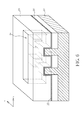
- FIG. 6 is a perspective view illustrating the structure after the trim process is performed.
- the width of the trimmed fin structure 12 may be for example 10 to 30 nm.
- the height of the exposed portion of the fin structure 12 is preferably about one to five times of the width, but not limited thereto.
- a gate dielectric layer (not shown) may be formed on the exposed upper portion of the fin structure 12 . Thereafter, a gate is formed in the trench 24 to cover the channel region of the fin structure 12 .
- the trench 24 may be filled with gate material utilizing for example a CVD process to become a gate material layer 26 further covering a top of the insulation layer 22 .
- the gate material may include for example silicon or metal.
- the later-formed gate material layer 26 will cover the gate dielectric layer.
- the “gate structure” herein may include a gate material layer, or may include a gate dielectric layer and a gate material layer.
- a planarization process such as a CMP process, is performed to planarize the surface of the gate material layer 26 to expose the insulation layer 22 .
- the insulation layer 22 maybe removed through for example an etching process to expose the gate 28 and the portion of the fin structure 12 not covered with the gate 28 . Since the insulation layer 22 may be removed and not remain in the structure, the suitable material is not limited to the material frequently used for interlayer dielectric (for example silicon oxide). Other material can be utilized as soon as it is not harmful to the processes and the structure and the purpose as described above can be attained. The rest of the etch stop layer 20 may be further removed.
- a source and a drain are formed in the fin structure at two sides of the gate 28 .
- a spacer is formed on the sidewall of the gate and the source/drain regions are implanted with dopants through an ion implantation.
- the gate 28 covers the exposed upper portion, including two sidewalls and top, of the fin structure 12 and becomes a tri-gate FET configuration. Furthermore, the gate 28 and the trimmed gate channel are aligned with each other without particular alignment processes. Accordingly, it may be referred to as a self-alignment process.
- the hard mask layer 14 may be removed or allowed to remain.
- a trim process can be also performed on the fin structure 12 as described above. For example, an isotropic etching process may be performed on the trench 24 . Or, a trim process is performed on the hard mask 14 to reduce the width and thereafter the gate channel region is etched to reduce the width.
- FIG. 9 illustrates an embodiment of a FET with a fin structure and a hard mask atop the fin structure after the trim process is performed.
- the thickness of the hard mask layer 14 may be relatively thick, and the gate structure thus formed may have a configuration similar to a tri-gate structure but possess electric properties similar to a double-gate.
- FIG. 10 illustrates an embodiment varied with respect to the embodiment shown in FIG. 9 .
- the gate material layer is planarized to expose the hard mask layer 14 , thereby to form a double-gate FET configuration. It is not necessary for the hard mask 14 to be thick.
- a sacrificial gate is formed as described aforesaid using sacrificial gate material instead of desired gate material. Thereafter, a gate replacement process is performed to replace the sacrificial gate with a desired gate structure.
- the gate structure may include a gate dielectric layer and a gate.
- a sacrificial gate is formed of polysilicon, and thereafter a gate dielectric layer and a metal gate are formed through, for example, a conventional gate replacement process.
- FIG. 11 shows a schematic plan view and FIG. 12 shows a schematic perspective view, both illustrating more in detail a FET with a fin structure according to one aspect of an embodiment of the present invention.
- the channel width W 1 covered with the gate structure 30 is less than the width W 2 of the source/drain region
- the width L 1 of the gate structure 30 is the same as the channel length L 2 of the trimmed gate channel
- two sidewalls 32 and 34 of the gate structure 30 contact two sidewalls 36 and 38 , which face each other, of the two source/drain regions S/D, respectively, without a gap existing between the sidewall 32 and the sidewall 36 or between the sidewall 34 and the sidewall 38 .
- the two sidewalls 32 and 34 of the gate structure 30 are aligned with two edges of the channel region.
- the two edges of the channel region are the two edges opposite to each other in the lengthwise direction of the channel region.
Abstract
Description
Claims (12)
Priority Applications (2)
| Application Number | Priority Date | Filing Date | Title |
|---|---|---|---|
| US13/284,987 US8871575B2 (en) | 2011-10-31 | 2011-10-31 | Method of fabricating field effect transistor with fin structure |
| US14/483,165 US20140374841A1 (en) | 2011-10-31 | 2014-09-11 | Field effect transistor with fin structure |
Applications Claiming Priority (1)
| Application Number | Priority Date | Filing Date | Title |
|---|---|---|---|
| US13/284,987 US8871575B2 (en) | 2011-10-31 | 2011-10-31 | Method of fabricating field effect transistor with fin structure |
Related Child Applications (1)
| Application Number | Title | Priority Date | Filing Date |
|---|---|---|---|
| US14/483,165 Division US20140374841A1 (en) | 2011-10-31 | 2014-09-11 | Field effect transistor with fin structure |
Publications (2)
| Publication Number | Publication Date |
|---|---|
| US20130105867A1 US20130105867A1 (en) | 2013-05-02 |
| US8871575B2 true US8871575B2 (en) | 2014-10-28 |
Family
ID=48171491
Family Applications (2)
| Application Number | Title | Priority Date | Filing Date |
|---|---|---|---|
| US13/284,987 Active 2032-02-06 US8871575B2 (en) | 2011-10-31 | 2011-10-31 | Method of fabricating field effect transistor with fin structure |
| US14/483,165 Abandoned US20140374841A1 (en) | 2011-10-31 | 2014-09-11 | Field effect transistor with fin structure |
Family Applications After (1)
| Application Number | Title | Priority Date | Filing Date |
|---|---|---|---|
| US14/483,165 Abandoned US20140374841A1 (en) | 2011-10-31 | 2014-09-11 | Field effect transistor with fin structure |
Country Status (1)
| Country | Link |
|---|---|
| US (2) | US8871575B2 (en) |
Cited By (2)
| Publication number | Priority date | Publication date | Assignee | Title |
|---|---|---|---|---|
| US20150024584A1 (en) * | 2013-07-17 | 2015-01-22 | Global Foundries, Inc. | Methods for forming integrated circuits with reduced replacement metal gate height variability |
| CN106169500A (en) * | 2015-05-20 | 2016-11-30 | 台湾积体电路制造股份有限公司 | The structure of semiconductor device structure and forming method |
Families Citing this family (23)
| Publication number | Priority date | Publication date | Assignee | Title |
|---|---|---|---|---|
| US8941156B2 (en) * | 2013-01-07 | 2015-01-27 | International Business Machines Corporation | Self-aligned dielectric isolation for FinFET devices |
| US20150118832A1 (en) * | 2013-10-24 | 2015-04-30 | Applied Materials, Inc. | Methods for patterning a hardmask layer for an ion implantation process |
| KR102252224B1 (en) * | 2014-03-24 | 2021-05-14 | 인텔 코포레이션 | Fin sculpting and cladding during replacement gate process for transistor channel applications |
| KR20160134655A (en) * | 2014-03-24 | 2016-11-23 | 인텔 코포레이션 | Techniques for achieving multiple transistor fin dimensions on a single die |
| US9324843B2 (en) | 2014-09-05 | 2016-04-26 | International Business Machines Corporation | High germanium content silicon germanium fins |
| CN111564371B (en) * | 2014-09-09 | 2023-03-24 | 蓝枪半导体有限责任公司 | Fin structure and manufacturing method thereof |
| CN105489494B (en) | 2014-10-09 | 2020-03-31 | 联华电子股份有限公司 | Semiconductor element and manufacturing method thereof |
| US9583625B2 (en) | 2014-10-24 | 2017-02-28 | Globalfoundries Inc. | Fin structures and multi-Vt scheme based on tapered fin and method to form |
| US9496259B2 (en) | 2015-04-14 | 2016-11-15 | Taiwan Semiconductor Manufacturing Co., Ltd. | FinFET semiconductor device having fins with stronger structural strength |
| KR102392695B1 (en) * | 2015-05-26 | 2022-05-02 | 삼성전자주식회사 | A semiconductor device and a method of fabricating the same |
| CN107667430B (en) * | 2015-06-26 | 2022-07-22 | 英特尔公司 | High mobility semiconductor source/drain spacers |
| US9627378B2 (en) * | 2015-06-30 | 2017-04-18 | International Business Machines Corporation | Methods of forming FINFETs with locally thinned channels from fins having in-situ doped epitaxial cladding |
| US10446685B2 (en) | 2015-09-25 | 2019-10-15 | Intel Corporation | High-electron-mobility transistors with heterojunction dopant diffusion barrier |
| WO2017052619A1 (en) | 2015-09-25 | 2017-03-30 | Intel Corporation | High mobility field effect transistors with a retrograded semiconductor source/drain |
| CN108028281B (en) | 2015-09-25 | 2022-04-15 | 英特尔公司 | High mobility field effect transistor with offset semiconductor source/drain pads |
| WO2017052608A1 (en) | 2015-09-25 | 2017-03-30 | Intel Corporation | High-electron-mobility transistors with counter-doped dopant diffusion barrier |
| WO2017171761A1 (en) * | 2016-03-30 | 2017-10-05 | Intel Corporation | Etching fin core to provide fin doubling |
| TWI686850B (en) | 2016-05-19 | 2020-03-01 | 聯華電子股份有限公司 | Semiconductor device and method of fabricating the same |
| WO2017218015A1 (en) | 2016-06-17 | 2017-12-21 | Intel Corporation | High-mobility field effect transistors with wide bandgap fin cladding |
| DE112017007838T5 (en) * | 2017-09-28 | 2020-05-07 | Intel Corporation | TRANSISTORS WITH CHANNEL AND SUB-CHANNEL REGIONS WITH DIFFERENT COMPOSITIONS AND DIMENSIONS |
| CN110783193B (en) * | 2018-07-31 | 2023-06-13 | 中芯国际集成电路制造(上海)有限公司 | Semiconductor structure and forming method thereof |
| US11502163B2 (en) * | 2019-10-23 | 2022-11-15 | Nanya Technology Corporation | Semiconductor structure and fabrication method thereof |
| WO2022016463A1 (en) * | 2020-07-23 | 2022-01-27 | 华为技术有限公司 | Fin field effect transistor and preparation method |
Citations (40)
| Publication number | Priority date | Publication date | Assignee | Title |
|---|---|---|---|---|
| US6043138A (en) | 1996-09-16 | 2000-03-28 | Advanced Micro Devices, Inc. | Multi-step polysilicon deposition process for boron penetration inhibition |
| US6492216B1 (en) | 2002-02-07 | 2002-12-10 | Taiwan Semiconductor Manufacturing Company | Method of forming a transistor with a strained channel |
| US20040195624A1 (en) | 2003-04-04 | 2004-10-07 | National Taiwan University | Strained silicon fin field effect transistor |
| US6855607B2 (en) | 2003-06-12 | 2005-02-15 | Advanced Micro Devices, Inc. | Multi-step chemical mechanical polishing of a gate area in a FinFET |
| US20050051825A1 (en) | 2003-09-09 | 2005-03-10 | Makoto Fujiwara | Semiconductor device and manufacturing method thereof |
| US6921963B2 (en) | 2003-01-23 | 2005-07-26 | Advanced Micro Devices, Inc | Narrow fin FinFET |
| US7013446B2 (en) | 2002-07-05 | 2006-03-14 | Fujitsu Limited | Method, program, and apparatus for designing a semiconductor device |
| US20060099830A1 (en) | 2004-11-05 | 2006-05-11 | Varian Semiconductor Equipment Associates, Inc. | Plasma implantation using halogenated dopant species to limit deposition of surface layers |
| US7087477B2 (en) | 2001-12-04 | 2006-08-08 | International Business Machines Corporation | FinFET SRAM cell using low mobility plane for cell stability and method for forming |
| US7091551B1 (en) | 2005-04-13 | 2006-08-15 | International Business Machines Corporation | Four-bit FinFET NVRAM memory device |
| US7112495B2 (en) | 2003-08-15 | 2006-09-26 | Taiwan Semiconductor Manufacturing Company, Ltd. | Structure and method of a strained channel transistor and a second semiconductor component in an integrated circuit |
| US20060286729A1 (en) | 2005-06-21 | 2006-12-21 | Jack Kavalieros | Complementary metal oxide semiconductor integrated circuit using raised source drain and replacement metal gate |
| US20070015365A1 (en) | 2005-07-14 | 2007-01-18 | Taiwan Semiconductor Manufacturing Co., Ltd. | Method and apparatus for enhanced CMP planarization using surrounded dummy design |
| US20070072376A1 (en) | 2005-09-29 | 2007-03-29 | Semiconductor Manufacturing International (Shanghai) Corporation | Strained-induced mobility enhancement nano-device structure and integrated process architecture for CMOS technologies |
| US20070108528A1 (en) | 2005-11-15 | 2007-05-17 | International Business Machines Corporation | Sram cell |
| US20070158756A1 (en) | 2006-01-12 | 2007-07-12 | Lars Dreeskornfeld | Production method for a FinFET transistor arrangement, and corresponding FinFET transistor arrangement |
| US7247887B2 (en) | 2005-07-01 | 2007-07-24 | Synopsys, Inc. | Segmented channel MOS transistor |
| US7250658B2 (en) | 2003-06-26 | 2007-07-31 | International Business Machines Corporation | Hybrid planar and FinFET CMOS devices |
| US20070218661A1 (en) | 2006-03-15 | 2007-09-20 | Shroff Mehul D | Undoped gate poly integration for improved gate patterning and cobalt silicide extendibility |
| US7309626B2 (en) | 2005-11-15 | 2007-12-18 | International Business Machines Corporation | Quasi self-aligned source/drain FinFET process |
| US20080061366A1 (en) | 2006-09-11 | 2008-03-13 | United Microelectronics Corp. | Complementary metal-oxide-semiconductor device and fabricating method thereof |
| US7352034B2 (en) | 2005-08-25 | 2008-04-01 | International Business Machines Corporation | Semiconductor structures integrating damascene-body FinFET's and planar devices on a common substrate and methods for forming such semiconductor structures |
| US20080157208A1 (en) | 2006-12-29 | 2008-07-03 | Fischer Kevin J | Stressed barrier plug slot contact structure for transistor performance enhancement |
| US7470570B2 (en) | 2006-11-14 | 2008-12-30 | International Business Machines Corporation | Process for fabrication of FinFETs |
| US20090057759A1 (en) | 2007-08-31 | 2009-03-05 | Texas Instruments Incorporated | Mos device and process having low resistance silicide interface using additional source/drain implant |
| US7521324B2 (en) | 2003-04-03 | 2009-04-21 | Tadahiro Ohmi | Semiconductor device and method for manufacturing the same |
| US7531437B2 (en) | 2004-09-30 | 2009-05-12 | Intel Corporation | Method of forming metal gate electrodes using sacrificial gate electrode material and sacrificial gate dielectric material |
| US20090124097A1 (en) | 2007-11-09 | 2009-05-14 | International Business Machines Corporation | Method of forming narrow fins in finfet devices with reduced spacing therebetween |
| US7569857B2 (en) | 2006-09-29 | 2009-08-04 | Intel Corporation | Dual crystal orientation circuit devices on the same substrate |
| US20090200494A1 (en) | 2008-02-11 | 2009-08-13 | Varian Semiconductor Equipment Associates, Inc. | Techniques for cold implantation of carbon-containing species |
| US7592270B2 (en) | 2005-12-15 | 2009-09-22 | Chartered Semiconductor Manufacturing, Ltd. | Modulation of stress in stress film through ion implantation and its application in stress memorization technique |
| US20090242964A1 (en) | 2006-04-26 | 2009-10-01 | Nxp B.V. | Non-volatile memory device |
| US20090269916A1 (en) | 2008-04-28 | 2009-10-29 | Inkuk Kang | Methods for fabricating memory cells having fin structures with semicircular top surfaces and rounded top corners and edges |
| US20100048027A1 (en) | 2008-08-21 | 2010-02-25 | International Business Machines Corporation | Smooth and vertical semiconductor fin structure |
| US20100044783A1 (en) | 2008-08-20 | 2010-02-25 | Taiwan Semiconductor Manufacturing Company, Ltd. | Integrated circuit metal gate structure and method of fabrication |
| US20100072553A1 (en) | 2008-09-23 | 2010-03-25 | Taiwan Semiconductor Manufacturing Co., Ltd. | METAL GATE STRESS FILM FOR MOBILITY ENHANCEMENT IN FinFET DEVICE |
| US20100129994A1 (en) | 2007-02-27 | 2010-05-27 | Yousef Awad | Method for forming a film on a substrate |
| US20100144121A1 (en) | 2008-12-05 | 2010-06-10 | Cheng-Hung Chang | Germanium FinFETs Having Dielectric Punch-Through Stoppers |
| US20100167506A1 (en) | 2008-12-31 | 2010-07-01 | Taiwan Semiconductor Manufacturing Co., Ltd. | Inductive plasma doping |
| US20110121406A1 (en) | 2009-11-20 | 2011-05-26 | Taiwan Semiconductor Manufacturing Company, Ltd. | FinFETs with Different Fin Heights |
Family Cites Families (3)
| Publication number | Priority date | Publication date | Assignee | Title |
|---|---|---|---|---|
| JP4044276B2 (en) * | 2000-09-28 | 2008-02-06 | 株式会社東芝 | Semiconductor device and manufacturing method thereof |
| DE102008030864B4 (en) * | 2008-06-30 | 2010-06-17 | Advanced Micro Devices, Inc., Sunnyvale | Semiconductor device as a double-gate and tri-gate transistor, which are constructed on a solid substrate and method for producing the transistor |
| US8283217B2 (en) * | 2010-03-04 | 2012-10-09 | International Business Machines Corporation | Prevention of oxygen absorption into high-K gate dielectric of silicon-on-insulator based finFET devices |
-
2011
- 2011-10-31 US US13/284,987 patent/US8871575B2/en active Active
-
2014
- 2014-09-11 US US14/483,165 patent/US20140374841A1/en not_active Abandoned
Patent Citations (40)
| Publication number | Priority date | Publication date | Assignee | Title |
|---|---|---|---|---|
| US6043138A (en) | 1996-09-16 | 2000-03-28 | Advanced Micro Devices, Inc. | Multi-step polysilicon deposition process for boron penetration inhibition |
| US7087477B2 (en) | 2001-12-04 | 2006-08-08 | International Business Machines Corporation | FinFET SRAM cell using low mobility plane for cell stability and method for forming |
| US6492216B1 (en) | 2002-02-07 | 2002-12-10 | Taiwan Semiconductor Manufacturing Company | Method of forming a transistor with a strained channel |
| US7013446B2 (en) | 2002-07-05 | 2006-03-14 | Fujitsu Limited | Method, program, and apparatus for designing a semiconductor device |
| US6921963B2 (en) | 2003-01-23 | 2005-07-26 | Advanced Micro Devices, Inc | Narrow fin FinFET |
| US7521324B2 (en) | 2003-04-03 | 2009-04-21 | Tadahiro Ohmi | Semiconductor device and method for manufacturing the same |
| US20040195624A1 (en) | 2003-04-04 | 2004-10-07 | National Taiwan University | Strained silicon fin field effect transistor |
| US6855607B2 (en) | 2003-06-12 | 2005-02-15 | Advanced Micro Devices, Inc. | Multi-step chemical mechanical polishing of a gate area in a FinFET |
| US7250658B2 (en) | 2003-06-26 | 2007-07-31 | International Business Machines Corporation | Hybrid planar and FinFET CMOS devices |
| US7112495B2 (en) | 2003-08-15 | 2006-09-26 | Taiwan Semiconductor Manufacturing Company, Ltd. | Structure and method of a strained channel transistor and a second semiconductor component in an integrated circuit |
| US20050051825A1 (en) | 2003-09-09 | 2005-03-10 | Makoto Fujiwara | Semiconductor device and manufacturing method thereof |
| US7531437B2 (en) | 2004-09-30 | 2009-05-12 | Intel Corporation | Method of forming metal gate electrodes using sacrificial gate electrode material and sacrificial gate dielectric material |
| US20060099830A1 (en) | 2004-11-05 | 2006-05-11 | Varian Semiconductor Equipment Associates, Inc. | Plasma implantation using halogenated dopant species to limit deposition of surface layers |
| US7091551B1 (en) | 2005-04-13 | 2006-08-15 | International Business Machines Corporation | Four-bit FinFET NVRAM memory device |
| US20060286729A1 (en) | 2005-06-21 | 2006-12-21 | Jack Kavalieros | Complementary metal oxide semiconductor integrated circuit using raised source drain and replacement metal gate |
| US7247887B2 (en) | 2005-07-01 | 2007-07-24 | Synopsys, Inc. | Segmented channel MOS transistor |
| US20070015365A1 (en) | 2005-07-14 | 2007-01-18 | Taiwan Semiconductor Manufacturing Co., Ltd. | Method and apparatus for enhanced CMP planarization using surrounded dummy design |
| US7352034B2 (en) | 2005-08-25 | 2008-04-01 | International Business Machines Corporation | Semiconductor structures integrating damascene-body FinFET's and planar devices on a common substrate and methods for forming such semiconductor structures |
| US20070072376A1 (en) | 2005-09-29 | 2007-03-29 | Semiconductor Manufacturing International (Shanghai) Corporation | Strained-induced mobility enhancement nano-device structure and integrated process architecture for CMOS technologies |
| US20070108528A1 (en) | 2005-11-15 | 2007-05-17 | International Business Machines Corporation | Sram cell |
| US7309626B2 (en) | 2005-11-15 | 2007-12-18 | International Business Machines Corporation | Quasi self-aligned source/drain FinFET process |
| US7592270B2 (en) | 2005-12-15 | 2009-09-22 | Chartered Semiconductor Manufacturing, Ltd. | Modulation of stress in stress film through ion implantation and its application in stress memorization technique |
| US20070158756A1 (en) | 2006-01-12 | 2007-07-12 | Lars Dreeskornfeld | Production method for a FinFET transistor arrangement, and corresponding FinFET transistor arrangement |
| US20070218661A1 (en) | 2006-03-15 | 2007-09-20 | Shroff Mehul D | Undoped gate poly integration for improved gate patterning and cobalt silicide extendibility |
| US20090242964A1 (en) | 2006-04-26 | 2009-10-01 | Nxp B.V. | Non-volatile memory device |
| US20080061366A1 (en) | 2006-09-11 | 2008-03-13 | United Microelectronics Corp. | Complementary metal-oxide-semiconductor device and fabricating method thereof |
| US7569857B2 (en) | 2006-09-29 | 2009-08-04 | Intel Corporation | Dual crystal orientation circuit devices on the same substrate |
| US7470570B2 (en) | 2006-11-14 | 2008-12-30 | International Business Machines Corporation | Process for fabrication of FinFETs |
| US20080157208A1 (en) | 2006-12-29 | 2008-07-03 | Fischer Kevin J | Stressed barrier plug slot contact structure for transistor performance enhancement |
| US20100129994A1 (en) | 2007-02-27 | 2010-05-27 | Yousef Awad | Method for forming a film on a substrate |
| US20090057759A1 (en) | 2007-08-31 | 2009-03-05 | Texas Instruments Incorporated | Mos device and process having low resistance silicide interface using additional source/drain implant |
| US20090124097A1 (en) | 2007-11-09 | 2009-05-14 | International Business Machines Corporation | Method of forming narrow fins in finfet devices with reduced spacing therebetween |
| US20090200494A1 (en) | 2008-02-11 | 2009-08-13 | Varian Semiconductor Equipment Associates, Inc. | Techniques for cold implantation of carbon-containing species |
| US20090269916A1 (en) | 2008-04-28 | 2009-10-29 | Inkuk Kang | Methods for fabricating memory cells having fin structures with semicircular top surfaces and rounded top corners and edges |
| US20100044783A1 (en) | 2008-08-20 | 2010-02-25 | Taiwan Semiconductor Manufacturing Company, Ltd. | Integrated circuit metal gate structure and method of fabrication |
| US20100048027A1 (en) | 2008-08-21 | 2010-02-25 | International Business Machines Corporation | Smooth and vertical semiconductor fin structure |
| US20100072553A1 (en) | 2008-09-23 | 2010-03-25 | Taiwan Semiconductor Manufacturing Co., Ltd. | METAL GATE STRESS FILM FOR MOBILITY ENHANCEMENT IN FinFET DEVICE |
| US20100144121A1 (en) | 2008-12-05 | 2010-06-10 | Cheng-Hung Chang | Germanium FinFETs Having Dielectric Punch-Through Stoppers |
| US20100167506A1 (en) | 2008-12-31 | 2010-07-01 | Taiwan Semiconductor Manufacturing Co., Ltd. | Inductive plasma doping |
| US20110121406A1 (en) | 2009-11-20 | 2011-05-26 | Taiwan Semiconductor Manufacturing Company, Ltd. | FinFETs with Different Fin Heights |
Non-Patent Citations (2)
| Title |
|---|
| Daniel Tekleab, S. Samavedam, and P. Zeitzoff, "Modeling and Analysis of Parasitic Resistance in Double-Gate FinFETs," IEEE Transactions on Electron Devices, vol. 56, No. 10, Oct. 2009, pp. 2291-2296, Sep. 23, 2009. |
| Mayank Shrivastava; Ruchit Mehta; Shashank Gupta; Nidhi Agrawal; Maryam Shojaei Baghini; Dinesh Kumar Sharma; Thomas Schulz; Klaus von Arnim; Wolfgang Molzer; Harald Gossner; and V. Ramgopal Rao, "Toward System on Chip (SoC) Development Using FinFET Technology: Challenges, Solutions, Process Co-Development & Optimization Guidelines," IEEE Transactions on Electron Devices, vol. 58, No. 6, Jun. 2011, pp. 1597-1607, Apr. 7, 2011. |
Cited By (4)
| Publication number | Priority date | Publication date | Assignee | Title |
|---|---|---|---|---|
| US20150024584A1 (en) * | 2013-07-17 | 2015-01-22 | Global Foundries, Inc. | Methods for forming integrated circuits with reduced replacement metal gate height variability |
| CN106169500A (en) * | 2015-05-20 | 2016-11-30 | 台湾积体电路制造股份有限公司 | The structure of semiconductor device structure and forming method |
| CN106169500B (en) * | 2015-05-20 | 2019-06-21 | 台湾积体电路制造股份有限公司 | The structure and forming method of semiconductor device structure |
| US10431687B2 (en) | 2015-05-20 | 2019-10-01 | Taiwan Semiconductor Manufacturing Co., Ltd. | Structure and formation method of semiconductor device structure |
Also Published As
| Publication number | Publication date |
|---|---|
| US20140374841A1 (en) | 2014-12-25 |
| US20130105867A1 (en) | 2013-05-02 |
Similar Documents
| Publication | Publication Date | Title |
|---|---|---|
| US8871575B2 (en) | Method of fabricating field effect transistor with fin structure | |
| US11133387B2 (en) | FinFETs having dielectric punch-through stoppers | |
| US9543301B2 (en) | Fin-last FinFET and methods of forming same | |
| US9780200B2 (en) | Semiconductor arrangement for a FinFET and method for manufacturing the same | |
| US7972914B2 (en) | Semiconductor device with FinFET and method of fabricating the same | |
| KR102379701B1 (en) | Semiconductor device having multi-channel and method of forming the same | |
| KR100585178B1 (en) | Semiconductor device comprising finfet having metal gate electrode and fabricating method thereof | |
| US8426283B1 (en) | Method of fabricating a double-gate transistor and a tri-gate transistor on a common substrate | |
| US20060091482A1 (en) | Metal oxide semiconductor (MOS) transistors having a recessed gate electrode and methods of fabricating the same | |
| US9627268B2 (en) | Method for fabricating semiconductor device | |
| US8962430B2 (en) | Method for the formation of a protective dual liner for a shallow trench isolation structure | |
| JP2006522486A (en) | Method for forming a gate in a FinFET device and method for thinning fins in the channel region of the FinFET device | |
| KR20050108916A (en) | Methods of forming a fin field effect transistor using damascene process | |
| CN105810729A (en) | Fin field-effect transistor and manufacturing method thereof | |
| JP2006013303A (en) | Semiconductor device and its manufacturing method | |
| CN112151376B (en) | Semiconductor structure and forming method thereof | |
| CN106409748B (en) | Semiconductor element and manufacturing method thereof | |
| US10811505B2 (en) | Gate electrode having upper and lower capping patterns | |
| WO2014015448A1 (en) | Semiconductor device and manufacturing method thereof | |
| CN111383994B (en) | Semiconductor structure and forming method thereof | |
| TW202101766A (en) | Semiconductor device and method of manufacturing the same | |
| TWI521603B (en) | Method of fabricating field effect transistor with fin structure and field effect transistor with fin structure fabricated therefrom | |
| CN111276442B (en) | Semiconductor structure and forming method thereof | |
| CN115602717A (en) | Semiconductor structure and forming method thereof | |
| TWI514480B (en) | Method for manufacturing multi-gate transistor device |
Legal Events
| Date | Code | Title | Description |
|---|---|---|---|
| AS | Assignment |
Owner name: UNITED MICROELECTRONICS CORP., TAIWAN Free format text: ASSIGNMENT OF ASSIGNORS INTEREST;ASSIGNORS:WANG, CHIH-JUNG;CHEN, TONG-YU;REEL/FRAME:027144/0509 Effective date: 20111024 |
|
| STCF | Information on status: patent grant |
Free format text: PATENTED CASE |
|
| MAFP | Maintenance fee payment |
Free format text: PAYMENT OF MAINTENANCE FEE, 4TH YEAR, LARGE ENTITY (ORIGINAL EVENT CODE: M1551) Year of fee payment: 4 |
|
| MAFP | Maintenance fee payment |
Free format text: PAYMENT OF MAINTENANCE FEE, 8TH YEAR, LARGE ENTITY (ORIGINAL EVENT CODE: M1552); ENTITY STATUS OF PATENT OWNER: LARGE ENTITY Year of fee payment: 8 |