US8854224B2 - Conveying device information relating to wireless charging - Google Patents
Conveying device information relating to wireless charging Download PDFInfo
- Publication number
- US8854224B2 US8854224B2 US12/572,371 US57237109A US8854224B2 US 8854224 B2 US8854224 B2 US 8854224B2 US 57237109 A US57237109 A US 57237109A US 8854224 B2 US8854224 B2 US 8854224B2
- Authority
- US
- United States
- Prior art keywords
- electronic device
- charging
- power
- wireless charger
- display
- Prior art date
- Legal status (The legal status is an assumption and is not a legal conclusion. Google has not performed a legal analysis and makes no representation as to the accuracy of the status listed.)
- Active, expires
Links
- 238000000034 method Methods 0.000 claims description 31
- 238000001514 detection method Methods 0.000 claims description 5
- 230000008569 process Effects 0.000 claims description 3
- 230000008878 coupling Effects 0.000 description 39
- 238000010168 coupling process Methods 0.000 description 39
- 238000005859 coupling reaction Methods 0.000 description 39
- 239000003990 capacitor Substances 0.000 description 16
- 230000011664 signaling Effects 0.000 description 15
- 230000002441 reversible effect Effects 0.000 description 12
- 238000010586 diagram Methods 0.000 description 11
- 238000012546 transfer Methods 0.000 description 11
- 238000004891 communication Methods 0.000 description 8
- 230000000670 limiting effect Effects 0.000 description 7
- 230000005855 radiation Effects 0.000 description 7
- 230000008859 change Effects 0.000 description 6
- 238000006243 chemical reaction Methods 0.000 description 5
- 230000005540 biological transmission Effects 0.000 description 4
- 230000001413 cellular effect Effects 0.000 description 3
- 238000005516 engineering process Methods 0.000 description 3
- 230000006870 function Effects 0.000 description 3
- 230000007246 mechanism Effects 0.000 description 3
- 230000003287 optical effect Effects 0.000 description 3
- 230000005672 electromagnetic field Effects 0.000 description 2
- 239000000835 fiber Substances 0.000 description 2
- 239000002245 particle Substances 0.000 description 2
- 230000001902 propagating effect Effects 0.000 description 2
- 230000002829 reductive effect Effects 0.000 description 2
- 238000004804 winding Methods 0.000 description 2
- 230000003044 adaptive effect Effects 0.000 description 1
- 230000003321 amplification Effects 0.000 description 1
- 238000013459 approach Methods 0.000 description 1
- 238000004590 computer program Methods 0.000 description 1
- 239000004020 conductor Substances 0.000 description 1
- 230000007423 decrease Effects 0.000 description 1
- 238000013461 design Methods 0.000 description 1
- 230000005684 electric field Effects 0.000 description 1
- 230000002708 enhancing effect Effects 0.000 description 1
- 230000001939 inductive effect Effects 0.000 description 1
- 239000002184 metal Substances 0.000 description 1
- 238000012986 modification Methods 0.000 description 1
- 230000004048 modification Effects 0.000 description 1
- 230000005404 monopole Effects 0.000 description 1
- 238000003199 nucleic acid amplification method Methods 0.000 description 1
- 230000036961 partial effect Effects 0.000 description 1
- 230000000135 prohibitive effect Effects 0.000 description 1
- 230000000644 propagated effect Effects 0.000 description 1
- 230000004044 response Effects 0.000 description 1
- 238000012795 verification Methods 0.000 description 1
- 229910000859 α-Fe Inorganic materials 0.000 description 1
Images


Classifications
-
- H02J7/025—
-
- H—ELECTRICITY
- H02—GENERATION; CONVERSION OR DISTRIBUTION OF ELECTRIC POWER
- H02J—CIRCUIT ARRANGEMENTS OR SYSTEMS FOR SUPPLYING OR DISTRIBUTING ELECTRIC POWER; SYSTEMS FOR STORING ELECTRIC ENERGY
- H02J7/00—Circuit arrangements for charging or depolarising batteries or for supplying loads from batteries
- H02J7/0042—Circuit arrangements for charging or depolarising batteries or for supplying loads from batteries characterised by the mechanical construction
- H02J7/0044—Circuit arrangements for charging or depolarising batteries or for supplying loads from batteries characterised by the mechanical construction specially adapted for holding portable devices containing batteries
-
- H—ELECTRICITY
- H02—GENERATION; CONVERSION OR DISTRIBUTION OF ELECTRIC POWER
- H02J—CIRCUIT ARRANGEMENTS OR SYSTEMS FOR SUPPLYING OR DISTRIBUTING ELECTRIC POWER; SYSTEMS FOR STORING ELECTRIC ENERGY
- H02J50/00—Circuit arrangements or systems for wireless supply or distribution of electric power
- H02J50/10—Circuit arrangements or systems for wireless supply or distribution of electric power using inductive coupling
- H02J50/12—Circuit arrangements or systems for wireless supply or distribution of electric power using inductive coupling of the resonant type
-
- H—ELECTRICITY
- H02—GENERATION; CONVERSION OR DISTRIBUTION OF ELECTRIC POWER
- H02J—CIRCUIT ARRANGEMENTS OR SYSTEMS FOR SUPPLYING OR DISTRIBUTING ELECTRIC POWER; SYSTEMS FOR STORING ELECTRIC ENERGY
- H02J50/00—Circuit arrangements or systems for wireless supply or distribution of electric power
- H02J50/20—Circuit arrangements or systems for wireless supply or distribution of electric power using microwaves or radio frequency waves
-
- H—ELECTRICITY
- H02—GENERATION; CONVERSION OR DISTRIBUTION OF ELECTRIC POWER
- H02J—CIRCUIT ARRANGEMENTS OR SYSTEMS FOR SUPPLYING OR DISTRIBUTING ELECTRIC POWER; SYSTEMS FOR STORING ELECTRIC ENERGY
- H02J50/00—Circuit arrangements or systems for wireless supply or distribution of electric power
- H02J50/80—Circuit arrangements or systems for wireless supply or distribution of electric power involving the exchange of data, concerning supply or distribution of electric power, between transmitting devices and receiving devices
-
- H—ELECTRICITY
- H02—GENERATION; CONVERSION OR DISTRIBUTION OF ELECTRIC POWER
- H02J—CIRCUIT ARRANGEMENTS OR SYSTEMS FOR SUPPLYING OR DISTRIBUTING ELECTRIC POWER; SYSTEMS FOR STORING ELECTRIC ENERGY
- H02J50/00—Circuit arrangements or systems for wireless supply or distribution of electric power
- H02J50/90—Circuit arrangements or systems for wireless supply or distribution of electric power involving detection or optimisation of position, e.g. alignment
-
- H—ELECTRICITY
- H02—GENERATION; CONVERSION OR DISTRIBUTION OF ELECTRIC POWER
- H02J—CIRCUIT ARRANGEMENTS OR SYSTEMS FOR SUPPLYING OR DISTRIBUTING ELECTRIC POWER; SYSTEMS FOR STORING ELECTRIC ENERGY
- H02J7/00—Circuit arrangements for charging or depolarising batteries or for supplying loads from batteries
- H02J7/0047—Circuit arrangements for charging or depolarising batteries or for supplying loads from batteries with monitoring or indicating devices or circuits
- H02J7/0048—Detection of remaining charge capacity or state of charge [SOC]
-
- H—ELECTRICITY
- H02—GENERATION; CONVERSION OR DISTRIBUTION OF ELECTRIC POWER
- H02J—CIRCUIT ARRANGEMENTS OR SYSTEMS FOR SUPPLYING OR DISTRIBUTING ELECTRIC POWER; SYSTEMS FOR STORING ELECTRIC ENERGY
- H02J7/00—Circuit arrangements for charging or depolarising batteries or for supplying loads from batteries
- H02J7/0013—Circuit arrangements for charging or depolarising batteries or for supplying loads from batteries acting upon several batteries simultaneously or sequentially
-
- H—ELECTRICITY
- H02—GENERATION; CONVERSION OR DISTRIBUTION OF ELECTRIC POWER
- H02J—CIRCUIT ARRANGEMENTS OR SYSTEMS FOR SUPPLYING OR DISTRIBUTING ELECTRIC POWER; SYSTEMS FOR STORING ELECTRIC ENERGY
- H02J7/00—Circuit arrangements for charging or depolarising batteries or for supplying loads from batteries
- H02J7/0047—Circuit arrangements for charging or depolarising batteries or for supplying loads from batteries with monitoring or indicating devices or circuits
- H02J7/0048—Detection of remaining charge capacity or state of charge [SOC]
- H02J7/0049—Detection of fully charged condition
Definitions
- the present invention relates generally to wireless charging, and more specifically to devices, systems, and methods related to wireless chargers.
- an electronic device may be connected to a power source, via a cord and, therefore, a charging status of the electronic device may be quickly and easily established.
- a charging status of an electronic device may not be known. For example, it may not be evident that an electronic device is actually receiving power or how much power is stored within the electronic device.
- FIG. 1 shows a simplified block diagram of a wireless power transfer system.
- FIG. 2 shows a simplified schematic diagram of a wireless power transfer system.
- FIG. 3 shows a schematic diagram of a loop antenna for use in exemplary embodiments of the present invention.
- FIGS. 4A and 4B show layouts of loop antennas for transmit and receive antennas according to exemplary embodiments of the present invention.
- FIG. 5 shows various placement points for a receive antenna relative to a transmit antenna to illustrate coupling strengths in coplanar and coaxial placements.
- FIG. 6 is a simplified block diagram of a transmitter, in accordance with an exemplary embodiment of the present invention.
- FIG. 7 is a simplified block diagram of a receiver, in accordance with an exemplary embodiment of the present invention.
- FIG. 8 shows a simplified schematic of a portion of transmit circuitry for carrying out messaging between a transmitter and a receiver.
- FIGS. 9A-9C shows a simplified schematic of a portion of receive circuitry in various states to illustrate messaging between a receiver and a transmitter.
- FIGS. 10A-10C shows a simplified schematic of a portion of alternative receive circuitry in various states to illustrate messaging between a receiver and a transmitter.
- FIGS. 11A-11D are simplified block diagrams illustrating a beacon power mode for transmitting power between a transmitter and a receiver.
- FIG. 12A illustrates a large transmit antenna with a three different smaller repeater antennas disposed coplanar with, and within a perimeter of, the transmit antenna.
- FIG. 12B illustrates a large transmit antenna with smaller repeater antennas with offset coaxial placements and offset coplanar placements relative to the transmit antenna.
- FIG. 13 illustrates a charging device including an interface having at least one indicator display, according to an exemplary embodiment of the present invention.
- FIG. 14 illustrates a charging system including a charging device and at least one chargeable electronic device, in accordance with an exemplary embodiment of the present invention.
- FIG. 15 illustrates a charging device including an interface having an indicator display, according to an exemplary embodiment of the present invention.
- FIG. 16 illustrates another charging device including an interface having at least one indicator display, in accordance with an exemplary embodiment of the present invention.
- FIG. 17 illustrates a charging device including an internal region and an interface, according to an exemplary embodiment of the present invention.
- FIG. 18 illustrates an electronic device including a display element, according to an exemplary embodiment of the present invention.
- FIG. 19 is a flowchart illustrating a method of operating a charging device, in accordance with an exemplary embodiment of the present invention.
- FIG. 20 is a flowchart illustrating another method of operating a charging device, in accordance with an exemplary embodiment of the present invention.
- wireless power is used herein to mean any form of energy associated with electric fields, magnetic fields, electromagnetic fields, or otherwise that is transmitted between from a transmitter to a receiver without the use of physical electromagnetic conductors.
- FIG. 1 illustrates wireless transmission or charging system 100 , in accordance with various exemplary embodiments of the present invention.
- Input power 102 is provided to a transmitter 104 for generating a radiated field 106 for providing energy transfer.
- a receiver 108 couples to the radiated field 106 and generates an output power 110 for storing or consumption by a device (not shown) coupled to the output power 110 .
- Both the transmitter 104 and the receiver 108 are separated by a distance 112 .
- transmitter 104 and receiver 108 are configured according to a mutual resonant relationship and when the resonant frequency of receiver 108 and the resonant frequency of transmitter 104 are exactly identical, transmission losses between the transmitter 104 and the receiver 108 are minimal when the receiver 108 is located in the “near-field” of the radiated field 106 .
- Transmitter 104 further includes a transmit antenna 114 for providing a means for energy transmission and receiver 108 further includes a receive antenna 118 for providing a means for energy reception.
- the transmit and receive antennas are sized according to applications and devices to be associated therewith. As stated, an efficient energy transfer occurs by coupling a large portion of the energy in the near-field of the transmitting antenna to a receiving antenna rather than propagating most of the energy in an electromagnetic wave to the far-field. When in this near-field a coupling mode may be developed between the transmit antenna 114 and the receive antenna 118 .
- the area around the antennas 114 and 118 where this near-field coupling may occur is referred to herein as a coupling-mode region.
- FIG. 2 shows a simplified schematic diagram of a wireless power transfer system.
- the transmitter 104 includes an oscillator 122 , a power amplifier 124 and a filter and matching circuit 126 .
- the oscillator is configured to generate at a desired frequency, which may be adjusted in response to adjustment signal 123 .
- the oscillator signal may be amplified by the power amplifier 124 with an amplification amount responsive to control signal 125 .
- the filter and matching circuit 126 may be included to filter out harmonics or other unwanted frequencies and match the impedance of the transmitter 104 to the transmit antenna 114 .
- the receiver may include a matching circuit 132 and a rectifier and switching circuit to generate a DC power output to charge a battery 136 as shown in FIG. 2 or power a device coupled to the receiver (not shown).
- the matching circuit 132 may be included to match the impedance of the receiver 108 to the receive antenna 118 .
- antennas used in exemplary embodiments may be configured as a “loop” antenna 150 , which may also be referred to herein as a “magnetic” antenna.
- Loop antennas may be configured to include an air core or a physical core such as a ferrite core. Air core loop antennas may be more tolerable to extraneous physical devices placed in the vicinity of the core. Furthermore, an air core loop antenna allows the placement of other components within the core area. In addition, an air core loop may more readily enable placement of the receive antenna 118 ( FIG. 2 ) within a plane of the transmit antenna 114 ( FIG. 2 ) where the coupled-mode region of the transmit antenna 114 ( FIG. 2 ) may be more powerful.
- the resonant frequency of the loop or magnetic antennas is based on the inductance and capacitance.
- Inductance in a loop antenna is generally simply the inductance created by the loop, whereas, capacitance is generally added to the loop antenna's inductance to create a resonant structure at a desired resonant frequency.
- capacitor 152 and capacitor 154 may be added to the antenna to create a resonant circuit that generates resonant signal 156 . Accordingly, for larger diameter loop antennas, the size of capacitance needed to induce resonance decreases as the diameter or inductance of the loop increases. Furthermore, as the diameter of the loop or magnetic antenna increases, the efficient energy transfer area of the near-field increases.
- resonant circuits are possible.
- a capacitor may be placed in parallel between the two terminals of the loop antenna.
- the resonant signal 156 may be an input to the loop antenna 150 .
- Exemplary embodiments of the invention include coupling power between two antennas that are in the near-fields of each other.
- the near-field is an area around the antenna in which electromagnetic fields exist but may not propagate or radiate away from the antenna. They are typically confined to a volume that is near the physical volume of the antenna.
- magnetic type antennas such as single and multi-turn loop antennas are used for both transmit (Tx) and receive (Rx) antenna systems since magnetic near-field amplitudes tend to be higher for magnetic type antennas in comparison to the electric near-fields of an electric-type antenna (e.g., a small dipole). This allows for potentially higher coupling between the pair.
- “electric” antennas e.g., dipoles and monopoles
- a combination of magnetic and electric antennas is also contemplated.
- the Tx antenna can be operated at a frequency that is low enough and with an antenna size that is large enough to achieve good coupling (e.g., > ⁇ 4 dB) to a small Rx antenna at significantly larger distances than allowed by far-field and inductive approaches mentioned earlier. If the Tx antenna is sized correctly, high coupling levels (e.g., ⁇ 2 to ⁇ 4 dB) can be achieved when the Rx antenna on a host device is placed within a coupling-mode region (i.e., in the near-field) of the driven Tx loop antenna.
- a coupling-mode region i.e., in the near-field
- FIGS. 4A and 4B show layouts of loop antennas for transmit and receive antennas according to exemplary embodiments of the present invention.
- Loop antennas may be configured in a number of different ways, with single loops or multiple loops at wide variety of sizes.
- the loops may be a number of different shapes, such as, for example only, circular, elliptical, square, and rectangular.
- FIG. 4A illustrates a large square loop transmit antenna 114 S and a small square loop receive antenna 118 placed in the same plane as the transmit antenna 114 S and near the center of the transmit antenna 114 S.
- FIG. 4A illustrates a large square loop transmit antenna 114 S and a small square loop receive antenna 118 placed in the same plane as the transmit antenna 114 S and near the center of the transmit antenna 114 S.
- FIG. 4B illustrates a large circular loop transmit antenna 114 C and a small square loop receive antenna 118 ′ placed in the same plane as the transmit antenna 114 C and near the center of the transmit antenna 114 C.
- the square loop transmit antenna 114 S has side lengths of “a” while the circular loop transmit antenna 114 C has a diameter of “ ⁇ .”
- ⁇ eq 4a/ ⁇ .
- FIG. 5 shows various placement points for a receive antenna relative to a transmit antenna to illustrate coupling strengths in coplanar and coaxial placements.
- “Coplanar,” as used herein, means that the transmit antenna and receive antenna have planes that are substantially aligned (i.e., have surface normals pointing in substantially the same direction) and with no distance (or a small distance) between the planes of the transmit antenna and the receive antenna.
- “Coaxial,” as used herein, means that the transmit antenna and receive antenna have planes that are substantially aligned (i.e., have surface normals pointing in substantially the same direction) and the distance between the two planes is not trivial and furthermore, the surface normal of the transmit antenna and the receive antenna lie substantially along the same vector, or the two normals are in echelon.
- points p 1 , p 2 , p 3 , and p 7 are all coplanar placement points for a receive antenna relative to a transmit antenna.
- point p 5 and p 6 are coaxial placement points for a receive antenna relative to a transmit antenna.
- the table below shows coupling strength (S 21 ) and coupling efficiency (expressed as a percentage of power transmitted from the transmit antenna that reached the receive antenna) at the various placement points (p 1 -p 7 ) illustrated in FIG. 5 .
- the coplanar placement points p 1 , p 2 , and p 3 all show relatively high coupling efficiencies.
- Placement point p 7 is also a coplanar placement point, but is outside of the transmit loop antenna. While placement point p 7 does not have a high coupling efficiency, it is clear that there is some coupling and the coupling-mode region extends beyond the perimeter of the transmit loop antenna.
- Placement point p 5 is coaxial with the transmit antenna and shows substantial coupling efficiency.
- the coupling efficiency for placement point p 5 is not as high as the coupling efficiencies for the coplanar placement points. However, the coupling efficiency for placement point p 5 is high enough that substantial power can be conveyed between the transmit antenna and a receive antenna in a coaxial placement.
- Placement point p 4 is within the circumference of the transmit antenna but at a slight distance above the plane of the transmit antenna in a position that may be referred to as an offset coaxial placement (i.e., with surface normals in substantially the same direction but at different locations) or offset coplanar (i.e., with surface normals in substantially the same direction but with planes that are offset relative to each other). From the table it can be seen that with an offset distance of 2.5 cm, placement point p 4 still has relatively good coupling efficiency.
- Placement point p 6 illustrates a placement point outside the circumference of the transmit antenna and at a substantial distance above the plane of the transmit antenna. As can be seen from the table, placement point p 7 shows little coupling efficiency between the transmit and receive antennas.
- FIG. 6 is a simplified block diagram of a transmitter, in accordance with an exemplary embodiment of the present invention.
- a transmitter 200 includes transmit circuitry 202 and a transmit antenna 204 .
- transmit circuitry 202 provides RF power to the transmit antenna 204 by providing an oscillating signal resulting in generation of near-field energy about the transmit antenna 204 .
- transmitter 200 may operate at the 13.56 MHz ISM band.
- Exemplary transmit circuitry 202 includes a fixed impedance matching circuit 206 for matching the impedance of the transmit circuitry 202 (e.g., 50 ohms) to the transmit antenna 204 and a low pass filter (LPF) 208 configured to reduce harmonic emissions to levels to prevent self-jamming of devices coupled to receivers 108 ( FIG. 1 ).
- Other exemplary embodiments may include different filter topologies, including but not limited to, notch filters that attenuate specific frequencies while passing others and may include an adaptive impedance match, that can be varied based on measurable transmit metrics, such as output power to the antenna or DC current draw by the power amplifier.
- Transmit circuitry 202 further includes a power amplifier 210 configured to drive an RF signal as determined by an oscillator 212 .
- the transmit circuitry may be comprised of discrete devices or circuits, or alternately, may be comprised of an integrated assembly.
- An exemplary RF power output from transmit antenna 204 may be on the order of 2.5 Watts.
- Transmit circuitry 202 further includes a processor 214 for enabling the oscillator 212 during transmit phases (or duty cycles) for specific receivers, for adjusting the frequency of the oscillator, and for adjusting the output power level for implementing a communication protocol for interacting with neighboring devices through their attached receivers.
- the transmit circuitry 202 may further include a load sensing circuit 216 for detecting the presence or absence of active receivers in the vicinity of the near-field generated by transmit antenna 204 .
- a load sensing circuit 216 monitors the current flowing to the power amplifier 210 , which is affected by the presence or absence of active receivers in the vicinity of the near-field generated by transmit antenna 204 . Detection of changes to the loading on the power amplifier 210 are monitored by processor 214 for use in determining whether to enable the oscillator 212 for transmitting energy to communicate with an active receiver.
- Transmit antenna 204 may be implemented as an antenna strip with the thickness, width and metal type selected to keep resistive losses low.
- the transmit antenna 204 can generally be configured for association with a larger structure such as a table, mat, lamp or other less portable configuration. Accordingly, the transmit antenna 204 generally will not need “turns” in order to be of a practical dimension.
- An exemplary implementation of a transmit antenna 204 may be “electrically small” (i.e., fraction of the wavelength) and tuned to resonate at lower usable frequencies by using capacitors to define the resonant frequency.
- the transmit antenna 204 may be larger in diameter, or length of side if a square loop, (e.g., 0.50 meters) relative to the receive antenna, the transmit antenna 204 will not necessarily need a large number of turns to obtain a reasonable capacitance.
- FIG. 7 is a block diagram of a receiver, in accordance with an exemplary embodiment of the present invention.
- a receiver 300 includes receive circuitry 302 and a receive antenna 304 . Receiver 300 further couples to device 350 for providing received power thereto. It should be noted that receiver 300 is illustrated as being external to device 350 but may be integrated into device 350 . Generally, energy is propagated wirelessly to receive antenna 304 and then coupled through receive circuitry 302 to device 350 .
- Receive antenna 304 is tuned to resonate at the same frequency, or near the same frequency, as transmit antenna 204 ( FIG. 6 ). Receive antenna 304 may be similarly dimensioned with transmit antenna 204 or may be differently sized based upon the dimensions of an associated device 350 .
- device 350 may be a portable electronic device having diametric or length dimension smaller that the diameter of length of transmit antenna 204 .
- receive antenna 304 may be implemented as a multi-turn antenna in order to reduce the capacitance value of a tuning capacitor (not shown) and increase the receive antenna's impedance.
- receive antenna 304 may be placed around the substantial circumference of device 350 in order to maximize the antenna diameter and reduce the number of loop turns (i.e., windings) of the receive antenna and the inter-winding capacitance.
- Receive circuitry 302 provides an impedance match to the receive antenna 304 .
- Receive circuitry 302 includes power conversion circuitry 306 for converting a received RF energy source into charging power for use by device 350 .
- Power conversion circuitry 306 includes an RF-to-DC converter 308 and may also in include a DC-to-DC converter 310 .
- RF-to-DC converter 308 rectifies the RF energy signal received at receive antenna 304 into a non-alternating power while DC-to-DC converter 310 converts the rectified RF energy signal into an energy potential (e.g., voltage) that is compatible with device 350 .
- Various RF-to-DC converters are contemplated including partial and full rectifiers, regulators, bridges, doublers, as well as linear and switching converters.
- Receive circuitry 302 may further include switching circuitry 312 for connecting receive antenna 304 to the power conversion circuitry 306 or alternatively for disconnecting the power conversion circuitry 306 . Disconnecting receive antenna 304 from power conversion circuitry 306 not only suspends charging of device 350 , but also changes the “load” as “seen” by the transmitter 200 ( FIG. 2 ) as is explained more fully below.
- transmitter 200 includes load sensing circuit 216 which detects fluctuations in the bias current provided to transmitter power amplifier 210 . Accordingly, transmitter 200 has a mechanism for determining when receivers are present in the transmitter's near-field.
- a receiver When multiple receivers 300 are present in a transmitter's near-field, it may be desirable to time-multiplex the loading and unloading of one or more receivers to enable other receivers to more efficiently couple to the transmitter.
- a receiver may also be cloaked in order to eliminate coupling to other nearby receivers or to reduce loading on nearby transmitters.
- This “unloading” of a receiver is also known herein as a “cloaking”
- this switching between unloading and loading controlled by receiver 300 and detected by transmitter 200 provides a communication mechanism from receiver 300 to transmitter 200 as is explained more fully below.
- a protocol can be associated with the switching which enables the sending of a message from receiver 300 to transmitter 200 .
- a switching speed may be on the order of 100 ⁇ sec.
- communication between the transmitter and the receiver refers to a device sensing and charging control mechanism, rather than conventional two-way communication.
- the transmitter uses on/off keying of the transmitted signal to adjust whether energy is available in the near-filed.
- the receivers interpret these changes in energy as a message from the transmitter.
- the receiver uses tuning and de-tuning of the receive antenna to adjust how much power is being accepted from the near-field.
- the transmitter can detect this difference in power used from the near-field and interpret these changes as a message from the receiver.
- Receive circuitry 302 may further include signaling detector and beacon circuitry 314 used to identify received energy fluctuations, which may correspond to informational signaling from the transmitter to the receiver. Furthermore, signaling and beacon circuitry 314 may also be used to detect the transmission of a reduced RF signal energy (i.e., a beacon signal) and to rectify the reduced RF signal energy into a nominal power for awakening either un-powered or power-depleted circuits within receive circuitry 302 in order to configure receive circuitry 302 for wireless charging.
- signaling detector and beacon circuitry 314 used to identify received energy fluctuations, which may correspond to informational signaling from the transmitter to the receiver. Furthermore, signaling and beacon circuitry 314 may also be used to detect the transmission of a reduced RF signal energy (i.e., a beacon signal) and to rectify the reduced RF signal energy into a nominal power for awakening either un-powered or power-depleted circuits within receive circuitry 302 in order to configure receive circuitry 302 for wireless charging.
- a reduced RF signal energy i.
- Receive circuitry 302 further includes processor 316 for coordinating the processes of receiver 300 described herein including the control of switching circuitry 312 described herein. Cloaking of receiver 300 may also occur upon the occurrence of other events including detection of an external wired charging source (e.g., wall/USB power) providing charging power to device 350 .
- Processor 316 in addition to controlling the cloaking of the receiver, may also monitor beacon circuitry 314 to determine a beacon state and extract messages sent from the transmitter. Processor 316 may also adjust DC-to-DC converter 310 for improved performance.
- FIG. 8 shows a simplified schematic of a portion of transmit circuitry for carrying out messaging between a transmitter and a receiver.
- a means for communication may be enabled between the transmitter and the receiver.
- a power amplifier 210 drives the transmit antenna 204 to generate the radiated field.
- the power amplifier is driven by a carrier signal 220 that is oscillating at a desired frequency for the transmit antenna 204 .
- a transmit modulation signal 224 is used to control the output of the power amplifier 210 .
- the transmit circuitry can send signals to receivers by using an ON/OFF keying process on the power amplifier 210 .
- the transmit modulation signal 224 when the transmit modulation signal 224 is asserted, the power amplifier 210 will drive the frequency of the carrier signal 220 out on the transmit antenna 204 .
- the transmit modulation signal 224 When the transmit modulation signal 224 is negated, the power amplifier will not drive out any frequency on the transmit antenna 204 .
- the transmit circuitry of FIG. 8 also includes a load sensing circuit 216 that supplies power to the power amplifier 210 and generates a receive signal 235 output.
- a voltage drop across resistor R s develops between the power in signal 226 and the power supply 228 to the power amplifier 210 . Any change in the power consumed by the power amplifier 210 will cause a change in the voltage drop that will be amplified by differential amplifier 230 .
- the transmit antenna is in coupled mode with a receive antenna in a receiver (not shown in FIG. 8 ) the amount of current drawn by the power amplifier 210 will change. In other words, if no coupled mode resonance exist for the transmit antenna 210 , the power required to drive the radiated field will be first amount.
- the receive signal 235 can indicate the presence of a receive antenna coupled to the transmit antenna 235 and can also detect signals sent from the receive antenna, as explained below. Additionally, a change in receiver current draw will be observable in the transmitter's power amplifier current draw, and this change can be used to detect signals from the receive antennas, as explained below.
- FIGS. 9A-9C show a simplified schematic of a portion of receive circuitry in various states to illustrate messaging between a receiver and a transmitter. All of FIGS. 9A-9C show the same circuit elements with the difference being state of the various switches.
- a receive antenna 304 includes a characteristic inductance L 1 , which drives node 350 .
- Node 350 is selectively coupled to ground through switch S 1 A.
- Node 350 is also selectively coupled to diode D 1 and rectifier 318 through switch SIB.
- the rectifier 318 supplies a DC power signal 322 to a receive device (not shown) to power the receive device, charge a battery, or a combination thereof.
- the diode D 1 is coupled to a transmit signal 320 which is filtered to remove harmonics and unwanted frequencies with capacitor C 3 and resistor R 1 .
- the combination of D 1 , C 3 , and R 1 can generate a signal on the transmit signal 320 that mimics the transmit modulation generated by the transmit modulation signal 224 discussed above with reference to the transmitter in FIG. 8 .
- Exemplary embodiments of the invention includes modulation of the receive device's current draw and modulation of the receive antenna's impedance to accomplish reverse link signaling.
- the load sensing circuit 216 detects the resulting power changes on the transmit antenna and from these changes can generate the receive signal 235 .
- the current draw through the transmitter can be changed by modifying the state of switches S 1 A and S 2 A.
- switch S 1 A and switch S 2 A are both open creating a “DC open state” and essentially removing the load from the transmit antenna 204 . This reduces the current seen by the transmitter.
- switch S 1 A is closed and switch S 2 A is open creating a “DC short state” for the receive antenna 304 .
- the state in FIG. 9B can be used to increase the current seen in the transmitter.
- switch S 1 A is open and switch S 2 A is closed creating a normal receive mode (also referred to herein as a “DC operating state”) wherein power can be supplied by the DC out signal 322 and a transmit signal 320 can be detected.
- a normal receive mode also referred to herein as a “DC operating state”
- the receiver receives a normal amount of power, thus consuming more or less power from the transmit antenna than the DC open state or the DC short state.
- Reverse link signaling may be accomplished by switching between the DC operating state ( FIG. 9C ) and the DC short state ( FIG. 9B ). Reverse link signaling also may be accomplished by switching between the DC operating state ( FIG. 9C ) and the DC open state ( FIG. 9A ).
- FIGS. 10A-10C shows a simplified schematic of a portion of alternative receive circuitry in various states to illustrate messaging between a receiver and a transmitter. All of FIGS. 10A-10C show the same circuit elements with the difference being state of the various switches.
- a receive antenna 304 includes a characteristic inductance L 1 , which drives node 350 .
- Node 350 is selectively coupled to ground through capacitor C 1 and switch S 1 B.
- Node 350 is also AC coupled to diode D 1 and rectifier 318 through capacitor C 2 .
- the diode D 1 is coupled to a transmit signal 320 which is filtered to remove harmonics and unwanted frequencies with capacitor C 3 and resistor R 1 .
- the combination of D 1 , C 3 , and R 1 can generate a signal on the transmit signal 320 that mimics the transmit modulation generated by the transmit modulation signal 224 discussed above with reference to the transmitter in FIG. 8 .
- the rectifier 318 is connected to switch S 2 B, which is connected in series with resistor R 2 and ground.
- the rectifier 318 also is connected to switch S 3 B.
- the other side of switch S 3 B supplies a DC power signal 322 to a receive device (not shown) to power the receive device, charge a battery, or a combination thereof.
- the DC impedance of the receive antenna 304 is changed by selectively coupling the receive antenna to ground through switch SIB.
- the impedance of the antenna can be modified to generate the reverse link signaling by modifying the state of switches S 1 B, S 2 B, and S 3 B to change the AC impedance of the receive antenna 304 .
- the resonant frequency of the receive antenna 304 may be tuned with capacitor C 2 .
- the AC impedance of the receive antenna 304 may be changed by selectively coupling the receive antenna 304 through capacitor C 1 using switch S 1 B, essentially changing the resonance circuit to a different frequency that will be outside of a range that will optimally couple with the transmit antenna. If the resonance frequency of the receive antenna 304 is near the resonant frequency of the transmit antenna, and the receive antenna 304 is in the near-field of the transmit antenna, a coupling mode may develop wherein the receiver can draw significant power from the radiated field 106 .
- switch S 1 B is closed, which de-tunes the antenna and creates an “AC cloaking state,” essentially “cloaking” the receive antenna 304 from detection by the transmit antenna 204 because the receive antenna does not resonate at the transmit antenna's frequency. Since the receive antenna will not be in a coupled mode, the state of switches S 2 B and S 3 B are not particularly important to the present discussion.
- switch S 1 B is open, switch S 2 B is closed, and switch S 3 B is open, creating a “tuned dummy-load state” for the receive antenna 304 .
- switch S 1 B is open, capacitor C 1 does not contribute to the resonance circuit and the receive antenna 304 in combination with capacitor C 2 will be in a resonance frequency that may match with the resonant frequency of the transmit antenna.
- the combination of switch S 3 B open and switch S 2 B closed creates a relatively high current dummy load for the rectifier, which will draw more power through the receive antenna 304 , which can be sensed by the transmit antenna.
- the transmit signal 320 can be detected since the receive antenna is in a state to receive power from the transmit antenna.
- switch S 1 B is open, switch S 2 B is open, and switch S 3 B is closed, creating a “tuned operating state” for the receive antenna 304 .
- switch S 1 B is open, capacitor C 1 does not contribute to the resonance circuit and the receive antenna 304 in combination with capacitor C 2 will be in a resonance frequency that may match with the resonant frequency of the transmit antenna.
- the combination of switch S 2 B open and switch S 3 B closed creates a normal operating state wherein power can be supplied by the DC out signal 322 and a transmit signal 320 can be detected.
- Reverse link signaling may be accomplished by switching between the tuned operating state ( FIG. 10C ) and the AC cloaking state ( FIG. 10A ). Reverse link signaling also may be accomplished by switching between the tuned dummy-load state ( FIG. 10B ) and the AC cloaking state ( FIG. 10A ). Reverse link signaling also may be accomplished by switching between the tuned operating state ( FIG. 10C ) and the tuned dummy-load state ( FIG. 10B ) because there will be a difference in the amount of power consumed by the receiver, which can be detected by the load sensing circuit in the transmitter.
- switches S 1 B, S 2 B, and S 3 B may be used to create cloaking, generate reverse link signaling and supplying power to the receive device.
- the switches S 1 A and S 1 B may be added to the circuits of FIGS. 10A-10C to create other possible combinations for cloaking, reverse link signaling, and supplying power to the receive device.
- signals when in a coupled mode signals may be sent from the transmitter to the receiver, as discussed above with reference to FIG. 8 .
- signals may be sent from the receiver to the transmitter, as discussed above with reference to FIGS. 9A-9C and 10 A- 10 C.
- FIGS. 11A-11D are simplified block diagrams illustrating a beacon power mode for transmitting power between a transmitter and a one or more receivers.
- FIG. 11A illustrates a transmitter 520 having a low power “beacon” signal 525 when there are no receive devices in the beacon coupling-mode region 510 .
- the beacon signal 525 may be, as a non-limiting example, such as in the range of ⁇ 10 to ⁇ 20 mW RF. This signal may be adequate to provide initial power to a device to be charged when it is placed in the coupling-mode region.
- FIG. 11B illustrates a receive device 530 placed within the beacon coupling-mode region 510 of the transmitter 520 transmitting the beacon signal 525 . If the receive device 530 is on and develops a coupling with the transmitter it will generate a reverse link coupling 535 , which is really just the receiver accepting power from the beacon signal 525 . This additional power, may be sensed by the load sensing circuit 216 ( FIG. 8 ) of the transmitter. As a result, the transmitter may go into a high power mode.
- FIG. 11C illustrates the transmitter 520 generating a high power signal 525 ′ resulting in a high power coupling-mode region 510 ′.
- the receive device 530 is accepting power and, as a result, generating the reverse link coupling 535 , the transmitter will remain in the high power state. While only one receive device 530 is illustrated, multiple receive devices 530 may be present in the coupling-mode region 510 . If there are multiple receive device 530 they will share the amount of power transmitted by the transmitter based on how well each receive device 530 is coupled. For example, the coupling efficiency may be different for each receive device 530 depending on where the device is placed within the coupling-mode region 510 as was explained above with reference to FIGS. 8 and 9 .
- FIG. 11D illustrates the transmitter 520 generating the beacon signal 525 even when a receive device 530 is in the beacon coupling-mode region 510 . This state may occur when the receive device 530 is shut off, or the device cloaks itself, perhaps because it does not need any more power.
- the receiver and transmitter may communicate on a separate communication channel (e.g., Bluetooth, zigbee, etc). With a separate communication channel, the transmitter may determine when to switch between beacon mode and high power mode, or create multiple power levels, based on the number of receive devices in the coupling-mode region 510 and their respective power requirements.
- a separate communication channel e.g., Bluetooth, zigbee, etc.
- Exemplary embodiments of the invention include enhancing the coupling between a relatively large transmit antenna and a small receive antenna in the near-field power transfer between two antennas through introduction of additional antennas into the system of coupled antennas that will act as repeaters and will enhance the flow of power from the transmitting antenna toward the receiving antenna.
- one or more extra antennas are used that couple to the transmit antenna and receive antenna in the system.
- These extra antennas comprise repeater antennas, such as active or passive antennas.
- a passive antenna may include simply the antenna loop and a capacitive element for tuning a resonant frequency of the antenna.
- An active element may include, in addition to the antenna loop and one or more tuning capacitors, an amplifier for increasing the strength of a repeated near-field radiation.
- the combination of the transmit antenna and the repeater antennas in the power transfer system may be optimized such that coupling of power to very small receive antennas is enhanced based on factors such as termination loads, tuning components, resonant frequencies, and placement of the repeater antennas relative to the transmit antenna.
- a single transmit antenna exhibits a finite near-field coupling mode region. Accordingly, a user of a device charging through a receiver in the transmit antenna's near-field coupling mode region may require a considerable user access space that would be prohibitive or at least inconvenient. Furthermore, the coupling mode region may diminish quickly as a receive antenna moves away from the transmit antenna.
- a repeater antenna may refocus and reshape a coupling mode region from a transmit antenna to create a second coupling mode region around the repeater antenna, which may be better suited for coupling energy to a receive antenna. Discussed below in FIGS. 11A-12B are exemplary embodiments including repeater antennas.
- FIG. 12A illustrates a large transmit antenna 610 C with three smaller repeater antennas 620 C disposed coplanar with, and within a perimeter of, the transmit antenna 610 C.
- the transmit antenna 610 C and repeater antennas 620 C are formed on a table 640 .
- Various devices including receive antennas 630 C are placed at various locations within the transmit antenna 610 C and repeater antennas 620 C.
- the exemplary embodiment of FIG. 12A may be able to refocus the coupling mode region generated by the transmit antenna 610 C into smaller and stronger repeated coupling mode regions around each of the repeater antennas 620 C. As a result, a relatively strong repeated near-field radiation is available for the receive antennas 630 C.
- receive antennas 630 C may be able to receive power from the near-field radiation of the transmit antenna 610 C as well as any nearby repeater antennas 620 C.
- receive antennas placed outside of any repeater antennas 620 C may be still be able to receive power from the near-field radiation of the transmit antenna 610 C as well as any nearby repeater antennas 620 C.
- FIG. 12B illustrates a large transmit antenna 610 D with smaller repeater antennas 620 D with offset coaxial placements and offset coplanar placements relative to the transmit antenna 610 D.
- a device including a receive antenna 630 D is placed within the perimeter of one of the repeater antennas 620 D.
- the transmit antenna 610 D may be disposed on a ceiling 646
- the repeater antennas 620 D may be disposed on a table 640 .
- the repeater antennas 620 D in an offset coaxial placement may be able to reshape and enhance the near-field radiation from the transmitter antenna 610 D to repeated near-field radiation around the repeater antennas 620 D.
- a relatively strong repeated near-field radiation is available for the receive antenna 630 D placed coplanar with the repeater antennas 620 D.
- these antennas may also be disposed under surfaces (e.g., under a table, under a floor, behind a wall, or behind a ceiling), or within surfaces (e.g., a table top, a wall, a floor, or a ceiling).
- Various exemplary embodiments as described herein are directed to various charging devices and systems configured to convey information related to one or more electronic devices positioned within one or more charging regions of a wireless charging device.
- the information relating to an electronic device may be acquired by an associated charging device through any known and suitable wireless signaling method.
- information relating to an electronic device may be acquired by an associated charging device through feedback sent from the electronic device or by sensing a load on the electronic device.
- An example of a wireless signaling method is described in U.S. patent application Ser. No. 12/249,873, entitled “REVERSE LINK SIGNALING VIA RECEIVE ANTENNA IMPEDANCE MODULATION” filed on Oct. 10, 2008, the details of which are incorporated by reference herein.
- FIG. 13 depicts a wireless charging system 400 including a wireless charging device 402 having an interface 401 and one or more electronic devices 410 , in accordance with an exemplary embodiment of the present invention.
- Charging device 402 may be configured to wirelessly charge at least one electronic device positioned thereon or proximate thereto. More specifically, charging device 402 may include at least one transmit antenna (e.g., transmit antenna 114 depicted in FIG. 2 ) configured to wirelessly transmit power to a receive antenna (e.g., receive antenna 118 depicted in FIG. 2 ) and an associated receiver (e.g., receiver 108 depicted in FIG. 2 ) coupled to a battery (e.g., battery 136 depicted in FIG.
- transmit antenna e.g., transmit antenna 114 depicted in FIG. 2
- receive antenna e.g., receive antenna 118 depicted in FIG. 2
- receiver e.g., receiver 108 depicted in FIG. 2
- an electronic device e.g., electronic device 410 A, electronic device 410 B, or electronic device 410 C.
- an electronic device e.g., electronic device 410 A, electronic device 410 B, or electronic device 410 C.
- power may be supplied to the battery of the electronic device.
- Wireless charging of an electronic device has been discussed in detail above and, therefore, will not be described any further.
- charging device 402 includes interface 401 including a plurality of indicator displays 404 (i.e., indicator display 404 A, indicator display 404 B, and indicator display 404 C), wherein each indicator display 404 may be configured for conveying graphics, alphanumeric text, or any combination thereof. Specifically, each indicator display 404 may be configured to convey information relating to an electronic device positioned within an associated charging region 406 (i.e., charging regions 406 A, 406 B, and 406 C) of charging device 402 .
- an associated charging region 406 i.e., charging regions 406 A, 406 B, and 406 C
- indicator display 404 A may be configured to display information relating to an electronic device 410 A positioned within associated charging region 406 A
- indicator display 404 B may be configured to display information relating to an electronic device 410 B positioned within associated charging region 406 B
- indicator display 404 C may be configured to display information relating to an electronic device 410 C positioned within associated charging region 406 C.
- each indicator display 404 may be configured to display an alphanumeric identifier of an electronic device positioned within an associated charging region.
- each indicator display 404 may be configured to display a device label (e.g., a user name), a device type (e.g., cell phone, camera, etc.), or any combination thereof.
- indicator display 404 A which is associated with charging region 406 A, may be configured to display alphanumeric text (e.g., “Jenn's cell phone”) identifying electronic device 410 A positioned within charging region 406 A.
- each indicator display 404 may be configured to display information relating to a charging status of an electronic device positioned within a corresponding charging region.
- each indicator display 404 may be configured to display one or more flashing lights within an associated progress indicator 411 (i.e., progress indicator 411 A, progress indicator 411 B, and progress indicator 411 C) to indicate whether an electronic device positioned within an associated charging region is being charged.
- each progress indicator 411 may be configured to indicate an amount of charge existing within an associated electronic device at a moment in time.
- indicator display 404 B may be configured to display two lights within progress indicator 411 B indicating that electronic device 410 B positioned within associated charging region 406 B is charging and has “two bars” worth of charge.
- each indicator display 404 may be configured to display information to indicate that an electronic device positioned within an associated charging region is fully charged.
- indicator display 404 C may be configured to display three continuous lights within progress indicator 411 C indicating that electronic device 410 C positioned within associated charging region 406 C is fully charged.
- each indicator display 404 may be configured to display an amount of time expected to fully charge an electronic device positioned within an associated charging region.
- charging device 402 may be configured to audibly convey information related to one or more electronic devices 410 positioned within charging regions 406 . More specifically, for example, interface 401 may be configured to audibly convey a device label (e.g., a user name), a device type (e.g., cell phone, camera, etc.), or any combination thereof, for a specific electronic device. Furthermore, interface 401 may be configured to audibly convey information indicative of whether the specific electronic device is being charged, an amount of charge existing within the specific electronic device at a moment in time, or any combination thereof. In addition, interface 401 may be configured to audibly convey information indicating that the specific electronic device is fully charged or an amount of time expected to fully charge the specific electronic device.
- a device label e.g., a user name
- a device type e.g., cell phone, camera, etc.
- interface 401 may be configured to audibly convey information indicative of whether the specific electronic device is being charged, an amount of charge existing within the specific electronic device at a moment in
- interface 401 may be configured to audibly identify electronic device 410 B (e.g., audibly convey “Joe's camera”) positioned within charging region 406 B and audibly convey a charging status of electronic device 410 B (e.g., audibly convey “charging”).
- interface 401 may include a display region 413 configured to display information, which may or may not be related to an electronic device positioned within a charging region.
- display region 413 may be configured to display a date and time.
- Charging device 402 may also be configured to vibrate an electronic device in one of a plurality of patterns to indicate a charging status of the electronic device. As an example, charging device 402 may be configured to vibrate electronic device 410 C in a first pattern to indicate that electronic device 410 C is charging. Further, charging device 402 may be configured to vibrate electronic device 410 A in a second pattern to indicate that electronic device 410 A is fully charged.
- charging device 402 is illustrated as having a ledge 415 configured for placement of one or more electronic devices, embodiments of the present invention are not so limited. Rather, charging device 402 may comprise any physical configuration so as to enable one or more electronic devices to be placed within a charging region. For example, charging device 402 may be configured in a manner so as to have a substantially horizontal surface configured for one or more electronic devices to be placed thereon. Furthermore, as described more fully below, charging device 402 may be implemented as a portable charging device (e.g., a bag) or a stationary charging device (e.g., a table).
- a portable charging device e.g., a bag
- stationary charging device e.g., a table
- FIG. 14 illustrates a wireless charging system 400 ′ including a charging device 402 ′ and at least one chargeable electronic device 410 ′ (e.g., electronic devices 410 A′ and 410 B′).
- Charging device 402 ′ is substantially similar to charging device 402 and, therefore, charging device 402 ′ will not be described in further detail.
- interface 401 ′ including one or more indicator display 404 ′ i.e., indicator display 404 A′ and indicator display 404 B′
- charging system 400 ′ may include at least one chargeable electronic device 410 A′ having a display element 412 .
- Display element 412 may be configured to display information relating to a charging status of electronic device 410 A′.
- display element 412 may be configured to display one or more flashing lights within a progress indicator 411 ′ to indicate that electronic device 410 A′ is being charged.
- progress indicator 411 ′ may be configured to indicate an amount of charge existing within electronic device 410 A′ at a moment in time.
- display element 412 may be configured to display one flashing light within progress indicator 411 ′ to indicate that electronic device 410 A′ is being charged and has “one bar” worth of stored charge. Accordingly, as illustrated in FIG.
- a charging status of an electronic device may be simultaneously displayed by each of an associated indicator display (e.g., indicator display 404 A′) and an associated display element (e.g., display element 412 ).
- charging system 400 ′ may be configured to provide independent verification of a charging status of a chargeable electronic device positioned within a charging region of a charging device.
- FIG. 15 illustrates another charging device 440 having an interface 441 including a indicator display 444 , in accordance with an exemplary embodiment of the present invention.
- Charging device 440 may be configured to wirelessly charge at least one electronic device being positioned thereon. More specifically, charging device 440 may include at least one transmit antenna (e.g., transmit antenna 114 depicted in FIG. 2 ) configured to wirelessly transmit power to a receive antenna (e.g., receive antenna 118 depicted in FIG. 2 ) and an associated receiver (e.g., receiver 108 depicted in FIG. 2 ) coupled to a battery (e.g., battery 136 depicted in FIG. 2 ) of an electronic device (e.g., electronic device 410 A or electronic device 410 B). Upon receipt of the wirelessly transmitted power at the receive antenna and the associated receiver, power may be supplied to the battery of the electronic device.
- transmit antenna e.g., transmit antenna 114 depicted in FIG. 2
- receive antenna e.g., receive
- charging device 440 includes interface 441 configured to convey information concerning a summary of all electronic devices positioned within a charging region 443 of charging device 440 .
- indicator display 444 may be configured to display information related to a summary of the charging statuses of electronic device 410 A and electronic device 410 B, each positioned within charging region 443 .
- indicator display 444 may be configured to display one or more lights flashing in a first pattern to indicate that at least one of electronic device 410 A and electronic device 410 B is being charged, or that both electronic device 410 A and electronic device 410 B are being charged.
- indicator display 444 may be configured to display, for example only, one or more uninterrupted lights to indicate that both electronic device 410 A and electronic device 410 A are fully charged. Moreover, indicator display 444 may be configured to display, for example only, one or more lights flashing in another pattern to indicate that charging region 443 does not include at least one chargeable device. Additionally, indicator display 444 may be configured to display, for example only, one or more lights flashing in yet another pattern to indicate that charging region 443 includes one or more detectable, but non-chargeable devices, as described more fully below.
- charging device 440 may be configured to audibly convey information related to a summary of the charging statuses of all electronic devices positioned within a charging region 443 .
- interface 441 may be configured to convey audio in a first form (e.g., a beep) to indicate that at least one of electronic device 410 A and electronic device 410 B is being charged, or that both electronic device 410 A and electronic device 410 B are being charged.
- interface 441 may be configured to convey audio in a second form (e.g., a chime) to indicate that both electronic device 410 A and electronic device 410 A are fully charged.
- interface 441 may be configured to convey audio in a third form (e.g., a buzz) to indicate that charging region 443 does not include at least one chargeable device. Additionally, for example only, interface 441 may be configured to convey audio in a fourth form (e.g., a ring) to indicate that charging region 443 includes one or more detectable, but non-chargeable devices, as described more fully below.
- a third form e.g., a buzz
- interface 441 may be configured to convey audio in a fourth form (e.g., a ring) to indicate that charging region 443 includes one or more detectable, but non-chargeable devices, as described more fully below.
- charging device 445 is substantially similar to charging device 440 and, therefore, charging device 445 will not be described in complete detail.
- charging device 445 may be configured to detect the presence of a detectable, but non-chargeable device (e.g., non-chargeable device 449 ) positioned within charging region 443 ′.
- charging device 445 may be configured to detect the presence of an electronic device that lacks an appropriate receiver for receiving power wirelessly transmitted from a transmitter within charging device 445 .
- charging device 445 may be configured to detect the presence of a radio-frequency identification (RFID) tag connected to a device, such as a smart card, within charging region 443 ′.
- RFID radio-frequency identification
- charging device 445 may be configured to convey information to indicate that charging region 443 ′ includes one or more non-chargeable devices.
- interface 451 may include an indicator display 447 configured to display information related to one or more non-chargeable devices positioned within charging region 443 ′.
- indicator display 447 may be configured to display one or more lights flashing in a distinguishable pattern to indicate that charging region 443 ′ includes non-chargeable device 449 positioned therein.
- charging device 445 may be configured to convey audio in one of a plurality of forms to indicate that charging region 443 ′ includes non-chargeable device 449 .
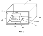
- FIG. 17 illustrates another charging device 420 having at least one interface 421 , according to an exemplary embodiment of the present invention.
- Charging device 420 may be configured to wirelessly charge at least one electronic device being positioned within an internal region 423 . More specifically, charging device 420 may include at least one transmit antenna (e.g., transmit antenna 114 depicted in FIG. 2 ) configured to wirelessly transmit power to a receive antenna (e.g., receive antenna 118 depicted in FIG. 2 ) and an associated receiver (e.g., receiver 108 depicted in FIG. 2 ) coupled to a battery (e.g., battery 136 depicted in FIG. 2 ) of an electronic device positioned within internal region 423 .
- transmit antenna e.g., transmit antenna 114 depicted in FIG. 2
- receive antenna e.g., receive antenna 118 depicted in FIG. 2
- an associated receiver e.g., receiver 108 depicted in FIG. 2
- battery e.g., battery
- multi-dimensional regions with multiple antennas may be performed by the techniques described herein.
- multi-dimensional wireless powering and charging may be employed, such as the means described in U.S. patent application Ser. No. 12/567,339, entitled “SYSTEMS AND METHOD RELATING TO MULTI-DIMENSIONAL WIRELESS CHARGING” filed on Sep. 25, 2009, the contents of which are hereby incorporated by reference in its entirety for all purposes.
- power may be supplied to the battery of the electronic device.
- charging device 420 includes interface 421 positioned on an exterior surface of charging device 420 and configured to convey graphics, alphanumeric text, or any combination thereof.
- Interface 421 may be configured to convey information relating to one or more electronic devices positioned within a charging region (i.e., internal region 423 ) of charging device 420 .
- interface 421 may be configured to convey an identifier of electronic device positioned within associated charging region.
- interface 421 may be configured to display a device label (e.g., a user name), a device type (e.g., cell phone, camera, etc.), or any combination thereof.
- interface 421 may be configured to display alphanumeric text (e.g., “Phone”) identifying the cellular telephone positioned within the charging region of charging device 420 .
- alphanumeric text e.g., “Phone”
- interface 421 may be configured to convey information related to a charging status of one or more electronic devices positioned within the charging region of charging device 420 .
- interface 421 may be configured to display one or more lights in display elements 425 , positioned proximate a device identifier (e.g., “Camera”), in a distinguishable pattern to indicate whether an associated electronic device within the charging region of charging device 420 is being charged.
- a device identifier e.g., “Camera”
- interface 421 may be configured to display one or more lights in another distinguishable pattern to indicate that an associated electronic device within a charging region of charging device 420 is fully charged.
- interface 421 may be configured to display one or more continuous lights associated with a device identifier to indicate that the electronic device is fully charged.
- charging device 420 may be configured to convey audio. More specifically, for example, interface 421 may be configured to audibly convey an identifier such as a device label (e.g., a user name), a device type (e.g., cell phone, camera, etc.), or any combination thereof. Additionally, interface 421 may be configured to audibly convey information indicative of whether an associated electronic device positioned within a charging region of charging device 420 is being charged or whether an associated electronic device positioned within the charging region of charging device 420 is fully charged.
- a device label e.g., a user name
- a device type e.g., cell phone, camera, etc.
- interface 421 may be configured to audibly identify the camera (e.g., audibly convey “camera”) and audibly convey a charging status of the camera (e.g., audibly convey “charged”).
- audibly identify the camera e.g., audibly convey “camera”
- audibly convey a charging status of the camera e.g., audibly convey “charged”.
- the exemplary embodiments described above depict one or more devices (i.e., chargeable electronic devices and/or non-chargeable devices) positioned directly on a surface of a charging device
- the charging devices described above may be configured to charge and convey information concerning any chargeable electronic device positioned within a near-field of a transmit antenna integrated within the charging device.
- any one of the charging devices described above may be configured to charge and convey information concerning a chargeable electronic device that is positioned within a portable device such as, for example, a purse, a backpack, or a briefcase.
- a portable device e.g., a bag having a chargeable electronic device therein may be placed in and/or on any of the charging devices, as described hererin, and the charging device may charge and convey information identifying the chargeable electronic device and a charging status of the chargeable electronic device.
- charging device 420 and more specifically interface 421 , may be configured to convey information concerning one or more chargeable electronic devices positioned within a portable device 427 , such as a bag, which is positioned within internal region 423 of charging device 420 .
- a portable device may include a repeater antenna, as described above, and, therefore, one or more chargeable electronic devices within the portable device may be charged via a charging device having a transmit antenna (e.g., charging device 420 ) and portable device having a repeater antenna (e.g., portable device 427 ).
- each charging device as described herein may be implemented as, for example only, a portable charging device such as a backpack, a briefcase, a purse, clothing, luggage, etc. Accordingly, portable device 427 , as described with reference to FIG.
- each charging device described herein may be implemented as, for example, a stationary charging device such as a table, a desk, or any other stationary furniture.
- FIG. 18 illustrates a wirelessly chargeable electronic device 922 .
- Device 922 may comprise any wirelessly chargeable electronic device such as, for example only, a cellular telephone, a portable media player, a camera, or any combination thereof.
- Device 922 may include an interface 924 and may be configured to convey a visible and/or an audible message to alert a device user that device 922 needs to be charged. More specifically, when an amount of available power stored in device 922 drops to or below a specific threshold level, device 922 may display and/or audibly convey an alert (e.g. a beep) to notify the user that device 922 requires charging.
- the threshold level may be determined based on an amount of power available in a battery of device 922 , an amount of battery time remaining based on user usage patterns and power consumption of device 922 , or any combination thereof.
- device 922 may be configured to audibly convey and/or display information concerning one or more wireless chargers, which may be configured to wirelessly charge device 922 . More specifically, in one exemplary embodiment, device 922 may be configured to display a map illustrating locations of one or more wireless chargers configured to wirelessly charge device 922 . In another exemplary embodiment, device 922 may be configured to provide a location, via text and/or an audible message, of one or more wireless chargers configured to wirelessly charge device 922 . Furthermore, in another exemplary embodiment, device 922 may be configured to audibly convey and/or display navigational directions to the one or more wireless chargers.
- device 922 may be configured to provide a user with a location of, and navigation directions to, one or more wireless chargers that are closest to device 922 .
- device 922 may be configured to display an alert (e.g., “Recharge”) and provide a link (“nearby tray”) to information (e.g., location, map, and/or navigational directions) concerning a nearby wireless charger.
- an alert e.g., “Recharge”
- a link e.g., location, map, and/or navigational directions
- device 922 may be configured to obtain information concerning wireless charger locations via any known and suitable detection means and/or through a populated database 926 .
- FIG. 19 is a flowchart illustrating a method 900 of operating a wireless charging device, in accordance with one or more exemplary embodiments.
- Method 900 may include wirelessly transmitting power to one or more electronic devices positioned within a charging region of a charging device (depicted by numeral 902 ).
- Method 900 may further include conveying information related to at least one electronic device of the one or more electronic devices (depicted by numeral 904 ).
- FIG. 20 is a flowchart illustrating another method 910 of operating a wireless charging device, according to one or more exemplary embodiments.
- Method 910 may include transmitting wireless power to one or more electronic devices (depicted by numeral 912 ). Furthermore, method 910 may include conveying information related to a charging status of at least one electronic device of the one or more electronic devices (depicted by numeral 914 ).
- Various exemplary embodiments of the present invention may enable a user of a charging device, as described above, to be informed of a charging status of one or more electronic devices, which are positioned within a charging region of the charging device, and which may or may not be visible to the user.
- DSP Digital Signal Processor
- ASIC Application Specific Integrated Circuit
- FPGA Field Programmable Gate Array
- a general purpose processor may be a microprocessor, but in the alternative, the processor may be any conventional processor, controller, microcontroller, or state machine.
- a processor may also be implemented as a combination of computing devices, e.g., a combination of a DSP and a microprocessor, a plurality of microprocessors, one or more microprocessors in conjunction with a DSP core, or any other such configuration.
- a software module may reside in Random Access Memory (RAM), flash memory, Read Only Memory (ROM), Electrically Programmable ROM (EPROM), Electrically Erasable Programmable ROM (EEPROM), registers, hard disk, a removable disk, a CD-ROM, or any other form of storage medium known in the art.
- An exemplary storage medium is coupled to the processor such that the processor can read information from, and write information to, the storage medium.
- the storage medium may be integral to the processor.
- the processor and the storage medium may reside in an ASIC.
- the ASIC may reside in a user terminal.
- the processor and the storage medium may reside as discrete components in a user terminal.
- the functions described may be implemented in hardware, software, firmware, or any combination thereof. If implemented in software, the functions may be stored on or transmitted over as one or more instructions or code on a computer-readable medium.
- Computer-readable media includes both computer storage media and communication media including any medium that facilitates transfer of a computer program from one place to another.
- a storage media may be any available media that can be accessed by a computer.
- such computer-readable media can comprise RAM, ROM, EEPROM, CD-ROM or other optical disk storage, magnetic disk storage or other magnetic storage devices, or any other medium that can be used to carry or store desired program code in the form of instructions or data structures and that can be accessed by a computer.
- any connection is properly termed a computer-readable medium.
- the software is transmitted from a website, server, or other remote source using a coaxial cable, fiber optic cable, twisted pair, digital subscriber line (DSL), or wireless technologies such as infrared, radio, and microwave
- the coaxial cable, fiber optic cable, twisted pair, DSL, or wireless technologies such as infrared, radio, and microwave are included in the definition of medium.
- Disk and disc includes compact disc (CD), laser disc, optical disc, digital versatile disc (DVD), floppy disk and blu-ray disc where disks usually reproduce data magnetically, while discs reproduce data optically with lasers. Combinations of the above should also be included within the scope of computer-readable media.
Abstract
Description
| TABLE 1 | |||
| Efficiency (TX | |||
| Distance from | S21 efficiency | DC power in to | |
| Position | plane (cm) | (%) | RX DC power out) |
| |
0 | 46.8 | 28 |
| |
0 | 55.0 | 36 |
| |
0 | 57.5 | 35 |
| p4 | 2.5 | 49.0 | 30 |
| p5 | 17.5 | 24.5 | 15 |
| p6 | 17.5 | 0.3 | 0.2 |
| |
0 | 5.9 | 3.4 |
Claims (37)
Priority Applications (3)
| Application Number | Priority Date | Filing Date | Title |
|---|---|---|---|
| US12/572,371 US8854224B2 (en) | 2009-02-10 | 2009-10-02 | Conveying device information relating to wireless charging |
| TW099104284A TW201130204A (en) | 2009-02-10 | 2010-02-10 | Conveying device information relating to wireless charging |
| PCT/US2010/023796 WO2010093729A1 (en) | 2009-02-10 | 2010-02-10 | Conveying device information relating to wireless charging |
Applications Claiming Priority (3)
| Application Number | Priority Date | Filing Date | Title |
|---|---|---|---|
| US15129009P | 2009-02-10 | 2009-02-10 | |
| US15236309P | 2009-02-13 | 2009-02-13 | |
| US12/572,371 US8854224B2 (en) | 2009-02-10 | 2009-10-02 | Conveying device information relating to wireless charging |
Publications (2)
| Publication Number | Publication Date |
|---|---|
| US20100201533A1 US20100201533A1 (en) | 2010-08-12 |
| US8854224B2 true US8854224B2 (en) | 2014-10-07 |
Family
ID=42539978
Family Applications (1)
| Application Number | Title | Priority Date | Filing Date |
|---|---|---|---|
| US12/572,371 Active 2032-03-16 US8854224B2 (en) | 2009-02-10 | 2009-10-02 | Conveying device information relating to wireless charging |
Country Status (3)
| Country | Link |
|---|---|
| US (1) | US8854224B2 (en) |
| TW (1) | TW201130204A (en) |
| WO (1) | WO2010093729A1 (en) |
Cited By (8)
| Publication number | Priority date | Publication date | Assignee | Title |
|---|---|---|---|---|
| US20130043734A1 (en) * | 2011-08-16 | 2013-02-21 | Qualcomm Incorporated | Wireless power receiver with multiple receiver coils |
| US20140266025A1 (en) * | 2013-03-15 | 2014-09-18 | Daniel B. Jakubowski | Wireless interrogation and wireless charging of electronic devices |
| US20150207357A1 (en) * | 2014-01-23 | 2015-07-23 | Electronics And Telecommunications Research Institute | Wireless power transmission device, wireless power reception device and wireless power transmission system |
| US20150249360A1 (en) * | 2012-09-05 | 2015-09-03 | Renesas Electronics Corporation | Non-contact charging device, and non-contact power supply system using same |
| US9312924B2 (en) | 2009-02-10 | 2016-04-12 | Qualcomm Incorporated | Systems and methods relating to multi-dimensional wireless charging |
| US9391476B2 (en) | 2010-09-09 | 2016-07-12 | Semiconductor Energy Laboratory Co., Ltd. | Power feeding device, wireless power feeding system using the same and wireless power feeding method |
| US9607459B2 (en) * | 2015-05-25 | 2017-03-28 | Hon Hai Precision Industry Co., Ltd. | Wirelessly charging electronic lock device |
| US9954399B2 (en) | 2008-05-13 | 2018-04-24 | Qualcomm Incorporated | Reverse link signaling via receive antenna impedance modulation |
Families Citing this family (39)
| Publication number | Priority date | Publication date | Assignee | Title |
|---|---|---|---|---|
| US8878393B2 (en) | 2008-05-13 | 2014-11-04 | Qualcomm Incorporated | Wireless power transfer for vehicles |
| US20100201312A1 (en) * | 2009-02-10 | 2010-08-12 | Qualcomm Incorporated | Wireless power transfer for portable enclosures |
| US20100201201A1 (en) * | 2009-02-10 | 2010-08-12 | Qualcomm Incorporated | Wireless power transfer in public places |
| US20100201311A1 (en) * | 2009-02-10 | 2010-08-12 | Qualcomm Incorporated | Wireless charging with separate process |
| US9124308B2 (en) | 2009-05-12 | 2015-09-01 | Kimball International, Inc. | Furniture with wireless power |
| WO2010132578A1 (en) | 2009-05-12 | 2010-11-18 | Kimball International, Inc. | Furniture with wireless power |
| JP2011017619A (en) * | 2009-07-09 | 2011-01-27 | Mitsumi Electric Co Ltd | Battery pack, semiconductor device, portable device, notification method, and notification program |
| US10343535B2 (en) * | 2010-04-08 | 2019-07-09 | Witricity Corporation | Wireless power antenna alignment adjustment system for vehicles |
| JP2012019666A (en) * | 2010-07-09 | 2012-01-26 | Sony Corp | Wireless charging device and wireless charging system |
| US9438063B2 (en) | 2010-07-09 | 2016-09-06 | Industrial Technology Research Institute | Charge apparatus |
| US10211664B2 (en) | 2010-07-09 | 2019-02-19 | Industrial Technology Research Institute | Apparatus for transmission of wireless energy |
| US20120104997A1 (en) * | 2010-11-01 | 2012-05-03 | Qualcomm Incorporated | Wireless charging device |
| US20120246569A1 (en) * | 2011-03-22 | 2012-09-27 | Eric Liu | Generating a personal topology during inductive charging and data transfer |
| US9496925B2 (en) | 2011-09-30 | 2016-11-15 | Nokia Technologies Oy | Method, apparatus, and computer program product for remote wireless powering and control of an electronic device |
| US9806537B2 (en) | 2011-12-15 | 2017-10-31 | Samsung Electronics Co., Ltd | Apparatus and method for determining whether a power receiver is removed from the apparatus |
| WO2013114507A1 (en) * | 2012-02-03 | 2013-08-08 | 日本電気株式会社 | Electromagnetic wave transmission sheet, and electromagnetic wave transmission device |
| EP2810356A1 (en) * | 2012-02-05 | 2014-12-10 | Humavox Ltd. | Remote charging system |
| US8933589B2 (en) | 2012-02-07 | 2015-01-13 | The Gillette Company | Wireless power transfer using separately tunable resonators |
| KR20130098521A (en) * | 2012-02-28 | 2013-09-05 | 삼성전자주식회사 | Wireless power providing device and method for controlling thereof |
| TWI456859B (en) * | 2012-03-02 | 2014-10-11 | Hsiung Kuang Tsai | Wireless power transmission system |
| CN104584372B (en) * | 2012-08-31 | 2017-07-04 | 西门子公司 | For battery charging system and method to battery wireless charging |
| JP6111583B2 (en) * | 2012-10-01 | 2017-04-12 | 株式会社Ihi | Contactless power supply system |
| JP6160288B2 (en) | 2013-03-04 | 2017-07-12 | 船井電機株式会社 | Power supply device |
| US9287722B2 (en) | 2013-03-15 | 2016-03-15 | Donald S. Williams | Personal e-port apparatus |
| US9203252B2 (en) * | 2013-11-12 | 2015-12-01 | Google Inc. | Redirecting notifications to a wearable computing device |
| US9171434B2 (en) | 2014-03-12 | 2015-10-27 | Google Inc. | Selectively redirecting notifications to a wearable computing device |
| US9313610B2 (en) * | 2014-03-28 | 2016-04-12 | Intel Corporation | On demand customization of mobile computing devices |
| WO2015183336A1 (en) | 2014-05-30 | 2015-12-03 | Apple Inc. | Battery usage tracking user interface |
| WO2016022496A2 (en) | 2014-08-06 | 2016-02-11 | Apple Inc. | Reduced-size user interfaces for battery management |
| KR102231851B1 (en) * | 2014-09-25 | 2021-03-26 | 삼성전자주식회사 | A method for recharging one or more eelectronic devices and a recharging apparatus therefor |
| US20160190817A1 (en) * | 2014-09-30 | 2016-06-30 | Jeremy Hartelt | Wireless power transfer bag for mobile devices |
| US20160233707A1 (en) * | 2015-02-06 | 2016-08-11 | Michael Kidakarn | Power Adapter with Charging Data Display |
| US10164484B2 (en) | 2015-06-08 | 2018-12-25 | Ossia Inc. | Techniques for leveraging existing components of a device for wireless power transfer functionality |
| GB2543799B (en) * | 2015-10-28 | 2018-11-28 | Displaylink Uk Ltd | Remote wake-up of mobile devices |
| WO2017209630A1 (en) | 2016-06-01 | 2017-12-07 | Powerbyproxi Limited | A powered joint with wireless transfer |
| US10951043B2 (en) | 2017-06-04 | 2021-03-16 | Apple Inc. | Multi-device charging user interface |
| US10938253B2 (en) | 2017-09-08 | 2021-03-02 | Apple Inc. | Wireless power system with battery charge indicators |
| US11646591B2 (en) | 2019-05-09 | 2023-05-09 | Apple Inc. | Indication for protective charging mode |
| EP3806284A1 (en) * | 2019-10-10 | 2021-04-14 | Vestel Elektronik Sanayi ve Ticaret A.S. | Apparatus and method for wirelessly charging mobile devices, and mobile device |
Citations (305)
| Publication number | Priority date | Publication date | Assignee | Title |
|---|---|---|---|---|
| US3633109A (en) | 1967-10-21 | 1972-01-04 | Saba Schwarzwalder Apparati Ba | Negative resistance antenna amplifier arrangement |
| JPS5931054U (en) | 1982-08-23 | 1984-02-27 | 日本電子機器株式会社 | oxygen sensor |
| US4684869A (en) | 1982-03-24 | 1987-08-04 | Terumo Kabushiki Kaisha | Electronic clinical thermometer |
| US4802080A (en) | 1988-03-18 | 1989-01-31 | American Telephone And Telegraph Company, At&T Information Systems | Power transfer circuit including a sympathetic resonator |
| DE4004196C1 (en) | 1990-02-12 | 1991-04-11 | Texas Instruments Deutschland Gmbh, 8050 Freising, De | Transponder transferring stored measurement data to interrogator - operates without battery using capacitor charged by rectified HF pulses |
| EP0444416A1 (en) | 1990-01-26 | 1991-09-04 | Pioneer Electronic Corporation | Motor vehicle-mounted radio wave receiving GPS apparatus |
| US5201066A (en) | 1990-07-25 | 1993-04-06 | Hyundai Electronics Industries Co., Ltd. | Radio-telephone system employing a manner of changing a channel and a privacy digital code and interstoring them between a stationary apparatus and a portable apparatus by wireless and a method of changing the privacy digital code |
| US5287112A (en) | 1993-04-14 | 1994-02-15 | Texas Instruments Incorporated | High speed read/write AVI system |
| JPH06112720A (en) | 1992-09-30 | 1994-04-22 | Casio Comput Co Ltd | Radio receiver |
| US5520892A (en) | 1994-04-11 | 1996-05-28 | Bowen; John G. | Sterilization unit for dental handpieces and other instruments |
| US5539394A (en) | 1994-03-16 | 1996-07-23 | International Business Machines Corporation | Time division multiplexed batch mode item identification system |
| US5619530A (en) | 1994-04-04 | 1997-04-08 | Motorola, Inc. | Method and apparatus for detecting and handling collisions in a radio communication system |
| JPH09103037A (en) | 1995-10-05 | 1997-04-15 | Nippon Ido Tsushin Kk | Power supply unit, unit to be supplied with power and power supply system |
| JPH09147070A (en) | 1995-11-20 | 1997-06-06 | Sony Corp | Noncontact type information card |
| DE29710675U1 (en) | 1997-06-16 | 1997-08-14 | Tegethoff Marius | Display system for vehicles |
| JPH10145987A (en) | 1996-09-13 | 1998-05-29 | Hitachi Ltd | Power transmission system, ic card and information communicating system using ic card |
| US5790080A (en) | 1995-02-17 | 1998-08-04 | Lockheed Sanders, Inc. | Meander line loaded antenna |
| JPH10210751A (en) | 1997-01-22 | 1998-08-07 | Hitachi Ltd | Rectifying circuit and semiconductor integrated circuit and ic card |
| WO1998029969A3 (en) | 1996-12-30 | 1998-09-11 | At & T Corp | Communication terminal having proximity detector method and apparatus for safe wireless communication |
| JPH10240880A (en) | 1997-02-26 | 1998-09-11 | Rohm Co Ltd | Ic card system and carriage system using the same |
| JPH10295043A (en) | 1997-04-16 | 1998-11-04 | Fujiden Enji Kk | Power supply for portable electronic apparatus |
| JPH10293826A (en) | 1986-09-11 | 1998-11-04 | Asahi Denshi Kk | Power and information non-contact transmitting device provided with link head |
| WO1998054912A1 (en) | 1997-05-30 | 1998-12-03 | Scs Corporation | Cloaking circuit for use in a radio frequency identification and method of cloaking rfid tags to increase interrogation reliability |
| JPH1125238A (en) | 1997-07-04 | 1999-01-29 | Kokusai Electric Co Ltd | Ic card |
| WO1999005658A1 (en) | 1997-07-25 | 1999-02-04 | Checkpoint Systems, Inc. | Electrically, physically or virtually reactivating rfid tags |
| JPH1169640A (en) | 1997-08-26 | 1999-03-09 | Matsushita Electric Works Ltd | Non-contact charging device |
| JPH1198706A (en) | 1997-09-18 | 1999-04-09 | Tokin Corp | Non-contact charger |
| JPH11122832A (en) | 1997-10-07 | 1999-04-30 | Casio Comput Co Ltd | Charger |
| JPH11134566A (en) | 1997-10-31 | 1999-05-21 | Takenaka Engineering Kogyo Kk | Ogject detector with wireless power supply device |
| JPH11155245A (en) | 1997-11-21 | 1999-06-08 | Shinko Electric Co Ltd | Primary power supply side power device in non-contact power supply |
| JPH11188113A (en) | 1997-12-26 | 1999-07-13 | Nec Corp | Power transmission system, power transmission method and electric stimulation device provided with the power transmission system |
| US5956626A (en) | 1996-06-03 | 1999-09-21 | Motorola, Inc. | Wireless communication device having an electromagnetic wave proximity sensor |
| EP0977304A1 (en) | 1998-07-28 | 2000-02-02 | Koninklijke Philips Electronics N.V. | Communication apparatus, mobile radio equipment, base station and procedure to control the output power |
| JP2000501263A (en) | 1995-11-27 | 2000-02-02 | テレフオンアクチーボラゲツト エル エム エリクソン(パブル) | Impedance means |
| JP2000050534A (en) | 1998-08-03 | 2000-02-18 | Shiro Sugimura | Power supply apparatus for ic card |
| JP2000057450A (en) | 1998-06-04 | 2000-02-25 | Mitsubishi Materials Corp | Burglar prevention tag and using method thereof |
| JP2000067195A (en) | 1998-08-26 | 2000-03-03 | Sony Corp | Information card |
| JP2000113127A (en) | 1998-09-30 | 2000-04-21 | Toshiba Corp | Wireless tag system |
| WO2000027137A1 (en) | 1998-11-04 | 2000-05-11 | Checkpoint Systems, Inc. | Rfid tag having parallel resonant circuit for magnetically decoupling tag from its environment |
| JP2000172795A (en) | 1998-12-07 | 2000-06-23 | Kokusai Electric Co Ltd | Reader/writer |
| EP1022677A1 (en) | 1996-12-27 | 2000-07-26 | Rohm Co., Ltd. | Responder, integrated circuit chip, noncontact ic card, and self power needless type device in noncontact ic card communication system, and automatic adjustment method for self power needless type device |
| EP1050839A1 (en) | 1999-05-04 | 2000-11-08 | CS Systemes d'Informations | Wireless chip card reader having a regulated emitted power |
| US6151500A (en) * | 1997-06-20 | 2000-11-21 | Bellsouth Corporation | Method and apparatus for directing a wireless communication to a wireline unit |
| US6195562B1 (en) | 1996-11-13 | 2001-02-27 | Nokia Mobile Phones Ltd. | System for limiting the transmitted power of a mobile communication means |
| US20010000960A1 (en) | 1998-05-18 | 2001-05-10 | Dettloff Wayne D. | Systems and methods for wirelessly projecting power using multiple in-phase current loops |
| US6263247B1 (en) | 1998-06-09 | 2001-07-17 | North Carolina State University | System and method for powering, controlling, and communicating with multiple inductively-powered devices |
| EP0689149B1 (en) | 1994-06-21 | 2001-08-22 | Sony Chemicals Corporation | Non-contacting information cards |
| JP2001238372A (en) | 2000-02-24 | 2001-08-31 | Nippon Telegr & Teleph Corp <Ntt> | Power transmission system, electromagnetic field generator, and electromagnetic field receiver |
| JP2001291080A (en) | 2000-04-07 | 2001-10-19 | Nippon Signal Co Ltd:The | Non-contact type ic card |
| JP2001309579A (en) | 2000-04-25 | 2001-11-02 | Matsushita Electric Works Ltd | Non-contact power feeding apparatus |
| US20010046205A1 (en) | 1994-09-30 | 2001-11-29 | Easton Kenneth D. | Multipath search processor for a spread spectrum multiple access communication system |
| JP2002034169A (en) | 2000-07-14 | 2002-01-31 | Sanyo Electric Co Ltd | Noncontact charger and portable telephone |
| DE10104019C1 (en) | 2001-01-31 | 2002-01-31 | Bosch Gmbh Robert | Motor cycle protective suit with airbag(s) has connection arrangement to trigger device on motor cycle formed by coil(s) for acquiring energy and data transmission radio terminal(s) |
| US6344828B1 (en) | 1998-12-17 | 2002-02-05 | Daimlerchrysler Ag | Antenna system for a satellite-supported vehicle navigation device |
| JP2002050534A (en) | 2000-08-04 | 2002-02-15 | Taiyo Yuden Co Ltd | Electronic component |
| WO2002027682A1 (en) | 2000-09-25 | 2002-04-04 | Motorola, Inc. | Method and apparatus for selectively activating radio frequency identification tags that are in close proximity |
| US20020041624A1 (en) | 2000-10-11 | 2002-04-11 | Kim Kwang Soon | Finger using time division method and rake receiver having the same |
| WO2002062077A1 (en) | 2001-01-23 | 2002-08-08 | Single Chip Systems Corporation | A selective cloaking circuit for use in a radiofrequency identification and method of cloaking rfid tags |
| US20020154705A1 (en) | 2000-03-22 | 2002-10-24 | Walton Jay R. | High efficiency high performance communications system employing multi-carrier modulation |
| US20020158512A1 (en) | 2001-04-26 | 2002-10-31 | Satoshi Mizutani | Mounting structure including communication system for transmitting multiplex control signal to vehicle electrical devices |
| US6489745B1 (en) | 2001-09-13 | 2002-12-03 | The Boeing Company | Contactless power supply |
| JP2003047178A (en) | 1992-10-13 | 2003-02-14 | Sony-Kihara Research Center Inc | Wireless power receiving device |
| EP1298578A1 (en) | 2001-01-26 | 2003-04-02 | Sony Corporation | Noncontact ic card |
| WO2003044970A2 (en) | 2001-11-20 | 2003-05-30 | Qualcomm Incorporated | Reverse link power controlled repeater |
| CN1426170A (en) | 2001-12-12 | 2003-06-25 | 天瀚科技股份有限公司 | Radio electromagnetic pressure induction system |
| US6600931B2 (en) | 2001-03-30 | 2003-07-29 | Nokia Corporation | Antenna switch assembly, and associated method, for a radio communication station |
| JP2003224937A (en) | 2002-01-25 | 2003-08-08 | Sony Corp | Method and apparatus for power supply, method and apparatus for receiving power supply, power supply system, recording medium, and program |
| US6608550B2 (en) | 1997-06-20 | 2003-08-19 | Hitachi, Ltd. | Reader and/or writer apparatus, power feeding system, and communication system |
| WO2003079524A2 (en) | 2002-03-13 | 2003-09-25 | Celis Semiconductor Corporation | Rectifier utilizing a grounded antenna |
| TW200306048A (en) | 2002-04-08 | 2003-11-01 | Alps Electric Co Ltd | Charging chamber and charging reservoir |
| US6664770B1 (en) | 1999-12-05 | 2003-12-16 | Iq- Mobil Gmbh | Wireless power transmission system with increased output voltage |
| US20040002835A1 (en) | 2002-06-26 | 2004-01-01 | Nelson Matthew A. | Wireless, battery-less, asset sensor and communication system: apparatus and method |
| US6683438B2 (en) | 2001-01-05 | 2004-01-27 | Samsung Electronics Co., Ltd. | Contactless battery charger |
| US20040041669A1 (en) | 2002-09-03 | 2004-03-04 | Kazuo Kawai | Tuning circuit |
| WO2004025805A1 (en) | 2002-09-12 | 2004-03-25 | Mitsubishi Denki Kabushiki Kaisha | Receiving device, display device, power supply system, display system, and receiving method |
| WO2004032349A1 (en) | 2002-10-02 | 2004-04-15 | Batelle Memorial Institute | Radio frequency identification devices, backscatter communication device wake-up methods, communication device wake-up methods and a radio frequency identification device wake-up method |
| JP2004135455A (en) | 2002-10-11 | 2004-04-30 | Denso Corp | Ic card, electronic apparatus, and power feeder thereof |
| JP2004159456A (en) | 2002-11-07 | 2004-06-03 | Iden Videotronics:Kk | Energy supplier |
| US20040116952A1 (en) | 1999-03-05 | 2004-06-17 | Olympus Optical Co., Ltd. | Surgical apparatus permitting recharge of battery-driven surgical instrument in noncontact state |
| WO2004055654A2 (en) | 2002-12-16 | 2004-07-01 | Splashpower Limited | Adapting portable electrical devices to receive power wirelessly |
| US6760578B2 (en) | 1993-07-15 | 2004-07-06 | Micron Technology, Inc. | Wake up device for a communications system |
| US20040130425A1 (en) | 2002-08-12 | 2004-07-08 | Tal Dayan | Enhanced RF wireless adaptive power provisioning system for small devices |
| US20040130916A1 (en) | 1999-06-21 | 2004-07-08 | Baarman David W. | Adaptive inductive power supply |
| US20040145342A1 (en) | 2003-01-28 | 2004-07-29 | Lyon Geoff M. | Adaptive charger system and method |
| US20040154652A1 (en) | 2003-02-10 | 2004-08-12 | Armen Karapetyan | Cleaning apparatus for medical and/or dental tool |
| KR20040072581A (en) | 2004-07-29 | 2004-08-18 | (주)제이씨 프로텍 | An amplification relay device of electromagnetic wave and a radio electric power conversion apparatus using the above device |
| WO2004073166A2 (en) | 2003-02-04 | 2004-08-26 | Access Business Group International Llc | Adaptive inductive power supply with communication |
| US20040166869A1 (en) | 2003-02-19 | 2004-08-26 | Rajiv Laroia | Controlled superposition coding in multi-user communication systems |
| EP1454769A1 (en) | 2003-03-03 | 2004-09-08 | Sokymat Identifikations Komponenten GmbH | Apparatus for inductively transmitting signals between a transponder circuit and an interrogating circuit |
| US20040180637A1 (en) | 2003-03-11 | 2004-09-16 | Nobuyuki Nagai | Wireless communication IC and wireless communication information storage medium using the same |
| JP2004274972A (en) | 2003-03-12 | 2004-09-30 | Toshiba Corp | Cable-less power supply apparatus |
| JP2004297779A (en) | 2003-03-11 | 2004-10-21 | Hitachi Maxell Ltd | Radio communications ic and radio communication information storage medium using the same |
| US6809498B2 (en) | 2001-05-18 | 2004-10-26 | Seiko Instruments Inc. | Power supply apparatus and electronic equipment |
| JP2004306558A (en) | 2003-04-10 | 2004-11-04 | Seiko Epson Corp | Non-contact communication between device and its consumable article container |
| WO2004096023A1 (en) | 2003-04-25 | 2004-11-11 | Olympus Corporation | Radio-type in-subject information acquisition system and outside-subject device |
| US20040227057A1 (en) | 2003-04-17 | 2004-11-18 | Ailocom Oy | Wireless power transmission |
| JP2004355212A (en) | 2003-05-28 | 2004-12-16 | Matsushita Electric Ind Co Ltd | Non-contact type ic card reader/writer and adjusting method therefor |
| EP1502543A1 (en) | 2003-07-29 | 2005-02-02 | Biosense Webster, Inc. | Energy transfer amplification for intrabody devices |
| US6853629B2 (en) | 1997-02-06 | 2005-02-08 | Cingular Wireless Ii, Llc | Method for frequency division duplex communications |
| CN2681368Y (en) | 2004-03-16 | 2005-02-23 | 周彬 | A pad pasting for wireless rechargeable battery |
| US20050068019A1 (en) | 2003-09-30 | 2005-03-31 | Sharp Kabushiki Kaisha | Power supply system |
| JP2005110412A (en) | 2003-09-30 | 2005-04-21 | Sharp Corp | Power supply system |
| US20050083881A1 (en) | 2002-01-23 | 2005-04-21 | Hideki Ohwada | Base station and mobile communication system utilizing the same |
| JP2005135455A (en) | 2003-10-28 | 2005-05-26 | Tdk Corp | Manufacturing method of magnetic recording medium |
| US20050116683A1 (en) | 2002-05-13 | 2005-06-02 | Splashpower Limited | Contact-less power transfer |
| US6906495B2 (en) | 2002-05-13 | 2005-06-14 | Splashpower Limited | Contact-less power transfer |
| JP2005159607A (en) | 2003-11-25 | 2005-06-16 | Matsushita Electric Ind Co Ltd | Portable communication apparatus |
| US20050151511A1 (en) | 2004-01-14 | 2005-07-14 | Intel Corporation | Transferring power between devices in a personal area network |
| JP2005204493A (en) | 2003-12-19 | 2005-07-28 | Semiconductor Energy Lab Co Ltd | Semiconductor device and driving method therefor |
| JP2005208754A (en) | 2004-01-20 | 2005-08-04 | Matsushita Electric Ind Co Ltd | Non-contact ic card communication equipment |
| JP2005224045A (en) | 2004-02-06 | 2005-08-18 | Mitsubishi Heavy Ind Ltd | Non-contact power feeding device and wire-less system provided with it |
| US20050205679A1 (en) | 2004-03-17 | 2005-09-22 | Infineon Technologies Ag | Rectifier circuit |
| JP2005261187A (en) | 2004-02-12 | 2005-09-22 | Kansai Tlo Kk | Wireless power supply system |
| US20050219132A1 (en) | 2002-11-12 | 2005-10-06 | Inside Contactless | Tunable antenna circuit, particularly for contactless integrated circuit reader |
| US20050220057A1 (en) | 1999-06-01 | 2005-10-06 | Peter Monsen | Multiple access system and method for multibeam digital radio systems |
| EP1585268A2 (en) | 1995-05-26 | 2005-10-12 | SimonsVoss Technologies AG | System for data transfer including a circuit for saving energy |
| US20050225437A1 (en) | 2004-04-13 | 2005-10-13 | Fujitsu Limited | Information processing apparatus for receiving predetermined information, and program product and method therefor |
| US20050239018A1 (en) | 2004-04-27 | 2005-10-27 | Scott Green | Intraoral bite spacer and illumination apparatus |
| WO2005104022A1 (en) | 2004-04-08 | 2005-11-03 | 3M Innovative Properties Company | Variable frequency radio frequency identification (rfid) tags |
| US6967462B1 (en) | 2003-06-05 | 2005-11-22 | Nasa Glenn Research Center | Charging of devices by microwave power beaming |
| US6970142B1 (en) | 2001-08-16 | 2005-11-29 | Raytheon Company | Antenna configurations for reduced radar complexity |
| EP0831411B1 (en) | 1996-09-19 | 2005-12-07 | Kabushiki Kaisha Toshiba | Reader/writer for performing efficient transmission/reception with no-battery information storage medium |
| GB2380359B (en) | 2001-09-28 | 2005-12-07 | Agere Systems Inc | A proximity regulation system for use with a portable cell phone and a method of operation thereof |
| CN1722521A (en) | 2004-05-18 | 2006-01-18 | 爱莎·艾伯莱鉴定科技集团有限公司 | Antenna array for an RFID reader compatible with transponders operating at different carrier frequencies |
| JP2006060909A (en) | 2004-08-19 | 2006-03-02 | Seiko Epson Corp | Noncontact power transmitter |
| WO2006031133A1 (en) | 2004-09-16 | 2006-03-23 | Auckland Uniservices Limited | Inductively powered mobile sensor system |
| US20060084392A1 (en) | 2004-10-15 | 2006-04-20 | Broadcom Corporation | Transceiver system and method of using same |
| GB2395627B (en) | 2002-11-21 | 2006-05-10 | Hewlett Packard Co | Detector |
| US20060113955A1 (en) | 2004-11-29 | 2006-06-01 | Patrick Nunally | Remote power charging of electronic devices |
| JP2006141170A (en) | 2004-11-15 | 2006-06-01 | Sharp Corp | Power supply system and transmission device and receiving device for use in the system |
| US20060114102A1 (en) | 2004-11-26 | 2006-06-01 | Industrial Technology Research Institute | High performance RFID system and operating method thereof |
| JP2006149168A (en) | 2004-11-24 | 2006-06-08 | Fuji Electric Holdings Co Ltd | Non-contact power feeder apparatus |
| US20060131193A1 (en) | 2004-12-17 | 2006-06-22 | Depuy Products, Inc. | System for recharging medical instruments |
| US7069086B2 (en) | 2002-08-08 | 2006-06-27 | Cardiac Pacemakers, Inc. | Method and system for improved spectral efficiency of far field telemetry in a medical device |
| WO2006068416A1 (en) | 2004-12-21 | 2006-06-29 | Electronics And Telecommunications Research Institute | Ultra isolation antenna |
| JP2006174676A (en) | 2004-12-20 | 2006-06-29 | Nissan Motor Co Ltd | Microwave transmitting system for vehicle and microwave receiving apparatus for vehicle |
| TWM294779U (en) | 2006-01-06 | 2006-07-21 | Wen-Sung Li | Portable charging device of mobile phone |
| CN1808473A (en) | 2005-03-28 | 2006-07-26 | 上海中策工贸有限公司 | Wireless label electronic paper traffic sign |
| US20060184705A1 (en) | 2005-02-17 | 2006-08-17 | Yukio Nakajima | Communication system, digital camera and docking apparatus |
| CN1829037A (en) | 2005-03-03 | 2006-09-06 | 陈居阳 | Battery device with wireless charging system and its method |
| US20060197652A1 (en) | 2005-03-04 | 2006-09-07 | International Business Machines Corporation | Method and system for proximity tracking-based adaptive power control of radio frequency identification (RFID) interrogators |
| US20060202665A1 (en) | 2005-03-10 | 2006-09-14 | Microsoft Corporation | Inductive powering surface for powering portable devices |
| JP2006254678A (en) | 2005-03-07 | 2006-09-21 | Wise Media Technology Inc | Power charge box for rfid transponder |
| US20060220863A1 (en) | 2005-03-16 | 2006-10-05 | Semiconductor Energy Laboratory Co., Ltd. | Information processing device |
| EP1713145A1 (en) | 2004-02-02 | 2006-10-18 | Fujitsu Frontech Limited | Small loop antenna for induction reader/writer |
| JP2006296123A (en) | 2005-04-13 | 2006-10-26 | Yaskawa Electric Corp | Noncontact power supply system and power transmission method |
| JP2006295905A (en) | 2005-03-16 | 2006-10-26 | Semiconductor Energy Lab Co Ltd | Information processing apparatus |
| US20060244568A1 (en) | 2005-04-29 | 2006-11-02 | William Tong | Assembly for monitoring an environment |
| JP2006314181A (en) | 2005-05-09 | 2006-11-16 | Sony Corp | Non-contact charger, non-contact charging system, and non-contact charging method |
| US7142811B2 (en) | 2001-03-16 | 2006-11-28 | Aura Communications Technology, Inc. | Wireless communication over a transducer device |
| US7146139B2 (en) | 2001-09-28 | 2006-12-05 | Siemens Communications, Inc. | System and method for reducing SAR values |
| GB2416633B (en) | 2004-07-22 | 2006-12-06 | Lear Corp | Cellular telephone battery recharging apparatus |
| CN1881733A (en) | 2005-06-17 | 2006-12-20 | 乐金电子(沈阳)有限公司 | Wireless remote controller charging system |
| US20070004466A1 (en) * | 2003-03-28 | 2007-01-04 | Haartsen Jacobus C | Method and apparatus for calculating whether power level is sufficient for data transfer |
| US20070001816A1 (en) | 2005-06-30 | 2007-01-04 | Farpointe Data, Inc., A California Corporation | Power consumption management for an RFID reader |
| WO2007000055A1 (en) | 2005-06-28 | 2007-01-04 | Cynetic Designs Ltd. | Contactless battery charging apparel |
| JP2007006029A (en) | 2005-06-22 | 2007-01-11 | Sony Corp | Electronic equipment with built-in rfid |
| US7164255B2 (en) | 2002-06-10 | 2007-01-16 | City University Of Hong Kong | Inductive battery charger system with primary transformer windings formed in a multi-layer structure |
| US20070021140A1 (en) | 2005-07-22 | 2007-01-25 | Keyes Marion A Iv | Wireless power transmission systems and methods |
| US20070017804A1 (en) | 2005-07-22 | 2007-01-25 | Sandvik Intellectual Property Ab | Device for improving plasma activity PVD-reactors |
| CN1906863A (en) | 2003-11-26 | 2007-01-31 | 斯达克实验室公司 | Resonance frequency shift canceling in wireless hearing aids |
| US20070026799A1 (en) | 2005-07-28 | 2007-02-01 | D-Link Systems, Inc. | Wireless media device cradle |
| US20070029965A1 (en) | 2005-07-25 | 2007-02-08 | City University Of Hong Kong | Rechargeable battery circuit and structure for compatibility with a planar inductive charging platform |
| KR20070017804A (en) | 2005-08-08 | 2007-02-13 | (주)제이씨 프로텍 | A Small and Light Wireless Power Transmitting and Receiving Device |
| JP2007043773A (en) | 2005-08-01 | 2007-02-15 | Nissan Motor Co Ltd | Device and method for monitoring/controlling leakes of microwaves |
| US7193578B1 (en) | 2005-10-07 | 2007-03-20 | Lockhead Martin Corporation | Horn antenna array and methods for fabrication thereof |
| KR20070032271A (en) | 2003-11-25 | 2007-03-21 | 스타키 러보러토리즈 인코포레이티드 | Enhanced magnetic field communication system |
| US20070072474A1 (en) | 2005-04-27 | 2007-03-29 | Nigel Beasley | Flexible power adapter systems and methods |
| CN1941541A (en) | 2005-09-29 | 2007-04-04 | 英华达(上海)电子有限公司 | Wireless charger of manual device |
| US20070080804A1 (en) | 2005-10-07 | 2007-04-12 | Edwin Hirahara | Systems and methods for enhanced RFID tag performance |
| JP2007104868A (en) | 2005-10-07 | 2007-04-19 | Toyota Motor Corp | Charging apparatus for vehicle, electric equipment, and non-contact charging system for vehicle |
| US20070091006A1 (en) | 2005-10-21 | 2007-04-26 | Sanmina-Sci, A Delaware Corporation | Self-tuning radio frequency identification antenna system |
| TW200717963A (en) | 2005-09-21 | 2007-05-01 | Asyst Shinko Inc | Non-contact power supply device |
| US20070109708A1 (en) | 2003-05-23 | 2007-05-17 | Auckland Uniservices Limited | Methods and apparatus for control of inductively coupled power transfer systems |
| JP2007166379A (en) | 2005-12-15 | 2007-06-28 | Fujitsu Ltd | Loop antenna and electronic apparatus with same |
| CN1996352A (en) | 2006-12-28 | 2007-07-11 | 复旦大学 | Semi-active RFID tag supporting wireless charging |
| US7243855B2 (en) | 2003-11-27 | 2007-07-17 | Seiko Epson Corporation | Contactless identification tag, data communication system and contactless identification tag control program |
| WO2007081971A2 (en) | 2006-01-11 | 2007-07-19 | Powercast Corporation | Pulse transmission method |
| US20070165475A1 (en) | 2006-01-13 | 2007-07-19 | Samsung Electronics Co., Ltd. | Tri-state output driver arranging method and memory device using the same |
| US7248841B2 (en) | 2000-06-13 | 2007-07-24 | Agee Brian G | Method and apparatus for optimization of wireless multipoint electromagnetic communication networks |
| US20070171811A1 (en) | 2005-10-24 | 2007-07-26 | Samsung Electronics Co., Ltd. | Apparatus for effectively transmitting in orthogonal frequency division multiple access using multiple antenna and method thereof |
| WO2007044144A3 (en) | 2005-10-04 | 2007-07-26 | Atmel Corp | A means to deactivate a contactless device |
| WO2007084717A2 (en) | 2006-01-18 | 2007-07-26 | Nigel Power Llc. | Method and apparatus for delivering energy to an electrical or electronic device via a wireless link |
| TWM317367U (en) | 2007-01-30 | 2007-08-21 | Hsin Chong Machinery Works Co | Wireless power transmitting and receiving apparatus for use in cars |
| WO2007095267A2 (en) | 2006-02-13 | 2007-08-23 | Powercast Corporation | Implementation of an rf power transmitter and network |
| US20070222681A1 (en) | 2006-03-22 | 2007-09-27 | Firefly Power Technologies, Inc. | Method and apparatus for implementation of a wireless power supply |
| US20070279002A1 (en) | 2006-06-01 | 2007-12-06 | Afshin Partovi | Power source, charging system, and inductive receiver for mobile devices |
| WO2007138690A1 (en) | 2006-05-31 | 2007-12-06 | Hitachi, Ltd. | Noncontact type electronic device and semiconductor integrated circuit device mounted on same |
| US20070287508A1 (en) | 2006-06-08 | 2007-12-13 | Flextronics Ap, Llc | Contactless energy transmission converter |
| JP2007537688A (en) | 2004-05-11 | 2007-12-20 | スプラッシュパワー リミテッド | Control of inductive power transfer system |
| US20070290654A1 (en) | 2006-06-14 | 2007-12-20 | Assaf Govari | Inductive charging of tools on surgical tray |
| US20080014897A1 (en) | 2006-01-18 | 2008-01-17 | Cook Nigel P | Method and apparatus for delivering energy to an electrical or electronic device via a wireless link |
| WO2008011769A1 (en) | 2006-07-21 | 2008-01-31 | Zhenyou Huang | Fire fighting pump and operation thereof and fire fighting system and fire engine |
| US20080030324A1 (en) | 2006-07-31 | 2008-02-07 | Symbol Technologies, Inc. | Data communication with sensors using a radio frequency identification (RFID) protocol |
| CN101123318A (en) | 2007-08-02 | 2008-02-13 | 深圳市杰特电信控股有限公司 | A wireless charging mobile phone, charging device and its charging method |
| CN101136561A (en) | 2006-08-31 | 2008-03-05 | 株式会社半导体能源研究所 | Wireless communication device |
| US20080054638A1 (en) | 2006-09-01 | 2008-03-06 | Powercast Corporation | Hybrid power harvesting and method |
| GB2433178B (en) | 2005-12-07 | 2008-03-19 | Electronics & Telecomm | Multiple RFID reader system and method for controlling multiple RFID readers in the same |
| US20080067874A1 (en) | 2006-09-14 | 2008-03-20 | Ryan Tseng | Method and apparatus for wireless power transmission |
| US20080066979A1 (en) | 2006-09-20 | 2008-03-20 | Carter Scott J | Systems and methods for power storage and management from intermittent power sources |
| CN201044047Y (en) | 2007-05-09 | 2008-04-02 | 贺伟 | Watch capable of wireless charge |
| CN101154823A (en) | 2006-09-29 | 2008-04-02 | 株式会社半导体能源研究所 | Wireless power storage device, semiconductor device including the wireless power storage device, and method for operating the same |
| US7356588B2 (en) * | 2003-12-16 | 2008-04-08 | Linear Technology Corporation | Circuits and methods for detecting the presence of a powered device in a powered network |
| US20080091350A1 (en) | 2006-10-17 | 2008-04-17 | Smith Stephen F | Triply redundant integrated navigation and asset visibility system |
| KR20080036702A (en) | 2006-10-24 | 2008-04-29 | 주식회사 한림포스텍 | Non-contact charger available of wireless data and power transmission, charging battery-pack and mobile divice using non-contact charger |
| JP2008104295A (en) | 2006-10-19 | 2008-05-01 | Voltex:Kk | Non-contact power supply unit |
| WO2008050292A2 (en) | 2006-10-26 | 2008-05-02 | Koninklijke Philips Electronics N.V. | Floor covering and inductive power system |
| WO2008050260A1 (en) | 2006-10-26 | 2008-05-02 | Philips Intellectual Property & Standards Gmbh | Inductive power system and method of operation |
| JP2008109646A (en) | 2006-09-29 | 2008-05-08 | Semiconductor Energy Lab Co Ltd | Wireless power storage device, semiconductor device including the wireless power storage device, and method for operating the same |
| US20080114255A1 (en) | 2006-11-10 | 2008-05-15 | Penrith Corporation | Transducer array imaging system |
| US7375492B2 (en) | 2003-12-12 | 2008-05-20 | Microsoft Corporation | Inductively charged battery pack |
| US20080116847A1 (en) | 2006-09-01 | 2008-05-22 | Bio Aim Technologies Holding Ltd. | Systems and methods for wireless power transfer |
| US7378817B2 (en) | 2003-12-12 | 2008-05-27 | Microsoft Corporation | Inductive power adapter |
| JP2008120357A (en) | 2006-11-15 | 2008-05-29 | Mitsubishi Heavy Ind Ltd | Noncontact feeder device for moving body |
| US20080122297A1 (en) | 2006-11-24 | 2008-05-29 | Semiconductor Energy Laboratory Co., Ltd. | Wireless Power Supply System and Wireless Power Supply Method |
| TW200824215A (en) | 2006-11-23 | 2008-06-01 | Univ Nat Central | A non-contact type power supply device having load and interval detection |
| US7382260B2 (en) | 2004-09-01 | 2008-06-03 | Microsoft Corporation | Hot swap and plug-and-play for RFID devices |
| US7382636B2 (en) | 2005-10-14 | 2008-06-03 | Access Business Group International Llc | System and method for powering a load |
| TWM334559U (en) | 2008-01-17 | 2008-06-11 | ming-xiang Ye | Attached wireless charger |
| WO2008072628A1 (en) | 2006-12-12 | 2008-06-19 | Sony Corporation | Radio processing system, radio processing method, and radio electronic device |
| US20080157711A1 (en) * | 2007-01-03 | 2008-07-03 | Kuo Ching Chiang | Portable device charging module |
| US20080165074A1 (en) | 2003-11-25 | 2008-07-10 | Starkey Laboratories, Inc. | Enhanced magnetic field communication system |
| TWM336621U (en) | 2008-01-28 | 2008-07-11 | Tennrich Int Corp | Contactless electric charging apparatus |
| US20080174266A1 (en) | 2007-01-19 | 2008-07-24 | Semiconductor Energy Laboratory Co., Ltd. | Charging device |
| US20080174267A1 (en) | 2007-01-17 | 2008-07-24 | Seiko Epson Corporation | Power transmission control device, power reception control device, non-contact power transmission system, power transmission device, power reception device and electronic instrument |
| CN101233666A (en) | 2005-07-30 | 2008-07-30 | Ls电线有限公司 | Rechargeable power supply, battery device, contact-less charger systems and method for charging rechargeable battery cell |
| US20080203815A1 (en) | 2002-12-26 | 2008-08-28 | Takao Ozawa | Vehicle Antitheft Device and Control Method of a Vehicle |
| JP2008199857A (en) | 2007-02-15 | 2008-08-28 | Fujifilm Corp | Rectenna device |
| US20080211320A1 (en) | 2007-03-02 | 2008-09-04 | Nigelpower, Llc | Wireless power apparatus and methods |
| WO2008109691A2 (en) | 2007-03-05 | 2008-09-12 | Mitch Randall | Versatile apparatus and method for electronic devices |
| US7428438B2 (en) | 2002-06-28 | 2008-09-23 | Boston Scientific Neuromodulation Corporation | Systems and methods for providing power to a battery in an implantable stimulator |
| US20080242337A1 (en) | 2007-03-26 | 2008-10-02 | Hemanth Sampath | Digital and analog power control for an ofdma/cdma access terminal |
| US20080252254A1 (en) | 2006-08-31 | 2008-10-16 | Semiconductor Energy Laboratory Co., Ltd. | Power storage device and semiconductor device provided with the power storage device |
| CN101291268A (en) | 2007-04-20 | 2008-10-22 | 索尼株式会社 | Data communication system, portable electronic apparatus, server apparatus, data communication method and data communication program |
| US20080261519A1 (en) | 2006-03-16 | 2008-10-23 | Cellynx, Inc. | Dual cancellation loop wireless repeater |
| US20080258679A1 (en) | 2007-03-01 | 2008-10-23 | Manico Joseph A | Charging display system |
| TW200843282A (en) | 2007-03-09 | 2008-11-01 | Sony Corp | Battery pack, battery charger and charging method |
| US20080278264A1 (en) | 2005-07-12 | 2008-11-13 | Aristeidis Karalis | Wireless energy transfer |
| JP2008295191A (en) | 2007-05-24 | 2008-12-04 | Sony Ericsson Mobilecommunications Japan Inc | Non-contact charger and non-contact power transmission system |
| TW200901597A (en) | 2007-02-20 | 2009-01-01 | Seiko Epson Corp | Power transmission control device, power transmission device, electronic instrument, and non-contact power transmission system |
| US7478108B2 (en) | 1999-12-06 | 2009-01-13 | Micro Strain, Inc. | Data collection using sensing units and separate control units with all power derived from the control units |
| US20090015075A1 (en) | 2007-07-09 | 2009-01-15 | Nigel Power, Llc | Wireless Energy Transfer Using Coupled Antennas |
| US7480907B1 (en) * | 2003-01-09 | 2009-01-20 | Hewlett-Packard Development Company, L.P. | Mobile services network for update of firmware/software in mobile handsets |
| TWM349639U (en) | 2008-08-29 | 2009-01-21 | Airwave Technologies Inc | Wireless audio output apparatus with wireless audio receiving adaptors |
| EP1919091A4 (en) | 2005-09-21 | 2009-02-11 | Panasonic Corp | Tag reading device |
| US20090045772A1 (en) | 2007-06-11 | 2009-02-19 | Nigelpower, Llc | Wireless Power System and Proximity Effects |
| US20090058189A1 (en) | 2007-08-13 | 2009-03-05 | Nigelpower, Llc | Long range low frequency resonator and materials |
| US20090075704A1 (en) * | 2007-09-18 | 2009-03-19 | Kevin Peichih Wang | Mobile communication device with charging module |
| US20090072629A1 (en) | 2007-09-17 | 2009-03-19 | Nigel Power, Llc | High Efficiency and Power Transfer in Wireless Power Magnetic Resonators |
| US7521890B2 (en) | 2005-12-27 | 2009-04-21 | Power Science Inc. | System and method for selective transfer of radio frequency power |
| US20090127937A1 (en) | 2007-11-16 | 2009-05-21 | Nigelpower, Llc | Wireless Power Bridge |
| US7538666B2 (en) | 2006-09-06 | 2009-05-26 | Grace Industries, Inc. | Automated accountability locating system |
| US7539465B2 (en) | 2006-10-16 | 2009-05-26 | Assa Abloy Ab | Tuning an RFID reader with electronic switches |
| US20090134712A1 (en) | 2007-11-28 | 2009-05-28 | Nigel Power Llc | Wireless Power Range Increase Using Parasitic Antennas |
| US20090174258A1 (en) * | 2008-01-08 | 2009-07-09 | Asustek Computer Inc. | Built-in uninterruptible power supply system and electronic device using the same |
| US7561050B2 (en) | 2006-06-28 | 2009-07-14 | International Business Machines Corporation | System and method to automate placement of RFID repeaters |
| US7565108B2 (en) | 2002-03-26 | 2009-07-21 | Nokia Corporation | Radio frequency identification (RF-ID) based discovery for short range radio communication with reader device having transponder functionality |
| US7576657B2 (en) | 2006-03-22 | 2009-08-18 | Symbol Technologies, Inc. | Single frequency low power RFID device |
| US7579913B1 (en) | 2008-02-27 | 2009-08-25 | United Microelectronics Corp. | Low power comsumption, low noise and high power gain distributed amplifiers for communication systems |
| US20090212636A1 (en) * | 2008-01-10 | 2009-08-27 | Nigel Power Llc | Wireless desktop IT environment |
| US20090224609A1 (en) | 2008-03-10 | 2009-09-10 | Nigel Power, Llc | Packaging and Details of a Wireless Power device |
| US20090243397A1 (en) | 2008-03-05 | 2009-10-01 | Nigel Power, Llc | Packaging and Details of a Wireless Power device |
| US7598704B2 (en) | 2005-01-19 | 2009-10-06 | Fujifilm Corporation | Print system and print terminal, and image saving system and image saving unit |
| US7605496B2 (en) | 2004-05-11 | 2009-10-20 | Access Business Group International Llc | Controlling inductive power transfer systems |
| US7609157B2 (en) | 2007-08-20 | 2009-10-27 | Radio Systems Corporation | Antenna proximity determining system utilizing bit error rate |
| US20090284220A1 (en) | 2008-05-13 | 2009-11-19 | Qualcomm Incorporated | Method and apparatus for adaptive tuning of wireless power transfer |
| US7626544B2 (en) | 2006-10-17 | 2009-12-01 | Ut-Battelle, Llc | Robust low-frequency spread-spectrum navigation system |
| US7629886B2 (en) | 1999-07-20 | 2009-12-08 | Axcess International, Inc. | Method and system for networking radio tags in a radio frequency identification system |
| US7642918B2 (en) | 2005-10-21 | 2010-01-05 | Georgia Tech Research Corporation | Thin flexible radio frequency identification tags and subsystems thereof |
| US7646343B2 (en) | 2005-06-24 | 2010-01-12 | Ruckus Wireless, Inc. | Multiple-input multiple-output wireless antennas |
| US20100033021A1 (en) | 2008-08-05 | 2010-02-11 | Broadcom Corporation | Phased array wireless resonant power delivery system |
| US7663490B2 (en) | 2007-09-28 | 2010-02-16 | Intel Corporation | Methods and apparatus for efficiently tracking activity using radio frequency identification |
| US20100039066A1 (en) * | 2008-08-15 | 2010-02-18 | Microsoft Corporation | Advanced inductive charging pad for portable devices |
| US20100038970A1 (en) | 2008-04-21 | 2010-02-18 | Nigel Power, Llc | Short Range Efficient Wireless Power Transfer |
| US7675403B2 (en) | 2005-11-03 | 2010-03-09 | Electronics And Telecommunications Research Institute | Method for estimating number of tags in slotted aloha-based RFID system |
| US20100109445A1 (en) | 2008-09-27 | 2010-05-06 | Kurs Andre B | Wireless energy transfer systems |
| US20100148939A1 (en) | 2008-12-16 | 2010-06-17 | Masaaki Yamada | Electric power transmitting and receiving device, electric power transmitting device and electric power receiving device |
| US7741734B2 (en) | 2005-07-12 | 2010-06-22 | Massachusetts Institute Of Technology | Wireless non-radiative energy transfer |
| US20100181841A1 (en) | 2007-01-29 | 2010-07-22 | Powermat Ltd. | Pinless power coupling |
| US20100201189A1 (en) | 2008-05-13 | 2010-08-12 | Qualcomm Incorporated | Wireless power transfer for vehicles |
| US20100201312A1 (en) | 2009-02-10 | 2010-08-12 | Qualcomm Incorporated | Wireless power transfer for portable enclosures |
| US20100201311A1 (en) | 2009-02-10 | 2010-08-12 | Qualcomm Incorporated | Wireless charging with separate process |
| US20100201201A1 (en) | 2009-02-10 | 2010-08-12 | Qualcomm Incorporated | Wireless power transfer in public places |
| US20100201310A1 (en) | 2009-02-06 | 2010-08-12 | Broadcom Corporation | Wireless power transfer system |
| US7778224B2 (en) | 1998-03-10 | 2010-08-17 | Panasonic Corporation | CDMA/TDD mobile communication system and method |
| US20100213896A1 (en) | 2007-09-13 | 2010-08-26 | Toyota Jidosha Kabushiki Kaisha | Charging control apparatus for vehicle and vehicle |
| US7792553B2 (en) | 2004-11-25 | 2010-09-07 | Panasonic Electric Works Co., Ltd. | Wireless sensor device |
| US7793121B2 (en) | 2007-03-01 | 2010-09-07 | Eastman Kodak Company | Charging display system |
| EP1703435B1 (en) | 2005-03-18 | 2010-09-15 | Fujitsu Limited | Antenna switching equipment |
| US7812481B2 (en) | 2007-06-29 | 2010-10-12 | Seiko Epson Corporation | Power transmission control device, power transmission device, electronic instrument, and non-contact power transmission system |
| US7831757B2 (en) | 2007-04-20 | 2010-11-09 | Sony Corporation | Data communication system, portable electronic device, server device, data communication method, and data communication program |
| US20100289341A1 (en) | 2009-02-10 | 2010-11-18 | Qualcomm Incorporated | Systems and methods relating to multi-dimensional wireless charging |
| US7844306B2 (en) | 2005-05-24 | 2010-11-30 | Powercast Corporation | Power transmission network |
| US20100323642A1 (en) | 2006-08-30 | 2010-12-23 | Kyocera Corporation | Radio Communication Method and Radio Communication Terminal |
| US20110057606A1 (en) | 2009-09-04 | 2011-03-10 | Nokia Corpation | Safety feature for wireless charger |
| US7952322B2 (en) | 2006-01-31 | 2011-05-31 | Mojo Mobility, Inc. | Inductive power source and charging system |
| US20110133569A1 (en) | 2009-12-04 | 2011-06-09 | Electronics And Telecommunications Research Institute | Wireless power transmission device and wireless power reception device |
| US7994880B2 (en) | 2007-12-14 | 2011-08-09 | Darfon Electronics Corp. | Energy transferring system and method thereof |
| US8004118B2 (en) | 2007-11-16 | 2011-08-23 | Seiko Epson Corporation | Power transmission control device, power transmitting device, electronic instrument, and non-contact power transmission system |
| US8073387B2 (en) | 2007-05-22 | 2011-12-06 | Powerwave Technologies, Inc. | On frequency repeater with AGC stability determination |
| US20120007437A1 (en) | 2007-08-28 | 2012-01-12 | Access Business Group International Llc | Inductive power supply |
| US8115448B2 (en) | 2007-06-01 | 2012-02-14 | Michael Sasha John | Systems and methods for wireless power |
| US8169185B2 (en) | 2006-01-31 | 2012-05-01 | Mojo Mobility, Inc. | System and method for inductive charging of portable devices |
| US8432293B2 (en) | 2005-01-19 | 2013-04-30 | Innovision Research & Technology Plc | Charging a chargeable power supply of a near field communication (NFC) enabled device from a radio frequency (RF) signal inductively coupled onto a magnetic field |
| US8614526B2 (en) | 2007-09-19 | 2013-12-24 | Qualcomm Incorporated | System and method for magnetic power transfer |
-
2009
- 2009-10-02 US US12/572,371 patent/US8854224B2/en active Active
-
2010
- 2010-02-10 WO PCT/US2010/023796 patent/WO2010093729A1/en active Application Filing
- 2010-02-10 TW TW099104284A patent/TW201130204A/en unknown
Patent Citations (382)
| Publication number | Priority date | Publication date | Assignee | Title |
|---|---|---|---|---|
| US3633109A (en) | 1967-10-21 | 1972-01-04 | Saba Schwarzwalder Apparati Ba | Negative resistance antenna amplifier arrangement |
| US4684869A (en) | 1982-03-24 | 1987-08-04 | Terumo Kabushiki Kaisha | Electronic clinical thermometer |
| JPS5931054U (en) | 1982-08-23 | 1984-02-27 | 日本電子機器株式会社 | oxygen sensor |
| JPH10293826A (en) | 1986-09-11 | 1998-11-04 | Asahi Denshi Kk | Power and information non-contact transmitting device provided with link head |
| US4802080A (en) | 1988-03-18 | 1989-01-31 | American Telephone And Telegraph Company, At&T Information Systems | Power transfer circuit including a sympathetic resonator |
| EP0444416A1 (en) | 1990-01-26 | 1991-09-04 | Pioneer Electronic Corporation | Motor vehicle-mounted radio wave receiving GPS apparatus |
| DE4004196C1 (en) | 1990-02-12 | 1991-04-11 | Texas Instruments Deutschland Gmbh, 8050 Freising, De | Transponder transferring stored measurement data to interrogator - operates without battery using capacitor charged by rectified HF pulses |
| US5201066A (en) | 1990-07-25 | 1993-04-06 | Hyundai Electronics Industries Co., Ltd. | Radio-telephone system employing a manner of changing a channel and a privacy digital code and interstoring them between a stationary apparatus and a portable apparatus by wireless and a method of changing the privacy digital code |
| JPH06112720A (en) | 1992-09-30 | 1994-04-22 | Casio Comput Co Ltd | Radio receiver |
| JP2003047178A (en) | 1992-10-13 | 2003-02-14 | Sony-Kihara Research Center Inc | Wireless power receiving device |
| JPH07131376A (en) | 1993-04-14 | 1995-05-19 | Texas Instr Deutschland Gmbh | Transponder |
| US5287112A (en) | 1993-04-14 | 1994-02-15 | Texas Instruments Incorporated | High speed read/write AVI system |
| US6760578B2 (en) | 1993-07-15 | 2004-07-06 | Micron Technology, Inc. | Wake up device for a communications system |
| US5539394A (en) | 1994-03-16 | 1996-07-23 | International Business Machines Corporation | Time division multiplexed batch mode item identification system |
| US5619530A (en) | 1994-04-04 | 1997-04-08 | Motorola, Inc. | Method and apparatus for detecting and handling collisions in a radio communication system |
| US5520892A (en) | 1994-04-11 | 1996-05-28 | Bowen; John G. | Sterilization unit for dental handpieces and other instruments |
| EP0689149B1 (en) | 1994-06-21 | 2001-08-22 | Sony Chemicals Corporation | Non-contacting information cards |
| US20010046205A1 (en) | 1994-09-30 | 2001-11-29 | Easton Kenneth D. | Multipath search processor for a spread spectrum multiple access communication system |
| US5790080A (en) | 1995-02-17 | 1998-08-04 | Lockheed Sanders, Inc. | Meander line loaded antenna |
| EP1585268A2 (en) | 1995-05-26 | 2005-10-12 | SimonsVoss Technologies AG | System for data transfer including a circuit for saving energy |
| JPH09103037A (en) | 1995-10-05 | 1997-04-15 | Nippon Ido Tsushin Kk | Power supply unit, unit to be supplied with power and power supply system |
| JPH09147070A (en) | 1995-11-20 | 1997-06-06 | Sony Corp | Noncontact type information card |
| GB2307379B (en) | 1995-11-20 | 1999-09-29 | Sony Corp | Non-contact type information card |
| JP2000501263A (en) | 1995-11-27 | 2000-02-02 | テレフオンアクチーボラゲツト エル エム エリクソン(パブル) | Impedance means |
| US5956626A (en) | 1996-06-03 | 1999-09-21 | Motorola, Inc. | Wireless communication device having an electromagnetic wave proximity sensor |
| JPH10145987A (en) | 1996-09-13 | 1998-05-29 | Hitachi Ltd | Power transmission system, ic card and information communicating system using ic card |
| EP0831411B1 (en) | 1996-09-19 | 2005-12-07 | Kabushiki Kaisha Toshiba | Reader/writer for performing efficient transmission/reception with no-battery information storage medium |
| US6195562B1 (en) | 1996-11-13 | 2001-02-27 | Nokia Mobile Phones Ltd. | System for limiting the transmitted power of a mobile communication means |
| EP1022677A1 (en) | 1996-12-27 | 2000-07-26 | Rohm Co., Ltd. | Responder, integrated circuit chip, noncontact ic card, and self power needless type device in noncontact ic card communication system, and automatic adjustment method for self power needless type device |
| WO1998029969A3 (en) | 1996-12-30 | 1998-09-11 | At & T Corp | Communication terminal having proximity detector method and apparatus for safe wireless communication |
| JPH10210751A (en) | 1997-01-22 | 1998-08-07 | Hitachi Ltd | Rectifying circuit and semiconductor integrated circuit and ic card |
| US6853629B2 (en) | 1997-02-06 | 2005-02-08 | Cingular Wireless Ii, Llc | Method for frequency division duplex communications |
| EP0962407A1 (en) | 1997-02-26 | 1999-12-08 | Rohm Co., Ltd. | Ic card system, transportation system, and communication equipment |
| JPH10240880A (en) | 1997-02-26 | 1998-09-11 | Rohm Co Ltd | Ic card system and carriage system using the same |
| JPH10295043A (en) | 1997-04-16 | 1998-11-04 | Fujiden Enji Kk | Power supply for portable electronic apparatus |
| US5963144A (en) | 1997-05-30 | 1999-10-05 | Single Chip Systems Corp. | Cloaking circuit for use in a radiofrequency identification and method of cloaking RFID tags to increase interrogation reliability |
| JP2002513490A (en) | 1997-05-30 | 2002-05-08 | エスシーエス コーポレーション | Cloaking circuit used in radio frequency identification and method of concealing RFID tag to improve reliability of query |
| JP3995724B2 (en) | 1997-05-30 | 2007-10-24 | エスシーエス コーポレーション | Cloaking circuit for use in radio frequency identification and method for concealing RFID tag to improve query reliability |
| WO1998054912A1 (en) | 1997-05-30 | 1998-12-03 | Scs Corporation | Cloaking circuit for use in a radio frequency identification and method of cloaking rfid tags to increase interrogation reliability |
| DE29710675U1 (en) | 1997-06-16 | 1997-08-14 | Tegethoff Marius | Display system for vehicles |
| US6151500A (en) * | 1997-06-20 | 2000-11-21 | Bellsouth Corporation | Method and apparatus for directing a wireless communication to a wireline unit |
| US6608550B2 (en) | 1997-06-20 | 2003-08-19 | Hitachi, Ltd. | Reader and/or writer apparatus, power feeding system, and communication system |
| JPH1125238A (en) | 1997-07-04 | 1999-01-29 | Kokusai Electric Co Ltd | Ic card |
| JP2001511574A (en) | 1997-07-25 | 2001-08-14 | チエツクポイント システムズ, インコーポレーテツド | Electrical, physical or virtual reactivation of RFID tags |
| WO1999005658A1 (en) | 1997-07-25 | 1999-02-04 | Checkpoint Systems, Inc. | Electrically, physically or virtually reactivating rfid tags |
| JPH1169640A (en) | 1997-08-26 | 1999-03-09 | Matsushita Electric Works Ltd | Non-contact charging device |
| JPH1198706A (en) | 1997-09-18 | 1999-04-09 | Tokin Corp | Non-contact charger |
| JPH11122832A (en) | 1997-10-07 | 1999-04-30 | Casio Comput Co Ltd | Charger |
| JPH11134566A (en) | 1997-10-31 | 1999-05-21 | Takenaka Engineering Kogyo Kk | Ogject detector with wireless power supply device |
| JPH11155245A (en) | 1997-11-21 | 1999-06-08 | Shinko Electric Co Ltd | Primary power supply side power device in non-contact power supply |
| JPH11188113A (en) | 1997-12-26 | 1999-07-13 | Nec Corp | Power transmission system, power transmission method and electric stimulation device provided with the power transmission system |
| US7778224B2 (en) | 1998-03-10 | 2010-08-17 | Panasonic Corporation | CDMA/TDD mobile communication system and method |
| US20010000960A1 (en) | 1998-05-18 | 2001-05-10 | Dettloff Wayne D. | Systems and methods for wirelessly projecting power using multiple in-phase current loops |
| JP2000057450A (en) | 1998-06-04 | 2000-02-25 | Mitsubishi Materials Corp | Burglar prevention tag and using method thereof |
| US6263247B1 (en) | 1998-06-09 | 2001-07-17 | North Carolina State University | System and method for powering, controlling, and communicating with multiple inductively-powered devices |
| KR20000011967A (en) | 1998-07-28 | 2000-02-25 | 요트.게.아. 롤페즈 | Communication apparatus, mobile radio equipment, base station and power control method |
| EP0977304A1 (en) | 1998-07-28 | 2000-02-02 | Koninklijke Philips Electronics N.V. | Communication apparatus, mobile radio equipment, base station and procedure to control the output power |
| JP2000050534A (en) | 1998-08-03 | 2000-02-18 | Shiro Sugimura | Power supply apparatus for ic card |
| JP2000067195A (en) | 1998-08-26 | 2000-03-03 | Sony Corp | Information card |
| JP2000113127A (en) | 1998-09-30 | 2000-04-21 | Toshiba Corp | Wireless tag system |
| WO2000027137A1 (en) | 1998-11-04 | 2000-05-11 | Checkpoint Systems, Inc. | Rfid tag having parallel resonant circuit for magnetically decoupling tag from its environment |
| JP2002529982A (en) | 1998-11-04 | 2002-09-10 | チエツクポイント システムズ, インコーポレーテツド | RFID tag with parallel resonant circuit for magnetically separating the tag from the environment |
| JP2000172795A (en) | 1998-12-07 | 2000-06-23 | Kokusai Electric Co Ltd | Reader/writer |
| US6344828B1 (en) | 1998-12-17 | 2002-02-05 | Daimlerchrysler Ag | Antenna system for a satellite-supported vehicle navigation device |
| US20040116952A1 (en) | 1999-03-05 | 2004-06-17 | Olympus Optical Co., Ltd. | Surgical apparatus permitting recharge of battery-driven surgical instrument in noncontact state |
| EP1050839A1 (en) | 1999-05-04 | 2000-11-08 | CS Systemes d'Informations | Wireless chip card reader having a regulated emitted power |
| US20050220057A1 (en) | 1999-06-01 | 2005-10-06 | Peter Monsen | Multiple access system and method for multibeam digital radio systems |
| US7522878B2 (en) | 1999-06-21 | 2009-04-21 | Access Business Group International Llc | Adaptive inductive power supply with communication |
| US20040130916A1 (en) | 1999-06-21 | 2004-07-08 | Baarman David W. | Adaptive inductive power supply |
| US7629886B2 (en) | 1999-07-20 | 2009-12-08 | Axcess International, Inc. | Method and system for networking radio tags in a radio frequency identification system |
| US6664770B1 (en) | 1999-12-05 | 2003-12-16 | Iq- Mobil Gmbh | Wireless power transmission system with increased output voltage |
| US7478108B2 (en) | 1999-12-06 | 2009-01-13 | Micro Strain, Inc. | Data collection using sensing units and separate control units with all power derived from the control units |
| JP2001238372A (en) | 2000-02-24 | 2001-08-31 | Nippon Telegr & Teleph Corp <Ntt> | Power transmission system, electromagnetic field generator, and electromagnetic field receiver |
| US20020154705A1 (en) | 2000-03-22 | 2002-10-24 | Walton Jay R. | High efficiency high performance communications system employing multi-carrier modulation |
| JP2001291080A (en) | 2000-04-07 | 2001-10-19 | Nippon Signal Co Ltd:The | Non-contact type ic card |
| JP2001309579A (en) | 2000-04-25 | 2001-11-02 | Matsushita Electric Works Ltd | Non-contact power feeding apparatus |
| US7248841B2 (en) | 2000-06-13 | 2007-07-24 | Agee Brian G | Method and apparatus for optimization of wireless multipoint electromagnetic communication networks |
| JP2002034169A (en) | 2000-07-14 | 2002-01-31 | Sanyo Electric Co Ltd | Noncontact charger and portable telephone |
| JP2002050534A (en) | 2000-08-04 | 2002-02-15 | Taiyo Yuden Co Ltd | Electronic component |
| WO2002027682A1 (en) | 2000-09-25 | 2002-04-04 | Motorola, Inc. | Method and apparatus for selectively activating radio frequency identification tags that are in close proximity |
| US20020041624A1 (en) | 2000-10-11 | 2002-04-11 | Kim Kwang Soon | Finger using time division method and rake receiver having the same |
| US6683438B2 (en) | 2001-01-05 | 2004-01-27 | Samsung Electronics Co., Ltd. | Contactless battery charger |
| TW546960B (en) | 2001-01-23 | 2003-08-11 | Single Chip Systems Corp | A selective cloaking circuit for use in a radiofrequency identification and method of cloaking RFID tags |
| JP2004526236A (en) | 2001-01-23 | 2004-08-26 | シングル・チップ・システムズ・コーポレイション | Selective cloaking circuit used for radio frequency identification and cloaking method of RFID tag |
| US6690264B2 (en) | 2001-01-23 | 2004-02-10 | Single Chip Systems Corporation | Selective cloaking circuit for use in a radiofrequency identification and method of cloaking RFID tags |
| WO2002062077A1 (en) | 2001-01-23 | 2002-08-08 | Single Chip Systems Corporation | A selective cloaking circuit for use in a radiofrequency identification and method of cloaking rfid tags |
| CN1460226A (en) | 2001-01-26 | 2003-12-03 | 索尼公司 | Noncontact IC card |
| EP1298578A1 (en) | 2001-01-26 | 2003-04-02 | Sony Corporation | Noncontact ic card |
| DE10104019C1 (en) | 2001-01-31 | 2002-01-31 | Bosch Gmbh Robert | Motor cycle protective suit with airbag(s) has connection arrangement to trigger device on motor cycle formed by coil(s) for acquiring energy and data transmission radio terminal(s) |
| US7142811B2 (en) | 2001-03-16 | 2006-11-28 | Aura Communications Technology, Inc. | Wireless communication over a transducer device |
| US6600931B2 (en) | 2001-03-30 | 2003-07-29 | Nokia Corporation | Antenna switch assembly, and associated method, for a radio communication station |
| US20020158512A1 (en) | 2001-04-26 | 2002-10-31 | Satoshi Mizutani | Mounting structure including communication system for transmitting multiplex control signal to vehicle electrical devices |
| JP2003011734A (en) | 2001-04-26 | 2003-01-15 | Denso Corp | Mounting structure of electrical apparatus for vehicle |
| US6809498B2 (en) | 2001-05-18 | 2004-10-26 | Seiko Instruments Inc. | Power supply apparatus and electronic equipment |
| US6970142B1 (en) | 2001-08-16 | 2005-11-29 | Raytheon Company | Antenna configurations for reduced radar complexity |
| US6489745B1 (en) | 2001-09-13 | 2002-12-03 | The Boeing Company | Contactless power supply |
| US7146139B2 (en) | 2001-09-28 | 2006-12-05 | Siemens Communications, Inc. | System and method for reducing SAR values |
| US7499722B2 (en) | 2001-09-28 | 2009-03-03 | Agere Systems Inc. | Proximity regulation system for use with a portable cell phone and a method of operation thereof |
| GB2380359B (en) | 2001-09-28 | 2005-12-07 | Agere Systems Inc | A proximity regulation system for use with a portable cell phone and a method of operation thereof |
| WO2003044970A2 (en) | 2001-11-20 | 2003-05-30 | Qualcomm Incorporated | Reverse link power controlled repeater |
| US7924751B2 (en) | 2001-11-20 | 2011-04-12 | Qualcomm Incorporated | Reverse link power controlled repeater |
| CN1426170A (en) | 2001-12-12 | 2003-06-25 | 天瀚科技股份有限公司 | Radio electromagnetic pressure induction system |
| US20050083881A1 (en) | 2002-01-23 | 2005-04-21 | Hideki Ohwada | Base station and mobile communication system utilizing the same |
| JP2003224937A (en) | 2002-01-25 | 2003-08-08 | Sony Corp | Method and apparatus for power supply, method and apparatus for receiving power supply, power supply system, recording medium, and program |
| WO2003079524A2 (en) | 2002-03-13 | 2003-09-25 | Celis Semiconductor Corporation | Rectifier utilizing a grounded antenna |
| JP2005520428A (en) | 2002-03-13 | 2005-07-07 | セリス・セミコンダクター・コーポレーション | Rectifier using a grounded antenna |
| US7565108B2 (en) | 2002-03-26 | 2009-07-21 | Nokia Corporation | Radio frequency identification (RF-ID) based discovery for short range radio communication with reader device having transponder functionality |
| US20050156560A1 (en) | 2002-04-08 | 2005-07-21 | Motohiro Shimaoka | Charging apparatus by non-contact dielectric feeding |
| TW200306048A (en) | 2002-04-08 | 2003-11-01 | Alps Electric Co Ltd | Charging chamber and charging reservoir |
| JP2004007851A (en) | 2002-04-08 | 2004-01-08 | Alps Electric Co Ltd | Charging container |
| US6906495B2 (en) | 2002-05-13 | 2005-06-14 | Splashpower Limited | Contact-less power transfer |
| US20050116683A1 (en) | 2002-05-13 | 2005-06-02 | Splashpower Limited | Contact-less power transfer |
| US20070090790A1 (en) | 2002-06-10 | 2007-04-26 | City University Of Hong Kong | Inductive battery charger system with primary transformer windings formed in a multi-layer structure |
| US7164255B2 (en) | 2002-06-10 | 2007-01-16 | City University Of Hong Kong | Inductive battery charger system with primary transformer windings formed in a multi-layer structure |
| US20040002835A1 (en) | 2002-06-26 | 2004-01-01 | Nelson Matthew A. | Wireless, battery-less, asset sensor and communication system: apparatus and method |
| US7428438B2 (en) | 2002-06-28 | 2008-09-23 | Boston Scientific Neuromodulation Corporation | Systems and methods for providing power to a battery in an implantable stimulator |
| US7069086B2 (en) | 2002-08-08 | 2006-06-27 | Cardiac Pacemakers, Inc. | Method and system for improved spectral efficiency of far field telemetry in a medical device |
| US20040130425A1 (en) | 2002-08-12 | 2004-07-08 | Tal Dayan | Enhanced RF wireless adaptive power provisioning system for small devices |
| US20040041669A1 (en) | 2002-09-03 | 2004-03-04 | Kazuo Kawai | Tuning circuit |
| JP2004096589A (en) | 2002-09-03 | 2004-03-25 | General Res Of Electronics Inc | Tuning circuit |
| US20040245473A1 (en) | 2002-09-12 | 2004-12-09 | Hisanobu Takayama | Receiving device, display device, power supply system, display system, and receiving method |
| WO2004025805A1 (en) | 2002-09-12 | 2004-03-25 | Mitsubishi Denki Kabushiki Kaisha | Receiving device, display device, power supply system, display system, and receiving method |
| EP1538726A1 (en) | 2002-09-12 | 2005-06-08 | Mitsubishi Denki Kabushiki Kaisha | Receiving device, display device, power supply system , display system, and receiving method |
| WO2004032349A1 (en) | 2002-10-02 | 2004-04-15 | Batelle Memorial Institute | Radio frequency identification devices, backscatter communication device wake-up methods, communication device wake-up methods and a radio frequency identification device wake-up method |
| JP2004135455A (en) | 2002-10-11 | 2004-04-30 | Denso Corp | Ic card, electronic apparatus, and power feeder thereof |
| JP2004159456A (en) | 2002-11-07 | 2004-06-03 | Iden Videotronics:Kk | Energy supplier |
| US20050219132A1 (en) | 2002-11-12 | 2005-10-06 | Inside Contactless | Tunable antenna circuit, particularly for contactless integrated circuit reader |
| GB2395627B (en) | 2002-11-21 | 2006-05-10 | Hewlett Packard Co | Detector |
| US20090072782A1 (en) | 2002-12-10 | 2009-03-19 | Mitch Randall | Versatile apparatus and method for electronic devices |
| JP2006510101A (en) | 2002-12-16 | 2006-03-23 | スプラッシュパワー リミテッド | Configuration of portable electronic device that receives power wirelessly |
| WO2004055654A2 (en) | 2002-12-16 | 2004-07-01 | Splashpower Limited | Adapting portable electrical devices to receive power wirelessly |
| US20080203815A1 (en) | 2002-12-26 | 2008-08-28 | Takao Ozawa | Vehicle Antitheft Device and Control Method of a Vehicle |
| US7480907B1 (en) * | 2003-01-09 | 2009-01-20 | Hewlett-Packard Development Company, L.P. | Mobile services network for update of firmware/software in mobile handsets |
| US20040145342A1 (en) | 2003-01-28 | 2004-07-29 | Lyon Geoff M. | Adaptive charger system and method |
| WO2004068726A2 (en) | 2003-01-28 | 2004-08-12 | Hewlett-Packard Development Company, L.P. | Adaptive charger system and method |
| JP2006517378A (en) | 2003-01-28 | 2006-07-20 | ヒューレット−パッカード デベロップメント カンパニー エル.ピー. | Adaptive charger system and method |
| KR20050105200A (en) | 2003-02-04 | 2005-11-03 | 액세스 비지니스 그룹 인터내셔날 엘엘씨 | Adaptive inductive power supply with communication |
| WO2004073166A2 (en) | 2003-02-04 | 2004-08-26 | Access Business Group International Llc | Adaptive inductive power supply with communication |
| CN1768462A (en) | 2003-02-04 | 2006-05-03 | 通达商业集团国际公司 | Adaptive inductive power supply with communication ability |
| WO2004073150A1 (en) | 2003-02-04 | 2004-08-26 | Access Business Group International Llc | Adaptive inductive power supply |
| CN1768467A (en) | 2003-02-04 | 2006-05-03 | 通达商业集团国际公司 | Adaptive inductive power supply |
| US20040154652A1 (en) | 2003-02-10 | 2004-08-12 | Armen Karapetyan | Cleaning apparatus for medical and/or dental tool |
| US20040166869A1 (en) | 2003-02-19 | 2004-08-26 | Rajiv Laroia | Controlled superposition coding in multi-user communication systems |
| EP1454769A1 (en) | 2003-03-03 | 2004-09-08 | Sokymat Identifikations Komponenten GmbH | Apparatus for inductively transmitting signals between a transponder circuit and an interrogating circuit |
| JP2004297779A (en) | 2003-03-11 | 2004-10-21 | Hitachi Maxell Ltd | Radio communications ic and radio communication information storage medium using the same |
| US20040180637A1 (en) | 2003-03-11 | 2004-09-16 | Nobuyuki Nagai | Wireless communication IC and wireless communication information storage medium using the same |
| JP2004274972A (en) | 2003-03-12 | 2004-09-30 | Toshiba Corp | Cable-less power supply apparatus |
| US20070004466A1 (en) * | 2003-03-28 | 2007-01-04 | Haartsen Jacobus C | Method and apparatus for calculating whether power level is sufficient for data transfer |
| JP2004306558A (en) | 2003-04-10 | 2004-11-04 | Seiko Epson Corp | Non-contact communication between device and its consumable article container |
| US20040227057A1 (en) | 2003-04-17 | 2004-11-18 | Ailocom Oy | Wireless power transmission |
| WO2004096023A1 (en) | 2003-04-25 | 2004-11-11 | Olympus Corporation | Radio-type in-subject information acquisition system and outside-subject device |
| US20070109708A1 (en) | 2003-05-23 | 2007-05-17 | Auckland Uniservices Limited | Methods and apparatus for control of inductively coupled power transfer systems |
| JP2004355212A (en) | 2003-05-28 | 2004-12-16 | Matsushita Electric Ind Co Ltd | Non-contact type ic card reader/writer and adjusting method therefor |
| US6967462B1 (en) | 2003-06-05 | 2005-11-22 | Nasa Glenn Research Center | Charging of devices by microwave power beaming |
| EP1502543A1 (en) | 2003-07-29 | 2005-02-02 | Biosense Webster, Inc. | Energy transfer amplification for intrabody devices |
| US20100023092A1 (en) | 2003-07-29 | 2010-01-28 | Assaf Govari | Energy transfer amplification for intrabody devices |
| CN1604426A (en) | 2003-09-30 | 2005-04-06 | 夏普株式会社 | Power supply system |
| US20050068019A1 (en) | 2003-09-30 | 2005-03-31 | Sharp Kabushiki Kaisha | Power supply system |
| JP2005110412A (en) | 2003-09-30 | 2005-04-21 | Sharp Corp | Power supply system |
| JP2005135455A (en) | 2003-10-28 | 2005-05-26 | Tdk Corp | Manufacturing method of magnetic recording medium |
| US20080165074A1 (en) | 2003-11-25 | 2008-07-10 | Starkey Laboratories, Inc. | Enhanced magnetic field communication system |
| JP2005159607A (en) | 2003-11-25 | 2005-06-16 | Matsushita Electric Ind Co Ltd | Portable communication apparatus |
| US20070004456A1 (en) | 2003-11-25 | 2007-01-04 | Matsushita Electric Industrial Co., Ltd. | Mobile communication device |
| KR20070032271A (en) | 2003-11-25 | 2007-03-21 | 스타키 러보러토리즈 인코포레이티드 | Enhanced magnetic field communication system |
| CN1906863A (en) | 2003-11-26 | 2007-01-31 | 斯达克实验室公司 | Resonance frequency shift canceling in wireless hearing aids |
| US7243855B2 (en) | 2003-11-27 | 2007-07-17 | Seiko Epson Corporation | Contactless identification tag, data communication system and contactless identification tag control program |
| US7378817B2 (en) | 2003-12-12 | 2008-05-27 | Microsoft Corporation | Inductive power adapter |
| US7375492B2 (en) | 2003-12-12 | 2008-05-20 | Microsoft Corporation | Inductively charged battery pack |
| US7356588B2 (en) * | 2003-12-16 | 2008-04-08 | Linear Technology Corporation | Circuits and methods for detecting the presence of a powered device in a powered network |
| JP2005204493A (en) | 2003-12-19 | 2005-07-28 | Semiconductor Energy Lab Co Ltd | Semiconductor device and driving method therefor |
| US20050151511A1 (en) | 2004-01-14 | 2005-07-14 | Intel Corporation | Transferring power between devices in a personal area network |
| JP2005208754A (en) | 2004-01-20 | 2005-08-04 | Matsushita Electric Ind Co Ltd | Non-contact ic card communication equipment |
| EP1713145A1 (en) | 2004-02-02 | 2006-10-18 | Fujitsu Frontech Limited | Small loop antenna for induction reader/writer |
| JP2005224045A (en) | 2004-02-06 | 2005-08-18 | Mitsubishi Heavy Ind Ltd | Non-contact power feeding device and wire-less system provided with it |
| JP2005261187A (en) | 2004-02-12 | 2005-09-22 | Kansai Tlo Kk | Wireless power supply system |
| CN2681368Y (en) | 2004-03-16 | 2005-02-23 | 周彬 | A pad pasting for wireless rechargeable battery |
| JP2005267643A (en) | 2004-03-17 | 2005-09-29 | Infineon Technologies Ag | Data transmission unit having data transmission interface and its driving method |
| US20050205679A1 (en) | 2004-03-17 | 2005-09-22 | Infineon Technologies Ag | Rectifier circuit |
| WO2005104022A1 (en) | 2004-04-08 | 2005-11-03 | 3M Innovative Properties Company | Variable frequency radio frequency identification (rfid) tags |
| CN1965324A (en) | 2004-04-08 | 2007-05-16 | 3M创新有限公司 | Variable frequency radio frequency identification (RFID) tags |
| JP2005303697A (en) | 2004-04-13 | 2005-10-27 | Fujitsu Ltd | Information processing apparatus which receives prescribed information, program, storage medium, and method |
| US20050225437A1 (en) | 2004-04-13 | 2005-10-13 | Fujitsu Limited | Information processing apparatus for receiving predetermined information, and program product and method therefor |
| US20050239018A1 (en) | 2004-04-27 | 2005-10-27 | Scott Green | Intraoral bite spacer and illumination apparatus |
| US7605496B2 (en) | 2004-05-11 | 2009-10-20 | Access Business Group International Llc | Controlling inductive power transfer systems |
| JP2007537688A (en) | 2004-05-11 | 2007-12-20 | スプラッシュパワー リミテッド | Control of inductive power transfer system |
| US7554316B2 (en) | 2004-05-11 | 2009-06-30 | Access Business Group International Llc | Controlling inductive power transfer systems |
| CN1722521A (en) | 2004-05-18 | 2006-01-18 | 爱莎·艾伯莱鉴定科技集团有限公司 | Antenna array for an RFID reader compatible with transponders operating at different carrier frequencies |
| GB2416633B (en) | 2004-07-22 | 2006-12-06 | Lear Corp | Cellular telephone battery recharging apparatus |
| JP2008508842A (en) | 2004-07-29 | 2008-03-21 | ジェーシー プロテク カンパニー リミテッド | Electromagnetic wave amplification repeater and wireless power conversion device using the same |
| US20080266748A1 (en) | 2004-07-29 | 2008-10-30 | Hyung-Joo Lee | Amplification Relay Device of Electromagnetic Wave and a Radio Electric Power Conversion Apparatus Using the Above Device |
| US20110176251A1 (en) | 2004-07-29 | 2011-07-21 | Jc Protek Co., Ltd. | Amplification Relay Device Of Electromagnetic Wave And A Radio Electric Power Conversion Apparatus Using The Device |
| WO2006011769A1 (en) | 2004-07-29 | 2006-02-02 | Jc Protek Co., Ltd. | An amplification relay device of electromagnetic wave and a radio electric power conversion apparatus using the above device |
| KR20040072581A (en) | 2004-07-29 | 2004-08-18 | (주)제이씨 프로텍 | An amplification relay device of electromagnetic wave and a radio electric power conversion apparatus using the above device |
| JP2006060909A (en) | 2004-08-19 | 2006-03-02 | Seiko Epson Corp | Noncontact power transmitter |
| US7382260B2 (en) | 2004-09-01 | 2008-06-03 | Microsoft Corporation | Hot swap and plug-and-play for RFID devices |
| WO2006031133A1 (en) | 2004-09-16 | 2006-03-23 | Auckland Uniservices Limited | Inductively powered mobile sensor system |
| US20070296393A1 (en) | 2004-09-16 | 2007-12-27 | Auckland Uniservices Limited | Inductively Powered Mobile Sensor System |
| US20060084392A1 (en) | 2004-10-15 | 2006-04-20 | Broadcom Corporation | Transceiver system and method of using same |
| JP2006141170A (en) | 2004-11-15 | 2006-06-01 | Sharp Corp | Power supply system and transmission device and receiving device for use in the system |
| JP2006149168A (en) | 2004-11-24 | 2006-06-08 | Fuji Electric Holdings Co Ltd | Non-contact power feeder apparatus |
| US7792553B2 (en) | 2004-11-25 | 2010-09-07 | Panasonic Electric Works Co., Ltd. | Wireless sensor device |
| US20060114102A1 (en) | 2004-11-26 | 2006-06-01 | Industrial Technology Research Institute | High performance RFID system and operating method thereof |
| US20060113955A1 (en) | 2004-11-29 | 2006-06-01 | Patrick Nunally | Remote power charging of electronic devices |
| US20060131193A1 (en) | 2004-12-17 | 2006-06-22 | Depuy Products, Inc. | System for recharging medical instruments |
| JP2006174676A (en) | 2004-12-20 | 2006-06-29 | Nissan Motor Co Ltd | Microwave transmitting system for vehicle and microwave receiving apparatus for vehicle |
| WO2006068416A1 (en) | 2004-12-21 | 2006-06-29 | Electronics And Telecommunications Research Institute | Ultra isolation antenna |
| US7868837B2 (en) | 2004-12-21 | 2011-01-11 | Electronics And Telecommunications Research Institute | Ultra isolation antenna |
| US8432293B2 (en) | 2005-01-19 | 2013-04-30 | Innovision Research & Technology Plc | Charging a chargeable power supply of a near field communication (NFC) enabled device from a radio frequency (RF) signal inductively coupled onto a magnetic field |
| US7598704B2 (en) | 2005-01-19 | 2009-10-06 | Fujifilm Corporation | Print system and print terminal, and image saving system and image saving unit |
| US20060184705A1 (en) | 2005-02-17 | 2006-08-17 | Yukio Nakajima | Communication system, digital camera and docking apparatus |
| CN1829037A (en) | 2005-03-03 | 2006-09-06 | 陈居阳 | Battery device with wireless charging system and its method |
| US20060197652A1 (en) | 2005-03-04 | 2006-09-07 | International Business Machines Corporation | Method and system for proximity tracking-based adaptive power control of radio frequency identification (RFID) interrogators |
| JP2006254678A (en) | 2005-03-07 | 2006-09-21 | Wise Media Technology Inc | Power charge box for rfid transponder |
| US20060202665A1 (en) | 2005-03-10 | 2006-09-14 | Microsoft Corporation | Inductive powering surface for powering portable devices |
| JP2006295905A (en) | 2005-03-16 | 2006-10-26 | Semiconductor Energy Lab Co Ltd | Information processing apparatus |
| US20060220863A1 (en) | 2005-03-16 | 2006-10-05 | Semiconductor Energy Laboratory Co., Ltd. | Information processing device |
| EP1703435B1 (en) | 2005-03-18 | 2010-09-15 | Fujitsu Limited | Antenna switching equipment |
| CN1808473A (en) | 2005-03-28 | 2006-07-26 | 上海中策工贸有限公司 | Wireless label electronic paper traffic sign |
| JP2006296123A (en) | 2005-04-13 | 2006-10-26 | Yaskawa Electric Corp | Noncontact power supply system and power transmission method |
| US20070072474A1 (en) | 2005-04-27 | 2007-03-29 | Nigel Beasley | Flexible power adapter systems and methods |
| US20060244568A1 (en) | 2005-04-29 | 2006-11-02 | William Tong | Assembly for monitoring an environment |
| JP2006314181A (en) | 2005-05-09 | 2006-11-16 | Sony Corp | Non-contact charger, non-contact charging system, and non-contact charging method |
| US7844306B2 (en) | 2005-05-24 | 2010-11-30 | Powercast Corporation | Power transmission network |
| CN1881733A (en) | 2005-06-17 | 2006-12-20 | 乐金电子(沈阳)有限公司 | Wireless remote controller charging system |
| JP2007006029A (en) | 2005-06-22 | 2007-01-11 | Sony Corp | Electronic equipment with built-in rfid |
| US7646343B2 (en) | 2005-06-24 | 2010-01-12 | Ruckus Wireless, Inc. | Multiple-input multiple-output wireless antennas |
| WO2007000055A1 (en) | 2005-06-28 | 2007-01-04 | Cynetic Designs Ltd. | Contactless battery charging apparel |
| US20070001816A1 (en) | 2005-06-30 | 2007-01-04 | Farpointe Data, Inc., A California Corporation | Power consumption management for an RFID reader |
| US7741734B2 (en) | 2005-07-12 | 2010-06-22 | Massachusetts Institute Of Technology | Wireless non-radiative energy transfer |
| US20110074347A1 (en) | 2005-07-12 | 2011-03-31 | Aristeidis Karalis | Wireless energy transfer |
| US20080278264A1 (en) | 2005-07-12 | 2008-11-13 | Aristeidis Karalis | Wireless energy transfer |
| US20070017804A1 (en) | 2005-07-22 | 2007-01-25 | Sandvik Intellectual Property Ab | Device for improving plasma activity PVD-reactors |
| CN1912786A (en) | 2005-07-22 | 2007-02-14 | 艾默生过程管理电力和水力解决方案有限公司 | Wireless power transmission system and method |
| US20070021140A1 (en) | 2005-07-22 | 2007-01-25 | Keyes Marion A Iv | Wireless power transmission systems and methods |
| US20070029965A1 (en) | 2005-07-25 | 2007-02-08 | City University Of Hong Kong | Rechargeable battery circuit and structure for compatibility with a planar inductive charging platform |
| US20070026799A1 (en) | 2005-07-28 | 2007-02-01 | D-Link Systems, Inc. | Wireless media device cradle |
| CN101233666A (en) | 2005-07-30 | 2008-07-30 | Ls电线有限公司 | Rechargeable power supply, battery device, contact-less charger systems and method for charging rechargeable battery cell |
| JP2007043773A (en) | 2005-08-01 | 2007-02-15 | Nissan Motor Co Ltd | Device and method for monitoring/controlling leakes of microwaves |
| KR20070017804A (en) | 2005-08-08 | 2007-02-13 | (주)제이씨 프로텍 | A Small and Light Wireless Power Transmitting and Receiving Device |
| EP1919091A4 (en) | 2005-09-21 | 2009-02-11 | Panasonic Corp | Tag reading device |
| TW200717963A (en) | 2005-09-21 | 2007-05-01 | Asyst Shinko Inc | Non-contact power supply device |
| CN1941541A (en) | 2005-09-29 | 2007-04-04 | 英华达(上海)电子有限公司 | Wireless charger of manual device |
| WO2007044144A3 (en) | 2005-10-04 | 2007-07-26 | Atmel Corp | A means to deactivate a contactless device |
| JP2007104868A (en) | 2005-10-07 | 2007-04-19 | Toyota Motor Corp | Charging apparatus for vehicle, electric equipment, and non-contact charging system for vehicle |
| US7193578B1 (en) | 2005-10-07 | 2007-03-20 | Lockhead Martin Corporation | Horn antenna array and methods for fabrication thereof |
| US20070080804A1 (en) | 2005-10-07 | 2007-04-12 | Edwin Hirahara | Systems and methods for enhanced RFID tag performance |
| US7382636B2 (en) | 2005-10-14 | 2008-06-03 | Access Business Group International Llc | System and method for powering a load |
| US20070091006A1 (en) | 2005-10-21 | 2007-04-26 | Sanmina-Sci, A Delaware Corporation | Self-tuning radio frequency identification antenna system |
| US7642918B2 (en) | 2005-10-21 | 2010-01-05 | Georgia Tech Research Corporation | Thin flexible radio frequency identification tags and subsystems thereof |
| US20070171811A1 (en) | 2005-10-24 | 2007-07-26 | Samsung Electronics Co., Ltd. | Apparatus for effectively transmitting in orthogonal frequency division multiple access using multiple antenna and method thereof |
| US7675403B2 (en) | 2005-11-03 | 2010-03-09 | Electronics And Telecommunications Research Institute | Method for estimating number of tags in slotted aloha-based RFID system |
| GB2433178B (en) | 2005-12-07 | 2008-03-19 | Electronics & Telecomm | Multiple RFID reader system and method for controlling multiple RFID readers in the same |
| US20070158438A1 (en) | 2005-12-15 | 2007-07-12 | Fujitsu Limited | Loop antenna and electronic equipment including loop antenna |
| JP2007166379A (en) | 2005-12-15 | 2007-06-28 | Fujitsu Ltd | Loop antenna and electronic apparatus with same |
| US7521890B2 (en) | 2005-12-27 | 2009-04-21 | Power Science Inc. | System and method for selective transfer of radio frequency power |
| TWM294779U (en) | 2006-01-06 | 2006-07-21 | Wen-Sung Li | Portable charging device of mobile phone |
| WO2007081971A2 (en) | 2006-01-11 | 2007-07-19 | Powercast Corporation | Pulse transmission method |
| JP2009523402A (en) | 2006-01-11 | 2009-06-18 | パワーキャスト コーポレイション | Pulse transmission method |
| US20070165475A1 (en) | 2006-01-13 | 2007-07-19 | Samsung Electronics Co., Ltd. | Tri-state output driver arranging method and memory device using the same |
| US20080014897A1 (en) | 2006-01-18 | 2008-01-17 | Cook Nigel P | Method and apparatus for delivering energy to an electrical or electronic device via a wireless link |
| WO2007084717A2 (en) | 2006-01-18 | 2007-07-26 | Nigel Power Llc. | Method and apparatus for delivering energy to an electrical or electronic device via a wireless link |
| US8169185B2 (en) | 2006-01-31 | 2012-05-01 | Mojo Mobility, Inc. | System and method for inductive charging of portable devices |
| US7952322B2 (en) | 2006-01-31 | 2011-05-31 | Mojo Mobility, Inc. | Inductive power source and charging system |
| JP2009527147A (en) | 2006-02-13 | 2009-07-23 | パワーキャスト コーポレイション | RF power transmitter implementation and network |
| WO2007095267A2 (en) | 2006-02-13 | 2007-08-23 | Powercast Corporation | Implementation of an rf power transmitter and network |
| US20080261519A1 (en) | 2006-03-16 | 2008-10-23 | Cellynx, Inc. | Dual cancellation loop wireless repeater |
| US20070222681A1 (en) | 2006-03-22 | 2007-09-27 | Firefly Power Technologies, Inc. | Method and apparatus for implementation of a wireless power supply |
| US7576657B2 (en) | 2006-03-22 | 2009-08-18 | Symbol Technologies, Inc. | Single frequency low power RFID device |
| WO2007138690A1 (en) | 2006-05-31 | 2007-12-06 | Hitachi, Ltd. | Noncontact type electronic device and semiconductor integrated circuit device mounted on same |
| US20070279002A1 (en) | 2006-06-01 | 2007-12-06 | Afshin Partovi | Power source, charging system, and inductive receiver for mobile devices |
| US20070287508A1 (en) | 2006-06-08 | 2007-12-13 | Flextronics Ap, Llc | Contactless energy transmission converter |
| US20070290654A1 (en) | 2006-06-14 | 2007-12-20 | Assaf Govari | Inductive charging of tools on surgical tray |
| US7561050B2 (en) | 2006-06-28 | 2009-07-14 | International Business Machines Corporation | System and method to automate placement of RFID repeaters |
| WO2008011769A1 (en) | 2006-07-21 | 2008-01-31 | Zhenyou Huang | Fire fighting pump and operation thereof and fire fighting system and fire engine |
| US20080030324A1 (en) | 2006-07-31 | 2008-02-07 | Symbol Technologies, Inc. | Data communication with sensors using a radio frequency identification (RFID) protocol |
| US20100323642A1 (en) | 2006-08-30 | 2010-12-23 | Kyocera Corporation | Radio Communication Method and Radio Communication Terminal |
| US20080252254A1 (en) | 2006-08-31 | 2008-10-16 | Semiconductor Energy Laboratory Co., Ltd. | Power storage device and semiconductor device provided with the power storage device |
| US20080058029A1 (en) | 2006-08-31 | 2008-03-06 | Semiconductor Energy Laboratory Co., Ltd. | Wireless communication device |
| CN101136561A (en) | 2006-08-31 | 2008-03-05 | 株式会社半导体能源研究所 | Wireless communication device |
| US20080116847A1 (en) | 2006-09-01 | 2008-05-22 | Bio Aim Technologies Holding Ltd. | Systems and methods for wireless power transfer |
| US20080054638A1 (en) | 2006-09-01 | 2008-03-06 | Powercast Corporation | Hybrid power harvesting and method |
| US7538666B2 (en) | 2006-09-06 | 2009-05-26 | Grace Industries, Inc. | Automated accountability locating system |
| US20080067874A1 (en) | 2006-09-14 | 2008-03-20 | Ryan Tseng | Method and apparatus for wireless power transmission |
| US20080066979A1 (en) | 2006-09-20 | 2008-03-20 | Carter Scott J | Systems and methods for power storage and management from intermittent power sources |
| TW200820537A (en) | 2006-09-29 | 2008-05-01 | Semiconductor Energy Lab | Wireless power storage device, semiconductor device including the wireless power storage device, and method for operating the same |
| CN101154823A (en) | 2006-09-29 | 2008-04-02 | 株式会社半导体能源研究所 | Wireless power storage device, semiconductor device including the wireless power storage device, and method for operating the same |
| US20080079396A1 (en) | 2006-09-29 | 2008-04-03 | Semiconductor Energy Laboratory Co., Ltd. | Wireless power storage device, semiconductor device including the wireless power storage device, and method for operating the same |
| JP2008109646A (en) | 2006-09-29 | 2008-05-08 | Semiconductor Energy Lab Co Ltd | Wireless power storage device, semiconductor device including the wireless power storage device, and method for operating the same |
| US7539465B2 (en) | 2006-10-16 | 2009-05-26 | Assa Abloy Ab | Tuning an RFID reader with electronic switches |
| US7626544B2 (en) | 2006-10-17 | 2009-12-01 | Ut-Battelle, Llc | Robust low-frequency spread-spectrum navigation system |
| US20080091350A1 (en) | 2006-10-17 | 2008-04-17 | Smith Stephen F | Triply redundant integrated navigation and asset visibility system |
| JP2008104295A (en) | 2006-10-19 | 2008-05-01 | Voltex:Kk | Non-contact power supply unit |
| KR20080036702A (en) | 2006-10-24 | 2008-04-29 | 주식회사 한림포스텍 | Non-contact charger available of wireless data and power transmission, charging battery-pack and mobile divice using non-contact charger |
| JP2010508008A (en) | 2006-10-26 | 2010-03-11 | コーニンクレッカ フィリップス エレクトロニクス エヌ ヴィ | Floor covering and inductive power system |
| JP2010508007A (en) | 2006-10-26 | 2010-03-11 | コーニンクレッカ フィリップス エレクトロニクス エヌ ヴィ | Inductive power system and method of operation |
| WO2008050260A1 (en) | 2006-10-26 | 2008-05-02 | Philips Intellectual Property & Standards Gmbh | Inductive power system and method of operation |
| WO2008050292A2 (en) | 2006-10-26 | 2008-05-02 | Koninklijke Philips Electronics N.V. | Floor covering and inductive power system |
| US20100328044A1 (en) | 2006-10-26 | 2010-12-30 | Koninklijke Philips Electronics N.V. | Inductive power system and method of operation |
| US20080114255A1 (en) | 2006-11-10 | 2008-05-15 | Penrith Corporation | Transducer array imaging system |
| JP2008120357A (en) | 2006-11-15 | 2008-05-29 | Mitsubishi Heavy Ind Ltd | Noncontact feeder device for moving body |
| TW200824215A (en) | 2006-11-23 | 2008-06-01 | Univ Nat Central | A non-contact type power supply device having load and interval detection |
| US20080122297A1 (en) | 2006-11-24 | 2008-05-29 | Semiconductor Energy Laboratory Co., Ltd. | Wireless Power Supply System and Wireless Power Supply Method |
| WO2008072628A1 (en) | 2006-12-12 | 2008-06-19 | Sony Corporation | Radio processing system, radio processing method, and radio electronic device |
| US20100081378A1 (en) | 2006-12-12 | 2010-04-01 | Sony Corporation | Wireless Processing System, Wireless Processing Method, and Wireless Electronic Device |
| EP2093860A1 (en) | 2006-12-12 | 2009-08-26 | Sony Corporation | Radio processing system, radio processing method, and radio electronic device |
| CN1996352A (en) | 2006-12-28 | 2007-07-11 | 复旦大学 | Semi-active RFID tag supporting wireless charging |
| TW200830663A (en) | 2007-01-03 | 2008-07-16 | Kuo-Ching Chiang | Portable device charging module |
| US20080157711A1 (en) * | 2007-01-03 | 2008-07-03 | Kuo Ching Chiang | Portable device charging module |
| US20080174267A1 (en) | 2007-01-17 | 2008-07-24 | Seiko Epson Corporation | Power transmission control device, power reception control device, non-contact power transmission system, power transmission device, power reception device and electronic instrument |
| US20080174266A1 (en) | 2007-01-19 | 2008-07-24 | Semiconductor Energy Laboratory Co., Ltd. | Charging device |
| JP2008199882A (en) | 2007-01-19 | 2008-08-28 | Semiconductor Energy Lab Co Ltd | Charging apparatus |
| US20100181841A1 (en) | 2007-01-29 | 2010-07-22 | Powermat Ltd. | Pinless power coupling |
| TWM317367U (en) | 2007-01-30 | 2007-08-21 | Hsin Chong Machinery Works Co | Wireless power transmitting and receiving apparatus for use in cars |
| JP2008199857A (en) | 2007-02-15 | 2008-08-28 | Fujifilm Corp | Rectenna device |
| TW200901597A (en) | 2007-02-20 | 2009-01-01 | Seiko Epson Corp | Power transmission control device, power transmission device, electronic instrument, and non-contact power transmission system |
| US7793121B2 (en) | 2007-03-01 | 2010-09-07 | Eastman Kodak Company | Charging display system |
| US20080258679A1 (en) | 2007-03-01 | 2008-10-23 | Manico Joseph A | Charging display system |
| US20080211320A1 (en) | 2007-03-02 | 2008-09-04 | Nigelpower, Llc | Wireless power apparatus and methods |
| WO2008109691A2 (en) | 2007-03-05 | 2008-09-12 | Mitch Randall | Versatile apparatus and method for electronic devices |
| TW200843282A (en) | 2007-03-09 | 2008-11-01 | Sony Corp | Battery pack, battery charger and charging method |
| US20080242337A1 (en) | 2007-03-26 | 2008-10-02 | Hemanth Sampath | Digital and analog power control for an ofdma/cdma access terminal |
| US20090031069A1 (en) | 2007-04-20 | 2009-01-29 | Sony Corporation | Data communication system, cradle apparatus, server apparatus and data communication method |
| US7831757B2 (en) | 2007-04-20 | 2010-11-09 | Sony Corporation | Data communication system, portable electronic device, server device, data communication method, and data communication program |
| CN101291268A (en) | 2007-04-20 | 2008-10-22 | 索尼株式会社 | Data communication system, portable electronic apparatus, server apparatus, data communication method and data communication program |
| CN201044047Y (en) | 2007-05-09 | 2008-04-02 | 贺伟 | Watch capable of wireless charge |
| US8073387B2 (en) | 2007-05-22 | 2011-12-06 | Powerwave Technologies, Inc. | On frequency repeater with AGC stability determination |
| JP2008295191A (en) | 2007-05-24 | 2008-12-04 | Sony Ericsson Mobilecommunications Japan Inc | Non-contact charger and non-contact power transmission system |
| US8115448B2 (en) | 2007-06-01 | 2012-02-14 | Michael Sasha John | Systems and methods for wireless power |
| US20090045772A1 (en) | 2007-06-11 | 2009-02-19 | Nigelpower, Llc | Wireless Power System and Proximity Effects |
| US7812481B2 (en) | 2007-06-29 | 2010-10-12 | Seiko Epson Corporation | Power transmission control device, power transmission device, electronic instrument, and non-contact power transmission system |
| US20090015075A1 (en) | 2007-07-09 | 2009-01-15 | Nigel Power, Llc | Wireless Energy Transfer Using Coupled Antennas |
| CN101123318A (en) | 2007-08-02 | 2008-02-13 | 深圳市杰特电信控股有限公司 | A wireless charging mobile phone, charging device and its charging method |
| US20090058189A1 (en) | 2007-08-13 | 2009-03-05 | Nigelpower, Llc | Long range low frequency resonator and materials |
| US7609157B2 (en) | 2007-08-20 | 2009-10-27 | Radio Systems Corporation | Antenna proximity determining system utilizing bit error rate |
| US20120007437A1 (en) | 2007-08-28 | 2012-01-12 | Access Business Group International Llc | Inductive power supply |
| US20100213896A1 (en) | 2007-09-13 | 2010-08-26 | Toyota Jidosha Kabushiki Kaisha | Charging control apparatus for vehicle and vehicle |
| US20090072629A1 (en) | 2007-09-17 | 2009-03-19 | Nigel Power, Llc | High Efficiency and Power Transfer in Wireless Power Magnetic Resonators |
| US20090075704A1 (en) * | 2007-09-18 | 2009-03-19 | Kevin Peichih Wang | Mobile communication device with charging module |
| US8614526B2 (en) | 2007-09-19 | 2013-12-24 | Qualcomm Incorporated | System and method for magnetic power transfer |
| US7663490B2 (en) | 2007-09-28 | 2010-02-16 | Intel Corporation | Methods and apparatus for efficiently tracking activity using radio frequency identification |
| US8004118B2 (en) | 2007-11-16 | 2011-08-23 | Seiko Epson Corporation | Power transmission control device, power transmitting device, electronic instrument, and non-contact power transmission system |
| US20090127937A1 (en) | 2007-11-16 | 2009-05-21 | Nigelpower, Llc | Wireless Power Bridge |
| US20090134712A1 (en) | 2007-11-28 | 2009-05-28 | Nigel Power Llc | Wireless Power Range Increase Using Parasitic Antennas |
| US7994880B2 (en) | 2007-12-14 | 2011-08-09 | Darfon Electronics Corp. | Energy transferring system and method thereof |
| US20090174258A1 (en) * | 2008-01-08 | 2009-07-09 | Asustek Computer Inc. | Built-in uninterruptible power supply system and electronic device using the same |
| US20090212636A1 (en) * | 2008-01-10 | 2009-08-27 | Nigel Power Llc | Wireless desktop IT environment |
| TWM334559U (en) | 2008-01-17 | 2008-06-11 | ming-xiang Ye | Attached wireless charger |
| TWM336621U (en) | 2008-01-28 | 2008-07-11 | Tennrich Int Corp | Contactless electric charging apparatus |
| US7579913B1 (en) | 2008-02-27 | 2009-08-25 | United Microelectronics Corp. | Low power comsumption, low noise and high power gain distributed amplifiers for communication systems |
| US20090243397A1 (en) | 2008-03-05 | 2009-10-01 | Nigel Power, Llc | Packaging and Details of a Wireless Power device |
| US20090224609A1 (en) | 2008-03-10 | 2009-09-10 | Nigel Power, Llc | Packaging and Details of a Wireless Power device |
| US20100038970A1 (en) | 2008-04-21 | 2010-02-18 | Nigel Power, Llc | Short Range Efficient Wireless Power Transfer |
| WO2009140221A2 (en) | 2008-05-13 | 2009-11-19 | Qualcomm Incorporated | Wireless power transfer for appliances and equipments |
| US20090286476A1 (en) | 2008-05-13 | 2009-11-19 | Qualcomm Incorporated | Reverse link signaling via receive antenna impedance modulation |
| US20100201189A1 (en) | 2008-05-13 | 2010-08-12 | Qualcomm Incorporated | Wireless power transfer for vehicles |
| US20100201202A1 (en) | 2008-05-13 | 2010-08-12 | Qualcomm Incorporated | Wireless power transfer for furnishings and building elements |
| US8611815B2 (en) | 2008-05-13 | 2013-12-17 | Qualcomm Incorporated | Repeaters for enhancement of wireless power transfer |
| US20130300358A1 (en) | 2008-05-13 | 2013-11-14 | Qualcomm Incorporated | Wireless power transfer for appliances and equipments |
| US8629650B2 (en) | 2008-05-13 | 2014-01-14 | Qualcomm Incorporated | Wireless power transfer using multiple transmit antennas |
| US20140103881A1 (en) | 2008-05-13 | 2014-04-17 | Qualcomm Incorporated | Repeaters for enhancement of wireless power transfer |
| WO2009140222A1 (en) | 2008-05-13 | 2009-11-19 | Qualcomm Incorporated | Repeaters for enhancement of wireless power transfer |
| US20090286475A1 (en) | 2008-05-13 | 2009-11-19 | Qualcomm Incorporated | Signaling charging in wireless power environment |
| US20090284220A1 (en) | 2008-05-13 | 2009-11-19 | Qualcomm Incorporated | Method and apparatus for adaptive tuning of wireless power transfer |
| US20090284082A1 (en) | 2008-05-13 | 2009-11-19 | Qualcomm Incorporated | Method and apparatus with negative resistance in wireless power transfers |
| US20090284369A1 (en) | 2008-05-13 | 2009-11-19 | Qualcomm Incorporated | Transmit power control for a wireless charging system |
| US20090284227A1 (en) | 2008-05-13 | 2009-11-19 | Qualcomm Incorporated | Receive antenna for wireless power transfer |
| US20090284245A1 (en) | 2008-05-13 | 2009-11-19 | Qualcomm Incorporated | Wireless power transfer for appliances and equipments |
| WO2009140223A1 (en) | 2008-05-13 | 2009-11-19 | Qualcomm Incorporated | Reverse link signaling via receive antenna impedance modulation |
| US20100033021A1 (en) | 2008-08-05 | 2010-02-11 | Broadcom Corporation | Phased array wireless resonant power delivery system |
| US20100039066A1 (en) * | 2008-08-15 | 2010-02-18 | Microsoft Corporation | Advanced inductive charging pad for portable devices |
| TWM349639U (en) | 2008-08-29 | 2009-01-21 | Airwave Technologies Inc | Wireless audio output apparatus with wireless audio receiving adaptors |
| US20100109445A1 (en) | 2008-09-27 | 2010-05-06 | Kurs Andre B | Wireless energy transfer systems |
| US20100148939A1 (en) | 2008-12-16 | 2010-06-17 | Masaaki Yamada | Electric power transmitting and receiving device, electric power transmitting device and electric power receiving device |
| US20100201310A1 (en) | 2009-02-06 | 2010-08-12 | Broadcom Corporation | Wireless power transfer system |
| US20130147428A1 (en) | 2009-02-10 | 2013-06-13 | Qualcomm Incorporated | Wireless charging with separate process |
| US20130147429A1 (en) | 2009-02-10 | 2013-06-13 | Qualcomm Incorporated | Wireless power transfer for portable enclosures |
| US20100289341A1 (en) | 2009-02-10 | 2010-11-18 | Qualcomm Incorporated | Systems and methods relating to multi-dimensional wireless charging |
| US20100201312A1 (en) | 2009-02-10 | 2010-08-12 | Qualcomm Incorporated | Wireless power transfer for portable enclosures |
| US20100201311A1 (en) | 2009-02-10 | 2010-08-12 | Qualcomm Incorporated | Wireless charging with separate process |
| US20100201201A1 (en) | 2009-02-10 | 2010-08-12 | Qualcomm Incorporated | Wireless power transfer in public places |
| US20110057606A1 (en) | 2009-09-04 | 2011-03-10 | Nokia Corpation | Safety feature for wireless charger |
| US20110133569A1 (en) | 2009-12-04 | 2011-06-09 | Electronics And Telecommunications Research Institute | Wireless power transmission device and wireless power reception device |
Non-Patent Citations (8)
| Title |
|---|
| International Search Report and Written Opinion-PCT/US2010/023796, International Search Authority-European Patent Office-May 10, 2010. |
| International Search Report and Written Opinion—PCT/US2010/023796, International Search Authority—European Patent Office—May 10, 2010. |
| Nikitin P.V., et al., "Theory and Measurement of Backscattering from RFID Tags", Antennas and Propagation Magazine, Dec. 2006, p. 8. URL:http://www.ee.washington.edu/people/faculty/nikitin-pavel/papers/APmag-2006.pdf. |
| Nikitin P.V., et al., "Theory and Measurement of Backscattering from RFID Tags", Antennas and Propagation Magazine, Dec. 2006, p. 8. URL:http://www.ee.washington.edu/people/faculty/nikitin—pavel/papers/APmag—2006.pdf. |
| Taiwan Search Report-TW099104284-TIPO-Apr. 25, 2013. |
| Taiwan Search Report—TW099104284—TIPO—Apr. 25, 2013. |
| Turner C., et al., "Backscatter modulation of Impedance Modulated RFID tags", Feb. 2003, p. 5. URL:http://www.rfip.eu/downloads/backscatter-tag-link-budget-and-modulation-at-reader-receiver.pdf. |
| Turner C., et al., "Backscatter modulation of Impedance Modulated RFID tags", Feb. 2003, p. 5. URL:http://www.rfip.eu/downloads/backscatter—tag—link—budget—and—modulation—at—reader—receiver.pdf. |
Cited By (17)
| Publication number | Priority date | Publication date | Assignee | Title |
|---|---|---|---|---|
| US9991747B2 (en) | 2008-05-13 | 2018-06-05 | Qualcomm Incorporated | Signaling charging in wireless power environment |
| US9954399B2 (en) | 2008-05-13 | 2018-04-24 | Qualcomm Incorporated | Reverse link signaling via receive antenna impedance modulation |
| US9312924B2 (en) | 2009-02-10 | 2016-04-12 | Qualcomm Incorporated | Systems and methods relating to multi-dimensional wireless charging |
| US9391476B2 (en) | 2010-09-09 | 2016-07-12 | Semiconductor Energy Laboratory Co., Ltd. | Power feeding device, wireless power feeding system using the same and wireless power feeding method |
| US10044224B2 (en) | 2010-09-09 | 2018-08-07 | Semiconductor Energy Laboratory Co., Ltd. | Power feeding device, wireless power feeding system using the same and wireless power feeding method |
| US10523276B2 (en) * | 2011-08-16 | 2019-12-31 | Qualcomm Incorporated | Wireless power receiver with multiple receiver coils |
| US20130043734A1 (en) * | 2011-08-16 | 2013-02-21 | Qualcomm Incorporated | Wireless power receiver with multiple receiver coils |
| US10404107B2 (en) | 2012-09-05 | 2019-09-03 | Renesas Electronics Corporation | Non-contact charging device, and non-contact power supply system using same |
| US20150249360A1 (en) * | 2012-09-05 | 2015-09-03 | Renesas Electronics Corporation | Non-contact charging device, and non-contact power supply system using same |
| US9991731B2 (en) * | 2012-09-05 | 2018-06-05 | Renesas Electronics Corporation | Non-contact charging device with wireless communication antenna coil for data transfer and electric power transmitting antenna coil for transfer of electric power, and non-contact power supply system using same |
| US20170110903A1 (en) * | 2013-03-15 | 2017-04-20 | Jay Marketing Associates, Inc. | Wireless interrogation and wireless charging of electronic devices |
| US9559544B2 (en) * | 2013-03-15 | 2017-01-31 | Jay Marketing Associates, Inc. | Wireless interrogation and wireless charging of electronic devices |
| US20140266025A1 (en) * | 2013-03-15 | 2014-09-18 | Daniel B. Jakubowski | Wireless interrogation and wireless charging of electronic devices |
| US10637300B2 (en) * | 2013-03-15 | 2020-04-28 | Power Forward, Llc | Wireless interrogation and wireless charging of electronic devices |
| US10008888B2 (en) * | 2014-01-23 | 2018-06-26 | Electronics And Telecommunications Research Institute | Wireless power transmission system calculating the battery charge state of the receiver based on the supply impedance of the power source and the summed impedance of the wireless transmitter, wireless receiver, medium therebetween, and battery charge circuit |
| US20150207357A1 (en) * | 2014-01-23 | 2015-07-23 | Electronics And Telecommunications Research Institute | Wireless power transmission device, wireless power reception device and wireless power transmission system |
| US9607459B2 (en) * | 2015-05-25 | 2017-03-28 | Hon Hai Precision Industry Co., Ltd. | Wirelessly charging electronic lock device |
Also Published As
| Publication number | Publication date |
|---|---|
| TW201130204A (en) | 2011-09-01 |
| WO2010093729A1 (en) | 2010-08-19 |
| US20100201533A1 (en) | 2010-08-12 |
Similar Documents
| Publication | Publication Date | Title |
|---|---|---|
| US8854224B2 (en) | Conveying device information relating to wireless charging | |
| US9583953B2 (en) | Wireless power transfer for portable enclosures | |
| US9287732B2 (en) | Variable wireless power transmission | |
| EP2478587B1 (en) | Focused antenna, multi-purpose antenna, and methods related thereto | |
| US9559405B2 (en) | Devices and methods related to a display assembly including an antenna | |
| US9425642B2 (en) | Wireless power transfer for low power devices | |
| US8541974B2 (en) | Movable magnetically resonant antenna for wireless charging | |
| US9130394B2 (en) | Wireless power for charging devices | |
| EP2396901B1 (en) | Wireless power for chargeable and charging devices | |
| US9013141B2 (en) | Parasitic devices for wireless power transfer | |
| CN106953419B (en) | Wireless power receiver with multiple receiver coils | |
| US20100148723A1 (en) | Bidirectional wireless power transmission | |
| US8823219B2 (en) | Headset for receiving wireless power |
Legal Events
| Date | Code | Title | Description |
|---|---|---|---|
| AS | Assignment |
Owner name: QUALCOMM INCORPORATED, CALIFORNIA Free format text: ASSIGNMENT OF ASSIGNORS INTEREST;ASSIGNORS:KIRBY, MILES ALEXANDER LYELL;KEATING, VIRGINIA WALKER;BURDO, RINAT;AND OTHERS;SIGNING DATES FROM 20091217 TO 20100208;REEL/FRAME:023971/0865 |
|
| FEPP | Fee payment procedure |
Free format text: PAYOR NUMBER ASSIGNED (ORIGINAL EVENT CODE: ASPN); ENTITY STATUS OF PATENT OWNER: LARGE ENTITY Free format text: PAYER NUMBER DE-ASSIGNED (ORIGINAL EVENT CODE: RMPN); ENTITY STATUS OF PATENT OWNER: LARGE ENTITY |
|
| STCF | Information on status: patent grant |
Free format text: PATENTED CASE |
|
| MAFP | Maintenance fee payment |
Free format text: PAYMENT OF MAINTENANCE FEE, 4TH YEAR, LARGE ENTITY (ORIGINAL EVENT CODE: M1551) Year of fee payment: 4 |
|
| MAFP | Maintenance fee payment |
Free format text: PAYMENT OF MAINTENANCE FEE, 8TH YEAR, LARGE ENTITY (ORIGINAL EVENT CODE: M1552); ENTITY STATUS OF PATENT OWNER: LARGE ENTITY Year of fee payment: 8 |