US8823152B1 - Semiconductor device with increased I/O leadframe - Google Patents
Semiconductor device with increased I/O leadframe Download PDFInfo
- Publication number
- US8823152B1 US8823152B1 US13/181,248 US201113181248A US8823152B1 US 8823152 B1 US8823152 B1 US 8823152B1 US 201113181248 A US201113181248 A US 201113181248A US 8823152 B1 US8823152 B1 US 8823152B1
- Authority
- US
- United States
- Prior art keywords
- leads
- semiconductor
- die pad
- semiconductor package
- package
- Prior art date
- Legal status (The legal status is an assumption and is not a legal conclusion. Google has not performed a legal analysis and makes no representation as to the accuracy of the status listed.)
- Active, expires
Links
Images


Classifications
-
- H—ELECTRICITY
- H01—ELECTRIC ELEMENTS
- H01L—SEMICONDUCTOR DEVICES NOT COVERED BY CLASS H10
- H01L23/00—Details of semiconductor or other solid state devices
- H01L23/48—Arrangements for conducting electric current to or from the solid state body in operation, e.g. leads, terminal arrangements ; Selection of materials therefor
- H01L23/488—Arrangements for conducting electric current to or from the solid state body in operation, e.g. leads, terminal arrangements ; Selection of materials therefor consisting of soldered or bonded constructions
- H01L23/495—Lead-frames or other flat leads
- H01L23/49541—Geometry of the lead-frame
- H01L23/49548—Cross section geometry
- H01L23/49551—Cross section geometry characterised by bent parts
-
- H—ELECTRICITY
- H01—ELECTRIC ELEMENTS
- H01L—SEMICONDUCTOR DEVICES NOT COVERED BY CLASS H10
- H01L23/00—Details of semiconductor or other solid state devices
- H01L23/28—Encapsulations, e.g. encapsulating layers, coatings, e.g. for protection
- H01L23/31—Encapsulations, e.g. encapsulating layers, coatings, e.g. for protection characterised by the arrangement or shape
- H01L23/3107—Encapsulations, e.g. encapsulating layers, coatings, e.g. for protection characterised by the arrangement or shape the device being completely enclosed
- H01L23/3121—Encapsulations, e.g. encapsulating layers, coatings, e.g. for protection characterised by the arrangement or shape the device being completely enclosed a substrate forming part of the encapsulation
- H01L23/3128—Encapsulations, e.g. encapsulating layers, coatings, e.g. for protection characterised by the arrangement or shape the device being completely enclosed a substrate forming part of the encapsulation the substrate having spherical bumps for external connection
-
- H—ELECTRICITY
- H01—ELECTRIC ELEMENTS
- H01L—SEMICONDUCTOR DEVICES NOT COVERED BY CLASS H10
- H01L23/00—Details of semiconductor or other solid state devices
- H01L23/48—Arrangements for conducting electric current to or from the solid state body in operation, e.g. leads, terminal arrangements ; Selection of materials therefor
- H01L23/488—Arrangements for conducting electric current to or from the solid state body in operation, e.g. leads, terminal arrangements ; Selection of materials therefor consisting of soldered or bonded constructions
- H01L23/495—Lead-frames or other flat leads
- H01L23/49541—Geometry of the lead-frame
- H01L23/49548—Cross section geometry
-
- H—ELECTRICITY
- H01—ELECTRIC ELEMENTS
- H01L—SEMICONDUCTOR DEVICES NOT COVERED BY CLASS H10
- H01L25/00—Assemblies consisting of a plurality of individual semiconductor or other solid state devices ; Multistep manufacturing processes thereof
- H01L25/03—Assemblies consisting of a plurality of individual semiconductor or other solid state devices ; Multistep manufacturing processes thereof all the devices being of a type provided for in the same subgroup of groups H01L27/00 - H01L33/00, or in a single subclass of H10K, H10N, e.g. assemblies of rectifier diodes
- H01L25/10—Assemblies consisting of a plurality of individual semiconductor or other solid state devices ; Multistep manufacturing processes thereof all the devices being of a type provided for in the same subgroup of groups H01L27/00 - H01L33/00, or in a single subclass of H10K, H10N, e.g. assemblies of rectifier diodes the devices having separate containers
- H01L25/105—Assemblies consisting of a plurality of individual semiconductor or other solid state devices ; Multistep manufacturing processes thereof all the devices being of a type provided for in the same subgroup of groups H01L27/00 - H01L33/00, or in a single subclass of H10K, H10N, e.g. assemblies of rectifier diodes the devices having separate containers the devices being of a type provided for in group H01L27/00
-
- H—ELECTRICITY
- H01—ELECTRIC ELEMENTS
- H01L—SEMICONDUCTOR DEVICES NOT COVERED BY CLASS H10
- H01L2224/00—Indexing scheme for arrangements for connecting or disconnecting semiconductor or solid-state bodies and methods related thereto as covered by H01L24/00
- H01L2224/01—Means for bonding being attached to, or being formed on, the surface to be connected, e.g. chip-to-package, die-attach, "first-level" interconnects; Manufacturing methods related thereto
- H01L2224/02—Bonding areas; Manufacturing methods related thereto
- H01L2224/04—Structure, shape, material or disposition of the bonding areas prior to the connecting process
- H01L2224/05—Structure, shape, material or disposition of the bonding areas prior to the connecting process of an individual bonding area
- H01L2224/0554—External layer
- H01L2224/0555—Shape
- H01L2224/05552—Shape in top view
- H01L2224/05554—Shape in top view being square
-
- H—ELECTRICITY
- H01—ELECTRIC ELEMENTS
- H01L—SEMICONDUCTOR DEVICES NOT COVERED BY CLASS H10
- H01L2224/00—Indexing scheme for arrangements for connecting or disconnecting semiconductor or solid-state bodies and methods related thereto as covered by H01L24/00
- H01L2224/01—Means for bonding being attached to, or being formed on, the surface to be connected, e.g. chip-to-package, die-attach, "first-level" interconnects; Manufacturing methods related thereto
- H01L2224/26—Layer connectors, e.g. plate connectors, solder or adhesive layers; Manufacturing methods related thereto
- H01L2224/31—Structure, shape, material or disposition of the layer connectors after the connecting process
- H01L2224/32—Structure, shape, material or disposition of the layer connectors after the connecting process of an individual layer connector
- H01L2224/321—Disposition
- H01L2224/32135—Disposition the layer connector connecting between different semiconductor or solid-state bodies, i.e. chip-to-chip
- H01L2224/32145—Disposition the layer connector connecting between different semiconductor or solid-state bodies, i.e. chip-to-chip the bodies being stacked
-
- H—ELECTRICITY
- H01—ELECTRIC ELEMENTS
- H01L—SEMICONDUCTOR DEVICES NOT COVERED BY CLASS H10
- H01L2224/00—Indexing scheme for arrangements for connecting or disconnecting semiconductor or solid-state bodies and methods related thereto as covered by H01L24/00
- H01L2224/01—Means for bonding being attached to, or being formed on, the surface to be connected, e.g. chip-to-package, die-attach, "first-level" interconnects; Manufacturing methods related thereto
- H01L2224/26—Layer connectors, e.g. plate connectors, solder or adhesive layers; Manufacturing methods related thereto
- H01L2224/31—Structure, shape, material or disposition of the layer connectors after the connecting process
- H01L2224/32—Structure, shape, material or disposition of the layer connectors after the connecting process of an individual layer connector
- H01L2224/321—Disposition
- H01L2224/32151—Disposition the layer connector connecting between a semiconductor or solid-state body and an item not being a semiconductor or solid-state body, e.g. chip-to-substrate, chip-to-passive
- H01L2224/32221—Disposition the layer connector connecting between a semiconductor or solid-state body and an item not being a semiconductor or solid-state body, e.g. chip-to-substrate, chip-to-passive the body and the item being stacked
- H01L2224/32225—Disposition the layer connector connecting between a semiconductor or solid-state body and an item not being a semiconductor or solid-state body, e.g. chip-to-substrate, chip-to-passive the body and the item being stacked the item being non-metallic, e.g. insulating substrate with or without metallisation
-
- H—ELECTRICITY
- H01—ELECTRIC ELEMENTS
- H01L—SEMICONDUCTOR DEVICES NOT COVERED BY CLASS H10
- H01L2224/00—Indexing scheme for arrangements for connecting or disconnecting semiconductor or solid-state bodies and methods related thereto as covered by H01L24/00
- H01L2224/01—Means for bonding being attached to, or being formed on, the surface to be connected, e.g. chip-to-package, die-attach, "first-level" interconnects; Manufacturing methods related thereto
- H01L2224/26—Layer connectors, e.g. plate connectors, solder or adhesive layers; Manufacturing methods related thereto
- H01L2224/31—Structure, shape, material or disposition of the layer connectors after the connecting process
- H01L2224/32—Structure, shape, material or disposition of the layer connectors after the connecting process of an individual layer connector
- H01L2224/321—Disposition
- H01L2224/32151—Disposition the layer connector connecting between a semiconductor or solid-state body and an item not being a semiconductor or solid-state body, e.g. chip-to-substrate, chip-to-passive
- H01L2224/32221—Disposition the layer connector connecting between a semiconductor or solid-state body and an item not being a semiconductor or solid-state body, e.g. chip-to-substrate, chip-to-passive the body and the item being stacked
- H01L2224/32245—Disposition the layer connector connecting between a semiconductor or solid-state body and an item not being a semiconductor or solid-state body, e.g. chip-to-substrate, chip-to-passive the body and the item being stacked the item being metallic
-
- H—ELECTRICITY
- H01—ELECTRIC ELEMENTS
- H01L—SEMICONDUCTOR DEVICES NOT COVERED BY CLASS H10
- H01L2224/00—Indexing scheme for arrangements for connecting or disconnecting semiconductor or solid-state bodies and methods related thereto as covered by H01L24/00
- H01L2224/01—Means for bonding being attached to, or being formed on, the surface to be connected, e.g. chip-to-package, die-attach, "first-level" interconnects; Manufacturing methods related thereto
- H01L2224/42—Wire connectors; Manufacturing methods related thereto
- H01L2224/47—Structure, shape, material or disposition of the wire connectors after the connecting process
- H01L2224/48—Structure, shape, material or disposition of the wire connectors after the connecting process of an individual wire connector
- H01L2224/4805—Shape
- H01L2224/4809—Loop shape
- H01L2224/48091—Arched
-
- H—ELECTRICITY
- H01—ELECTRIC ELEMENTS
- H01L—SEMICONDUCTOR DEVICES NOT COVERED BY CLASS H10
- H01L2224/00—Indexing scheme for arrangements for connecting or disconnecting semiconductor or solid-state bodies and methods related thereto as covered by H01L24/00
- H01L2224/01—Means for bonding being attached to, or being formed on, the surface to be connected, e.g. chip-to-package, die-attach, "first-level" interconnects; Manufacturing methods related thereto
- H01L2224/42—Wire connectors; Manufacturing methods related thereto
- H01L2224/47—Structure, shape, material or disposition of the wire connectors after the connecting process
- H01L2224/48—Structure, shape, material or disposition of the wire connectors after the connecting process of an individual wire connector
- H01L2224/481—Disposition
- H01L2224/48151—Connecting between a semiconductor or solid-state body and an item not being a semiconductor or solid-state body, e.g. chip-to-substrate, chip-to-passive
- H01L2224/48221—Connecting between a semiconductor or solid-state body and an item not being a semiconductor or solid-state body, e.g. chip-to-substrate, chip-to-passive the body and the item being stacked
- H01L2224/48225—Connecting between a semiconductor or solid-state body and an item not being a semiconductor or solid-state body, e.g. chip-to-substrate, chip-to-passive the body and the item being stacked the item being non-metallic, e.g. insulating substrate with or without metallisation
- H01L2224/48227—Connecting between a semiconductor or solid-state body and an item not being a semiconductor or solid-state body, e.g. chip-to-substrate, chip-to-passive the body and the item being stacked the item being non-metallic, e.g. insulating substrate with or without metallisation connecting the wire to a bond pad of the item
-
- H—ELECTRICITY
- H01—ELECTRIC ELEMENTS
- H01L—SEMICONDUCTOR DEVICES NOT COVERED BY CLASS H10
- H01L2224/00—Indexing scheme for arrangements for connecting or disconnecting semiconductor or solid-state bodies and methods related thereto as covered by H01L24/00
- H01L2224/01—Means for bonding being attached to, or being formed on, the surface to be connected, e.g. chip-to-package, die-attach, "first-level" interconnects; Manufacturing methods related thereto
- H01L2224/42—Wire connectors; Manufacturing methods related thereto
- H01L2224/47—Structure, shape, material or disposition of the wire connectors after the connecting process
- H01L2224/48—Structure, shape, material or disposition of the wire connectors after the connecting process of an individual wire connector
- H01L2224/481—Disposition
- H01L2224/48151—Connecting between a semiconductor or solid-state body and an item not being a semiconductor or solid-state body, e.g. chip-to-substrate, chip-to-passive
- H01L2224/48221—Connecting between a semiconductor or solid-state body and an item not being a semiconductor or solid-state body, e.g. chip-to-substrate, chip-to-passive the body and the item being stacked
- H01L2224/48245—Connecting between a semiconductor or solid-state body and an item not being a semiconductor or solid-state body, e.g. chip-to-substrate, chip-to-passive the body and the item being stacked the item being metallic
- H01L2224/48247—Connecting between a semiconductor or solid-state body and an item not being a semiconductor or solid-state body, e.g. chip-to-substrate, chip-to-passive the body and the item being stacked the item being metallic connecting the wire to a bond pad of the item
-
- H—ELECTRICITY
- H01—ELECTRIC ELEMENTS
- H01L—SEMICONDUCTOR DEVICES NOT COVERED BY CLASS H10
- H01L2224/00—Indexing scheme for arrangements for connecting or disconnecting semiconductor or solid-state bodies and methods related thereto as covered by H01L24/00
- H01L2224/01—Means for bonding being attached to, or being formed on, the surface to be connected, e.g. chip-to-package, die-attach, "first-level" interconnects; Manufacturing methods related thereto
- H01L2224/42—Wire connectors; Manufacturing methods related thereto
- H01L2224/47—Structure, shape, material or disposition of the wire connectors after the connecting process
- H01L2224/48—Structure, shape, material or disposition of the wire connectors after the connecting process of an individual wire connector
- H01L2224/484—Connecting portions
- H01L2224/48463—Connecting portions the connecting portion on the bonding area of the semiconductor or solid-state body being a ball bond
- H01L2224/48465—Connecting portions the connecting portion on the bonding area of the semiconductor or solid-state body being a ball bond the other connecting portion not on the bonding area being a wedge bond, i.e. ball-to-wedge, regular stitch
-
- H—ELECTRICITY
- H01—ELECTRIC ELEMENTS
- H01L—SEMICONDUCTOR DEVICES NOT COVERED BY CLASS H10
- H01L2224/00—Indexing scheme for arrangements for connecting or disconnecting semiconductor or solid-state bodies and methods related thereto as covered by H01L24/00
- H01L2224/01—Means for bonding being attached to, or being formed on, the surface to be connected, e.g. chip-to-package, die-attach, "first-level" interconnects; Manufacturing methods related thereto
- H01L2224/42—Wire connectors; Manufacturing methods related thereto
- H01L2224/47—Structure, shape, material or disposition of the wire connectors after the connecting process
- H01L2224/49—Structure, shape, material or disposition of the wire connectors after the connecting process of a plurality of wire connectors
- H01L2224/491—Disposition
- H01L2224/49105—Connecting at different heights
- H01L2224/49109—Connecting at different heights outside the semiconductor or solid-state body
-
- H—ELECTRICITY
- H01—ELECTRIC ELEMENTS
- H01L—SEMICONDUCTOR DEVICES NOT COVERED BY CLASS H10
- H01L2224/00—Indexing scheme for arrangements for connecting or disconnecting semiconductor or solid-state bodies and methods related thereto as covered by H01L24/00
- H01L2224/73—Means for bonding being of different types provided for in two or more of groups H01L2224/10, H01L2224/18, H01L2224/26, H01L2224/34, H01L2224/42, H01L2224/50, H01L2224/63, H01L2224/71
- H01L2224/732—Location after the connecting process
- H01L2224/73251—Location after the connecting process on different surfaces
- H01L2224/73265—Layer and wire connectors
-
- H—ELECTRICITY
- H01—ELECTRIC ELEMENTS
- H01L—SEMICONDUCTOR DEVICES NOT COVERED BY CLASS H10
- H01L2224/00—Indexing scheme for arrangements for connecting or disconnecting semiconductor or solid-state bodies and methods related thereto as covered by H01L24/00
- H01L2224/91—Methods for connecting semiconductor or solid state bodies including different methods provided for in two or more of groups H01L2224/80 - H01L2224/90
- H01L2224/92—Specific sequence of method steps
- H01L2224/922—Connecting different surfaces of the semiconductor or solid-state body with connectors of different types
- H01L2224/9222—Sequential connecting processes
- H01L2224/92242—Sequential connecting processes the first connecting process involving a layer connector
- H01L2224/92247—Sequential connecting processes the first connecting process involving a layer connector the second connecting process involving a wire connector
-
- H—ELECTRICITY
- H01—ELECTRIC ELEMENTS
- H01L—SEMICONDUCTOR DEVICES NOT COVERED BY CLASS H10
- H01L2225/00—Details relating to assemblies covered by the group H01L25/00 but not provided for in its subgroups
- H01L2225/03—All the devices being of a type provided for in the same subgroup of groups H01L27/00 - H01L33/648 and H10K99/00
- H01L2225/10—All the devices being of a type provided for in the same subgroup of groups H01L27/00 - H01L33/648 and H10K99/00 the devices having separate containers
- H01L2225/1005—All the devices being of a type provided for in the same subgroup of groups H01L27/00 - H01L33/648 and H10K99/00 the devices having separate containers the devices being of a type provided for in group H01L27/00
- H01L2225/1011—All the devices being of a type provided for in the same subgroup of groups H01L27/00 - H01L33/648 and H10K99/00 the devices having separate containers the devices being of a type provided for in group H01L27/00 the containers being in a stacked arrangement
- H01L2225/1017—All the devices being of a type provided for in the same subgroup of groups H01L27/00 - H01L33/648 and H10K99/00 the devices having separate containers the devices being of a type provided for in group H01L27/00 the containers being in a stacked arrangement the lowermost container comprising a device support
- H01L2225/1029—All the devices being of a type provided for in the same subgroup of groups H01L27/00 - H01L33/648 and H10K99/00 the devices having separate containers the devices being of a type provided for in group H01L27/00 the containers being in a stacked arrangement the lowermost container comprising a device support the support being a lead frame
-
- H—ELECTRICITY
- H01—ELECTRIC ELEMENTS
- H01L—SEMICONDUCTOR DEVICES NOT COVERED BY CLASS H10
- H01L2225/00—Details relating to assemblies covered by the group H01L25/00 but not provided for in its subgroups
- H01L2225/03—All the devices being of a type provided for in the same subgroup of groups H01L27/00 - H01L33/648 and H10K99/00
- H01L2225/10—All the devices being of a type provided for in the same subgroup of groups H01L27/00 - H01L33/648 and H10K99/00 the devices having separate containers
- H01L2225/1005—All the devices being of a type provided for in the same subgroup of groups H01L27/00 - H01L33/648 and H10K99/00 the devices having separate containers the devices being of a type provided for in group H01L27/00
- H01L2225/1011—All the devices being of a type provided for in the same subgroup of groups H01L27/00 - H01L33/648 and H10K99/00 the devices having separate containers the devices being of a type provided for in group H01L27/00 the containers being in a stacked arrangement
- H01L2225/1047—Details of electrical connections between containers
- H01L2225/1058—Bump or bump-like electrical connections, e.g. balls, pillars, posts
-
- H—ELECTRICITY
- H01—ELECTRIC ELEMENTS
- H01L—SEMICONDUCTOR DEVICES NOT COVERED BY CLASS H10
- H01L23/00—Details of semiconductor or other solid state devices
- H01L23/28—Encapsulations, e.g. encapsulating layers, coatings, e.g. for protection
- H01L23/31—Encapsulations, e.g. encapsulating layers, coatings, e.g. for protection characterised by the arrangement or shape
- H01L23/3107—Encapsulations, e.g. encapsulating layers, coatings, e.g. for protection characterised by the arrangement or shape the device being completely enclosed
-
- H—ELECTRICITY
- H01—ELECTRIC ELEMENTS
- H01L—SEMICONDUCTOR DEVICES NOT COVERED BY CLASS H10
- H01L24/00—Arrangements for connecting or disconnecting semiconductor or solid-state bodies; Methods or apparatus related thereto
- H01L24/01—Means for bonding being attached to, or being formed on, the surface to be connected, e.g. chip-to-package, die-attach, "first-level" interconnects; Manufacturing methods related thereto
- H01L24/42—Wire connectors; Manufacturing methods related thereto
- H01L24/47—Structure, shape, material or disposition of the wire connectors after the connecting process
- H01L24/48—Structure, shape, material or disposition of the wire connectors after the connecting process of an individual wire connector
-
- H—ELECTRICITY
- H01—ELECTRIC ELEMENTS
- H01L—SEMICONDUCTOR DEVICES NOT COVERED BY CLASS H10
- H01L24/00—Arrangements for connecting or disconnecting semiconductor or solid-state bodies; Methods or apparatus related thereto
- H01L24/01—Means for bonding being attached to, or being formed on, the surface to be connected, e.g. chip-to-package, die-attach, "first-level" interconnects; Manufacturing methods related thereto
- H01L24/42—Wire connectors; Manufacturing methods related thereto
- H01L24/47—Structure, shape, material or disposition of the wire connectors after the connecting process
- H01L24/49—Structure, shape, material or disposition of the wire connectors after the connecting process of a plurality of wire connectors
-
- H—ELECTRICITY
- H01—ELECTRIC ELEMENTS
- H01L—SEMICONDUCTOR DEVICES NOT COVERED BY CLASS H10
- H01L24/00—Arrangements for connecting or disconnecting semiconductor or solid-state bodies; Methods or apparatus related thereto
- H01L24/73—Means for bonding being of different types provided for in two or more of groups H01L24/10, H01L24/18, H01L24/26, H01L24/34, H01L24/42, H01L24/50, H01L24/63, H01L24/71
-
- H—ELECTRICITY
- H01—ELECTRIC ELEMENTS
- H01L—SEMICONDUCTOR DEVICES NOT COVERED BY CLASS H10
- H01L25/00—Assemblies consisting of a plurality of individual semiconductor or other solid state devices ; Multistep manufacturing processes thereof
- H01L25/03—Assemblies consisting of a plurality of individual semiconductor or other solid state devices ; Multistep manufacturing processes thereof all the devices being of a type provided for in the same subgroup of groups H01L27/00 - H01L33/00, or in a single subclass of H10K, H10N, e.g. assemblies of rectifier diodes
-
- H—ELECTRICITY
- H01—ELECTRIC ELEMENTS
- H01L—SEMICONDUCTOR DEVICES NOT COVERED BY CLASS H10
- H01L2924/00—Indexing scheme for arrangements or methods for connecting or disconnecting semiconductor or solid-state bodies as covered by H01L24/00
- H01L2924/0001—Technical content checked by a classifier
- H01L2924/00014—Technical content checked by a classifier the subject-matter covered by the group, the symbol of which is combined with the symbol of this group, being disclosed without further technical details
-
- H—ELECTRICITY
- H01—ELECTRIC ELEMENTS
- H01L—SEMICONDUCTOR DEVICES NOT COVERED BY CLASS H10
- H01L2924/00—Indexing scheme for arrangements or methods for connecting or disconnecting semiconductor or solid-state bodies as covered by H01L24/00
- H01L2924/01—Chemical elements
- H01L2924/01078—Platinum [Pt]
-
- H—ELECTRICITY
- H01—ELECTRIC ELEMENTS
- H01L—SEMICONDUCTOR DEVICES NOT COVERED BY CLASS H10
- H01L2924/00—Indexing scheme for arrangements or methods for connecting or disconnecting semiconductor or solid-state bodies as covered by H01L24/00
- H01L2924/01—Chemical elements
- H01L2924/01079—Gold [Au]
-
- H—ELECTRICITY
- H01—ELECTRIC ELEMENTS
- H01L—SEMICONDUCTOR DEVICES NOT COVERED BY CLASS H10
- H01L2924/00—Indexing scheme for arrangements or methods for connecting or disconnecting semiconductor or solid-state bodies as covered by H01L24/00
- H01L2924/10—Details of semiconductor or other solid state devices to be connected
- H01L2924/1015—Shape
- H01L2924/1016—Shape being a cuboid
- H01L2924/10162—Shape being a cuboid with a square active surface
-
- H—ELECTRICITY
- H01—ELECTRIC ELEMENTS
- H01L—SEMICONDUCTOR DEVICES NOT COVERED BY CLASS H10
- H01L2924/00—Indexing scheme for arrangements or methods for connecting or disconnecting semiconductor or solid-state bodies as covered by H01L24/00
- H01L2924/10—Details of semiconductor or other solid state devices to be connected
- H01L2924/11—Device type
- H01L2924/14—Integrated circuits
-
- H—ELECTRICITY
- H01—ELECTRIC ELEMENTS
- H01L—SEMICONDUCTOR DEVICES NOT COVERED BY CLASS H10
- H01L2924/00—Indexing scheme for arrangements or methods for connecting or disconnecting semiconductor or solid-state bodies as covered by H01L24/00
- H01L2924/15—Details of package parts other than the semiconductor or other solid state devices to be connected
- H01L2924/151—Die mounting substrate
- H01L2924/153—Connection portion
- H01L2924/1531—Connection portion the connection portion being formed only on the surface of the substrate opposite to the die mounting surface
- H01L2924/15311—Connection portion the connection portion being formed only on the surface of the substrate opposite to the die mounting surface being a ball array, e.g. BGA
-
- H—ELECTRICITY
- H01—ELECTRIC ELEMENTS
- H01L—SEMICONDUCTOR DEVICES NOT COVERED BY CLASS H10
- H01L2924/00—Indexing scheme for arrangements or methods for connecting or disconnecting semiconductor or solid-state bodies as covered by H01L24/00
- H01L2924/15—Details of package parts other than the semiconductor or other solid state devices to be connected
- H01L2924/181—Encapsulation
- H01L2924/183—Connection portion, e.g. seal
- H01L2924/18301—Connection portion, e.g. seal being an anchoring portion, i.e. mechanical interlocking between the encapsulation resin and another package part
Definitions
- the present invention relates generally to integrated circuit package technology and, more particularly, to an increased capacity QFP semiconductor package which includes exposed leads and an exposed die pad on the bottom surface of the package body thereof, and additional leads which protrude from side surfaces of the package body.
- Semiconductor dies are conventionally enclosed in plastic packages that provide protection from hostile environments and enable electrical interconnection between the semiconductor die and an underlying substrate such as a printed circuit board (PCB) or motherboard.
- the elements of such a package include a metal leadframe, an integrated circuit or semiconductor die, bonding material to attach the semiconductor die to the leadframe, bond wires which electrically connect pads on the semiconductor die to individual leads of the leadframe, and a hard plastic encapsulant material which covers the other components and forms the exterior of the semiconductor package commonly referred to as the package body.
- the leadframe is the central supporting structure of such a package, and is typically fabricated by chemically etching or mechanically stamping a metal strip. A portion of the leadframe is internal to the package, i.e., completely surrounded by the plastic encapsulant or package body. Portions of the leads of the leadframe extend externally from the package body or are partially exposed therein for use in electrically connecting the package to another component. In certain semiconductor packages, a portion of the die pad of the leadframe also remains exposed within the package body.
- Leadframes for semiconductor packages can be largely classified into copper-based leadframes (copper/iron/phosphorous; 99.8/0.01/0.025), copper alloy-based leadframes (copper/chromium/tin/zinc; 99.0/0.25/0.22), alloy 42-based leadframes (iron/nickel; 58.0/42.0), etc. according to the composition of the elements or materials included in the leadframe.
- Exemplary semiconductor packages or devices employing leadframes include a through-hole mounting dual type inline package (DIP), a surface mounting type quad flat package (QFP), and a small outline package (SOP).
- DIP through-hole mounting dual type inline package
- QFP surface mounting type quad flat package
- SOP small outline package
- a typical QFP package comprises a thin, generally square package body defining four peripheral sides of substantially equal length. Protruding from each of the four peripheral sides of the package body are a plurality of leads which each have a generally gull-wing configuration. Portions of the leads are internal to the package body, and are electrically connected to respective ones of the pads or terminals of a semiconductor die also encapsulated within the package body.
- the semiconductor die is itself mounted to a die pad of the QFP package leadframe.
- QFP exposed pad packages one surface of the die pad is exposed within the bottom surface of the package body.
- BGA ball grid array
- PGA pin grid array
- semiconductor packages or devices employing leadframes often exhibit good heat sink performance due to the semiconductor die being directly mounted on a metal (e.g., copper) die pad of the leadframe. Further, the die pad of the leadframe can be used as a ground area to improve the electrical properties of the semiconductor package. Such a structure is difficult to achieve in a semiconductor package employing a circuit board.
- a metal e.g., copper
- the present invention provides a QFP exposed pad package which addresses the aforementioned needs by providing increased I/O with a reduced overall size.
- the QFP package of the present invention includes exposed leads and an exposed die pad on the bottom surface of the package body thereof, and additional leads which protrude from side surfaces of the package body.
- the QFP package of the present invention is also provided through the use of standard, low-cost leadframe design techniques.
- a semiconductor package (e.g., a QFP package) including a uniquely configured leadframe sized and configured to maximize the available number of exposed leads in the semiconductor package.
- the semiconductor package of the present invention includes a generally planar die pad or die paddle defining multiple peripheral edge segments.
- the semiconductor package includes a plurality of leads. Some of these leads include exposed bottom surface portions or lands which are provided in at least one row or ring which at least partially circumvents the die pad, with other leads including portions which protrude from respective side surfaces of a package body of the semiconductor package. Connected to the top surface of the die pad is at least one semiconductor die which is electrically connected to at least some of the leads.
- the leadframe of the semiconductor package is fabricated in accordance with standard, low-cost forming techniques. In accordance with the present invention, sawing, punching, etching, or other material removal processes may be completed during the fabrication of the semiconductor package to effectively electrically isolate various leads from each other within the semiconductor package.
- the semiconductor package of the present invention may include one or more internal semiconductor dies, depending on functional requirements.
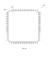
- FIG. 1A is a top plan view of a semiconductor package constructed in accordance with a first embodiment of the present invention
- FIG. 1B is a bottom plan view of the semiconductor package shown in FIG. 1A ;
- FIG. 1C is a cross-sectional view taken along line 1 C- 1 C of FIG. 1B ;
- FIG. 1D is a top plan view of an unsingulated leadframe which is integrated into the semiconductor package shown in FIGS. 1A-1C ;
- FIG. 2 is a flow chart illustrating an exemplary fabrication method for the semiconductor package shown in FIGS. 1A-1C ;
- FIGS. 3A-3I are views illustrating an exemplary fabrication method for the semiconductor package shown in FIGS. 1A-1C ;
- FIG. 4A is a top plan view of a semiconductor package constructed in accordance with a second embodiment of the present invention.
- FIG. 4B is a bottom plan view of the semiconductor package shown in FIG. 4A ;
- FIG. 4C is a cross-sectional view taken along line 4 C- 4 C of FIG. 4B ;
- FIG. 4D is a top plan view of an unsingulated leadframe which is integrated into the semiconductor package shown in FIGS. 4A-4C ;
- FIG. 5A is a top plan view of a semiconductor package constructed in accordance with a third embodiment of the present invention.
- FIG. 5B is a bottom plan view of the semiconductor package shown in FIG. 5A ;
- FIG. 5C is a cross-sectional view taken along line 5 C- 5 C of FIG. 5B ;
- FIG. 5D is a top plan view of an unsingulated leadframe which is integrated into the semiconductor package shown in FIGS. 5A-5C ;
- FIG. 6A is a top plan view of a semiconductor package constructed in accordance with a fourth embodiment of the present invention.
- FIG. 6B is a cross-sectional view taken along line 6 B- 6 B of FIG. 6A ;
- FIG. 6C is a bottom plan view of an unsingulated leadframe which is integrated into the semiconductor package shown in FIGS. 6A and 6B , further illustrating a semiconductor die as attached to the leadframe;
- FIG. 7 is a cross-sectional view of a semiconductor package constructed in accordance with a fifth embodiment of the present invention.
- FIG. 8 is a flow chart illustrating an exemplary fabrication method for the semiconductor package shown in FIG. 7 ;
- FIGS. 9A-9E are views illustrating an exemplary fabrication method for the semiconductor package shown in FIG. 7 ;
- FIG. 10 is a partial cut-away perspective view of the semiconductor package shown in FIG. 7 , illustrating an exemplary connection between first and second semiconductor devices of the semiconductor package;
- FIG. 11 is an enlargement of the encircled region 11 included in FIG. 10 ;
- FIG. 12 is a cross-sectional view of a semiconductor package constructed in accordance with a sixth embodiment of the present invention.
- FIG. 13 is a cross-sectional view of a semiconductor package constructed in accordance with a seventh embodiment of the present invention.
- FIG. 14 is a cross-sectional view of a semiconductor package constructed in accordance with an eighth embodiment of the present invention.
- FIGS. 1A-1C depict a semiconductor package 200 constructed in accordance with a first embodiment of the present invention.
- the leadframe 100 integrated into the semiconductor package 200 is shown in its unsingulated state in FIG. 1D .
- the leadframe 100 comprises a generally quadrangular (e.g., square) die pad 110 which defines four peripheral edge segments.
- the die pad 110 of the leadframe 100 is not of uniform thickness. Rather, formed in a peripheral portion of the bottom surface of the die pad 110 is a half-etched portion 111 . More particularly, the half-etched portion 111 is segregated into four segments, with each of these segments extending along a respective one of peripheral edge segments of the die pad 110 and between a respective pair of tie bars 120 of the leadframe 100 which are described in more detail below. Though FIG.
- FIG. 1D is a top perspective view of the leadframe 100 , the half-etched portion 111 in the bottom surface of the die pad 110 is indicated by the condensed hatching shown in FIG. 1D .
- a semiconductor die is attached to the top surface of the die pad 110 through the use of an adhesive layer, with an encapsulant material thereafter being applied to the semiconductor die and the leadframe 100 to form the package body of the semiconductor package 200 .
- the half-etched portion 111 formed in the peripheral portion of the bottom surface of the die pad 110 as indicated above effectively increases the distance along which moisture must travel to reach the semiconductor die mounted to the top surface of the die pad 110 .
- the flow of encapsulant material over the half-etched portion 111 during the formation of the package body of the semiconductor package 200 facilitates the creation of a mechanical interlock between the package body and the die pad 110 .
- the leadframe 100 includes four tie bars 120 which extend diagonally from respective ones of the four corner regions defined by the die pad 110 .
- the tie bars 120 are integrally connected to a generally quadrangular dambar 130 which circumvents the die pad 110 and is disposed in spaced relation thereto.
- each of the tie bars 120 is bent to include a first downset 121 and a second downset 122 . The first downset 121 of each tie bar 120 is disposed between the second downset 122 and the die pad 110 .
- each of the tie bars 120 includes a first segment which is disposed between the die pad 110 and the first downset 131 and extends in generally co-planar relation to the die pad 110 , a second segment which extends between the first and second downsets 121 , 122 and resides on a plane which is elevated above that of the die pad 110 , and a third segment which extends between the second downset 122 and the dambar 130 and resides on a plane which is elevated above that of the second segment.
- each tie bar 120 reside on respective ones of three spaced, generally parallel planes, with the plane upon which the second segment resides being disposed between those planes on which respective ones of the first and third segments reside.
- the die pad 110 resides on the first plane, with the dambar 130 residing on the third plane.
- each of the tie bars 120 may be provided with a first opposed pair of integral locking protrusions to assist in the mechanical interlock of the tie bars 120 to the package body of the semiconductor package 200 .
- each of the tie bars 120 may include a second opposed pair of locking protrusions which are integrally connected to the die pad 110 .
- Each of the locking protrusions of the second pair may be half etched, with the etched surface defining the bottom surface thereof.
- the encapsulant material used to form the package body of the semiconductor package 200 is also able to flow over the etched bottom surfaces of the locking protrusions of the second pair, as well as the third segments including the locking protrusions of the first pair thereon, thus resulting in portions of the tie bars 120 being encapsulated by the package body of the semiconductor package 200 which improves the bonding or mechanical interlock therebetween.
- the etched surfaces of the locking protrusions of the second pair are also indicated by the hatching shown in FIG. 1D , such etched bottom surfaces extending in generally co-planar relation to the half-etched portion 111 of the die pad 110 .
- the semiconductor die overlaps an inner end portion 124 of the top surface of each tie bar 120 , such inner end portion being shown by the less condensed hatching included in FIG. 1D .
- the semiconductor die also overlaps portions of the top surfaces of each of the locking protrusions of the second pair of each tie bar 120 .
- the tie bars 120 are integrally connected to the dambar 130 which circumvents the die pad 110 .
- the dambar 130 is provided in the form of a substantially quadrangular (e.g., square) ring which interconnects the distal ends of the tie bars 120 , thus resulting in the dambar 130 extending in generally co-planar relation to the third segments of the tie bars 120 . More particularly, as best seen in FIG. 1D , the dambar 130 defines four peripheral segments which extend in spaced, generally parallel relation to respective ones of the peripheral edge segments of the die pad 110 .
- the dambar 130 is singulated or removed from the leadframe 100 to electrically isolate other structural features of the leadframe 100 from each other.
- the leadframe 100 of the semiconductor package 200 further comprises a plurality of first leads 140 which are integrally connected to the dambar 130 and extend inwardly toward the die pad 110 . More particularly, the first leads 140 are segregated into four sets, with the first leads 140 of each set being integrally connected to an extending generally perpendicularly from a respective one of the four peripheral segments defined by the dambar 130 . The first leads 140 of each set are also arranged at a predetermined pitch and are each of a predetermined length. As is apparent from FIG. 1D , the first leads 140 are not in electrical contact with the die pad 110 . Rather, the distal end of each of the first leads 140 is positioned in spaced relation to the die pad 110 .
- each of the first leads 140 is bent to include a first downset 141 and a second downset 142 .
- the first downset 141 of each first lead 140 is disposed between the second downset 142 and the die pad 110 .
- each of the first leads 140 includes a first segment which is disposed between the die pad 110 and the first downset 141 and extends in generally co-planar relation to the die pad 110 , a second segment which extends between the first and second downsets 141 , 142 and resides on a plane which is elevated above that of the die pad 110 , and a third segment which extends between the second downset 142 and the dambar 130 and resides on a plane which is elevated above that of the second segment.
- each first lead 140 reside on respective ones of three spaced, generally parallel planes, with the plane upon which the second segment resides being disposed between those planes on which respective ones of the first and third segments reside.
- the die pad 110 and the first segments of the tie bars 120 reside on the first plane, with the second segments of the tie bars 120 residing on the second plane, and the dambar 130 and the third segments of the tie bars 120 residing on the third plane.
- the semiconductor die overlaps an inner end portion of the top surface of the first segment of each first lead 140 .
- formed in the bottom surface of the first segment of each first lead 140 is a half-etched portion 144 which is disposed in opposed relation to the inner end portion defined by the top surface thereof.
- the half-etched portion 144 of each first lead 140 defines the bottom surface of the inner end portion thereof.
- FIG. 1D is a top plan view of the leadframe 100
- the half-etched portion 144 of each first lead 140 is indicated by the condensed hatching shown in FIG. 1D .
- the half-etched portion 144 extends to the inner, distal end of the first lead 150 defined by the first segment thereof.
- the non-etched portion of the bottom surface of the first segment of each first lead 140 extending to the first downset 141 defines a generally planar land 145 .
- the land 145 defined by each first lead 140 extends in generally co-planar relation to the generally planar bottom surface of the die pad 110 which is circumvented by the half-etched portion 111 .
- the generally planar top surface of the first segment of each first lead 140 extends in generally co-planar relation to the generally planar top surface of the die pad 110 .
- the half-etched portion 144 of the first segment of each first lead 140 may extend in generally co-planar relation to the half-etched portion 111 of the die pad 110 .
- the half-etched portion 144 of each of the first leads 140 can be formed by either half-etching as described above, or alternatively by forging.
- the encapsulant material used to form the package body of the semiconductor package 200 is able to flow over the half-etched portion 144 , thus facilitating a strong mechanical bond or interlock between each of the first leads 140 and the package body despite the land 145 defined by each first lead 140 being exposed in such package body.
- each first lead 140 also serves to prevent insufficient filling or complete separation of the package body in the vicinity of the lands 145 , and further serves to fix the first leads 140 within the package body such that the lands 145 do not protrude from the bottom surface of the package body, but rather are substantially flush or continuous therewith as will be described in more detail below.
- each of the first leads 140 may further include a notch cut 147 disposed in the bottom surface at that end of the land 145 opposite that extending to the half-etched portion 144 .
- the notch cut 147 is formed at the bent portion of the first lead 140 where the first downset 141 and the land 145 meet.
- the notch cuts 147 prevent the occurrence of rolling over at the bent portions during formation of the first downsets 141 .
- the package body of the semiconductor package 200 including the leadframe 100 is protected from being broken at the bent portions, and the lands 145 are protected from being irregularly deformed, thus enabling stable mounting of the semiconductor package on an underlying structure such as a printed circuit board (PCB).
- PCB printed circuit board
- each of the first leads 140 further includes a wire bonding area 146 defined by the top surface of the second segment thereof which, as indicated above, extends between the first and second downsets 141 , 142 .
- the wire bonding area 146 is situated at a higher level than the die pad 110 .
- the wire bonding area 146 of each of the first leads 140 provides an area for the electrical bonding of conductive wires.
- the leadframe 100 constructed in accordance with the present invention further comprises a plurality of second leads 150 which are integrally connected to the dambar 130 .
- the second leads 150 like the first leads 140 , are preferably segregated into four sets, with each set of the second leads 150 extending between an adjacent pair of the tie bars 120 .
- the second leads 150 of each set also extend generally perpendicularly relative to a respective one of the peripheral segments of the dambar 130 at a predetermined length, the second leads 150 of each set also being arranged at a predetermined pitch.
- Each of the second leads 150 includes an inner portion 152 which extends extend inwardly from the dambar 130 toward the die pad 110 in spaced relation thereto.
- each of the second leads 150 includes an outer portion 160 which extends extend outwardly from the dambar 130 away from the die pad 110 .
- the outer portions 160 are preferably linearly aligned with respective ones of the inner portions 152 .
- the inner portions 152 are shorter in length than the first leads 140 .
- certain ones of the inner portions 152 of each set of the second leads 150 have a generally linear configuration, and extend between a respective, adjacent pair of the first leads 140 in spaced relation thereto.
- Those inner portions 152 of each set of the second leads 150 which do not extend between an adjacent pair of the first leads 140 each preferably have an angled configuration so as to be disposed closer to a respective one of the peripheral edge segments of the die pad 110 .
- each of the inner portions 152 which has a generally straight or linear configuration and extends between an adjacent pair of the first leads 140 is preferably bent to include a downset 151 . Due to the inclusion of the downset 151 therein, each of the inner portions 152 includes a first segment which is disposed between the downset 151 and the die pad 110 , and a second segment which extends between the downset 151 and the dambar 130 .
- the first segments of the inner portions 152 preferably reside on the same plane as the second segments of the first leads 140 .
- the second segments of the inner portions 152 preferably reside on the same plane as the third segments of the first leads 140 and the dambar 130 .
- each of the inner portions 152 includes a wire bonding area 156 which is defined by the top surface of the first segment thereof and extends from the downset 151 to the distal end of the inner portion 152 defined by the first segment.
- the wire bonding areas 156 of the inner portions 152 extend in generally co-planar relation to the wire bonding areas 146 of the first leads 140 .
- the wire bonding areas 156 of the inner portions 152 of the second leads 150 provide areas for the electrical bonding of conductive wires, as will be described in more detail below.
- gold or silver may be plated on the wire bonding areas 146 , 156 .
- the leadframe 100 may a pre-plated leadframe (PPF) to provide enhanced wire bonding areas.
- PPF pre-plated leadframe
- the outer portions 160 of the second leads 150 , the dambar 130 , the second segments of the inner portions 152 of the second leads 150 , and the third segments of the first leads 140 all reside on a common plane.
- the dambar 130 is ultimately singulated in a manner wherein each outer portion 160 remains integrally connected to a respective one of the inner portions 152 , with each connected pair of the inner and outer portions 152 , 160 (and thus each second lead 150 ) being electrically isolated from every other second lead 150 .
- the singulation of the dambar 130 also occurs in a manner wherein the first leads 140 are electrically isolated from each other, and from each second lead 150 .
- the leadframe 100 of the semiconductor package 200 may be fabricated from a conventional metal material, such as copper, copper alloy, steel plated with copper, or a functional equivalent. However, those of ordinary skill in the art will recognize that the present invention is not limited to any particular material for the leadframe 100 . Additionally, the number of first and second leads 140 , 150 shown in FIG. 1D is for illustrative purposes only, and may be modified according to application field. Along these lines, the first and second leads 140 , 150 may have designs or configurations varying from those shown in FIG. 1D without departing from the spirit and scope of the present invention.
- first and second leads 140 , 150 are each shown as each being segregated into four sets, it will be recognized that fewer sets of the first and second leads 140 , 150 may be provided, and may be arranged along any combination of two or three of the peripheral sides of the die pad 110 . Moreover, less than four tie bars 120 may be included in the leadframe 100 , extending to respective corners of the die pad 110 in any combination. It is further contemplated that the leadframe 100 may be fabricated through the implementation of a chemical etching process or alternatively a mechanical stamping process.
- the dambar 130 is singulated or removed from the leadframe 100 to facilitate the electrical isolation of the various structural features of the leadframe 100 from each other. More particularly, the dambar 130 is singulated in a manner wherein each outer portion 160 remains integrally connected to a respective one of the inner portions 152 , and the second leads 150 are electrically isolated from each other. The singulation of the dambar 130 also occurs in a manner wherein the first leads 140 are electrically isolated from each other, and from each of the second leads 150 .
- a semiconductor die 210 is attached to and covers the generally planar top surface of the die pad 110 , the generally planar inner end portions of the top surfaces of the first segments of the first leads 140 , and the inner end portions 124 of the top surfaces of the tie bars 120 .
- Such attachment is preferably facilitated through the use of and of an adhesive layer 201 .
- the semiconductor die 210 directly pushes down on and equally supports the die pad 110 , the inner end portions of the first leads 140 , and the inner end portions 124 of the tie bars 120 .
- the exposed lands 145 of the first leads 140 are effectively stabilized, which ensures their consistent shape and orientation with the semiconductor package 200 .
- the semiconductor die 210 ensures the flatness or co-planarity of the lands 145 . If the lands 145 are not co-planar, a large amount of flash (a portion of the encapsulant used to form the package body of the semiconductor package 200 ) may occur on the lands 145 during the fabrication of the semiconductor package 200 .
- the adhesive layer 201 is preferably a film type adhesive with low moisture absorption that is advantageous in preventing the semiconductor die 210 , the die pad 110 , the inner end portions of the first leads 140 and the inner end portions 124 of the tie bars 120 from being separated from the adhesive layer 201 .
- the semiconductor die 210 includes a plurality of bond pads 211 which are disposed on the top surface thereof opposite the bottom surface adhered to the adhesive layer 201 .
- the bond pads 211 are used to deliver and receive electrical signals.
- the semiconductor package 200 further comprises a plurality of conductive wires 220 which are used to electrically connect the bond pads 211 of the semiconductor die 210 to respective ones of the first leads 140 and the inner portions 152 of the second leads 150 .
- the conductive wires 220 may be fabricated from aluminum, copper, gold, silver, or a functional equivalent. However, those of ordinary skill in the art will recognize that the present invention is not limited to any particular material for the wires 220 .
- the conductive wires 220 in electrically connecting the bond pads 211 to the first leads 140 , it is contemplated that the conductive wires 220 will be extended from the bond pads 211 to the wire bonding areas 146 defined by the second segments of respective ones of the first leads 140 .
- the electrical connection of the bond pads 211 of the semiconductor die 210 to the first leads 140 may also be facilitated by extending the conductive wires 220 between the bond pads 211 and the top surfaces of the first segments of respective ones of the first leads 140 .
- the electrical connection of the bond pads 211 of the semiconductor die 210 to the second leads 150 is preferably facilitated by extending the conductive wires 220 from the bond pads 211 to the wire bonding areas 156 defined by the first segments of respective ones of the inner portions 152 .
- the conductive wires 220 can be bonded to the wire bonding areas 146 , 156 by repeatedly reciprocating capillaries at the same height to maintain constant wiring bonding quality.
- the die pad 110 , the tie bars 120 , the first leads 140 , the inner portions 152 of the second leads 150 , the semiconductor die 210 and the conductive wires 220 are at least partially encapsulated or covered by an encapsulant material which, upon hardening, forms the package body 230 of the semiconductor package 200 . More particularly, the package body 230 covers the entirety of the die pad 210 except for the bottom surface thereof which is circumvented by the half-etched portion 111 . The package body 230 also covers the entirety of each of the first leads 140 except for the land 145 defined thereby and a small portion of the third segment thereof.
- the package body 230 also covers the entirety of each of the inner portions 152 of the second leads 150 except for a small portion of the second segment thereof.
- the entirety of each of the tie bars 120 is also covered by the package body 230 , except for the bottom surface of the first segment of each tie bar 120 which extends in generally co-planar relation to the bottom surface of the die pad 110 and the lands 145 defined by the extension leads 140 .
- the outer portions 160 of the second leads 150 of the leadframe 100 are not covered by the package body 230 .
- the dambar 130 is also not covered by the package body 230 so that it may be removed from the leadframe 100 .
- the generally planar bottom surface of the die pad 110 is exposed in and substantially flush with the generally planar bottom surface 232 of the package body 230 , as are the generally planar bottom surfaces of the first segments of the tie bars 120 .
- the generally planar land 145 defined by each first lead 140 is exposed in and substantially flush with the bottom surface 232 of the package body 230 .
- the outer portions 160 of the second leads 150 of each set thereof protrude laterally outward from respective side surfaces 231 of the package body 230 . As seen in FIGS. 1A-1C , the exposed outer portions 160 may be bent to assume a gull-wing configuration to allow the same to be electrically connected to an underlying substrate such as a printed circuit board.
- the dambar 130 must be removed from the leadframe 100 to facilitate the electrical isolation of the first leads 140 and the second leads 150 from each other as explained above.
- a conventionally known debarring process may be implemented to remove the dambar 130 . The completion of such debarring process results in each of the first leads 140 defining an outer, distal end which is exposed in and substantially flush with a respective side surface 231 defined by the package body 230 .
- the wire bonding areas 146 , 156 to which the conductive wires 220 are extended can prevent sweeping and shorting of the conductive wires 220 arising from the flow of the encapsulant material during the process of forming the package body 230 .
- the semiconductor die 210 directly pushes down on and equally supports the die pad 110 , the inner end portions of the first leads 140 , and the inner end portions 124 of the tie bars 120 .
- the exposed lands 145 of the first leads 140 are effectively stabilized, which ensures their consistent shape and orientation with the semiconductor package 200 .
- the semiconductor package 200 With the configuration of the leadframe 100 described above, a total of about sixty-four (sixteen per side) second leads 150 and a total of about thirty-six (nine per side) lands 145 are included in the lead frame 100 of the semiconductor package 200 . That is, the semiconductor package 200 further has thirty-six I/O pins through the lands 145 . As indicated above, the particular number of I/O pins described above is not intended to limit the present invention.
- the outer portions 160 of the second leads 150 are exposed in the semiconductor package 200 , as are the lands 145 defined by the first leads 140 .
- the lands 145 are capable of being mounted to the surface of an underlying substrate such as a printed circuit board through the use of, for example, a soldering technique. Electrical signals are routed between the lands 145 and the semiconductor die 210 by the corresponding first leads 140 and conductive wires 220 . Similarly, electrical signals may be routed from the semiconductor die 210 to the outer portions 160 by the corresponding integrally connected inner portions 152 and conductive wires 220 .
- the outer portions 160 may be surface mounted to an underlying substrate such as a printed circuit board through the use of, for example, a soldering technique. Since the leadframe 100 of the semiconductor package 200 is configured to provide the outer portions 160 which protrude from the side surfaces 231 of the package body 230 and the lands 145 which are exposed in the bottom surface 232 of the package body 230 , the number of I/O's in the leadframe 100 increases in proportion to the number of the outer portions 160 (i.e., second leads 150 ) and the lands 145 .
- FIG. 2 there is provided a flow chart which sets forth an exemplary method for fabricating the semiconductor package 200 of the present invention.
- the method comprises the steps of preparing the leadframe (S 1 ), semiconductor die attachment (S 2 ), wire bonding (S 3 ), encapsulation (S 4 ), chemical deflashing (S 5 ), trimming (S 6 ), solder plating (S 7 ), marking (S 8 ), and forming and singulation (S 9 ).
- FIGS. 3A-3I provide illustrations corresponding to these particular steps, as will be discussed in more detail below.
- step S 2 is completed wherein the semiconductor die 210 having the bond pads 211 is attached to and covers the generally planar top surface of the die pad 110 , the generally planar inner end portions of the top surfaces of the first segments of the first leads 140 , and the inner end portions 124 of the top surfaces of the tie bars 120 through the use of the adhesive layer 201 .
- the adhesive layer 201 can be selected from well known liquid epoxy adhesives, adhesive films and adhesive tapes, as well as equivalents thereto.
- the conductive wires 220 are used to electrically interconnect the semiconductor die 210 to the leadframe 100 in the aforementioned manner. Specifically, the bond pads 211 of the semiconductor die 210 are electrically connected to the first leads 140 and the second leads 150 .
- portions of the leadframe 100 , the semiconductor die 210 and the conductive wires 220 are encapsulated with an encapsulant material which, upon hardening, forms the package body 230 of the semiconductor package 200 .
- the package body 230 covers the entirety of the die pad 210 except for the bottom surface thereof which is circumvented by the half-etched portion 111 .
- the package body 230 also covers the entirety of each of the first leads 140 except for the land 145 defined thereby and a small portion of the third segment thereof.
- the package body 230 also covers the entirety of each of the inner portions 152 of the second leads 150 except for a small portion of the second segment thereof.
- each of the tie bars 120 is also covered by the package body 230 , except for the bottom surface of the first segment of each tie bar 120 which extends in generally co-planar relation to the bottom surface of the die pad 110 and the lands 145 defined by the first leads 140 .
- the outer portions 160 of the second leads 150 of the leadframe 100 are not covered by the package body 230 .
- the dambar 130 is also not covered by the package body 230 so that it may be removed from the leadframe 100 .
- step S 5 chemical deflashing may be performed if films of flash (a resin component of the encapsulant material) are formed on the bottom surface of the die pad 110 and upon the lands 145 . If such thin films of flash are present as could impede the ability to mount the semiconductor package 200 to an underlying substrate, the removal of such flash films by a chemical etching method is required.
- the dambar 130 is trimmed or removed by cutting so that the first leads 140 and the second leads 150 are electrically isolated from each other in the above described manner.
- the dambar 130 is positioned outside of the package body 230 to allow for the removal thereof from the leadframe 100 , and is removed by cutting the same with dambar cutting tools 149 .
- portions of the first leads 140 protruding from the side surfaces 231 of the package body 230 are also completely removed during the trimming process.
- a solder plating step (step S 7 ) may also be performed in the fabrication process for the semiconductor package 200 . More particularly, after the dambar 130 and portions of the first leads 140 have been removed using the dambar cutting tools 149 , some metal areas of the leadframe 100 susceptible to oxidation are exposed to air. Since the leadframe 100 is typically made of copper, the same is susceptible to oxidation. In order to prevent the oxidation of the exposed metal areas of the leadframe 100 , all elements (e.g. the first leads 140 ) of the leadframe 100 exposed outside of the package body 230 may be plated by soldering.
- a marking step may be performed upon the semiconductor package 200 . More particularly, ink or a laser may be used to mark the product name, the manufacturer of the semiconductor package 200 , etc. on a prescribed surface of the package body 230 .
- the outer portions 160 of the second leads 150 protruding from the package body 230 are formed in appropriate shapes.
- the exposed outer portions 160 protruding from the side surfaces 231 of the package body 230 may be formed into predetermined shapes using a lead forming tool (not shown) to allow the semiconductor package 200 to have a shape suitable for mounting to an external unit or an underlying substrate.
- the outer portions 160 are depicted as being formed outwardly relative to the package body 230 in FIG. 3I , those of ordinary skill in the art will recognize that the outer portions 160 can alternatively be formed downwardly and inwardly relative to the package body 230 .
- portions of the tie bars 120 protruding outwardly from the package body 230 are cut to separate the semiconductor package 200 from the leadframe 100 .
- FIGS. 4A-4C there is shown a semiconductor package 400 constructed in accordance with a second embodiment of the present invention.
- the leadframe 300 integrated into the semiconductor package 400 is shown in its unsingulated state in FIG. 4D .
- the leadframe 300 comprises a generally quadrangular (e.g., square) die pad 310 which defines four peripheral edge segments.
- the die pad 310 of the leadframe 300 is not of uniform thickness. Rather, formed in a peripheral portion of the bottom surface of the die pad 310 is a half-etched portion 311 . More particularly, the half-etched portion 311 is segregated into four segments, with each of these segments extending along a respective one of peripheral edge segments of the die pad 310 and between a respective pair of tie bars 320 of the leadframe 300 which are described in more detail below. Though FIG.
- FIG. 4D is a top plan view of the leadframe 300 , the half-etched portion 311 in the bottom surface of the die pad 310 is indicated by the condensed hatching shown in FIG. 4D .
- the half-etched portion 311 provides the same functionality described above in relation to the half-etched portion 111 of the die pad 110 included in the leadframe 100 .
- the leadframe 300 includes four tie bars 320 which extend diagonally from respective ones of the four corner regions defined by the die pad 310 .
- the tie bars 320 are integrally connected to a generally quadrangular dambar 330 which circumvents the die pad 310 and is disposed in spaced relation thereto.
- each of the tie bars 320 is bent to include a first downset 321 and a second downset 322 . The first downset 321 of each tie bar 320 is disposed between the second downset 322 and the die pad 310 .
- each of the tie bars 320 includes a first segment which is disposed between the die pad 310 and the first downset 331 and extends in generally co-planar relation to the die pad 310 , a second segment which extends between the first and second downsets 321 , 322 and resides on a plane which is elevated above that of the die pad 310 , and a third segment which extends between the second downset 322 and the dambar 330 and resides on a plane which is elevated above that of the second segment.
- each tie bar 320 reside on respective ones of three spaced, generally parallel planes, with the plane upon which the second segment resides being disposed between those planes on which respective ones of the first and third segments reside.
- the die pad 310 resides on the first plane, with the dambar 330 residing on the third plane.
- each of the tie bars 320 may be provided with a first opposed pair of integral locking protrusions to assist in the mechanical interlock of the tie bars 320 to the package body of the semiconductor package 400 .
- each of the tie bars 320 may include a second opposed pair of locking protrusions which are integrally connected to the die pad 310 .
- Each of the locking protrusions of the second pair may be half etched, with the etched surface defining the bottom surface thereof.
- the encapsulant material used to form the package body of the semiconductor package 400 is also able to flow over the etched bottom surfaces of the locking protrusions of the second pair, as well as the third segments including the locking protrusions of the first pair thereon, thus resulting in portions of the tie bars 320 being encapsulated by the package body of the semiconductor package 400 which improves the bonding or mechanical interlock therebetween.
- the etched surfaces of the locking protrusions of the second pair are also indicated by the hatching shown in FIG. 4D , such etched bottom surfaces extending in generally co-planar relation to the half-etched portion 311 of the die pad 310 .
- the semiconductor die overlaps an inner end portion 324 of the top surface of each tie bar 320 , such inner end portion being shown by the less condensed hatching included in FIG. 4D .
- the semiconductor die also overlaps portions of the top surfaces of each of the locking protrusions of the second pair of each tie bar 320 .
- the tie bars 320 are integrally connected to the dambar 330 which circumvents the die pad 310 .
- the dambar 330 is provided in the form of a substantially quadrangular (e.g., square) ring which interconnects the distal ends of the tie bars 320 , thus resulting in the dambar 330 extending in generally co-planar relation to the third segments of the tie bars 320 . More particularly, as best seen in FIG. 4D , the dambar 330 defines four peripheral segments which extend in spaced, generally parallel relation to respective ones of the peripheral edge segments of the die pad 310 . In the completed semiconductor package 400 , the dambar 330 is singulated or removed from the leadframe 300 to electrically isolate other structural features of the leadframe 300 from each other.
- each of the tie bars 320 is integrally connected to the dambar 330 .
- each of the tie bars 320 is integrally connected to a land connecting bar 340 which, like the dambar 330 , circumvents the die pad 310 .
- the land connecting bar 340 includes four peripheral segments which extend in spaced, generally parallel relation to respective ones of the peripheral edge segments of the die pad 310 .
- the land connecting bar 340 is concentrically positioned between the dambar 330 and the die pad 310 , and is integrally connected to the tie bars 320 between the die pad 310 and the first downsets 321 of the tie bars 320 . As seen in FIG.
- each of the peripheral segments of the land connecting bar 340 includes a pair of chamfer portions which define the junctions with respective ones of the tie bars 320 of the pair between which such peripheral segment extends.
- Each chamfer portion is formed to extend at a predetermined angle relative the remainder of the peripheral segment upon which it is included, and further extends generally perpendicularly relative to the tie bar 320 to which it is integrally connected. The use of the chamfer portions of the land connecting bar 340 will be discussed in more detail below.
- the leadframe 300 further comprises a plurality of first leads 360 which are each integrally connected to the land connecting bar 340 , and protrude inwardly toward the die pad 310 . More particularly, as best seen in FIG. 4D , the first leads 360 are segregated into four sets, with each set of the first leads 360 protruding inwardly from a respective one of the peripheral segments of the land connecting bar 340 toward the die pad 310 . The first leads 360 of each set are arrange at a predetermined pitch and protrude perpendicularly inward at a predetermined length from a respective one of the peripheral segments of the land connecting bar 340 .
- Each of the first leads 360 has a generally planar top surface which extends in generally co-planar relation to the top surface of the die pad 310 , and a generally planar bottom surface which extends in generally co-planar relation to the bottom surface of the die pad 310 and defines a land 365 .
- the top surface of each first lead 360 defines a wire bonding area 366 thereof.
- each first lead 360 overlaps an inner end portion of the top surface of each first lead 360 .
- a half-etched portion 364 which is disposed in opposed relation to the inner end portion defined by the top surface or wire bonding area 366 thereof.
- the half-etched portion 364 of each first lead 360 defines the bottom surface of the inner end portion thereof.
- FIG. 4D is a top perspective view of the leadframe 300
- the half-etched portion 364 of each first lead 360 is indicated by the condensed hatching shown in FIG. 4D .
- the half-etched portion 364 extends between the land 365 and the inner, distal end of the first lead 360 .
- each first lead 360 extends in generally co-planar relation to the generally planar bottom surface of the die pad 310 which is circumvented by the half-etched portion 311 .
- the generally planar top surface of each first lead 360 extends in generally co-planar relation to the generally planar top surface of the die pad 310 .
- the half-etched portion 364 of each first lead 360 may extend in generally co-planar relation to the half-etched portion 311 of the die pad 310 .
- the half-etched portion 364 of each of the first leads 360 can be formed by either half-etching as described above, or alternatively by forging.
- the encapsulant material used to form the package body of the semiconductor package 400 is able to flow over the half-etched portions 364 , thus facilitating a strong mechanical bond or interlock between each of the first leads 360 and the package body despite the lands 365 being exposed in such package body.
- This mechanical interlock assists in preventing the first leads 360 from being dislodged from the package body during a subsequent sawing process involved in the fabrication of the semiconductor package 400 , as will also be described in more detail below.
- each first lead 360 also serves to prevent insufficient filling or complete separation of the package body in the vicinity of the lands 365 , and further serves to fix the first leads 360 within the package body such that the lands 365 do not protrude from the bottom surface of the package body, but rather are substantially flush or continuous therewith as will be described in more detail below.
- the leadframe 300 of the semiconductor package 400 further comprises a plurality of second leads 350 which are integrally connected to the land connecting bar 340 and extend outwardly toward the dambar 330 .
- the second leads 350 are segregated into four sets, with the second leads 350 of each set being integrally connected to and extending generally perpendicularly outward from a respective one of the four peripheral segments defined by the land connecting bar 340 .
- the second leads 350 of each set are arrange at a predetermined pitch and protrude perpendicularly outward at a predetermined length from a respective one of the peripheral segments of the land connecting bar 340 .
- the second leads 350 are each integrally connected to the dambar 330 .
- the second leads 350 of each set extend generally perpendicularly between a corresponding pair of the peripheral segments of the land connecting bar 340 and dambar 330 .
- each of the second leads 350 is bent to include a first downset 351 and a second downset 352 .
- the first downset 351 of each second lead 350 is disposed between the second downset 352 and the land connecting bar 340 .
- each of the second leads 350 includes a first segment which is disposed between the land connecting bar 340 and the first downset 351 and extends in generally co-planar relation to the die pad 310 and first leads 360 , a second segment which extends between the first and second downsets 351 , 352 and resides on a plane which is elevated above that of the die pad 310 , and a third segment which extends between the second downset 352 and the dambar 330 and resides on a plane which is elevated above that of the second segment.
- each second lead 350 reside on respective ones of three spaced, generally parallel planes, with the plane upon which the second segment resides being disposed between those planes on which respective ones of the first and third segments reside.
- the die pad 310 , the land connecting bar 340 , the first leads 360 , and the first segments of the tie bars 320 reside on the first plane, with the second segments of the tie bars 320 residing on the second plane, and the dambar 330 and the third segments of the tie bars 320 residing on the third plane.
- the generally planar bottom surface of the first segment of each second lead 350 defines a land 355 .
- the land 355 defined by each second lead 350 extends in generally co-planar relation to the generally planar bottom surface of the die pad 310 which is circumvented by the half-etched portion 311 , and further extends in generally co-planar relation to the land 365 defined by each first lead 360 .
- the first segment of each second lead 350 further defines a generally planar top surface which extends in generally co-planar relation to the generally planar top surface of the die pad 310 , and also to the generally planar top surfaces of the first leads 360 .
- the third segment of each second lead 350 extends in generally co-planar relation to the dambar 330 . As best seen in FIG.
- the lands 365 defined by the first leads 360 of each set are linearly aligned with respective ones of the lands 355 defined by the second leads 350 of the corresponding set, the lands 355 , 365 each being exposed in and substantially flush with an exterior surface defined by the package body of the semiconductor package 400 so as to be electrically connectable to an underlying substrate such as a printed circuit board.
- each of the second leads 350 further includes a wire bonding area 356 defined by the top surface of the second segment thereof which, as indicated above, extends between the first and second downsets 351 , 352 .
- the wire bonding area 356 is situated at a higher level than the die pad 310 .
- the wire bonding area 356 of each of the second leads 350 provides an area for the electrical bonding of conductive wires.
- each of the second leads 350 may further include a notch cut 357 disposed at the bent portion of the second lead 350 where the first downset 351 and the land 355 meet.
- the notch cuts 357 prevent the occurrence of rolling over at the bent portions during formation of the first downsets 351 .
- the package body of the semiconductor package 400 including the leadframe 300 is protected from being broken at the bent portions, and the lands 355 are protected from being irregularly deformed, thus enabling stable mounting of the semiconductor package on an underlying structure such as a printed circuit board (PCB).
- PCB printed circuit board
- the leadframe 300 constructed in accordance with the present invention further comprises a plurality of third leads 370 which are integrally connected to the dambar 330 .
- the third leads 370 like the second leads 350 , are preferably segregated into four sets, with each set of the third leads 370 extending between an adjacent pair of the tie bars 320 .
- the third leads 370 of each set also extend generally perpendicularly relative to a respective one of the peripheral segments of the dambar 330 at a predetermined length, the third leads 370 of each set also being arranged at a predetermined pitch.
- Each of the third leads 370 includes an inner portion 372 which extends extend inwardly from the dambar 330 toward the die pad 310 in spaced relation thereto.
- each of the third leads 370 includes an outer portion 380 which extends extend outwardly from the dambar 330 away from the die pad 310 .
- the outer portions 380 are preferably linearly aligned with respective ones of the inner portions 372 .
- the inner portions 372 are shorter in length than the second leads 350 .
- certain ones of the inner portions 372 of each set of the third leads 370 have a generally linear configuration, and extend between a respective, adjacent pair of the second leads 350 in spaced relation thereto.
- Those inner portions 372 of each set of the third leads 370 which do not extend between an adjacent pair of the second leads 350 each preferably have an angled configuration so as to be disposed closer to a respective one of the peripheral edge segments of the die pad 310 .
- each of the inner portions 372 which has a generally straight or linear configuration and extends between an adjacent pair of the second leads 350 is preferably bent to include a downset 371 . Due to the inclusion of the downset 371 therein, each of the inner portions 372 includes a first segment which is disposed between the downset 371 and the die pad 310 , and a second segment which extends between the downset 371 and the dambar 330 .
- the first segments of the inner portions 372 preferably reside on the same plane as the second segments of the second leads 350 .
- the second segments of the inner portions 372 preferably reside on the same plane as the third segments of the second leads 350 and the dambar 330 .
- each of the inner portions 372 includes a wire bonding area 376 which is defined by the top surface of the first segment thereof and extends from the downset 371 to the distal end of the inner portion 372 defined by the first segment.
- the wire bonding areas 376 of the inner portions 372 extend in generally co-planar relation to the wire bonding areas 356 of the second leads 350 .
- the wire bonding areas 376 of the inner portions 372 of the third leads 370 provide areas for the electrical bonding of conductive wires, as will be described in more detail below.
- the leadframe 100 it is contemplated that for ease of wire bonding, gold or silver may be plated on the wire bonding areas 146 , 156 .
- the leadframe 100 may a pre-plated leadframe (PPF) to provide enhanced wire bonding areas.
- PPF pre-plated leadframe
- the leadframe 300 it is contemplated that for ease of wire bonding, gold or silver may be plated on the wire bonding areas 366 , 356 , 376 .
- the leadframe 300 may a pre-plated leadframe (PPF) to provide enhanced wire bonding areas.
- the outer portions 380 of the third leads 370 , the dambar 330 , the second segments of the inner portions 372 of the third leads 370 , and the third segments of the second leads 350 all reside on a common plane.
- the dambar 330 is ultimately singulated in a manner wherein each outer portion 380 remains integrally connected to a respective one of the inner portions 372 , with each connected pair of the inner and outer portions 372 , 380 (and thus each third lead 370 ) being electrically isolated from every other third lead 370 .
- the singulation of the dambar 330 also occurs in a manner wherein the second leads 350 are electrically isolated from each other, and from the third leads 370 .
- the leadframe 300 of the semiconductor package 400 may be fabricated from a conventional metal material, such as copper, copper alloy, steel plated with copper, or a functional equivalent. However, those of ordinary skill in the art will recognize that the present invention is not limited to any particular material for the leadframe 300 . Additionally, the number of first, second and third leads 360 , 350 , 370 shown in FIG. 4D is for illustrative purposes only, and may be modified according to application field. Along these lines, the first, second and third leads 360 , 350 , 370 may have designs or configurations varying from those shown in FIG. 4D without departing from the spirit and scope of the present invention.
- first, second and third leads 360 , 350 , 370 are each shown as each being segregated into four sets, it will be recognized that fewer sets thereof may be provided, and may be arranged along any combination of two or three of the peripheral sides of the die pad 310 . Moreover, less than four tie bars 320 may be included in the leadframe 300 , extending to respective corners of the die pad 310 in any combination. It is further contemplated that the leadframe 300 may be fabricated through the implementation of a chemical etching process or alternatively a mechanical stamping process.
- the semiconductor package 400 as fabricated to include the leadframe 300 is shown in detail.
- the dambar 330 and the land connecting bar 340 are each singulated or removed from the leadframe 300 to facilitate the electrical isolation of the various structural features of the leadframe 300 from each other. More particularly, the dambar 330 and the land connecting bar 340 are singulated in a manner wherein each outer portion 380 remains integrally connected to a respective one of the inner portions 370 , with the third leads 370 further being electrically isolated from each other.
- the singulation of the dambar 330 and the land connecting bar 340 also occur in a manner wherein the second leads 350 are electrically isolated from each other, from the first leads 360 and from the third leads 370 , with the first leads 360 being electrically isolated from each other, from the second leads 350 and from the third leads 370 .
- a semiconductor die 410 is attached to and covers the generally planar top surface of the die pad 310 , the generally planar inner end portions of the top surfaces of the first leads 360 , and the inner end portions 324 of the top surfaces of the tie bars 320 .
- Such attachment is preferably facilitated through the use of an adhesive layer 401 .
- the semiconductor die 410 Prior to the removal of the land connecting bar 340 , the semiconductor die 410 directly pushes down on and equally supports the die pad 310 , the inner end portions of the first leads 360 (and hence the second leads 350 which are also connected to the land connecting bar 340 ), and the inner end portions 324 of the tie bars 320 .
- the exposed lands 365 of the first leads 360 and the exposed lands 355 of the second leads 350 are effectively stabilized, which ensures their consistent shape and orientation with the semiconductor package 400 .
- the semiconductor die 410 ensures the flatness or co-planarity of the lands 365 , 355 . If the lands 365 , 355 are not co-planar, a large amount of flash (a portion of the encapsulant used to form the package body of the semiconductor package 400 ) may occur on the lands 365 , 355 during the fabrication of the semiconductor package 400 .
- the adhesive layer 401 is preferably a film type adhesive possessing the same attributes of the adhesive layer 201 described above in relation to the semiconductor package 200 .
- the semiconductor die 410 includes a plurality of bond pads 411 which are disposed on the top surface thereof opposite the bottom surface adhered to the adhesive layer 201 . The bond pads 411 are used to deliver and receive electrical signals.
- the semiconductor package 400 further comprises a plurality of conductive wires 420 which are used to electrically connect the bond pads 411 of the semiconductor die 410 to respective ones of the first leads 360 , second leads 350 and third leads 370 .
- the conductive wires 420 may be fabricated from aluminum, copper, gold, silver, or a functional equivalent. However, those of ordinary skill in the art will recognize that the present invention is not limited to any particular material for the wires 420 .
- the conductive wires 420 will be extended from the bond pads 411 to the wire bond areas 366 defined by the first leads 360 .
- the conductive wires 420 will be extended from the bond pads 411 to the wire bonding areas 356 defined by the second segments of respective ones of the second leads 350 .
- the electrical connection of the bond pads 411 of the semiconductor die 410 to the second leads 350 may be facilitated by extending the conductive wires 420 between the bond pads 411 and the top surfaces of the first segments of respective ones of the second leads 350 .
- the electrical connection of the bond pads 411 of the semiconductor die 410 to the third leads 370 is preferably facilitated by extending the conductive wires 420 from the bond pads 411 to the wire bonding areas 376 defined by the first segments of respective ones of the inner portions 372 of the third leads 370 . Since the wire bonding areas 356 of the second leads 350 extend in generally co-planar relation to the wire bonding areas 376 of the inner portions 372 of the third leads 370 , the conductive wires 420 can be bonded to the wire bonding areas 356 , 376 by repeatedly reciprocating capillaries at the same height to maintain constant wiring bonding quality.
- the die pad 310 , the first leads 360 , the tie bars 320 , the second leads 350 , the inner portions 372 of the third leads 370 , the semiconductor die 410 and the conductive wires 420 are at least partially encapsulated or covered by an encapsulant material which, upon hardening, forms the package body 430 of the semiconductor package 400 .
- the package body 430 covers the entirety of the die pad 310 except for the bottom surface thereof which is circumvented by the half-etched portion 311 .
- the package body 430 also covers the entirety of each of the first leads 360 except for the land 365 defined thereby, as well as the entirety of each of the second leads 350 except for the land 355 defined thereby and a small portion of the third segment thereof.
- the package body 430 also covers the entirety of each of the inner portions 372 of the third leads 370 except for a small portion of the second segment thereof.
- the entirety of each of the tie bars 320 is also covered by the package body 430 , except for the bottom surface of the first segment of each tie bar 320 which extends in generally co-planar relation to the bottom surface of the die pad 310 and the lands 355 , 365 , all of which are exposed in a generally planar bottom surface 432 defined by the package body 430 .
- the outer portions 380 of the second leads 370 of the leadframe 300 are not covered by the package body 430 , but rather protrude or extend outwardly from respective lateral side surfaces 431 thereof.
- the dambar 330 is also not covered by the package body 430 so that it may be removed from the leadframe 300 .
- the land connecting bar 340 is partially covered by the package body 430 , the bottom surface of the land connecting bar 340 is exposed in the bottom surface 432 so that the land connecting bar 340 , like the dambar 330 , may be removed from the completed semiconductor package 400 as needed to facilitate the electrical isolation of various structural features thereof from each other. More particularly, the removal of the land connecting bar 340 is needed to facilitate the electrical isolation of the first leads 360 from each other, and from the second leads 350 , and further to facilitate the electrical isolation of the second leads 350 from each other. As shown in FIG.
- the removal of the land connecting bar 340 which is typically accomplished through the completion of a partial sawing process subsequent to the formation of the package body 430 , facilitates the formation of a plurality of elongate grooves 440 within the bottom surface 431 of the package body 430 , such grooves 440 extending in generally perpendicular relation to each other, and generally perpendicularly between an opposed pair of the lateral side surfaces 431 of the package body 430 .
- the generally planar bottom surface of the die pad 310 is exposed in and substantially flush with the generally planar bottom surface 432 of the package body 430 , as are the generally planar bottom surfaces of the first segments of the tie bars 320 .
- the generally planar lands 365 , 355 defined by the first and second leads 360 , 350 are exposed in and substantially flush with the bottom surface 432 of the package body 430 .
- the outer portions 380 of the third leads 370 of each set thereof protrude laterally outward from respective side surfaces 431 of the package body 430 . As seen in FIGS.
- the exposed outer portions 380 may be bent to assume a gull-wing configuration to allow the same to be electrically connected to an underlying substrate such as a printed circuit board.
- the dambar 330 and the land connecting bar 340 must each be removed from the leadframe 300 to facilitate the electrical isolation of the first leads 360 , the second leads 350 , and the third leads 370 from each other as explained above.
- a conventionally known debarring process may be implemented to remove the dambar 330 .
- each of the second leads 350 defining an outer, distal end which is exposed in and substantially flush with a respective side surface 431 defined by the package body 430 .
- the removal of the land connecting bar 340 is facilitated by sawing with a blade, the grooves 440 being formed as an artifact of such sawing process.
- the outer portions 380 of the second leads 370 are exposed in the semiconductor package 400 , as are the lands 355 , 365 .
- the lands 355 , 365 are capable of being mounted to the surface of an underlying substrate such as a printed circuit board through the use of, for example, a soldering technique.
- Electrical signals are routed between the lands 355 , 365 and the semiconductor die 410 by the corresponding first and second leads 360 , 350 and conductive wires 420 .
- electrical signals may be routed from the semiconductor die 410 to the outer portions 380 of the second leads 370 by the corresponding integrally connected inner portions 372 and conductive wires 420 .
- the outer portions 380 may be surface mounted to an underlying substrate such as a printed circuit board through the use of, for example, a soldering technique. Since the leadframe 300 of the semiconductor package 400 is configured to provide the outer portions 380 which protrude from the side surfaces 431 of the package body 430 and the lands 355 , 365 which are exposed in the bottom surface 432 of the package body 430 , the number of I/O's in the leadframe 300 increases in proportion to the number of the third leads 370 and the lands 355 , 365 .
- FIGS. 5A-5C there is shown a semiconductor package 400 ′ constructed in accordance with a third embodiment of the present invention.
- the leadframe 300 ′ integrated into the semiconductor package 400 ′ is shown in its unsingulated state in FIG. 5D .
- the semiconductor package 400 ′ bears substantial similarity to the semiconductor package 400 described above. Thus, only the distinctions between the semiconductor packages 400 , 400 ′ will be highlighted below.
- the common structural features of the semiconductor packages 400 , 400 ′ are identified by the same reference numbers in FIGS. 4A-4D and 5 A- 5 D, with those reference numbers used in conjunction with the semiconductor package 400 ′ in FIGS. 5A-5D being accompanied by an apostrophe.
- the leadframe 300 ′ differs from the leadframe 300 by virtue of its inclusion of a plurality of support bars 341 ′ which are integrally connected to and extend between the die pad 310 ′ and the land connecting bar 340 ′.
- the support bars 341 ′ function to connect the die pad 310 ′ to, and to support the die pad 310 ′ within, the interior of the land connecting bar 340 ′.
- the support bars 341 ′ are segregated into four sets, with each set of the support bars 341 ′ extending generally perpendicularly between a respective one of the peripheral edge segments of the die pad 310 ′ and a corresponding peripheral segment of the land connecting bar 340 ′.
- certain ones of the support bars 341 ′ extend between an adjacent pair of the first leads 360 ′, with certain ones of the support bars 341 ′ extending between a first lead 360 ′ and a respective one of the tie bars 320 ′.
- Each of the support bars 341 ′ has a generally planar top surface which extends in generally co-planar relation to the top surface of the die pad 310 ′. As seen in FIG. 5D , each of the support bars 341 ′ is preferably half-etched so as to define a bottom surface which extends in generally co-planar relation to the half-etched portion 311 ′ of the die pad 310 ′. Though FIG. 5D is a top plan view of the leadframe 300 ′, the half-etched surface of each support bar 431 ′ is indicated by the condensed hatching shown in FIG. 5D .
- the encapsulant material used to form the package body 430 ′ of the semiconductor package 400 ′ is able to flow over the bottom surfaces of the support bars 431 ′, and thus completely covers or encapsulates each support bar 431 ′. Such encapsulation of the support bars 431 ′ prevents the same from effecting the connection of the completed semiconductor package 400 ′ to an external circuit.
- each of the first leads 360 ′ being formed to include one or more integral locking protrusions 367 ′ which protrude from one or both sides thereof.
- Each of the locking protrusions 376 ′ is preferably half-etched as indicated by the condensed hatching shown in FIG. 5D such that each locking protrusion 367 ′ defines a generally planar top surface which extends in generally co-planar relation to the top surface of the corresponding first lead 360 ′, and a bottom surface which is recessed relative to the land 365 ′ defined by the corresponding first lead 360 ′.
- 5D is a top plan view of the leadframe 300 ′, the half-etched surface of each locking protrusion 367 ′ is indicated by the condensed hatching included therein.
- the encapsulant material used to form the package body 430 ′ completely covers or encapsulates each locking protrusion 367 ′ to effectively form a mechanical interlock between the first leads 360 ′ and the package body 430 ′. This mechanical interlock assists in preventing the first leads 360 ′ from being dislodged from the package body 430 ′ during the sawing process used to facilitate the removal of the land connecting bar 340 ′.
- a further distinction between the semiconductor packages 400 , 400 ′ lies in only some of the second leads 350 ′ being integrally connected to the dambar 330 ′, with other ones of the second leads 350 ′ terminating so as to be disposed in spaced relation to the dambar 330 ′.
- This is in contrast to the leadframe 300 wherein each of the second leads 350 is integrally connected to the dambar 330 , in addition to being integrally connected to the land connecting bar 340 .
- certain ones of the first segments are the second leads 350 ′ of each set may be linearly aligned with respective ones of the support bars 341 ′ of that set attached to the corresponding peripheral edge segment of the die pad 310 ′.
- FIGS. 6A and 6B there is shown a semiconductor package 600 constructed in accordance with a fourth embodiment of the present invention.
- the leadframe 500 integrated into the semiconductor package 600 is shown in its unsingulated state in FIG. 6C .
- the leadframe 500 integrated into the semiconductor package 600 is identically configured to the above-described unsingulated leadframe 100 which is shown in FIG. 1D and integrated into the semiconductor package 200 .
- the 500 series reference numbers included in FIG. 6C identify structural features of the leadframe 500 corresponding to those identified with the 100 series reference numbers included in FIG. 1D .
- the leadframe 500 includes a die pad 510 which defines a half-etched portion 511 , a plurality of tie bars 520 which integrally connect the die pad 510 to a dambar 530 , a plurality of first leads 540 which are integrally connected to the dambar 530 , and a plurality of second leads 550 which are integrally connected to the dambar 530 .
- the tie bars 520 of the leadframe 500 each include first and second downsets 521 , 522 formed therein.
- each of the first leads 540 is bent to include first and second downsets 541 , 542 , with a wire bonding area 546 being defined between the first and second downsets 541 , 542 .
- Each first lead 540 also defines a land 545 , and includes a half-etched portion 544 and a notch cut 547 formed therein.
- the inner portion 552 of each of the second leads 550 includes a downset 551 formed therein, and defines a wire bonding area 556 .
- the outer portions 560 of the second leads 550 protruding from the side surfaces of the package body of the semiconductor package 600 including the leadframe 500 are bent in a manner differing from the manner in which the outer portions 180 of the leadframe 100 integrated into the semiconductor package 200 are bent, as will be discussed in more detail below.
- a semiconductor die 610 is attached to the generally planar top surface of the die pad 510 . Such attachment is facilitated through the use of an adhesive layer 601 which is preferably a film type adhesive possessing the same attributes of the adhesive layer 201 described above in relation to the semiconductor package 200 .
- the semiconductor die 610 includes a plurality of bond pads 611 which are disposed on the top surface thereof opposite the bottom surface adhered to the adhesive layer 601 . The bond pads 611 are used to deliver and receive electrical signals.
- a plurality of conductive wires 620 are used to electrically connect the bond pads 611 of the semiconductor die 610 to respective ones of the first leads 540 and the inner portions 552 of the second leads 550 .
- the conductive wires 620 may be fabricated from the same material described above in relation to the conductive wires 220 of the semiconductor package 200 .
- the conductive wires 620 will be extended from the bond pads 611 to the wire bonding areas 546 defined by the second segments of respective ones of the first leads 540 .
- the electrical connection of the bond pads 611 of the semiconductor die 610 to the first leads 540 may also be facilitated by extending the conductive wires 620 between the bond pads 611 and the top surfaces of the first segments of respective ones of the first leads 540 .
- the electrical connection of the bond pads 611 to the inner portions 552 of the second leads 550 is preferably facilitated by extending the conductive wires 620 from the bond pads 611 to the wire bonding areas 556 defined by the first segments of respective ones of the inner portions 552 .
- the die pad 510 , the tie bars 520 , the first leads 540 , the inner portions 552 of the second leads 550 , the semiconductor die 610 and the conductive wires 620 are at least partially encapsulated or covered by an encapsulant material which, upon hardening, forms a package body 630 of the semiconductor package 600 . More particularly, the package body 630 covers the entirety of the die pad 510 except for the bottom surface thereof which is circumvented by the half-etched portion 511 . The package body 630 also covers the entirety of each of the first leads 540 except for the land 545 defined thereby and a small portion of the third segment thereof.
- the package body 630 also covers the entirety of each of the inner portions 552 except for a small portion of the second segment thereof.
- the entirety of each of the tie bars 520 is also covered by the package body 630 , except for the bottom surface of the first segment of each tie bar 520 which extends in generally co-planar relation to the bottom surface of the die pad 510 and the lands 545 defined by the first leads 540 .
- the outer portions 560 of the second leads 550 of the leadframe 500 are not covered by the package body 630 .
- the dambar 530 is also not covered by the package body 630 so that it may be removed from the leadframe 500 .
- the package body 630 is formed such that the generally planar bottom surface of the die pad 510 is exposed in and substantially flush with the generally planar top surface 632 of the package body 630 , as are the generally planar bottom surfaces of the first segments of the tie bars 520 .
- the generally planar land 545 defined by each first lead 540 is exposed in and substantially flush with the top surface 632 of the package body 630 .
- the outer portions 560 of the second leads 550 of each set thereof protrude laterally outward from respective side surfaces 631 of the package body 630 . As seen in FIGS.
- the exposed outer portions 560 are bent toward the generally planar bottom surface 633 of the package body 630 to assume a gull-wing configuration to allow the same to be electrically connected to an underlying substrate such as a printed circuit board.
- dambar 530 in order to complete the fabrication of the semiconductor package 600 to allow the same to assume the configuration shown in FIGS. 6A and 6B , dambar 530 must be removed from the leadframe 500 to facilitate the electrical isolation of the first and second leads 540 , 550 from each other in the same manner described above regarding the removal of the dambar 130 from the leadframe 100 in fabricating the semiconductor package 200 .
- each of the first leads 540 may be implemented to remove the dambar 530 , with the completion of such debarring process resulting in each of the first leads 540 defining an outer, distal end which is exposed in and substantially flush with a respective side surface 631 of the package body 630 .
- the outer portions 560 of the second leads 550 are exposed in the semiconductor package 600 , as are the lands 545 defined by the first leads 540 .
- the lands 545 are exposed in the top surface 632 of the package body as also indicated above.
- each outer portion 560 When bent to assume the gull-wing configuration, each outer portion 560 defines a first portion 561 which protrudes laterally from a respective side surface 631 of the package body 630 , a second portion 562 which extends generally perpendicularly relative to the first portion 561 toward the bottom surface 633 of the package body 630 , and a third portion 563 which extends generally perpendicularly relative to the second portion 562 away from the package body 630 . As seen in FIG. 6B , the third portion 563 defines a bottom surface which extends in generally co-planar relation to the bottom surface 633 of the package body 630 .
- electrical signals are routed between the lands 545 and the semiconductor die 610 by the corresponding first leads 540 and conductive wires 620 .
- electrical signals are routed from the semiconductor die 610 to the outer portions 560 by the corresponding integrally connected inner portions 552 and conductive wires 620 .
- the third portions 563 of the outer portions 560 may be surface mounted to an underlying substrate such as a printed circuit board through the use of, for example, a soldering technique.
- the leadframe 500 of the semiconductor package 600 is configured to provide the outer portions 560 which protrude from the side surfaces 631 of the package body 630 , the number of I/O's in the leadframe 500 increases in proportion to the number of the second leads 550 and the lands 545 .
- the semiconductor package 900 comprises the above-described semiconductor package 600 in combination with a second semiconductor package 800 stacked thereon.
- the semiconductor package 800 includes a generally quadrangular die pad 710 having a peripheral half-etched portion 710 a similar to the half-etched portion 511 of the die pad 510 included in the semiconductor package 600 .
- the semiconductor package 800 includes a plurality of leads 740 which are disposed in spaced relation to the peripheral edge segments of the die pad 710 and are preferably arranged to substantially circumvent the same.
- Each of the leads 740 includes a half-etched portion 740 a which extends to the inner end thereof.
- the semiconductor package 800 comprises a semiconductor die 810 which is attached to the top surface of the die pad 710 through the use of an adhesive layer 701 . Disposed on the top surface of the semiconductor die 810 is a plurality of bond pads 811 which are electrically connected to the top surfaces of respective ones of the leads 740 through the use of conductive wires 820 .
- the die pad 710 , the leads 740 , the semiconductor die 810 and the conductive wires 820 are at least partially encapsulated with an encapsulant material which, upon hardening, forms a package body 830 of the semiconductor package 800 .
- the package body 830 is formed such that the generally planar bottom surface of the die pad 710 which is circumvented by the half-etched portion 710 a is exposed in and substantially flush with the generally planar bottom surface 833 defined by the package body 830 .
- the generally planar bottom surfaces of the leads 740 are each exposed in and substantially flush with the bottom surface 833 of the package body 830 .
- the generally planar outer surfaces of the leads which define the outer ends thereof are exposed in and substantially flush with respective ones of the generally planar side surfaces 831 defined by the package body 830 .
- the half-etched portion 710 a of the die pad 710 as well as the half-etched portions 740 a of the leads 740 are each covered by the package body 830 , thus creating a firm mechanical interlock between the package body 830 and the die pad 710 and leads 740 .
- no structural features thereof are exposed in the generally planar top surface 832 of the package body 830 .
- the semiconductor package 800 is stacked on and electrically connected to the semiconductor package 600 . More particularly, the lands 545 exposed in the top surface 632 of the package body 630 in the semiconductor package 600 are electrically connected to respective ones of the bottom surfaces of the leads 740 which are exposed in the bottom surface 833 of the package body 830 in the semiconductor package 800 . Such electrical connection as preferably facilitated through the use of solder paste 870 . Similarly, the bottom surface of the die pad 510 exposed in the top surface 632 of the package body 630 in the semiconductor package 600 is electrically connected to the bottom surface of the die pad 710 which is exposed in the bottom surface 833 of the package body 830 in the semiconductor package 800 .
- Such electrical connection is also preferably facilitated through the use of solder paste 870 .
- the semiconductor package 900 has a structure in which the semiconductor package 800 is stacked on the semiconductor package 600 , such semiconductor package 900 is suitable for applications in various fields, such as semiconductor packages with high capacity and better performance.
- the mounting area of the semiconductor package 900 on an external device can be reduced as compared to the mounting area which would be required by the semiconductor package 600 and semiconductor package 800 separately.
- FIG. 8 there is provided a flow chart which sets forth an exemplary method for fabricating the semiconductor package 900 as shown in FIG. 7 .
- the method comprises the steps of preparing the semiconductor packages 600 , 800 (S 11 ), and thereafter connecting the semiconductor packages 600 , 800 to each other (S 12 ).
- FIGS. 9A-9E provide illustrations corresponding to these particular steps, as will be discussed in more detail below.
- FIGS. 10 and 11 provide perspective views clearly depicting the connection between the semiconductor packages 600 , 800 in the semiconductor package 900 .
- the first and second semiconductor packages 600 , 800 are each fabricated to possess the above-described structural attributes in accordance with step S 11 . Thereafter, as shown in FIG. 9E , the semiconductor package 800 is stacked upon and electrically connected to the semiconductor package 600 in the above-described manner in accordance with step S 12 .
- the electrical connection of the semiconductor packages 600 , 800 is completed in the manner described above in relation to FIG. 7 . As indicated above, the electrical connection of the bottom surfaces of the leads 740 of the semiconductor package 800 to respective ones of the exposed lands 545 of the semiconductor package 600 through the use of the solder paste 870 is shown in detail in FIGS. 10 and 11 .
- the semiconductor package 1200 comprises the above-described semiconductor package 600 in combination with a second semiconductor package 1100 stacked thereon.
- the semiconductor package 1100 includes a generally quadrangular die pad 1010 .
- the semiconductor package 1100 includes a plurality of leads 1040 which are disposed in spaced relation to the peripheral edge segments of the die pad 1010 and are preferably arranged to substantially circumvent the same.
- Each of the leads 1040 includes an integral outer portion 1060 .
- the semiconductor package 1100 comprises a semiconductor die 1110 which is attached to the top surface of the die pad 1010 through the use of an adhesive layer 1001 . Disposed on the top surface of the semiconductor die 1110 is a plurality of bond pads 1111 which are electrically connected to respective ones of the leads 1040 through the use of conductive wires 1120 .
- the die pad 1010 , the leads 1040 , the semiconductor die 1110 and the conductive wires 1120 are at least partially encapsulated with an encapsulant material which, upon hardening, forms a package body 1130 of the semiconductor package 1100 .
- the package body 1130 is formed such that the outer portions 1060 of the leads 1040 protrude from respective side surfaces 1131 of the package body 1130 .
- no structural features thereof are exposed in the generally planar top surface 1132 of the package body 1130 .
- the semiconductor package 1100 is stacked on and electrically connected to the semiconductor package 600 . More particularly, the lands 545 exposed in the top surface 632 of the package body 630 in the semiconductor package 600 are electrically connected to respective ones of the exposed, bent outer portions 1060 of the leads 1040 . Such electrical connection as preferably facilitated through the use of solder paste 1170 . Since the semiconductor package 1200 has a structure in which the semiconductor package 1100 is stacked on the semiconductor package 600 , such semiconductor package 1200 is suitable for applications in various fields, such as semiconductor packages with high capacity and better performance. In addition, the mounting area of the semiconductor package 1200 on an external device can be reduced as compared to the mounting area which would be required by the semiconductor package 600 and semiconductor package 1100 separately.
- the semiconductor package 1500 comprises the above-described semiconductor package 600 in combination with a second semiconductor package 1400 stacked thereon.
- the semiconductor package 1400 comprises a generally quadrangular circuit board 1300 having a top surface including a circuit pattern, a bottom surface including a circuit pattern, and via holes 1302 extending between the top and bottom surfaces to interconnect the circuit patterns to each other.
- the circuit board 1300 also has a first conductive pattern 1311 , a second conductive pattern 1331 , and a third conductive pattern 1351 which are each disposed on the top surface thereof.
- the semiconductor package 1400 further comprises a first semiconductor die 1410 , a second semiconductor die 1430 and a third semiconductor die 1450 which are sequentially attached to the top surface of the circuit board 1300 .
- First bond pads 1411 are disposed on the top surface of the first semiconductor die 1410 , with second bond pads 1431 being disposed on the top surface of the second semiconductor die 1430 and third bond pads 1451 being disposed on the top surface of the third semiconductor die 1450 .
- First conductive wires 1420 are used to electrically connect the first bond pads 1411 of the first semiconductor die 1410 to the first conductive pattern 1311 of the circuit board 1300 .
- second conductive wires 1440 are used to electrically connect the second bond pads 1431 of the second semiconductor die 1430 to the second conductive pattern 1331 of the circuit board 1300
- third conductive wires 1460 being used to electrically connect the third bond pads 1451 of the third semiconductor die 1450 to the third conductive pattern 1351 of the circuit board 1300 .
- the circuit board 1300 , the first, second and third semiconductor dies 1410 , 1430 , 1450 , and the first, second and third conductive wires 1420 , 1440 , 1460 are encapsulated with an encapsulant material which, upon hardening, forms a package body 1470 of the semiconductor package 1400 .
- Ball lands 1360 are formed at portions of the bottom surface of the circuit board 1300 to provide passages through which the semiconductor package 1400 is electrically connected to the semiconductor package 600 .
- the semiconductor package 1400 is stacked on and electrically connected to the semiconductor package 600 . More particularly, the lands 545 exposed in the top surface 632 of the package body 630 in the semiconductor package 600 are electrically connected to respective ones of the ball lands 1360 of the circuit board 1300 through the use of solder balls 1480 . Since the semiconductor package 1500 has a structure in which the semiconductor package 1400 is stacked on the semiconductor package 600 , such semiconductor package 1500 is suitable for applications in various fields, such as semiconductor packages with high capacity and better performance. In addition, the mounting area of the semiconductor package 1500 on an external device can be reduced as compared to the mounting area which would be required by the semiconductor package 600 and semiconductor package 1400 separately.
- the semiconductor package 1700 comprises the above-described semiconductor package 600 in combination with a semiconductor die 1600 .
- a semiconductor die 1600 is stacked on and electrically connected to the semiconductor package 600 . More particularly, the lands 545 exposed in the top surface 632 of the package body 630 in the semiconductor package 600 are electrically connected to the semiconductor die 1600 through the use of solder bumps 1680 . Since the semiconductor package 1700 has a structure in which the semiconductor die 1600 is stacked on the semiconductor package 600 , such semiconductor package 1700 is suitable for applications in various fields, such as semiconductor packages with high capacity and better performance. In addition, the mounting area of the semiconductor package 1700 on an external device can be reduced as compared to the mounting area which would be required by the semiconductor package 600 and semiconductor die 1600 separately.
Abstract
Description
Claims (20)
Priority Applications (1)
| Application Number | Priority Date | Filing Date | Title |
|---|---|---|---|
| US13/181,248 US8823152B1 (en) | 2008-10-27 | 2011-07-12 | Semiconductor device with increased I/O leadframe |
Applications Claiming Priority (2)
| Application Number | Priority Date | Filing Date | Title |
|---|---|---|---|
| US12/259,096 US8008758B1 (en) | 2008-10-27 | 2008-10-27 | Semiconductor device with increased I/O leadframe |
| US13/181,248 US8823152B1 (en) | 2008-10-27 | 2011-07-12 | Semiconductor device with increased I/O leadframe |
Related Parent Applications (1)
| Application Number | Title | Priority Date | Filing Date |
|---|---|---|---|
| US12/259,096 Continuation US8008758B1 (en) | 2008-10-27 | 2008-10-27 | Semiconductor device with increased I/O leadframe |
Publications (1)
| Publication Number | Publication Date |
|---|---|
| US8823152B1 true US8823152B1 (en) | 2014-09-02 |
Family
ID=44486270
Family Applications (2)
| Application Number | Title | Priority Date | Filing Date |
|---|---|---|---|
| US12/259,096 Active 2030-01-03 US8008758B1 (en) | 2008-10-27 | 2008-10-27 | Semiconductor device with increased I/O leadframe |
| US13/181,248 Active 2030-05-18 US8823152B1 (en) | 2008-10-27 | 2011-07-12 | Semiconductor device with increased I/O leadframe |
Family Applications Before (1)
| Application Number | Title | Priority Date | Filing Date |
|---|---|---|---|
| US12/259,096 Active 2030-01-03 US8008758B1 (en) | 2008-10-27 | 2008-10-27 | Semiconductor device with increased I/O leadframe |
Country Status (1)
| Country | Link |
|---|---|
| US (2) | US8008758B1 (en) |
Cited By (2)
| Publication number | Priority date | Publication date | Assignee | Title |
|---|---|---|---|---|
| EP3264457A1 (en) * | 2016-06-30 | 2018-01-03 | NXP USA, Inc. | Packaged semiconductor device having a lead frame and inner and outer leads and method for forming |
| US20210035876A1 (en) * | 2019-08-02 | 2021-02-04 | Infineon Technologies Ag | Semiconductor package including a cavity in its package body |
Families Citing this family (16)
| Publication number | Priority date | Publication date | Assignee | Title |
|---|---|---|---|---|
| US7977774B2 (en) * | 2007-07-10 | 2011-07-12 | Amkor Technology, Inc. | Fusion quad flat semiconductor package |
| US7989933B1 (en) * | 2008-10-06 | 2011-08-02 | Amkor Technology, Inc. | Increased I/O leadframe and semiconductor device including same |
| JP5529494B2 (en) * | 2009-10-26 | 2014-06-25 | 株式会社三井ハイテック | Lead frame |
| CN102891090A (en) * | 2011-07-18 | 2013-01-23 | 飞思卡尔半导体公司 | Semiconductor device and packaging method thereof |
| US8829692B2 (en) | 2012-09-04 | 2014-09-09 | Rolls-Royce Corporation | Multilayer packaged semiconductor device and method of packaging |
| JP5947165B2 (en) * | 2012-09-05 | 2016-07-06 | ルネサスエレクトロニクス株式会社 | Electronic equipment |
| JP6204088B2 (en) * | 2013-07-02 | 2017-09-27 | エスアイアイ・セミコンダクタ株式会社 | Semiconductor device |
| US8933547B1 (en) | 2013-11-21 | 2015-01-13 | Freescale Semiconductor, Inc. | Lead frame with power bar for semiconductor device |
| CN104952825B (en) * | 2014-03-31 | 2019-01-08 | 恩智浦美国有限公司 | Semiconductor devices comprising the lead frame with notch lead |
| DE102014108916B4 (en) * | 2014-06-25 | 2019-12-05 | Heraeus Deutschland GmbH & Co. KG | Ribbon-shaped substrate for the production of chip carriers, electronic module with such a chip carrier, electronic device with such a module and method for producing a substrate |
| DE102015101674B4 (en) * | 2015-02-05 | 2021-04-29 | Infineon Technologies Austria Ag | Semiconductor chip housing with contact pins on short side edges |
| US20190109061A1 (en) * | 2017-10-11 | 2019-04-11 | Texas Instruments Incorporated | Edge Bend for Isolation Packages |
| CN110901216B (en) * | 2019-12-02 | 2021-07-23 | 珠海格力新元电子有限公司 | Steel mesh and device for semiconductor lead frame printing |
| US11150273B2 (en) * | 2020-01-17 | 2021-10-19 | Allegro Microsystems, Llc | Current sensor integrated circuits |
| CN114068467A (en) * | 2020-07-31 | 2022-02-18 | 扬智科技股份有限公司 | Electronic packaging assembly and carrier structure thereof |
| US11581195B2 (en) * | 2020-12-21 | 2023-02-14 | Alpha And Omega Semiconductor International Lp | Semiconductor package having wettable lead flank and method of making the same |
Citations (356)
| Publication number | Priority date | Publication date | Assignee | Title |
|---|---|---|---|---|
| US2596993A (en) | 1949-01-13 | 1952-05-20 | United Shoe Machinery Corp | Method and mold for covering of eyelets by plastic injection |
| US3435815A (en) | 1966-07-15 | 1969-04-01 | Micro Tech Mfg Inc | Wafer dicer |
| US3734660A (en) | 1970-01-09 | 1973-05-22 | Tuthill Pump Co | Apparatus for fabricating a bearing device |
| US3838984A (en) | 1973-04-16 | 1974-10-01 | Sperry Rand Corp | Flexible carrier and interconnect for uncased ic chips |
| US4054238A (en) | 1976-03-23 | 1977-10-18 | Western Electric Company, Inc. | Method, apparatus and lead frame for assembling leads with terminals on a substrate |
| US4189342A (en) | 1971-10-07 | 1980-02-19 | U.S. Philips Corporation | Semiconductor device comprising projecting contact layers |
| US4221925A (en) | 1978-09-18 | 1980-09-09 | Western Electric Company, Incorporated | Printed circuit board |
| US4258381A (en) | 1977-12-07 | 1981-03-24 | Steag, Kernergie Gmbh | Lead frame for a semiconductor device suitable for mass production |
| US4289922A (en) | 1979-09-04 | 1981-09-15 | Plessey Incorporated | Integrated circuit package and lead frame |
| US4301464A (en) | 1978-08-02 | 1981-11-17 | Hitachi, Ltd. | Lead frame and semiconductor device employing the same with improved arrangement of supporting leads for securing the semiconductor supporting member |
| US4332537A (en) | 1978-07-17 | 1982-06-01 | Dusan Slepcevic | Encapsulation mold with removable cavity plates |
| US4417266A (en) | 1981-08-14 | 1983-11-22 | Amp Incorporated | Power and ground plane structure for chip carrier |
| US4451224A (en) | 1982-03-25 | 1984-05-29 | General Electric Company | Mold device for making plastic articles from resin |
| US4530152A (en) | 1982-04-01 | 1985-07-23 | Compagnie Industrielle Des Telecommunications Cit-Alcatel | Method for encapsulating semiconductor components using temporary substrates |
| US4541003A (en) | 1978-12-27 | 1985-09-10 | Hitachi, Ltd. | Semiconductor device including an alpha-particle shield |
| US4646710A (en) | 1982-09-22 | 1987-03-03 | Crystal Systems, Inc. | Multi-wafer slicing with a fixed abrasive |
| US4707724A (en) | 1984-06-04 | 1987-11-17 | Hitachi, Ltd. | Semiconductor device and method of manufacturing thereof |
| US4727633A (en) | 1985-08-08 | 1988-03-01 | Tektronix, Inc. | Method of securing metallic members together |
| US4737839A (en) | 1984-03-19 | 1988-04-12 | Trilogy Computer Development Partners, Ltd. | Semiconductor chip mounting system |
| US4756080A (en) | 1986-01-27 | 1988-07-12 | American Microsystems, Inc. | Metal foil semiconductor interconnection method |
| US4812896A (en) | 1986-11-13 | 1989-03-14 | Olin Corporation | Metal electronic package sealed with thermoplastic having a grafted metal deactivator and antioxidant |
| US4862245A (en) | 1985-04-18 | 1989-08-29 | International Business Machines Corporation | Package semiconductor chip |
| US4862246A (en) | 1984-09-26 | 1989-08-29 | Hitachi, Ltd. | Semiconductor device lead frame with etched through holes |
| US4907067A (en) | 1988-05-11 | 1990-03-06 | Texas Instruments Incorporated | Thermally efficient power device package |
| US4920074A (en) | 1987-02-25 | 1990-04-24 | Hitachi, Ltd. | Surface mount plastic package semiconductor integrated circuit, manufacturing method thereof, as well as mounting method and mounted structure thereof |
| US4935803A (en) | 1988-09-09 | 1990-06-19 | Motorola, Inc. | Self-centering electrode for power devices |
| US4942454A (en) | 1987-08-05 | 1990-07-17 | Mitsubishi Denki Kabushiki Kaisha | Resin sealed semiconductor device |
| US4987475A (en) | 1988-02-29 | 1991-01-22 | Digital Equipment Corporation | Alignment of leads for ceramic integrated circuit packages |
| US5018003A (en) | 1988-10-20 | 1991-05-21 | Mitsubishi Denki Kabushiki Kaisha | Lead frame and semiconductor device |
| US5029386A (en) | 1990-09-17 | 1991-07-09 | Hewlett-Packard Company | Hierarchical tape automated bonding method |
| US5041902A (en) | 1989-12-14 | 1991-08-20 | Motorola, Inc. | Molded electronic package with compression structures |
| US5057900A (en) | 1988-10-17 | 1991-10-15 | Semiconductor Energy Laboratory Co., Ltd. | Electronic device and a manufacturing method for the same |
| US5059379A (en) | 1987-07-20 | 1991-10-22 | Mitsubishi Denki Kabushiki Kaisha | Method of resin sealing semiconductor devices |
| US5065223A (en) | 1989-05-31 | 1991-11-12 | Fujitsu Vlsi Limited | Packaged semiconductor device |
| US5070039A (en) | 1989-04-13 | 1991-12-03 | Texas Instruments Incorporated | Method of making an integrated circuit using a pre-served dam bar to reduce mold flash and to facilitate flash removal |
| US5087961A (en) | 1987-01-28 | 1992-02-11 | Lsi Logic Corporation | Semiconductor device package |
| US5091341A (en) | 1989-05-22 | 1992-02-25 | Kabushiki Kaisha Toshiba | Method of sealing semiconductor device with resin by pressing a lead frame to a heat sink using an upper mold pressure member |
| US5096852A (en) | 1988-06-02 | 1992-03-17 | Burr-Brown Corporation | Method of making plastic encapsulated multichip hybrid integrated circuits |
| US5118298A (en) | 1991-04-04 | 1992-06-02 | Advanced Interconnections Corporation | Through hole mounting of integrated circuit adapter leads |
| US5122860A (en) | 1987-08-26 | 1992-06-16 | Matsushita Electric Industrial Co., Ltd. | Integrated circuit device and manufacturing method thereof |
| US5134773A (en) | 1989-05-26 | 1992-08-04 | Gerard Lemaire | Method for making a credit card containing a microprocessor chip |
| US5151039A (en) | 1990-04-06 | 1992-09-29 | Advanced Interconnections Corporation | Integrated circuit adapter having gullwing-shaped leads |
| US5157480A (en) | 1991-02-06 | 1992-10-20 | Motorola, Inc. | Semiconductor device having dual electrical contact sites |
| US5157475A (en) | 1988-07-08 | 1992-10-20 | Oki Electric Industry Co., Ltd. | Semiconductor device having a particular conductive lead structure |
| US5168368A (en) | 1991-05-09 | 1992-12-01 | International Business Machines Corporation | Lead frame-chip package with improved configuration |
| US5172214A (en) | 1991-02-06 | 1992-12-15 | Motorola, Inc. | Leadless semiconductor device and method for making the same |
| US5172213A (en) | 1991-05-23 | 1992-12-15 | At&T Bell Laboratories | Molded circuit package having heat dissipating post |
| US5175060A (en) | 1989-07-01 | 1992-12-29 | Ibiden Co., Ltd. | Leadframe semiconductor-mounting substrate having a roughened adhesive conductor circuit substrate and method of producing the same |
| US5200809A (en) | 1991-09-27 | 1993-04-06 | Vlsi Technology, Inc. | Exposed die-attach heatsink package |
| US5200362A (en) | 1989-09-06 | 1993-04-06 | Motorola, Inc. | Method of attaching conductive traces to an encapsulated semiconductor die using a removable transfer film |
| US5216278A (en) | 1990-12-04 | 1993-06-01 | Motorola, Inc. | Semiconductor device having a pad array carrier package |
| US5214845A (en) | 1992-05-11 | 1993-06-01 | Micron Technology, Inc. | Method for producing high speed integrated circuits |
| US5218231A (en) | 1989-08-30 | 1993-06-08 | Kabushiki Kaisha Toshiba | Mold-type semiconductor device |
| US5221642A (en) | 1991-08-15 | 1993-06-22 | Staktek Corporation | Lead-on-chip integrated circuit fabrication method |
| US5250841A (en) | 1992-04-06 | 1993-10-05 | Motorola, Inc. | Semiconductor device with test-only leads |
| US5252853A (en) | 1991-09-19 | 1993-10-12 | Mitsubishi Denki Kabushiki Kaisha | Packaged semiconductor device having tab tape and particular power distribution lead structure |
| US5258094A (en) | 1991-09-18 | 1993-11-02 | Nec Corporation | Method for producing multilayer printed wiring boards |
| US5266834A (en) | 1989-03-13 | 1993-11-30 | Hitachi Ltd. | Semiconductor device and an electronic device with the semiconductor devices mounted thereon |
| US5277972A (en) | 1988-09-29 | 1994-01-11 | Tomoegawa Paper Co., Ltd. | Adhesive tapes |
| US5278446A (en) | 1992-07-06 | 1994-01-11 | Motorola, Inc. | Reduced stress plastic package |
| US5279029A (en) | 1990-08-01 | 1994-01-18 | Staktek Corporation | Ultra high density integrated circuit packages method |
| US5281849A (en) | 1991-05-07 | 1994-01-25 | Singh Deo Narendra N | Semiconductor package with segmented lead frame |
| US5285352A (en) | 1992-07-15 | 1994-02-08 | Motorola, Inc. | Pad array semiconductor device with thermal conductor and process for making the same |
| US5294897A (en) | 1992-07-20 | 1994-03-15 | Mitsubishi Denki Kabushiki Kaisha | Microwave IC package |
| US5327008A (en) | 1993-03-22 | 1994-07-05 | Motorola Inc. | Semiconductor device having universal low-stress die support and method for making the same |
| US5332864A (en) | 1991-12-27 | 1994-07-26 | Vlsi Technology, Inc. | Integrated circuit package having an interposer |
| US5336931A (en) | 1993-09-03 | 1994-08-09 | Motorola, Inc. | Anchoring method for flow formed integrated circuit covers |
| US5335771A (en) | 1990-09-25 | 1994-08-09 | R. H. Murphy Company, Inc. | Spacer trays for stacking storage trays with integrated circuits |
| US5343076A (en) | 1990-07-21 | 1994-08-30 | Mitsui Petrochemical Industries, Ltd. | Semiconductor device with an airtight space formed internally within a hollow package |
| US5358905A (en) | 1993-04-02 | 1994-10-25 | Texas Instruments Incorporated | Semiconductor device having die pad locking to substantially reduce package cracking |
| US5365106A (en) | 1992-10-27 | 1994-11-15 | Kabushiki Kaisha Toshiba | Resin mold semiconductor device |
| US5381042A (en) | 1992-03-31 | 1995-01-10 | Amkor Electronics, Inc. | Packaged integrated circuit including heat slug having an exposed surface |
| EP0393997B1 (en) | 1989-04-20 | 1995-02-01 | Honeywell Inc. | Method of providing a variable-pitch leadframe assembly |
| US5391439A (en) | 1990-09-27 | 1995-02-21 | Dai Nippon Printing Co., Ltd. | Leadframe adapted to support semiconductor elements |
| US5406124A (en) | 1992-12-04 | 1995-04-11 | Mitsui Toatsu Chemicals, Inc. | Insulating adhesive tape, and lead frame and semiconductor device employing the tape |
| US5410180A (en) | 1992-07-28 | 1995-04-25 | Shinko Electric Industries Co., Ltd. | Metal plane support for multi-layer lead frames and a process for manufacturing such frames |
| US5414299A (en) | 1993-09-24 | 1995-05-09 | Vlsi Technology, Inc. | Semi-conductor device interconnect package assembly for improved package performance |
| US5417905A (en) | 1989-05-26 | 1995-05-23 | Esec (Far East) Limited | Method of making a card having decorations on both faces |
| US5428248A (en) | 1992-08-21 | 1995-06-27 | Goldstar Electron Co., Ltd. | Resin molded semiconductor package |
| US5435057A (en) | 1990-10-30 | 1995-07-25 | International Business Machines Corporation | Interconnection method and structure for organic circuit boards |
| US5444301A (en) | 1993-06-23 | 1995-08-22 | Goldstar Electron Co. Ltd. | Semiconductor package and method for manufacturing the same |
| US5452511A (en) | 1993-11-04 | 1995-09-26 | Chang; Alexander H. C. | Composite lead frame manufacturing method |
| US5454905A (en) | 1994-08-09 | 1995-10-03 | National Semiconductor Corporation | Method for manufacturing fine pitch lead frame |
| US5467032A (en) | 1993-11-09 | 1995-11-14 | Samsung Electronics Co., Ltd. | Word line driver circuit for a semiconductor memory device |
| US5474958A (en) | 1993-05-04 | 1995-12-12 | Motorola, Inc. | Method for making semiconductor device having no die supporting surface |
| US5484274A (en) | 1992-11-24 | 1996-01-16 | Neu Dynamics Corp. | Encapsulation molding equipment |
| US5493151A (en) | 1993-07-15 | 1996-02-20 | Kabushiki Kaisha Toshiba | Semiconductor device, lead frame and method for manufacturing semiconductor devices |
| US5508556A (en) | 1994-09-02 | 1996-04-16 | Motorola, Inc. | Leaded semiconductor device having accessible power supply pad terminals |
| US5517056A (en) | 1993-09-30 | 1996-05-14 | Motorola, Inc. | Molded carrier ring leadframe having a particular resin injecting area design for gate removal and semiconductor device employing the same |
| US5521429A (en) | 1993-11-25 | 1996-05-28 | Sanyo Electric Co., Ltd. | Surface-mount flat package semiconductor device |
| US5528076A (en) | 1995-02-01 | 1996-06-18 | Motorola, Inc. | Leadframe having metal impregnated silicon carbide mounting area |
| US5534467A (en) | 1993-03-18 | 1996-07-09 | Lsi Logic Corporation | Semiconductor packages for high I/O semiconductor dies |
| US5539251A (en) | 1992-05-11 | 1996-07-23 | Micron Technology, Inc. | Tie bar over chip lead frame design |
| US5543657A (en) | 1994-10-07 | 1996-08-06 | International Business Machines Corporation | Single layer leadframe design with groundplane capability |
| US5545923A (en) | 1993-10-22 | 1996-08-13 | Lsi Logic Corporation | Semiconductor device assembly with minimized bond finger connections |
| US5544412A (en) | 1994-05-24 | 1996-08-13 | Motorola, Inc. | Method for coupling a power lead to a bond pad in an electronic module |
| US5581122A (en) | 1994-10-25 | 1996-12-03 | Industrial Technology Research Institute | Packaging assembly with consolidated common voltage connections for integrated circuits |
| US5592025A (en) | 1992-08-06 | 1997-01-07 | Motorola, Inc. | Pad array semiconductor device |
| US5592019A (en) | 1994-04-19 | 1997-01-07 | Mitsubishi Denki Kabushiki Kaisha | Semiconductor device and module |
| US5594274A (en) | 1993-07-01 | 1997-01-14 | Nec Corporation | Lead frame for use in a semiconductor device and method of manufacturing the semiconductor device using the same |
| US5595934A (en) | 1995-05-17 | 1997-01-21 | Samsung Electronics Co., Ltd. | Method for forming oxide protective film on bonding pads of semiconductor chips by UV/O3 treatment |
| US5604376A (en) | 1994-06-30 | 1997-02-18 | Digital Equipment Corporation | Paddleless molded plastic semiconductor chip package |
| US5608267A (en) | 1992-09-17 | 1997-03-04 | Olin Corporation | Molded plastic semiconductor package including heat spreader |
| US5608265A (en) | 1993-03-17 | 1997-03-04 | Hitachi, Ltd. | Encapsulated semiconductor device package having holes for electrically conductive material |
| US5625222A (en) | 1993-11-18 | 1997-04-29 | Fujitsu Limited | Semiconductor device in a resin package housed in a frame having high thermal conductivity |
| US5633528A (en) | 1994-05-25 | 1997-05-27 | Texas Instruments Incorporated | Lead frame structure for IC devices with strengthened encapsulation adhesion |
| US5637922A (en) | 1994-02-07 | 1997-06-10 | General Electric Company | Wireless radio frequency power semiconductor devices using high density interconnect |
| US5640047A (en) | 1995-09-25 | 1997-06-17 | Mitsui High-Tec, Inc. | Ball grid assembly type semiconductor device having a heat diffusion function and an electric and magnetic shielding function |
| US5639990A (en) | 1992-06-05 | 1997-06-17 | Mitsui Toatsu Chemicals, Inc. | Solid printed substrate and electronic circuit package using the same |
| US5641997A (en) | 1993-09-14 | 1997-06-24 | Kabushiki Kaisha Toshiba | Plastic-encapsulated semiconductor device |
| US5643433A (en) | 1992-12-23 | 1997-07-01 | Shinko Electric Industries Co., Ltd. | Lead frame and method for manufacturing same |
| US5644169A (en) | 1993-03-04 | 1997-07-01 | Goldstar Electron Co., Ltd. | Mold and method for manufacturing a package for a semiconductor chip and the package manufactured thereby |
| US5646831A (en) | 1995-12-28 | 1997-07-08 | Vlsi Technology, Inc. | Electrically enhanced power quad flat pack arrangement |
| US5650663A (en) | 1995-07-03 | 1997-07-22 | Olin Corporation | Electronic package with improved thermal properties |
| US5661088A (en) | 1996-01-11 | 1997-08-26 | Motorola, Inc. | Electronic component and method of packaging |
| US5665996A (en) | 1994-12-30 | 1997-09-09 | Siliconix Incorporated | Vertical power mosfet having thick metal layer to reduce distributed resistance |
| EP0794572A2 (en) | 1996-03-07 | 1997-09-10 | Matsushita Electronics Corporation | Electronic component, method for making the same, and lead frame and mold assembly for use therein |
| US5673479A (en) | 1993-12-20 | 1997-10-07 | Lsi Logic Corporation | Method for mounting a microelectronic circuit peripherally-leaded package including integral support member with spacer |
| US5683806A (en) | 1988-09-29 | 1997-11-04 | Tomoegawa Paper Co., Ltd. | Adhesive tapes |
| US5683943A (en) | 1994-06-14 | 1997-11-04 | Dai Nippon Printing Co., Ltd. | Process for etching a semiconductor lead frame |
| US5689135A (en) | 1995-12-19 | 1997-11-18 | Micron Technology, Inc. | Multi-chip device and method of fabrication employing leads over and under processes |
| US5696666A (en) | 1995-10-11 | 1997-12-09 | Motorola, Inc. | Low profile exposed die chip carrier package |
| US5701034A (en) | 1994-05-03 | 1997-12-23 | Amkor Electronics, Inc. | Packaged semiconductor die including heat sink with locking feature |
| US5703407A (en) | 1995-02-14 | 1997-12-30 | Kabushiki Kaisha Toshiba | Resin-sealed type semiconductor device |
| US5710064A (en) | 1994-08-16 | 1998-01-20 | Samsung Electronics Co., Ltd. | Method for manufacturing a semiconductor package |
| US5723899A (en) | 1994-08-30 | 1998-03-03 | Amkor Electronics, Inc. | Semiconductor lead frame having connection bar and guide rings |
| US5724233A (en) | 1993-07-09 | 1998-03-03 | Fujitsu Limited | Semiconductor device having first and second semiconductor chips with a gap therebetween, a die stage in the gap and associated lead frames disposed in a package, the lead frames providing electrical connections from the chips to an exterior of the packag |
| US5726493A (en) | 1994-06-13 | 1998-03-10 | Fujitsu Limited | Semiconductor device and semiconductor device unit having ball-grid-array type package structure |
| US5736432A (en) | 1996-09-20 | 1998-04-07 | National Semiconductor Corporation | Lead frame with lead finger locking feature and method for making same |
| US5745984A (en) | 1995-07-10 | 1998-05-05 | Martin Marietta Corporation | Method for making an electronic module |
| US5753532A (en) | 1995-08-30 | 1998-05-19 | Samsung Electronics Co., Ltd. | Method of manufacturing semiconductor chip package |
| US5753977A (en) | 1996-03-22 | 1998-05-19 | Mitsubishi Denki Kabushiki Kaisha | Semiconductor device and lead frame therefor |
| EP0844665A2 (en) | 1996-11-21 | 1998-05-27 | Texas Instruments Incorporated | Wafer level packaging |
| US5766972A (en) | 1994-06-02 | 1998-06-16 | Mitsubishi Denki Kabushiki Kaisha | Method of making resin encapsulated semiconductor device with bump electrodes |
| US5767566A (en) | 1995-10-18 | 1998-06-16 | Kabushiki Kaisha Toshiba | Plastic mold type semiconductor device |
| US5770888A (en) | 1995-12-29 | 1998-06-23 | Lg Semicon Co., Ltd. | Integrated chip package with reduced dimensions and leads exposed from the top and bottom of the package |
| US5776798A (en) | 1996-09-04 | 1998-07-07 | Motorola, Inc. | Semiconductor package and method thereof |
| DE19734794A1 (en) | 1997-01-09 | 1998-07-16 | Mitsubishi Electric Corp | Wiring part and lead frame with the wiring part |
| US5783861A (en) | 1994-03-29 | 1998-07-21 | Lg Semicon Co., Ltd. | Semiconductor package and lead frame |
| US5801440A (en) | 1995-10-10 | 1998-09-01 | Acc Microelectronics Corporation | Chip package board having utility rings |
| US5814881A (en) | 1996-12-20 | 1998-09-29 | Lsi Logic Corporation | Stacked integrated chip package and method of making same |
| US5814884A (en) | 1996-10-24 | 1998-09-29 | International Rectifier Corporation | Commonly housed diverse semiconductor die |
| US5814883A (en) | 1995-10-04 | 1998-09-29 | Mitsubishi Denki Kabushiki Kaisha | Packaged semiconductor chip |
| US5817540A (en) | 1996-09-20 | 1998-10-06 | Micron Technology, Inc. | Method of fabricating flip-chip on leads devices and resulting assemblies |
| US5818105A (en) | 1994-07-22 | 1998-10-06 | Nec Corporation | Semiconductor device with plastic material covering a semiconductor chip mounted on a substrate of the device |
| US5821457A (en) | 1994-03-11 | 1998-10-13 | The Panda Project | Semiconductor die carrier having a dielectric epoxy between adjacent leads |
| US5821615A (en) | 1995-12-06 | 1998-10-13 | Lg Semicon Co., Ltd. | Semiconductor chip package having clip-type outlead and fabrication method of same |
| US5834830A (en) | 1995-12-18 | 1998-11-10 | Lg Semicon Co., Ltd. | LOC (lead on chip) package and fabricating method thereof |
| US5835988A (en) | 1996-03-27 | 1998-11-10 | Mitsubishi Denki Kabushiki Kaisha | Packed semiconductor device with wrap around external leads |
| US5844306A (en) | 1995-09-28 | 1998-12-01 | Mitsubishi Denki Kabushiki Kaisha | Die pad structure for solder bonding |
| US5854511A (en) | 1995-11-17 | 1998-12-29 | Anam Semiconductor, Inc. | Semiconductor package including heat sink with layered conductive plate and non-conductive tape bonding to leads |
| US5854512A (en) | 1996-09-20 | 1998-12-29 | Vlsi Technology, Inc. | High density leaded ball-grid array package |
| US5856911A (en) | 1996-11-12 | 1999-01-05 | National Semiconductor Corporation | Attachment assembly for integrated circuits |
| US5859471A (en) | 1992-11-17 | 1999-01-12 | Shinko Electric Industries Co., Ltd. | Semiconductor device having tab tape lead frame with reinforced outer leads |
| US5866939A (en) | 1996-01-21 | 1999-02-02 | Anam Semiconductor Inc. | Lead end grid array semiconductor package |
| US5866942A (en) | 1995-04-28 | 1999-02-02 | Nec Corporation | Metal base package for a semiconductor device |
| US5871782A (en) | 1995-12-30 | 1999-02-16 | Lg Semicon Co. Ltd. | Transfer molding apparatus having laminated chase block |
| US5874784A (en) | 1995-10-25 | 1999-02-23 | Sharp Kabushiki Kaisha | Semiconductor device having external connection terminals provided on an interconnection plate and fabrication process therefor |
| US5877043A (en) | 1996-02-01 | 1999-03-02 | International Business Machines Corporation | Electronic package with strain relief means and method of making |
| US5886397A (en) | 1996-09-05 | 1999-03-23 | International Rectifier Corporation | Crushable bead on lead finger side surface to improve moldability |
| KR100220154B1 (en) | 1996-04-01 | 1999-09-01 | 김규현 | Method manufacture of semiconductor package |
| US5973935A (en) | 1997-04-07 | 1999-10-26 | Micron Technology, Inc. | Interdigitated leads-over-chip lead frame for supporting an integrated circuit die |
| US5977630A (en) | 1997-08-15 | 1999-11-02 | International Rectifier Corp. | Plural semiconductor die housed in common package with split heat sink |
| JP2000150765A (en) | 1998-10-21 | 2000-05-30 | Amkor Technology Inc | Semiconductor integrated circuit plastic package, ultra- compact lead frame for manufacture thereof, and its manufacture |
| USRE36773E (en) | 1993-10-18 | 2000-07-11 | Motorola, Inc. | Method for plating using nested plating buses and semiconductor device having the same |
| US6107679A (en) | 1997-12-22 | 2000-08-22 | Oki Electric Industry Co., Ltd. | Semiconductor device |
| US6143981A (en) | 1998-06-24 | 2000-11-07 | Amkor Technology, Inc. | Plastic integrated circuit package and method and leadframe for making the package |
| KR20000072714A (en) | 2000-09-21 | 2000-12-05 | 이희영 | Mandibular angle retractor |
| US6166430A (en) | 1998-05-27 | 2000-12-26 | Matsushita Electronics Corporation | Lead frame, method for manufacturing the frame, resin-molded semiconductor device and method for manufacturing the device |
| US6169329B1 (en) | 1996-04-02 | 2001-01-02 | Micron Technology, Inc. | Semiconductor devices having interconnections using standardized bonding locations and methods of designing |
| US6177718B1 (en) | 1998-04-28 | 2001-01-23 | Kabushiki Kaisha Toshiba | Resin-sealed semiconductor device |
| US6181002B1 (en) | 1998-12-22 | 2001-01-30 | Sharp Kabushiki Kaisha | Semiconductor device having a plurality of semiconductor chips |
| US6184465B1 (en) | 1998-11-12 | 2001-02-06 | Micron Technology, Inc. | Semiconductor package |
| US6184573B1 (en) | 1999-05-13 | 2001-02-06 | Siliconware Precision Industries Co., Ltd. | Chip packaging |
| US6194777B1 (en) | 1998-06-27 | 2001-02-27 | Texas Instruments Incorporated | Leadframes with selective palladium plating |
| US6198171B1 (en) | 1999-12-30 | 2001-03-06 | Siliconware Precision Industries Co., Ltd. | Thermally enhanced quad flat non-lead package of semiconductor |
| JP2001060648A (en) | 1999-08-23 | 2001-03-06 | Dainippon Printing Co Ltd | Lead frame, manufacture thereof and semiconductor device |
| US6197615B1 (en) | 1997-04-04 | 2001-03-06 | Samsung Electronics Co., Ltd. | Method of producing lead frame having uneven surfaces |
| US6201186B1 (en) | 1998-06-29 | 2001-03-13 | Motorola, Inc. | Electronic component assembly and method of making the same |
| US6201292B1 (en) | 1997-04-02 | 2001-03-13 | Dai Nippon Insatsu Kabushiki Kaisha | Resin-sealed semiconductor device, circuit member used therefor |
| US6204554B1 (en) | 1996-09-05 | 2001-03-20 | International Rectifier Corporation | Surface mount semiconductor package |
| US6208020B1 (en) | 1999-02-24 | 2001-03-27 | Matsushita Electronics Corporation | Leadframe for use in manufacturing a resin-molded semiconductor device |
| US6208023B1 (en) | 1997-07-31 | 2001-03-27 | Matsushita Electronics Corporation | Lead frame for use with an RF powered semiconductor |
| US6208021B1 (en) | 1996-03-27 | 2001-03-27 | Oki Electric Industry Co., Ltd. | Semiconductor device, manufacturing method thereof and aggregate type semiconductor device |
| US6211462B1 (en) | 1998-11-05 | 2001-04-03 | Texas Instruments Incorporated | Low inductance power package for integrated circuits |
| US6218731B1 (en) | 1999-05-21 | 2001-04-17 | Siliconware Precision Industries Co., Ltd. | Tiny ball grid array package |
| US6222258B1 (en) | 1996-11-11 | 2001-04-24 | Fujitsu Limited | Semiconductor device and method for producing a semiconductor device |
| US6222259B1 (en) | 1998-09-15 | 2001-04-24 | Hyundai Electronics Industries Co., Ltd. | Stack package and method of fabricating the same |
| US6225146B1 (en) | 1996-12-24 | 2001-05-01 | Matsushita Electronics Corporation | Lead frame, method of manufacturing lead frame, semiconductor device and method of manufacturing semiconductor device |
| US6229205B1 (en) | 1997-06-30 | 2001-05-08 | Samsung Electronics Co., Ltd. | Semiconductor device package having twice-bent tie bar and small die pad |
| US6229200B1 (en) | 1998-06-10 | 2001-05-08 | Asat Limited | Saw-singulated leadless plastic chip carrier |
| US6238952B1 (en) | 2000-02-29 | 2001-05-29 | Advanced Semiconductor Engineering, Inc. | Low-pin-count chip package and manufacturing method thereof |
| US6239384B1 (en) | 1995-09-18 | 2001-05-29 | Tessera, Inc. | Microelectric lead structures with plural conductors |
| US6239367B1 (en) | 1999-01-29 | 2001-05-29 | United Microelectronics Corp. | Multi-chip chip scale package |
| JP3177060B2 (en) | 1992-04-13 | 2001-06-18 | 株式会社リコー | Reversible thermosensitive recording label and card |
| US6256200B1 (en) | 1999-05-27 | 2001-07-03 | Allen K. Lam | Symmetrical package for semiconductor die |
| US6258629B1 (en) | 1999-08-09 | 2001-07-10 | Amkor Technology, Inc. | Electronic device package and leadframe and method for making the package |
| US6261864B1 (en) | 2000-01-28 | 2001-07-17 | Advanced Semiconductor Engineering, Inc. | Low-pin-count chip package and manufacturing method thereof |
| US20010008305A1 (en) | 1998-06-10 | 2001-07-19 | Asat Ltd. | Leadless plastic chip carrier with etch back pad singulation |
| EP0459493B1 (en) | 1990-06-01 | 2001-08-16 | Kabushiki Kaisha Toshiba | A semiconductor device comprising a TAB tape and its manufacturing method |
| US20010014538A1 (en) | 1998-06-10 | 2001-08-16 | Asat Ltd. | Leadless plastic chip carrier with etch back pad singulation and die attach pad array |
| US6282095B1 (en) | 1999-02-02 | 2001-08-28 | Compaq Computer Corporation | Method and system for controlling radio frequency radiation in microelectronic packages using heat dissipation structures |
| US6281566B1 (en) | 1996-09-30 | 2001-08-28 | Sgs-Thomson Microelectronics S.R.L. | Plastic package for electronic devices |
| US6282094B1 (en) | 1999-04-12 | 2001-08-28 | Siliconware Precision Industries, Co., Ltd. | Ball-grid array integrated circuit package with an embedded type of heat-dissipation structure and method of manufacturing the same |
| US6285075B1 (en) | 1998-11-02 | 2001-09-04 | Asat, Limited | Integrated circuit package with bonding planes on a ceramic ring using an adhesive assembly |
| US6291271B1 (en) | 1999-09-14 | 2001-09-18 | Advanced Semiconductor Engineering, Inc. | Method of making semiconductor chip package |
| US6291273B1 (en) | 1996-12-26 | 2001-09-18 | Hitachi, Ltd. | Plastic molded type semiconductor device and fabrication process thereof |
| US6294830B1 (en) | 1996-04-18 | 2001-09-25 | Tessera, Inc. | Microelectronic assembly with conductive terminals having an exposed surface through a dielectric layer |
| US6294100B1 (en) | 1998-06-10 | 2001-09-25 | Asat Ltd | Exposed die leadless plastic chip carrier |
| US6295977B1 (en) | 1998-11-05 | 2001-10-02 | Wacker Chemie Gmbh | Method and device for simultaneously cutting off a multiplicity of wafers from a workpiece |
| US6297548B1 (en) | 1998-06-30 | 2001-10-02 | Micron Technology, Inc. | Stackable ceramic FBGA for high thermal applications |
| US6303984B1 (en) | 1997-08-12 | 2001-10-16 | Micron Technology, Inc. | Lead frame including angle iron tie bar |
| US6303997B1 (en) | 1998-04-08 | 2001-10-16 | Anam Semiconductor, Inc. | Thin, stackable semiconductor packages |
| US6307272B1 (en) | 1998-05-27 | 2001-10-23 | Hitachi, Ltd. | Semiconductor device and method for manufacturing the same |
| US6306685B1 (en) | 2000-02-01 | 2001-10-23 | Advanced Semiconductor Engineering, Inc. | Method of molding a bump chip carrier and structure made thereby |
| US6309909B1 (en) | 1998-07-02 | 2001-10-30 | Mitsubishi Denki Kabushiki Kaisha | Semiconductor device and method of manufacturing the same |
| US6316822B1 (en) | 1998-09-16 | 2001-11-13 | Texas Instruments Incorporated | Multichip assembly semiconductor |
| US6316838B1 (en) | 1999-10-29 | 2001-11-13 | Fujitsu Limited | Semiconductor device |
| US6323550B1 (en) | 1995-06-06 | 2001-11-27 | Analog Devices, Inc. | Package for sealing an integrated circuit die |
| US6326244B1 (en) | 1998-09-03 | 2001-12-04 | Micron Technology, Inc. | Method of making a cavity ball grid array apparatus |
| US6326243B1 (en) | 1995-08-15 | 2001-12-04 | Kabushiki Kaisha Toshiba | Resin sealed semiconductor device including a die pad uniformly having heat conducting paths and circulating holes for fluid resin |
| US6326678B1 (en) | 1993-09-03 | 2001-12-04 | Asat, Limited | Molded plastic package with heat sink and enhanced electrical performance |
| US6335564B1 (en) | 1998-05-06 | 2002-01-01 | Conexant Systems, Inc. | Single Paddle having a semiconductor device and a passive electronic component |
| US6337510B1 (en) | 2000-11-17 | 2002-01-08 | Walsin Advanced Electronics Ltd | Stackable QFN semiconductor package |
| US6339255B1 (en) | 1998-10-24 | 2002-01-15 | Hyundai Electronics Industries Co., Ltd. | Stacked semiconductor chips in a single semiconductor package |
| US6342730B1 (en) | 2000-01-28 | 2002-01-29 | Advanced Semiconductor Engineering, Inc. | Low-pin-count chip package and manufacturing method thereof |
| US20020011654A1 (en) | 2000-07-25 | 2002-01-31 | Naoto Kimura | Semiconductor device |
| JP2002043497A (en) | 2000-07-27 | 2002-02-08 | Mitsubishi Electric Corp | Semiconductor device |
| US6348726B1 (en) | 2001-01-18 | 2002-02-19 | National Semiconductor Corporation | Multi row leadless leadframe package |
| US20020024122A1 (en) | 2000-08-25 | 2002-02-28 | Samsung Electronics Co., Ltd. | Lead frame having a side ring pad and semiconductor chip package including the same |
| US20020027297A1 (en) | 2000-09-04 | 2002-03-07 | Chikao Ikenaga | Semiconductor package |
| US6355502B1 (en) | 2000-04-25 | 2002-03-12 | National Science Council | Semiconductor package and method for making the same |
| US6359221B1 (en) | 1997-08-04 | 2002-03-19 | Dai Nippon Insatsu Kabushiki Kaisha | Resin sealed semiconductor device, circuit member for use therein |
| US6362525B1 (en) | 1999-11-09 | 2002-03-26 | Cypress Semiconductor Corp. | Circuit structure including a passive element formed within a grid array substrate and method for making the same |
| US20020038873A1 (en) | 2000-09-29 | 2002-04-04 | Michiaki Hiyoshi | Semiconductor device including intermediate wiring element |
| US6369454B1 (en) | 1998-12-31 | 2002-04-09 | Amkor Technology, Inc. | Semiconductor package and method for fabricating the same |
| US6369447B2 (en) | 1998-04-20 | 2002-04-09 | Mitsubishi Denki Kabushiki Kaisha | Plastic-packaged semiconductor device including a plurality of chips |
| US6373127B1 (en) | 1998-09-29 | 2002-04-16 | Texas Instruments Incorporated | Integrated capacitor on the back of a chip |
| US6377464B1 (en) | 1999-01-29 | 2002-04-23 | Conexant Systems, Inc. | Multiple chip module with integrated RF capabilities |
| US6380048B1 (en) | 2001-08-02 | 2002-04-30 | St Assembly Test Services Pte Ltd | Die paddle enhancement for exposed pad in semiconductor packaging |
| US6384472B1 (en) | 2000-03-24 | 2002-05-07 | Siliconware Precision Industries Co., Ltd | Leadless image sensor package structure and method for making the same |
| US6388336B1 (en) | 1999-09-15 | 2002-05-14 | Texas Instruments Incorporated | Multichip semiconductor assembly |
| US6395578B1 (en) | 1999-05-20 | 2002-05-28 | Amkor Technology, Inc. | Semiconductor package and method for fabricating the same |
| US6399415B1 (en) | 2000-03-20 | 2002-06-04 | National Semiconductor Corporation | Electrical isolation in panels of leadless IC packages |
| US6400004B1 (en) | 2000-08-17 | 2002-06-04 | Advanced Semiconductor Engineering, Inc. | Leadless semiconductor package |
| JP3289162B2 (en) | 1993-11-12 | 2002-06-04 | 本田技研工業株式会社 | Casting method for casting parts |
| US20020072147A1 (en) | 2000-10-24 | 2002-06-13 | Murata Manufacturing Co., Ltd. | High-frequency circuit board unit, high frequency module using the same unit, electronic apparatus using the same module, and manufacturing method for the high-frequency circuit board unit |
| US6410979B2 (en) | 1998-12-21 | 2002-06-25 | Nec Corporation | Ball-grid-array semiconductor device with protruding terminals |
| KR20020049944A (en) | 2000-12-20 | 2002-06-26 | 박종섭 | semiconductor package and method for fabricating the same |
| US6414385B1 (en) | 1999-11-08 | 2002-07-02 | Siliconware Precisionindustries Co., Ltd. | Quad flat non-lead package of semiconductor |
| US6420779B1 (en) | 1999-09-14 | 2002-07-16 | St Assembly Test Services Ltd. | Leadframe based chip scale package and method of producing the same |
| US6421013B1 (en) | 1999-10-04 | 2002-07-16 | Amerasia International Technology, Inc. | Tamper-resistant wireless article including an antenna |
| US6423643B1 (en) | 1999-10-01 | 2002-07-23 | Shinko Electric Industries Co., Ltd | Process of making carrier substrate and semiconductor device |
| US6429508B1 (en) | 2000-08-09 | 2002-08-06 | Kostat Semiconductor Co., Ltd. | Semiconductor package having implantable conductive lands and method for manufacturing the same |
| US20020111009A1 (en) | 2001-02-15 | 2002-08-15 | Megic Corporation | Reliable metal bumps on top of I/O pads after removal of test probe marks |
| US6437429B1 (en) | 2001-05-11 | 2002-08-20 | Walsin Advanced Electronics Ltd | Semiconductor package with metal pads |
| US6444499B1 (en) | 2000-03-30 | 2002-09-03 | Amkor Technology, Inc. | Method for fabricating a snapable multi-package array substrate, snapable multi-package array and snapable packaged electronic components |
| US6448633B1 (en) | 1998-11-20 | 2002-09-10 | Amkor Technology, Inc. | Semiconductor package and method of making using leadframe having lead locks to secure leads to encapsulant |
| US6452279B2 (en) | 2000-07-14 | 2002-09-17 | Mitsubishi Denki Kabushiki Kaisha | Semiconductor device |
| US6459148B1 (en) | 2000-11-13 | 2002-10-01 | Walsin Advanced Electronics Ltd | QFN semiconductor package |
| US20020140081A1 (en) | 2000-12-07 | 2002-10-03 | Young-Huang Chou | Highly integrated multi-layer circuit module having ceramic substrates with embedded passive devices |
| US20020140068A1 (en) | 2001-03-28 | 2002-10-03 | Ming-Hsun Lee | Leadframe-based semiconductor package for multi-media card |
| US20020140061A1 (en) | 2001-03-27 | 2002-10-03 | Lee Hyung Ju | Lead frame for semiconductor package |
| US6465883B2 (en) | 1998-07-08 | 2002-10-15 | Telefonaktiebolaget Lm Ericsson (Publ) | Capsule for at least one high power transistor chip for high frequencies |
| US6464121B2 (en) | 2000-12-21 | 2002-10-15 | Xerox Corporation | Specialized tool adapted for a process for manufacture and interconnection between adjoining printed wiring boards |
| US6472735B2 (en) | 2000-06-21 | 2002-10-29 | Harlan R. Isaak | Three-dimensional memory stacking using anisotropic epoxy interconnections |
| US20020158318A1 (en) | 2001-04-25 | 2002-10-31 | Chen Hung Nan | Multi-chip module |
| US6476474B1 (en) | 2000-10-10 | 2002-11-05 | Siliconware Precision Industries Co., Ltd. | Dual-die package structure and method for fabricating the same |
| US6476469B2 (en) | 2000-11-23 | 2002-11-05 | Siliconware Precision Industries Co., Ltd. | Quad flat non-leaded package structure for housing CMOS sensor |
| US6475646B2 (en) | 2000-08-17 | 2002-11-05 | Samsung Techwin Co., Ltd. | Lead frame and method of manufacturing the lead frame |
| US20020163015A1 (en) | 2001-02-27 | 2002-11-07 | Chippac, Inc. | Plastic semiconductor package |
| US20020167060A1 (en) | 2001-03-02 | 2002-11-14 | Buijsman Adrianus Alphonsus Jozef | Module and electronic device |
| US6483178B1 (en) | 2000-07-14 | 2002-11-19 | Siliconware Precision Industries Co., Ltd. | Semiconductor device package structure |
| US6482680B1 (en) | 2001-07-20 | 2002-11-19 | Carsem Semiconductor Sdn, Bhd. | Flip-chip on lead frame |
| US6492718B2 (en) | 1999-12-20 | 2002-12-10 | Kabushiki Kaisha Toshiba | Stacked semiconductor device and semiconductor system |
| US6495909B2 (en) | 2000-01-05 | 2002-12-17 | Advanced Semiconductor Engineering, Inc. | Low-pin-count chip package and manufacturing method thereof |
| US6498099B1 (en) | 1998-06-10 | 2002-12-24 | Asat Ltd. | Leadless plastic chip carrier with etch back pad singulation |
| US6498392B2 (en) | 2000-01-24 | 2002-12-24 | Nec Corporation | Semiconductor devices having different package sizes made by using common parts |
| US20030006055A1 (en) | 2001-07-05 | 2003-01-09 | Walsin Advanced Electronics Ltd | Semiconductor package for fixed surface mounting |
| US6507120B2 (en) | 2000-12-22 | 2003-01-14 | Siliconware Precision Industries Co., Ltd. | Flip chip type quad flat non-leaded package |
| US6507096B2 (en) | 2000-08-09 | 2003-01-14 | Kostat Semiconductor Co., Ltd. | Tape having implantable conductive lands for semiconductor packaging process and method for manufacturing the same |
| US6518089B2 (en) | 2001-02-02 | 2003-02-11 | Texas Instruments Incorporated | Flip chip semiconductor device in a molded chip scale package (CSP) and method of assembly |
| US20030030131A1 (en) | 2000-09-15 | 2003-02-13 | Samsung Techwin Co., Ltd., | Semiconductor package apparatus and method |
| US6525942B2 (en) | 2000-09-19 | 2003-02-25 | Siliconware Precision Industries Co., Ltd. | Heat dissipation ball grid array package |
| US20030059644A1 (en) | 2001-09-21 | 2003-03-27 | Intel Corporation | Thermo-mechanically robust C4 ball-limiting metallurgy to prevent failure due to die-package interaction and method of making same |
| US6545332B2 (en) | 2001-01-17 | 2003-04-08 | Siliconware Precision Industries Co., Ltd. | Image sensor of a quad flat package |
| US6545345B1 (en) | 2001-03-20 | 2003-04-08 | Amkor Technology, Inc. | Mounting for a package containing a chip |
| US20030073265A1 (en) | 2001-10-12 | 2003-04-17 | Tom Hu | Semiconductor package with singulation crease |
| US6552421B2 (en) | 2000-06-09 | 2003-04-22 | Hitachi, Ltd. | Semiconductor device and a method of manufacturing the same |
| US6559525B2 (en) | 2000-01-13 | 2003-05-06 | Siliconware Precision Industries Co., Ltd. | Semiconductor package having heat sink at the outer surface |
| US6580161B2 (en) | 2001-01-25 | 2003-06-17 | Rohm Co., Ltd. | Semiconductor device and method of making the same |
| US6583503B2 (en) | 1997-03-10 | 2003-06-24 | Micron Technology, Inc. | Semiconductor package with stacked substrates and multiple semiconductor dice |
| US6585905B1 (en) | 1998-06-10 | 2003-07-01 | Asat Ltd. | Leadless plastic chip carrier with partial etch die attach pad |
| JP2003243595A (en) | 2002-02-19 | 2003-08-29 | New Japan Radio Co Ltd | Semiconductor device with incorporated passive component |
| US20030164554A1 (en) | 2001-08-06 | 2003-09-04 | Fee Setho Sing | Quad flat no lead (QFN) grid array package, method of making and memory module and computer system including same |
| US20030168719A1 (en) | 2002-03-06 | 2003-09-11 | Cheng Man Hon | Multi-row leadframe |
| US6624005B1 (en) | 2000-09-06 | 2003-09-23 | Amkor Technology, Inc. | Semiconductor memory cards and method of making same |
| US6627977B1 (en) | 2002-05-09 | 2003-09-30 | Amkor Technology, Inc. | Semiconductor package including isolated ring structure |
| US20030198032A1 (en) | 2002-04-23 | 2003-10-23 | Paul Collander | Integrated circuit assembly and method for making same |
| US6646339B1 (en) | 1999-10-15 | 2003-11-11 | Amkor Technology, Inc. | Thin and heat radiant semiconductor package and method for manufacturing |
| US6667546B2 (en) | 2001-11-15 | 2003-12-23 | Siliconware Precision Industries Co., Ltd. | Ball grid array semiconductor package and substrate without power ring or ground ring |
| US6677663B1 (en) | 1999-12-30 | 2004-01-13 | Amkor Technology, Inc. | End grid array semiconductor package |
| US6686649B1 (en) | 2001-05-14 | 2004-02-03 | Amkor Technology, Inc. | Multi-chip semiconductor package with integral shield and antenna |
| US20040027788A1 (en) | 2002-08-08 | 2004-02-12 | Tz-Cheng Chiu | Polymer-embedded solder bumps for reliable plastic package attachment |
| US6696752B2 (en) | 2000-05-22 | 2004-02-24 | Siliconware Precision Industries Co., Ltd. | Encapsulated semiconductor device with flash-proof structure |
| US6700189B2 (en) | 2000-10-10 | 2004-03-02 | Rohm Co., Ltd. | Resin sealed semiconductor device |
| US20040056277A1 (en) | 2002-09-17 | 2004-03-25 | Chippac, Inc. | Semiconductor multi-package module including stacked-die package and having wire bond interconnect between stacked packages |
| US6713375B2 (en) | 1998-12-17 | 2004-03-30 | Koninklijke Philips Electronics N.V. | Method of making an electronic product including package-based inductor coupled to integrated circuit |
| US20040061212A1 (en) | 2002-09-17 | 2004-04-01 | Chippac, Inc. | Semiconductor multi-package module having wire bond interconnect between stacked packages |
| US20040063242A1 (en) | 2002-09-17 | 2004-04-01 | Chippac, Inc. | Semiconductor multi-package module having package stacked over ball grid array package and having wire bond interconnect between stacked packages |
| US20040061213A1 (en) | 2002-09-17 | 2004-04-01 | Chippac, Inc. | Semiconductor multi-package module having package stacked over die-up flip chip ball grid array package and having wire bond interconnect between stacked packages |
| US20040063246A1 (en) | 2002-09-17 | 2004-04-01 | Chippac, Inc. | Semiconductor multi-package module having package stacked over die-down flip chip ball grid array package and having wire bond interconnect between stacked packages |
| US20040065963A1 (en) | 2002-09-17 | 2004-04-08 | Chippac, Inc. | Semiconductor multi-package module having wire bond interconnect between stacked packages and having electrical shield |
| US20040080025A1 (en) | 2002-09-17 | 2004-04-29 | Shinko Electric Industries Co., Ltd. | Lead frame, method of manufacturing the same, and semiconductor device manufactured with the same |
| US20040089926A1 (en) | 2002-11-12 | 2004-05-13 | Taiwan Ic Packaging Corporation | Ultra thin semiconductor device |
| JP2004158753A (en) | 2002-11-08 | 2004-06-03 | Sony Corp | Lead frame material, manufacturing method, and semiconductor device and manufacturing method |
| US6757178B2 (en) | 2001-02-23 | 2004-06-29 | Renesas Technology Corp. | Electronic circuit equipment using multilayer circuit board |
| US20040164387A1 (en) | 2003-02-21 | 2004-08-26 | Dai Nippon Printing Co., Ltd. | Semiconductor device fabricating apparatus and semiconductor device fabricating method |
| US6800936B2 (en) | 2001-05-07 | 2004-10-05 | Sony Corporation | High-frequency module device |
| EP0720225B1 (en) | 1994-12-30 | 2004-10-27 | SILICONIX Incorporated | Lateral power MOSFET having metal strap layer to reduce distributed resistance and method of fabricating the same |
| US6812552B2 (en) | 2002-04-29 | 2004-11-02 | Advanced Interconnect Technologies Limited | Partially patterned lead frames and methods of making and using the same in semiconductor packaging |
| US6818973B1 (en) * | 2002-09-09 | 2004-11-16 | Amkor Technology, Inc. | Exposed lead QFP package fabricated through the use of a partial saw process |
| US20040253803A1 (en) | 2003-06-16 | 2004-12-16 | Akira Tomono | Packaging assembly and method of assembling the same |
| US6858919B2 (en) | 2000-03-25 | 2005-02-22 | Amkor Technology, Inc. | Semiconductor package |
| US6867492B2 (en) | 2002-01-17 | 2005-03-15 | Infineon Technologies Ag | Radio-frequency power component, radio-frequency power module, method for producing a radio-frequency power component, and method for producing a radio-frequency power module |
| US6897552B2 (en) | 2001-12-12 | 2005-05-24 | Kabushiki Kaisha Toshiba | Semiconductor device wherein chips are stacked to have a fine pitch structure |
| US20050127494A1 (en) * | 2003-07-15 | 2005-06-16 | Advanced Semiconductor Engineering, Inc. | Semiconductor package |
| US6927478B2 (en) | 2001-01-15 | 2005-08-09 | Amkor Technology, Inc. | Reduced size semiconductor package with stacked dies |
| US7002805B2 (en) | 2002-12-30 | 2006-02-21 | Advanced Semiconductor Engineering Inc. | Thermal enhance MCM package and manufacturing method thereof |
| US7005327B2 (en) | 2002-09-11 | 2006-02-28 | Advanced Semiconductor Engineering, Inc. | Process and structure for semiconductor package |
| US7015571B2 (en) | 2003-11-12 | 2006-03-21 | Advanced Semiconductor Engineering, Inc. | Multi-chips module assembly package |
| US20060087020A1 (en) | 2004-10-22 | 2006-04-27 | Matsushita Electric Industrial Co., Ltd. | Semiconductor device and method for producing the same |
| US7045396B2 (en) | 1999-12-16 | 2006-05-16 | Amkor Technology, Inc. | Stackable semiconductor package and method for manufacturing same |
| US7053469B2 (en) | 2004-03-30 | 2006-05-30 | Advanced Semiconductor Engineering, Inc. | Leadless semiconductor package and manufacturing method thereof |
| US20060157843A1 (en) | 2005-01-17 | 2006-07-20 | Sung-Wook Hwang | Stacked semiconductor package having interposing print circuit board |
| US7102209B1 (en) | 2003-08-27 | 2006-09-05 | National Semiconductor Corporation | Substrate for use in semiconductor manufacturing and method of making same |
| US20060216868A1 (en) | 2005-03-25 | 2006-09-28 | Advanced Semiconductor Engineering Inc. | Package structure and fabrication thereof |
| US20060231939A1 (en) | 2005-04-19 | 2006-10-19 | Takeshi Kawabata | Multilevel semiconductor module and method for fabricating the same |
| US20070023202A1 (en) | 2005-07-29 | 2007-02-01 | Sanyo Electric Co., Ltd. | Circuit board and circuit apparatus using the same |
| US7185426B1 (en) | 2002-05-01 | 2007-03-06 | Amkor Technology, Inc. | Method of manufacturing a semiconductor package |
| US7193298B2 (en) * | 2002-02-01 | 2007-03-20 | Infineon Technologies Ag | Lead frame |
| US7242081B1 (en) | 2006-04-24 | 2007-07-10 | Advanced Semiconductor Engineering Inc. | Stacked package structure |
| US7245007B1 (en) | 2003-09-18 | 2007-07-17 | Amkor Technology, Inc. | Exposed lead interposer leadframe package |
| US7253503B1 (en) | 1999-11-05 | 2007-08-07 | Amkor Technology, Inc. | Integrated circuit device packages and substrates for making the packages |
| JP4098864B2 (en) | 1997-12-26 | 2008-06-11 | 東北リコー株式会社 | Paper discharge device |
| US20080230887A1 (en) | 2007-03-23 | 2008-09-25 | Advanced Semiconductor Engineering, Inc. | Semiconductor package and the method of making the same |
| US7847392B1 (en) * | 2008-09-30 | 2010-12-07 | Amkor Technology, Inc. | Semiconductor device including leadframe with increased I/O |
| US7968998B1 (en) * | 2006-06-21 | 2011-06-28 | Amkor Technology, Inc. | Side leaded, bottom exposed pad and bottom exposed lead fusion quad flat semiconductor package |
| US7977774B2 (en) * | 2007-07-10 | 2011-07-12 | Amkor Technology, Inc. | Fusion quad flat semiconductor package |
| US7989933B1 (en) * | 2008-10-06 | 2011-08-02 | Amkor Technology, Inc. | Increased I/O leadframe and semiconductor device including same |
| US8067821B1 (en) * | 2008-04-10 | 2011-11-29 | Amkor Technology, Inc. | Flat semiconductor package with half package molding |
| US8072050B1 (en) * | 2008-11-18 | 2011-12-06 | Amkor Technology, Inc. | Semiconductor device with increased I/O leadframe including passive device |
| US8184453B1 (en) * | 2008-07-31 | 2012-05-22 | Amkor Technology, Inc. | Increased capacity semiconductor package |
| JP5129473B2 (en) | 2005-11-15 | 2013-01-30 | 富士フイルム株式会社 | Radiation detector |
| JP5166992B2 (en) | 2008-06-25 | 2013-03-21 | 積水化学工業株式会社 | Fireproof coating structure |
| JP5283460B2 (en) | 2008-09-11 | 2013-09-04 | 喜義 工藤 | pillow |
Family Cites Families (8)
| Publication number | Priority date | Publication date | Assignee | Title |
|---|---|---|---|---|
| US5434057A (en) | 1994-02-02 | 1995-07-18 | Quidel Corporation | Sperm motility assay and devices |
| US6157074A (en) | 1997-07-16 | 2000-12-05 | Hyundai Electronics Industries Co., Ltd. | Lead frame adapted for variable sized devices, semiconductor package with such lead frame and method for using same |
| JPH11233712A (en) | 1998-02-12 | 1999-08-27 | Hitachi Ltd | Semiconductor device, its manufacture and electric apparatus using the semiconductor device |
| US6630373B2 (en) * | 2002-02-26 | 2003-10-07 | St Assembly Test Service Ltd. | Ground plane for exposed package |
| AU2003235967A1 (en) | 2002-04-30 | 2003-11-17 | Renesas Technology Corp. | Semiconductor device and electronic device |
| US6911718B1 (en) * | 2003-07-03 | 2005-06-28 | Amkor Technology, Inc. | Double downset double dambar suspended leadframe |
| US7687892B2 (en) * | 2006-08-08 | 2010-03-30 | Stats Chippac, Ltd. | Quad flat package |
| US7875963B1 (en) * | 2008-11-21 | 2011-01-25 | Amkor Technology, Inc. | Semiconductor device including leadframe having power bars and increased I/O |
-
2008
- 2008-10-27 US US12/259,096 patent/US8008758B1/en active Active
-
2011
- 2011-07-12 US US13/181,248 patent/US8823152B1/en active Active
Patent Citations (382)
| Publication number | Priority date | Publication date | Assignee | Title |
|---|---|---|---|---|
| US2596993A (en) | 1949-01-13 | 1952-05-20 | United Shoe Machinery Corp | Method and mold for covering of eyelets by plastic injection |
| US3435815A (en) | 1966-07-15 | 1969-04-01 | Micro Tech Mfg Inc | Wafer dicer |
| US3734660A (en) | 1970-01-09 | 1973-05-22 | Tuthill Pump Co | Apparatus for fabricating a bearing device |
| US4189342A (en) | 1971-10-07 | 1980-02-19 | U.S. Philips Corporation | Semiconductor device comprising projecting contact layers |
| US3838984A (en) | 1973-04-16 | 1974-10-01 | Sperry Rand Corp | Flexible carrier and interconnect for uncased ic chips |
| US4054238A (en) | 1976-03-23 | 1977-10-18 | Western Electric Company, Inc. | Method, apparatus and lead frame for assembling leads with terminals on a substrate |
| US4258381A (en) | 1977-12-07 | 1981-03-24 | Steag, Kernergie Gmbh | Lead frame for a semiconductor device suitable for mass production |
| US4332537A (en) | 1978-07-17 | 1982-06-01 | Dusan Slepcevic | Encapsulation mold with removable cavity plates |
| US4301464A (en) | 1978-08-02 | 1981-11-17 | Hitachi, Ltd. | Lead frame and semiconductor device employing the same with improved arrangement of supporting leads for securing the semiconductor supporting member |
| US4221925A (en) | 1978-09-18 | 1980-09-09 | Western Electric Company, Incorporated | Printed circuit board |
| US4541003A (en) | 1978-12-27 | 1985-09-10 | Hitachi, Ltd. | Semiconductor device including an alpha-particle shield |
| US4289922A (en) | 1979-09-04 | 1981-09-15 | Plessey Incorporated | Integrated circuit package and lead frame |
| US4417266A (en) | 1981-08-14 | 1983-11-22 | Amp Incorporated | Power and ground plane structure for chip carrier |
| US4451224A (en) | 1982-03-25 | 1984-05-29 | General Electric Company | Mold device for making plastic articles from resin |
| US4530152A (en) | 1982-04-01 | 1985-07-23 | Compagnie Industrielle Des Telecommunications Cit-Alcatel | Method for encapsulating semiconductor components using temporary substrates |
| US4646710A (en) | 1982-09-22 | 1987-03-03 | Crystal Systems, Inc. | Multi-wafer slicing with a fixed abrasive |
| US4737839A (en) | 1984-03-19 | 1988-04-12 | Trilogy Computer Development Partners, Ltd. | Semiconductor chip mounting system |
| US4707724A (en) | 1984-06-04 | 1987-11-17 | Hitachi, Ltd. | Semiconductor device and method of manufacturing thereof |
| US4862246A (en) | 1984-09-26 | 1989-08-29 | Hitachi, Ltd. | Semiconductor device lead frame with etched through holes |
| US4862245A (en) | 1985-04-18 | 1989-08-29 | International Business Machines Corporation | Package semiconductor chip |
| US4727633A (en) | 1985-08-08 | 1988-03-01 | Tektronix, Inc. | Method of securing metallic members together |
| US4756080A (en) | 1986-01-27 | 1988-07-12 | American Microsystems, Inc. | Metal foil semiconductor interconnection method |
| US4812896A (en) | 1986-11-13 | 1989-03-14 | Olin Corporation | Metal electronic package sealed with thermoplastic having a grafted metal deactivator and antioxidant |
| US5087961A (en) | 1987-01-28 | 1992-02-11 | Lsi Logic Corporation | Semiconductor device package |
| US4920074A (en) | 1987-02-25 | 1990-04-24 | Hitachi, Ltd. | Surface mount plastic package semiconductor integrated circuit, manufacturing method thereof, as well as mounting method and mounted structure thereof |
| US5059379A (en) | 1987-07-20 | 1991-10-22 | Mitsubishi Denki Kabushiki Kaisha | Method of resin sealing semiconductor devices |
| US4942454A (en) | 1987-08-05 | 1990-07-17 | Mitsubishi Denki Kabushiki Kaisha | Resin sealed semiconductor device |
| US5122860A (en) | 1987-08-26 | 1992-06-16 | Matsushita Electric Industrial Co., Ltd. | Integrated circuit device and manufacturing method thereof |
| US4987475A (en) | 1988-02-29 | 1991-01-22 | Digital Equipment Corporation | Alignment of leads for ceramic integrated circuit packages |
| US4907067A (en) | 1988-05-11 | 1990-03-06 | Texas Instruments Incorporated | Thermally efficient power device package |
| US5096852A (en) | 1988-06-02 | 1992-03-17 | Burr-Brown Corporation | Method of making plastic encapsulated multichip hybrid integrated circuits |
| US5157475A (en) | 1988-07-08 | 1992-10-20 | Oki Electric Industry Co., Ltd. | Semiconductor device having a particular conductive lead structure |
| US4935803A (en) | 1988-09-09 | 1990-06-19 | Motorola, Inc. | Self-centering electrode for power devices |
| US5277972B1 (en) | 1988-09-29 | 1996-11-05 | Tomoegawa Paper Co Ltd | Adhesive tapes |
| US5277972A (en) | 1988-09-29 | 1994-01-11 | Tomoegawa Paper Co., Ltd. | Adhesive tapes |
| US5683806A (en) | 1988-09-29 | 1997-11-04 | Tomoegawa Paper Co., Ltd. | Adhesive tapes |
| US5057900A (en) | 1988-10-17 | 1991-10-15 | Semiconductor Energy Laboratory Co., Ltd. | Electronic device and a manufacturing method for the same |
| US5018003A (en) | 1988-10-20 | 1991-05-21 | Mitsubishi Denki Kabushiki Kaisha | Lead frame and semiconductor device |
| US5266834A (en) | 1989-03-13 | 1993-11-30 | Hitachi Ltd. | Semiconductor device and an electronic device with the semiconductor devices mounted thereon |
| US5070039A (en) | 1989-04-13 | 1991-12-03 | Texas Instruments Incorporated | Method of making an integrated circuit using a pre-served dam bar to reduce mold flash and to facilitate flash removal |
| EP0393997B1 (en) | 1989-04-20 | 1995-02-01 | Honeywell Inc. | Method of providing a variable-pitch leadframe assembly |
| US5091341A (en) | 1989-05-22 | 1992-02-25 | Kabushiki Kaisha Toshiba | Method of sealing semiconductor device with resin by pressing a lead frame to a heat sink using an upper mold pressure member |
| US5134773A (en) | 1989-05-26 | 1992-08-04 | Gerard Lemaire | Method for making a credit card containing a microprocessor chip |
| US5417905A (en) | 1989-05-26 | 1995-05-23 | Esec (Far East) Limited | Method of making a card having decorations on both faces |
| US5065223A (en) | 1989-05-31 | 1991-11-12 | Fujitsu Vlsi Limited | Packaged semiconductor device |
| US5175060A (en) | 1989-07-01 | 1992-12-29 | Ibiden Co., Ltd. | Leadframe semiconductor-mounting substrate having a roughened adhesive conductor circuit substrate and method of producing the same |
| US5218231A (en) | 1989-08-30 | 1993-06-08 | Kabushiki Kaisha Toshiba | Mold-type semiconductor device |
| US5273938A (en) | 1989-09-06 | 1993-12-28 | Motorola, Inc. | Method for attaching conductive traces to plural, stacked, encapsulated semiconductor die using a removable transfer film |
| US5200362A (en) | 1989-09-06 | 1993-04-06 | Motorola, Inc. | Method of attaching conductive traces to an encapsulated semiconductor die using a removable transfer film |
| US5041902A (en) | 1989-12-14 | 1991-08-20 | Motorola, Inc. | Molded electronic package with compression structures |
| US5151039A (en) | 1990-04-06 | 1992-09-29 | Advanced Interconnections Corporation | Integrated circuit adapter having gullwing-shaped leads |
| EP0459493B1 (en) | 1990-06-01 | 2001-08-16 | Kabushiki Kaisha Toshiba | A semiconductor device comprising a TAB tape and its manufacturing method |
| US5343076A (en) | 1990-07-21 | 1994-08-30 | Mitsui Petrochemical Industries, Ltd. | Semiconductor device with an airtight space formed internally within a hollow package |
| US5279029A (en) | 1990-08-01 | 1994-01-18 | Staktek Corporation | Ultra high density integrated circuit packages method |
| US5029386A (en) | 1990-09-17 | 1991-07-09 | Hewlett-Packard Company | Hierarchical tape automated bonding method |
| US5335771A (en) | 1990-09-25 | 1994-08-09 | R. H. Murphy Company, Inc. | Spacer trays for stacking storage trays with integrated circuits |
| US5391439A (en) | 1990-09-27 | 1995-02-21 | Dai Nippon Printing Co., Ltd. | Leadframe adapted to support semiconductor elements |
| US5435057A (en) | 1990-10-30 | 1995-07-25 | International Business Machines Corporation | Interconnection method and structure for organic circuit boards |
| US5216278A (en) | 1990-12-04 | 1993-06-01 | Motorola, Inc. | Semiconductor device having a pad array carrier package |
| US5157480A (en) | 1991-02-06 | 1992-10-20 | Motorola, Inc. | Semiconductor device having dual electrical contact sites |
| US5172214A (en) | 1991-02-06 | 1992-12-15 | Motorola, Inc. | Leadless semiconductor device and method for making the same |
| US5118298A (en) | 1991-04-04 | 1992-06-02 | Advanced Interconnections Corporation | Through hole mounting of integrated circuit adapter leads |
| US5281849A (en) | 1991-05-07 | 1994-01-25 | Singh Deo Narendra N | Semiconductor package with segmented lead frame |
| US5168368A (en) | 1991-05-09 | 1992-12-01 | International Business Machines Corporation | Lead frame-chip package with improved configuration |
| US5172213A (en) | 1991-05-23 | 1992-12-15 | At&T Bell Laboratories | Molded circuit package having heat dissipating post |
| US5221642A (en) | 1991-08-15 | 1993-06-22 | Staktek Corporation | Lead-on-chip integrated circuit fabrication method |
| US5258094A (en) | 1991-09-18 | 1993-11-02 | Nec Corporation | Method for producing multilayer printed wiring boards |
| US5252853A (en) | 1991-09-19 | 1993-10-12 | Mitsubishi Denki Kabushiki Kaisha | Packaged semiconductor device having tab tape and particular power distribution lead structure |
| US5200809A (en) | 1991-09-27 | 1993-04-06 | Vlsi Technology, Inc. | Exposed die-attach heatsink package |
| US5332864A (en) | 1991-12-27 | 1994-07-26 | Vlsi Technology, Inc. | Integrated circuit package having an interposer |
| US5381042A (en) | 1992-03-31 | 1995-01-10 | Amkor Electronics, Inc. | Packaged integrated circuit including heat slug having an exposed surface |
| US5250841A (en) | 1992-04-06 | 1993-10-05 | Motorola, Inc. | Semiconductor device with test-only leads |
| JP3177060B2 (en) | 1992-04-13 | 2001-06-18 | 株式会社リコー | Reversible thermosensitive recording label and card |
| US5539251A (en) | 1992-05-11 | 1996-07-23 | Micron Technology, Inc. | Tie bar over chip lead frame design |
| US5214845A (en) | 1992-05-11 | 1993-06-01 | Micron Technology, Inc. | Method for producing high speed integrated circuits |
| US5639990A (en) | 1992-06-05 | 1997-06-17 | Mitsui Toatsu Chemicals, Inc. | Solid printed substrate and electronic circuit package using the same |
| US5278446A (en) | 1992-07-06 | 1994-01-11 | Motorola, Inc. | Reduced stress plastic package |
| US5285352A (en) | 1992-07-15 | 1994-02-08 | Motorola, Inc. | Pad array semiconductor device with thermal conductor and process for making the same |
| US5294897A (en) | 1992-07-20 | 1994-03-15 | Mitsubishi Denki Kabushiki Kaisha | Microwave IC package |
| US5410180A (en) | 1992-07-28 | 1995-04-25 | Shinko Electric Industries Co., Ltd. | Metal plane support for multi-layer lead frames and a process for manufacturing such frames |
| US5592025A (en) | 1992-08-06 | 1997-01-07 | Motorola, Inc. | Pad array semiconductor device |
| US5428248A (en) | 1992-08-21 | 1995-06-27 | Goldstar Electron Co., Ltd. | Resin molded semiconductor package |
| US5608267A (en) | 1992-09-17 | 1997-03-04 | Olin Corporation | Molded plastic semiconductor package including heat spreader |
| US5365106A (en) | 1992-10-27 | 1994-11-15 | Kabushiki Kaisha Toshiba | Resin mold semiconductor device |
| US5859471A (en) | 1992-11-17 | 1999-01-12 | Shinko Electric Industries Co., Ltd. | Semiconductor device having tab tape lead frame with reinforced outer leads |
| US5484274A (en) | 1992-11-24 | 1996-01-16 | Neu Dynamics Corp. | Encapsulation molding equipment |
| US5406124A (en) | 1992-12-04 | 1995-04-11 | Mitsui Toatsu Chemicals, Inc. | Insulating adhesive tape, and lead frame and semiconductor device employing the tape |
| US5643433A (en) | 1992-12-23 | 1997-07-01 | Shinko Electric Industries Co., Ltd. | Lead frame and method for manufacturing same |
| US5644169A (en) | 1993-03-04 | 1997-07-01 | Goldstar Electron Co., Ltd. | Mold and method for manufacturing a package for a semiconductor chip and the package manufactured thereby |
| US5608265A (en) | 1993-03-17 | 1997-03-04 | Hitachi, Ltd. | Encapsulated semiconductor device package having holes for electrically conductive material |
| US5534467A (en) | 1993-03-18 | 1996-07-09 | Lsi Logic Corporation | Semiconductor packages for high I/O semiconductor dies |
| US5424576A (en) | 1993-03-22 | 1995-06-13 | Motorola, Inc. | Semiconductor device having x-shaped die support member and method for making the same |
| US5327008A (en) | 1993-03-22 | 1994-07-05 | Motorola Inc. | Semiconductor device having universal low-stress die support and method for making the same |
| US5358905A (en) | 1993-04-02 | 1994-10-25 | Texas Instruments Incorporated | Semiconductor device having die pad locking to substantially reduce package cracking |
| US5474958A (en) | 1993-05-04 | 1995-12-12 | Motorola, Inc. | Method for making semiconductor device having no die supporting surface |
| US5444301A (en) | 1993-06-23 | 1995-08-22 | Goldstar Electron Co. Ltd. | Semiconductor package and method for manufacturing the same |
| US5594274A (en) | 1993-07-01 | 1997-01-14 | Nec Corporation | Lead frame for use in a semiconductor device and method of manufacturing the semiconductor device using the same |
| US5724233A (en) | 1993-07-09 | 1998-03-03 | Fujitsu Limited | Semiconductor device having first and second semiconductor chips with a gap therebetween, a die stage in the gap and associated lead frames disposed in a package, the lead frames providing electrical connections from the chips to an exterior of the packag |
| US5493151A (en) | 1993-07-15 | 1996-02-20 | Kabushiki Kaisha Toshiba | Semiconductor device, lead frame and method for manufacturing semiconductor devices |
| US6326678B1 (en) | 1993-09-03 | 2001-12-04 | Asat, Limited | Molded plastic package with heat sink and enhanced electrical performance |
| US5336931A (en) | 1993-09-03 | 1994-08-09 | Motorola, Inc. | Anchoring method for flow formed integrated circuit covers |
| US5641997A (en) | 1993-09-14 | 1997-06-24 | Kabushiki Kaisha Toshiba | Plastic-encapsulated semiconductor device |
| US5414299A (en) | 1993-09-24 | 1995-05-09 | Vlsi Technology, Inc. | Semi-conductor device interconnect package assembly for improved package performance |
| US5517056A (en) | 1993-09-30 | 1996-05-14 | Motorola, Inc. | Molded carrier ring leadframe having a particular resin injecting area design for gate removal and semiconductor device employing the same |
| USRE36773E (en) | 1993-10-18 | 2000-07-11 | Motorola, Inc. | Method for plating using nested plating buses and semiconductor device having the same |
| US5545923A (en) | 1993-10-22 | 1996-08-13 | Lsi Logic Corporation | Semiconductor device assembly with minimized bond finger connections |
| US5452511A (en) | 1993-11-04 | 1995-09-26 | Chang; Alexander H. C. | Composite lead frame manufacturing method |
| US5467032A (en) | 1993-11-09 | 1995-11-14 | Samsung Electronics Co., Ltd. | Word line driver circuit for a semiconductor memory device |
| JP3289162B2 (en) | 1993-11-12 | 2002-06-04 | 本田技研工業株式会社 | Casting method for casting parts |
| US5625222A (en) | 1993-11-18 | 1997-04-29 | Fujitsu Limited | Semiconductor device in a resin package housed in a frame having high thermal conductivity |
| US5521429A (en) | 1993-11-25 | 1996-05-28 | Sanyo Electric Co., Ltd. | Surface-mount flat package semiconductor device |
| US5673479A (en) | 1993-12-20 | 1997-10-07 | Lsi Logic Corporation | Method for mounting a microelectronic circuit peripherally-leaded package including integral support member with spacer |
| US5637922A (en) | 1994-02-07 | 1997-06-10 | General Electric Company | Wireless radio frequency power semiconductor devices using high density interconnect |
| US5821457A (en) | 1994-03-11 | 1998-10-13 | The Panda Project | Semiconductor die carrier having a dielectric epoxy between adjacent leads |
| US5783861A (en) | 1994-03-29 | 1998-07-21 | Lg Semicon Co., Ltd. | Semiconductor package and lead frame |
| US5592019A (en) | 1994-04-19 | 1997-01-07 | Mitsubishi Denki Kabushiki Kaisha | Semiconductor device and module |
| US5701034A (en) | 1994-05-03 | 1997-12-23 | Amkor Electronics, Inc. | Packaged semiconductor die including heat sink with locking feature |
| US5544412A (en) | 1994-05-24 | 1996-08-13 | Motorola, Inc. | Method for coupling a power lead to a bond pad in an electronic module |
| US5633528A (en) | 1994-05-25 | 1997-05-27 | Texas Instruments Incorporated | Lead frame structure for IC devices with strengthened encapsulation adhesion |
| US5766972A (en) | 1994-06-02 | 1998-06-16 | Mitsubishi Denki Kabushiki Kaisha | Method of making resin encapsulated semiconductor device with bump electrodes |
| US5726493A (en) | 1994-06-13 | 1998-03-10 | Fujitsu Limited | Semiconductor device and semiconductor device unit having ball-grid-array type package structure |
| US5683943A (en) | 1994-06-14 | 1997-11-04 | Dai Nippon Printing Co., Ltd. | Process for etching a semiconductor lead frame |
| US5604376A (en) | 1994-06-30 | 1997-02-18 | Digital Equipment Corporation | Paddleless molded plastic semiconductor chip package |
| US5818105A (en) | 1994-07-22 | 1998-10-06 | Nec Corporation | Semiconductor device with plastic material covering a semiconductor chip mounted on a substrate of the device |
| US5454905A (en) | 1994-08-09 | 1995-10-03 | National Semiconductor Corporation | Method for manufacturing fine pitch lead frame |
| US5710064A (en) | 1994-08-16 | 1998-01-20 | Samsung Electronics Co., Ltd. | Method for manufacturing a semiconductor package |
| US5723899A (en) | 1994-08-30 | 1998-03-03 | Amkor Electronics, Inc. | Semiconductor lead frame having connection bar and guide rings |
| US5508556A (en) | 1994-09-02 | 1996-04-16 | Motorola, Inc. | Leaded semiconductor device having accessible power supply pad terminals |
| US5543657A (en) | 1994-10-07 | 1996-08-06 | International Business Machines Corporation | Single layer leadframe design with groundplane capability |
| US5814877A (en) | 1994-10-07 | 1998-09-29 | International Business Machines Corporation | Single layer leadframe design with groundplane capability |
| US5581122A (en) | 1994-10-25 | 1996-12-03 | Industrial Technology Research Institute | Packaging assembly with consolidated common voltage connections for integrated circuits |
| EP0720225B1 (en) | 1994-12-30 | 2004-10-27 | SILICONIX Incorporated | Lateral power MOSFET having metal strap layer to reduce distributed resistance and method of fabricating the same |
| US5665996A (en) | 1994-12-30 | 1997-09-09 | Siliconix Incorporated | Vertical power mosfet having thick metal layer to reduce distributed resistance |
| EP0720234B1 (en) | 1994-12-30 | 2006-03-08 | SILICONIX Incorporated | Vertical power MOSFET having thick metal layer to reduce distributed resistance and method of fabricating the same |
| US5528076A (en) | 1995-02-01 | 1996-06-18 | Motorola, Inc. | Leadframe having metal impregnated silicon carbide mounting area |
| US5703407A (en) | 1995-02-14 | 1997-12-30 | Kabushiki Kaisha Toshiba | Resin-sealed type semiconductor device |
| US5866942A (en) | 1995-04-28 | 1999-02-02 | Nec Corporation | Metal base package for a semiconductor device |
| US5595934A (en) | 1995-05-17 | 1997-01-21 | Samsung Electronics Co., Ltd. | Method for forming oxide protective film on bonding pads of semiconductor chips by UV/O3 treatment |
| US6323550B1 (en) | 1995-06-06 | 2001-11-27 | Analog Devices, Inc. | Package for sealing an integrated circuit die |
| US5650663A (en) | 1995-07-03 | 1997-07-22 | Olin Corporation | Electronic package with improved thermal properties |
| US5745984A (en) | 1995-07-10 | 1998-05-05 | Martin Marietta Corporation | Method for making an electronic module |
| US6326243B1 (en) | 1995-08-15 | 2001-12-04 | Kabushiki Kaisha Toshiba | Resin sealed semiconductor device including a die pad uniformly having heat conducting paths and circulating holes for fluid resin |
| US5753532A (en) | 1995-08-30 | 1998-05-19 | Samsung Electronics Co., Ltd. | Method of manufacturing semiconductor chip package |
| US6239384B1 (en) | 1995-09-18 | 2001-05-29 | Tessera, Inc. | Microelectric lead structures with plural conductors |
| US5640047A (en) | 1995-09-25 | 1997-06-17 | Mitsui High-Tec, Inc. | Ball grid assembly type semiconductor device having a heat diffusion function and an electric and magnetic shielding function |
| US5844306A (en) | 1995-09-28 | 1998-12-01 | Mitsubishi Denki Kabushiki Kaisha | Die pad structure for solder bonding |
| US5814883A (en) | 1995-10-04 | 1998-09-29 | Mitsubishi Denki Kabushiki Kaisha | Packaged semiconductor chip |
| US5801440A (en) | 1995-10-10 | 1998-09-01 | Acc Microelectronics Corporation | Chip package board having utility rings |
| US5696666A (en) | 1995-10-11 | 1997-12-09 | Motorola, Inc. | Low profile exposed die chip carrier package |
| US5767566A (en) | 1995-10-18 | 1998-06-16 | Kabushiki Kaisha Toshiba | Plastic mold type semiconductor device |
| US5874784A (en) | 1995-10-25 | 1999-02-23 | Sharp Kabushiki Kaisha | Semiconductor device having external connection terminals provided on an interconnection plate and fabrication process therefor |
| US5854511A (en) | 1995-11-17 | 1998-12-29 | Anam Semiconductor, Inc. | Semiconductor package including heat sink with layered conductive plate and non-conductive tape bonding to leads |
| US5821615A (en) | 1995-12-06 | 1998-10-13 | Lg Semicon Co., Ltd. | Semiconductor chip package having clip-type outlead and fabrication method of same |
| US5834830A (en) | 1995-12-18 | 1998-11-10 | Lg Semicon Co., Ltd. | LOC (lead on chip) package and fabricating method thereof |
| US5689135A (en) | 1995-12-19 | 1997-11-18 | Micron Technology, Inc. | Multi-chip device and method of fabrication employing leads over and under processes |
| US5646831A (en) | 1995-12-28 | 1997-07-08 | Vlsi Technology, Inc. | Electrically enhanced power quad flat pack arrangement |
| US5770888A (en) | 1995-12-29 | 1998-06-23 | Lg Semicon Co., Ltd. | Integrated chip package with reduced dimensions and leads exposed from the top and bottom of the package |
| US5871782A (en) | 1995-12-30 | 1999-02-16 | Lg Semicon Co. Ltd. | Transfer molding apparatus having laminated chase block |
| US5661088A (en) | 1996-01-11 | 1997-08-26 | Motorola, Inc. | Electronic component and method of packaging |
| US5866939A (en) | 1996-01-21 | 1999-02-02 | Anam Semiconductor Inc. | Lead end grid array semiconductor package |
| US5877043A (en) | 1996-02-01 | 1999-03-02 | International Business Machines Corporation | Electronic package with strain relief means and method of making |
| EP0794572A2 (en) | 1996-03-07 | 1997-09-10 | Matsushita Electronics Corporation | Electronic component, method for making the same, and lead frame and mold assembly for use therein |
| US5753977A (en) | 1996-03-22 | 1998-05-19 | Mitsubishi Denki Kabushiki Kaisha | Semiconductor device and lead frame therefor |
| US6208021B1 (en) | 1996-03-27 | 2001-03-27 | Oki Electric Industry Co., Ltd. | Semiconductor device, manufacturing method thereof and aggregate type semiconductor device |
| US5835988A (en) | 1996-03-27 | 1998-11-10 | Mitsubishi Denki Kabushiki Kaisha | Packed semiconductor device with wrap around external leads |
| KR100220154B1 (en) | 1996-04-01 | 1999-09-01 | 김규현 | Method manufacture of semiconductor package |
| US6169329B1 (en) | 1996-04-02 | 2001-01-02 | Micron Technology, Inc. | Semiconductor devices having interconnections using standardized bonding locations and methods of designing |
| US6294830B1 (en) | 1996-04-18 | 2001-09-25 | Tessera, Inc. | Microelectronic assembly with conductive terminals having an exposed surface through a dielectric layer |
| US6150709A (en) | 1996-06-21 | 2000-11-21 | Anam Semiconductor Inc. | Grid array type lead frame having lead ends in different planes |
| US5776798A (en) | 1996-09-04 | 1998-07-07 | Motorola, Inc. | Semiconductor package and method thereof |
| US5886397A (en) | 1996-09-05 | 1999-03-23 | International Rectifier Corporation | Crushable bead on lead finger side surface to improve moldability |
| US6204554B1 (en) | 1996-09-05 | 2001-03-20 | International Rectifier Corporation | Surface mount semiconductor package |
| US5817540A (en) | 1996-09-20 | 1998-10-06 | Micron Technology, Inc. | Method of fabricating flip-chip on leads devices and resulting assemblies |
| US5736432A (en) | 1996-09-20 | 1998-04-07 | National Semiconductor Corporation | Lead frame with lead finger locking feature and method for making same |
| US5854512A (en) | 1996-09-20 | 1998-12-29 | Vlsi Technology, Inc. | High density leaded ball-grid array package |
| US6281566B1 (en) | 1996-09-30 | 2001-08-28 | Sgs-Thomson Microelectronics S.R.L. | Plastic package for electronic devices |
| US5814884C1 (en) | 1996-10-24 | 2002-01-29 | Int Rectifier Corp | Commonly housed diverse semiconductor die |
| US5814884A (en) | 1996-10-24 | 1998-09-29 | International Rectifier Corporation | Commonly housed diverse semiconductor die |
| US6222258B1 (en) | 1996-11-11 | 2001-04-24 | Fujitsu Limited | Semiconductor device and method for producing a semiconductor device |
| US5856911A (en) | 1996-11-12 | 1999-01-05 | National Semiconductor Corporation | Attachment assembly for integrated circuits |
| EP0844665A2 (en) | 1996-11-21 | 1998-05-27 | Texas Instruments Incorporated | Wafer level packaging |
| US5814881A (en) | 1996-12-20 | 1998-09-29 | Lsi Logic Corporation | Stacked integrated chip package and method of making same |
| US6225146B1 (en) | 1996-12-24 | 2001-05-01 | Matsushita Electronics Corporation | Lead frame, method of manufacturing lead frame, semiconductor device and method of manufacturing semiconductor device |
| US6291273B1 (en) | 1996-12-26 | 2001-09-18 | Hitachi, Ltd. | Plastic molded type semiconductor device and fabrication process thereof |
| DE19734794A1 (en) | 1997-01-09 | 1998-07-16 | Mitsubishi Electric Corp | Wiring part and lead frame with the wiring part |
| US6583503B2 (en) | 1997-03-10 | 2003-06-24 | Micron Technology, Inc. | Semiconductor package with stacked substrates and multiple semiconductor dice |
| US6201292B1 (en) | 1997-04-02 | 2001-03-13 | Dai Nippon Insatsu Kabushiki Kaisha | Resin-sealed semiconductor device, circuit member used therefor |
| US6197615B1 (en) | 1997-04-04 | 2001-03-06 | Samsung Electronics Co., Ltd. | Method of producing lead frame having uneven surfaces |
| US5973935A (en) | 1997-04-07 | 1999-10-26 | Micron Technology, Inc. | Interdigitated leads-over-chip lead frame for supporting an integrated circuit die |
| US6229205B1 (en) | 1997-06-30 | 2001-05-08 | Samsung Electronics Co., Ltd. | Semiconductor device package having twice-bent tie bar and small die pad |
| US6208023B1 (en) | 1997-07-31 | 2001-03-27 | Matsushita Electronics Corporation | Lead frame for use with an RF powered semiconductor |
| US6359221B1 (en) | 1997-08-04 | 2002-03-19 | Dai Nippon Insatsu Kabushiki Kaisha | Resin sealed semiconductor device, circuit member for use therein |
| US6303984B1 (en) | 1997-08-12 | 2001-10-16 | Micron Technology, Inc. | Lead frame including angle iron tie bar |
| US5977630A (en) | 1997-08-15 | 1999-11-02 | International Rectifier Corp. | Plural semiconductor die housed in common package with split heat sink |
| US6107679A (en) | 1997-12-22 | 2000-08-22 | Oki Electric Industry Co., Ltd. | Semiconductor device |
| JP4098864B2 (en) | 1997-12-26 | 2008-06-11 | 東北リコー株式会社 | Paper discharge device |
| US6303997B1 (en) | 1998-04-08 | 2001-10-16 | Anam Semiconductor, Inc. | Thin, stackable semiconductor packages |
| US6369447B2 (en) | 1998-04-20 | 2002-04-09 | Mitsubishi Denki Kabushiki Kaisha | Plastic-packaged semiconductor device including a plurality of chips |
| US6177718B1 (en) | 1998-04-28 | 2001-01-23 | Kabushiki Kaisha Toshiba | Resin-sealed semiconductor device |
| US6335564B1 (en) | 1998-05-06 | 2002-01-01 | Conexant Systems, Inc. | Single Paddle having a semiconductor device and a passive electronic component |
| US6307272B1 (en) | 1998-05-27 | 2001-10-23 | Hitachi, Ltd. | Semiconductor device and method for manufacturing the same |
| US6166430A (en) | 1998-05-27 | 2000-12-26 | Matsushita Electronics Corporation | Lead frame, method for manufacturing the frame, resin-molded semiconductor device and method for manufacturing the device |
| US6242281B1 (en) | 1998-06-10 | 2001-06-05 | Asat, Limited | Saw-singulated leadless plastic chip carrier |
| US6294100B1 (en) | 1998-06-10 | 2001-09-25 | Asat Ltd | Exposed die leadless plastic chip carrier |
| US6585905B1 (en) | 1998-06-10 | 2003-07-01 | Asat Ltd. | Leadless plastic chip carrier with partial etch die attach pad |
| US20010008305A1 (en) | 1998-06-10 | 2001-07-19 | Asat Ltd. | Leadless plastic chip carrier with etch back pad singulation |
| US20010014538A1 (en) | 1998-06-10 | 2001-08-16 | Asat Ltd. | Leadless plastic chip carrier with etch back pad singulation and die attach pad array |
| US6229200B1 (en) | 1998-06-10 | 2001-05-08 | Asat Limited | Saw-singulated leadless plastic chip carrier |
| US20030102537A1 (en) | 1998-06-10 | 2003-06-05 | Mclellan Neil | Saw singulated leadless plastic chip carrier |
| US6498099B1 (en) | 1998-06-10 | 2002-12-24 | Asat Ltd. | Leadless plastic chip carrier with etch back pad singulation |
| JP2002519848A (en) | 1998-06-24 | 2002-07-02 | アムコール・テクノロジー・インコーポレイテッド | Integrated circuit plastic package, method of forming the same, and lead frame for forming the package |
| US6143981A (en) | 1998-06-24 | 2000-11-07 | Amkor Technology, Inc. | Plastic integrated circuit package and method and leadframe for making the package |
| US6194777B1 (en) | 1998-06-27 | 2001-02-27 | Texas Instruments Incorporated | Leadframes with selective palladium plating |
| US6201186B1 (en) | 1998-06-29 | 2001-03-13 | Motorola, Inc. | Electronic component assembly and method of making the same |
| US6297548B1 (en) | 1998-06-30 | 2001-10-02 | Micron Technology, Inc. | Stackable ceramic FBGA for high thermal applications |
| US6309909B1 (en) | 1998-07-02 | 2001-10-30 | Mitsubishi Denki Kabushiki Kaisha | Semiconductor device and method of manufacturing the same |
| US6465883B2 (en) | 1998-07-08 | 2002-10-15 | Telefonaktiebolaget Lm Ericsson (Publ) | Capsule for at least one high power transistor chip for high frequencies |
| US6326244B1 (en) | 1998-09-03 | 2001-12-04 | Micron Technology, Inc. | Method of making a cavity ball grid array apparatus |
| US6222259B1 (en) | 1998-09-15 | 2001-04-24 | Hyundai Electronics Industries Co., Ltd. | Stack package and method of fabricating the same |
| US6316822B1 (en) | 1998-09-16 | 2001-11-13 | Texas Instruments Incorporated | Multichip assembly semiconductor |
| EP0989608A3 (en) | 1998-09-21 | 2001-01-10 | Amkor Technology Inc. | Plastic integrated circuit device package and method of making the same |
| US6373127B1 (en) | 1998-09-29 | 2002-04-16 | Texas Instruments Incorporated | Integrated capacitor on the back of a chip |
| US6281568B1 (en) | 1998-10-21 | 2001-08-28 | Amkor Technology, Inc. | Plastic integrated circuit device package and leadframe having partially undercut leads and die pad |
| JP2000150765A (en) | 1998-10-21 | 2000-05-30 | Amkor Technology Inc | Semiconductor integrated circuit plastic package, ultra- compact lead frame for manufacture thereof, and its manufacture |
| US6339255B1 (en) | 1998-10-24 | 2002-01-15 | Hyundai Electronics Industries Co., Ltd. | Stacked semiconductor chips in a single semiconductor package |
| US6285075B1 (en) | 1998-11-02 | 2001-09-04 | Asat, Limited | Integrated circuit package with bonding planes on a ceramic ring using an adhesive assembly |
| US6211462B1 (en) | 1998-11-05 | 2001-04-03 | Texas Instruments Incorporated | Low inductance power package for integrated circuits |
| US6295977B1 (en) | 1998-11-05 | 2001-10-02 | Wacker Chemie Gmbh | Method and device for simultaneously cutting off a multiplicity of wafers from a workpiece |
| US6184465B1 (en) | 1998-11-12 | 2001-02-06 | Micron Technology, Inc. | Semiconductor package |
| US6448633B1 (en) | 1998-11-20 | 2002-09-10 | Amkor Technology, Inc. | Semiconductor package and method of making using leadframe having lead locks to secure leads to encapsulant |
| US6713375B2 (en) | 1998-12-17 | 2004-03-30 | Koninklijke Philips Electronics N.V. | Method of making an electronic product including package-based inductor coupled to integrated circuit |
| US6410979B2 (en) | 1998-12-21 | 2002-06-25 | Nec Corporation | Ball-grid-array semiconductor device with protruding terminals |
| US6181002B1 (en) | 1998-12-22 | 2001-01-30 | Sharp Kabushiki Kaisha | Semiconductor device having a plurality of semiconductor chips |
| US6369454B1 (en) | 1998-12-31 | 2002-04-09 | Amkor Technology, Inc. | Semiconductor package and method for fabricating the same |
| US6377464B1 (en) | 1999-01-29 | 2002-04-23 | Conexant Systems, Inc. | Multiple chip module with integrated RF capabilities |
| US6239367B1 (en) | 1999-01-29 | 2001-05-29 | United Microelectronics Corp. | Multi-chip chip scale package |
| US6282095B1 (en) | 1999-02-02 | 2001-08-28 | Compaq Computer Corporation | Method and system for controlling radio frequency radiation in microelectronic packages using heat dissipation structures |
| EP1032037B1 (en) | 1999-02-24 | 2004-06-09 | Matsushita Electric Industrial Co., Ltd. | Resin-moulded semiconductor device, method for manufacturing the same, and leadframe |
| US6208020B1 (en) | 1999-02-24 | 2001-03-27 | Matsushita Electronics Corporation | Leadframe for use in manufacturing a resin-molded semiconductor device |
| US6282094B1 (en) | 1999-04-12 | 2001-08-28 | Siliconware Precision Industries, Co., Ltd. | Ball-grid array integrated circuit package with an embedded type of heat-dissipation structure and method of manufacturing the same |
| US6184573B1 (en) | 1999-05-13 | 2001-02-06 | Siliconware Precision Industries Co., Ltd. | Chip packaging |
| US6395578B1 (en) | 1999-05-20 | 2002-05-28 | Amkor Technology, Inc. | Semiconductor package and method for fabricating the same |
| US6218731B1 (en) | 1999-05-21 | 2001-04-17 | Siliconware Precision Industries Co., Ltd. | Tiny ball grid array package |
| US6256200B1 (en) | 1999-05-27 | 2001-07-03 | Allen K. Lam | Symmetrical package for semiconductor die |
| US6339252B1 (en) | 1999-08-09 | 2002-01-15 | Amkor Technology, Inc. | Electronic device package and leadframe |
| US6258629B1 (en) | 1999-08-09 | 2001-07-10 | Amkor Technology, Inc. | Electronic device package and leadframe and method for making the package |
| JP2001060648A (en) | 1999-08-23 | 2001-03-06 | Dainippon Printing Co Ltd | Lead frame, manufacture thereof and semiconductor device |
| US6420779B1 (en) | 1999-09-14 | 2002-07-16 | St Assembly Test Services Ltd. | Leadframe based chip scale package and method of producing the same |
| US6291271B1 (en) | 1999-09-14 | 2001-09-18 | Advanced Semiconductor Engineering, Inc. | Method of making semiconductor chip package |
| US6388336B1 (en) | 1999-09-15 | 2002-05-14 | Texas Instruments Incorporated | Multichip semiconductor assembly |
| US6423643B1 (en) | 1999-10-01 | 2002-07-23 | Shinko Electric Industries Co., Ltd | Process of making carrier substrate and semiconductor device |
| US6421013B1 (en) | 1999-10-04 | 2002-07-16 | Amerasia International Technology, Inc. | Tamper-resistant wireless article including an antenna |
| US6646339B1 (en) | 1999-10-15 | 2003-11-11 | Amkor Technology, Inc. | Thin and heat radiant semiconductor package and method for manufacturing |
| US6316838B1 (en) | 1999-10-29 | 2001-11-13 | Fujitsu Limited | Semiconductor device |
| US7253503B1 (en) | 1999-11-05 | 2007-08-07 | Amkor Technology, Inc. | Integrated circuit device packages and substrates for making the packages |
| US6414385B1 (en) | 1999-11-08 | 2002-07-02 | Siliconware Precisionindustries Co., Ltd. | Quad flat non-lead package of semiconductor |
| US6362525B1 (en) | 1999-11-09 | 2002-03-26 | Cypress Semiconductor Corp. | Circuit structure including a passive element formed within a grid array substrate and method for making the same |
| US7045396B2 (en) | 1999-12-16 | 2006-05-16 | Amkor Technology, Inc. | Stackable semiconductor package and method for manufacturing same |
| US6492718B2 (en) | 1999-12-20 | 2002-12-10 | Kabushiki Kaisha Toshiba | Stacked semiconductor device and semiconductor system |
| US6198171B1 (en) | 1999-12-30 | 2001-03-06 | Siliconware Precision Industries Co., Ltd. | Thermally enhanced quad flat non-lead package of semiconductor |
| US6677663B1 (en) | 1999-12-30 | 2004-01-13 | Amkor Technology, Inc. | End grid array semiconductor package |
| US6495909B2 (en) | 2000-01-05 | 2002-12-17 | Advanced Semiconductor Engineering, Inc. | Low-pin-count chip package and manufacturing method thereof |
| US6559525B2 (en) | 2000-01-13 | 2003-05-06 | Siliconware Precision Industries Co., Ltd. | Semiconductor package having heat sink at the outer surface |
| US6498392B2 (en) | 2000-01-24 | 2002-12-24 | Nec Corporation | Semiconductor devices having different package sizes made by using common parts |
| US6261864B1 (en) | 2000-01-28 | 2001-07-17 | Advanced Semiconductor Engineering, Inc. | Low-pin-count chip package and manufacturing method thereof |
| US6528893B2 (en) | 2000-01-28 | 2003-03-04 | Advanced Semiconductor Engineering, Inc. | Low-pin-count chip package and manufacturing method thereof |
| US6342730B1 (en) | 2000-01-28 | 2002-01-29 | Advanced Semiconductor Engineering, Inc. | Low-pin-count chip package and manufacturing method thereof |
| US6306685B1 (en) | 2000-02-01 | 2001-10-23 | Advanced Semiconductor Engineering, Inc. | Method of molding a bump chip carrier and structure made thereby |
| US6238952B1 (en) | 2000-02-29 | 2001-05-29 | Advanced Semiconductor Engineering, Inc. | Low-pin-count chip package and manufacturing method thereof |
| US6399415B1 (en) | 2000-03-20 | 2002-06-04 | National Semiconductor Corporation | Electrical isolation in panels of leadless IC packages |
| US6384472B1 (en) | 2000-03-24 | 2002-05-07 | Siliconware Precision Industries Co., Ltd | Leadless image sensor package structure and method for making the same |
| US6858919B2 (en) | 2000-03-25 | 2005-02-22 | Amkor Technology, Inc. | Semiconductor package |
| US6444499B1 (en) | 2000-03-30 | 2002-09-03 | Amkor Technology, Inc. | Method for fabricating a snapable multi-package array substrate, snapable multi-package array and snapable packaged electronic components |
| US6355502B1 (en) | 2000-04-25 | 2002-03-12 | National Science Council | Semiconductor package and method for making the same |
| US6696752B2 (en) | 2000-05-22 | 2004-02-24 | Siliconware Precision Industries Co., Ltd. | Encapsulated semiconductor device with flash-proof structure |
| US6552421B2 (en) | 2000-06-09 | 2003-04-22 | Hitachi, Ltd. | Semiconductor device and a method of manufacturing the same |
| US6878571B2 (en) | 2000-06-21 | 2005-04-12 | Staktek Group L.P. | Panel stacking of BGA devices to form three-dimensional modules |
| US6472735B2 (en) | 2000-06-21 | 2002-10-29 | Harlan R. Isaak | Three-dimensional memory stacking using anisotropic epoxy interconnections |
| US20030064548A1 (en) | 2000-06-21 | 2003-04-03 | Isaak Harlan R. | Panel stacking of BGA devices to form three-dimensional modules |
| US6452279B2 (en) | 2000-07-14 | 2002-09-17 | Mitsubishi Denki Kabushiki Kaisha | Semiconductor device |
| US6483178B1 (en) | 2000-07-14 | 2002-11-19 | Siliconware Precision Industries Co., Ltd. | Semiconductor device package structure |
| US20020011654A1 (en) | 2000-07-25 | 2002-01-31 | Naoto Kimura | Semiconductor device |
| JP2002043497A (en) | 2000-07-27 | 2002-02-08 | Mitsubishi Electric Corp | Semiconductor device |
| US6429508B1 (en) | 2000-08-09 | 2002-08-06 | Kostat Semiconductor Co., Ltd. | Semiconductor package having implantable conductive lands and method for manufacturing the same |
| US6566168B2 (en) | 2000-08-09 | 2003-05-20 | Kostat Semiconductor Co., Inc. | Semiconductor package having implantable conductive lands and method for manufacturing the same |
| US6507096B2 (en) | 2000-08-09 | 2003-01-14 | Kostat Semiconductor Co., Ltd. | Tape having implantable conductive lands for semiconductor packaging process and method for manufacturing the same |
| US6534849B1 (en) | 2000-08-09 | 2003-03-18 | Kostat Semiconductor Co., Ltd. | Tape having implantable conductive lands for semiconductor packaging process and method for manufacturing the same |
| US6475646B2 (en) | 2000-08-17 | 2002-11-05 | Samsung Techwin Co., Ltd. | Lead frame and method of manufacturing the lead frame |
| US6400004B1 (en) | 2000-08-17 | 2002-06-04 | Advanced Semiconductor Engineering, Inc. | Leadless semiconductor package |
| US20020024122A1 (en) | 2000-08-25 | 2002-02-28 | Samsung Electronics Co., Ltd. | Lead frame having a side ring pad and semiconductor chip package including the same |
| US20020027297A1 (en) | 2000-09-04 | 2002-03-07 | Chikao Ikenaga | Semiconductor package |
| US6624005B1 (en) | 2000-09-06 | 2003-09-23 | Amkor Technology, Inc. | Semiconductor memory cards and method of making same |
| US20030030131A1 (en) | 2000-09-15 | 2003-02-13 | Samsung Techwin Co., Ltd., | Semiconductor package apparatus and method |
| US6525942B2 (en) | 2000-09-19 | 2003-02-25 | Siliconware Precision Industries Co., Ltd. | Heat dissipation ball grid array package |
| KR20000072714A (en) | 2000-09-21 | 2000-12-05 | 이희영 | Mandibular angle retractor |
| US20020038873A1 (en) | 2000-09-29 | 2002-04-04 | Michiaki Hiyoshi | Semiconductor device including intermediate wiring element |
| US6476474B1 (en) | 2000-10-10 | 2002-11-05 | Siliconware Precision Industries Co., Ltd. | Dual-die package structure and method for fabricating the same |
| US6700189B2 (en) | 2000-10-10 | 2004-03-02 | Rohm Co., Ltd. | Resin sealed semiconductor device |
| US20020072147A1 (en) | 2000-10-24 | 2002-06-13 | Murata Manufacturing Co., Ltd. | High-frequency circuit board unit, high frequency module using the same unit, electronic apparatus using the same module, and manufacturing method for the high-frequency circuit board unit |
| US6459148B1 (en) | 2000-11-13 | 2002-10-01 | Walsin Advanced Electronics Ltd | QFN semiconductor package |
| US6337510B1 (en) | 2000-11-17 | 2002-01-08 | Walsin Advanced Electronics Ltd | Stackable QFN semiconductor package |
| US6476469B2 (en) | 2000-11-23 | 2002-11-05 | Siliconware Precision Industries Co., Ltd. | Quad flat non-leaded package structure for housing CMOS sensor |
| US20020140081A1 (en) | 2000-12-07 | 2002-10-03 | Young-Huang Chou | Highly integrated multi-layer circuit module having ceramic substrates with embedded passive devices |
| KR20020049944A (en) | 2000-12-20 | 2002-06-26 | 박종섭 | semiconductor package and method for fabricating the same |
| US6464121B2 (en) | 2000-12-21 | 2002-10-15 | Xerox Corporation | Specialized tool adapted for a process for manufacture and interconnection between adjoining printed wiring boards |
| US6507120B2 (en) | 2000-12-22 | 2003-01-14 | Siliconware Precision Industries Co., Ltd. | Flip chip type quad flat non-leaded package |
| US6927478B2 (en) | 2001-01-15 | 2005-08-09 | Amkor Technology, Inc. | Reduced size semiconductor package with stacked dies |
| US6545332B2 (en) | 2001-01-17 | 2003-04-08 | Siliconware Precision Industries Co., Ltd. | Image sensor of a quad flat package |
| US6348726B1 (en) | 2001-01-18 | 2002-02-19 | National Semiconductor Corporation | Multi row leadless leadframe package |
| US6580161B2 (en) | 2001-01-25 | 2003-06-17 | Rohm Co., Ltd. | Semiconductor device and method of making the same |
| US6518089B2 (en) | 2001-02-02 | 2003-02-11 | Texas Instruments Incorporated | Flip chip semiconductor device in a molded chip scale package (CSP) and method of assembly |
| US20020111009A1 (en) | 2001-02-15 | 2002-08-15 | Megic Corporation | Reliable metal bumps on top of I/O pads after removal of test probe marks |
| US6757178B2 (en) | 2001-02-23 | 2004-06-29 | Renesas Technology Corp. | Electronic circuit equipment using multilayer circuit board |
| US20020163015A1 (en) | 2001-02-27 | 2002-11-07 | Chippac, Inc. | Plastic semiconductor package |
| US20020167060A1 (en) | 2001-03-02 | 2002-11-14 | Buijsman Adrianus Alphonsus Jozef | Module and electronic device |
| US6545345B1 (en) | 2001-03-20 | 2003-04-08 | Amkor Technology, Inc. | Mounting for a package containing a chip |
| US20020140061A1 (en) | 2001-03-27 | 2002-10-03 | Lee Hyung Ju | Lead frame for semiconductor package |
| US20020140068A1 (en) | 2001-03-28 | 2002-10-03 | Ming-Hsun Lee | Leadframe-based semiconductor package for multi-media card |
| US6603196B2 (en) | 2001-03-28 | 2003-08-05 | Siliconware Precision Industries Co., Ltd. | Leadframe-based semiconductor package for multi-media card |
| US20020158318A1 (en) | 2001-04-25 | 2002-10-31 | Chen Hung Nan | Multi-chip module |
| US6800936B2 (en) | 2001-05-07 | 2004-10-05 | Sony Corporation | High-frequency module device |
| US6437429B1 (en) | 2001-05-11 | 2002-08-20 | Walsin Advanced Electronics Ltd | Semiconductor package with metal pads |
| US6686649B1 (en) | 2001-05-14 | 2004-02-03 | Amkor Technology, Inc. | Multi-chip semiconductor package with integral shield and antenna |
| US20030006055A1 (en) | 2001-07-05 | 2003-01-09 | Walsin Advanced Electronics Ltd | Semiconductor package for fixed surface mounting |
| US6482680B1 (en) | 2001-07-20 | 2002-11-19 | Carsem Semiconductor Sdn, Bhd. | Flip-chip on lead frame |
| US6380048B1 (en) | 2001-08-02 | 2002-04-30 | St Assembly Test Services Pte Ltd | Die paddle enhancement for exposed pad in semiconductor packaging |
| US6967125B2 (en) | 2001-08-06 | 2005-11-22 | Micron Technology, Inc. | Quad flat no lead (QFN) grid array package, method of making and memory module and computer system including same |
| US7075816B2 (en) | 2001-08-06 | 2006-07-11 | Micron Technology, Inc. | Quad flat no-lead (QFN) grid array package, method of making and memory module and computer system including same |
| US20030164554A1 (en) | 2001-08-06 | 2003-09-04 | Fee Setho Sing | Quad flat no lead (QFN) grid array package, method of making and memory module and computer system including same |
| US7109572B2 (en) | 2001-08-06 | 2006-09-19 | Micron Technology, Inc. | Quad flat no lead (QFN) grid array package |
| US20030059644A1 (en) | 2001-09-21 | 2003-03-27 | Intel Corporation | Thermo-mechanically robust C4 ball-limiting metallurgy to prevent failure due to die-package interaction and method of making same |
| US20030073265A1 (en) | 2001-10-12 | 2003-04-17 | Tom Hu | Semiconductor package with singulation crease |
| US6667546B2 (en) | 2001-11-15 | 2003-12-23 | Siliconware Precision Industries Co., Ltd. | Ball grid array semiconductor package and substrate without power ring or ground ring |
| US6897552B2 (en) | 2001-12-12 | 2005-05-24 | Kabushiki Kaisha Toshiba | Semiconductor device wherein chips are stacked to have a fine pitch structure |
| US6867492B2 (en) | 2002-01-17 | 2005-03-15 | Infineon Technologies Ag | Radio-frequency power component, radio-frequency power module, method for producing a radio-frequency power component, and method for producing a radio-frequency power module |
| US7193298B2 (en) * | 2002-02-01 | 2007-03-20 | Infineon Technologies Ag | Lead frame |
| JP2003243595A (en) | 2002-02-19 | 2003-08-29 | New Japan Radio Co Ltd | Semiconductor device with incorporated passive component |
| US20030168719A1 (en) | 2002-03-06 | 2003-09-11 | Cheng Man Hon | Multi-row leadframe |
| US20030198032A1 (en) | 2002-04-23 | 2003-10-23 | Paul Collander | Integrated circuit assembly and method for making same |
| US6812552B2 (en) | 2002-04-29 | 2004-11-02 | Advanced Interconnect Technologies Limited | Partially patterned lead frames and methods of making and using the same in semiconductor packaging |
| US7185426B1 (en) | 2002-05-01 | 2007-03-06 | Amkor Technology, Inc. | Method of manufacturing a semiconductor package |
| US6627977B1 (en) | 2002-05-09 | 2003-09-30 | Amkor Technology, Inc. | Semiconductor package including isolated ring structure |
| US20040027788A1 (en) | 2002-08-08 | 2004-02-12 | Tz-Cheng Chiu | Polymer-embedded solder bumps for reliable plastic package attachment |
| US6876068B1 (en) | 2002-09-09 | 2005-04-05 | Amkor Technology, Inc | Semiconductor package with increased number of input and output pins |
| US6818973B1 (en) * | 2002-09-09 | 2004-11-16 | Amkor Technology, Inc. | Exposed lead QFP package fabricated through the use of a partial saw process |
| US6995459B2 (en) * | 2002-09-09 | 2006-02-07 | Amkor Technology, Inc. | Semiconductor package with increased number of input and output pins |
| US7211471B1 (en) | 2002-09-09 | 2007-05-01 | Amkor Technology, Inc. | Exposed lead QFP package fabricated through the use of a partial saw process |
| US7005327B2 (en) | 2002-09-11 | 2006-02-28 | Advanced Semiconductor Engineering, Inc. | Process and structure for semiconductor package |
| US20040065963A1 (en) | 2002-09-17 | 2004-04-08 | Chippac, Inc. | Semiconductor multi-package module having wire bond interconnect between stacked packages and having electrical shield |
| US20040080025A1 (en) | 2002-09-17 | 2004-04-29 | Shinko Electric Industries Co., Ltd. | Lead frame, method of manufacturing the same, and semiconductor device manufactured with the same |
| US20040056277A1 (en) | 2002-09-17 | 2004-03-25 | Chippac, Inc. | Semiconductor multi-package module including stacked-die package and having wire bond interconnect between stacked packages |
| US20040061212A1 (en) | 2002-09-17 | 2004-04-01 | Chippac, Inc. | Semiconductor multi-package module having wire bond interconnect between stacked packages |
| US20040063242A1 (en) | 2002-09-17 | 2004-04-01 | Chippac, Inc. | Semiconductor multi-package module having package stacked over ball grid array package and having wire bond interconnect between stacked packages |
| US20040061213A1 (en) | 2002-09-17 | 2004-04-01 | Chippac, Inc. | Semiconductor multi-package module having package stacked over die-up flip chip ball grid array package and having wire bond interconnect between stacked packages |
| US20040063246A1 (en) | 2002-09-17 | 2004-04-01 | Chippac, Inc. | Semiconductor multi-package module having package stacked over die-down flip chip ball grid array package and having wire bond interconnect between stacked packages |
| JP2004158753A (en) | 2002-11-08 | 2004-06-03 | Sony Corp | Lead frame material, manufacturing method, and semiconductor device and manufacturing method |
| US20040089926A1 (en) | 2002-11-12 | 2004-05-13 | Taiwan Ic Packaging Corporation | Ultra thin semiconductor device |
| US7002805B2 (en) | 2002-12-30 | 2006-02-21 | Advanced Semiconductor Engineering Inc. | Thermal enhance MCM package and manufacturing method thereof |
| US20040164387A1 (en) | 2003-02-21 | 2004-08-26 | Dai Nippon Printing Co., Ltd. | Semiconductor device fabricating apparatus and semiconductor device fabricating method |
| US20040253803A1 (en) | 2003-06-16 | 2004-12-16 | Akira Tomono | Packaging assembly and method of assembling the same |
| US20050127494A1 (en) * | 2003-07-15 | 2005-06-16 | Advanced Semiconductor Engineering, Inc. | Semiconductor package |
| US7102209B1 (en) | 2003-08-27 | 2006-09-05 | National Semiconductor Corporation | Substrate for use in semiconductor manufacturing and method of making same |
| US7245007B1 (en) | 2003-09-18 | 2007-07-17 | Amkor Technology, Inc. | Exposed lead interposer leadframe package |
| US7015571B2 (en) | 2003-11-12 | 2006-03-21 | Advanced Semiconductor Engineering, Inc. | Multi-chips module assembly package |
| US7053469B2 (en) | 2004-03-30 | 2006-05-30 | Advanced Semiconductor Engineering, Inc. | Leadless semiconductor package and manufacturing method thereof |
| US20060087020A1 (en) | 2004-10-22 | 2006-04-27 | Matsushita Electric Industrial Co., Ltd. | Semiconductor device and method for producing the same |
| US20060157843A1 (en) | 2005-01-17 | 2006-07-20 | Sung-Wook Hwang | Stacked semiconductor package having interposing print circuit board |
| US20060216868A1 (en) | 2005-03-25 | 2006-09-28 | Advanced Semiconductor Engineering Inc. | Package structure and fabrication thereof |
| US20060231939A1 (en) | 2005-04-19 | 2006-10-19 | Takeshi Kawabata | Multilevel semiconductor module and method for fabricating the same |
| US20070023202A1 (en) | 2005-07-29 | 2007-02-01 | Sanyo Electric Co., Ltd. | Circuit board and circuit apparatus using the same |
| JP5129473B2 (en) | 2005-11-15 | 2013-01-30 | 富士フイルム株式会社 | Radiation detector |
| US7242081B1 (en) | 2006-04-24 | 2007-07-10 | Advanced Semiconductor Engineering Inc. | Stacked package structure |
| US7968998B1 (en) * | 2006-06-21 | 2011-06-28 | Amkor Technology, Inc. | Side leaded, bottom exposed pad and bottom exposed lead fusion quad flat semiconductor package |
| US20080230887A1 (en) | 2007-03-23 | 2008-09-25 | Advanced Semiconductor Engineering, Inc. | Semiconductor package and the method of making the same |
| US7977774B2 (en) * | 2007-07-10 | 2011-07-12 | Amkor Technology, Inc. | Fusion quad flat semiconductor package |
| US8067821B1 (en) * | 2008-04-10 | 2011-11-29 | Amkor Technology, Inc. | Flat semiconductor package with half package molding |
| JP5166992B2 (en) | 2008-06-25 | 2013-03-21 | 積水化学工業株式会社 | Fireproof coating structure |
| US8184453B1 (en) * | 2008-07-31 | 2012-05-22 | Amkor Technology, Inc. | Increased capacity semiconductor package |
| JP5283460B2 (en) | 2008-09-11 | 2013-09-04 | 喜義 工藤 | pillow |
| US7847392B1 (en) * | 2008-09-30 | 2010-12-07 | Amkor Technology, Inc. | Semiconductor device including leadframe with increased I/O |
| US7989933B1 (en) * | 2008-10-06 | 2011-08-02 | Amkor Technology, Inc. | Increased I/O leadframe and semiconductor device including same |
| US8072050B1 (en) * | 2008-11-18 | 2011-12-06 | Amkor Technology, Inc. | Semiconductor device with increased I/O leadframe including passive device |
Non-Patent Citations (3)
| Title |
|---|
| National Semiconductor Corporation, "Leadless Leadframe Package," Informational Pamphlet from webpage, 21 pages, Oct. 2002, www.national.com. |
| Patrick Mannion, "MOSFETs Break out of the Shackles of Wire Bonding," Informational Packet, 5 pages, Electronic Design, Mar. 22, 1999 vol. 47, No. 6, www.elecdesign.com/1999/mar2299/ti/0322ti1.shtml. |
| Vishay, "4 Milliohms in the So-8: Vishay Siliconix Sets New Record for Power MOSFET On-Resistance," Press Release from webpage, 3 pages, www.vishay.com/news/releases, Nov. 7, 2002. |
Cited By (3)
| Publication number | Priority date | Publication date | Assignee | Title |
|---|---|---|---|---|
| EP3264457A1 (en) * | 2016-06-30 | 2018-01-03 | NXP USA, Inc. | Packaged semiconductor device having a lead frame and inner and outer leads and method for forming |
| US9978669B2 (en) | 2016-06-30 | 2018-05-22 | Nxp Usa, Inc. | Packaged semiconductor device having a lead frame and inner and outer leads and method for forming |
| US20210035876A1 (en) * | 2019-08-02 | 2021-02-04 | Infineon Technologies Ag | Semiconductor package including a cavity in its package body |
Also Published As
| Publication number | Publication date |
|---|---|
| US8008758B1 (en) | 2011-08-30 |
Similar Documents
| Publication | Publication Date | Title |
|---|---|---|
| US8823152B1 (en) | Semiconductor device with increased I/O leadframe | |
| US8432023B1 (en) | Increased I/O leadframe and semiconductor device including same | |
| US8188579B1 (en) | Semiconductor device including leadframe having power bars and increased I/O | |
| US7847392B1 (en) | Semiconductor device including leadframe with increased I/O | |
| US8575742B1 (en) | Semiconductor device with increased I/O leadframe including power bars | |
| US8441110B1 (en) | Side leaded, bottom exposed pad and bottom exposed lead fusion quad flat semiconductor package | |
| US7808084B1 (en) | Semiconductor package with half-etched locking features | |
| US7977774B2 (en) | Fusion quad flat semiconductor package | |
| US8089145B1 (en) | Semiconductor device including increased capacity leadframe | |
| US8067821B1 (en) | Flat semiconductor package with half package molding | |
| US7816769B2 (en) | Stackable packages for three-dimensional packaging of semiconductor dice | |
| US7211471B1 (en) | Exposed lead QFP package fabricated through the use of a partial saw process | |
| US8184453B1 (en) | Increased capacity semiconductor package | |
| US11842948B2 (en) | SMDs integration on QFN by 3D stacked solution | |
| US7932587B2 (en) | Singulated semiconductor package | |
| US9362260B2 (en) | Stacked packaged integrated circuit devices, and methods of making same | |
| US9978695B1 (en) | Semiconductor device including leadframe with a combination of leads and lands and method | |
| US10090228B1 (en) | Semiconductor device with leadframe configured to facilitate reduced burr formation | |
| US9508631B1 (en) | Semiconductor device including leadframe with a combination of leads and lands and method | |
| US8866278B1 (en) | Semiconductor device with increased I/O configuration | |
| US8674485B1 (en) | Semiconductor device including leadframe with downsets | |
| KR200159861Y1 (en) | Semiconductor package |
Legal Events
| Date | Code | Title | Description |
|---|---|---|---|
| STCF | Information on status: patent grant |
Free format text: PATENTED CASE |
|
| AS | Assignment |
Owner name: BANK OF AMERICA, N.A., TEXAS Free format text: PATENT SECURITY AGREEMENT;ASSIGNOR:AMKOR TECHNOLOGY, INC.;REEL/FRAME:035613/0592 Effective date: 20150409 |
|
| MAFP | Maintenance fee payment |
Free format text: PAYMENT OF MAINTENANCE FEE, 4TH YEAR, LARGE ENTITY (ORIGINAL EVENT CODE: M1551) Year of fee payment: 4 |
|
| AS | Assignment |
Owner name: BANK OF AMERICA, N.A., AS AGENT, CALIFORNIA Free format text: SECURITY INTEREST;ASSIGNOR:AMKOR TECHNOLOGY, INC.;REEL/FRAME:046683/0139 Effective date: 20180713 |
|
| AS | Assignment |
Owner name: AMKOR TECHNOLOGY SINGAPORE HOLDING PTE.LTD., SINGAPORE Free format text: ASSIGNMENT OF ASSIGNORS INTEREST;ASSIGNOR:AMKOR TECHNOLOGY, INC.;REEL/FRAME:054046/0673 Effective date: 20191119 |
|
| MAFP | Maintenance fee payment |
Free format text: PAYMENT OF MAINTENANCE FEE, 8TH YEAR, LARGE ENTITY (ORIGINAL EVENT CODE: M1552); ENTITY STATUS OF PATENT OWNER: LARGE ENTITY Year of fee payment: 8 |