US8802524B2 - Method of manufacturing semiconductor device having metal gates - Google Patents
Method of manufacturing semiconductor device having metal gates Download PDFInfo
- Publication number
- US8802524B2 US8802524B2 US13/053,223 US201113053223A US8802524B2 US 8802524 B2 US8802524 B2 US 8802524B2 US 201113053223 A US201113053223 A US 201113053223A US 8802524 B2 US8802524 B2 US 8802524B2
- Authority
- US
- United States
- Prior art keywords
- layer
- metal layer
- semiconductor device
- trench
- manufacturing
- Prior art date
- Legal status (The legal status is an assumption and is not a legal conclusion. Google has not performed a legal analysis and makes no representation as to the accuracy of the status listed.)
- Active, expires
Links
- 229910052751 metal Inorganic materials 0.000 title claims abstract description 158
- 239000002184 metal Substances 0.000 title claims abstract description 158
- 239000004065 semiconductor Substances 0.000 title claims abstract description 37
- 238000004519 manufacturing process Methods 0.000 title claims abstract description 31
- 239000000758 substrate Substances 0.000 claims abstract description 25
- 238000000034 method Methods 0.000 claims description 73
- 230000008569 process Effects 0.000 claims description 63
- 229920002120 photoresistant polymer Polymers 0.000 claims description 44
- 230000004888 barrier function Effects 0.000 claims description 16
- VYPSYNLAJGMNEJ-UHFFFAOYSA-N Silicium dioxide Chemical compound O=[Si]=O VYPSYNLAJGMNEJ-UHFFFAOYSA-N 0.000 claims description 12
- 229910052718 tin Inorganic materials 0.000 claims description 10
- ATJFFYVFTNAWJD-UHFFFAOYSA-N Tin Chemical compound [Sn] ATJFFYVFTNAWJD-UHFFFAOYSA-N 0.000 claims description 9
- 238000000137 annealing Methods 0.000 claims description 9
- QGZKDVFQNNGYKY-UHFFFAOYSA-N Ammonia Chemical compound N QGZKDVFQNNGYKY-UHFFFAOYSA-N 0.000 claims description 6
- 229910052681 coesite Inorganic materials 0.000 claims description 6
- 229910052906 cristobalite Inorganic materials 0.000 claims description 6
- 239000000377 silicon dioxide Substances 0.000 claims description 6
- 229910052682 stishovite Inorganic materials 0.000 claims description 6
- 229910052905 tridymite Inorganic materials 0.000 claims description 6
- 229910052721 tungsten Inorganic materials 0.000 claims description 5
- 238000001039 wet etching Methods 0.000 claims description 5
- 229910034327 TiC Inorganic materials 0.000 claims description 4
- 238000011049 filling Methods 0.000 claims description 4
- 229910004491 TaAlN Inorganic materials 0.000 claims description 3
- 229910010037 TiAlN Inorganic materials 0.000 claims description 3
- 229910007880 ZrAl Inorganic materials 0.000 claims description 3
- 229910021529 ammonia Inorganic materials 0.000 claims description 3
- 229910052790 beryllium Inorganic materials 0.000 claims description 3
- 229910052741 iridium Inorganic materials 0.000 claims description 3
- 229910052759 nickel Inorganic materials 0.000 claims description 3
- 230000003647 oxidation Effects 0.000 claims description 3
- 238000007254 oxidation reaction Methods 0.000 claims description 3
- 229910052763 palladium Inorganic materials 0.000 claims description 3
- 229910052697 platinum Inorganic materials 0.000 claims description 3
- 229910052702 rhenium Inorganic materials 0.000 claims description 3
- 229910052703 rhodium Inorganic materials 0.000 claims description 3
- 229910052707 ruthenium Inorganic materials 0.000 claims description 3
- 229910003468 tantalcarbide Inorganic materials 0.000 claims description 3
- 229910052714 tellurium Inorganic materials 0.000 claims description 3
- 229910052750 molybdenum Inorganic materials 0.000 claims description 2
- 229910052715 tantalum Inorganic materials 0.000 claims description 2
- 229910004166 TaN Inorganic materials 0.000 claims 3
- 229910015345 MOn Inorganic materials 0.000 claims 2
- 229910004490 TaAl Inorganic materials 0.000 claims 2
- 229910010038 TiAl Inorganic materials 0.000 claims 2
- -1 WAl Inorganic materials 0.000 claims 2
- 229910052719 titanium Inorganic materials 0.000 claims 2
- 229910052782 aluminium Inorganic materials 0.000 claims 1
- 229910052758 niobium Inorganic materials 0.000 claims 1
- 239000010410 layer Substances 0.000 description 206
- 229910021420 polycrystalline silicon Inorganic materials 0.000 description 11
- 239000000463 material Substances 0.000 description 10
- 125000006850 spacer group Chemical group 0.000 description 9
- 229910052581 Si3N4 Inorganic materials 0.000 description 6
- HQVNEWCFYHHQES-UHFFFAOYSA-N silicon nitride Chemical compound N12[Si]34N5[Si]62N3[Si]51N64 HQVNEWCFYHHQES-UHFFFAOYSA-N 0.000 description 6
- 238000001312 dry etching Methods 0.000 description 5
- 230000009977 dual effect Effects 0.000 description 5
- 238000010586 diagram Methods 0.000 description 4
- 238000009966 trimming Methods 0.000 description 4
- XUIMIQQOPSSXEZ-UHFFFAOYSA-N Silicon Chemical compound [Si] XUIMIQQOPSSXEZ-UHFFFAOYSA-N 0.000 description 3
- 238000005530 etching Methods 0.000 description 3
- 229910044991 metal oxide Inorganic materials 0.000 description 3
- 150000004706 metal oxides Chemical class 0.000 description 3
- 229910052710 silicon Inorganic materials 0.000 description 3
- 239000010703 silicon Substances 0.000 description 3
- 229910052454 barium strontium titanate Inorganic materials 0.000 description 2
- 229910052451 lead zirconate titanate Inorganic materials 0.000 description 2
- 150000002739 metals Chemical class 0.000 description 2
- TWNQGVIAIRXVLR-UHFFFAOYSA-N oxo(oxoalumanyloxy)alumane Chemical compound O=[Al]O[Al]=O TWNQGVIAIRXVLR-UHFFFAOYSA-N 0.000 description 2
- KJXBRHIPHIVJCS-UHFFFAOYSA-N oxo(oxoalumanyloxy)lanthanum Chemical compound O=[Al]O[La]=O KJXBRHIPHIVJCS-UHFFFAOYSA-N 0.000 description 2
- RVTZCBVAJQQJTK-UHFFFAOYSA-N oxygen(2-);zirconium(4+) Chemical compound [O-2].[O-2].[Zr+4] RVTZCBVAJQQJTK-UHFFFAOYSA-N 0.000 description 2
- 238000004151 rapid thermal annealing Methods 0.000 description 2
- 229910021332 silicide Inorganic materials 0.000 description 2
- FVBUAEGBCNSCDD-UHFFFAOYSA-N silicide(4-) Chemical compound [Si-4] FVBUAEGBCNSCDD-UHFFFAOYSA-N 0.000 description 2
- LIVNPJMFVYWSIS-UHFFFAOYSA-N silicon monoxide Chemical compound [Si-]#[O+] LIVNPJMFVYWSIS-UHFFFAOYSA-N 0.000 description 2
- 229910021324 titanium aluminide Inorganic materials 0.000 description 2
- LXEXBJXDGVGRAR-UHFFFAOYSA-N trichloro(trichlorosilyl)silane Chemical compound Cl[Si](Cl)(Cl)[Si](Cl)(Cl)Cl LXEXBJXDGVGRAR-UHFFFAOYSA-N 0.000 description 2
- 229910001928 zirconium oxide Inorganic materials 0.000 description 2
- VHUUQVKOLVNVRT-UHFFFAOYSA-N Ammonium hydroxide Chemical compound [NH4+].[OH-] VHUUQVKOLVNVRT-UHFFFAOYSA-N 0.000 description 1
- 229910015846 BaxSr1-xTiO3 Inorganic materials 0.000 description 1
- ZOXJGFHDIHLPTG-UHFFFAOYSA-N Boron Chemical compound [B] ZOXJGFHDIHLPTG-UHFFFAOYSA-N 0.000 description 1
- 229910020696 PbZrxTi1−xO3 Inorganic materials 0.000 description 1
- ZGUQGPFMMTZGBQ-UHFFFAOYSA-N [Al].[Al].[Zr] Chemical compound [Al].[Al].[Zr] ZGUQGPFMMTZGBQ-UHFFFAOYSA-N 0.000 description 1
- CEPICIBPGDWCRU-UHFFFAOYSA-N [Si].[Hf] Chemical compound [Si].[Hf] CEPICIBPGDWCRU-UHFFFAOYSA-N 0.000 description 1
- ILCYGSITMBHYNK-UHFFFAOYSA-N [Si]=O.[Hf] Chemical compound [Si]=O.[Hf] ILCYGSITMBHYNK-UHFFFAOYSA-N 0.000 description 1
- VNSWULZVUKFJHK-UHFFFAOYSA-N [Sr].[Bi] Chemical compound [Sr].[Bi] VNSWULZVUKFJHK-UHFFFAOYSA-N 0.000 description 1
- 230000004075 alteration Effects 0.000 description 1
- RVYOQIHOUTVEKU-UHFFFAOYSA-N aluminum hafnium Chemical compound [Al].[Hf] RVYOQIHOUTVEKU-UHFFFAOYSA-N 0.000 description 1
- LNGCCWNRTBPYAG-UHFFFAOYSA-N aluminum tantalum Chemical compound [Al].[Ta] LNGCCWNRTBPYAG-UHFFFAOYSA-N 0.000 description 1
- JYJXGCDOQVBMQY-UHFFFAOYSA-N aluminum tungsten Chemical compound [Al].[W] JYJXGCDOQVBMQY-UHFFFAOYSA-N 0.000 description 1
- 229910021417 amorphous silicon Inorganic materials 0.000 description 1
- 229910052796 boron Inorganic materials 0.000 description 1
- 230000000295 complement effect Effects 0.000 description 1
- 230000003247 decreasing effect Effects 0.000 description 1
- 239000003989 dielectric material Substances 0.000 description 1
- 230000000694 effects Effects 0.000 description 1
- 230000002708 enhancing effect Effects 0.000 description 1
- 229910052732 germanium Inorganic materials 0.000 description 1
- GNPVGFCGXDBREM-UHFFFAOYSA-N germanium atom Chemical compound [Ge] GNPVGFCGXDBREM-UHFFFAOYSA-N 0.000 description 1
- KQHQLIAOAVMAOW-UHFFFAOYSA-N hafnium(4+) oxygen(2-) zirconium(4+) Chemical compound [O--].[O--].[O--].[O--].[Zr+4].[Hf+4] KQHQLIAOAVMAOW-UHFFFAOYSA-N 0.000 description 1
- CJNBYAVZURUTKZ-UHFFFAOYSA-N hafnium(iv) oxide Chemical compound O=[Hf]=O CJNBYAVZURUTKZ-UHFFFAOYSA-N 0.000 description 1
- 239000007943 implant Substances 0.000 description 1
- 239000012212 insulator Substances 0.000 description 1
- 239000011229 interlayer Substances 0.000 description 1
- 238000002955 isolation Methods 0.000 description 1
- MRELNEQAGSRDBK-UHFFFAOYSA-N lanthanum(3+);oxygen(2-) Chemical compound [O-2].[O-2].[O-2].[La+3].[La+3] MRELNEQAGSRDBK-UHFFFAOYSA-N 0.000 description 1
- 238000005224 laser annealing Methods 0.000 description 1
- HFGPZNIAWCZYJU-UHFFFAOYSA-N lead zirconate titanate Chemical compound [O-2].[O-2].[O-2].[O-2].[O-2].[Ti+4].[Zr+4].[Pb+2] HFGPZNIAWCZYJU-UHFFFAOYSA-N 0.000 description 1
- 239000000203 mixture Substances 0.000 description 1
- 230000004048 modification Effects 0.000 description 1
- 238000012986 modification Methods 0.000 description 1
- 150000004767 nitrides Chemical class 0.000 description 1
- BPUBBGLMJRNUCC-UHFFFAOYSA-N oxygen(2-);tantalum(5+) Chemical compound [O-2].[O-2].[O-2].[O-2].[O-2].[Ta+5].[Ta+5] BPUBBGLMJRNUCC-UHFFFAOYSA-N 0.000 description 1
- 238000002161 passivation Methods 0.000 description 1
- 238000000059 patterning Methods 0.000 description 1
- 230000035515 penetration Effects 0.000 description 1
- 238000004886 process control Methods 0.000 description 1
- 230000001681 protective effect Effects 0.000 description 1
- 229910001404 rare earth metal oxide Inorganic materials 0.000 description 1
- 238000001953 recrystallisation Methods 0.000 description 1
- 239000002356 single layer Substances 0.000 description 1
- 238000012421 spiking Methods 0.000 description 1
- 239000000126 substance Substances 0.000 description 1
- GUVRBAGPIYLISA-UHFFFAOYSA-N tantalum atom Chemical compound [Ta] GUVRBAGPIYLISA-UHFFFAOYSA-N 0.000 description 1
- GFQYVLUOOAAOGM-UHFFFAOYSA-N zirconium(iv) silicate Chemical compound [Zr+4].[O-][Si]([O-])([O-])[O-] GFQYVLUOOAAOGM-UHFFFAOYSA-N 0.000 description 1
Images


Classifications
-
- H—ELECTRICITY
- H01—ELECTRIC ELEMENTS
- H01L—SEMICONDUCTOR DEVICES NOT COVERED BY CLASS H10
- H01L21/00—Processes or apparatus adapted for the manufacture or treatment of semiconductor or solid state devices or of parts thereof
- H01L21/70—Manufacture or treatment of devices consisting of a plurality of solid state components formed in or on a common substrate or of parts thereof; Manufacture of integrated circuit devices or of parts thereof
- H01L21/77—Manufacture or treatment of devices consisting of a plurality of solid state components or integrated circuits formed in, or on, a common substrate
- H01L21/78—Manufacture or treatment of devices consisting of a plurality of solid state components or integrated circuits formed in, or on, a common substrate with subsequent division of the substrate into plural individual devices
- H01L21/82—Manufacture or treatment of devices consisting of a plurality of solid state components or integrated circuits formed in, or on, a common substrate with subsequent division of the substrate into plural individual devices to produce devices, e.g. integrated circuits, each consisting of a plurality of components
- H01L21/822—Manufacture or treatment of devices consisting of a plurality of solid state components or integrated circuits formed in, or on, a common substrate with subsequent division of the substrate into plural individual devices to produce devices, e.g. integrated circuits, each consisting of a plurality of components the substrate being a semiconductor, using silicon technology
- H01L21/8232—Field-effect technology
- H01L21/8234—MIS technology, i.e. integration processes of field effect transistors of the conductor-insulator-semiconductor type
- H01L21/8238—Complementary field-effect transistors, e.g. CMOS
- H01L21/823828—Complementary field-effect transistors, e.g. CMOS with a particular manufacturing method of the gate conductors, e.g. particular materials, shapes
- H01L21/823842—Complementary field-effect transistors, e.g. CMOS with a particular manufacturing method of the gate conductors, e.g. particular materials, shapes gate conductors with different gate conductor materials or different gate conductor implants, e.g. dual gate structures
-
- H—ELECTRICITY
- H01—ELECTRIC ELEMENTS
- H01L—SEMICONDUCTOR DEVICES NOT COVERED BY CLASS H10
- H01L21/00—Processes or apparatus adapted for the manufacture or treatment of semiconductor or solid state devices or of parts thereof
- H01L21/70—Manufacture or treatment of devices consisting of a plurality of solid state components formed in or on a common substrate or of parts thereof; Manufacture of integrated circuit devices or of parts thereof
- H01L21/77—Manufacture or treatment of devices consisting of a plurality of solid state components or integrated circuits formed in, or on, a common substrate
- H01L21/78—Manufacture or treatment of devices consisting of a plurality of solid state components or integrated circuits formed in, or on, a common substrate with subsequent division of the substrate into plural individual devices
- H01L21/82—Manufacture or treatment of devices consisting of a plurality of solid state components or integrated circuits formed in, or on, a common substrate with subsequent division of the substrate into plural individual devices to produce devices, e.g. integrated circuits, each consisting of a plurality of components
- H01L21/822—Manufacture or treatment of devices consisting of a plurality of solid state components or integrated circuits formed in, or on, a common substrate with subsequent division of the substrate into plural individual devices to produce devices, e.g. integrated circuits, each consisting of a plurality of components the substrate being a semiconductor, using silicon technology
- H01L21/8232—Field-effect technology
- H01L21/8234—MIS technology, i.e. integration processes of field effect transistors of the conductor-insulator-semiconductor type
- H01L21/8238—Complementary field-effect transistors, e.g. CMOS
- H01L21/823807—Complementary field-effect transistors, e.g. CMOS with a particular manufacturing method of the channel structures, e.g. channel implants, halo or pocket implants, or channel materials
-
- H—ELECTRICITY
- H01—ELECTRIC ELEMENTS
- H01L—SEMICONDUCTOR DEVICES NOT COVERED BY CLASS H10
- H01L29/00—Semiconductor devices adapted for rectifying, amplifying, oscillating or switching, or capacitors or resistors with at least one potential-jump barrier or surface barrier, e.g. PN junction depletion layer or carrier concentration layer; Details of semiconductor bodies or of electrodes thereof ; Multistep manufacturing processes therefor
- H01L29/66—Types of semiconductor device ; Multistep manufacturing processes therefor
- H01L29/66007—Multistep manufacturing processes
- H01L29/66075—Multistep manufacturing processes of devices having semiconductor bodies comprising group 14 or group 13/15 materials
- H01L29/66227—Multistep manufacturing processes of devices having semiconductor bodies comprising group 14 or group 13/15 materials the devices being controllable only by the electric current supplied or the electric potential applied, to an electrode which does not carry the current to be rectified, amplified or switched, e.g. three-terminal devices
- H01L29/66409—Unipolar field-effect transistors
- H01L29/66477—Unipolar field-effect transistors with an insulated gate, i.e. MISFET
- H01L29/66545—Unipolar field-effect transistors with an insulated gate, i.e. MISFET using a dummy, i.e. replacement gate in a process wherein at least a part of the final gate is self aligned to the dummy gate
-
- H—ELECTRICITY
- H01—ELECTRIC ELEMENTS
- H01L—SEMICONDUCTOR DEVICES NOT COVERED BY CLASS H10
- H01L29/00—Semiconductor devices adapted for rectifying, amplifying, oscillating or switching, or capacitors or resistors with at least one potential-jump barrier or surface barrier, e.g. PN junction depletion layer or carrier concentration layer; Details of semiconductor bodies or of electrodes thereof ; Multistep manufacturing processes therefor
- H01L29/66—Types of semiconductor device ; Multistep manufacturing processes therefor
- H01L29/66007—Multistep manufacturing processes
- H01L29/66075—Multistep manufacturing processes of devices having semiconductor bodies comprising group 14 or group 13/15 materials
- H01L29/66227—Multistep manufacturing processes of devices having semiconductor bodies comprising group 14 or group 13/15 materials the devices being controllable only by the electric current supplied or the electric potential applied, to an electrode which does not carry the current to be rectified, amplified or switched, e.g. three-terminal devices
- H01L29/66409—Unipolar field-effect transistors
- H01L29/66477—Unipolar field-effect transistors with an insulated gate, i.e. MISFET
- H01L29/6656—Unipolar field-effect transistors with an insulated gate, i.e. MISFET using multiple spacer layers, e.g. multiple sidewall spacers
-
- H—ELECTRICITY
- H01—ELECTRIC ELEMENTS
- H01L—SEMICONDUCTOR DEVICES NOT COVERED BY CLASS H10
- H01L29/00—Semiconductor devices adapted for rectifying, amplifying, oscillating or switching, or capacitors or resistors with at least one potential-jump barrier or surface barrier, e.g. PN junction depletion layer or carrier concentration layer; Details of semiconductor bodies or of electrodes thereof ; Multistep manufacturing processes therefor
- H01L29/66—Types of semiconductor device ; Multistep manufacturing processes therefor
- H01L29/68—Types of semiconductor device ; Multistep manufacturing processes therefor controllable by only the electric current supplied, or only the electric potential applied, to an electrode which does not carry the current to be rectified, amplified or switched
- H01L29/76—Unipolar devices, e.g. field effect transistors
- H01L29/772—Field effect transistors
- H01L29/78—Field effect transistors with field effect produced by an insulated gate
- H01L29/7833—Field effect transistors with field effect produced by an insulated gate with lightly doped drain or source extension, e.g. LDD MOSFET's; DDD MOSFET's
Definitions
- the present invention relates to a method of manufacturing a semiconductor device having metal gates.
- Poly-silicon is conventionally used as a gate electrode in semiconductor devices, such as the metal-oxide-semiconductor (MOS).
- MOS metal-oxide-semiconductor
- the conventional poly-silicon gate has faced problems such as inferior performance due to boron penetration and unavoidable depletion effect which increases equivalent thickness of the gate dielectric layer, reduces gate capacitance, and worsens a driving force of the devices. Therefore, work function metals are used to replace the conventional poly-silicon gate to be the control electrode that are suitable for use as the high-K gate dielectric layer.
- CMOS complementary metal-oxide semiconductor
- one of the dual work function metal gates is used in an NMOS device and the other one is alternatively used in a PMOS device.
- CMOS complementary metal-oxide semiconductor
- compatibility and process control for the dual metal gate are more complicated, meanwhile thickness and composition controls for materials used in the dual metal gate method are more precise.
- the conventional dual metal gate methods are categorized into gate first processes and gate last processes. In a conventional dual metal gate method applied with the gate first process, the anneal process for forming the source/drain ultra-shallow junction, and the silicide process are performed after forming the metal gate.
- Vfb flat band voltage
- a sacrifice gate or a replacement gate is provided and followed by performing processes used to construct a normal MOS transistor. Then, the sacrifice/replacement gate is removed to form a gate trench. Consequently, the gate trench is filled with metals according to the different electrical requirements.
- the manufacturers are devoted to simplifying the manufacturing process.
- the present invention therefore provides a method of manufacturing a semiconductor device with better reliability.
- a method of manufacturing semiconductor device having metal gates is provided. First, a substrate is provided. A first conductive type transistor having a first sacrifice gate and a second conductive type transistor having a second sacrifice gate are disposed on the substrate. The first sacrifice gate is removed to form a first trench. Then, a first metal layer is formed in the first trench. The second sacrifice gate is removed to form a second trench. Next, a second metal layer is formed in the first trench and the second trench. Lastly, a third metal layer is formed on the second metal layer wherein the third metal layer is filled into the first trench and the second trench.
- the method includes forming the P type work function metal layer or the N type work function metal layer respectively in the first trench or the second trench, which is then filled with the metal layer.
- the present invention can prevent the bad metal layer (usually Al) filling issue.
- only one CMP process is needed in the present invention, so the yield of the method can be improved.
- FIG. 1 to FIG. 12 illustrate schematic diagrams of the method of manufacturing the semiconductor device having metal gates according to the first embodiment of the present invention.
- FIG. 13 to FIG. 19 illustrate schematic diagrams of the method of manufacturing the semiconductor device having metal gates according to the second embodiment of the present invention.
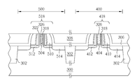
- a substrate 300 is provided, such as a silicon substrate, a silicon-containing substrate or a silicon-on-insulator (SOI) substrate.
- a plurality of shallow trench isolations (STI) 302 are disposed on the substrate 300 .
- the STI 302 can provide a stress.
- a first active region 400 and a second active region 500 which are insulated from each other, are defined on the substrate 300 .
- a first conductive type transistor 402 and a second conductive type transistor 502 are formed on the substrate 300 respectively in the first active region 400 and the second active region 500 .
- the first conductive type transistor 402 is a P-type transistor
- the second conductive type transistor 502 is an N-type transistor.
- the first conductive type transistor 402 includes a first gate dielectric layer 404 , a first sacrifice gate 406 , a first capping layer 408 , a first spacer 410 , a first light doped drain (LDD) 412 and a first source/drain 414 .
- the first gate dielectric layer 404 can be a SiO 2 layer or a high-K gate dielectric layer.
- the high-k gate dielectric layer includes silicon nitride (SiN), silicon oxynitride (SiON) and metal oxide.
- the metal oxide comprises rare earth metal oxide, such as hafnium oxide (HfO 2 ), hafnium silicon oxide (HfSiO 4 ), hafnium silicon oxynitride (HfSiON), aluminum oxide (Al 2 O 3 ), lanthanum oxide (La 2 O 3 ), lanthanum aluminum oxide (LaAlO), tantalum oxide (Ta 2 O 5 ), zirconium oxide (ZrO 2 ), zirconium silicon oxide (ZrSiO 4 ), hafnium zirconium oxide (HfZrO), strontium bismuth tantalate (SrBi 2 Ta 2 O 9 , SBT), lead zirconate titanate (PbZr x Ti 1-x O 3 , PZT) or barium strontium titanate (Ba x Sr 1-x TiO 3 , BST), but is not limited thereto.
- rare earth metal oxide such as hafnium oxide (HfO 2 ), hafnium silicon oxide (H
- the first gate dielectric layer 404 may be single layer or a multi layer and preferably includes a SiO 2 layer and a high-k dielectric layer from bottom to top in series.
- the first sacrifice gate 406 is a poly-silicon gate.
- the first sacrifice gate 406 is a multi-layered gate including a poly-silicon layer, an amorphous silicon layer or a germanium layer.
- the sacrifice gate 406 may include an inclined sidewall, thereby forming an “up-large-bottom-small” structure.
- a barrier layer or an etch stop layer can be optionally formed between the first gate dielectric layer 404 and the first sacrifice gate 406 , for instance, a SiN layer or a metal nitride layer such as TiN or TaN.
- the first capping layer 408 is an optional layer including SiN layer, SiO 2 or their combination for example.
- the first spacer 410 can be a multilayered structure including high temperature oxide (HTO), SiN, SiO or SiN formed by hexachlorodisilane (Si 2 Cl 6 ) (HCD-SiN).
- HTO high temperature oxide
- SiN SiO
- SiN formed by hexachlorodisilane
- HCD-SiN hexachlorodisilane
- the first spacer 410 can be partially or completely removed to produce a desired stress of the contact etch stop layer (CESL) 306 toward the first conductive type transistor 402 and the second conductive type transistor 502 .
- the first LDD 412 and the first source/drain 414 are formed by appropriate implant doping.
- the second conductive type transistor 502 includes a second gate dielectric layer 504 , a second sacrifice gate 506 , a second capping layer 508 , a second spacer 510 , a second LDD 512 and a second source/drain 514 .
- the embodiment of each component in the second conductive type transistor 502 is similar to that of the first conductive type transistor 402 and is not described repeatedly.
- the first conductive type transistor 402 and the second conductive type transistor 502 can further include other semiconductor structures which are not explicitly shown in FIG.
- a contact etch stop layer (CESL) 306 and an inter-layer dielectric (ILD) layer 308 are formed on the substrate 300 to cover the first conductive type transistor 402 and the second conductive type transistor 502 .
- the CESL 306 can generate a stress to form a selective strain scheme (SSS) wherein a compressing force is applied on the first conductive type electrode 402 and a straining force is applied on the second conductive type electrode 502 .
- SSS selective strain scheme
- a planarization process such as a chemical mechanical polish (CMP) process or an etching-back process or their combination is performed to remove a part of the ILD layer 308 , a part of the CESL 306 , a part of the first spacer 410 , a part of the second spacer 510 , and completely remove the first capping layer 408 and the second capping layer 508 , until the top surface of the first sacrifice gate 406 and the second sacrifice gate 506 are exposed.
- CMP chemical mechanical polish
- a mask layer 312 and an optional auxiliary layer 314 are formed on the substrate 300 .
- the mask layer 312 is a TiN layer
- the auxiliary layer 314 is a SiO 2 layer.
- the auxiliary layer 314 can provide a better adhesion force toward the first patterned photoresist layer 316 which is formed in the follow-up step.
- the thickness of the mask layer 312 is about 50 ⁇ 150 A (angstrom), preferably 100 A
- the thickness of the auxiliary layer 314 is about 0 ⁇ 50 A, preferably 20 A. However, the thickness is not limited thereto.
- a first patterned photoresist layer 316 is formed on the substrate 300 to cover at least the second active region 500 .
- the first patterned photoresist layer 316 as a mask, a portion of the mask layer 312 , the auxiliary layer 314 and the first sacrifice gate 406 not covered by the first patterned photoresist layer 316 are removed away.
- the above steps are accomplished by patterning the mask layer 312 and then using the patterned mask layer 312 as a mask to remove the first sacrifice gate 406 .
- the material used for the first sacrifice gate 406 typically includes poly-silicon, although the wet etching process having a better etching selectivity can stop on the first gate dielectric layer 404 , the under-cut phenomenon easily occurs when using the mask layer 312 as a mask to remove the below poly-silicon.
- one embodiment of the present invention is to perform a dry etching process first to remove the large part of the first sacrifice gate 406 and then to perform a wet etching process to thoroughly remove the first sacrifice gate 406 and stop on the first gate dielectric layer 404 .
- FIG. 4 a to FIG. 7 b please refer to FIG. 4 a to FIG. 7 b , wherein FIG. 4 b and FIG.
- FIG. 7 b show a semiconductor structure having a poly-silicon gate interface between PMOS and NMOS.
- FIG. 4 b and FIG. 7 b represent the cross-sectional view of FIG. 4 a and FIG. 7 a , respectively, and the cross line corresponds to the second sacrifice gate 506 .
- the dashed line I in FIG. 4 b and FIG. 7 b represents the position of the poly-silicon gate interface.
- the right part of the dashed line I represents a P-type transistor while the left part of the dashed line I represents an N-type transistor.
- a dry etching step is performed to remove the mask layer 316 , the auxiliary layer 312 and a part of the first sacrifice gate 406 not covered by the first patterned photoresist layer 316 .
- a trimmed process is performed toward the first patterned photoresist layer 316 .
- the sidewall of the first patterned photoresist layer 316 is trimmed, and the width of the first patterned photoresist layer 316 is slightly reduced.
- the first patterned photoresist layer 316 evenly shrinks inwardly to form a second patterned photoresist layer 317 .
- the sidewall of the first patterned photoresist layer 316 is originally near the first sacrifice gate 416 , and after the photoresist trimming process, the first patterned photoresist layer 316 shrinks back toward the second sacrifice gate 516 , thereby forming the second patterned photoresist layer 317 .
- the covering area of the second patterned photoresist layer 317 is smaller than that of the first patterned photoresist layer 316 .
- the mask layer 312 and the auxiliary layer 314 not covered by the second patterned photoresist layer 317 are removed.
- a wet etch is performed to completely remove the first sacrifice gate 406 .
- a first trench 416 is formed in the first conductive type transistor 402 .
- the second sacrifice gate 506 of the second conductive type transistor 502 is not removed away since it is covered by the mask layer 312 .
- the poly-silicon sidewall is formed accurately near the dashed line I.
- an annealing step can be performed.
- the annealing process is performed by treating with heat under about 500° C. to 700° C. in a rapid thermal annealing (RTA) equipment or a laser annealing system, or by treating with UV light under about 300° C. to 450° C.
- RTA rapid thermal annealing
- a dry etch step or a wet etch step or their combination can be performed to remove the upper part of the first spacer 410 by forming a photoresist covering the lower part of the first trench 416 .
- the first spacer 410 near region A can be removed, so as to enlarge the upper opening of the first trench 416 .
- a P type work function metal layer 318 is formed on the substrate 300 .
- the P type work function metal layer 318 is formed conformally on the surface of the first trench 416 where the first trench 416 is not completely filled with the P type work function metal layer 318 .
- the P type work function metal layer 318 serves as a work function metal required by a P-type transistor including Ni, Pd, Pt, Be, Ir, Te, Re, Ru, Rh, W, Mo, or WN, RuN, MoN, TiN, TaN, or WC, TaC, TiC, or TiAlN, TaAlN, but should not be limited thereto.
- the P type work function metal layer 318 can include the same material or different material as the mask layer 312 .
- the P type work function metal layer 318 includes the material having etching selectivity substantially close to that of the mask layer 312 .
- the P type work function metal layer 318 includes the same material as is used in the mask layer 312 .
- a third patterned photoresist layer 320 is formed on the substrate 300 to cover at least the first active region 400 .
- a part of the P type work function metal layer 318 and the mask layer 312 which are not covered by the third patterned photoresist layer 32 o are removed, thereby exposing the second sacrifice gate 506 .
- the third patterned photoresist layer 32 o is removed. It is understood that step of using the third patterned photoresist layer 32 o as a mask may include the trimming step described above.
- the second sacrifice gate 506 is removed by using a dry etching process and/or a wet etching process, thereby forming a second trench 516 in the second conductive type transistor 502 .
- an annealing process can be performed to restore the stress generated by the CESL 306 .
- a dry etch step or a wet etch step or their combination can be performed to remove the upper part of the second spacer 510 by forming a photoresist covering the lower part of the second trench 516 , so as to enlarge the upper opening of the second trench 516 .
- an N type work function metal layer 322 is formed on the substrate 300 .
- the N type work function metal layer 322 is formed conformally on the surface of the second trench 516 and on the surface of the P type work function metal layer 318 in the first trench 416 . However, the first trench 416 and the second trench 516 are not completely filled with the N type work function metal layer 322 .
- the second metal layer 324 serves as a work function metal required by an N-type transistor including titanium aluminides (TiAl), aluminum zirconium (ZrAl), aluminum tungsten (WAl), aluminum tantalum (TaAl) or aluminum hafnium (HfAl), but should not be limited thereto.
- a barrier layer 324 can be formed optionally between the N type work function metal layer 322 and the metal layer 326 .
- the barrier layer 324 includes metal such as TiN.
- a low resistive metal layer 326 is formed on the substrate 300 . The metal layer 326 is formed on the N type work function metal layer 322 (if the barrier layer 324 is utilized, the metal layer 326 is formed on the barrier layer 324 ) and completely fills the first trench 416 and the second trench 516 .
- a planarization process is performed to simultaneously remove the P type work function metal layer 318 , the N type work function metal layer 322 , (the barrier layer 324 ) and the metal layer 326 outside the first trench 416 and the second trench 516 .
- the P type work function metal layer 318 , the N type work function metal layer 322 , (the barrier layer 324 ) and the metal layer 326 in the first trench 416 together form a first metal gate 418 of the first conductive type transistor 402 (P-type transistor), which has a work function substantially between 4.8 eV and 5.2 eV.
- a contact plug forming process can be carried out, for example, a contact plug having a stress can be formed.
- the ILD layer 306 and the CESL 308 can be removed completely.
- at least one CESL can be formed on the substrate 300 .
- the new CESL can generate a stress, thereby enhancing the efficiency of the first conductive type transistor 402 and the second conductive type transistor 502 , respectively.
- Another ILD layer (not shown) is then formed and at least a contact plug having appropriate stress can be formed therein.
- the above methods present forming the high-k gate dielectric layer at first (namely, the high-K first process).
- a high-K gate dielectric layer can be formed on the surface of the first trench 416 before forming the P type work function metal layer 318 .
- the P type work function metal layer 318 and the metal layer 326 are formed on the high-K gate dielectric layer in the first trench 416 .
- the high-K gate dielectric layer and the P type work function metal layer 318 will form a U shape in their cross section.
- the material of the dielectric layer formed under the sacrifice gate is not limited to high-k material but can include another dielectric material such as SiO 2 . Please refer to FIG. 13 to FIG.
- FIG. 13 illustrating schematic diagrams of the method of manufacturing the semiconductor device having metal gates according to the second embodiment of the present invention.
- the former steps of the second embodiment are similar to those in FIG. 1 to FIG. 2 of the first embodiment and repeated descriptions are omitted.
- a mask layer 312 , an auxiliary layer 314 and a first patterned photoresist layer 319 are formed on the substrate 300 .
- the first patterned photoresist layer 319 at least covers the first active region 400 .
- step of using the first patterned photoresist layer 319 as a mask may include the trimming step described in the first embodiment. Or, a dry etch step or a wet etch step or their combination can be performed to enlarge the upper opening of the second trench 516 .
- an N type work function metal layer 322 is formed on the substrate 300 .
- the N type work function metal layer 322 is formed on the surface of the second trench 516 , where the second trench 516 is not completely filled with the N type work function metal layer 322 .
- a third patterned photoresist layer 321 is formed on the substrate 300 to cover at least the second active region 500 .
- FIG. 17 by using the third patterned photoresist layer 321 as a mask, a part of the N type work function metal layer 322 and the mask layer 312 which are not covered by the third patterned photoresist layer 321 are removed, thereby exposing the first sacrifice gate 406 .
- the third patterned photoresist layer 321 is removed. It is understood that step of using the third patterned photoresist layer 321 as a mask may include the trimming step described in the first embodiment.
- the first sacrifice gate 406 is removed by using a dry etching process and/or a wet etching process, thereby forming a first trench 416 in the first conductive type transistor 402 .
- An annealing process can be carried out to restore the stress generated by the CESL 306 .
- a dry etch step or a wet etch step or their combination can be performed to enlarge the upper opening of the first trench 416 .
- a P type work function metal layer 318 is formed on the substrate 300 .
- the P type work function metal layer 318 is formed on the surface of the first trench 416 and on the surface of the N type work function metal layer 322 in the second trench 516 .
- first trench 416 and the second trench 516 are not completely filled with the P type work function metal layer 322 .
- a low resistive metal layer 326 can be formed directly on the P type work function metal layer 322 and completely fills the first trench 416 and the second trench 516 .
- first metal gate 418 of the first conductive type transistor 402 (P-type transistor), which has a work function substantially between 4.8 eV and 5.2 eV.
- the N type work function metal layer 322 , the P type work function metal layer 318 and the metal layer 326 in the second trench 516 together form a second metal gate 518 of the second conductive type transistor 502 (N-type transistor) which has a work function substantially between 3.9 eV and 4.3 eV.
- the P type work function metal layer 318 can also serve a good material for barrier (TiN), comparing with the first embodiment, there is no need to further form a barrier layer between the N type work function metal layer 322 and the metal layer 326 in the present embodiment.
- the P type work function metal layer 318 can serve both the functions of the P type work function metal layer and the barrier layer. As a result, the stack number of the metal layers in the first type conductive type transistor 402 and the second type conductive transistor 502 can be reduced and the problem of poor metal gap filling capability can be overcome.
- a contact plug or a CESL having appropriate stress can be formed according to the selective stress system. Besides the high-k first process described above, it is also available to provide a high-k last process in the present embodiment.
- a passivating process can be carried out immediately after forming the N type work function metal layer 322 to produce a passivation structure on the surface of the N type work function metal layer 322 .
- the passivating process can be performed by utilizing ammonia (NH 4 OH), or a nitridation process or an oxidation process to passivate the surface of the N type work function metal layer 322 .
- the P type work function metal layer 318 or the metal layer 326 can be formed on the N type work function metal layer 322 as described in the above embodiments.
- the present invention provides a method of manufacturing semiconductor device having metal gates.
- the method includes forming the P type work function metal layer or the N type work function metal layer respectively in the first trench or the second trench, which is then filled with the metal layer.
- the present invention can prevent the bad metal layer (usually Al) filling issue.
- only one CMP process is needed in the present invention, so the yield of the method can be improved.
- the present invention also provides several embodiments, including forming a barrier layer, performing a passivating process, or directly using the P type work function metal layer as the barrier layer to ameliorate the method.
- the present invention also provides using a trimmed process and an annealing process when forming the first trench and the second trench, all of which can increase the reliability of the product.
Abstract
Description
Claims (20)
Priority Applications (1)
| Application Number | Priority Date | Filing Date | Title |
|---|---|---|---|
| US13/053,223 US8802524B2 (en) | 2011-03-22 | 2011-03-22 | Method of manufacturing semiconductor device having metal gates |
Applications Claiming Priority (1)
| Application Number | Priority Date | Filing Date | Title |
|---|---|---|---|
| US13/053,223 US8802524B2 (en) | 2011-03-22 | 2011-03-22 | Method of manufacturing semiconductor device having metal gates |
Publications (2)
| Publication Number | Publication Date |
|---|---|
| US20120244669A1 US20120244669A1 (en) | 2012-09-27 |
| US8802524B2 true US8802524B2 (en) | 2014-08-12 |
Family
ID=46877680
Family Applications (1)
| Application Number | Title | Priority Date | Filing Date |
|---|---|---|---|
| US13/053,223 Active 2031-11-22 US8802524B2 (en) | 2011-03-22 | 2011-03-22 | Method of manufacturing semiconductor device having metal gates |
Country Status (1)
| Country | Link |
|---|---|
| US (1) | US8802524B2 (en) |
Cited By (3)
| Publication number | Priority date | Publication date | Assignee | Title |
|---|---|---|---|---|
| US20130092992A1 (en) * | 2011-10-17 | 2013-04-18 | International Business Machines Corporation | Replacement gate multigate transistor for embedded dram |
| US20140349452A1 (en) * | 2013-05-22 | 2014-11-27 | United Microelectronics Corp. | Method for manufacturing semiconductor devices |
| US20150087144A1 (en) * | 2013-09-26 | 2015-03-26 | Taiwan Semiconductor Manufacturing Company Ltd. | Apparatus and method of manufacturing metal gate semiconductor device |
Families Citing this family (14)
| Publication number | Priority date | Publication date | Assignee | Title |
|---|---|---|---|---|
| US8481415B2 (en) * | 2010-12-02 | 2013-07-09 | International Business Machines Corporation | Self-aligned contact combined with a replacement metal gate/high-K gate dielectric |
| US8564063B2 (en) | 2010-12-07 | 2013-10-22 | United Microelectronics Corp. | Semiconductor device having metal gate and manufacturing method thereof |
| US9384962B2 (en) | 2011-04-07 | 2016-07-05 | United Microelectronics Corp. | Oxygen treatment of replacement work-function metals in CMOS transistor gates |
| US8765588B2 (en) | 2011-09-28 | 2014-07-01 | United Microelectronics Corp. | Semiconductor process |
| US8710593B2 (en) * | 2012-04-12 | 2014-04-29 | United Microelectronics Corp. | Resistor and manufacturing method thereof |
| US9130059B2 (en) * | 2013-01-18 | 2015-09-08 | Taiwan Semiconductor Manufacturing Company, Ltd. | Method of fabricating a semiconductor device having a capping layer |
| KR102066848B1 (en) | 2013-06-24 | 2020-01-16 | 삼성전자 주식회사 | Semiconductor device and method for fabricating the same |
| US20160013288A1 (en) * | 2014-07-09 | 2016-01-14 | United Microelectronics Corp. | Method of forming a metal gate structure |
| CN105826265B (en) * | 2015-01-09 | 2019-05-28 | 中芯国际集成电路制造(上海)有限公司 | The forming method of semiconductor devices |
| US20160322473A1 (en) * | 2015-04-30 | 2016-11-03 | Taiwan Semiconductor Manufacturing Company, Ltd. | Buffer Layer on Gate and Methods of Forming the Same |
| US9947594B2 (en) * | 2016-09-19 | 2018-04-17 | Taiwan Semiconductor Manufacturing Co., Ltd. | Semiconductor device and manufacturing method thereof |
| TWI712084B (en) * | 2016-11-17 | 2020-12-01 | 聯華電子股份有限公司 | Semiconductor device and manufacturing method thereof |
| US11183580B2 (en) * | 2019-05-30 | 2021-11-23 | Taiwan Semiconductor Manufacturing Co., Ltd. | Structure and formation method of semiconductor device with metal gate stack |
| US11342231B2 (en) | 2019-09-17 | 2022-05-24 | Taiwan Semiconductor Manufacturing Co., Ltd. | Integrated circuit device with low threshold voltage |
Citations (77)
| Publication number | Priority date | Publication date | Assignee | Title |
|---|---|---|---|---|
| US6033963A (en) | 1999-08-30 | 2000-03-07 | Taiwan Semiconductor Manufacturing Company | Method of forming a metal gate for CMOS devices using a replacement gate process |
| US6162694A (en) | 1998-11-25 | 2000-12-19 | Advanced Micro Devices, Inc. | Method of forming a metal gate electrode using replaced polysilicon structure |
| US6171910B1 (en) | 1999-07-21 | 2001-01-09 | Motorola Inc. | Method for forming a semiconductor device |
| US6406956B1 (en) | 2001-04-30 | 2002-06-18 | Taiwan Semiconductor Manufacturing Company | Poly resistor structure for damascene metal gate |
| US6524901B1 (en) | 2002-06-20 | 2003-02-25 | Micron Technology, Inc. | Method for forming a notched damascene planar poly/metal gate |
| US6617209B1 (en) | 2002-02-22 | 2003-09-09 | Intel Corporation | Method for making a semiconductor device having a high-k gate dielectric |
| US6617210B1 (en) | 2002-05-31 | 2003-09-09 | Intel Corporation | Method for making a semiconductor device having a high-k gate dielectric |
| US6653698B2 (en) | 2001-12-20 | 2003-11-25 | International Business Machines Corporation | Integration of dual workfunction metal gate CMOS devices |
| US6656764B1 (en) | 2002-05-15 | 2003-12-02 | Taiwan Semiconductor Manufacturing Company | Process for integration of a high dielectric constant gate insulator layer in a CMOS device |
| US6689675B1 (en) | 2002-10-31 | 2004-02-10 | Intel Corporation | Method for making a semiconductor device having a high-k gate dielectric |
| US6696327B1 (en) | 2003-03-18 | 2004-02-24 | Intel Corporation | Method for making a semiconductor device having a high-k gate dielectric |
| US6696333B1 (en) | 1999-11-30 | 2004-02-24 | Intel Corporation | Method of making integrated circuit with MOSFETs having bi-layer metal gate electrodes |
| US6709911B1 (en) | 2003-01-07 | 2004-03-23 | Intel Corporation | Method for making a semiconductor device having a high-k gate dielectric |
| US6713358B1 (en) | 2002-11-05 | 2004-03-30 | Intel Corporation | Method for making a semiconductor device having a high-k gate dielectric |
| US6716707B1 (en) | 2003-03-11 | 2004-04-06 | Intel Corporation | Method for making a semiconductor device having a high-k gate dielectric |
| US6770568B2 (en) | 2002-09-12 | 2004-08-03 | Intel Corporation | Selective etching using sonication |
| US6787440B2 (en) | 2002-12-10 | 2004-09-07 | Intel Corporation | Method for making a semiconductor device having an ultra-thin high-k gate dielectric |
| US6797622B2 (en) | 2002-07-31 | 2004-09-28 | Intel Corporation | Selective etching of polysilicon |
| US6806146B1 (en) | 2003-05-20 | 2004-10-19 | Intel Corporation | Method for making a semiconductor device having a high-k gate dielectric |
| US6830953B1 (en) | 2002-09-17 | 2004-12-14 | Taiwan Semiconductor Manufacturing Company, Ltd. | Suppression of MOSFET gate leakage current |
| US6858483B2 (en) | 2002-12-20 | 2005-02-22 | Intel Corporation | Integrating n-type and p-type metal gate transistors |
| US20050048722A1 (en) * | 2003-08-26 | 2005-03-03 | Tomohiro Saito | Method of manufacturing semiconductor device |
| US6887800B1 (en) | 2004-06-04 | 2005-05-03 | Intel Corporation | Method for making a semiconductor device with a high-k gate dielectric and metal layers that meet at a P/N junction |
| US6900481B2 (en) | 2002-02-21 | 2005-05-31 | Intel Corporation | Non-silicon semiconductor and high-k gate dielectric metal oxide semiconductor field effect transistors |
| US6921711B2 (en) * | 2003-09-09 | 2005-07-26 | International Business Machines Corporation | Method for forming metal replacement gate of high performance |
| US6939815B2 (en) | 2003-08-28 | 2005-09-06 | Intel Corporation | Method for making a semiconductor device having a high-k gate dielectric |
| US6967131B2 (en) | 2003-10-29 | 2005-11-22 | International Business Machines Corp. | Field effect transistor with electroplated metal gate |
| US20060008954A1 (en) | 2003-12-29 | 2006-01-12 | Jack Kavalieros | Methods for integrating replacement metal gate structures |
| US7029966B2 (en) | 2003-09-18 | 2006-04-18 | International Business Machines Corporation | Process options of forming silicided metal gates for advanced CMOS devices |
| US7045428B2 (en) | 2004-05-26 | 2006-05-16 | Intel Corporation | Method for making a semiconductor device with a high-k gate dielectric and a conductor that facilitates current flow across a P/N junction |
| US7056794B2 (en) | 2004-01-09 | 2006-06-06 | International Business Machines Corporation | FET gate structure with metal gate electrode and silicide contact |
| US7064050B2 (en) | 2003-11-28 | 2006-06-20 | International Business Machines Corporation | Metal carbide gate structure and method of fabrication |
| US7064066B1 (en) | 2004-12-07 | 2006-06-20 | Intel Corporation | Method for making a semiconductor device having a high-k gate dielectric and a titanium carbide gate electrode |
| US7126199B2 (en) | 2004-09-27 | 2006-10-24 | Intel Corporation | Multilayer metal gate electrode |
| US7138323B2 (en) | 2004-07-28 | 2006-11-21 | Intel Corporation | Planarizing a semiconductor structure to form replacement metal gates |
| US7144783B2 (en) | 2004-04-30 | 2006-12-05 | Intel Corporation | Reducing gate dielectric material to form a metal gate electrode extension |
| US7148099B2 (en) | 2004-06-24 | 2006-12-12 | Intel Corporation | Reducing the dielectric constant of a portion of a gate dielectric |
| US7148548B2 (en) | 2004-07-20 | 2006-12-12 | Intel Corporation | Semiconductor device with a high-k gate dielectric and a metal gate electrode |
| US7153734B2 (en) | 2003-12-29 | 2006-12-26 | Intel Corporation | CMOS device with metal and silicide gate electrodes and a method for making it |
| US7153784B2 (en) | 2004-04-20 | 2006-12-26 | Intel Corporation | Method for making a semiconductor device having a high-k gate dielectric layer and a metal gate electrode |
| US7157378B2 (en) | 2004-07-06 | 2007-01-02 | Intel Corporation | Method for making a semiconductor device having a high-k gate dielectric layer and a metal gate electrode |
| US7160767B2 (en) | 2003-12-18 | 2007-01-09 | Intel Corporation | Method for making a semiconductor device that includes a metal gate electrode |
| US7163853B2 (en) | 2005-02-09 | 2007-01-16 | Taiwan Semiconductor Manufacturing Company, Ltd. | Method of manufacturing a capacitor and a metal gate on a semiconductor device |
| US7176090B2 (en) | 2004-09-07 | 2007-02-13 | Intel Corporation | Method for making a semiconductor device that includes a metal gate electrode |
| US7176537B2 (en) | 2005-05-23 | 2007-02-13 | Taiwan Semiconductor Manufacturing Company, Ltd. | High performance CMOS with metal-gate and Schottky source/drain |
| US7183184B2 (en) | 2003-12-29 | 2007-02-27 | Intel Corporation | Method for making a semiconductor device that includes a metal gate electrode |
| US7192890B2 (en) | 2003-10-29 | 2007-03-20 | Intel Corporation | Depositing an oxide |
| US7196856B2 (en) | 2003-06-13 | 2007-03-27 | Enplas Corporation | Imaging lens system |
| US7208361B2 (en) | 2004-03-24 | 2007-04-24 | Intel Corporation | Replacement gate process for making a semiconductor device that includes a metal gate electrode |
| US7220365B2 (en) | 2001-08-13 | 2007-05-22 | New Qu Energy Ltd. | Devices using a medium having a high heat transfer rate |
| US20070141798A1 (en) | 2005-12-20 | 2007-06-21 | Intel Corporation | Silicide layers in contacts for high-k/metal gate transistors |
| US7271045B2 (en) | 2005-09-30 | 2007-09-18 | Intel Corporation | Etch stop and hard mask film property matching to enable improved replacement metal gate process |
| US7271083B2 (en) | 2004-07-22 | 2007-09-18 | Taiwan Semiconductor Manufacturing Company, Ltd. | One-transistor random access memory technology compatible with metal gate process |
| US7285829B2 (en) | 2004-03-31 | 2007-10-23 | Intel Corporation | Semiconductor device having a laterally modulated gate workfunction and method of fabrication |
| US20070262451A1 (en) | 2006-05-09 | 2007-11-15 | Willy Rachmady | Recessed workfunction metal in CMOS transistor gates |
| US7332439B2 (en) | 2004-09-29 | 2008-02-19 | Intel Corporation | Metal gate transistors with epitaxial source and drain regions |
| US7365015B2 (en) | 2004-07-13 | 2008-04-29 | Lsi Logic Corporation | Damascene replacement metal gate process with controlled gate profile and length using Si1-xGex as sacrificial material |
| US7381608B2 (en) | 2004-12-07 | 2008-06-03 | Intel Corporation | Method for making a semiconductor device with a high-k gate dielectric and a metal gate electrode |
| US7384880B2 (en) | 2004-10-12 | 2008-06-10 | Intel Corporation | Method for making a semiconductor device having a high-k gate dielectric |
| US7387927B2 (en) | 2004-09-10 | 2008-06-17 | Intel Corporation | Reducing oxidation under a high K gate dielectric |
| US7390709B2 (en) | 2004-09-08 | 2008-06-24 | Intel Corporation | Method for making a semiconductor device having a high-k gate dielectric layer and a metal gate electrode |
| US7422936B2 (en) | 2004-08-25 | 2008-09-09 | Intel Corporation | Facilitating removal of sacrificial layers via implantation to form replacement metal gates |
| US7425490B2 (en) | 2004-06-24 | 2008-09-16 | Intel Corporation | Reducing reactions between polysilicon gate electrodes and high dielectric constant gate dielectrics |
| US7439113B2 (en) | 2004-07-12 | 2008-10-21 | Intel Corporation | Forming dual metal complementary metal oxide semiconductor integrated circuits |
| US20090039433A1 (en) | 2007-08-08 | 2009-02-12 | Taiwan Semiconductor Manufacturing Company, Ltd. | Semiconductor device with high-k/dual metal gate |
| US20090087974A1 (en) | 2007-09-29 | 2009-04-02 | Andrew Waite | Method of forming high-k gate electrode structures after transistor fabrication |
| US7531404B2 (en) | 2005-08-30 | 2009-05-12 | Intel Corporation | Semiconductor device having a metal gate electrode formed on an annealed high-k gate dielectric layer |
| US7569443B2 (en) | 2005-06-21 | 2009-08-04 | Intel Corporation | Complementary metal oxide semiconductor integrated circuit using raised source drain and replacement metal gate |
| US7595248B2 (en) | 2005-12-01 | 2009-09-29 | Intel Corporation | Angled implantation for removal of thin film layers |
| US20100044783A1 (en) | 2008-08-20 | 2010-02-25 | Taiwan Semiconductor Manufacturing Company, Ltd. | Integrated circuit metal gate structure and method of fabrication |
| US20100052066A1 (en) | 2008-08-26 | 2010-03-04 | Taiwan Semiconductor Manufacturing Company, Ltd. | structure and method for a cmos device with doped conducting metal oxide as the gate electrode |
| US20100065926A1 (en) | 2008-09-12 | 2010-03-18 | Taiwan Semiconductor Manufacturing Company, Ltd. | Photoresist etch back method for gate last process |
| US20100068877A1 (en) * | 2008-09-12 | 2010-03-18 | Taiwan Semiconductor Manufacturing Company, Ltd. | Method for tuning a work function of high-k metal gate devices |
| US20100127336A1 (en) * | 2008-11-21 | 2010-05-27 | Texas Instruments Incorporated | Structure and method for metal gate stack oxygen concentration control using an oxygen diffusion barrier layer and a sacrificial oxygen gettering layer |
| US20110018072A1 (en) * | 2008-08-26 | 2011-01-27 | Chien-Ting Lin | Metal gate transistor and method for fabricating the same |
| US20120256276A1 (en) * | 2011-04-07 | 2012-10-11 | Guang-Yaw Hwang | Metal Gate and Fabricating Method Thereof |
| US8574990B2 (en) * | 2011-02-24 | 2013-11-05 | United Microelectronics Corp. | Method of manufacturing semiconductor device having metal gate |
-
2011
- 2011-03-22 US US13/053,223 patent/US8802524B2/en active Active
Patent Citations (95)
| Publication number | Priority date | Publication date | Assignee | Title |
|---|---|---|---|---|
| US6162694A (en) | 1998-11-25 | 2000-12-19 | Advanced Micro Devices, Inc. | Method of forming a metal gate electrode using replaced polysilicon structure |
| US6171910B1 (en) | 1999-07-21 | 2001-01-09 | Motorola Inc. | Method for forming a semiconductor device |
| US6033963A (en) | 1999-08-30 | 2000-03-07 | Taiwan Semiconductor Manufacturing Company | Method of forming a metal gate for CMOS devices using a replacement gate process |
| US6879009B2 (en) | 1999-11-30 | 2005-04-12 | Intel Corporation | Integrated circuit with MOSFETS having bi-layer metal gate electrodes |
| US6696333B1 (en) | 1999-11-30 | 2004-02-24 | Intel Corporation | Method of making integrated circuit with MOSFETs having bi-layer metal gate electrodes |
| US6406956B1 (en) | 2001-04-30 | 2002-06-18 | Taiwan Semiconductor Manufacturing Company | Poly resistor structure for damascene metal gate |
| US7220365B2 (en) | 2001-08-13 | 2007-05-22 | New Qu Energy Ltd. | Devices using a medium having a high heat transfer rate |
| US6653698B2 (en) | 2001-12-20 | 2003-11-25 | International Business Machines Corporation | Integration of dual workfunction metal gate CMOS devices |
| US6900481B2 (en) | 2002-02-21 | 2005-05-31 | Intel Corporation | Non-silicon semiconductor and high-k gate dielectric metal oxide semiconductor field effect transistors |
| US6617209B1 (en) | 2002-02-22 | 2003-09-09 | Intel Corporation | Method for making a semiconductor device having a high-k gate dielectric |
| US7166505B2 (en) | 2002-02-22 | 2007-01-23 | Intel Corporation | Method for making a semiconductor device having a high-k gate dielectric |
| US6656764B1 (en) | 2002-05-15 | 2003-12-02 | Taiwan Semiconductor Manufacturing Company | Process for integration of a high dielectric constant gate insulator layer in a CMOS device |
| US6914313B2 (en) | 2002-05-15 | 2005-07-05 | Taiwan Semiconductor Manufacturing Company, Ltd. | Process for integration of a high dielectric constant gate insulator layer in a CMOS device |
| US7393766B2 (en) | 2002-05-15 | 2008-07-01 | Taiwan Semiconductor Manufacturing Company, Ltd. | Process for integration of a high dielectric constant gate insulator layer in a CMOS device |
| US6617210B1 (en) | 2002-05-31 | 2003-09-09 | Intel Corporation | Method for making a semiconductor device having a high-k gate dielectric |
| US6524901B1 (en) | 2002-06-20 | 2003-02-25 | Micron Technology, Inc. | Method for forming a notched damascene planar poly/metal gate |
| US6797622B2 (en) | 2002-07-31 | 2004-09-28 | Intel Corporation | Selective etching of polysilicon |
| US6770568B2 (en) | 2002-09-12 | 2004-08-03 | Intel Corporation | Selective etching using sonication |
| US6949769B2 (en) | 2002-09-17 | 2005-09-27 | Taiwan Semiconductor Manufacturing Company, Ltd. | Suppression of MOSFET gate leakage current |
| US6830953B1 (en) | 2002-09-17 | 2004-12-14 | Taiwan Semiconductor Manufacturing Company, Ltd. | Suppression of MOSFET gate leakage current |
| US6689675B1 (en) | 2002-10-31 | 2004-02-10 | Intel Corporation | Method for making a semiconductor device having a high-k gate dielectric |
| US6713358B1 (en) | 2002-11-05 | 2004-03-30 | Intel Corporation | Method for making a semiconductor device having a high-k gate dielectric |
| US6787440B2 (en) | 2002-12-10 | 2004-09-07 | Intel Corporation | Method for making a semiconductor device having an ultra-thin high-k gate dielectric |
| US7316949B2 (en) | 2002-12-20 | 2008-01-08 | Intel Corporation | Integrating n-type and p-type metal gate transistors |
| US6858483B2 (en) | 2002-12-20 | 2005-02-22 | Intel Corporation | Integrating n-type and p-type metal gate transistors |
| US6972225B2 (en) | 2002-12-20 | 2005-12-06 | Intel Corporation | integrating n-type and P-type metal gate transistors |
| US6953719B2 (en) | 2002-12-20 | 2005-10-11 | Intel Corporation | Integrating n-type and p-type metal gate transistors |
| US6709911B1 (en) | 2003-01-07 | 2004-03-23 | Intel Corporation | Method for making a semiconductor device having a high-k gate dielectric |
| US6716707B1 (en) | 2003-03-11 | 2004-04-06 | Intel Corporation | Method for making a semiconductor device having a high-k gate dielectric |
| US6897134B2 (en) | 2003-03-18 | 2005-05-24 | Intel Corporation | Method for making a semiconductor device having a high-k gate dielectric |
| US6696327B1 (en) | 2003-03-18 | 2004-02-24 | Intel Corporation | Method for making a semiconductor device having a high-k gate dielectric |
| US6806146B1 (en) | 2003-05-20 | 2004-10-19 | Intel Corporation | Method for making a semiconductor device having a high-k gate dielectric |
| US6867102B2 (en) | 2003-05-20 | 2005-03-15 | Intel Corporation | Method for making a semiconductor device having a high-k gate dielectric |
| US7196856B2 (en) | 2003-06-13 | 2007-03-27 | Enplas Corporation | Imaging lens system |
| US20050048722A1 (en) * | 2003-08-26 | 2005-03-03 | Tomohiro Saito | Method of manufacturing semiconductor device |
| US6939815B2 (en) | 2003-08-28 | 2005-09-06 | Intel Corporation | Method for making a semiconductor device having a high-k gate dielectric |
| US6921711B2 (en) * | 2003-09-09 | 2005-07-26 | International Business Machines Corporation | Method for forming metal replacement gate of high performance |
| US7326610B2 (en) | 2003-09-18 | 2008-02-05 | International Business Machines Corporation | Process options of forming silicided metal gates for advanced CMOS devices |
| US7029966B2 (en) | 2003-09-18 | 2006-04-18 | International Business Machines Corporation | Process options of forming silicided metal gates for advanced CMOS devices |
| US7112851B2 (en) | 2003-10-29 | 2006-09-26 | International Business Machines Corporation | Field effect transistor with electroplated metal gate |
| US7192890B2 (en) | 2003-10-29 | 2007-03-20 | Intel Corporation | Depositing an oxide |
| US6967131B2 (en) | 2003-10-29 | 2005-11-22 | International Business Machines Corp. | Field effect transistor with electroplated metal gate |
| US7064050B2 (en) | 2003-11-28 | 2006-06-20 | International Business Machines Corporation | Metal carbide gate structure and method of fabrication |
| US7160767B2 (en) | 2003-12-18 | 2007-01-09 | Intel Corporation | Method for making a semiconductor device that includes a metal gate electrode |
| US20060008954A1 (en) | 2003-12-29 | 2006-01-12 | Jack Kavalieros | Methods for integrating replacement metal gate structures |
| US7217611B2 (en) | 2003-12-29 | 2007-05-15 | Intel Corporation | Methods for integrating replacement metal gate structures |
| US7183184B2 (en) | 2003-12-29 | 2007-02-27 | Intel Corporation | Method for making a semiconductor device that includes a metal gate electrode |
| US7153734B2 (en) | 2003-12-29 | 2006-12-26 | Intel Corporation | CMOS device with metal and silicide gate electrodes and a method for making it |
| US7056794B2 (en) | 2004-01-09 | 2006-06-06 | International Business Machines Corporation | FET gate structure with metal gate electrode and silicide contact |
| US7208361B2 (en) | 2004-03-24 | 2007-04-24 | Intel Corporation | Replacement gate process for making a semiconductor device that includes a metal gate electrode |
| US7285829B2 (en) | 2004-03-31 | 2007-10-23 | Intel Corporation | Semiconductor device having a laterally modulated gate workfunction and method of fabrication |
| US7153784B2 (en) | 2004-04-20 | 2006-12-26 | Intel Corporation | Method for making a semiconductor device having a high-k gate dielectric layer and a metal gate electrode |
| US7355281B2 (en) | 2004-04-20 | 2008-04-08 | Intel Corporation | Method for making semiconductor device having a high-k gate dielectric layer and a metal gate electrode |
| US7144783B2 (en) | 2004-04-30 | 2006-12-05 | Intel Corporation | Reducing gate dielectric material to form a metal gate electrode extension |
| US20070040227A1 (en) | 2004-04-30 | 2007-02-22 | Suman Datta | Reducing gate dielectric material to form a metal gate electrode extension |
| US7045428B2 (en) | 2004-05-26 | 2006-05-16 | Intel Corporation | Method for making a semiconductor device with a high-k gate dielectric and a conductor that facilitates current flow across a P/N junction |
| US6887800B1 (en) | 2004-06-04 | 2005-05-03 | Intel Corporation | Method for making a semiconductor device with a high-k gate dielectric and metal layers that meet at a P/N junction |
| US20070029627A1 (en) | 2004-06-24 | 2007-02-08 | Suman Datta | Reducing the dielectric constant of a portion of a gate dielectric |
| US7148099B2 (en) | 2004-06-24 | 2006-12-12 | Intel Corporation | Reducing the dielectric constant of a portion of a gate dielectric |
| US7425490B2 (en) | 2004-06-24 | 2008-09-16 | Intel Corporation | Reducing reactions between polysilicon gate electrodes and high dielectric constant gate dielectrics |
| US7157378B2 (en) | 2004-07-06 | 2007-01-02 | Intel Corporation | Method for making a semiconductor device having a high-k gate dielectric layer and a metal gate electrode |
| US7439113B2 (en) | 2004-07-12 | 2008-10-21 | Intel Corporation | Forming dual metal complementary metal oxide semiconductor integrated circuits |
| US7365015B2 (en) | 2004-07-13 | 2008-04-29 | Lsi Logic Corporation | Damascene replacement metal gate process with controlled gate profile and length using Si1-xGex as sacrificial material |
| US7148548B2 (en) | 2004-07-20 | 2006-12-12 | Intel Corporation | Semiconductor device with a high-k gate dielectric and a metal gate electrode |
| US7271083B2 (en) | 2004-07-22 | 2007-09-18 | Taiwan Semiconductor Manufacturing Company, Ltd. | One-transistor random access memory technology compatible with metal gate process |
| US7138323B2 (en) | 2004-07-28 | 2006-11-21 | Intel Corporation | Planarizing a semiconductor structure to form replacement metal gates |
| US20070037372A1 (en) * | 2004-07-28 | 2007-02-15 | Jack Kavalieros | Planarizing a semiconductor structure to form replacement metal gates |
| US7422936B2 (en) | 2004-08-25 | 2008-09-09 | Intel Corporation | Facilitating removal of sacrificial layers via implantation to form replacement metal gates |
| US7176090B2 (en) | 2004-09-07 | 2007-02-13 | Intel Corporation | Method for making a semiconductor device that includes a metal gate electrode |
| US7390709B2 (en) | 2004-09-08 | 2008-06-24 | Intel Corporation | Method for making a semiconductor device having a high-k gate dielectric layer and a metal gate electrode |
| US7387927B2 (en) | 2004-09-10 | 2008-06-17 | Intel Corporation | Reducing oxidation under a high K gate dielectric |
| US7126199B2 (en) | 2004-09-27 | 2006-10-24 | Intel Corporation | Multilayer metal gate electrode |
| US7332439B2 (en) | 2004-09-29 | 2008-02-19 | Intel Corporation | Metal gate transistors with epitaxial source and drain regions |
| US7384880B2 (en) | 2004-10-12 | 2008-06-10 | Intel Corporation | Method for making a semiconductor device having a high-k gate dielectric |
| US7317231B2 (en) | 2004-12-07 | 2008-01-08 | Intel Corporation | Method for making a semiconductor device having a high-K gate dielectric and a titanium carbide gate electrode |
| US7381608B2 (en) | 2004-12-07 | 2008-06-03 | Intel Corporation | Method for making a semiconductor device with a high-k gate dielectric and a metal gate electrode |
| US7064066B1 (en) | 2004-12-07 | 2006-06-20 | Intel Corporation | Method for making a semiconductor device having a high-k gate dielectric and a titanium carbide gate electrode |
| US7163853B2 (en) | 2005-02-09 | 2007-01-16 | Taiwan Semiconductor Manufacturing Company, Ltd. | Method of manufacturing a capacitor and a metal gate on a semiconductor device |
| US7176537B2 (en) | 2005-05-23 | 2007-02-13 | Taiwan Semiconductor Manufacturing Company, Ltd. | High performance CMOS with metal-gate and Schottky source/drain |
| US7569443B2 (en) | 2005-06-21 | 2009-08-04 | Intel Corporation | Complementary metal oxide semiconductor integrated circuit using raised source drain and replacement metal gate |
| US7531404B2 (en) | 2005-08-30 | 2009-05-12 | Intel Corporation | Semiconductor device having a metal gate electrode formed on an annealed high-k gate dielectric layer |
| US7271045B2 (en) | 2005-09-30 | 2007-09-18 | Intel Corporation | Etch stop and hard mask film property matching to enable improved replacement metal gate process |
| US7595248B2 (en) | 2005-12-01 | 2009-09-29 | Intel Corporation | Angled implantation for removal of thin film layers |
| US20070141798A1 (en) | 2005-12-20 | 2007-06-21 | Intel Corporation | Silicide layers in contacts for high-k/metal gate transistors |
| US20070262451A1 (en) | 2006-05-09 | 2007-11-15 | Willy Rachmady | Recessed workfunction metal in CMOS transistor gates |
| US20090039433A1 (en) | 2007-08-08 | 2009-02-12 | Taiwan Semiconductor Manufacturing Company, Ltd. | Semiconductor device with high-k/dual metal gate |
| US20090087974A1 (en) | 2007-09-29 | 2009-04-02 | Andrew Waite | Method of forming high-k gate electrode structures after transistor fabrication |
| US20100044783A1 (en) | 2008-08-20 | 2010-02-25 | Taiwan Semiconductor Manufacturing Company, Ltd. | Integrated circuit metal gate structure and method of fabrication |
| US20100052066A1 (en) | 2008-08-26 | 2010-03-04 | Taiwan Semiconductor Manufacturing Company, Ltd. | structure and method for a cmos device with doped conducting metal oxide as the gate electrode |
| US20110018072A1 (en) * | 2008-08-26 | 2011-01-27 | Chien-Ting Lin | Metal gate transistor and method for fabricating the same |
| US20100065926A1 (en) | 2008-09-12 | 2010-03-18 | Taiwan Semiconductor Manufacturing Company, Ltd. | Photoresist etch back method for gate last process |
| US20100068877A1 (en) * | 2008-09-12 | 2010-03-18 | Taiwan Semiconductor Manufacturing Company, Ltd. | Method for tuning a work function of high-k metal gate devices |
| US20100127336A1 (en) * | 2008-11-21 | 2010-05-27 | Texas Instruments Incorporated | Structure and method for metal gate stack oxygen concentration control using an oxygen diffusion barrier layer and a sacrificial oxygen gettering layer |
| US8574990B2 (en) * | 2011-02-24 | 2013-11-05 | United Microelectronics Corp. | Method of manufacturing semiconductor device having metal gate |
| US20120256276A1 (en) * | 2011-04-07 | 2012-10-11 | Guang-Yaw Hwang | Metal Gate and Fabricating Method Thereof |
Cited By (5)
| Publication number | Priority date | Publication date | Assignee | Title |
|---|---|---|---|---|
| US20130092992A1 (en) * | 2011-10-17 | 2013-04-18 | International Business Machines Corporation | Replacement gate multigate transistor for embedded dram |
| US9368502B2 (en) * | 2011-10-17 | 2016-06-14 | GlogalFoundries, Inc. | Replacement gate multigate transistor for embedded DRAM |
| US20140349452A1 (en) * | 2013-05-22 | 2014-11-27 | United Microelectronics Corp. | Method for manufacturing semiconductor devices |
| US9196542B2 (en) * | 2013-05-22 | 2015-11-24 | United Microelectronics Corp. | Method for manufacturing semiconductor devices |
| US20150087144A1 (en) * | 2013-09-26 | 2015-03-26 | Taiwan Semiconductor Manufacturing Company Ltd. | Apparatus and method of manufacturing metal gate semiconductor device |
Also Published As
| Publication number | Publication date |
|---|---|
| US20120244669A1 (en) | 2012-09-27 |
Similar Documents
| Publication | Publication Date | Title |
|---|---|---|
| US8802524B2 (en) | Method of manufacturing semiconductor device having metal gates | |
| US9384962B2 (en) | Oxygen treatment of replacement work-function metals in CMOS transistor gates | |
| US9018086B2 (en) | Semiconductor device having a metal gate and fabricating method thereof | |
| US9754841B2 (en) | Method of forming integrated circuit having plural transistors with work function metal gate structures | |
| US8574990B2 (en) | Method of manufacturing semiconductor device having metal gate | |
| US9875901B2 (en) | Manufacturing method of metal oxide semiconductor transistor | |
| US9721840B2 (en) | Method of forming complementary metal oxide semiconductor device with work function layer | |
| US8951855B2 (en) | Manufacturing method for semiconductor device having metal gate | |
| US8669618B2 (en) | Manufacturing method for semiconductor device having metal gate | |
| US9530862B2 (en) | Semiconductor device having metal gate and manufacturing method thereof | |
| US8642457B2 (en) | Method of fabricating semiconductor device | |
| US20130062701A1 (en) | Semiconductor device and manufacturing method thereof | |
| US9230864B1 (en) | Method of forming a semiconductor device having a metal gate | |
| US8211775B1 (en) | Method of making transistor having metal gate | |
| US9281201B2 (en) | Method of manufacturing semiconductor device having metal gate | |
| TWI533360B (en) | Semiconductor device having metal gate and manufacturing method thereof | |
| TWI523113B (en) | Method of manufacturing semiconductor device having metal gate | |
| TWI536567B (en) | Metal oxide semiconductor transistor and manufacturing method thereof | |
| TWI493603B (en) | Method of manufacturing semiconductor device having metal gate | |
| TW201318068A (en) | Semiconductor device having metal gate and manufacturing method thereof |
Legal Events
| Date | Code | Title | Description |
|---|---|---|---|
| AS | Assignment |
Owner name: UNITED MICROELECTRONICS CORP., TAIWAN Free format text: ASSIGNMENT OF ASSIGNORS INTEREST;ASSIGNORS:LIAO, PO-JUI;TSAI, TSUNG-LUNG;LIN, CHIEN-TING;AND OTHERS;REEL/FRAME:025993/0823 Effective date: 20110308 |
|
| STCF | Information on status: patent grant |
Free format text: PATENTED CASE |
|
| MAFP | Maintenance fee payment |
Free format text: PAYMENT OF MAINTENANCE FEE, 4TH YEAR, LARGE ENTITY (ORIGINAL EVENT CODE: M1551) Year of fee payment: 4 |
|
| MAFP | Maintenance fee payment |
Free format text: PAYMENT OF MAINTENANCE FEE, 8TH YEAR, LARGE ENTITY (ORIGINAL EVENT CODE: M1552); ENTITY STATUS OF PATENT OWNER: LARGE ENTITY Year of fee payment: 8 |