US8709930B2 - Semiconductor process - Google Patents
Semiconductor process Download PDFInfo
- Publication number
- US8709930B2 US8709930B2 US13/304,416 US201113304416A US8709930B2 US 8709930 B2 US8709930 B2 US 8709930B2 US 201113304416 A US201113304416 A US 201113304416A US 8709930 B2 US8709930 B2 US 8709930B2
- Authority
- US
- United States
- Prior art keywords
- gate
- layer
- substrate
- semiconductor process
- forming
- Prior art date
- Legal status (The legal status is an assumption and is not a legal conclusion. Google has not performed a legal analysis and makes no representation as to the accuracy of the status listed.)
- Active, expires
Links
- 238000000034 method Methods 0.000 title claims abstract description 114
- 239000004065 semiconductor Substances 0.000 title claims abstract description 42
- 239000000463 material Substances 0.000 claims abstract description 56
- 239000000758 substrate Substances 0.000 claims abstract description 49
- 238000005530 etching Methods 0.000 claims abstract description 32
- 238000001459 lithography Methods 0.000 claims abstract description 23
- 239000010410 layer Substances 0.000 claims description 353
- QKCGXXHCELUCKW-UHFFFAOYSA-N n-[4-[4-(dinaphthalen-2-ylamino)phenyl]phenyl]-n-naphthalen-2-ylnaphthalen-2-amine Chemical compound C1=CC=CC2=CC(N(C=3C=CC(=CC=3)C=3C=CC(=CC=3)N(C=3C=C4C=CC=CC4=CC=3)C=3C=C4C=CC=CC4=CC=3)C3=CC4=CC=CC=C4C=C3)=CC=C21 QKCGXXHCELUCKW-UHFFFAOYSA-N 0.000 claims description 48
- 125000006850 spacer group Chemical group 0.000 claims description 40
- 150000004767 nitrides Chemical class 0.000 claims description 29
- QGZKDVFQNNGYKY-UHFFFAOYSA-N Ammonia Chemical compound N QGZKDVFQNNGYKY-UHFFFAOYSA-N 0.000 claims description 12
- 238000004140 cleaning Methods 0.000 claims description 12
- 229920002120 photoresistant polymer Polymers 0.000 claims description 10
- 229910000069 nitrogen hydride Inorganic materials 0.000 claims description 5
- 239000011241 protective layer Substances 0.000 claims description 5
- NBIIXXVUZAFLBC-UHFFFAOYSA-N Phosphoric acid Chemical compound OP(O)(O)=O NBIIXXVUZAFLBC-UHFFFAOYSA-N 0.000 claims description 4
- 229910021529 ammonia Inorganic materials 0.000 claims description 3
- QVGXLLKOCUKJST-UHFFFAOYSA-N atomic oxygen Chemical compound [O] QVGXLLKOCUKJST-UHFFFAOYSA-N 0.000 claims description 3
- 238000001312 dry etching Methods 0.000 claims description 3
- 239000001301 oxygen Substances 0.000 claims description 3
- 229910052760 oxygen Inorganic materials 0.000 claims description 3
- 238000000059 patterning Methods 0.000 claims description 3
- 238000001039 wet etching Methods 0.000 claims description 3
- YCKRFDGAMUMZLT-UHFFFAOYSA-N Fluorine atom Chemical compound [F] YCKRFDGAMUMZLT-UHFFFAOYSA-N 0.000 claims description 2
- 229910000147 aluminium phosphate Inorganic materials 0.000 claims description 2
- 229910052731 fluorine Inorganic materials 0.000 claims description 2
- 239000011737 fluorine Substances 0.000 claims description 2
- LDDQLRUQCUTJBB-UHFFFAOYSA-N ammonium fluoride Chemical compound [NH4+].[F-] LDDQLRUQCUTJBB-UHFFFAOYSA-N 0.000 description 10
- 230000003068 static effect Effects 0.000 description 10
- 229910052710 silicon Inorganic materials 0.000 description 6
- 239000010703 silicon Substances 0.000 description 6
- 229910052581 Si3N4 Inorganic materials 0.000 description 5
- 229910000577 Silicon-germanium Inorganic materials 0.000 description 5
- LEVVHYCKPQWKOP-UHFFFAOYSA-N [Si].[Ge] Chemical compound [Si].[Ge] LEVVHYCKPQWKOP-UHFFFAOYSA-N 0.000 description 5
- 239000013078 crystal Substances 0.000 description 5
- 238000002955 isolation Methods 0.000 description 5
- HQVNEWCFYHHQES-UHFFFAOYSA-N silicon nitride Chemical compound N12[Si]34N5[Si]62N3[Si]51N64 HQVNEWCFYHHQES-UHFFFAOYSA-N 0.000 description 5
- 229910052751 metal Inorganic materials 0.000 description 4
- 239000002184 metal Substances 0.000 description 4
- XUIMIQQOPSSXEZ-UHFFFAOYSA-N Silicon Chemical compound [Si] XUIMIQQOPSSXEZ-UHFFFAOYSA-N 0.000 description 3
- RVTZCBVAJQQJTK-UHFFFAOYSA-N oxygen(2-);zirconium(4+) Chemical compound [O-2].[O-2].[Zr+4] RVTZCBVAJQQJTK-UHFFFAOYSA-N 0.000 description 3
- 229910001928 zirconium oxide Inorganic materials 0.000 description 3
- 229910019975 (NH4)2SiF6 Inorganic materials 0.000 description 2
- VYPSYNLAJGMNEJ-UHFFFAOYSA-N Silicium dioxide Chemical compound O=[Si]=O VYPSYNLAJGMNEJ-UHFFFAOYSA-N 0.000 description 2
- 229910052454 barium strontium titanate Inorganic materials 0.000 description 2
- 229910052451 lead zirconate titanate Inorganic materials 0.000 description 2
- TWNQGVIAIRXVLR-UHFFFAOYSA-N oxo(oxoalumanyloxy)alumane Chemical compound O=[Al]O[Al]=O TWNQGVIAIRXVLR-UHFFFAOYSA-N 0.000 description 2
- SIWVEOZUMHYXCS-UHFFFAOYSA-N oxo(oxoyttriooxy)yttrium Chemical compound O=[Y]O[Y]=O SIWVEOZUMHYXCS-UHFFFAOYSA-N 0.000 description 2
- HBMJWWWQQXIZIP-UHFFFAOYSA-N silicon carbide Chemical compound [Si+]#[C-] HBMJWWWQQXIZIP-UHFFFAOYSA-N 0.000 description 2
- 229910010271 silicon carbide Inorganic materials 0.000 description 2
- 239000002356 single layer Substances 0.000 description 2
- 239000000126 substance Substances 0.000 description 2
- 229910015846 BaxSr1-xTiO3 Inorganic materials 0.000 description 1
- 229910020696 PbZrxTi1−xO3 Inorganic materials 0.000 description 1
- 229910004014 SiF4 Inorganic materials 0.000 description 1
- CEPICIBPGDWCRU-UHFFFAOYSA-N [Si].[Hf] Chemical compound [Si].[Hf] CEPICIBPGDWCRU-UHFFFAOYSA-N 0.000 description 1
- ILCYGSITMBHYNK-UHFFFAOYSA-N [Si]=O.[Hf] Chemical compound [Si]=O.[Hf] ILCYGSITMBHYNK-UHFFFAOYSA-N 0.000 description 1
- VNSWULZVUKFJHK-UHFFFAOYSA-N [Sr].[Bi] Chemical compound [Sr].[Bi] VNSWULZVUKFJHK-UHFFFAOYSA-N 0.000 description 1
- 230000004075 alteration Effects 0.000 description 1
- 150000001450 anions Chemical class 0.000 description 1
- 230000004888 barrier function Effects 0.000 description 1
- 229910052681 coesite Inorganic materials 0.000 description 1
- 230000000295 complement effect Effects 0.000 description 1
- 229910052906 cristobalite Inorganic materials 0.000 description 1
- 230000000593 degrading effect Effects 0.000 description 1
- 230000009977 dual effect Effects 0.000 description 1
- 239000007789 gas Substances 0.000 description 1
- 229910000449 hafnium oxide Inorganic materials 0.000 description 1
- KQHQLIAOAVMAOW-UHFFFAOYSA-N hafnium(4+) oxygen(2-) zirconium(4+) Chemical compound [O--].[O--].[O--].[O--].[Zr+4].[Hf+4] KQHQLIAOAVMAOW-UHFFFAOYSA-N 0.000 description 1
- WIHZLLGSGQNAGK-UHFFFAOYSA-N hafnium(4+);oxygen(2-) Chemical compound [O-2].[O-2].[Hf+4] WIHZLLGSGQNAGK-UHFFFAOYSA-N 0.000 description 1
- CJNBYAVZURUTKZ-UHFFFAOYSA-N hafnium(iv) oxide Chemical compound O=[Hf]=O CJNBYAVZURUTKZ-UHFFFAOYSA-N 0.000 description 1
- 238000002513 implantation Methods 0.000 description 1
- 239000012212 insulator Substances 0.000 description 1
- MRELNEQAGSRDBK-UHFFFAOYSA-N lanthanum(3+);oxygen(2-) Chemical compound [O-2].[O-2].[O-2].[La+3].[La+3] MRELNEQAGSRDBK-UHFFFAOYSA-N 0.000 description 1
- HFGPZNIAWCZYJU-UHFFFAOYSA-N lead zirconate titanate Chemical compound [O-2].[O-2].[O-2].[O-2].[O-2].[Ti+4].[Zr+4].[Pb+2] HFGPZNIAWCZYJU-UHFFFAOYSA-N 0.000 description 1
- 238000004519 manufacturing process Methods 0.000 description 1
- 229910044991 metal oxide Inorganic materials 0.000 description 1
- 150000004706 metal oxides Chemical class 0.000 description 1
- 239000000203 mixture Substances 0.000 description 1
- 238000012986 modification Methods 0.000 description 1
- 230000004048 modification Effects 0.000 description 1
- BPUBBGLMJRNUCC-UHFFFAOYSA-N oxygen(2-);tantalum(5+) Chemical compound [O-2].[O-2].[O-2].[O-2].[O-2].[Ta+5].[Ta+5] BPUBBGLMJRNUCC-UHFFFAOYSA-N 0.000 description 1
- 238000005498 polishing Methods 0.000 description 1
- 229910021420 polycrystalline silicon Inorganic materials 0.000 description 1
- 229920005591 polysilicon Polymers 0.000 description 1
- 239000000377 silicon dioxide Substances 0.000 description 1
- ABTOQLMXBSRXSM-UHFFFAOYSA-N silicon tetrafluoride Chemical compound F[Si](F)(F)F ABTOQLMXBSRXSM-UHFFFAOYSA-N 0.000 description 1
- 229910052682 stishovite Inorganic materials 0.000 description 1
- VEALVRVVWBQVSL-UHFFFAOYSA-N strontium titanate Chemical compound [Sr+2].[O-][Ti]([O-])=O VEALVRVVWBQVSL-UHFFFAOYSA-N 0.000 description 1
- 238000000859 sublimation Methods 0.000 description 1
- 230000008022 sublimation Effects 0.000 description 1
- 229910052905 tridymite Inorganic materials 0.000 description 1
- GFQYVLUOOAAOGM-UHFFFAOYSA-N zirconium(iv) silicate Chemical compound [Zr+4].[O-][Si]([O-])([O-])[O-] GFQYVLUOOAAOGM-UHFFFAOYSA-N 0.000 description 1
Images


Classifications
-
- H—ELECTRICITY
- H01—ELECTRIC ELEMENTS
- H01L—SEMICONDUCTOR DEVICES NOT COVERED BY CLASS H10
- H01L29/00—Semiconductor devices adapted for rectifying, amplifying, oscillating or switching, or capacitors or resistors with at least one potential-jump barrier or surface barrier, e.g. PN junction depletion layer or carrier concentration layer; Details of semiconductor bodies or of electrodes thereof ; Multistep manufacturing processes therefor
- H01L29/66—Types of semiconductor device ; Multistep manufacturing processes therefor
- H01L29/66007—Multistep manufacturing processes
- H01L29/66075—Multistep manufacturing processes of devices having semiconductor bodies comprising group 14 or group 13/15 materials
- H01L29/66227—Multistep manufacturing processes of devices having semiconductor bodies comprising group 14 or group 13/15 materials the devices being controllable only by the electric current supplied or the electric potential applied, to an electrode which does not carry the current to be rectified, amplified or switched, e.g. three-terminal devices
- H01L29/66409—Unipolar field-effect transistors
- H01L29/66477—Unipolar field-effect transistors with an insulated gate, i.e. MISFET
- H01L29/66545—Unipolar field-effect transistors with an insulated gate, i.e. MISFET using a dummy, i.e. replacement gate in a process wherein at least a part of the final gate is self aligned to the dummy gate
-
- H—ELECTRICITY
- H01—ELECTRIC ELEMENTS
- H01L—SEMICONDUCTOR DEVICES NOT COVERED BY CLASS H10
- H01L21/00—Processes or apparatus adapted for the manufacture or treatment of semiconductor or solid state devices or of parts thereof
- H01L21/70—Manufacture or treatment of devices consisting of a plurality of solid state components formed in or on a common substrate or of parts thereof; Manufacture of integrated circuit devices or of parts thereof
- H01L21/77—Manufacture or treatment of devices consisting of a plurality of solid state components or integrated circuits formed in, or on, a common substrate
- H01L21/78—Manufacture or treatment of devices consisting of a plurality of solid state components or integrated circuits formed in, or on, a common substrate with subsequent division of the substrate into plural individual devices
- H01L21/82—Manufacture or treatment of devices consisting of a plurality of solid state components or integrated circuits formed in, or on, a common substrate with subsequent division of the substrate into plural individual devices to produce devices, e.g. integrated circuits, each consisting of a plurality of components
- H01L21/822—Manufacture or treatment of devices consisting of a plurality of solid state components or integrated circuits formed in, or on, a common substrate with subsequent division of the substrate into plural individual devices to produce devices, e.g. integrated circuits, each consisting of a plurality of components the substrate being a semiconductor, using silicon technology
- H01L21/8232—Field-effect technology
- H01L21/8234—MIS technology, i.e. integration processes of field effect transistors of the conductor-insulator-semiconductor type
- H01L21/8238—Complementary field-effect transistors, e.g. CMOS
- H01L21/823807—Complementary field-effect transistors, e.g. CMOS with a particular manufacturing method of the channel structures, e.g. channel implants, halo or pocket implants, or channel materials
-
- H—ELECTRICITY
- H01—ELECTRIC ELEMENTS
- H01L—SEMICONDUCTOR DEVICES NOT COVERED BY CLASS H10
- H01L21/00—Processes or apparatus adapted for the manufacture or treatment of semiconductor or solid state devices or of parts thereof
- H01L21/70—Manufacture or treatment of devices consisting of a plurality of solid state components formed in or on a common substrate or of parts thereof; Manufacture of integrated circuit devices or of parts thereof
- H01L21/77—Manufacture or treatment of devices consisting of a plurality of solid state components or integrated circuits formed in, or on, a common substrate
- H01L21/78—Manufacture or treatment of devices consisting of a plurality of solid state components or integrated circuits formed in, or on, a common substrate with subsequent division of the substrate into plural individual devices
- H01L21/82—Manufacture or treatment of devices consisting of a plurality of solid state components or integrated circuits formed in, or on, a common substrate with subsequent division of the substrate into plural individual devices to produce devices, e.g. integrated circuits, each consisting of a plurality of components
- H01L21/822—Manufacture or treatment of devices consisting of a plurality of solid state components or integrated circuits formed in, or on, a common substrate with subsequent division of the substrate into plural individual devices to produce devices, e.g. integrated circuits, each consisting of a plurality of components the substrate being a semiconductor, using silicon technology
- H01L21/8232—Field-effect technology
- H01L21/8234—MIS technology, i.e. integration processes of field effect transistors of the conductor-insulator-semiconductor type
- H01L21/8238—Complementary field-effect transistors, e.g. CMOS
- H01L21/823814—Complementary field-effect transistors, e.g. CMOS with a particular manufacturing method of the source or drain structures, e.g. specific source or drain implants or silicided source or drain structures or raised source or drain structures
-
- H—ELECTRICITY
- H01—ELECTRIC ELEMENTS
- H01L—SEMICONDUCTOR DEVICES NOT COVERED BY CLASS H10
- H01L21/00—Processes or apparatus adapted for the manufacture or treatment of semiconductor or solid state devices or of parts thereof
- H01L21/70—Manufacture or treatment of devices consisting of a plurality of solid state components formed in or on a common substrate or of parts thereof; Manufacture of integrated circuit devices or of parts thereof
- H01L21/77—Manufacture or treatment of devices consisting of a plurality of solid state components or integrated circuits formed in, or on, a common substrate
- H01L21/78—Manufacture or treatment of devices consisting of a plurality of solid state components or integrated circuits formed in, or on, a common substrate with subsequent division of the substrate into plural individual devices
- H01L21/82—Manufacture or treatment of devices consisting of a plurality of solid state components or integrated circuits formed in, or on, a common substrate with subsequent division of the substrate into plural individual devices to produce devices, e.g. integrated circuits, each consisting of a plurality of components
- H01L21/822—Manufacture or treatment of devices consisting of a plurality of solid state components or integrated circuits formed in, or on, a common substrate with subsequent division of the substrate into plural individual devices to produce devices, e.g. integrated circuits, each consisting of a plurality of components the substrate being a semiconductor, using silicon technology
- H01L21/8232—Field-effect technology
- H01L21/8234—MIS technology, i.e. integration processes of field effect transistors of the conductor-insulator-semiconductor type
- H01L21/8238—Complementary field-effect transistors, e.g. CMOS
- H01L21/823864—Complementary field-effect transistors, e.g. CMOS with a particular manufacturing method of the gate sidewall spacers, e.g. double spacers, particular spacer material or shape
-
- H—ELECTRICITY
- H01—ELECTRIC ELEMENTS
- H01L—SEMICONDUCTOR DEVICES NOT COVERED BY CLASS H10
- H01L29/00—Semiconductor devices adapted for rectifying, amplifying, oscillating or switching, or capacitors or resistors with at least one potential-jump barrier or surface barrier, e.g. PN junction depletion layer or carrier concentration layer; Details of semiconductor bodies or of electrodes thereof ; Multistep manufacturing processes therefor
- H01L29/66—Types of semiconductor device ; Multistep manufacturing processes therefor
- H01L29/66007—Multistep manufacturing processes
- H01L29/66075—Multistep manufacturing processes of devices having semiconductor bodies comprising group 14 or group 13/15 materials
- H01L29/66227—Multistep manufacturing processes of devices having semiconductor bodies comprising group 14 or group 13/15 materials the devices being controllable only by the electric current supplied or the electric potential applied, to an electrode which does not carry the current to be rectified, amplified or switched, e.g. three-terminal devices
- H01L29/66409—Unipolar field-effect transistors
- H01L29/66477—Unipolar field-effect transistors with an insulated gate, i.e. MISFET
- H01L29/6656—Unipolar field-effect transistors with an insulated gate, i.e. MISFET using multiple spacer layers, e.g. multiple sidewall spacers
-
- H—ELECTRICITY
- H01—ELECTRIC ELEMENTS
- H01L—SEMICONDUCTOR DEVICES NOT COVERED BY CLASS H10
- H01L29/00—Semiconductor devices adapted for rectifying, amplifying, oscillating or switching, or capacitors or resistors with at least one potential-jump barrier or surface barrier, e.g. PN junction depletion layer or carrier concentration layer; Details of semiconductor bodies or of electrodes thereof ; Multistep manufacturing processes therefor
- H01L29/66—Types of semiconductor device ; Multistep manufacturing processes therefor
- H01L29/66007—Multistep manufacturing processes
- H01L29/66075—Multistep manufacturing processes of devices having semiconductor bodies comprising group 14 or group 13/15 materials
- H01L29/66227—Multistep manufacturing processes of devices having semiconductor bodies comprising group 14 or group 13/15 materials the devices being controllable only by the electric current supplied or the electric potential applied, to an electrode which does not carry the current to be rectified, amplified or switched, e.g. three-terminal devices
- H01L29/66409—Unipolar field-effect transistors
- H01L29/66477—Unipolar field-effect transistors with an insulated gate, i.e. MISFET
- H01L29/66568—Lateral single gate silicon transistors
- H01L29/66636—Lateral single gate silicon transistors with source or drain recessed by etching or first recessed by etching and then refilled
-
- H—ELECTRICITY
- H01—ELECTRIC ELEMENTS
- H01L—SEMICONDUCTOR DEVICES NOT COVERED BY CLASS H10
- H01L29/00—Semiconductor devices adapted for rectifying, amplifying, oscillating or switching, or capacitors or resistors with at least one potential-jump barrier or surface barrier, e.g. PN junction depletion layer or carrier concentration layer; Details of semiconductor bodies or of electrodes thereof ; Multistep manufacturing processes therefor
- H01L29/66—Types of semiconductor device ; Multistep manufacturing processes therefor
- H01L29/68—Types of semiconductor device ; Multistep manufacturing processes therefor controllable by only the electric current supplied, or only the electric potential applied, to an electrode which does not carry the current to be rectified, amplified or switched
- H01L29/76—Unipolar devices, e.g. field effect transistors
- H01L29/772—Field effect transistors
- H01L29/78—Field effect transistors with field effect produced by an insulated gate
- H01L29/7842—Field effect transistors with field effect produced by an insulated gate means for exerting mechanical stress on the crystal lattice of the channel region, e.g. using a flexible substrate
- H01L29/7843—Field effect transistors with field effect produced by an insulated gate means for exerting mechanical stress on the crystal lattice of the channel region, e.g. using a flexible substrate the means being an applied insulating layer
-
- H—ELECTRICITY
- H01—ELECTRIC ELEMENTS
- H01L—SEMICONDUCTOR DEVICES NOT COVERED BY CLASS H10
- H01L29/00—Semiconductor devices adapted for rectifying, amplifying, oscillating or switching, or capacitors or resistors with at least one potential-jump barrier or surface barrier, e.g. PN junction depletion layer or carrier concentration layer; Details of semiconductor bodies or of electrodes thereof ; Multistep manufacturing processes therefor
- H01L29/40—Electrodes ; Multistep manufacturing processes therefor
- H01L29/43—Electrodes ; Multistep manufacturing processes therefor characterised by the materials of which they are formed
- H01L29/49—Metal-insulator-semiconductor electrodes, e.g. gates of MOSFET
- H01L29/51—Insulating materials associated therewith
Definitions
- the present invention relates to a semiconductor process, and more particularly, to a semiconductor process, which forms a cap layer with a material different from a hard mask layer, covers two gates with a material layer, and back etches the material and the gates to make the two gates have the same height.
- MOS transistors For decades, chip manufacturers have developed more and more small metal-oxide-semiconductor (MOS) transistors to make them faster. As the semiconductor processes advance to very deep sub micron era, such as 65-nm node or beyond, increasing the driving current for MOS transistors has become a critical issue. In order to improve device performance, crystal strain technology has been developed. Crystal strain technology has become more and more attractive as a mean for obtaining better performances in the field of CMOS transistor fabrication. Putting a strain on a semiconductor crystal alters the speed at which charges move through that crystal. Strain makes CMOS transistors work better by enabling electrical charges, such as electrons, to pass more easily through the silicon lattice of the gate channel.
- An epitaxial layer is often formed in a substrate beside a gate for putting a strain on a semiconductor crystal.
- a first spacer is formed to define the position of the epitaxial layer, then the substrate is etched to form a recess, and the epitaxial layer is formed in the recess.
- the first spacer needs to be removed to form a second spacer, which defines the position of a source/drain in the substrate beside the gate.
- CMOS complementary metal-oxide semiconductor
- SRAM static random access memory
- an NMOS transistor and a PMOS transistor are located on both sides, and the materials and the forming methods of the epitaxial layers of the NMOS transistor and the PMOS transistor are different.
- a silicon germanium is suited for forming in the substrate beside a gate of the PMOS transistor but the silicon germanium is not suited for forming in the substrate beside a gate of the NMOS transistor.
- a silicon carbide is suited for forming in the substrate beside a gate of the NMOS transistor.
- the silicon germanium is formed in the substrate beside the gate of the PMOS transistor, a lithography process is performed on the PMOS transistor to form a first spacer and a recess, and the first spacer is removed after the epitaxial layer is formed.
- the cap layer of the PMOS transistor is etched during the step of forming the silicon germanium epitaxial layer, without the cap layer of the NMOS transistor being etched. Therefore, thicknesses of the gates of the NMOS transistor and the PMOS transistor are different.
- the cap layer of the PMOS transistor is over-etched, the gate layer below the cap layer may be exposed, or the first spacer may not be removed completely.
- SRAM static random access memory
- the present invention provides a semiconductor process, which forms a cap layer made of a material different from the material of a hard mask layer so that the hard mask layer can be removed entirely in processes, covers two gates with a material layer, and etches back the material layer so that the two gates have the same height.
- the present invention provides a semiconductor process including the following steps.
- a first gate and a second gate are formed on a substrate, wherein the first gate includes a first gate layer located on the substrate with a first cap layer located on the first gate layer, and a second gate includes a second gate layer located on the substrate with a second cap layer located on the second gate layer.
- a hard mask layer is formed to cover the first gate and the second gate. The material of the hard mask layer is different from the materials of the first cap layer and the second cap layer.
- a lithography process is performed to pattern the hard mask layer on the second gate to form a first spacer beside the second gate, and form a recess in the substrate beside the first spacer.
- An epitaxial layer is formed in the recess.
- An etching process is performed to entirely remove the hard mask layer remaining and the first spacer.
- a second spacer is then formed beside the first gate and the second gate respectively.
- the present invention provides a semiconductor process including the following steps.
- a substrate having a first gate and a second gate is provided, wherein the first gate comprises a first gate layer located on the substrate, a first nitride layer located on the first gate layer and a first oxide layer located on the first nitride layer, and the second gate comprises a second gate layer located on the substrate and a second nitride layer located on the second gate layer.
- a material layer is formed to entirely cover the first gate and the second gate. The material layer, the first gate and the second gate are etched until the first nitride layer and the second nitride layer are exposed.
- the present invention provides a semiconductor process, which forms the cap layer with a material different from the material of the hard mask layer, so that the hard mask layer can be removed entirely without the cap layer being over-etched and the gate layer below the cap layer being exposed.
- the plurality of the cap layers of the gates having different thicknesses can be removed uniformly in the present invention by the method of forming and etching the material layer. Therefore the gates can have the same thicknesses, and the interdielectric layer and the contact etch stop layer can be planarized uniformly by a planarization process until the gate layers are exposed.
- FIGS. 1-13 schematically depict a cross-sectional view of a semiconductor process according to one embodiment of the present invention.
- FIGS. 14-15 schematically depict a cross-sectional view of a static random access memory (SRAM) according to one embodiment.
- SRAM static random access memory
- FIGS. 16-19 schematically depict a cross-sectional view of a static random access memory (SRAM) according to another embodiment.
- SRAM static random access memory
- FIGS. 1-13 schematically depict a cross-sectional view of a semiconductor process according to one embodiment of the present invention.
- the substrate 110 may be a semiconductor substrate such as a silicon substrate, a silicon containing substrate, a III-V group-on-silicon (such as GaN-on-silicon) substrate, a graphene-on-silicon substrate or a silicon-on-insulator (SOI) substrate.
- An isolation structure 10 such as a shallow trench isolation structure formed by a shallow trench isolation technology is formed in the substrate 110 .
- a dielectric layer 120 ′ is formed on the substrate 110 .
- the dielectric layer 120 ′ may be an oxide layer; in another embodiment of applying a gate last for high-k first process, the dielectric layer 120 ′ may be a dielectric layer having a high dielectric constant.
- the dielectric layer having a high dielectric constant may be a metal containing dielectric layer, like a hafnium oxide layer or a zirconium oxide layer etc.
- the dielectric layer having a high dielectric constant may comprise hafnium oxide (HfO 2 ), hafnium silicon oxide (HfSiO 4 ), hafnium silicon oxynitride (HfSiON), aluminum oxide (Al 2 O 3 ), lanthanum oxide (La 2 O 3 ), tantalum oxide (Ta 2 O 5 ), yttrium oxide (Y 2 O 3 ), zirconium oxide (ZrO 2 ), strontium titanate oxide (SrTiO 3 ), zirconium silicon oxide (ZrSiO 4 ), hafnium zirconium oxide (HfZrO 4 ), strontium bismuth tantalite (SrBi 2 Ta 2 O 9 , SBT), lead zirconate titanate (PbZr x Ti 1 -xO 3 , PZT) or barium strontium titanate (Ba x Sr 1 -xTiO 3 , BST), but it is not limited thereto.
- a gate layer 130 ′ is formed on the substrate 110 .
- the gate layer 130 ′ is a sacrificial gate layer, which may be replaced with a metal gate in following processes, but it is not limited thereto.
- the sacrificial gate layer may be a polysilicon layer.
- a cap layer 142 ′ may be selectively formed on the gate layer 130 ′, and a cap layer 144 ′ is formed on the cap layer 142 ′.
- the cap layer 142 ′ is a nitride layer and the cap layer 144 ′ is an oxide layer.
- the cap layer 144 ′, the cap layer 142 ′, the gate layer 130 ′ and the dielectric layer 120 ′ are sequentially patterned to form a first gate G 1 and a second gate G 2 on the substrate 110 .
- the first gate G 1 includes a first dielectric layer 120 a and a first gate layer 130 a stacked on the substrate 110 , and a first cap layer 144 a located on the first gate layer 130 a ;
- the second gate G 2 includes a second dielectric layer 120 b and a second gate layer 130 b stacked on the substrate 110 , and a second cap layer 144 b located on the second gate layer 130 b .
- the first gate G 1 may further include a third cap layer 142 a located between the first gate layer 130 a and the first cap layer 144 a
- the second gate G 2 may further include a fourth cap layer 142 b located between the second gate layer 130 b and the second cap layer 144 b
- the first cap layer 144 a is a first oxide layer and the second cap layer 144 b is a second oxide layer
- the third cap layer 142 a is a first nitride layer
- the fourth cap layer 142 b is a second nitride layer, but they are not restricted thereto.
- Spacers 150 a , 150 b are respectively formed on the side of the first gate G 1 and the second gate G 2 , wherein the spacer 150 a , 150 b may be formed by a thermal oxide process, a chemical oxide process, etc.
- a hard mask layer 160 is formed to cover the first gate G 1 and the second gate G 2 , wherein the material of the hard mask layer 160 is different from the materials of the first cap layer 144 a and the second cap layer 144 b .
- the hard mask layer 160 is a silicon nitride layer having a different material from the first cap layer 144 a and the second cap layer 144 b .
- the material of the hard mask layer 160 is selected to be different from the materials of the first cap layer 144 a and the second cap layer 144 b , so that etching rates of a lithography process or an etching process performed in the following to the first cap layer 144 a and the second cap layer 144 b are different from to the hard mask layer 160 , therefore the hard mask layer 160 can be removed entirely. The details will be described later.
- a lithography process P 1 is performed to pattern the hard mask layer 160 located on the second gate G 2 .
- a photoresist layer (not shown) is covered and patterned to form a photoresist layer H, merely covering a first gate area A 1 and exposing a second gate area A 2 .
- the hard mask layer 160 on the second gate G 2 is patterned to form a first spacer 160 b beside the second gate G 2 and the hard mask layer 160 a remains in the second gate area A 2 .
- At least a recess R is automatically aligned and formed in the substrate 110 beside the first spacer 160 b by using the first spacer 160 b as a hard mask.
- the materials of the second cap layer 144 b and the hard mask layer 160 selected in the present invention are different, such as materials having an etching rate of the lithography process P 1 of the second cap layer 144 b lower than that of the hard mask layer 160 , in order to reduce the damage of the second cap layer 144 b in the lithography process, and to form the first spacer 160 b and the recess R completely.
- the lithography process P 1 is performed, the hard mask layer 160 on the top of the second gate G 2 is removed and the second gate G 2 is exposed.
- the second gate G 2 is partially etched, resulting in the thickness t 1 of the first gate G 1 being larger than the thickness t 2 of the second gate G 2 , wherein the thickness difference of both can be named as a first thickness difference t 3 .
- an epitaxial layer 170 is formed in the recess R.
- the epitaxial layer 170 may include a silicon germanium epitaxial layer suited for forming a PMOS transistor; in this case the first gate G 1 is a gate of an NMOS transistor.
- the second gate G 2 is a gate of an NMOS transistor and the first gate G 1 is a gate of a PMOS transistor.
- an etching process P 2 without using a hard mask is performed on the whole substrate 110 , to entirely remove the hard mask layer 160 a remaining and the first spacer 160 b .
- the etching process P 2 includes a wet etching process, such as a phosphoric acid containing wet etching process.
- the materials of the second cap layer 144 b and the hard mask layer 160 in the present invention are different, such as selecting the materials of the etching process P 2 of the second cap layer 144 b having a lower etching rate than that of the hard mask layer 160 , in order to remove the remaining hard mask layer 160 a and the first spacer 160 b entirely.
- the second gate G 2 is partly etched, resulting in the thickness difference t 4 between the first gate G 1 and the second gate G 2 being larger than the first thickness difference t 3 .
- the remaining hard mask layer 160 a and the first spacer 160 b are entirely removed (without the first spacer 160 b residues), for they could cause the following formed second spacer to have inaccurate width, the etching to produce notches, an over-etching of the second cap layer 144 b or exposure of the second gate layer 130 b . They are removed by applying a material of the hard mask layer 160 different from the materials of the second cap layer 144 b . In the present invention, they are removed by applying the material of the hard mask layer 160 with an etching rate of the lithography process P 1 or of the etching process P 2 larger than that of the material of the second cap layer 144 b for example.
- the first cap layer 144 a and the second cap layer 144 b are formed by the cap layer 144 ′ therefore both materials are the same. In another embodiment, the materials of the first cap layer 144 a and the second cap layer 144 b may be different. The first spacer 160 b may be entirely removed by carefully selecting the material of the second cap layer 144 b.
- the thickness of the third cap layer 142 a is preferably lower than that of the first cap layer 144 a
- the thickness of the fourth cap layer 142 a is preferably lower than that of the second cap layer 144 a .
- the thickness of the third cap layer 142 a or the fourth cap layer 142 a may be 200 angstroms, while the thickness of the first cap layer 144 a or the second cap layer 144 b may be 650 angstroms; or, the thickness of the third cap layer 142 a or the fourth cap layer 142 a may be 100 angstroms, while the thickness of the first cap layer 144 a or the second cap layer 144 b may be 750 angstroms.
- the first cap layer 144 a and the second cap layer 144 b will not be depleted during patterning.
- the first cap layer 144 a or the second cap layer 144 b can avoid the first gate layer 130 a and the second gate layer 130 b from being exposed as the lithography process P 1 or the etching process P 2 is performed, which could degrade the electrical performance of the gates,
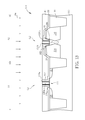
- a second spacer 180 is formed beside the first gate G 1 and the second gate G 2 respectively.
- the second spacer 180 may include an oxide layer 182 located outside first gate G 1 and the second gate G 2 , and a nitride layer 184 located outside the oxide layer 182 , but it is not limited thereto.
- Anion implantation process may be performed to form a source/drain (not shown) in the substrate 110 beside the first gate G 1 and the second gate G 2 respectively.
- a cleaning process P 3 may be performed to clean the surfaces of the first gate G 1 , the second gate G 2 and the substrate 110 , after the second spacer 180 , the source/drain are formed beside the first gate G 1 and the second gate G 2 .
- the cleaning process P 3 may include a pre-cleaning process for forming salicide, such as an ammonia (NH 3 ) and nitrogen trifluoride (NF 3 ) containing cleaning process.
- NH 3 ammonia
- NF 3 nitrogen trifluoride
- the reaction of the ammonia (NH 3 ) and nitrogen trifluoride (NF 3 ) containing cleaning process may be:
- a salicide process may be performed to form a salicide layer 20 in the substrate 110 .
- a protective layer 190 may be selectively formed to entirely cover the first gate G 1 and the second gate G 2 .
- the material of the protective layer 190 is preferably the same as the material of the second spacer 180 , the third cap layer 142 a and the fourth cap layer 142 b , such as a silicon nitride, for being removed together with the nitride layer 184 of the second spacer 180 , the third cap layer 142 a and the fourth cap layer 142 b , but it is not restricted thereto.
- a material layer F is formed to entirely cover the first gate G 1 and the second gate G 2 .
- the material layer F may be a photoresist layer.
- parts of the material layer F, parts of the protective layer 190 , parts of the first gate G 1 and parts of the second gate G 2 are etched back until the third cap layer 142 a and the fourth cap layer 142 b are exposed. At this time, the first cap layer 144 a above the first gate G 1 is removed.
- the method of etching back may include performing an oxygen or fluorine containing dry etching process such as an oxygen plasma dry etching process, but it is not limited thereto.
- the material layer F remaining, the third cap layer 142 a , the fourth cap layer 142 b and the nitride layer 184 of the second spacer 180 are sequentially removed. Due to the protective layer 190 in this embodiment being a silicon nitride layer (the same as the materials of the nitride layer 184 , the third cap layer 142 a and the fourth cap layer 142 b ), it will be removed together with the nitride layer 184 , the third cap layer 142 a can and the fourth cap layer 142 b.
- a contact etch stop layer 30 (CESL) is formed to entirely cover the first gate G 1 and the second gate G 2 , wherein the materials of the contact etch stop layer 30 covering the first gate G 1 and the second gate G 2 may be different, therefore transistors formed by the first gate G 1 and the second gate G 2 (the first gate G 1 may be used to form a PMOS transistor and the second gate G 2 may be used to form an NMOS transistor) can be forced with different stresses.
- the contact etch stop layer 30 may be a single layer contact etch stop layer or a dual contact etch stop layer etc.
- An interdielectric layer 40 is formed to cover the contact etch stop layer 30 .
- a planarization process P 4 such as a chemical mechanical polishing (CMP) process is performed to planarize parts of the interdielectric layer 40 and parts of the contact etch stop layer 30 , until the first gate layer 130 a and the second gate layer 130 b are exposed.
- the contact etch stop layer 30 may include a doped silicon nitride layer, which can force gate channels C 1 and C 2 with stresses; the interdielectric layer 40 may be an oxide layer, but is not limited thereto. Since the material layer F is formed and etched back to make the first gate G 1 and the second gate G 2 have the same height, parts of the interdielectric layer 40 and parts of the contact etch stop layer 30 can be planarized uniformly by the planarization process P 4 . Therefore, the electrical performance and the processing yields of the semiconductor structure 100 being planarized can be improved.
- CMP chemical mechanical polishing
- Some semiconductor processes performed in the following steps such as removing the first gate layer 130 a and the second gate layer 130 b , sequentially filling a barrier layer, a work function metal layer and a main metal electrode layer, etc, are known in the art and are not described herein.
- FIGS. 14-15 schematically depict a cross-sectional view of a static random access memory (SRAM) according to one embodiment.
- FIGS. 16-19 schematically depict a cross-sectional view of a static random access memory (SRAM) according to another embodiment.
- an isolation structure 50 such as a shallow trench isolation structure, is located between an NMOS transistor 220 and a PMOS transistor 240 .
- an epitaxial layer (not shown) is formed in the PMOS transistor 240 , the thickness of a cap layer 242 of the PMOS transistor 240 is lower than the thickness of a cap layer 244 of the NMOS transistor 220 . Therefore, a lithography process is additionally performed to thin the cap layer 244 .
- a photoresist layer 60 formed during the lithography process may be misaligned. If the photoresist layer 60 is shifted to the right, a boundary area B 1 will be etched duplicately. As shown in FIG.
- the thickness of a cap layer 246 in the boundary area B 1 is therefore lower than the thickness of the cap layers 242 and 244 , so an upper part 232 p of a gate layer 232 may be exposed.
- the upper part 232 p being exposed will have salicide formed thereon in following processes, leading to the gate layer 232 being harder to remove or gate layers 232 electrically connecting to each other, giving rise to short circuits.
- the misalignment of the photoresist layer 60 formed during the lithography process may lead to a cap layer 248 and a hard mask layer 250 not being etched because of the photoresist layer 60 covering them.
- the thickness of the cap layer 248 in a boundary B 2 is therefore larger than the thicknesses of the cap layers 242 and 244 , and the hard mask layer 250 for forming the epitaxial layer (not shown) remains on the cap layer 248 .
- FIG. 17 the thickness of the cap layer 248 in a boundary B 2 is therefore larger than the thicknesses of the cap layers 242 and 244 , and the hard mask layer 250 for forming the epitaxial layer (not shown) remains on the cap layer 248 .
- a second spacer 260 that should be formed on a gate 230 , is formed on the hard mask layer 250 because of the hard mask layer 250 residues, wherein the second spacer 260 may include an oxide layer 262 located outside of the hard mask layer 250 , and a nitride layer 264 located outside of the oxide layer 262 .
- the second spacer 260 is removed, part of the hard mask layer 250 not covered by the oxide layer 262 will be etched, which causes notches d 1 and d 2 , and reduces the electrical performances of the static random access memory (SRAM).
- SRAM static random access memory
- the present invention can solve the problem of misalignment in the boundary caused by a lithography process performed twice.
- an etching process is performed to entirely etch the substrate 110 , without using a mask.
- a material for the hard mask layer 250 is a silicon nitride layer, which is different from the materials of the cap layer 242 and the cap layer 244 . Therefore, the static random access memory (SRAM) utilizing the semiconductor process of the present invention will not have said notches d 1 and d 2 , because the hard mask layer 250 can be removed entirely by applying the etching process once.
- the present invention provides the semiconductor process, which forms the cap layer with a material different from the hard mask layer on the gate, so that the hard mask layer (and the spacer formed by the hard mask) can be removed entirely without the cap layer being over-etched, and the gate layer below being exposed.
- the present invention can enhance the efficiency of the contact etch stop layer formed on the gate.
- the hard mask layer can be entirely removed by performing the lithography process once in the present invention, so that the boundary misalignment of the static random access memory (SRAM) can be avoided.
- SRAM static random access memory
- the plurality of the cap layers of the gates having different thicknesses can be removed uniformly in the present invention by the method of forming and etching back the material layer.
- the gates have the same thicknesses and the interdielectric layer and the contact etch stop layer can be planarized uniformly, until the gate layers are exposed by a planarization process, thereby improving the electrical performances of the semiconductor structure.
Abstract
Description
NF3+NH3→NH4F+NH4F.HF
(2) etching (performed at a temperature of 30° C.)
NH4F+NH4F.HF+SiO2→(NH4)2SiF6(s)+H2O
(3) sublimation (performed at a temperature higher than 100° C.)
(NH4)2SiF6(s)→SiF4(g)+NH3(g)
Claims (19)
Priority Applications (1)
| Application Number | Priority Date | Filing Date | Title |
|---|---|---|---|
| US13/304,416 US8709930B2 (en) | 2011-11-25 | 2011-11-25 | Semiconductor process |
Applications Claiming Priority (1)
| Application Number | Priority Date | Filing Date | Title |
|---|---|---|---|
| US13/304,416 US8709930B2 (en) | 2011-11-25 | 2011-11-25 | Semiconductor process |
Publications (2)
| Publication Number | Publication Date |
|---|---|
| US20130137256A1 US20130137256A1 (en) | 2013-05-30 |
| US8709930B2 true US8709930B2 (en) | 2014-04-29 |
Family
ID=48467265
Family Applications (1)
| Application Number | Title | Priority Date | Filing Date |
|---|---|---|---|
| US13/304,416 Active 2032-04-20 US8709930B2 (en) | 2011-11-25 | 2011-11-25 | Semiconductor process |
Country Status (1)
| Country | Link |
|---|---|
| US (1) | US8709930B2 (en) |
Cited By (2)
| Publication number | Priority date | Publication date | Assignee | Title |
|---|---|---|---|---|
| US9536981B1 (en) | 2015-09-29 | 2017-01-03 | International Business Machines Corporation | Field effect transistor device spacers |
| US9548388B1 (en) | 2015-08-04 | 2017-01-17 | International Business Machines Corporation | Forming field effect transistor device spacers |
Families Citing this family (3)
| Publication number | Priority date | Publication date | Assignee | Title |
|---|---|---|---|---|
| US9224656B2 (en) * | 2013-07-25 | 2015-12-29 | Texas Instruments Incorporated | Method of CMOS manufacturing utilizing multi-layer epitaxial hardmask films for improved gate spacer control |
| KR102255174B1 (en) * | 2014-10-10 | 2021-05-24 | 삼성전자주식회사 | Semiconductor device having active region and method of forming the same |
| KR102235612B1 (en) | 2015-01-29 | 2021-04-02 | 삼성전자주식회사 | Semiconductor device having work-function metal and method of forming the same |
Citations (157)
| Publication number | Priority date | Publication date | Assignee | Title |
|---|---|---|---|---|
| US4891303A (en) | 1988-05-26 | 1990-01-02 | Texas Instruments Incorporated | Trilayer microlithographic process using a silicon-based resist as the middle layer |
| US5217910A (en) | 1990-11-05 | 1993-06-08 | Mitsubishi Denki Kabushiki Kaisha | Method of fabricating semiconductor device having sidewall spacers and oblique implantation |
| US5273930A (en) | 1992-09-03 | 1993-12-28 | Motorola, Inc. | Method of forming a non-selective silicon-germanium epitaxial film |
| US5356830A (en) | 1988-09-19 | 1994-10-18 | Kabushiki Kaisha Tobshiba | Semiconductor device and its manufacturing method |
| US5372957A (en) | 1993-07-22 | 1994-12-13 | Taiwan Semiconductor Manufacturing Company | Multiple tilted angle ion implantation MOSFET method |
| US5385630A (en) | 1993-06-29 | 1995-01-31 | Digital Equipment Corporation | Process for increasing sacrificial oxide etch rate to reduce field oxide loss |
| US5399506A (en) | 1992-08-13 | 1995-03-21 | Sony Corporation | Semiconductor fabricating process |
| US5625217A (en) | 1992-12-11 | 1997-04-29 | Intel Corporation | MOS transistor having a composite gate electrode and method of fabrication |
| US5777364A (en) | 1992-11-30 | 1998-07-07 | International Business Machines Corporation | Graded channel field effect transistor |
| US5783479A (en) | 1997-06-23 | 1998-07-21 | National Science Council | Structure and method for manufacturing improved FETs having T-shaped gates |
| US5960322A (en) | 1997-12-19 | 1999-09-28 | Advanced Micro Devices, Inc. | Suppression of boron segregation for shallow source and drain junctions in semiconductors |
| US6030874A (en) | 1997-01-21 | 2000-02-29 | Texas Instruments Incorporated | Doped polysilicon to retard boron diffusion into and through thin gate dielectrics |
| US6033963A (en) | 1999-08-30 | 2000-03-07 | Taiwan Semiconductor Manufacturing Company | Method of forming a metal gate for CMOS devices using a replacement gate process |
| US6048756A (en) | 1997-07-31 | 2000-04-11 | Electronics And Telecommunications Research Institute | Method for making a silicon-on-insulator MOS transistor using a selective SiGe epitaxy |
| US6074954A (en) | 1998-08-31 | 2000-06-13 | Applied Materials, Inc | Process for control of the shape of the etch front in the etching of polysilicon |
| US6100171A (en) | 1998-03-03 | 2000-08-08 | Advanced Micro Devices, Inc. | Reduction of boron penetration by laser anneal removal of fluorine |
| US6110787A (en) | 1999-09-07 | 2000-08-29 | Chartered Semiconductor Manufacturing Ltd. | Method for fabricating a MOS device |
| US6165881A (en) | 1998-10-23 | 2000-12-26 | Taiwan Semiconductor Manufacturing Company | Method of forming salicide poly gate with thin gate oxide and ultra narrow gate width |
| US6165826A (en) | 1994-12-23 | 2000-12-26 | Intel Corporation | Transistor with low resistance tip and method of fabrication in a CMOS process |
| US6191052B1 (en) | 1999-01-25 | 2001-02-20 | Taiwan Semiconductor Manufacturing Company | Method for fabricating an ultra-shallow junction with low resistance using a screen oxide formed by poly re-oxidation in a nitrogen containing atmosphere |
| US6228730B1 (en) | 1999-04-28 | 2001-05-08 | United Microelectronics Corp. | Method of fabricating field effect transistor |
| US6274447B1 (en) | 1996-03-22 | 2001-08-14 | Seiko Epson Corporation | Semiconductor device comprising a MOS element and a fabrication method thereof |
| US6355533B2 (en) | 1999-12-24 | 2002-03-12 | Hyundai Electronics Industries Co., Ltd. | Method for manufacturing semiconductor device |
| US6365476B1 (en) | 2000-10-27 | 2002-04-02 | Ultratech Stepper, Inc. | Laser thermal process for fabricating field-effect transistors |
| US6368926B1 (en) | 2000-03-13 | 2002-04-09 | Advanced Micro Devices, Inc. | Method of forming a semiconductor device with source/drain regions having a deep vertical junction |
| US6444591B1 (en) | 2000-09-30 | 2002-09-03 | Newport Fab, Llc | Method for reducing contamination prior to epitaxial growth and related structure |
| US20020160587A1 (en) | 2001-04-30 | 2002-10-31 | Basanth Jagannathan | Method to increase carbon and boron doping concentrations in Si and SiGe films |
| US20020182423A1 (en) | 2001-04-20 | 2002-12-05 | International Business Machines Corporation | Epitaxial and polycrystalline growth of Si1-x-yGexCy and Si1-yCy alloy layers on Si by UHV-CVD |
| US6537370B1 (en) | 1998-09-10 | 2003-03-25 | FRANCE TéLéCOM | Process for obtaining a layer of single-crystal germanium on a substrate of single-crystal silicon, and products obtained |
| US6544822B2 (en) | 2000-06-21 | 2003-04-08 | Hynix Semiconductor, Inc. | Method for fabricating MOSFET device |
| US6605498B1 (en) | 2002-03-29 | 2003-08-12 | Intel Corporation | Semiconductor transistor having a backfilled channel material |
| US6613695B2 (en) | 2000-11-24 | 2003-09-02 | Asm America, Inc. | Surface preparation prior to deposition |
| US6621131B2 (en) | 2001-11-01 | 2003-09-16 | Intel Corporation | Semiconductor transistor having a stressed channel |
| US6624068B2 (en) | 2001-08-24 | 2003-09-23 | Texas Instruments Incorporated | Polysilicon processing using an anti-reflective dual layer hardmask for 193 nm lithography |
| US20030181005A1 (en) | 2002-03-19 | 2003-09-25 | Kiyota Hachimine | Semiconductor device and a method of manufacturing the same |
| US6632718B1 (en) | 1998-07-15 | 2003-10-14 | Texas Instruments Incorporated | Disposable spacer technology for reduced cost CMOS processing |
| US20030203599A1 (en) | 2000-03-27 | 2003-10-30 | Matsushita Electric Industrial Co. , Ltd. | Semiconductor wafer and method for fabricating the same |
| US6642122B1 (en) | 2002-09-26 | 2003-11-04 | Advanced Micro Devices, Inc. | Dual laser anneal for graded halo profile |
| US6653698B2 (en) | 2001-12-20 | 2003-11-25 | International Business Machines Corporation | Integration of dual workfunction metal gate CMOS devices |
| US6664156B1 (en) | 2002-07-31 | 2003-12-16 | Chartered Semiconductor Manufacturing, Ltd | Method for forming L-shaped spacers with precise width control |
| US6676764B2 (en) | 2001-04-30 | 2004-01-13 | Hynix Semiconductor Inc. | Method for cleaning a substrate in selective epitaxial growth process |
| US6703271B2 (en) | 2001-11-30 | 2004-03-09 | Taiwan Semiconductor Manufacturing Company | Complementary metal oxide semiconductor transistor technology using selective epitaxy of a strained silicon germanium layer |
| US20040045499A1 (en) | 2002-06-10 | 2004-03-11 | Amberwave Systems Corporation | Source and drain elements |
| US20040067631A1 (en) | 2002-10-03 | 2004-04-08 | Haowen Bu | Reduction of seed layer roughness for use in forming SiGe gate electrode |
| US6777275B1 (en) | 2000-11-15 | 2004-08-17 | Advanced Micro Devices, Inc. | Single anneal for dopant activation and silicide formation |
| US6806151B2 (en) | 2001-12-14 | 2004-10-19 | Texas Instruments Incorporated | Methods and apparatus for inducing stress in a semiconductor device |
| US6809402B1 (en) | 2002-08-14 | 2004-10-26 | Advanced Micro Devices, Inc. | Reflowable-doped HDP film |
| US20040227164A1 (en) | 2003-05-14 | 2004-11-18 | Samsung Electronics Co., Ltd. | MOS transistor with elevated source/drain structure and method of fabricating the same |
| US6858483B2 (en) | 2002-12-20 | 2005-02-22 | Intel Corporation | Integrating n-type and p-type metal gate transistors |
| US6858506B2 (en) | 2002-08-08 | 2005-02-22 | Macronix International Co., Ltd. | Method for fabricating locally strained channel |
| US6864135B2 (en) | 2002-10-31 | 2005-03-08 | Freescale Semiconductor, Inc. | Semiconductor fabrication process using transistor spacers of differing widths |
| US6869867B2 (en) | 1997-10-01 | 2005-03-22 | Kabushiki Kaisha Toshiba | Semiconductor device comprising metal silicide films formed to cover gate electrode and source-drain diffusion layers and method of manufacturing the same wherein the silicide on gate is thicker than on source-drain |
| US20050070076A1 (en) | 2001-10-26 | 2005-03-31 | Dion Michel Maurice | Method of depositing high-quality sige on sige substrates |
| US20050079692A1 (en) | 2003-10-10 | 2005-04-14 | Applied Materials, Inc. | Methods to fabricate MOSFET devices using selective deposition process |
| US20050082616A1 (en) | 2003-10-20 | 2005-04-21 | Huajie Chen | High performance stress-enhanced MOSFETs using Si:C and SiGe epitaxial source/drain and method of manufacture |
| US6887751B2 (en) | 2003-09-12 | 2005-05-03 | International Business Machines Corporation | MOSFET performance improvement using deformation in SOI structure |
| US6887762B1 (en) | 1998-11-12 | 2005-05-03 | Intel Corporation | Method of fabricating a field effect transistor structure with abrupt source/drain junctions |
| US6891192B2 (en) | 2003-08-04 | 2005-05-10 | International Business Machines Corporation | Structure and method of making strained semiconductor CMOS transistors having lattice-mismatched semiconductor regions underlying source and drain regions |
| US20050139231A1 (en) | 2003-12-31 | 2005-06-30 | Commissariat A L'energie Atomique | Method of wet cleaning a surface, especially of a material of the silicon-germanium type |
| US6921711B2 (en) | 2003-09-09 | 2005-07-26 | International Business Machines Corporation | Method for forming metal replacement gate of high performance |
| US6930007B2 (en) | 2003-09-15 | 2005-08-16 | Texas Instruments Incorporated | Integration of pre-S/D anneal selective nitride/oxide composite cap for improving transistor performance |
| US6946350B2 (en) | 2003-12-31 | 2005-09-20 | Intel Corporation | Controlled faceting of source/drain regions |
| US6962856B2 (en) | 2002-07-19 | 2005-11-08 | Hynix Semiconductor, Inc. | Method for forming device isolation film of semiconductor device |
| US6967131B2 (en) | 2003-10-29 | 2005-11-22 | International Business Machines Corp. | Field effect transistor with electroplated metal gate |
| US20050260830A1 (en) | 2004-03-25 | 2005-11-24 | Doo-Won Kwon | Methods of fabricating a semiconductor device using a dilute aqueous solution of an ammonia and peroxide mixture |
| US6972461B1 (en) | 2004-06-30 | 2005-12-06 | International Business Machines Corporation | Channel MOSFET with strained silicon channel on strained SiGe |
| US20050285193A1 (en) | 2004-06-28 | 2005-12-29 | Lee Sung-Young | Semiconductor device and method of manufacturing same |
| US20050287752A1 (en) | 2004-06-24 | 2005-12-29 | Applied Materials, Inc. | Methods for forming a transistor |
| US6991979B2 (en) | 2003-09-22 | 2006-01-31 | International Business Machines Corporation | Method for avoiding oxide undercut during pre-silicide clean for thin spacer FETs |
| US6991991B2 (en) | 2003-11-12 | 2006-01-31 | United Microelectronics Corp. | Method for preventing to form a spacer undercut in SEG pre-clean process |
| US20060051922A1 (en) | 2004-09-09 | 2006-03-09 | Taiwan Semiconductor Manufacturing Company, Ltd. | Strained silicon device manufacturing method |
| US20060057859A1 (en) | 2004-09-16 | 2006-03-16 | International Business Machines Corporation | Buffer layer for selective SiGe growth for uniform nucleation |
| US20060076627A1 (en) | 2004-10-12 | 2006-04-13 | International Business Machines Corporation | Ultra shallow junction formation by epitaxial interface limited diffusion |
| US7029966B2 (en) | 2003-09-18 | 2006-04-18 | International Business Machines Corporation | Process options of forming silicided metal gates for advanced CMOS devices |
| US20060088968A1 (en) | 2004-06-17 | 2006-04-27 | Samsung Electronics Co., Ltd. | Methods of fabricating a semiconductor device using a selective epitaxial growth technique |
| US7037773B2 (en) | 2004-03-29 | 2006-05-02 | United Microelectronics Corp. | Method of manufacturing metal-oxide-semiconductor transistor |
| US20060115949A1 (en) | 2004-12-01 | 2006-06-01 | Freescale Semiconductor, Inc. | Semiconductor fabrication process including source/drain recessing and filling |
| US7056794B2 (en) | 2004-01-09 | 2006-06-06 | International Business Machines Corporation | FET gate structure with metal gate electrode and silicide contact |
| US7060579B2 (en) | 2004-07-29 | 2006-06-13 | Texas Instruments Incorporated | Increased drive current by isotropic recess etch |
| US7060576B2 (en) | 2003-10-24 | 2006-06-13 | Intel Corporation | Epitaxially deposited source/drain |
| US7064066B1 (en) | 2004-12-07 | 2006-06-20 | Intel Corporation | Method for making a semiconductor device having a high-k gate dielectric and a titanium carbide gate electrode |
| US7064050B2 (en) | 2003-11-28 | 2006-06-20 | International Business Machines Corporation | Metal carbide gate structure and method of fabrication |
| US7074680B2 (en) | 2004-09-07 | 2006-07-11 | Intel Corporation | Method for making a semiconductor device having a high-k gate dielectric |
| US7112495B2 (en) | 2003-08-15 | 2006-09-26 | Taiwan Semiconductor Manufacturing Company, Ltd. | Structure and method of a strained channel transistor and a second semiconductor component in an integrated circuit |
| US7118952B2 (en) | 2004-07-14 | 2006-10-10 | Taiwan Semiconductor Manufacturing Co., Ltd. | Method of making transistor with strained source/drain |
| US20060228842A1 (en) | 2005-04-07 | 2006-10-12 | Freescale Semiconductor, Inc. | Transistor fabrication using double etch/refill process |
| US20060231826A1 (en) | 2005-04-18 | 2006-10-19 | Toshiba America Electronic Components, Inc. | Step-embedded SiGe structure for PFET mobility enhancement |
| US7126199B2 (en) | 2004-09-27 | 2006-10-24 | Intel Corporation | Multilayer metal gate electrode |
| US20060258126A1 (en) | 2003-02-04 | 2006-11-16 | Sumco Corporation | Semiconductor substrate, field-effect transistor, and their production methods |
| US7148548B2 (en) | 2004-07-20 | 2006-12-12 | Intel Corporation | Semiconductor device with a high-k gate dielectric and a metal gate electrode |
| US20060281288A1 (en) | 2005-06-13 | 2006-12-14 | Fujitsu Limited | Semiconductor device fabrication method |
| US7153734B2 (en) | 2003-12-29 | 2006-12-26 | Intel Corporation | CMOS device with metal and silicide gate electrodes and a method for making it |
| US20060292783A1 (en) | 2005-02-28 | 2006-12-28 | Young-Eun Lee | CMOS transistor and method of manufacturing the same |
| US20060292779A1 (en) | 2004-09-29 | 2006-12-28 | International Business Machines Corporation | Structure and method for making strained channel field effect transistor using sacrificial spacer |
| US7157378B2 (en) | 2004-07-06 | 2007-01-02 | Intel Corporation | Method for making a semiconductor device having a high-k gate dielectric layer and a metal gate electrode |
| US7169675B2 (en) | 2004-07-07 | 2007-01-30 | Chartered Semiconductor Manufacturing, Ltd | Material architecture for the fabrication of low temperature transistor |
| US20070023847A1 (en) | 2005-07-26 | 2007-02-01 | Samsung Electronics Co., Ltd. | Semiconductor device and method of manufacturing the same |
| US20070034906A1 (en) | 2005-08-10 | 2007-02-15 | Taiwan Semiconductor Manufacturing Company, Ltd. | MOS devices with reduced recess on substrate surface |
| US7183596B2 (en) | 2005-06-22 | 2007-02-27 | Taiwan Semiconductor Manufacturing Company, Ltd. | Composite gate structure in an integrated circuit |
| US7183184B2 (en) | 2003-12-29 | 2007-02-27 | Intel Corporation | Method for making a semiconductor device that includes a metal gate electrode |
| US20070049014A1 (en) | 2005-08-25 | 2007-03-01 | Ming-Tsung Chen | Method of performing salicide processes on MOS transistors |
| US20070072376A1 (en) | 2005-09-29 | 2007-03-29 | Semiconductor Manufacturing International (Shanghai) Corporation | Strained-induced mobility enhancement nano-device structure and integrated process architecture for CMOS technologies |
| US20070072353A1 (en) | 2005-09-23 | 2007-03-29 | Chih-Ning Wu | Method of fabricating strained-silicon transistors and strained-silicon CMOS transistors |
| US7202124B2 (en) | 2004-10-01 | 2007-04-10 | Massachusetts Institute Of Technology | Strained gettering layers for semiconductor processes |
| US7217627B2 (en) | 2003-09-18 | 2007-05-15 | Dongbu Electronics Co., Ltd. | Semiconductor devices having diffusion barrier regions and halo implant regions and methods of fabricating the same |
| US7220635B2 (en) | 2003-12-19 | 2007-05-22 | Intel Corporation | Method for making a semiconductor device with a metal gate electrode that is formed on an annealed high-k gate dielectric layer |
| US20070128783A1 (en) | 2005-12-06 | 2007-06-07 | Shyh-Fann Ting | Method for fabricating strained-silicon cmos transistors |
| US20070166929A1 (en) | 2006-01-18 | 2007-07-19 | Sumco Corporation | Method of producing semiconductor wafer |
| US7288822B1 (en) | 2006-04-07 | 2007-10-30 | United Microelectronics Corp. | Semiconductor structure and fabricating method thereof |
| US20070262396A1 (en) | 2006-04-25 | 2007-11-15 | International Business Machines Corporation | Transistors Having V-shape Source/Drain Metal Contacts |
| US20070262451A1 (en) | 2006-05-09 | 2007-11-15 | Willy Rachmady | Recessed workfunction metal in CMOS transistor gates |
| US7303999B1 (en) | 2005-12-13 | 2007-12-04 | Lam Research Corporation | Multi-step method for etching strain gate recesses |
| US20080014688A1 (en) | 2006-07-06 | 2008-01-17 | Voon-Yew Thean | Selective uniaxial stress modification for use with strained silicon on insulator integrated circuit |
| US7335959B2 (en) | 2005-01-06 | 2008-02-26 | Intel Corporation | Device with stepped source/drain region profile |
| US20080061366A1 (en) | 2006-09-11 | 2008-03-13 | United Microelectronics Corp. | Complementary metal-oxide-semiconductor device and fabricating method thereof |
| US20080067545A1 (en) | 2006-09-20 | 2008-03-20 | Samsung Electronics Co., Ltd | Semiconductor device including field effect transistor and method of forming the same |
| US20080076236A1 (en) | 2006-09-21 | 2008-03-27 | Jih-Shun Chiang | Method for forming silicon-germanium epitaxial layer |
| US7355281B2 (en) | 2004-04-20 | 2008-04-08 | Intel Corporation | Method for making semiconductor device having a high-k gate dielectric layer and a metal gate electrode |
| US20080085577A1 (en) | 2006-10-05 | 2008-04-10 | Hung-Lin Shih | Method of manufacturing complementary metal oxide semiconductor transistor |
| US20080116525A1 (en) | 2006-11-16 | 2008-05-22 | United Microelectronics Corp. | Complementary metal-oxide-semiconductor device |
| US20080124874A1 (en) | 2006-11-03 | 2008-05-29 | Samsung Electronics Co., Ltd. | Methods of Forming Field Effect Transistors Having Silicon-Germanium Source and Drain Regions |
| US20080128746A1 (en) | 2006-12-05 | 2008-06-05 | Yin-Pin Wang | Dual-SiGe epitaxy for MOS devices |
| US20080142886A1 (en) | 2006-12-18 | 2008-06-19 | Chin-I Liao | Treatment method of semiconductor, method for manufacturing mos, and mos structure |
| US7390709B2 (en) | 2004-09-08 | 2008-06-24 | Intel Corporation | Method for making a semiconductor device having a high-k gate dielectric layer and a metal gate electrode |
| US7410859B1 (en) | 2005-11-07 | 2008-08-12 | Advanced Micro Devices, Inc. | Stressed MOS device and method for its fabrication |
| US20080220579A1 (en) | 2007-03-07 | 2008-09-11 | Advanced Micro Devices, Inc. | Stress enhanced mos transistor and methods for its fabrication |
| US20080233746A1 (en) | 2007-03-21 | 2008-09-25 | Hui-Ling Huang | Method for manufacturing mos transistors utilizing a hybrid hard mask |
| US20080233722A1 (en) | 2007-03-23 | 2008-09-25 | United Microelectronics Corp. | Method of forming selective area compound semiconductor epitaxial layer |
| US7462239B2 (en) | 2001-05-30 | 2008-12-09 | Asm America, Inc. | Low temperature load and bake |
| US20090039433A1 (en) | 2007-08-08 | 2009-02-12 | Taiwan Semiconductor Manufacturing Company, Ltd. | Semiconductor device with high-k/dual metal gate |
| US20090039389A1 (en) | 2007-08-09 | 2009-02-12 | Chu-Yin Tseng | Method of fabricating metal oxide semiconductor transistor |
| US20090045456A1 (en) | 2007-08-13 | 2009-02-19 | United Microelectronics Corp. | Semiconductor device and method of fabricating the same |
| US7494858B2 (en) | 2005-06-30 | 2009-02-24 | Intel Corporation | Transistor with improved tip profile and method of manufacture thereof |
| US7494856B2 (en) | 2006-03-30 | 2009-02-24 | Freescale Semiconductor, Inc. | Semiconductor fabrication process using etch stop layer to optimize formation of source/drain stressor |
| US20090057769A1 (en) | 2007-08-31 | 2009-03-05 | Andy Wei | Cmos device having gate insulation layers of different type and thickness and a method of forming the same |
| US20090095992A1 (en) | 2006-12-22 | 2009-04-16 | Tomoya Sanuki | Semiconductor device including mos field effect transistor and method for manufacturing the semiconductor device |
| US20090117715A1 (en) | 2006-02-27 | 2009-05-07 | Fujitsu Limited | Semiconductor device fabricated by selective epitaxial growth method |
| US20090124056A1 (en) | 2007-11-12 | 2009-05-14 | United Microelectronics Corp. | Method of fabricating semiconductor device |
| US20090166625A1 (en) | 2007-12-28 | 2009-07-02 | United Microelectronics Corp. | Mos device structure |
| US20090186458A1 (en) | 2008-01-23 | 2009-07-23 | Chih-Hao Yu | Method for manufacturing a cmos device having dual metal gate |
| US20090186475A1 (en) | 2008-01-21 | 2009-07-23 | Shyh-Fann Ting | Method of manufacturing a MOS transistor |
| US20090184402A1 (en) | 2008-01-22 | 2009-07-23 | United Microelectronics Corp. | Method of fabricating a shallow trench isolation structure including forming a second liner covering the corner of the trench and first liner. |
| US7592231B2 (en) | 2006-08-01 | 2009-09-22 | United Microelectronics Corp. | MOS transistor and fabrication thereof |
| US20090246922A1 (en) | 2008-03-27 | 2009-10-01 | Meng-Yi Wu | Method of forming cmos transistor |
| US20090278170A1 (en) | 2008-05-07 | 2009-11-12 | Yun-Chi Yang | Semiconductor device and manufacturing method thereof |
| US7622344B2 (en) | 2007-07-17 | 2009-11-24 | United Microelectronics Corp. | Method of manufacturing complementary metal oxide semiconductor transistors |
| US20090302348A1 (en) | 2008-06-10 | 2009-12-10 | International Business Machines Corporation | Stress enhanced transistor devices and methods of making |
| US20100001317A1 (en) | 2008-07-03 | 2010-01-07 | Yi-Wei Chen | Cmos transistor and the method for manufacturing the same |
| US7667227B2 (en) | 2004-12-28 | 2010-02-23 | Fujitsu Microelectronics Limited | Semiconductor device and fabrication method thereof |
| US20100052066A1 (en) | 2008-08-26 | 2010-03-04 | Taiwan Semiconductor Manufacturing Company, Ltd. | structure and method for a cmos device with doped conducting metal oxide as the gate electrode |
| US20100065926A1 (en) | 2008-09-12 | 2010-03-18 | Taiwan Semiconductor Manufacturing Company, Ltd. | Photoresist etch back method for gate last process |
| US20100068877A1 (en) | 2008-09-12 | 2010-03-18 | Taiwan Semiconductor Manufacturing Company, Ltd. | Method for tuning a work function of high-k metal gate devices |
| US7691752B2 (en) | 2007-03-30 | 2010-04-06 | Intel Corporation | Methods of forming improved EPI fill on narrow isolation bounded source/drain regions and structures formed thereby |
| US20100093147A1 (en) | 2008-10-14 | 2010-04-15 | Chin-I Liao | Method for forming a semiconductor device |
| US7838370B2 (en) | 2006-12-27 | 2010-11-23 | Texas Instruments Incorporated | Highly selective liners for semiconductor fabrication |
| US20120012938A1 (en) * | 2010-07-16 | 2012-01-19 | Chun-Chia Chen | Method of manufacturing complementary metal oxide semiconductor device |
| US20120153398A1 (en) * | 2010-12-21 | 2012-06-21 | Globalfoundries Inc. | Encapsulation of Closely Spaced Gate Electrode Structures |
-
2011
- 2011-11-25 US US13/304,416 patent/US8709930B2/en active Active
Patent Citations (170)
| Publication number | Priority date | Publication date | Assignee | Title |
|---|---|---|---|---|
| US4891303A (en) | 1988-05-26 | 1990-01-02 | Texas Instruments Incorporated | Trilayer microlithographic process using a silicon-based resist as the middle layer |
| US5356830A (en) | 1988-09-19 | 1994-10-18 | Kabushiki Kaisha Tobshiba | Semiconductor device and its manufacturing method |
| US5217910A (en) | 1990-11-05 | 1993-06-08 | Mitsubishi Denki Kabushiki Kaisha | Method of fabricating semiconductor device having sidewall spacers and oblique implantation |
| US5399506A (en) | 1992-08-13 | 1995-03-21 | Sony Corporation | Semiconductor fabricating process |
| US5273930A (en) | 1992-09-03 | 1993-12-28 | Motorola, Inc. | Method of forming a non-selective silicon-germanium epitaxial film |
| US5777364A (en) | 1992-11-30 | 1998-07-07 | International Business Machines Corporation | Graded channel field effect transistor |
| US5783478A (en) | 1992-12-11 | 1998-07-21 | Intel Corporation | Method of frabricating a MOS transistor having a composite gate electrode |
| US5625217A (en) | 1992-12-11 | 1997-04-29 | Intel Corporation | MOS transistor having a composite gate electrode and method of fabrication |
| US5385630A (en) | 1993-06-29 | 1995-01-31 | Digital Equipment Corporation | Process for increasing sacrificial oxide etch rate to reduce field oxide loss |
| US5372957A (en) | 1993-07-22 | 1994-12-13 | Taiwan Semiconductor Manufacturing Company | Multiple tilted angle ion implantation MOSFET method |
| US6165826A (en) | 1994-12-23 | 2000-12-26 | Intel Corporation | Transistor with low resistance tip and method of fabrication in a CMOS process |
| US6274447B1 (en) | 1996-03-22 | 2001-08-14 | Seiko Epson Corporation | Semiconductor device comprising a MOS element and a fabrication method thereof |
| US6030874A (en) | 1997-01-21 | 2000-02-29 | Texas Instruments Incorporated | Doped polysilicon to retard boron diffusion into and through thin gate dielectrics |
| US5783479A (en) | 1997-06-23 | 1998-07-21 | National Science Council | Structure and method for manufacturing improved FETs having T-shaped gates |
| US6048756A (en) | 1997-07-31 | 2000-04-11 | Electronics And Telecommunications Research Institute | Method for making a silicon-on-insulator MOS transistor using a selective SiGe epitaxy |
| US6869867B2 (en) | 1997-10-01 | 2005-03-22 | Kabushiki Kaisha Toshiba | Semiconductor device comprising metal silicide films formed to cover gate electrode and source-drain diffusion layers and method of manufacturing the same wherein the silicide on gate is thicker than on source-drain |
| US5960322A (en) | 1997-12-19 | 1999-09-28 | Advanced Micro Devices, Inc. | Suppression of boron segregation for shallow source and drain junctions in semiconductors |
| US6100171A (en) | 1998-03-03 | 2000-08-08 | Advanced Micro Devices, Inc. | Reduction of boron penetration by laser anneal removal of fluorine |
| US6699763B2 (en) | 1998-07-15 | 2004-03-02 | Texas Instruments Incorporated | Disposable spacer technology for reduced cost CMOS processing |
| US6632718B1 (en) | 1998-07-15 | 2003-10-14 | Texas Instruments Incorporated | Disposable spacer technology for reduced cost CMOS processing |
| US6074954A (en) | 1998-08-31 | 2000-06-13 | Applied Materials, Inc | Process for control of the shape of the etch front in the etching of polysilicon |
| US6537370B1 (en) | 1998-09-10 | 2003-03-25 | FRANCE TéLéCOM | Process for obtaining a layer of single-crystal germanium on a substrate of single-crystal silicon, and products obtained |
| US6165881A (en) | 1998-10-23 | 2000-12-26 | Taiwan Semiconductor Manufacturing Company | Method of forming salicide poly gate with thin gate oxide and ultra narrow gate width |
| US6887762B1 (en) | 1998-11-12 | 2005-05-03 | Intel Corporation | Method of fabricating a field effect transistor structure with abrupt source/drain junctions |
| US6191052B1 (en) | 1999-01-25 | 2001-02-20 | Taiwan Semiconductor Manufacturing Company | Method for fabricating an ultra-shallow junction with low resistance using a screen oxide formed by poly re-oxidation in a nitrogen containing atmosphere |
| US6228730B1 (en) | 1999-04-28 | 2001-05-08 | United Microelectronics Corp. | Method of fabricating field effect transistor |
| US6033963A (en) | 1999-08-30 | 2000-03-07 | Taiwan Semiconductor Manufacturing Company | Method of forming a metal gate for CMOS devices using a replacement gate process |
| US6110787A (en) | 1999-09-07 | 2000-08-29 | Chartered Semiconductor Manufacturing Ltd. | Method for fabricating a MOS device |
| US6355533B2 (en) | 1999-12-24 | 2002-03-12 | Hyundai Electronics Industries Co., Ltd. | Method for manufacturing semiconductor device |
| US6368926B1 (en) | 2000-03-13 | 2002-04-09 | Advanced Micro Devices, Inc. | Method of forming a semiconductor device with source/drain regions having a deep vertical junction |
| US20030203599A1 (en) | 2000-03-27 | 2003-10-30 | Matsushita Electric Industrial Co. , Ltd. | Semiconductor wafer and method for fabricating the same |
| US6544822B2 (en) | 2000-06-21 | 2003-04-08 | Hynix Semiconductor, Inc. | Method for fabricating MOSFET device |
| US6444591B1 (en) | 2000-09-30 | 2002-09-03 | Newport Fab, Llc | Method for reducing contamination prior to epitaxial growth and related structure |
| US6365476B1 (en) | 2000-10-27 | 2002-04-02 | Ultratech Stepper, Inc. | Laser thermal process for fabricating field-effect transistors |
| US6777275B1 (en) | 2000-11-15 | 2004-08-17 | Advanced Micro Devices, Inc. | Single anneal for dopant activation and silicide formation |
| US6613695B2 (en) | 2000-11-24 | 2003-09-02 | Asm America, Inc. | Surface preparation prior to deposition |
| US20020182423A1 (en) | 2001-04-20 | 2002-12-05 | International Business Machines Corporation | Epitaxial and polycrystalline growth of Si1-x-yGexCy and Si1-yCy alloy layers on Si by UHV-CVD |
| US6676764B2 (en) | 2001-04-30 | 2004-01-13 | Hynix Semiconductor Inc. | Method for cleaning a substrate in selective epitaxial growth process |
| US20020160587A1 (en) | 2001-04-30 | 2002-10-31 | Basanth Jagannathan | Method to increase carbon and boron doping concentrations in Si and SiGe films |
| US7462239B2 (en) | 2001-05-30 | 2008-12-09 | Asm America, Inc. | Low temperature load and bake |
| US6624068B2 (en) | 2001-08-24 | 2003-09-23 | Texas Instruments Incorporated | Polysilicon processing using an anti-reflective dual layer hardmask for 193 nm lithography |
| US20050070076A1 (en) | 2001-10-26 | 2005-03-31 | Dion Michel Maurice | Method of depositing high-quality sige on sige substrates |
| US6861318B2 (en) | 2001-11-01 | 2005-03-01 | Intel Corporation | Semiconductor transistor having a stressed channel |
| US6621131B2 (en) | 2001-11-01 | 2003-09-16 | Intel Corporation | Semiconductor transistor having a stressed channel |
| US6703271B2 (en) | 2001-11-30 | 2004-03-09 | Taiwan Semiconductor Manufacturing Company | Complementary metal oxide semiconductor transistor technology using selective epitaxy of a strained silicon germanium layer |
| US6806151B2 (en) | 2001-12-14 | 2004-10-19 | Texas Instruments Incorporated | Methods and apparatus for inducing stress in a semiconductor device |
| US6653698B2 (en) | 2001-12-20 | 2003-11-25 | International Business Machines Corporation | Integration of dual workfunction metal gate CMOS devices |
| US20030181005A1 (en) | 2002-03-19 | 2003-09-25 | Kiyota Hachimine | Semiconductor device and a method of manufacturing the same |
| US6605498B1 (en) | 2002-03-29 | 2003-08-12 | Intel Corporation | Semiconductor transistor having a backfilled channel material |
| US20040045499A1 (en) | 2002-06-10 | 2004-03-11 | Amberwave Systems Corporation | Source and drain elements |
| US6962856B2 (en) | 2002-07-19 | 2005-11-08 | Hynix Semiconductor, Inc. | Method for forming device isolation film of semiconductor device |
| US6664156B1 (en) | 2002-07-31 | 2003-12-16 | Chartered Semiconductor Manufacturing, Ltd | Method for forming L-shaped spacers with precise width control |
| US6858506B2 (en) | 2002-08-08 | 2005-02-22 | Macronix International Co., Ltd. | Method for fabricating locally strained channel |
| US6809402B1 (en) | 2002-08-14 | 2004-10-26 | Advanced Micro Devices, Inc. | Reflowable-doped HDP film |
| US6642122B1 (en) | 2002-09-26 | 2003-11-04 | Advanced Micro Devices, Inc. | Dual laser anneal for graded halo profile |
| US20040067631A1 (en) | 2002-10-03 | 2004-04-08 | Haowen Bu | Reduction of seed layer roughness for use in forming SiGe gate electrode |
| US6864135B2 (en) | 2002-10-31 | 2005-03-08 | Freescale Semiconductor, Inc. | Semiconductor fabrication process using transistor spacers of differing widths |
| US6953719B2 (en) | 2002-12-20 | 2005-10-11 | Intel Corporation | Integrating n-type and p-type metal gate transistors |
| US6858483B2 (en) | 2002-12-20 | 2005-02-22 | Intel Corporation | Integrating n-type and p-type metal gate transistors |
| US6972225B2 (en) | 2002-12-20 | 2005-12-06 | Intel Corporation | integrating n-type and P-type metal gate transistors |
| US7316949B2 (en) | 2002-12-20 | 2008-01-08 | Intel Corporation | Integrating n-type and p-type metal gate transistors |
| US20060258126A1 (en) | 2003-02-04 | 2006-11-16 | Sumco Corporation | Semiconductor substrate, field-effect transistor, and their production methods |
| US20040227164A1 (en) | 2003-05-14 | 2004-11-18 | Samsung Electronics Co., Ltd. | MOS transistor with elevated source/drain structure and method of fabricating the same |
| US20060163558A1 (en) | 2003-05-14 | 2006-07-27 | Samsung Electronics, Co., Ltd. | MOS transistor with elevated source/drain structure |
| US6891192B2 (en) | 2003-08-04 | 2005-05-10 | International Business Machines Corporation | Structure and method of making strained semiconductor CMOS transistors having lattice-mismatched semiconductor regions underlying source and drain regions |
| US7112495B2 (en) | 2003-08-15 | 2006-09-26 | Taiwan Semiconductor Manufacturing Company, Ltd. | Structure and method of a strained channel transistor and a second semiconductor component in an integrated circuit |
| US6921711B2 (en) | 2003-09-09 | 2005-07-26 | International Business Machines Corporation | Method for forming metal replacement gate of high performance |
| US6887751B2 (en) | 2003-09-12 | 2005-05-03 | International Business Machines Corporation | MOSFET performance improvement using deformation in SOI structure |
| US6930007B2 (en) | 2003-09-15 | 2005-08-16 | Texas Instruments Incorporated | Integration of pre-S/D anneal selective nitride/oxide composite cap for improving transistor performance |
| US7217627B2 (en) | 2003-09-18 | 2007-05-15 | Dongbu Electronics Co., Ltd. | Semiconductor devices having diffusion barrier regions and halo implant regions and methods of fabricating the same |
| US7326610B2 (en) | 2003-09-18 | 2008-02-05 | International Business Machines Corporation | Process options of forming silicided metal gates for advanced CMOS devices |
| US7029966B2 (en) | 2003-09-18 | 2006-04-18 | International Business Machines Corporation | Process options of forming silicided metal gates for advanced CMOS devices |
| US6991979B2 (en) | 2003-09-22 | 2006-01-31 | International Business Machines Corporation | Method for avoiding oxide undercut during pre-silicide clean for thin spacer FETs |
| US20050079692A1 (en) | 2003-10-10 | 2005-04-14 | Applied Materials, Inc. | Methods to fabricate MOSFET devices using selective deposition process |
| US7132338B2 (en) | 2003-10-10 | 2006-11-07 | Applied Materials, Inc. | Methods to fabricate MOSFET devices using selective deposition process |
| US20070082451A1 (en) | 2003-10-10 | 2007-04-12 | Samoilov Arkadii V | Methods to fabricate mosfet devices using a selective deposition process |
| US20050082616A1 (en) | 2003-10-20 | 2005-04-21 | Huajie Chen | High performance stress-enhanced MOSFETs using Si:C and SiGe epitaxial source/drain and method of manufacture |
| US7060576B2 (en) | 2003-10-24 | 2006-06-13 | Intel Corporation | Epitaxially deposited source/drain |
| US7112851B2 (en) | 2003-10-29 | 2006-09-26 | International Business Machines Corporation | Field effect transistor with electroplated metal gate |
| US6967131B2 (en) | 2003-10-29 | 2005-11-22 | International Business Machines Corp. | Field effect transistor with electroplated metal gate |
| US6991991B2 (en) | 2003-11-12 | 2006-01-31 | United Microelectronics Corp. | Method for preventing to form a spacer undercut in SEG pre-clean process |
| US7064050B2 (en) | 2003-11-28 | 2006-06-20 | International Business Machines Corporation | Metal carbide gate structure and method of fabrication |
| US7220635B2 (en) | 2003-12-19 | 2007-05-22 | Intel Corporation | Method for making a semiconductor device with a metal gate electrode that is formed on an annealed high-k gate dielectric layer |
| US7183184B2 (en) | 2003-12-29 | 2007-02-27 | Intel Corporation | Method for making a semiconductor device that includes a metal gate electrode |
| US7153734B2 (en) | 2003-12-29 | 2006-12-26 | Intel Corporation | CMOS device with metal and silicide gate electrodes and a method for making it |
| US6946350B2 (en) | 2003-12-31 | 2005-09-20 | Intel Corporation | Controlled faceting of source/drain regions |
| US20050139231A1 (en) | 2003-12-31 | 2005-06-30 | Commissariat A L'energie Atomique | Method of wet cleaning a surface, especially of a material of the silicon-germanium type |
| US7056794B2 (en) | 2004-01-09 | 2006-06-06 | International Business Machines Corporation | FET gate structure with metal gate electrode and silicide contact |
| US20050260830A1 (en) | 2004-03-25 | 2005-11-24 | Doo-Won Kwon | Methods of fabricating a semiconductor device using a dilute aqueous solution of an ammonia and peroxide mixture |
| US7037773B2 (en) | 2004-03-29 | 2006-05-02 | United Microelectronics Corp. | Method of manufacturing metal-oxide-semiconductor transistor |
| US7355281B2 (en) | 2004-04-20 | 2008-04-08 | Intel Corporation | Method for making semiconductor device having a high-k gate dielectric layer and a metal gate electrode |
| US20060088968A1 (en) | 2004-06-17 | 2006-04-27 | Samsung Electronics Co., Ltd. | Methods of fabricating a semiconductor device using a selective epitaxial growth technique |
| US20050287752A1 (en) | 2004-06-24 | 2005-12-29 | Applied Materials, Inc. | Methods for forming a transistor |
| US20050285193A1 (en) | 2004-06-28 | 2005-12-29 | Lee Sung-Young | Semiconductor device and method of manufacturing same |
| US6972461B1 (en) | 2004-06-30 | 2005-12-06 | International Business Machines Corporation | Channel MOSFET with strained silicon channel on strained SiGe |
| US7157378B2 (en) | 2004-07-06 | 2007-01-02 | Intel Corporation | Method for making a semiconductor device having a high-k gate dielectric layer and a metal gate electrode |
| US7169675B2 (en) | 2004-07-07 | 2007-01-30 | Chartered Semiconductor Manufacturing, Ltd | Material architecture for the fabrication of low temperature transistor |
| US7118952B2 (en) | 2004-07-14 | 2006-10-10 | Taiwan Semiconductor Manufacturing Co., Ltd. | Method of making transistor with strained source/drain |
| US7148548B2 (en) | 2004-07-20 | 2006-12-12 | Intel Corporation | Semiconductor device with a high-k gate dielectric and a metal gate electrode |
| US7060579B2 (en) | 2004-07-29 | 2006-06-13 | Texas Instruments Incorporated | Increased drive current by isotropic recess etch |
| US7074680B2 (en) | 2004-09-07 | 2006-07-11 | Intel Corporation | Method for making a semiconductor device having a high-k gate dielectric |
| US7390709B2 (en) | 2004-09-08 | 2008-06-24 | Intel Corporation | Method for making a semiconductor device having a high-k gate dielectric layer and a metal gate electrode |
| US20060051922A1 (en) | 2004-09-09 | 2006-03-09 | Taiwan Semiconductor Manufacturing Company, Ltd. | Strained silicon device manufacturing method |
| US20060057859A1 (en) | 2004-09-16 | 2006-03-16 | International Business Machines Corporation | Buffer layer for selective SiGe growth for uniform nucleation |
| US7126199B2 (en) | 2004-09-27 | 2006-10-24 | Intel Corporation | Multilayer metal gate electrode |
| US20060292779A1 (en) | 2004-09-29 | 2006-12-28 | International Business Machines Corporation | Structure and method for making strained channel field effect transistor using sacrificial spacer |
| US7202124B2 (en) | 2004-10-01 | 2007-04-10 | Massachusetts Institute Of Technology | Strained gettering layers for semiconductor processes |
| US20060076627A1 (en) | 2004-10-12 | 2006-04-13 | International Business Machines Corporation | Ultra shallow junction formation by epitaxial interface limited diffusion |
| US20060115949A1 (en) | 2004-12-01 | 2006-06-01 | Freescale Semiconductor, Inc. | Semiconductor fabrication process including source/drain recessing and filling |
| US7317231B2 (en) | 2004-12-07 | 2008-01-08 | Intel Corporation | Method for making a semiconductor device having a high-K gate dielectric and a titanium carbide gate electrode |
| US7064066B1 (en) | 2004-12-07 | 2006-06-20 | Intel Corporation | Method for making a semiconductor device having a high-k gate dielectric and a titanium carbide gate electrode |
| US7667227B2 (en) | 2004-12-28 | 2010-02-23 | Fujitsu Microelectronics Limited | Semiconductor device and fabrication method thereof |
| US7335959B2 (en) | 2005-01-06 | 2008-02-26 | Intel Corporation | Device with stepped source/drain region profile |
| US20060292783A1 (en) | 2005-02-28 | 2006-12-28 | Young-Eun Lee | CMOS transistor and method of manufacturing the same |
| US20060228842A1 (en) | 2005-04-07 | 2006-10-12 | Freescale Semiconductor, Inc. | Transistor fabrication using double etch/refill process |
| US20060231826A1 (en) | 2005-04-18 | 2006-10-19 | Toshiba America Electronic Components, Inc. | Step-embedded SiGe structure for PFET mobility enhancement |
| US20060281288A1 (en) | 2005-06-13 | 2006-12-14 | Fujitsu Limited | Semiconductor device fabrication method |
| US7183596B2 (en) | 2005-06-22 | 2007-02-27 | Taiwan Semiconductor Manufacturing Company, Ltd. | Composite gate structure in an integrated circuit |
| US7494858B2 (en) | 2005-06-30 | 2009-02-24 | Intel Corporation | Transistor with improved tip profile and method of manufacture thereof |
| US20070023847A1 (en) | 2005-07-26 | 2007-02-01 | Samsung Electronics Co., Ltd. | Semiconductor device and method of manufacturing the same |
| US20070034906A1 (en) | 2005-08-10 | 2007-02-15 | Taiwan Semiconductor Manufacturing Company, Ltd. | MOS devices with reduced recess on substrate surface |
| US20070049014A1 (en) | 2005-08-25 | 2007-03-01 | Ming-Tsung Chen | Method of performing salicide processes on MOS transistors |
| US7491615B2 (en) | 2005-09-23 | 2009-02-17 | United Microelectronics Corp. | Method of fabricating strained-silicon transistors and strained-silicon CMOS transistors |
| US20070072353A1 (en) | 2005-09-23 | 2007-03-29 | Chih-Ning Wu | Method of fabricating strained-silicon transistors and strained-silicon CMOS transistors |
| US20070072376A1 (en) | 2005-09-29 | 2007-03-29 | Semiconductor Manufacturing International (Shanghai) Corporation | Strained-induced mobility enhancement nano-device structure and integrated process architecture for CMOS technologies |
| US7410859B1 (en) | 2005-11-07 | 2008-08-12 | Advanced Micro Devices, Inc. | Stressed MOS device and method for its fabrication |
| US20070128783A1 (en) | 2005-12-06 | 2007-06-07 | Shyh-Fann Ting | Method for fabricating strained-silicon cmos transistors |
| US7303999B1 (en) | 2005-12-13 | 2007-12-04 | Lam Research Corporation | Multi-step method for etching strain gate recesses |
| US20070166929A1 (en) | 2006-01-18 | 2007-07-19 | Sumco Corporation | Method of producing semiconductor wafer |
| US20090117715A1 (en) | 2006-02-27 | 2009-05-07 | Fujitsu Limited | Semiconductor device fabricated by selective epitaxial growth method |
| US7494856B2 (en) | 2006-03-30 | 2009-02-24 | Freescale Semiconductor, Inc. | Semiconductor fabrication process using etch stop layer to optimize formation of source/drain stressor |
| US7288822B1 (en) | 2006-04-07 | 2007-10-30 | United Microelectronics Corp. | Semiconductor structure and fabricating method thereof |
| US20070262396A1 (en) | 2006-04-25 | 2007-11-15 | International Business Machines Corporation | Transistors Having V-shape Source/Drain Metal Contacts |
| US20070262451A1 (en) | 2006-05-09 | 2007-11-15 | Willy Rachmady | Recessed workfunction metal in CMOS transistor gates |
| US20080014688A1 (en) | 2006-07-06 | 2008-01-17 | Voon-Yew Thean | Selective uniaxial stress modification for use with strained silicon on insulator integrated circuit |
| US7592231B2 (en) | 2006-08-01 | 2009-09-22 | United Microelectronics Corp. | MOS transistor and fabrication thereof |
| US20080061366A1 (en) | 2006-09-11 | 2008-03-13 | United Microelectronics Corp. | Complementary metal-oxide-semiconductor device and fabricating method thereof |
| US20080067545A1 (en) | 2006-09-20 | 2008-03-20 | Samsung Electronics Co., Ltd | Semiconductor device including field effect transistor and method of forming the same |
| US20080076236A1 (en) | 2006-09-21 | 2008-03-27 | Jih-Shun Chiang | Method for forming silicon-germanium epitaxial layer |
| US20080085577A1 (en) | 2006-10-05 | 2008-04-10 | Hung-Lin Shih | Method of manufacturing complementary metal oxide semiconductor transistor |
| US20080124874A1 (en) | 2006-11-03 | 2008-05-29 | Samsung Electronics Co., Ltd. | Methods of Forming Field Effect Transistors Having Silicon-Germanium Source and Drain Regions |
| US20080116525A1 (en) | 2006-11-16 | 2008-05-22 | United Microelectronics Corp. | Complementary metal-oxide-semiconductor device |
| US20080128746A1 (en) | 2006-12-05 | 2008-06-05 | Yin-Pin Wang | Dual-SiGe epitaxy for MOS devices |
| US20080142886A1 (en) | 2006-12-18 | 2008-06-19 | Chin-I Liao | Treatment method of semiconductor, method for manufacturing mos, and mos structure |
| US20090095992A1 (en) | 2006-12-22 | 2009-04-16 | Tomoya Sanuki | Semiconductor device including mos field effect transistor and method for manufacturing the semiconductor device |
| US7838370B2 (en) | 2006-12-27 | 2010-11-23 | Texas Instruments Incorporated | Highly selective liners for semiconductor fabrication |
| US20080220579A1 (en) | 2007-03-07 | 2008-09-11 | Advanced Micro Devices, Inc. | Stress enhanced mos transistor and methods for its fabrication |
| US20080233746A1 (en) | 2007-03-21 | 2008-09-25 | Hui-Ling Huang | Method for manufacturing mos transistors utilizing a hybrid hard mask |
| US20080233722A1 (en) | 2007-03-23 | 2008-09-25 | United Microelectronics Corp. | Method of forming selective area compound semiconductor epitaxial layer |
| US7691752B2 (en) | 2007-03-30 | 2010-04-06 | Intel Corporation | Methods of forming improved EPI fill on narrow isolation bounded source/drain regions and structures formed thereby |
| US7622344B2 (en) | 2007-07-17 | 2009-11-24 | United Microelectronics Corp. | Method of manufacturing complementary metal oxide semiconductor transistors |
| US20090039433A1 (en) | 2007-08-08 | 2009-02-12 | Taiwan Semiconductor Manufacturing Company, Ltd. | Semiconductor device with high-k/dual metal gate |
| US20090039389A1 (en) | 2007-08-09 | 2009-02-12 | Chu-Yin Tseng | Method of fabricating metal oxide semiconductor transistor |
| US20090045456A1 (en) | 2007-08-13 | 2009-02-19 | United Microelectronics Corp. | Semiconductor device and method of fabricating the same |
| US20090057769A1 (en) | 2007-08-31 | 2009-03-05 | Andy Wei | Cmos device having gate insulation layers of different type and thickness and a method of forming the same |
| US20090124056A1 (en) | 2007-11-12 | 2009-05-14 | United Microelectronics Corp. | Method of fabricating semiconductor device |
| US20090166625A1 (en) | 2007-12-28 | 2009-07-02 | United Microelectronics Corp. | Mos device structure |
| US20090186475A1 (en) | 2008-01-21 | 2009-07-23 | Shyh-Fann Ting | Method of manufacturing a MOS transistor |
| US20090184402A1 (en) | 2008-01-22 | 2009-07-23 | United Microelectronics Corp. | Method of fabricating a shallow trench isolation structure including forming a second liner covering the corner of the trench and first liner. |
| US20090186458A1 (en) | 2008-01-23 | 2009-07-23 | Chih-Hao Yu | Method for manufacturing a cmos device having dual metal gate |
| US20090246922A1 (en) | 2008-03-27 | 2009-10-01 | Meng-Yi Wu | Method of forming cmos transistor |
| US20090278170A1 (en) | 2008-05-07 | 2009-11-12 | Yun-Chi Yang | Semiconductor device and manufacturing method thereof |
| US20090302348A1 (en) | 2008-06-10 | 2009-12-10 | International Business Machines Corporation | Stress enhanced transistor devices and methods of making |
| US20100001317A1 (en) | 2008-07-03 | 2010-01-07 | Yi-Wei Chen | Cmos transistor and the method for manufacturing the same |
| US20100052066A1 (en) | 2008-08-26 | 2010-03-04 | Taiwan Semiconductor Manufacturing Company, Ltd. | structure and method for a cmos device with doped conducting metal oxide as the gate electrode |
| US20100065926A1 (en) | 2008-09-12 | 2010-03-18 | Taiwan Semiconductor Manufacturing Company, Ltd. | Photoresist etch back method for gate last process |
| US20100068877A1 (en) | 2008-09-12 | 2010-03-18 | Taiwan Semiconductor Manufacturing Company, Ltd. | Method for tuning a work function of high-k metal gate devices |
| US20100093147A1 (en) | 2008-10-14 | 2010-04-15 | Chin-I Liao | Method for forming a semiconductor device |
| US20120012938A1 (en) * | 2010-07-16 | 2012-01-19 | Chun-Chia Chen | Method of manufacturing complementary metal oxide semiconductor device |
| US20120153398A1 (en) * | 2010-12-21 | 2012-06-21 | Globalfoundries Inc. | Encapsulation of Closely Spaced Gate Electrode Structures |
Cited By (2)
| Publication number | Priority date | Publication date | Assignee | Title |
|---|---|---|---|---|
| US9548388B1 (en) | 2015-08-04 | 2017-01-17 | International Business Machines Corporation | Forming field effect transistor device spacers |
| US9536981B1 (en) | 2015-09-29 | 2017-01-03 | International Business Machines Corporation | Field effect transistor device spacers |
Also Published As
| Publication number | Publication date |
|---|---|
| US20130137256A1 (en) | 2013-05-30 |
Similar Documents
| Publication | Publication Date | Title |
|---|---|---|
| US8975672B2 (en) | Metal oxide semiconductor transistor and manufacturing method thereof | |
| US9685383B2 (en) | Method of forming semiconductor device | |
| US8642457B2 (en) | Method of fabricating semiconductor device | |
| US9312365B2 (en) | Manufacturing method of non-planar FET | |
| US8691651B2 (en) | Method of forming non-planar FET | |
| US9230864B1 (en) | Method of forming a semiconductor device having a metal gate | |
| US10505041B2 (en) | Semiconductor device having epitaxial layer with planar surface and protrusions | |
| US9093465B2 (en) | Method of fabricating semiconductor device | |
| US8643069B2 (en) | Semiconductor device having metal gate and manufacturing method thereof | |
| US8895396B1 (en) | Epitaxial Process of forming stress inducing epitaxial layers in source and drain regions of PMOS and NMOS structures | |
| US8723274B2 (en) | Semiconductor device and method for fabricating the same | |
| US8697508B2 (en) | Semiconductor process | |
| US8709930B2 (en) | Semiconductor process | |
| US10153210B1 (en) | Semiconductor device and method for fabricating the same | |
| US11037833B2 (en) | Fabrication method of semiconductor device with spacer trimming process | |
| US9589846B1 (en) | Method of forming semiconductor device | |
| US8883621B2 (en) | Semiconductor structure and method of fabricating MOS device | |
| US9018087B2 (en) | Method of fabricating semiconductor device | |
| US20170062615A1 (en) | Method of forming semiconductor device | |
| US8962433B2 (en) | MOS transistor process | |
| US9466480B2 (en) | Cleaning process for oxide | |
| TW201447988A (en) | Semiconductor process | |
| TWI517261B (en) | Semiconductor process | |
| TWI515798B (en) | Method of forming non-planar fet | |
| TWI552209B (en) | Method of fabricating semiconductor device |
Legal Events
| Date | Code | Title | Description |
|---|---|---|---|
| AS | Assignment |
Owner name: UNITED MICROELECTRONICS CORP., TAIWAN Free format text: ASSIGNMENT OF ASSIGNORS INTEREST;ASSIGNORS:TSAI, ZEN-JAY;HSU, SHAO-HUA;PAI, CHI-HORN;AND OTHERS;REEL/FRAME:027280/0588 Effective date: 20111121 |
|
| STCF | Information on status: patent grant |
Free format text: PATENTED CASE |
|
| MAFP | Maintenance fee payment |
Free format text: PAYMENT OF MAINTENANCE FEE, 4TH YEAR, LARGE ENTITY (ORIGINAL EVENT CODE: M1551) Year of fee payment: 4 |
|
| MAFP | Maintenance fee payment |
Free format text: PAYMENT OF MAINTENANCE FEE, 8TH YEAR, LARGE ENTITY (ORIGINAL EVENT CODE: M1552); ENTITY STATUS OF PATENT OWNER: LARGE ENTITY Year of fee payment: 8 |