US8507080B2 - Thermoplastic-thermosetting composite and method for bonding a thermoplastic material to a thermosetting material - Google Patents
Thermoplastic-thermosetting composite and method for bonding a thermoplastic material to a thermosetting material Download PDFInfo
- Publication number
- US8507080B2 US8507080B2 US11/915,037 US91503706A US8507080B2 US 8507080 B2 US8507080 B2 US 8507080B2 US 91503706 A US91503706 A US 91503706A US 8507080 B2 US8507080 B2 US 8507080B2
- Authority
- US
- United States
- Prior art keywords
- adhesion
- promoter layer
- semiconductor
- thermoplastic
- casing
- Prior art date
- Legal status (The legal status is an assumption and is not a legal conclusion. Google has not performed a legal analysis and makes no representation as to the accuracy of the status listed.)
- Active, expires
Links
Images

Classifications
-
- B—PERFORMING OPERATIONS; TRANSPORTING
- B32—LAYERED PRODUCTS
- B32B—LAYERED PRODUCTS, i.e. PRODUCTS BUILT-UP OF STRATA OF FLAT OR NON-FLAT, e.g. CELLULAR OR HONEYCOMB, FORM
- B32B27/00—Layered products comprising a layer of synthetic resin
- B32B27/06—Layered products comprising a layer of synthetic resin as the main or only constituent of a layer, which is next to another layer of the same or of a different material
- B32B27/08—Layered products comprising a layer of synthetic resin as the main or only constituent of a layer, which is next to another layer of the same or of a different material of synthetic resin
-
- B—PERFORMING OPERATIONS; TRANSPORTING
- B29—WORKING OF PLASTICS; WORKING OF SUBSTANCES IN A PLASTIC STATE IN GENERAL
- B29C—SHAPING OR JOINING OF PLASTICS; SHAPING OF MATERIAL IN A PLASTIC STATE, NOT OTHERWISE PROVIDED FOR; AFTER-TREATMENT OF THE SHAPED PRODUCTS, e.g. REPAIRING
- B29C70/00—Shaping composites, i.e. plastics material comprising reinforcements, fillers or preformed parts, e.g. inserts
-
- B—PERFORMING OPERATIONS; TRANSPORTING
- B32—LAYERED PRODUCTS
- B32B—LAYERED PRODUCTS, i.e. PRODUCTS BUILT-UP OF STRATA OF FLAT OR NON-FLAT, e.g. CELLULAR OR HONEYCOMB, FORM
- B32B25/00—Layered products comprising a layer of natural or synthetic rubber
- B32B25/04—Layered products comprising a layer of natural or synthetic rubber comprising rubber as the main or only constituent of a layer, which is next to another layer of the same or of a different material
- B32B25/08—Layered products comprising a layer of natural or synthetic rubber comprising rubber as the main or only constituent of a layer, which is next to another layer of the same or of a different material of synthetic resin
-
- B—PERFORMING OPERATIONS; TRANSPORTING
- B32—LAYERED PRODUCTS
- B32B—LAYERED PRODUCTS, i.e. PRODUCTS BUILT-UP OF STRATA OF FLAT OR NON-FLAT, e.g. CELLULAR OR HONEYCOMB, FORM
- B32B25/00—Layered products comprising a layer of natural or synthetic rubber
- B32B25/14—Layered products comprising a layer of natural or synthetic rubber comprising synthetic rubber copolymers
-
- B—PERFORMING OPERATIONS; TRANSPORTING
- B32—LAYERED PRODUCTS
- B32B—LAYERED PRODUCTS, i.e. PRODUCTS BUILT-UP OF STRATA OF FLAT OR NON-FLAT, e.g. CELLULAR OR HONEYCOMB, FORM
- B32B25/00—Layered products comprising a layer of natural or synthetic rubber
- B32B25/20—Layered products comprising a layer of natural or synthetic rubber comprising silicone rubber
-
- B—PERFORMING OPERATIONS; TRANSPORTING
- B32—LAYERED PRODUCTS
- B32B—LAYERED PRODUCTS, i.e. PRODUCTS BUILT-UP OF STRATA OF FLAT OR NON-FLAT, e.g. CELLULAR OR HONEYCOMB, FORM
- B32B27/00—Layered products comprising a layer of synthetic resin
- B32B27/18—Layered products comprising a layer of synthetic resin characterised by the use of special additives
-
- B—PERFORMING OPERATIONS; TRANSPORTING
- B32—LAYERED PRODUCTS
- B32B—LAYERED PRODUCTS, i.e. PRODUCTS BUILT-UP OF STRATA OF FLAT OR NON-FLAT, e.g. CELLULAR OR HONEYCOMB, FORM
- B32B27/00—Layered products comprising a layer of synthetic resin
- B32B27/36—Layered products comprising a layer of synthetic resin comprising polyesters
-
- B—PERFORMING OPERATIONS; TRANSPORTING
- B32—LAYERED PRODUCTS
- B32B—LAYERED PRODUCTS, i.e. PRODUCTS BUILT-UP OF STRATA OF FLAT OR NON-FLAT, e.g. CELLULAR OR HONEYCOMB, FORM
- B32B7/00—Layered products characterised by the relation between layers; Layered products characterised by the relative orientation of features between layers, or by the relative values of a measurable parameter between layers, i.e. products comprising layers having different physical, chemical or physicochemical properties; Layered products characterised by the interconnection of layers
- B32B7/04—Interconnection of layers
- B32B7/12—Interconnection of layers using interposed adhesives or interposed materials with bonding properties
-
- H—ELECTRICITY
- H01—ELECTRIC ELEMENTS
- H01L—SEMICONDUCTOR DEVICES NOT COVERED BY CLASS H10
- H01L23/00—Details of semiconductor or other solid state devices
- H01L23/28—Encapsulations, e.g. encapsulating layers, coatings, e.g. for protection
- H01L23/31—Encapsulations, e.g. encapsulating layers, coatings, e.g. for protection characterised by the arrangement or shape
- H01L23/3107—Encapsulations, e.g. encapsulating layers, coatings, e.g. for protection characterised by the arrangement or shape the device being completely enclosed
- H01L23/3135—Double encapsulation or coating and encapsulation
-
- H—ELECTRICITY
- H01—ELECTRIC ELEMENTS
- H01L—SEMICONDUCTOR DEVICES NOT COVERED BY CLASS H10
- H01L23/00—Details of semiconductor or other solid state devices
- H01L23/28—Encapsulations, e.g. encapsulating layers, coatings, e.g. for protection
- H01L23/31—Encapsulations, e.g. encapsulating layers, coatings, e.g. for protection characterised by the arrangement or shape
- H01L23/3107—Encapsulations, e.g. encapsulating layers, coatings, e.g. for protection characterised by the arrangement or shape the device being completely enclosed
- H01L23/3142—Sealing arrangements between parts, e.g. adhesion promotors
-
- B—PERFORMING OPERATIONS; TRANSPORTING
- B29—WORKING OF PLASTICS; WORKING OF SUBSTANCES IN A PLASTIC STATE IN GENERAL
- B29C—SHAPING OR JOINING OF PLASTICS; SHAPING OF MATERIAL IN A PLASTIC STATE, NOT OTHERWISE PROVIDED FOR; AFTER-TREATMENT OF THE SHAPED PRODUCTS, e.g. REPAIRING
- B29C65/00—Joining or sealing of preformed parts, e.g. welding of plastics materials; Apparatus therefor
- B29C65/48—Joining or sealing of preformed parts, e.g. welding of plastics materials; Apparatus therefor using adhesives, i.e. using supplementary joining material; solvent bonding
-
- B—PERFORMING OPERATIONS; TRANSPORTING
- B29—WORKING OF PLASTICS; WORKING OF SUBSTANCES IN A PLASTIC STATE IN GENERAL
- B29C—SHAPING OR JOINING OF PLASTICS; SHAPING OF MATERIAL IN A PLASTIC STATE, NOT OTHERWISE PROVIDED FOR; AFTER-TREATMENT OF THE SHAPED PRODUCTS, e.g. REPAIRING
- B29C66/00—General aspects of processes or apparatus for joining preformed parts
- B29C66/01—General aspects dealing with the joint area or with the area to be joined
- B29C66/02—Preparation of the material, in the area to be joined, prior to joining or welding
- B29C66/028—Non-mechanical surface pre-treatments, i.e. by flame treatment, electric discharge treatment, plasma treatment, wave energy or particle radiation
-
- B—PERFORMING OPERATIONS; TRANSPORTING
- B29—WORKING OF PLASTICS; WORKING OF SUBSTANCES IN A PLASTIC STATE IN GENERAL
- B29C—SHAPING OR JOINING OF PLASTICS; SHAPING OF MATERIAL IN A PLASTIC STATE, NOT OTHERWISE PROVIDED FOR; AFTER-TREATMENT OF THE SHAPED PRODUCTS, e.g. REPAIRING
- B29C66/00—General aspects of processes or apparatus for joining preformed parts
- B29C66/01—General aspects dealing with the joint area or with the area to be joined
- B29C66/05—Particular design of joint configurations
- B29C66/303—Particular design of joint configurations the joint involving an anchoring effect
- B29C66/3032—Particular design of joint configurations the joint involving an anchoring effect making use of protusions or cavities belonging to at least one of the parts to be joined
- B29C66/30321—Particular design of joint configurations the joint involving an anchoring effect making use of protusions or cavities belonging to at least one of the parts to be joined making use of protusions belonging to at least one of the parts to be joined
-
- B—PERFORMING OPERATIONS; TRANSPORTING
- B29—WORKING OF PLASTICS; WORKING OF SUBSTANCES IN A PLASTIC STATE IN GENERAL
- B29C—SHAPING OR JOINING OF PLASTICS; SHAPING OF MATERIAL IN A PLASTIC STATE, NOT OTHERWISE PROVIDED FOR; AFTER-TREATMENT OF THE SHAPED PRODUCTS, e.g. REPAIRING
- B29C66/00—General aspects of processes or apparatus for joining preformed parts
- B29C66/01—General aspects dealing with the joint area or with the area to be joined
- B29C66/05—Particular design of joint configurations
- B29C66/303—Particular design of joint configurations the joint involving an anchoring effect
- B29C66/3032—Particular design of joint configurations the joint involving an anchoring effect making use of protusions or cavities belonging to at least one of the parts to be joined
- B29C66/30325—Particular design of joint configurations the joint involving an anchoring effect making use of protusions or cavities belonging to at least one of the parts to be joined making use of cavities belonging to at least one of the parts to be joined
-
- B—PERFORMING OPERATIONS; TRANSPORTING
- B29—WORKING OF PLASTICS; WORKING OF SUBSTANCES IN A PLASTIC STATE IN GENERAL
- B29C—SHAPING OR JOINING OF PLASTICS; SHAPING OF MATERIAL IN A PLASTIC STATE, NOT OTHERWISE PROVIDED FOR; AFTER-TREATMENT OF THE SHAPED PRODUCTS, e.g. REPAIRING
- B29C66/00—General aspects of processes or apparatus for joining preformed parts
- B29C66/01—General aspects dealing with the joint area or with the area to be joined
- B29C66/05—Particular design of joint configurations
- B29C66/303—Particular design of joint configurations the joint involving an anchoring effect
- B29C66/3034—Particular design of joint configurations the joint involving an anchoring effect making use of additional elements, e.g. meshes
- B29C66/30341—Particular design of joint configurations the joint involving an anchoring effect making use of additional elements, e.g. meshes non-integral with the parts to be joined, e.g. making use of extra elements
-
- B—PERFORMING OPERATIONS; TRANSPORTING
- B29—WORKING OF PLASTICS; WORKING OF SUBSTANCES IN A PLASTIC STATE IN GENERAL
- B29C—SHAPING OR JOINING OF PLASTICS; SHAPING OF MATERIAL IN A PLASTIC STATE, NOT OTHERWISE PROVIDED FOR; AFTER-TREATMENT OF THE SHAPED PRODUCTS, e.g. REPAIRING
- B29C66/00—General aspects of processes or apparatus for joining preformed parts
- B29C66/70—General aspects of processes or apparatus for joining preformed parts characterised by the composition, physical properties or the structure of the material of the parts to be joined; Joining with non-plastics material
- B29C66/72—General aspects of processes or apparatus for joining preformed parts characterised by the composition, physical properties or the structure of the material of the parts to be joined; Joining with non-plastics material characterised by the structure of the material of the parts to be joined
- B29C66/721—Fibre-reinforced materials
-
- B—PERFORMING OPERATIONS; TRANSPORTING
- B29—WORKING OF PLASTICS; WORKING OF SUBSTANCES IN A PLASTIC STATE IN GENERAL
- B29C—SHAPING OR JOINING OF PLASTICS; SHAPING OF MATERIAL IN A PLASTIC STATE, NOT OTHERWISE PROVIDED FOR; AFTER-TREATMENT OF THE SHAPED PRODUCTS, e.g. REPAIRING
- B29C66/00—General aspects of processes or apparatus for joining preformed parts
- B29C66/70—General aspects of processes or apparatus for joining preformed parts characterised by the composition, physical properties or the structure of the material of the parts to be joined; Joining with non-plastics material
- B29C66/73—General aspects of processes or apparatus for joining preformed parts characterised by the composition, physical properties or the structure of the material of the parts to be joined; Joining with non-plastics material characterised by the intensive physical properties of the material of the parts to be joined, by the optical properties of the material of the parts to be joined, by the extensive physical properties of the parts to be joined, by the state of the material of the parts to be joined or by the material of the parts to be joined being a thermoplastic or a thermoset
- B29C66/739—General aspects of processes or apparatus for joining preformed parts characterised by the composition, physical properties or the structure of the material of the parts to be joined; Joining with non-plastics material characterised by the intensive physical properties of the material of the parts to be joined, by the optical properties of the material of the parts to be joined, by the extensive physical properties of the parts to be joined, by the state of the material of the parts to be joined or by the material of the parts to be joined being a thermoplastic or a thermoset characterised by the material of the parts to be joined being a thermoplastic or a thermoset
- B29C66/7392—General aspects of processes or apparatus for joining preformed parts characterised by the composition, physical properties or the structure of the material of the parts to be joined; Joining with non-plastics material characterised by the intensive physical properties of the material of the parts to be joined, by the optical properties of the material of the parts to be joined, by the extensive physical properties of the parts to be joined, by the state of the material of the parts to be joined or by the material of the parts to be joined being a thermoplastic or a thermoset characterised by the material of the parts to be joined being a thermoplastic or a thermoset characterised by the material of at least one of the parts being a thermoplastic
-
- B—PERFORMING OPERATIONS; TRANSPORTING
- B29—WORKING OF PLASTICS; WORKING OF SUBSTANCES IN A PLASTIC STATE IN GENERAL
- B29C—SHAPING OR JOINING OF PLASTICS; SHAPING OF MATERIAL IN A PLASTIC STATE, NOT OTHERWISE PROVIDED FOR; AFTER-TREATMENT OF THE SHAPED PRODUCTS, e.g. REPAIRING
- B29C66/00—General aspects of processes or apparatus for joining preformed parts
- B29C66/70—General aspects of processes or apparatus for joining preformed parts characterised by the composition, physical properties or the structure of the material of the parts to be joined; Joining with non-plastics material
- B29C66/73—General aspects of processes or apparatus for joining preformed parts characterised by the composition, physical properties or the structure of the material of the parts to be joined; Joining with non-plastics material characterised by the intensive physical properties of the material of the parts to be joined, by the optical properties of the material of the parts to be joined, by the extensive physical properties of the parts to be joined, by the state of the material of the parts to be joined or by the material of the parts to be joined being a thermoplastic or a thermoset
- B29C66/739—General aspects of processes or apparatus for joining preformed parts characterised by the composition, physical properties or the structure of the material of the parts to be joined; Joining with non-plastics material characterised by the intensive physical properties of the material of the parts to be joined, by the optical properties of the material of the parts to be joined, by the extensive physical properties of the parts to be joined, by the state of the material of the parts to be joined or by the material of the parts to be joined being a thermoplastic or a thermoset characterised by the material of the parts to be joined being a thermoplastic or a thermoset
- B29C66/7394—General aspects of processes or apparatus for joining preformed parts characterised by the composition, physical properties or the structure of the material of the parts to be joined; Joining with non-plastics material characterised by the intensive physical properties of the material of the parts to be joined, by the optical properties of the material of the parts to be joined, by the extensive physical properties of the parts to be joined, by the state of the material of the parts to be joined or by the material of the parts to be joined being a thermoplastic or a thermoset characterised by the material of the parts to be joined being a thermoplastic or a thermoset characterised by the material of at least one of the parts being a thermoset
-
- B—PERFORMING OPERATIONS; TRANSPORTING
- B32—LAYERED PRODUCTS
- B32B—LAYERED PRODUCTS, i.e. PRODUCTS BUILT-UP OF STRATA OF FLAT OR NON-FLAT, e.g. CELLULAR OR HONEYCOMB, FORM
- B32B2250/00—Layers arrangement
- B32B2250/03—3 layers
-
- B—PERFORMING OPERATIONS; TRANSPORTING
- B32—LAYERED PRODUCTS
- B32B—LAYERED PRODUCTS, i.e. PRODUCTS BUILT-UP OF STRATA OF FLAT OR NON-FLAT, e.g. CELLULAR OR HONEYCOMB, FORM
- B32B2250/00—Layers arrangement
- B32B2250/24—All layers being polymeric
-
- B—PERFORMING OPERATIONS; TRANSPORTING
- B32—LAYERED PRODUCTS
- B32B—LAYERED PRODUCTS, i.e. PRODUCTS BUILT-UP OF STRATA OF FLAT OR NON-FLAT, e.g. CELLULAR OR HONEYCOMB, FORM
- B32B2264/00—Composition or properties of particles which form a particulate layer or are present as additives
- B32B2264/10—Inorganic particles
- B32B2264/105—Metal
-
- B—PERFORMING OPERATIONS; TRANSPORTING
- B32—LAYERED PRODUCTS
- B32B—LAYERED PRODUCTS, i.e. PRODUCTS BUILT-UP OF STRATA OF FLAT OR NON-FLAT, e.g. CELLULAR OR HONEYCOMB, FORM
- B32B2307/00—Properties of the layers or laminate
- B32B2307/20—Properties of the layers or laminate having particular electrical or magnetic properties, e.g. piezoelectric
- B32B2307/202—Conductive
-
- B—PERFORMING OPERATIONS; TRANSPORTING
- B32—LAYERED PRODUCTS
- B32B—LAYERED PRODUCTS, i.e. PRODUCTS BUILT-UP OF STRATA OF FLAT OR NON-FLAT, e.g. CELLULAR OR HONEYCOMB, FORM
- B32B2457/00—Electrical equipment
-
- B—PERFORMING OPERATIONS; TRANSPORTING
- B32—LAYERED PRODUCTS
- B32B—LAYERED PRODUCTS, i.e. PRODUCTS BUILT-UP OF STRATA OF FLAT OR NON-FLAT, e.g. CELLULAR OR HONEYCOMB, FORM
- B32B2605/00—Vehicles
-
- H—ELECTRICITY
- H01—ELECTRIC ELEMENTS
- H01L—SEMICONDUCTOR DEVICES NOT COVERED BY CLASS H10
- H01L2224/00—Indexing scheme for arrangements for connecting or disconnecting semiconductor or solid-state bodies and methods related thereto as covered by H01L24/00
- H01L2224/01—Means for bonding being attached to, or being formed on, the surface to be connected, e.g. chip-to-package, die-attach, "first-level" interconnects; Manufacturing methods related thereto
- H01L2224/26—Layer connectors, e.g. plate connectors, solder or adhesive layers; Manufacturing methods related thereto
- H01L2224/31—Structure, shape, material or disposition of the layer connectors after the connecting process
- H01L2224/32—Structure, shape, material or disposition of the layer connectors after the connecting process of an individual layer connector
- H01L2224/321—Disposition
- H01L2224/32151—Disposition the layer connector connecting between a semiconductor or solid-state body and an item not being a semiconductor or solid-state body, e.g. chip-to-substrate, chip-to-passive
- H01L2224/32221—Disposition the layer connector connecting between a semiconductor or solid-state body and an item not being a semiconductor or solid-state body, e.g. chip-to-substrate, chip-to-passive the body and the item being stacked
- H01L2224/32245—Disposition the layer connector connecting between a semiconductor or solid-state body and an item not being a semiconductor or solid-state body, e.g. chip-to-substrate, chip-to-passive the body and the item being stacked the item being metallic
-
- H—ELECTRICITY
- H01—ELECTRIC ELEMENTS
- H01L—SEMICONDUCTOR DEVICES NOT COVERED BY CLASS H10
- H01L2224/00—Indexing scheme for arrangements for connecting or disconnecting semiconductor or solid-state bodies and methods related thereto as covered by H01L24/00
- H01L2224/01—Means for bonding being attached to, or being formed on, the surface to be connected, e.g. chip-to-package, die-attach, "first-level" interconnects; Manufacturing methods related thereto
- H01L2224/42—Wire connectors; Manufacturing methods related thereto
- H01L2224/47—Structure, shape, material or disposition of the wire connectors after the connecting process
- H01L2224/48—Structure, shape, material or disposition of the wire connectors after the connecting process of an individual wire connector
- H01L2224/4805—Shape
- H01L2224/4809—Loop shape
- H01L2224/48091—Arched
-
- H—ELECTRICITY
- H01—ELECTRIC ELEMENTS
- H01L—SEMICONDUCTOR DEVICES NOT COVERED BY CLASS H10
- H01L2224/00—Indexing scheme for arrangements for connecting or disconnecting semiconductor or solid-state bodies and methods related thereto as covered by H01L24/00
- H01L2224/01—Means for bonding being attached to, or being formed on, the surface to be connected, e.g. chip-to-package, die-attach, "first-level" interconnects; Manufacturing methods related thereto
- H01L2224/42—Wire connectors; Manufacturing methods related thereto
- H01L2224/47—Structure, shape, material or disposition of the wire connectors after the connecting process
- H01L2224/48—Structure, shape, material or disposition of the wire connectors after the connecting process of an individual wire connector
- H01L2224/481—Disposition
- H01L2224/48151—Connecting between a semiconductor or solid-state body and an item not being a semiconductor or solid-state body, e.g. chip-to-substrate, chip-to-passive
- H01L2224/48221—Connecting between a semiconductor or solid-state body and an item not being a semiconductor or solid-state body, e.g. chip-to-substrate, chip-to-passive the body and the item being stacked
- H01L2224/48245—Connecting between a semiconductor or solid-state body and an item not being a semiconductor or solid-state body, e.g. chip-to-substrate, chip-to-passive the body and the item being stacked the item being metallic
- H01L2224/48247—Connecting between a semiconductor or solid-state body and an item not being a semiconductor or solid-state body, e.g. chip-to-substrate, chip-to-passive the body and the item being stacked the item being metallic connecting the wire to a bond pad of the item
-
- H—ELECTRICITY
- H01—ELECTRIC ELEMENTS
- H01L—SEMICONDUCTOR DEVICES NOT COVERED BY CLASS H10
- H01L2224/00—Indexing scheme for arrangements for connecting or disconnecting semiconductor or solid-state bodies and methods related thereto as covered by H01L24/00
- H01L2224/01—Means for bonding being attached to, or being formed on, the surface to be connected, e.g. chip-to-package, die-attach, "first-level" interconnects; Manufacturing methods related thereto
- H01L2224/42—Wire connectors; Manufacturing methods related thereto
- H01L2224/47—Structure, shape, material or disposition of the wire connectors after the connecting process
- H01L2224/48—Structure, shape, material or disposition of the wire connectors after the connecting process of an individual wire connector
- H01L2224/484—Connecting portions
- H01L2224/48463—Connecting portions the connecting portion on the bonding area of the semiconductor or solid-state body being a ball bond
- H01L2224/48464—Connecting portions the connecting portion on the bonding area of the semiconductor or solid-state body being a ball bond the other connecting portion not on the bonding area also being a ball bond, i.e. ball-to-ball
-
- H—ELECTRICITY
- H01—ELECTRIC ELEMENTS
- H01L—SEMICONDUCTOR DEVICES NOT COVERED BY CLASS H10
- H01L2224/00—Indexing scheme for arrangements for connecting or disconnecting semiconductor or solid-state bodies and methods related thereto as covered by H01L24/00
- H01L2224/01—Means for bonding being attached to, or being formed on, the surface to be connected, e.g. chip-to-package, die-attach, "first-level" interconnects; Manufacturing methods related thereto
- H01L2224/42—Wire connectors; Manufacturing methods related thereto
- H01L2224/47—Structure, shape, material or disposition of the wire connectors after the connecting process
- H01L2224/48—Structure, shape, material or disposition of the wire connectors after the connecting process of an individual wire connector
- H01L2224/484—Connecting portions
- H01L2224/4847—Connecting portions the connecting portion on the bonding area of the semiconductor or solid-state body being a wedge bond
- H01L2224/48471—Connecting portions the connecting portion on the bonding area of the semiconductor or solid-state body being a wedge bond the other connecting portion not on the bonding area being a ball bond, i.e. wedge-to-ball, reverse stitch
-
- H—ELECTRICITY
- H01—ELECTRIC ELEMENTS
- H01L—SEMICONDUCTOR DEVICES NOT COVERED BY CLASS H10
- H01L2224/00—Indexing scheme for arrangements for connecting or disconnecting semiconductor or solid-state bodies and methods related thereto as covered by H01L24/00
- H01L2224/73—Means for bonding being of different types provided for in two or more of groups H01L2224/10, H01L2224/18, H01L2224/26, H01L2224/34, H01L2224/42, H01L2224/50, H01L2224/63, H01L2224/71
- H01L2224/732—Location after the connecting process
- H01L2224/73251—Location after the connecting process on different surfaces
- H01L2224/73265—Layer and wire connectors
-
- H—ELECTRICITY
- H01—ELECTRIC ELEMENTS
- H01L—SEMICONDUCTOR DEVICES NOT COVERED BY CLASS H10
- H01L24/00—Arrangements for connecting or disconnecting semiconductor or solid-state bodies; Methods or apparatus related thereto
- H01L24/01—Means for bonding being attached to, or being formed on, the surface to be connected, e.g. chip-to-package, die-attach, "first-level" interconnects; Manufacturing methods related thereto
- H01L24/42—Wire connectors; Manufacturing methods related thereto
- H01L24/47—Structure, shape, material or disposition of the wire connectors after the connecting process
- H01L24/48—Structure, shape, material or disposition of the wire connectors after the connecting process of an individual wire connector
-
- H—ELECTRICITY
- H01—ELECTRIC ELEMENTS
- H01L—SEMICONDUCTOR DEVICES NOT COVERED BY CLASS H10
- H01L2924/00—Indexing scheme for arrangements or methods for connecting or disconnecting semiconductor or solid-state bodies as covered by H01L24/00
- H01L2924/0001—Technical content checked by a classifier
- H01L2924/00014—Technical content checked by a classifier the subject-matter covered by the group, the symbol of which is combined with the symbol of this group, being disclosed without further technical details
-
- H—ELECTRICITY
- H01—ELECTRIC ELEMENTS
- H01L—SEMICONDUCTOR DEVICES NOT COVERED BY CLASS H10
- H01L2924/00—Indexing scheme for arrangements or methods for connecting or disconnecting semiconductor or solid-state bodies as covered by H01L24/00
- H01L2924/01—Chemical elements
- H01L2924/01013—Aluminum [Al]
-
- H—ELECTRICITY
- H01—ELECTRIC ELEMENTS
- H01L—SEMICONDUCTOR DEVICES NOT COVERED BY CLASS H10
- H01L2924/00—Indexing scheme for arrangements or methods for connecting or disconnecting semiconductor or solid-state bodies as covered by H01L24/00
- H01L2924/01—Chemical elements
- H01L2924/01021—Scandium [Sc]
-
- H—ELECTRICITY
- H01—ELECTRIC ELEMENTS
- H01L—SEMICONDUCTOR DEVICES NOT COVERED BY CLASS H10
- H01L2924/00—Indexing scheme for arrangements or methods for connecting or disconnecting semiconductor or solid-state bodies as covered by H01L24/00
- H01L2924/01—Chemical elements
- H01L2924/01025—Manganese [Mn]
-
- H—ELECTRICITY
- H01—ELECTRIC ELEMENTS
- H01L—SEMICONDUCTOR DEVICES NOT COVERED BY CLASS H10
- H01L2924/00—Indexing scheme for arrangements or methods for connecting or disconnecting semiconductor or solid-state bodies as covered by H01L24/00
- H01L2924/01—Chemical elements
- H01L2924/01037—Rubidium [Rb]
-
- H—ELECTRICITY
- H01—ELECTRIC ELEMENTS
- H01L—SEMICONDUCTOR DEVICES NOT COVERED BY CLASS H10
- H01L2924/00—Indexing scheme for arrangements or methods for connecting or disconnecting semiconductor or solid-state bodies as covered by H01L24/00
- H01L2924/01—Chemical elements
- H01L2924/01078—Platinum [Pt]
-
- H—ELECTRICITY
- H01—ELECTRIC ELEMENTS
- H01L—SEMICONDUCTOR DEVICES NOT COVERED BY CLASS H10
- H01L2924/00—Indexing scheme for arrangements or methods for connecting or disconnecting semiconductor or solid-state bodies as covered by H01L24/00
- H01L2924/10—Details of semiconductor or other solid state devices to be connected
- H01L2924/11—Device type
- H01L2924/12—Passive devices, e.g. 2 terminal devices
- H01L2924/1204—Optical Diode
- H01L2924/12044—OLED
-
- H—ELECTRICITY
- H01—ELECTRIC ELEMENTS
- H01L—SEMICONDUCTOR DEVICES NOT COVERED BY CLASS H10
- H01L2924/00—Indexing scheme for arrangements or methods for connecting or disconnecting semiconductor or solid-state bodies as covered by H01L24/00
- H01L2924/15—Details of package parts other than the semiconductor or other solid state devices to be connected
- H01L2924/181—Encapsulation
- H01L2924/183—Connection portion, e.g. seal
- H01L2924/18301—Connection portion, e.g. seal being an anchoring portion, i.e. mechanical interlocking between the encapsulation resin and another package part
-
- Y—GENERAL TAGGING OF NEW TECHNOLOGICAL DEVELOPMENTS; GENERAL TAGGING OF CROSS-SECTIONAL TECHNOLOGIES SPANNING OVER SEVERAL SECTIONS OF THE IPC; TECHNICAL SUBJECTS COVERED BY FORMER USPC CROSS-REFERENCE ART COLLECTIONS [XRACs] AND DIGESTS
- Y10—TECHNICAL SUBJECTS COVERED BY FORMER USPC
- Y10T—TECHNICAL SUBJECTS COVERED BY FORMER US CLASSIFICATION
- Y10T428/00—Stock material or miscellaneous articles
- Y10T428/249921—Web or sheet containing structurally defined element or component
- Y10T428/249953—Composite having voids in a component [e.g., porous, cellular, etc.]
- Y10T428/249961—With gradual property change within a component
-
- Y—GENERAL TAGGING OF NEW TECHNOLOGICAL DEVELOPMENTS; GENERAL TAGGING OF CROSS-SECTIONAL TECHNOLOGIES SPANNING OVER SEVERAL SECTIONS OF THE IPC; TECHNICAL SUBJECTS COVERED BY FORMER USPC CROSS-REFERENCE ART COLLECTIONS [XRACs] AND DIGESTS
- Y10—TECHNICAL SUBJECTS COVERED BY FORMER USPC
- Y10T—TECHNICAL SUBJECTS COVERED BY FORMER US CLASSIFICATION
- Y10T428/00—Stock material or miscellaneous articles
- Y10T428/249921—Web or sheet containing structurally defined element or component
- Y10T428/249953—Composite having voids in a component [e.g., porous, cellular, etc.]
- Y10T428/249967—Inorganic matrix in void-containing component
- Y10T428/24997—Of metal-containing material
-
- Y—GENERAL TAGGING OF NEW TECHNOLOGICAL DEVELOPMENTS; GENERAL TAGGING OF CROSS-SECTIONAL TECHNOLOGIES SPANNING OVER SEVERAL SECTIONS OF THE IPC; TECHNICAL SUBJECTS COVERED BY FORMER USPC CROSS-REFERENCE ART COLLECTIONS [XRACs] AND DIGESTS
- Y10—TECHNICAL SUBJECTS COVERED BY FORMER USPC
- Y10T—TECHNICAL SUBJECTS COVERED BY FORMER US CLASSIFICATION
- Y10T428/00—Stock material or miscellaneous articles
- Y10T428/26—Web or sheet containing structurally defined element or component, the element or component having a specified physical dimension
- Y10T428/269—Web or sheet containing structurally defined element or component, the element or component having a specified physical dimension including synthetic resin or polymer layer or component
-
- Y—GENERAL TAGGING OF NEW TECHNOLOGICAL DEVELOPMENTS; GENERAL TAGGING OF CROSS-SECTIONAL TECHNOLOGIES SPANNING OVER SEVERAL SECTIONS OF THE IPC; TECHNICAL SUBJECTS COVERED BY FORMER USPC CROSS-REFERENCE ART COLLECTIONS [XRACs] AND DIGESTS
- Y10—TECHNICAL SUBJECTS COVERED BY FORMER USPC
- Y10T—TECHNICAL SUBJECTS COVERED BY FORMER US CLASSIFICATION
- Y10T428/00—Stock material or miscellaneous articles
- Y10T428/31504—Composite [nonstructural laminate]
- Y10T428/31511—Of epoxy ether
-
- Y—GENERAL TAGGING OF NEW TECHNOLOGICAL DEVELOPMENTS; GENERAL TAGGING OF CROSS-SECTIONAL TECHNOLOGIES SPANNING OVER SEVERAL SECTIONS OF THE IPC; TECHNICAL SUBJECTS COVERED BY FORMER USPC CROSS-REFERENCE ART COLLECTIONS [XRACs] AND DIGESTS
- Y10—TECHNICAL SUBJECTS COVERED BY FORMER USPC
- Y10T—TECHNICAL SUBJECTS COVERED BY FORMER US CLASSIFICATION
- Y10T428/00—Stock material or miscellaneous articles
- Y10T428/31504—Composite [nonstructural laminate]
- Y10T428/31533—Of polythioether
-
- Y—GENERAL TAGGING OF NEW TECHNOLOGICAL DEVELOPMENTS; GENERAL TAGGING OF CROSS-SECTIONAL TECHNOLOGIES SPANNING OVER SEVERAL SECTIONS OF THE IPC; TECHNICAL SUBJECTS COVERED BY FORMER USPC CROSS-REFERENCE ART COLLECTIONS [XRACs] AND DIGESTS
- Y10—TECHNICAL SUBJECTS COVERED BY FORMER USPC
- Y10T—TECHNICAL SUBJECTS COVERED BY FORMER US CLASSIFICATION
- Y10T428/00—Stock material or miscellaneous articles
- Y10T428/31504—Composite [nonstructural laminate]
- Y10T428/31652—Of asbestos
- Y10T428/31663—As siloxane, silicone or silane
-
- Y—GENERAL TAGGING OF NEW TECHNOLOGICAL DEVELOPMENTS; GENERAL TAGGING OF CROSS-SECTIONAL TECHNOLOGIES SPANNING OVER SEVERAL SECTIONS OF THE IPC; TECHNICAL SUBJECTS COVERED BY FORMER USPC CROSS-REFERENCE ART COLLECTIONS [XRACs] AND DIGESTS
- Y10—TECHNICAL SUBJECTS COVERED BY FORMER USPC
- Y10T—TECHNICAL SUBJECTS COVERED BY FORMER US CLASSIFICATION
- Y10T428/00—Stock material or miscellaneous articles
- Y10T428/31504—Composite [nonstructural laminate]
- Y10T428/31678—Of metal
-
- Y—GENERAL TAGGING OF NEW TECHNOLOGICAL DEVELOPMENTS; GENERAL TAGGING OF CROSS-SECTIONAL TECHNOLOGIES SPANNING OVER SEVERAL SECTIONS OF THE IPC; TECHNICAL SUBJECTS COVERED BY FORMER USPC CROSS-REFERENCE ART COLLECTIONS [XRACs] AND DIGESTS
- Y10—TECHNICAL SUBJECTS COVERED BY FORMER USPC
- Y10T—TECHNICAL SUBJECTS COVERED BY FORMER US CLASSIFICATION
- Y10T428/00—Stock material or miscellaneous articles
- Y10T428/31504—Composite [nonstructural laminate]
- Y10T428/31786—Of polyester [e.g., alkyd, etc.]
-
- Y—GENERAL TAGGING OF NEW TECHNOLOGICAL DEVELOPMENTS; GENERAL TAGGING OF CROSS-SECTIONAL TECHNOLOGIES SPANNING OVER SEVERAL SECTIONS OF THE IPC; TECHNICAL SUBJECTS COVERED BY FORMER USPC CROSS-REFERENCE ART COLLECTIONS [XRACs] AND DIGESTS
- Y10—TECHNICAL SUBJECTS COVERED BY FORMER USPC
- Y10T—TECHNICAL SUBJECTS COVERED BY FORMER US CLASSIFICATION
- Y10T428/00—Stock material or miscellaneous articles
- Y10T428/31504—Composite [nonstructural laminate]
- Y10T428/31942—Of aldehyde or ketone condensation product
Definitions
- the present invention relates to a thermoplastic-thermoset composite, and also to a process for the bonding of a thermoplastic material to a thermoset material.
- thermoplastic materials such as polyethylene terephthalate or polyphenylene sulfide
- thermoset components in particular semiconductor components which have a casing composed of a thermoset material.
- thermoset components in particular semiconductor components which have a casing composed of a thermoset material.
- thermoset materials are bonded to or combined with thermoplastic materials
- One possibility is deformation of the thermoset surface, in order to create greater adhesion between a thermoset part and a thermoplastic part to be applied thereto.
- this is in particular not possible in the case of casings of semiconductor components.
- Two-component injection molding is a method that can be used to produce thermoset-thermoplastic composites, but this is another example of a method that cannot be used here, because subsequent application of components to the finished semiconductor component is involved.
- Adhesion between a thermoset and a thermoplastic can be produced via welding of the components at their interfaces (interdiffusion of the molecular chains). This welding can be carried out, for example, with contact of the heated thermoplastic material or of the thermoplastic melt on the cooled thermoset material. If a thermoplastic material is then applied conventionally to a thermoset material, there is the general problem that adhesion is inadequate and delamination often occurs.
- thermoplastic material to a thermoset material
- thermoplastic-thermoset composite to provide improved adhesion between the two materials, with avoidance of subsequent separation.
- the invention provides a composite with a first part composed of a thermoset material, with a second part composed of a thermoplastic material, and with an adhesion-promoter layer located between these.
- the first part has been bonded by way of the adhesion-promoter layer to the second part.
- the adhesion-promoter layer comprises pyrolytically deposited semiconductor oxides and/or pyrolytically deposited metal oxides.
- the inventive adhesion-promoter layer can give a secure bond between the materials when the thermoplastic material and the thermoset material are heated.
- the adhesion-promoter layer provided between the thermoplastic material and the thermoset material, a stable durable bond is created between the thermo-plastic and the thermoset.
- the adhesion-promoter layer comprises semiconductor oxides and/or metal oxides of a reactive compound composed of oxygen and of organometallic molecules.
- Organometallic molecules in this context are organic molecules which comprise semiconductor elements and/or metal elements in the form of free radicals and/or in the form of central atom.
- the organometallic molecules also include silanes, where these comprise appropriate tetravalent semiconductor atoms, such as silicon, instead of the central carbon atom of organic compounds.
- Layer formation itself takes place by virtue of the respective selected deposition conditions on the surfaces of the thermoset or of the thermoplastic. Disposal of the reaction products of the pyrolytic deposition process, the amounts of which produced by the process are exceptionally small, can moreover be achieved by environmentally compatible methods.
- Another advantage of the pyrolytic deposition process is that the surfaces can be coated without using high temperatures, e.g. a temperature greatly above 100° C. This is particularly advantageous if the intention is to coat the surfaces of a semiconductor component casing. There is no resultant impairment of the semiconductor chip of the finished semiconductor component.
- the morphology of the adhesion-promoter layer can be adjusted via the setting of the deposition conditions. The roughness and porosity of the layer surface can be adjusted in such a way as to permit achievement of improved anchoring between the plastics material of the two parts by way of the adhesion-promoter layer.
- thermoplastic materials are liquid-crystalline polymer (LCP), polyethylene terephthalate (PET), polyether sulfone (PES), polyphenylene sulfide (PPS), polyether ether ketone (PEEK), or polysulfone (PSU).
- LCP liquid-crystalline polymer
- PET polyethylene terephthalate
- PES polyether sulfone
- PPS polyphenylene sulfide
- PEEK polyether ether ketone
- PSU polysulfone
- thermoplastic material is a high-performance thermoplastic.
- Certain engineering thermoplastics can be used, an example being PET or polycarbonate (PC).
- thermoset materials are moreover synthetic resins, in particular epoxy resin or silicone resin.
- the adhesion-promoter layer comprises semiconductor oxides and/or metal oxides of the elements Al, B, Ce, Co, Cr, Ge, Hf, In, Mn, Mo, Nb, Nd, Ni, Pb, Pr, Pt, Rb, Re, Rh, Ru, S, Sb, Sc, Si, Sm, Sn, Sr, Ta, Te, Ti, Tl, Tm, U, V, W, Yb, Zr, or Zn.
- An advantage of these semiconductor elements and/or metal elements is that there are known organometallic compounds which derive from these elements and which are suitable for the formation of an adhesion-promoter layer with microporous morphology.
- organometallic starting materials of these semiconductor elements and/or metal elements it is possible advantageously to achieve not only the adhesion-promoting properties of the resultant layers but also a color difference between the adhesion-promoter layer and the surface of the semiconductor components.
- mixtures of different organometallic compounds of these elements listed above can be advantageously formed by a joint combustion process in a pyrolysis system or flame pyrolysis system.
- the resultant adhesion-promoter layer preferably comprises a semiconductor oxide and/or metal oxide from the group of Al 2 O 3 , B 2 O 3 , Ce 2 O 3 , CoO, Co 2 O 3 , GeO 2 , HfO 2 , In 2 O 3 , Mn 2 O 3 , Mn 3 O 4 , MoO 2 , Mo 2 O 5 , Nb 2 O 3 , NbO 2 , Nd 2 O 3 , Ni 2 O 3 , NiO, PbO, Pr 2 O 3 , PrO 2 , PtO, Pt 3 O 4 , Rb 2 O, ReO 2 , ReO 3 , RhO 2 , Rh 2 O 3 , RuO 2 , SO 3 , Sb 2 O 4 , Sb 4 O 6 , Sc 2 O 3 , SiO 2 , Sm 2 O 3 , SnO, SnO 2 , SrO, Te 2 O 5 , TeO 2 , TeO 3 , TiO, TiO 2
- oxides can be pyrolytically deposited in the form of finely divided oxides. These oxides also have sufficient thermal and mechanical stability to produce a stable and dependable adhesion-promoter layer. The result is therefore creation of a dependable bond between the thermoset and the thermoplastic.
- the adhesion-promoter layer comprises silicate compounds.
- silicate compounds have the advantage of forming a chemical bond with the plastic, the silicates having the capability of forming hydrolysis-resistant chemical bonds by way of Si—C bonding.
- the interaction between silicates and plastics materials is of considerable complexity, and water molecules can effect a type of flexible bonding by forming oxyhydrate layers.
- Another factor here is that coupling of silicates to plastics has been proven successful in industry over many years hitherto.
- Adhesion-improving effects are likewise to be expected from the other oxides listed above. However, the level of these adhesion-improving effects is markedly below that of hydrolyzable groups which form a silicatic skeleton by way of formation and condensation of Si—OH groups.
- the Si—OH groups here condense with one another and with OH groups of the carrier substrate.
- An advantage of silicate compounds is therefore that they can form stable bonds not only with plastics casing materials but also between the thermoset and the surrounding thermoplastic.
- the microporous surface structure of the inventive adhesion-promoter layer moreover enlarges the reaction area, and microretentive adhesion elements are introduced into the interfaces.
- silicate layer Another advantage of this type of silicate layer is that silicates can form chemical bonds with a wide variety of elements and materials, and application of the silicate therefore also permits formation of stable silicate structures in the interfaces.
- the average thickness D of the adhesion-promoter layer is in the range 5 nm ⁇ D ⁇ 300 nm, preferably in the range 5 nm ⁇ D ⁇ 40 nm.
- thermoset This permits secure bonding between the thermoset and the thermoplastic, without any impairment due to heating of the parts during the deposition process.
- the adhesion-promoter layer is preferably porous, thus increasing the surface area between the parts and providing improved mechanical anchoring between the thermoset and the thermoplastic.
- the porosity of the adhesion-promoter layer gradually increases from a pore-free coating on the surface of one part to a microporous morphology in the region of transition to a second part. Intermeshing between the thermoplastic and the thermoset is increased by virtue of the gradual increase in porosity from an initially compact adhesion-promoter layer to a microporous morphology of the surface.
- the thermoset material forms a casing of a semiconductor component
- the thermoplastic material forms a casing retainer on the casing of the semiconductor module, where the casing and the casing holder have been securely bonded to one another via the adhesion-promoter layer arranged between them.
- the inventive adhesion-promoter layer comprises pyrolytically deposited semiconductor oxides and/or pyrolytically deposited metal oxides. Use of the inventive composite is advantageous in components which are intended for use in operating conditions subject to high load. Modules for automobiles are an example of these applications.
- a process for the production of a composite comprises the following steps.
- a first part which comprises a surface composed of a thermoset material, and a second part which comprises a surface composed of a thermo-plastic material are provided.
- the invention deposits an adhesion-promoter layer by means of a pyrolytic deposition process on the surface of the first part and/or the surface of the second part.
- the adhesion-promoter layer comprises pyrolytically deposited semiconductor oxides and/or pyrolytically deposited metal oxides.
- the first part and the second part are joined, in such a way that the adhesion-promoter layer has been arranged between the first part and the second part.
- the thermoplastic material and the thermoset material are heated, in order to generate a bond between the thermoplastic material and the thermoset material.
- the coating process can produce a microporous morphology of the semiconductor promoter layer, which comprises semiconductor oxides and/or metal oxides of a reactive compound composed of oxygen and of organo-metallic molecules.
- the average application thickness D of this adhesion-promoter layer is preferably in the range 5 nm ⁇ D ⁇ 300 nm.
- semiconductor oxides or metal oxides are deposited on the surfaces of the thermoset and, respectively, thermoplastics. It is typically only in the immediate vicinity of the surfaces to be coated that these semiconductor oxides and, respectively, metal oxides form a compact layer whose thickness is a few nanometers and which simultaneously protects the surfaces from erosion and corrosion.
- the coating procedure itself can be accelerated via input of butane or propane with oxygen in a reaction space to which the organometallic molecules are introduced.
- the coating process preferably involves a flame pyrolysis deposition process.
- An advantage of flame pyrolysis deposition is that the above-mentioned reaction products are produced in a combustion gas stream from which semiconductor oxides and/or metal oxides of the organometallic compound are deposited on the surfaces of the substrate. In principle, this pyrolytic deposition process can take place independently of the material of the surfaces. Flame pyrolysis is therefore a simple and universally applicable process.
- thermoset or the thermoplastic or both of the parts to be bonded.
- the casing of a semiconductor component is a thermoset, it is advantageous to coat the semiconductor component.
- the component coated with an adhesion-promoter layer can be embedded into a thermoplastic in a further separate production process. This process can be carried out directly at the customer's premises, rather than at the premises of the component producer. It is also possible to use the inventive adhesion-promoter layer to coat the surface of a thermoplastic retainer. An advantage of this is that uncoated semiconductor components can be used.
- an organometallic compound of the abovementioned elements is decomposed in a gas/air flame.
- the gas used for the gas/air flame is preferably methane, butane or propane.
- a MeO x layer is deposited in an optimized region of the flame onto the surfaces of the ready-mounted semiconductor components.
- Me here means the above-mentioned semiconductor elements and/or the abovementioned metal elements.
- the average layer thickness D deposited here is in the range 5 nm ⁇ D ⁇ 300 nm, and the average layer thickness D is preferably in the range 5 nm ⁇ D ⁇ 40 nm. Since the layer to be applied is only very thin, materials costs are also extremely low. The extent of heating of the parts here during the coating process can be kept below 100° C., in particular in the case of the preferred variant. This is particularly advantageous in the coating of semiconductor component casings.
- Another advantage of the flame pyrolysis process is that the temperature of the surfaces of the semi-conductor components does not increase substantially and can, under suitable process conditions, preferably be kept below 100° C., in particular because the time for which the surfaces come into contact with the flame of the coating system is only seconds.
- the inventive process can achieve a marked improvement in the adhesion between thermosets and thermoplastics.
- the organometallic molecule used is preferably a tetra-methylsilane or a derivative of tetramethylsilane, preferably tetraethylsilane, the molecular formula of which is Si(C 2 H 5 ) 4 . If propane, with molecular formula C 3 H 8 , and oxygen O 2 are added, silicates SiO X are deposited on the surfaces, while the volatile reaction products that form, and escape, are carbon dioxide and water.
- an organometallic compound of a semiconductor element or of a metal element, and oxygen, or an oxygen-containing compound are introduced with a combustion gas into a coating system, whereupon semiconductor oxides or metal oxides are deposited on all sides on the free surfaces of the substrate, these being reaction products of the input compounds.
- a ring burner which generates a flame ring through which the substrate is conducted.
- a protective layer prior to the coating of the surface with adhesion promoter, surface regions to be kept free are coated with a protective layer.
- this protective layer can advantageously be swelled so that it can be removed, with its covering of adhesion-promoter layer, at the surface regions to be kept free.
- the surface regions to be kept free are in turn uncovered only after the coating of the surfaces with adhesion promoter.
- the surface regions on which the adhesion promoter is intended to remain can be protected.
- the uncovering process can take place by means of laser ablation or by means of plasma etching methods.
- the invention also provides a semiconductor component with a semiconductor chip and with a plastics casing, where the plastics casing comprises a thermoset and an adhesion-promoter layer as in any of the embodiments on at least the surface of the thermoset.
- An advantage of this embodiment is that a semiconductor component is provided with a surface which adheres well to a thermoplastic. This is advantageous if the intention is, at a customer's premises, to incorporate the semiconductor component in a thermoplastic casing retainer, or to embed it in a thermoplastic material with other components. This can be desirable if the component has exposure to additional mechanical loads or environmental stresses during operation. Improved adhesion and a dependable bond are therefore provided between the thermoset casing and the thermoplastic encapsulation.
- the semiconductor casing and the casing retainer are advantageously bonded to one another, thus rendering the semiconductor component installable.
- the bonding process between the thermoset and the thermoplastic takes the form of an encapsulation process at temperatures above 260° C., where the temperature of 260° C. also corresponds to the maximum soldering temperature peak for high-performance semiconductor casings.
- the encapsulation process encompasses the encapsulation, by a thermoplastic material, of a semiconductor component potted in a thermoset material.
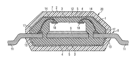
- FIG. 1 is a diagram of a cross section through a composite involving a thermoplastic and a thermoset
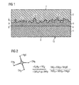
- FIG. 2 shows a system of reactions for flame pyrolysis coating of surfaces with an adhesion-promoter layer which comprises silicates
- FIG. 3 is a diagram of a cross section through a semiconductor component whose casing comprises an adhesion-promoter layer.
- FIG. 1 is a diagram of a cross section of a composite 10 .
- the composite has a first part 1 composed of a thermoset material 3 and has a second part 2 composed of a thermoplastic material 7 .
- the first part 1 has been bonded by way of an adhesion-promoter layer 5 to the second part 2 .
- the adhesion-promoter layer 5 comprises silicates deposited by flame pyrolysis.
- the first part 1 is a thermoset casing of a semiconductor component 20 , which can be seen in FIG. 3 .
- the average thickness D of the adhesion-promoter layer 5 is in the range from 5 to 300 nm, and in the inventive embodiment shown it has a preferred thickness which varies in the range from 5 to 40 nm.
- the lower 5 to 10 nm of the adhesion-promoter layer 5 cover the surface 4 of the thermoset casing 1 of the semi-conductor component 20 , with fully compact morphology.
- the porosity of the adhesion-promoter layer 5 increases, and in the uppermost region it has microporous morphology 6 .
- This microporous morphology 6 of the adhesion-promoter layer 5 increases the level of inter-meshing with the thermoplastic material 7 .
- this microporous morphology 6 of the adhesion-promoter layer 5 provides mechanical anchoring between the thermoset casing material 3 and the thermoplastic material 7 .
- FIG. 2 shows a system of reactions for flame pyrolysis coating of surfaces with an adhesion-promoter layer which comprises silicates.
- an organometallic compound in the form of a tetramethylsilane and derivatives of tetramethylsilane, preferably tetraethylsilane, whose molecular formula is Si(C 2 H 5 ) 4 is introduced into a flame coating system.
- This tetraethylsilane has, as central Me atom, a silicon atom Si, which has four surrounding organic ethyl moieties —C 2 H 5 , as indicated on the left-hand side of FIG. 2 .
- the tetraethylsilane Si(C 2 H 5 ) 4 is, for example, mixed with a propane gas of molecular formula C 3 H 8 and with oxygen 13 O 2 and subjected to combustion, whereupon volatile carbon dioxide 7 CO 2 and water 10 H 2 O are produced as reaction products, and SiO x silicates, preferably silicon dioxide SiO 2 , are deposited on the surface of the parts to be coated, for example of a thermoset or of a thermoplastic.
- FIG. 2 shows another possible reaction, separated by a broken line, in which butane with molecular formula C 4 H 10 is introduced instead of propane with molecular formula C 3 H 8 .
- two tetraethylsilane molecules can react with two butane molecules and twenty-nine O 2 molecules to give SiO x silicate, which is deposited, and volatile carbon dioxide 16 CO 2 , and volatile water 22 H 2 O in the butane flame. It is also possible to use methane with molecular formula CH 4 instead of butane C 4 H 10 for the flame pyrolysis process.
- an SiO x layer is deposited as adhesion-promoter layer on the surfaces of the thermoset casing of a semiconductor component.
- the average layer thickness needed is only from 5 to 40 nm, and up to 300 nm can be deposited if necessary.
- a periodic method for the coating process can be used to reduce the extent of heating of the semiconductor component down to less than 100° C.
- the effective flame-application time is in the region of seconds.
- This type of flame coating process also gives simultaneous surface cleaning and simultaneous surface activation, and the silicates deposited therefore bond intimately to the plastics surface, in this case a thermoset surface.
- Disposal of the reaction products liberated, e.g. amorphous silicon dioxide, and also the volatile water and the volatile carbon dioxide can be achieved very substantially in environmentally compatible fashion, by passing the volatile components into water and collecting or precipitating the excess silicon dioxide.
- FIG. 3 is a diagram of a cross section through a semiconductor component 20 with a semiconductor chip 12 and with a flat conductor frame 8 , which comprises a chip island 9 and flat conductor 13 .
- the reverse side of the semiconductor chip 12 has been mounted on the chip island 9 .
- the contact areas 18 of the semiconductor chip 12 have been connected electrically by way of bonding wires 14 to the contacts 17 of the flat conductors 13 .
- the semiconductor chip 12 , bonding wires 14 , the chip island 9 , and the inner parts of the flat conductors 13 have been embedded in a thermoset material 3 .
- the outer parts 11 of the flat conductors 13 extend out from the thermoset material 3 .
- the outer surface 4 of the thermoset material 3 forms the outer surface of the semiconductor component 20 .
- the outer surfaces 4 of the casing 1 of the semi-conductor component 20 have been coated with an adhesion-promoter layer 5 .
- this semiconductor component 20 all of the surfaces 4 have been provided with a flame-pyrolysis adhesion-promoter layer 5 in order to improve surface adhesion between the surfaces 4 of the casing 1 of the semiconductor component 20 and a thermoplastic material 7 .
- the pyrolytic layer 5 deposited comprises silicates of a reactive compound composed of oxygen and of organometallic molecules, and has porosity 6 and roughness which improves anchoring between the thermoset casing material 3 and the thermoplastic encapsulation material 7 .
- thermoset casing 1 By virtue of the adhesion-promoter layer 5 on the surfaces 4 of the thermoset casing 1 , a marked improvement can be achieved in adhesion between the thermoset 3 and a thermoplastic 7 .
- an organometallic compound or an organosilicon compound is fed into a flame, and the resultant silicate or metal oxide is deposited from the gas phase on the surfaces 4 of the semiconductor components 20 .
- This uniform coating process can take place in a flame tube or by means of passage of the finished mounted semiconductor components 20 through a flame ring, where the residence time in the region of the flame tube or of the flame ring is only a few seconds.
- the outer flat conductors 11 not intended to be provided with an adhesion-promoter layer are protected via application of a protective layer, prior to a coating process in the flame tube or in the ring burner.
- the semiconductor component 20 coated with the adhesion-promoter layer 5 can, after it has been mounted on a printed circuit board, be dependably embedded into a thermoplastic 7 , in order that the component can be better protected from mechanical loads and from damaging environmental conditions.
- the process of mounting and of embedding in a thermoplastic can be carried out at the customer's premises, in order to create an element for subsequent incorporation.
Abstract
Description
- 1 Semiconductor component casing
- 2 Casing retainer
- 3 Thermoset material
- 4 Surface
- 5 Adhesion-promoter layer
- 6 Porosity
- 7 Thermoplastic material
- 8 Flat conductor frame
- 9 Chip island
- 10 Composite
- 11 Outer flat conductor
- 12 Semiconductor chip
- 13 Flat conductor
- 14 Bonding wire
- 15
- 16
- 17 Contact area
- 18 Chip contact area
- 19
- 20 Semiconductor component
Claims (14)
Applications Claiming Priority (4)
| Application Number | Priority Date | Filing Date | Title |
|---|---|---|---|
| DE102005025083.1 | 2005-05-30 | ||
| DE102005025083A DE102005025083B4 (en) | 2005-05-30 | 2005-05-30 | Thermoplastic thermoset composite and method for bonding a thermoplastic material to a thermoset material |
| DE102005025083 | 2005-05-30 | ||
| PCT/DE2006/000724 WO2006128413A1 (en) | 2005-05-30 | 2006-04-26 | Thermoplastic-thermosetting composite and method for bonding a thermoplastic material to a thermosetting material |
Publications (2)
| Publication Number | Publication Date |
|---|---|
| US20090280314A1 US20090280314A1 (en) | 2009-11-12 |
| US8507080B2 true US8507080B2 (en) | 2013-08-13 |
Family
ID=36838670
Family Applications (1)
| Application Number | Title | Priority Date | Filing Date |
|---|---|---|---|
| US11/915,037 Active 2028-06-22 US8507080B2 (en) | 2005-05-30 | 2006-04-26 | Thermoplastic-thermosetting composite and method for bonding a thermoplastic material to a thermosetting material |
Country Status (3)
| Country | Link |
|---|---|
| US (1) | US8507080B2 (en) |
| DE (1) | DE102005025083B4 (en) |
| WO (1) | WO2006128413A1 (en) |
Cited By (4)
| Publication number | Priority date | Publication date | Assignee | Title |
|---|---|---|---|---|
| US20140022720A1 (en) * | 2012-05-17 | 2014-01-23 | Peter Davison | Film insert molding for device manufacture |
| US20140210075A1 (en) * | 2013-01-25 | 2014-07-31 | Samsung Electronics Co., Ltd | Methods for processing substrates |
| US9412703B1 (en) * | 2015-02-17 | 2016-08-09 | Powertech Technology Inc. | Chip package structure having a shielded molding compound |
| US20210296190A1 (en) * | 2020-03-18 | 2021-09-23 | Fuji Electric Co., Ltd. | Semiconductor device |
Families Citing this family (18)
| Publication number | Priority date | Publication date | Assignee | Title |
|---|---|---|---|---|
| KR20090075058A (en) * | 2008-01-03 | 2009-07-08 | 삼성전자주식회사 | Contact terminal of semiconductor test apparatus |
| DE102008040466A1 (en) * | 2008-07-16 | 2010-01-21 | Robert Bosch Gmbh | Power electronics unit |
| DE102009027995A1 (en) * | 2009-07-24 | 2011-01-27 | Robert Bosch Gmbh | Device with a semiconductor device and a housing and method for manufacturing the device |
| DE102009054189A1 (en) | 2009-11-20 | 2011-05-26 | Roman Cihar | Novel shock-damped wheels or castors and methods of making same |
| DE202009018248U1 (en) | 2009-11-20 | 2011-08-26 | Roman Cihar Physikalischer Geräte- & Sondermaschinenbau | New, shock-absorbing wheels or castors |
| CN102959652B (en) | 2011-06-27 | 2015-10-14 | 丰田自动车株式会社 | Reactor and manufacture method thereof |
| US8912450B2 (en) * | 2011-06-27 | 2014-12-16 | Infineon Technologies Ag | Method for attaching a metal surface to a carrier, a method for attaching a chip to a chip carrier, a chip-packaging module and a packaging module |
| US9929038B2 (en) * | 2013-03-07 | 2018-03-27 | Analog Devices Global | Insulating structure, a method of forming an insulating structure, and a chip scale isolator including such an insulating structure |
| DE102014212720A1 (en) * | 2013-07-01 | 2015-01-08 | Continental Teves Ag & Co. Ohg | Sensor with sealing coating |
| US9941565B2 (en) | 2015-10-23 | 2018-04-10 | Analog Devices Global | Isolator and method of forming an isolator |
| US10204732B2 (en) | 2015-10-23 | 2019-02-12 | Analog Devices Global | Dielectric stack, an isolator device and method of forming an isolator device |
| DE102017102603A1 (en) | 2016-02-09 | 2017-08-10 | Comprisetec Gmbh | Thermoplastic hybrid construction for one component |
| DE102016122251A1 (en) * | 2016-11-18 | 2018-05-24 | Infineon Technologies Austria Ag | Method of forming semiconductor devices and semiconductor device |
| JP6441295B2 (en) | 2016-12-26 | 2018-12-19 | 本田技研工業株式会社 | Junction structure and manufacturing method thereof |
| US11642860B2 (en) | 2017-02-13 | 2023-05-09 | The Boeing Company | Method of making thermoplastic composite structures and prepreg tape used therein |
| US11034068B2 (en) * | 2018-04-30 | 2021-06-15 | Raytheon Company | Encapsulating electronics in high-performance thermoplastics |
| KR20230169412A (en) * | 2019-01-02 | 2023-12-15 | 노벨리스 인크. | Systems and methods for laminating can end stock |
| CN112797666B (en) * | 2021-02-04 | 2022-03-01 | 宁波瑞凌新能源科技有限公司 | Radiation refrigeration film and product thereof |
Citations (25)
| Publication number | Priority date | Publication date | Assignee | Title |
|---|---|---|---|---|
| US4359493A (en) | 1977-09-23 | 1982-11-16 | Ppg Industries, Inc. | Method of vapor deposition |
| US4906493A (en) | 1985-04-26 | 1990-03-06 | Sri International | Method of preparing coatings of metal carbides and the like |
| US5096526A (en) * | 1989-11-30 | 1992-03-17 | The Boeing Company | Core bonding and forming of thermoplastic laminates |
| US5153986A (en) | 1991-07-17 | 1992-10-13 | International Business Machines | Method for fabricating metal core layers for a multi-layer circuit board |
| US5730922A (en) * | 1990-12-10 | 1998-03-24 | The Dow Chemical Company | Resin transfer molding process for composites |
| US5753322A (en) * | 1995-04-21 | 1998-05-19 | Ykk Corporation | Antibacterial, antifungal aluminum building materials and fixtures using the materials |
| US5895723A (en) | 1993-08-26 | 1999-04-20 | Fraunhofer-Gesellschaft Zur Foerderung Der Angewandten Forschung E.V. | Composite films |
| US5946556A (en) * | 1998-01-09 | 1999-08-31 | Nec Corporation | Fabrication method of plastic-packaged semiconductor device |
| DE19911477A1 (en) | 1999-03-15 | 2000-09-21 | Intron Jena Ges Fuer Digitale | Sandwich structure, especially for embossed metallic label, includes an applied plastic backing layer, e.g. of fiber reinforced epoxy resin |
| US6150010A (en) * | 1997-03-04 | 2000-11-21 | Texas Instruments Incorporated | Integrated circuit insulator |
| US6228688B1 (en) * | 1997-02-03 | 2001-05-08 | Kabushiki Kaisha Toshiba | Flip-chip resin-encapsulated semiconductor device |
| WO2001047704A1 (en) | 1999-12-29 | 2001-07-05 | Microcoating Technologies, Inc. | Chemical vapor deposition method and coatings produced therefrom |
| US6259157B1 (en) * | 1998-03-11 | 2001-07-10 | Sanyo Electric Co., Ltd. | Hybrid integrated circuit device, and method of manufacturing thereof |
| US20010014420A1 (en) * | 1996-03-21 | 2001-08-16 | Masataka Takeuchi | Ion conductive laminate and production method and use thereof |
| US6319624B1 (en) * | 1994-12-12 | 2001-11-20 | Yamauchi Corporation | Apparatus for calendering magnetic recording medium |
| US20030013235A1 (en) * | 2000-03-08 | 2003-01-16 | Michael Featherby | Electronic device packaging |
| US6605357B1 (en) * | 1999-07-28 | 2003-08-12 | Denso Corporation | Bonding method and bonding structure of thermoplastic resin material |
| EP1365458A1 (en) | 2002-05-23 | 2003-11-26 | General Electric Company | Barrier layer for an article and method of making said barrier layer by expanding thermal plasma |
| US20040194691A1 (en) * | 2001-07-18 | 2004-10-07 | George Steven M | Method of depositing an inorganic film on an organic polymer |
| US20040216494A1 (en) * | 2000-09-19 | 2004-11-04 | Shinichi Kurotani | Burner for combustion or flame hydrolysis, and combustion furnace and process |
| US20040247948A1 (en) | 2001-08-07 | 2004-12-09 | Stephen Behle | Composite material made from a substrate material and a barrier layer material |
| US20050051763A1 (en) * | 2003-09-05 | 2005-03-10 | Helicon Research, L.L.C. | Nanophase multilayer barrier and process |
| US7013965B2 (en) * | 2003-04-29 | 2006-03-21 | General Electric Company | Organic matrices containing nanomaterials to enhance bulk thermal conductivity |
| WO2006034682A1 (en) | 2004-09-28 | 2006-04-06 | Infineon Technologies Ag | Semiconductor component comprising semiconductor component parts that are potted in a plastic housing mass |
| US20070205518A1 (en) | 2004-09-30 | 2007-09-06 | Infineon Technologies Ag | Layer Between Interfaces of Different Components in Semiconductor Devices |
Family Cites Families (1)
| Publication number | Priority date | Publication date | Assignee | Title |
|---|---|---|---|---|
| DD290225A5 (en) * | 1989-11-10 | 1991-05-23 | Seifert,Horst,De | METHOD FOR PREAMBING METAL SURFACES FOR METAL-NON-METAL COMPOUNDS |
-
2005
- 2005-05-30 DE DE102005025083A patent/DE102005025083B4/en not_active Expired - Fee Related
-
2006
- 2006-04-26 WO PCT/DE2006/000724 patent/WO2006128413A1/en active Application Filing
- 2006-04-26 US US11/915,037 patent/US8507080B2/en active Active
Patent Citations (25)
| Publication number | Priority date | Publication date | Assignee | Title |
|---|---|---|---|---|
| US4359493A (en) | 1977-09-23 | 1982-11-16 | Ppg Industries, Inc. | Method of vapor deposition |
| US4906493A (en) | 1985-04-26 | 1990-03-06 | Sri International | Method of preparing coatings of metal carbides and the like |
| US5096526A (en) * | 1989-11-30 | 1992-03-17 | The Boeing Company | Core bonding and forming of thermoplastic laminates |
| US5730922A (en) * | 1990-12-10 | 1998-03-24 | The Dow Chemical Company | Resin transfer molding process for composites |
| US5153986A (en) | 1991-07-17 | 1992-10-13 | International Business Machines | Method for fabricating metal core layers for a multi-layer circuit board |
| US5895723A (en) | 1993-08-26 | 1999-04-20 | Fraunhofer-Gesellschaft Zur Foerderung Der Angewandten Forschung E.V. | Composite films |
| US6319624B1 (en) * | 1994-12-12 | 2001-11-20 | Yamauchi Corporation | Apparatus for calendering magnetic recording medium |
| US5753322A (en) * | 1995-04-21 | 1998-05-19 | Ykk Corporation | Antibacterial, antifungal aluminum building materials and fixtures using the materials |
| US20010014420A1 (en) * | 1996-03-21 | 2001-08-16 | Masataka Takeuchi | Ion conductive laminate and production method and use thereof |
| US6228688B1 (en) * | 1997-02-03 | 2001-05-08 | Kabushiki Kaisha Toshiba | Flip-chip resin-encapsulated semiconductor device |
| US6150010A (en) * | 1997-03-04 | 2000-11-21 | Texas Instruments Incorporated | Integrated circuit insulator |
| US5946556A (en) * | 1998-01-09 | 1999-08-31 | Nec Corporation | Fabrication method of plastic-packaged semiconductor device |
| US6259157B1 (en) * | 1998-03-11 | 2001-07-10 | Sanyo Electric Co., Ltd. | Hybrid integrated circuit device, and method of manufacturing thereof |
| DE19911477A1 (en) | 1999-03-15 | 2000-09-21 | Intron Jena Ges Fuer Digitale | Sandwich structure, especially for embossed metallic label, includes an applied plastic backing layer, e.g. of fiber reinforced epoxy resin |
| US6605357B1 (en) * | 1999-07-28 | 2003-08-12 | Denso Corporation | Bonding method and bonding structure of thermoplastic resin material |
| WO2001047704A1 (en) | 1999-12-29 | 2001-07-05 | Microcoating Technologies, Inc. | Chemical vapor deposition method and coatings produced therefrom |
| US20030013235A1 (en) * | 2000-03-08 | 2003-01-16 | Michael Featherby | Electronic device packaging |
| US20040216494A1 (en) * | 2000-09-19 | 2004-11-04 | Shinichi Kurotani | Burner for combustion or flame hydrolysis, and combustion furnace and process |
| US20040194691A1 (en) * | 2001-07-18 | 2004-10-07 | George Steven M | Method of depositing an inorganic film on an organic polymer |
| US20040247948A1 (en) | 2001-08-07 | 2004-12-09 | Stephen Behle | Composite material made from a substrate material and a barrier layer material |
| EP1365458A1 (en) | 2002-05-23 | 2003-11-26 | General Electric Company | Barrier layer for an article and method of making said barrier layer by expanding thermal plasma |
| US7013965B2 (en) * | 2003-04-29 | 2006-03-21 | General Electric Company | Organic matrices containing nanomaterials to enhance bulk thermal conductivity |
| US20050051763A1 (en) * | 2003-09-05 | 2005-03-10 | Helicon Research, L.L.C. | Nanophase multilayer barrier and process |
| WO2006034682A1 (en) | 2004-09-28 | 2006-04-06 | Infineon Technologies Ag | Semiconductor component comprising semiconductor component parts that are potted in a plastic housing mass |
| US20070205518A1 (en) | 2004-09-30 | 2007-09-06 | Infineon Technologies Ag | Layer Between Interfaces of Different Components in Semiconductor Devices |
Non-Patent Citations (4)
| Title |
|---|
| Choy, K.L., ed. "Innovative Processing of Films and Nanocrylstalline Powders", Imperial College Press (2002) pp. 147-164. * |
| Machine Translation of Kessler, WO-2006/034682 (2012). * |
| Oxford English Dictionary definition of "compact", available at http://www.oed.com/view/Entry/37368 (accessed Jan. 8, 2013). * |
| W.A. Bryant, The Fundamentals of Chemical Vapour Deposition, 12 Journal of Materials Science 1285-1306 (1977). * |
Cited By (7)
| Publication number | Priority date | Publication date | Assignee | Title |
|---|---|---|---|---|
| US20140022720A1 (en) * | 2012-05-17 | 2014-01-23 | Peter Davison | Film insert molding for device manufacture |
| US9426914B2 (en) * | 2012-05-17 | 2016-08-23 | Intel Corporation | Film insert molding for device manufacture |
| US20140210075A1 (en) * | 2013-01-25 | 2014-07-31 | Samsung Electronics Co., Ltd | Methods for processing substrates |
| US9023716B2 (en) * | 2013-01-25 | 2015-05-05 | Samsung Electronics Co., Ltd. | Methods for processing substrates |
| US9412703B1 (en) * | 2015-02-17 | 2016-08-09 | Powertech Technology Inc. | Chip package structure having a shielded molding compound |
| US20210296190A1 (en) * | 2020-03-18 | 2021-09-23 | Fuji Electric Co., Ltd. | Semiconductor device |
| US11462450B2 (en) * | 2020-03-18 | 2022-10-04 | Fuji Electric Co., Ltd. | Semiconductor device |
Also Published As
| Publication number | Publication date |
|---|---|
| DE102005025083B4 (en) | 2007-05-24 |
| DE102005025083A1 (en) | 2006-12-07 |
| US20090280314A1 (en) | 2009-11-12 |
| WO2006128413A1 (en) | 2006-12-07 |
Similar Documents
| Publication | Publication Date | Title |
|---|---|---|
| US8507080B2 (en) | Thermoplastic-thermosetting composite and method for bonding a thermoplastic material to a thermosetting material | |
| US7705472B2 (en) | Semiconductor device with semiconductor device components embedded in a plastic housing composition | |
| JP4320259B2 (en) | Self-adhesive addition-crosslinking silicone rubber compound, method for producing the same, method for producing a composite molded member, and use thereof | |
| CA2401702A1 (en) | Electronic device packaging | |
| KR20120123242A (en) | White color reflecting material and process for production thereof | |
| WO2007017404A2 (en) | Arrangement for hermetically sealing components, and method for the production thereof | |
| JP2010141330A (en) | Flexible substrate, and method of manufacturing the same | |
| KR20190008353A (en) | Multilayer structure, manufacturing method thereof, coating liquid, packaging material, protective sheet for electronic device | |
| KR20000017084A (en) | Silicon dioxide containing coating | |
| US7454836B2 (en) | Method for manufacturing inkjet head, and inkjet head | |
| WO2010129123A2 (en) | Vinylhydrogenpolysiloxane adhesive composition | |
| KR20230002139A (en) | Laminate, silicone resin layer-attached support substrate, silicone resin layer-attached resin substrate, and method for producing electronic device | |
| KR102475941B1 (en) | Laminate, silicone resin layer-attached support substrate, silicone resin layer-attached resin substrate, and method for producing electronic device | |
| CN106661727B (en) | Laminate and method for producing same, and gas barrier film and method for producing same | |
| TWI546406B (en) | Flexible composite, production thereof and use thereof | |
| WO2004085145A1 (en) | Stainless-steel foils with inorganic/organic hybrid film coating | |
| JP2018202850A (en) | Laminate, silicone resin layer-attached support base material, silicone resin layer-attached resin substrate, and method for producing electronic device | |
| KR20210000275A (en) | Method for manufacturing electronic device | |
| WO2018235742A1 (en) | Optical component made of resin and method for manufacturing same | |
| TW201634731A (en) | Printhead coating | |
| US11398588B2 (en) | Optoelectronic component and method for producing an optoelectronic component | |
| KR101494883B1 (en) | Gas barrier film and its preparation method | |
| TWI643734B (en) | A metal core printed circuit board with a hybrid resin layer | |
| JP2018202849A (en) | Laminate, silicone resin layer-attached support base material, silicone resin layer-attached resin substrate, and method for producing electronic device | |
| KR101828153B1 (en) | Surface functional composite film and method of fabricating the same |
Legal Events
| Date | Code | Title | Description |
|---|---|---|---|
| AS | Assignment |
Owner name: INFINEON TECHNOLOGIES AG, GERMANY Free format text: ASSIGNMENT OF ASSIGNORS INTEREST;ASSIGNORS:MAHLER, JOACHIM;HAIMERL, ALFRED;SCHOBER, WOLFGANG;AND OTHERS;REEL/FRAME:021204/0646;SIGNING DATES FROM 20071121 TO 20071126 Owner name: INFINEON TECHNOLOGIES AG, GERMANY Free format text: ASSIGNMENT OF ASSIGNORS INTEREST;ASSIGNORS:MAHLER, JOACHIM;HAIMERL, ALFRED;SCHOBER, WOLFGANG;AND OTHERS;SIGNING DATES FROM 20071121 TO 20071126;REEL/FRAME:021204/0646 |
|
| FEPP | Fee payment procedure |
Free format text: PAYOR NUMBER ASSIGNED (ORIGINAL EVENT CODE: ASPN); ENTITY STATUS OF PATENT OWNER: LARGE ENTITY |
|
| STCF | Information on status: patent grant |
Free format text: PATENTED CASE |
|
| FPAY | Fee payment |
Year of fee payment: 4 |
|
| MAFP | Maintenance fee payment |
Free format text: PAYMENT OF MAINTENANCE FEE, 8TH YEAR, LARGE ENTITY (ORIGINAL EVENT CODE: M1552); ENTITY STATUS OF PATENT OWNER: LARGE ENTITY Year of fee payment: 8 |