US8184453B1 - Increased capacity semiconductor package - Google Patents
Increased capacity semiconductor package Download PDFInfo
- Publication number
- US8184453B1 US8184453B1 US12/183,979 US18397908A US8184453B1 US 8184453 B1 US8184453 B1 US 8184453B1 US 18397908 A US18397908 A US 18397908A US 8184453 B1 US8184453 B1 US 8184453B1
- Authority
- US
- United States
- Prior art keywords
- leads
- die pad
- lead frame
- land
- lands
- Prior art date
- Legal status (The legal status is an assumption and is not a legal conclusion. Google has not performed a legal analysis and makes no representation as to the accuracy of the status listed.)
- Active, expires
Links
- 239000004065 semiconductor Substances 0.000 title abstract description 124
- 238000007747 plating Methods 0.000 claims abstract description 123
- 239000008393 encapsulating agent Substances 0.000 abstract description 82
- 238000000034 method Methods 0.000 abstract description 44
- 238000005530 etching Methods 0.000 abstract description 31
- PXHVJJICTQNCMI-UHFFFAOYSA-N Nickel Chemical compound [Ni] PXHVJJICTQNCMI-UHFFFAOYSA-N 0.000 abstract description 25
- 239000010931 gold Substances 0.000 abstract description 14
- 229910052759 nickel Inorganic materials 0.000 abstract description 8
- 229910052737 gold Inorganic materials 0.000 abstract description 7
- ATJFFYVFTNAWJD-UHFFFAOYSA-N Tin Chemical compound [Sn] ATJFFYVFTNAWJD-UHFFFAOYSA-N 0.000 abstract description 6
- 238000007796 conventional method Methods 0.000 abstract description 2
- 239000000463 material Substances 0.000 description 38
- 238000004519 manufacturing process Methods 0.000 description 25
- KDLHZDBZIXYQEI-UHFFFAOYSA-N Palladium Chemical compound [Pd] KDLHZDBZIXYQEI-UHFFFAOYSA-N 0.000 description 13
- 239000000853 adhesive Substances 0.000 description 7
- 230000001070 adhesive effect Effects 0.000 description 7
- PCHJSUWPFVWCPO-UHFFFAOYSA-N gold Chemical compound [Au] PCHJSUWPFVWCPO-UHFFFAOYSA-N 0.000 description 6
- WABPQHHGFIMREM-UHFFFAOYSA-N lead(0) Chemical compound [Pb] WABPQHHGFIMREM-UHFFFAOYSA-N 0.000 description 6
- 239000000758 substrate Substances 0.000 description 6
- 239000003513 alkali Substances 0.000 description 5
- 230000015572 biosynthetic process Effects 0.000 description 5
- 238000005538 encapsulation Methods 0.000 description 5
- RYGMFSIKBFXOCR-UHFFFAOYSA-N Copper Chemical compound [Cu] RYGMFSIKBFXOCR-UHFFFAOYSA-N 0.000 description 4
- XEEYBQQBJWHFJM-UHFFFAOYSA-N Iron Chemical compound [Fe] XEEYBQQBJWHFJM-UHFFFAOYSA-N 0.000 description 4
- BQCADISMDOOEFD-UHFFFAOYSA-N Silver Chemical compound [Ag] BQCADISMDOOEFD-UHFFFAOYSA-N 0.000 description 4
- 229910052802 copper Inorganic materials 0.000 description 4
- 239000010949 copper Substances 0.000 description 4
- 229910052763 palladium Inorganic materials 0.000 description 4
- 229910052709 silver Inorganic materials 0.000 description 4
- 239000004332 silver Substances 0.000 description 4
- 229910000679 solder Inorganic materials 0.000 description 3
- 241000272168 Laridae Species 0.000 description 2
- 229910052742 iron Inorganic materials 0.000 description 2
- 229910052751 metal Inorganic materials 0.000 description 2
- 239000002184 metal Substances 0.000 description 2
- VYZAMTAEIAYCRO-UHFFFAOYSA-N Chromium Chemical compound [Cr] VYZAMTAEIAYCRO-UHFFFAOYSA-N 0.000 description 1
- 229910000881 Cu alloy Inorganic materials 0.000 description 1
- HCHKCACWOHOZIP-UHFFFAOYSA-N Zinc Chemical compound [Zn] HCHKCACWOHOZIP-UHFFFAOYSA-N 0.000 description 1
- 238000003486 chemical etching Methods 0.000 description 1
- 239000011248 coating agent Substances 0.000 description 1
- 238000000576 coating method Methods 0.000 description 1
- 230000009977 dual effect Effects 0.000 description 1
- 229920006332 epoxy adhesive Polymers 0.000 description 1
- BHEPBYXIRTUNPN-UHFFFAOYSA-N hydridophosphorus(.) (triplet) Chemical compound [PH] BHEPBYXIRTUNPN-UHFFFAOYSA-N 0.000 description 1
- 230000010354 integration Effects 0.000 description 1
- 238000010330 laser marking Methods 0.000 description 1
- 239000007788 liquid Substances 0.000 description 1
- 230000002093 peripheral effect Effects 0.000 description 1
- 229910052725 zinc Inorganic materials 0.000 description 1
- 239000011701 zinc Substances 0.000 description 1
Images


Classifications
-
- H—ELECTRICITY
- H01—ELECTRIC ELEMENTS
- H01L—SEMICONDUCTOR DEVICES NOT COVERED BY CLASS H10
- H01L23/00—Details of semiconductor or other solid state devices
- H01L23/48—Arrangements for conducting electric current to or from the solid state body in operation, e.g. leads, terminal arrangements ; Selection of materials therefor
- H01L23/488—Arrangements for conducting electric current to or from the solid state body in operation, e.g. leads, terminal arrangements ; Selection of materials therefor consisting of soldered or bonded constructions
- H01L23/495—Lead-frames or other flat leads
- H01L23/49541—Geometry of the lead-frame
-
- H—ELECTRICITY
- H01—ELECTRIC ELEMENTS
- H01L—SEMICONDUCTOR DEVICES NOT COVERED BY CLASS H10
- H01L21/00—Processes or apparatus adapted for the manufacture or treatment of semiconductor or solid state devices or of parts thereof
- H01L21/02—Manufacture or treatment of semiconductor devices or of parts thereof
- H01L21/04—Manufacture or treatment of semiconductor devices or of parts thereof the devices having at least one potential-jump barrier or surface barrier, e.g. PN junction, depletion layer or carrier concentration layer
- H01L21/48—Manufacture or treatment of parts, e.g. containers, prior to assembly of the devices, using processes not provided for in a single one of the subgroups H01L21/06 - H01L21/326
- H01L21/4814—Conductive parts
- H01L21/4821—Flat leads, e.g. lead frames with or without insulating supports
- H01L21/4828—Etching
-
- H—ELECTRICITY
- H01—ELECTRIC ELEMENTS
- H01L—SEMICONDUCTOR DEVICES NOT COVERED BY CLASS H10
- H01L23/00—Details of semiconductor or other solid state devices
- H01L23/48—Arrangements for conducting electric current to or from the solid state body in operation, e.g. leads, terminal arrangements ; Selection of materials therefor
- H01L23/488—Arrangements for conducting electric current to or from the solid state body in operation, e.g. leads, terminal arrangements ; Selection of materials therefor consisting of soldered or bonded constructions
- H01L23/495—Lead-frames or other flat leads
- H01L23/49541—Geometry of the lead-frame
- H01L23/49548—Cross section geometry
-
- H—ELECTRICITY
- H01—ELECTRIC ELEMENTS
- H01L—SEMICONDUCTOR DEVICES NOT COVERED BY CLASS H10
- H01L23/00—Details of semiconductor or other solid state devices
- H01L23/48—Arrangements for conducting electric current to or from the solid state body in operation, e.g. leads, terminal arrangements ; Selection of materials therefor
- H01L23/488—Arrangements for conducting electric current to or from the solid state body in operation, e.g. leads, terminal arrangements ; Selection of materials therefor consisting of soldered or bonded constructions
- H01L23/495—Lead-frames or other flat leads
- H01L23/49579—Lead-frames or other flat leads characterised by the materials of the lead frames or layers thereon
- H01L23/49582—Metallic layers on lead frames
-
- H—ELECTRICITY
- H01—ELECTRIC ELEMENTS
- H01L—SEMICONDUCTOR DEVICES NOT COVERED BY CLASS H10
- H01L2224/00—Indexing scheme for arrangements for connecting or disconnecting semiconductor or solid-state bodies and methods related thereto as covered by H01L24/00
- H01L2224/01—Means for bonding being attached to, or being formed on, the surface to be connected, e.g. chip-to-package, die-attach, "first-level" interconnects; Manufacturing methods related thereto
- H01L2224/26—Layer connectors, e.g. plate connectors, solder or adhesive layers; Manufacturing methods related thereto
- H01L2224/31—Structure, shape, material or disposition of the layer connectors after the connecting process
- H01L2224/32—Structure, shape, material or disposition of the layer connectors after the connecting process of an individual layer connector
- H01L2224/321—Disposition
- H01L2224/32151—Disposition the layer connector connecting between a semiconductor or solid-state body and an item not being a semiconductor or solid-state body, e.g. chip-to-substrate, chip-to-passive
- H01L2224/32221—Disposition the layer connector connecting between a semiconductor or solid-state body and an item not being a semiconductor or solid-state body, e.g. chip-to-substrate, chip-to-passive the body and the item being stacked
- H01L2224/32245—Disposition the layer connector connecting between a semiconductor or solid-state body and an item not being a semiconductor or solid-state body, e.g. chip-to-substrate, chip-to-passive the body and the item being stacked the item being metallic
-
- H—ELECTRICITY
- H01—ELECTRIC ELEMENTS
- H01L—SEMICONDUCTOR DEVICES NOT COVERED BY CLASS H10
- H01L2224/00—Indexing scheme for arrangements for connecting or disconnecting semiconductor or solid-state bodies and methods related thereto as covered by H01L24/00
- H01L2224/01—Means for bonding being attached to, or being formed on, the surface to be connected, e.g. chip-to-package, die-attach, "first-level" interconnects; Manufacturing methods related thereto
- H01L2224/42—Wire connectors; Manufacturing methods related thereto
- H01L2224/47—Structure, shape, material or disposition of the wire connectors after the connecting process
- H01L2224/48—Structure, shape, material or disposition of the wire connectors after the connecting process of an individual wire connector
- H01L2224/4805—Shape
- H01L2224/4809—Loop shape
- H01L2224/48091—Arched
-
- H—ELECTRICITY
- H01—ELECTRIC ELEMENTS
- H01L—SEMICONDUCTOR DEVICES NOT COVERED BY CLASS H10
- H01L2224/00—Indexing scheme for arrangements for connecting or disconnecting semiconductor or solid-state bodies and methods related thereto as covered by H01L24/00
- H01L2224/01—Means for bonding being attached to, or being formed on, the surface to be connected, e.g. chip-to-package, die-attach, "first-level" interconnects; Manufacturing methods related thereto
- H01L2224/42—Wire connectors; Manufacturing methods related thereto
- H01L2224/47—Structure, shape, material or disposition of the wire connectors after the connecting process
- H01L2224/48—Structure, shape, material or disposition of the wire connectors after the connecting process of an individual wire connector
- H01L2224/481—Disposition
- H01L2224/48151—Connecting between a semiconductor or solid-state body and an item not being a semiconductor or solid-state body, e.g. chip-to-substrate, chip-to-passive
- H01L2224/48221—Connecting between a semiconductor or solid-state body and an item not being a semiconductor or solid-state body, e.g. chip-to-substrate, chip-to-passive the body and the item being stacked
- H01L2224/48245—Connecting between a semiconductor or solid-state body and an item not being a semiconductor or solid-state body, e.g. chip-to-substrate, chip-to-passive the body and the item being stacked the item being metallic
- H01L2224/48247—Connecting between a semiconductor or solid-state body and an item not being a semiconductor or solid-state body, e.g. chip-to-substrate, chip-to-passive the body and the item being stacked the item being metallic connecting the wire to a bond pad of the item
-
- H—ELECTRICITY
- H01—ELECTRIC ELEMENTS
- H01L—SEMICONDUCTOR DEVICES NOT COVERED BY CLASS H10
- H01L2224/00—Indexing scheme for arrangements for connecting or disconnecting semiconductor or solid-state bodies and methods related thereto as covered by H01L24/00
- H01L2224/73—Means for bonding being of different types provided for in two or more of groups H01L2224/10, H01L2224/18, H01L2224/26, H01L2224/34, H01L2224/42, H01L2224/50, H01L2224/63, H01L2224/71
- H01L2224/732—Location after the connecting process
- H01L2224/73251—Location after the connecting process on different surfaces
- H01L2224/73265—Layer and wire connectors
-
- H—ELECTRICITY
- H01—ELECTRIC ELEMENTS
- H01L—SEMICONDUCTOR DEVICES NOT COVERED BY CLASS H10
- H01L2224/00—Indexing scheme for arrangements for connecting or disconnecting semiconductor or solid-state bodies and methods related thereto as covered by H01L24/00
- H01L2224/91—Methods for connecting semiconductor or solid state bodies including different methods provided for in two or more of groups H01L2224/80 - H01L2224/90
- H01L2224/92—Specific sequence of method steps
- H01L2224/922—Connecting different surfaces of the semiconductor or solid-state body with connectors of different types
- H01L2224/9222—Sequential connecting processes
- H01L2224/92242—Sequential connecting processes the first connecting process involving a layer connector
- H01L2224/92247—Sequential connecting processes the first connecting process involving a layer connector the second connecting process involving a wire connector
-
- H—ELECTRICITY
- H01—ELECTRIC ELEMENTS
- H01L—SEMICONDUCTOR DEVICES NOT COVERED BY CLASS H10
- H01L23/00—Details of semiconductor or other solid state devices
- H01L23/28—Encapsulations, e.g. encapsulating layers, coatings, e.g. for protection
- H01L23/31—Encapsulations, e.g. encapsulating layers, coatings, e.g. for protection characterised by the arrangement or shape
- H01L23/3107—Encapsulations, e.g. encapsulating layers, coatings, e.g. for protection characterised by the arrangement or shape the device being completely enclosed
-
- H—ELECTRICITY
- H01—ELECTRIC ELEMENTS
- H01L—SEMICONDUCTOR DEVICES NOT COVERED BY CLASS H10
- H01L24/00—Arrangements for connecting or disconnecting semiconductor or solid-state bodies; Methods or apparatus related thereto
- H01L24/01—Means for bonding being attached to, or being formed on, the surface to be connected, e.g. chip-to-package, die-attach, "first-level" interconnects; Manufacturing methods related thereto
- H01L24/42—Wire connectors; Manufacturing methods related thereto
- H01L24/47—Structure, shape, material or disposition of the wire connectors after the connecting process
- H01L24/48—Structure, shape, material or disposition of the wire connectors after the connecting process of an individual wire connector
-
- H—ELECTRICITY
- H01—ELECTRIC ELEMENTS
- H01L—SEMICONDUCTOR DEVICES NOT COVERED BY CLASS H10
- H01L2924/00—Indexing scheme for arrangements or methods for connecting or disconnecting semiconductor or solid-state bodies as covered by H01L24/00
- H01L2924/0001—Technical content checked by a classifier
- H01L2924/00014—Technical content checked by a classifier the subject-matter covered by the group, the symbol of which is combined with the symbol of this group, being disclosed without further technical details
-
- H—ELECTRICITY
- H01—ELECTRIC ELEMENTS
- H01L—SEMICONDUCTOR DEVICES NOT COVERED BY CLASS H10
- H01L2924/00—Indexing scheme for arrangements or methods for connecting or disconnecting semiconductor or solid-state bodies as covered by H01L24/00
- H01L2924/01—Chemical elements
- H01L2924/01079—Gold [Au]
-
- H—ELECTRICITY
- H01—ELECTRIC ELEMENTS
- H01L—SEMICONDUCTOR DEVICES NOT COVERED BY CLASS H10
- H01L2924/00—Indexing scheme for arrangements or methods for connecting or disconnecting semiconductor or solid-state bodies as covered by H01L24/00
- H01L2924/15—Details of package parts other than the semiconductor or other solid state devices to be connected
- H01L2924/181—Encapsulation
- H01L2924/183—Connection portion, e.g. seal
- H01L2924/18301—Connection portion, e.g. seal being an anchoring portion, i.e. mechanical interlocking between the encapsulation resin and another package part
Definitions
- the invention relates generally to an increased I/O lead frame and a semiconductor device incorporating the same.
- a lead frame for a semiconductor device is fabricated by mechanical stamping or chemical etching of metal strips.
- the lead frame serves to connect a semiconductor die to an external circuit and fix the semiconductor device to an external device, simultaneously.
- the semiconductor devices using the lead frames include a through-hole mounting type dual inline package (DIP), a surface mounting type quad flat package (QFP) having smaller size and higher electrical performance, a small outline package (SOP), in addition to others.
- DIP through-hole mounting type dual inline package
- QFP surface mounting type quad flat package
- SOP small outline package
- leads of the semiconductor device are projected outwardly through a side portion of an encapsulant at a constant length.
- the size of the semiconductor device becomes larger and the number of input/output pins becomes smaller.
- a semiconductor die may need a large number of input/output pins due to high integration and high functionality, it is difficult for the lead frame to satisfy the need of the semiconductor die.
- a ball grid array (BGA) or a pin grid array (PGA) semiconductor device using a laminate circuit substrate, a tape circuit substrate or a film circuit substrate has been developed in the prior art.
- a plurality of solder balls or metal pins of the semiconductor device are area-arrayed not in a side portion of the encapsulant, but rather in a lower portion of the encapsulant (e.g. a lower portion of a circuit substrate).
- a relatively large number of input/output pins can be provided.
- the semiconductor device has high-priced circuit substrate. Additionally, heatproof performance and electrical performance of the semiconductor device are deteriorated, in comparison with a semiconductor device using a lead frame. In other words, a semiconductor die of the semiconductor device using a lead frame is often directly mounted on a die pad made of a copper material. Additionally, electric performance of semiconductor device can be improved due to high heatproof performance. However, it is difficult for the above-described semiconductor device using the circuit substrate to have the structure of the semiconductor device using the lead frame.
- a lead frame and a semiconductor device including the same.
- the lead frame is provided with a die pad, and first, second and third lands sequentially arranged on an outer circumferential edge.
- the lead frame can separate the first and second lands or the die pad and the first land using a plating layer formed on the lead frame as a mask, instead of using a separate mask by etching after the application of the encapsulant.
- a plurality of lands can be formed at low cost, in comparison with a conventional method.
- the first, second and third lands are exposed to the outside through a lower portion of an encapsulant, and can be surface mounted on an external device through the first, second and third lands.
- a plating layer formed on bottom surfaces of the first, second and third lands of the lead frame and a process for separately plating nickel (Ni)/gold (An), or tin (Sn) can be omitted so as to easily surface mount the semiconductor device to the external device.
- FIG. 1A is a top perspective view illustrating a lead frame according to one exemplary embodiment of the present invention
- FIG. 1B is a bottom plan view of the lead frame of FIG. 1A subsequent to the formation of a plating layer thereon;
- FIG. 1C is a top plan view illustrating the lead frame of FIG. 1A prior to the formation of a plating layer thereon;
- FIG. 1D is a top plan view of the lead frame of FIG. 1A subsequent to the formation of a plating layer thereon;
- FIG. 1E is a bottom view illustrating the lead frame of FIG. 1A prior to the formation of a plating layer thereon;
- FIG. 2 is a cross-sectional view taken along a line 2 - 2 of FIG. 1B ;
- FIG. 3A is a top plan view illustrating a lead frame according to another exemplary embodiment of the present invention.
- FIG. 3B is a bottom plan view of the lead frame shown in FIG. 3A ;
- FIG. 3C is a cross-sectional view taken along line 3 C- 3 C of FIG. 3A ;
- FIG. 4A is a top plan view illustrating a lead frame according to another exemplary embodiment of the present invention.
- FIG. 4B is a bottom plan view of the lead frame shown in FIG. 4A ;
- FIG. 4C is a cross-sectional view taken along line 4 C- 4 C of FIG. 4A ;
- FIG. 5A is a top plan view illustrating a lead frame according to another exemplary embodiment of the present invention.
- FIG. 5B is a bottom plan view of the lead frame shown in FIG. 5A ;
- FIG. 5C is a cross-sectional view taken along line 5 C- 5 C of FIG. 5A ;
- FIG. 6A is a top plan view illustrating a semiconductor device according to another exemplary embodiment of the present invention.
- FIG. 6B is a bottom plan view of the semiconductor device shown in FIG. 6A ;
- FIG. 6C is a cross-sectional view taken along line 6 C- 6 C of FIG. 6A ;
- FIG. 7A is a bottom plan view illustrating a semiconductor device according to another exemplary embodiment of the present invention.
- FIG. 7B is a cross-sectional view taken along line 7 B- 7 B of FIG. 7A ;
- FIG. 8A is a top plan view illustrating a semiconductor device according to another exemplary embodiment of the present invention.
- FIG. 8B is a bottom plan view of the semiconductor device shown in FIG. 8A ;
- FIG. 8C is a cross-sectional view taken along line 8 C- 8 C of FIG. 8A ;
- FIG. 9A is a bottom plan view illustrating a semiconductor device according to another exemplary embodiment of the present invention.
- FIG. 9B is a cross-sectional view taken along a line 9 B- 9 B of FIG. 9A ;
- FIG. 10 is a flow chart illustrating an exemplary fabrication method for the semiconductor device shown in FIGS. 6A-6C ;
- FIGS. 11A to 11J are views illustrating an exemplary fabrication method for the semiconductor device shown in FIGS. 6A-6C .
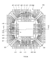
- FIG. 1A depicts a lead frame 100 according to one exemplary embodiment of the present invention.
- the lead frame 100 includes a die pad 110 , a plurality of tie bars 120 formed on the die pad 110 , a frame 130 connecting the tie bars 120 to each other, a plurality of extended leads 140 formed on the frame 130 and a plurality of normal leads 160 formed on the frame 130 .
- the die pad 110 has an approximately quadrangular plate shape with four sides and four corners.
- a semiconductor die is attached to the die pad 110 via an adhesive coating applied to the die pad 110 .
- the die pad 110 is exposed to a lower portion of an encapsulant of the semiconductor device into which the lead frame 100 is integrated. In other words, the die pad 110 is surface-mounted on an external device.
- a plating layer 110 a may be formed on the top and bottom surfaces of the die pad 110 using any one material selected from silver (Ag), a pre-plated frame (PPF) (e.g. a plating layer plated sequentially with nickel (Ni), palladium (Pd) and gold (Au)), solder (Sn) or equivalent materials.
- the plating layer 110 a is hatched in FIGS. 1B and 1D . Additionally, the plating layer 110 a may be formed on a side surface of the die pad 110 .
- Tie bars 120 are projected outwardly from each of the four corners of the die pad 110 at a constant length.
- each tie bar 120 is extended outwardly from a respective corner of the die pad 110 along an imaginary diagonal line.
- a half etching portion 124 is formed on a bottom surface of each tie bar 120 .
- the half etching portion 124 is positioned in an inner side of the encapsulant in the fabricating process for a semiconductor device including the lead frame 100 , and thus the bonding or adhesion force between the die pad 110 and the encapsulant is increased in the semiconductor device.
- a plating layer 120 a may be formed on the top and bottom surfaces of each tie bar 120 .
- the plating layer 120 a may be made of the same material as that of the plating layer 110 a . Thus, the detailed explanation of the material will be omitted.
- the plating layer 120 a is hatched in FIGS. 1B and 1D . Additionally, the plating layer 120 a may be formed on a side surface of
- the frame 130 connects respective ends of the tie bars 120 to each other and fixes the die pad 110 through the tie bars 120 .
- the frame 130 may be formed to extend in spaced, generally parallel relation to respective sides of the die pad 110 . However, the frame 130 is ultimately separated or removed from the tie bars 120 , the extended leads 140 and the normal leads 160 in the fabricating process of the semiconductor device so as to separate or electrically isolate the extended leads 140 from the normal leads 160 .
- a plating layer 130 a may be formed on the top and bottom surfaces of the frame 130 .
- the plating layer 130 a may be made of the same material as that of the layer 110 a . Thus, the detailed explanation of the material will be omitted.
- the plating layer 130 a is hatched in FIGS. 1B and 1D . Additionally, the plating layer 130 a may be formed on a side surface of the frame 130 .
- the extended leads 140 with a predetermined pitch are extended perpendicularly from the frame 130 toward the die pad 110 at a constant length. However, the extended leads 140 do not contact the die pad 110 . Additionally, the extended leads 140 are provided with a first land 145 and a second land 147 , and a half etched portion 143 formed on a top surface between the first and second lands 145 and 147 . The half etched portion 143 is removed to separate the first land 145 electrically from the second land 147 in the fabricating process of the semiconductor device integrating the lead frame 100 . Additionally, the half etched portion 143 is hatched in FIG. 1C .
- Bottom surfaces of the first and second lands 145 and 147 are areas exposed to a lower portion of the encapsulant of the semiconductor device into which the lead frame 100 is integrated.
- the first and second lands 145 and 147 may be surface-mounted to an external device.
- wire bonding area 145 a and 147 a are provided on top surfaces of the extended leads 140 .
- the wire bonding areas 145 a and 147 a are formed on the top surface 145 a of the first land 145 of each of the extended leads 140 and the top surface 147 a of the second land 147 of each of the extended leads 140 , respectively.
- the wire bonding areas 145 a , 147 a though being explained below, are areas for electrically bonding conductive wires.
- a plating layer 140 a is formed on the top and bottom surfaces of the first and second lands 145 and 147 of the extended leads 140 .
- the plating layer 140 a may be made of the same material as that of the plating layer 110 a , and thus the explanation of the material is omitted.
- the plating layer 140 a is hatched in FIGS. 1B and 1D . Additionally, the plating layer 140 a may be formed on a side surface of each of the extended leads 140 and side surfaces of the first and second lands 145 and 147 .
- the normal leads 160 with a predetermined pitch are each extended perpendicularly from the frame 130 toward the die pad 110 at a constant length. However, each of the normal leads 160 has the length shorter than that of the extended leads 140 . In other words, the extended leads 140 and the normal leads 160 are alternately positioned relative to each other, and the length of the extended leads 140 is longer than that of the normal leads 160 .
- Each normal lead 160 is provided with a third land 165 , and a half etched portion 164 is formed on a bottom surface between the third land 165 and the frame 130 .
- a bottom surface of the third land 165 is exposed to a lower portion of the encapsulant of the semiconductor device into which the lead frame 100 is integrated and surface mounted to an external device.
- a wire bonding area 162 is provided on a top surface of each normal lead 160 .
- the wire bonding area 162 is an area electrically bonding conductive wires.
- a plating layer 160 a is formed on the top and bottom surfaces of each of the normal leads 160 .
- the plating layer 160 a may be made of the same material as that of the plating layer 110 a , and the explanation for the material will be omitted.
- the plating layer 160 a is hatched in FIGS. 1B and 1D . Additionally, the plating layer 160 a may be formed on a side surface of each of the normal leads 160 .
- the lead frame 100 as a quad flat no-lead (QFN) package, has high heatproof performance for emitting heat generated from a semiconductor die mounted to the die pad 110 to the outside, and high electrical performance due to a short path for electrically transmitting a signal. Additionally, a downset is not formed on the lead frame 100 and thus a step is not formed therein. As a result, the size and thickness of a semiconductor device including the lead frame 100 can be reduced, in comparison with a conventional lead frame package.
- the lead frame 100 can be fabricated by etching the half etched portion 143 in the fabricating process of the semiconductor device and separating a plurality of first and second lands 145 and 147 electrically from each other. The above-described lead frame 100 can form a plurality of lands at low fabricating cost in comparison with a conventional fabricating method.
- a plating layer 110 a is formed on a bottom surface of the die pad 110 .
- the plating layer 110 a formed on the bottom surface of the die pad 110 is exposed to a lower portion of an encapsulant of a semiconductor device into which the lead frame is integrated.
- the die pad 110 is surface-mounted on an external device through the plating layer 110 a .
- the plating layer 110 a improves the electrical property between the lead frame 100 and the external device when the die pad 110 is surface mounted to the external device.
- the plating layer 110 a may be further formed on the upper and side surfaces of the die pad 110 .
- each extended lead 140 with a predetermined pitch extends outwardly from the die pad 110 , and is provided with the first and second lands 145 and 147 , and the half etch portion 143 between the first and second lands 145 and 147 on the top surface thereof.
- the plating layer 140 a is formed on the top surfaces of the first and second lands 145 and 147 of the extended lead 140 for wire-bonding with a semiconductor die in the fabricating process of the semiconductor device including the lead frame 100 . Additionally, the plating layer 140 a is formed on bottom surfaces of the first and second lands 145 and 147 of each of the extended leads 140 .
- a bottom surface of the plating layer 140 a , formed on the bottom surfaces of the first and second lands 145 and 147 is exposed to a lower portion of the encapsulant of the semiconductor device.
- the plating layer 140 a of the first and second lands 145 and 147 is required to allow for the surface-mounting of the semiconductor device including the lead frame 100 to an external device.
- the plating layer 140 a may be further formed.
- the plating layer 140 a is formed on those areas of each of the extended leads 140 except for the half etched portion 143 thereof. As indicated above, the half etched portion 143 is removed to separate the first land 145 electrically from the second land 147 in the fabricating process of the semiconductor device.
- each normal lead 160 is formed outwardly from the die pad 110 with a predetermined pitch and is provided with the third land 165 , and a half etched portion 164 on a bottom surface between the third land 165 and the frame 130 .
- the plating layer 160 a of each normal lead 160 is formed on a top surface of the third land 165 and a top surface from the third land 165 to the frame 130 for wire-bonding with a semiconductor die in the fabricating process of the semiconductor device including the lead frame 100 .
- the plating layer 160 a is formed on the lower surfaces of the third land 165 and the half etched portion 164 .
- the plating layer 160 a formed on the bottom surface of the third land 165 is exposed to a lower portion of the encapsulant of the semiconductor device. Additionally, a bottom surface of the plating layer 160 a , formed on the third land 165 is used in the surface-mounting of the semiconductor device including the lead frame 100 to an external device.
- the lead frame 200 includes a die pad 110 , a plurality of tie bars 120 formed on the die pad 110 , a frame 130 connecting the tie bars 120 to each other, a plurality of projection leads 240 formed on the die pad 110 , a plurality of second lands 250 formed on the frame 130 and a plurality of normal leads 260 formed on the frame 130 .
- the lead frame 200 has the same structure as that of the lead frame 100 , except for the projection leads 240 , the second lands 250 and normal leads 260 .
- the projection leads 240 with a predetermined pitch are projected outwardly from respective sides of the frame 130 at a constant length.
- the projection leads 240 are extended perpendicularly to the sides of the die pad 110 and outwardly at a constant length.
- each of the projection leads 240 is provided with a first land 245 , and a half etched portion 243 formed on a top surface between the first land 245 and the die pad 110 .
- the half etched portion 243 is removed to separate the first land 245 electrically from the die pad 110 in the fabricating process of the semiconductor device including the lead frame 200 .
- the half etched portion 243 is hatched in FIG. 3A .
- a bottom surface of the first land 245 is exposed to a lower portion of the encapsulant of the semiconductor device including the lead frame 200 and is used in surface mounting a semiconductor device including the lead frame 200 to an external device.
- a plating layer 240 a is formed on the bottom surface of the first land 245 to assist in such surface mounting to the external device.
- a wire bonding area 242 is formed on a top surface of the first land 245 .
- the wire bonding area 242 is an area for electrically bonding conductive wires.
- the plating layer 240 a is formed on a top surface of the projection lead 240 so as to easily perform wire bonding. In other words, the plating layer 240 a is formed on the each projection lead 140 , except for upper, bottom and side surfaces of the half etched portion 243 thereof.
- the plating layer 240 a may be formed on a side surface of the first land 245 of the projection lead 240 .
- the plating layer 240 a may be made of any one material selected from silver (Ag), nickel (Ni)/palladium (Pd)/gold (Au), tin (Sn) or equivalent materials.
- the second land 250 with a predetermined pitch is extended perpendicularly from the frame 130 toward the projection lead 240 formed on the die pad 110 at a constant length.
- the second land 250 and the projection lead 240 are formed on the same straight line or a common axis extending perpendicularly from the die pad 110 to the frame 130 .
- the second land 250 is not in contact with the projection lead 240 of the die pad 110 .
- a bottom surface of the second land 250 is exposed to a lower portion of an encapsulant of the semiconductor device including the lead frame 200 , and is surface mounted to an external device. Additionally, a plating layer 250 a is formed on the bottom surface of the second land 250 for assisting in the surface mounting to the external surface.
- a wire bonding area 252 is formed on a top surface of the second land 250 .
- the wire bonding area 252 is an area for electrically bonding conductive wires.
- a plating layer 250 a may be formed on the top surface of the second land 250 so as to easily perform wire bonding.
- the plating layer 250 a may be formed on a side surface of the second land 250 .
- the plating layer 250 a may be made of the same material as that of the plating layer 240 a . Thus, the detailed explanation of the material will be omitted.
- each normal lead 260 with a predetermined pitch are extended perpendicularly from the frame 130 and toward the die pad 110 at a constant length.
- the length of each normal lead 260 is longer than that of the second land 250 , however, the normal leads 260 do not contact the die pad 110 .
- the second lands 250 and the normal leads 260 are alternately positioned relative to each other and the length of the normal leads 260 is longer than that of the second lands 250 .
- each normal lead 260 is provided with a third land 265 and a half etched portion 264 formed on a bottom surface between the third land 265 and the frame 130 . The half etched portion 264 is hatched in FIG. 3B .
- a bottom surface of the third land 265 is exposed to a lower portion of the encapsulant of the semiconductor device including the lead frame 200 and surface mounted to an external device. Additionally, a plating layer 260 a is formed on the bottom surface of the third land 265 for assisting in the surface mounting to the external device.
- a wire bonding area 262 is formed on the top surface of the normal lead 260 .
- the wired bonding area 262 extends on the top surface from the third land 265 to the frame 130 .
- the wire bonding area 262 is an area for electrically bonding conductive wires, as explained below.
- a plating layer 260 a is formed on the top surface of the normal lead 260 to easily perform wire bonding.
- the plating layer 260 a may be formed on a side surface of the normal lead 260 .
- the plating layer 260 a may be made of the same material as that of the plating layer 240 a . Thus, the detailed explanation of the material will be omitted.
- the lead frame 200 is typically integrated into a quad flat no-lead (QFN) package, and has high heatproof performance for emitting heat generated from the semiconductor die to the outside, and high electrical performance due to a short path for electrically transmitting a signal. Additionally, a downset is not formed in the lead frame 200 and thus a step is not formed therein. As a result, the size and thickness of the package including the lead frame 200 can be reduced, in comparison with a conventional lead frame package.
- the lead frame 200 can be fabricated by etching the half etched portion 243 in addition to the second and third lands 250 and 265 and separating a plurality of first lands 245 electrically from each other in the fabricating process of the semiconductor device including the lead frame 200 .
- the lead frame 200 formed as described above may form a plurality of lands at low cost, in comparison with conventional lead frame fabrication methods.
- a lead frame 300 may include a die pad 310 , a plurality of tie bars 320 formed on the die pad 310 , a dambar 330 connecting the tie bars 320 to each other, a land connection bar 340 spaced from the sides of the die pad 310 and connecting the tie bars 320 to each other, a plurality of first lands 350 formed on the land connection bar 340 , a plurality of extended leads 360 formed on the land connection bar 340 , a plurality of normal leads 370 formed on the dambar 330 and a plurality of external leads 380 formed on the dambar 330 .
- the die pad 310 has an approximately quadrangular plate shape with four sides and four corners.
- a semiconductor die is attached to the die pad 310 after an adhesive is applied to the die pad 310 in a fabrication process for a semiconductor device including the lead frame 300 .
- the die pad 310 is exposed to a lower portion of the encapsulant of the semiconductor device including the lead frame 300 .
- the die pad 310 is surface-mounted on an external device.
- a plating layer 310 a may be formed on the top and bottom surfaces of the die pad 310 from any one material selected from silver (Ag), nickel (Ni)/palladium (Pd)/gold (Au), tin (Sn) or equivalent materials.
- the plating layer 310 a may be formed on the side surfaces of the die pad 310 .
- a half etched portion 314 extends along each of the four sides of the die pad 310 and is recessed relative to the bottom surface thereof.
- the half etched portion 314 is also ultimately covered by the encapsulant of the semiconductor device including the lead frame 300 . As a result, bonding the encapsulant to the die pad 310 can be improved.
- the half etched portion 314 of the die pad 310 is hatched in FIG. 4B .
- the tie bars 320 project or protrude outwardly from respective ones of the four corners of the die pad 310 at a constant length. In other words, each of the tie bars 320 is extended outwardly from a respective corner of the die pad 310 along an imaginary diagonal line. Additionally, a first downset 321 and a second downset 322 are formed in each the tie bar 320 . Accordingly, an outer area of the first downset 321 is positioned higher than the die pad 310 . In other words, only an inner area of the first downset 321 formed on the tie bar 320 extends in generally coplanar relation to the die pad 310 . A plating layer 320 a may be formed on the top and bottom surfaces of each tie bar 320 .
- the plating layer 320 a may be made of the same material as that of the plating layer 310 a . Thus, the detailed explanation of the material will be omitted. Additionally, the plating layer 320 a may be formed on the side surface of each tie bar 320 .
- the dambar 330 connects the tie bars 320 to each other. Accordingly, the dambar 330 has an approximately quadrangular ring shape.
- the dambar 330 may define segments which extend in generally parallel relation to respective sides of the die pad 310 . However, the dambar 330 is removed to separate the extended leads 360 electrically from the normal leads 370 in a fabrication process of a semiconductor device including the lead frame 300 .
- a plating layer 330 a may be further formed on the top and bottom surfaces of the dambar 330 .
- the plating layer 330 a may be made of the same material as that of the plating layer 310 a . Thus, the detailed explanation of the material will be omitted. Additionally, the plating layer 330 a may be formed on the side surface of the dambar 330 .
- the land connection bar 340 is spaced from the four sides and four corners of the die pad 310 , and extends in generally coplanar relation to the die pad 310 . In other words, the land connection bar 340 is spaced from the die pad 310 and formed to extend about the die pad 310 .
- the land connection bar 340 also connects the tie bars 320 to each other.
- a half etched portion 344 is formed on the top surface of the land connection bar 340 . The half etched portion 344 is removed to separate the first lands 350 electrically from the extended leads 360 in the fabrication process of the semiconductor device including the lead frame 300 . Additionally, the half etched portion 344 is hatched in FIG. 4A .
- Support bars 345 are further formed on the land connection bar 340 , each of the support bars 345 connecting the land connection bar 340 and the die pad 310 to each other.
- a plating layer 345 a may be further formed on the top and bottom surfaces of each of the support bars 345 .
- the first lands 350 of predetermined pitch are extended perpendicularly from the land connection bar 340 toward the die pad 310 at a constant length. However, each first land 350 does not contact the die pad 310 . Additionally, a bottom surface of each first land 350 exposed to the lower portion of the encapsulant of the semiconductor device including the lead frame 300 , and defines an area to be surface-mounted to an external device. A plating layer 350 a may formed on the top, bottom and side surfaces of each first land 350 to assist with the surface-mounting to the external device.
- a wire bonding area is defined on the top surface of each first land 350 .
- the wire bonding area 353 is an area for electrically bonding conductive wires, though being explained below.
- the plating layer 350 a may be further formed on the top surface of each first land 350 to easily perform wire bonding.
- the plating layer 350 a may also be formed on a side surface of the first land 350 as also indicated above.
- the plating layer 350 a may be formed by the same material as that of the plating layer 310 a . Thus, the detailed explanation of the material will be omitted.
- the first land 350 is provided with a locking projection 355 formed on both sides or on one side of the first land 350 .
- a half etched portion 355 a is formed on the bottom surface of each locking projection 355 and covered by the encapsulant of the semiconductor device including the lead frame 300 . As a result, bonding force between each first land 350 and the encapsulant can be improved.
- the half etched portion 355 a of each locking projection 355 is hatched in FIG. 4B .
- Each extended lead 360 with a predetermined pitch is extended perpendicularly from the land connection bar 340 toward the dambar 330 at a constant length. Additionally, each extended lead 360 defines a second land 365 . Each second land 365 is adapted for surface mounting to an external device. In FIGS. 4A and 4B , each first land 350 is linerally aligned with a respective one of the second lands 365 .
- Each extended lead 360 is also provided with a first downset 361 and a second downset 362 , which are sequentially formed therein. Accordingly, an outer area of the first downset 361 of each extended lead 360 is positioned higher than the die pad 310 . Additionally, the second land 365 of each extended lead 360 is formed inwardly from the first downset 361 and is connected to the land connection bar 340 .
- Each extended lead 360 defines a wire bonding area 363 on the top surface thereof between the first downset 361 and the second downset 362 .
- the wire bonding area 363 is formed higher than or elevated relative to the die pad 310 .
- the wire bonding area 363 is an area for electrically bonding conductive wires, though being explained below.
- a plating layer 360 a is formed on the top surface of each extended lead 360 to easily perform wire bonding.
- the plating layer 360 a may be formed by the same material as that of the plating layer 310 a . Thus, the detailed explanation of the material will be omitted.
- the plating layer 360 a may also be formed on the bottom and side surfaces of each extended lead 360 .
- a tie bar portion 364 of each extended lead 360 is connected with the dambar 330 .
- the flatness of the land connection bar 340 and the first lands 350 can be maintained.
- the extended tie bar portions 364 are not exposed to the outside of the encapsulant. Accordingly, the extended tie bar portions 364 of the semiconductor device may be electrically coupled to an external device only through the second lands 365 , like the other extended leads 365 .
- Each normal lead 370 with a predetermined pitch is extended perpendicularly from the dambar 330 toward the die pad 310 at a constant length. Additionally, the normal leads 370 and the extended leads 360 are alternately positioned or staggered relative to each other.
- Each normal lead 370 is provided with a downset 371 .
- the downsets 371 of the normal leads 370 correspond to the second downsets 362 .
- each normal lead 370 is provided with a wire bonding area 373 on the top surface thereof between the downset 371 and the die pad 310 .
- the wire bonding area 373 has the same planar shape as that of the wire bonding area 363 of each extended lead 360 .
- the wire bonding area 373 is an area for electrically bonding conductive wires, though being explained below.
- a plating layer 370 a may be formed on the top surface of each normal lead 370 to easily perform wire bonding.
- the plating layer 370 a may be made of the same material as that of the plating layer 310 a . Thus, the detailed explanation of the material will be omitted.
- the plating layer 370 a may also be formed on bottom and side surfaces of each normal lead 370 .
- Each external lead 380 is extended perpendicularly outward from the dambar 330 at a constant length, and is aligned with a respective one of the normal leads 370 .
- the external leads are 380 are electrically coupled to the tie bar 320 , the extended leads 360 and the normal leads 370 .
- the external lead 380 are electrically coupled to only respective ones of the normal lead 370 . Accordingly, an electrical signal through each normal lead 370 is transmitted through the corresponding external lead 380 .
- Each external lead 380 protrudes from a side surface of the encapsulant of the semiconductor device including the lead frame 300 , and is adapted to be surface mounted or through hole mounted on an external device.
- the lead frame 300 formed as described above may separate a plurality of first lands 350 electrically from a plurality of second lands 365 by etching the land connection bar 340 in the fabrication process of the semiconductor device including the lead frame 300 .
- the lead frame 300 formed as described above may form a plurality of lands at low cost, in comparison with conventional lead frame fabrication methods.
- a lead frame 400 may include a die pad 410 , a plurality of tie bars 320 formed on the die pad 410 , a dambar 330 connecting the tie bars 320 to each other, a plurality of projection leads 440 formed on the die pad 410 , a land connection bar 430 extending along and spaced from the sides of the die pad 410 and connecting the tie bars 320 to each other, a plurality of extended leads 460 with a predetermined pitch extending from the land connection bar 430 toward the dambar 330 and each including a second land 465 , a plurality of normal leads 370 formed on the dambar 330 , and a plurality of external leads 380 formed on the dambar 330 .
- the lead frame 400 has the same structure as that of lead frame 300 as described above, except for the die pad 410 and the projection leads 440 . Accordingly, with emphasis on these differences, the die pad 410 has an approximately quadrangular plate shape with four sides and four corners.
- a semiconductor die is attached on the die pad 410 by an adhesive coated on the die pad 410 .
- the die pad 410 is exposed to a lower portion of the encapsulant of the semiconductor device including the lead frame 400 .
- the die pad 410 may be surface mounted on an external device.
- a plating layer 410 a may be formed on the top and bottom surfaces of the die pad 410 from any one material selected from silver (Ag), nickel (Ni)/palladium (Pd)/gold (Au), tin (Sn) or equivalent materials. Additionally, the plating layer 410 a may be formed on a side surface of the die pad 410 .
- each projection lead 440 is provided with a first land 445 , and a half etched portion 443 formed on the top surface between the first land 445 and the die pad 410 .
- the half etched portion 443 is removed to separate the first land 445 electrically from the die pad 410 in the fabrication process of the semiconductor device including the lead frame 400 .
- the half etched portion 443 is hatched in FIG. 5A .
- the bottom surface of the first land 445 is an area exposed to a lower portion of the encapsulant of the semiconductor device including the lead frame 400 , and may be surface mounted to an external device. Additionally, a plating layer 440 a is formed on the bottom surface of the first land 445 for surface mounting with the external device. The plating layer may also be formed on the top and side surfaces of each first land 445 .
- a wire bonding area 442 is provided on the top surface of each first land 445 .
- the wire bonding area 442 is an area for electrically bonding conductive wires, though being explained below.
- the plating layer 440 a may be formed on the top surface of each projection lead 440 to easily perform wire bonding.
- the plating layer 440 a may be made of the same material as that of the plating layer 410 a . Thus, the detailed explanation of the material will be omitted.
- a locking projection 446 may be formed on both sides or one side of each first land 445 .
- a half etched portion 446 a is formed on a bottom surface of each locking projection 446 and covered by the encapsulant of the semiconductor device including the lead frame 400 . As a result, the bonding force of the first land 445 and the encapsulant can be improved.
- the half etched portion 446 a of each locking projection 446 is hatched in FIG. 5B .
- each extended lead 460 is provided with a second land 465 as indicated above.
- Each second land 465 is adapted to be surface mounted to an external device.
- the first land 445 and the second land 465 may be arranged as straight array or a staggered array.
- Each extended lead 460 is also provided with a first downset 461 and a second downset 462 , which are sequentially formed therein. Accordingly, an outer area of the first downset 461 of each extended lead 460 is positioned higher than or elevated relative to the die pad 410 .
- each extended lead 460 is provided with a wire bonding area 463 on a top surface between the first downset 461 and the second downset 462 .
- the wire bonding area 463 is higher than or elevated relative to the die pad 410 .
- the wire bonding area 463 is an area for electrically bonding conductive wires, though being explained below.
- a plating layer 460 a is formed on the top surface of each extended lead 460 to easily perform wire bonding.
- the plating layer 460 a may be made of the same material as that of the plating layer 410 a . Thus, the detailed explanation of the material will be omitted.
- the plating layer 460 a may also be formed on the bottom and side surfaces of each extended lead 460 .
- a half etched portion 444 is formed on a top surface of the land connection bar 430 .
- the half etched portion 444 is removed to separate the extended leads 460 electrically from each other in the fabrication process of the semiconductor device including the lead frame 400 . Additionally, the half etched portion 444 is hatched in FIG. 5A .
- the lead frame 400 according to the present invention can be obtained by etching the half etched portions 443 and 444 in the fabrication process of the semiconductor device including the lead frame 400 to separate the first lands 445 and the second lands 465 electrically from each other.
- the lead frame 400 formed as described above may form a plurality of lands at low cost, in comparison with the existing lead frame fabrication processes.
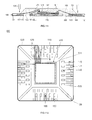
- a semiconductor device 500 includes a lead frame 100 , a semiconductor die 510 , conductive wires 520 and an encapsulant 530 .
- the lead frame 100 includes a die pad 110 , a tie bar (not shown), a plurality of first and second lands 145 and 147 , each corresponding pair of which is defined by an extended lead 140 , and a plurality third land 165 , each of which is defined by a normal lead 160 .
- the lead frame 100 is described in detail above.
- the semiconductor die 510 is attached to the die pad 110 of the lead frame 100 with an adhesive 501 , and a plurality of bond pads 511 are formed on a top surface of the semiconductor die 510 .
- Conductive wires 520 electrically couple the bond pads 511 of the semiconductor die 510 to the first lands 145 of the extended leads 140 , the second lands 147 of the extended leads 140 , and the third lands 165 of the normal leads 160 .
- the encapsulant 530 encapsulates the lead frame 100 , the semiconductor die 510 and the conductive wires 520 so as to protect the lead frame 100 , the semiconductor die 510 and the conductive wires 520 from the external environment.
- the first and second lands 145 and 147 of each extended lead 140 of the lead frame 100 and the third land 165 of each normal lead 160 are exposed to the outside through a lower portion 532 of the encapsulant 530 .
- the die pad 110 is exposed to the outside through the lower portion 532 of the encapsulant 530 .
- a groove 533 is formed by etching a portion between the first and second lands 145 and 147 of each extended lead 140 exposed to the lower portion 532 of the encapsulant 530 .
- the groove 533 electrically separates the first and second lands 145 and 147 .
- the plating layer 140 a is formed on the bottom surfaces of the first and second lands 145 and 147 .
- the plating layer 140 a serves as a mask.
- the etching may be performed alkali etching, but is not limited thereto.
- the etching method may separate the first and second lands 145 and 147 using the plating layer 140 a formed on the lead frame 100 as a mask, without using a separate mask. As a result thereof, a plurality of lands can be formed at low cost in comparison with the conventional lead frame fabrication methods, and thus productivity can be improved.
- each tie bar 120 of the lead frame 100 is positioned within or covered by the encapsulant in the fabrication process of the semiconductor device 500 .
- the bonding force between the die pad 110 and the encapsulant 530 is improved.
- the half etched portion 164 of each normal lead 160 of the lead frame 100 is positioned within or covered by the encapsulant 530 .
- the bonding force of the lead frame 100 and the encapsulant 530 is improved.
- a semiconductor device 600 includes a lead frame 200 , a semiconductor die 510 , conductive wires 520 and an encapsulant 630 .
- the semiconductor device 600 has the same structure as that of the semiconductor device 500 described above, except for the lead frame 200 and the encapsulant 630 . Accordingly, with emphasis on these differences, the lead frame 200 includes the die pad 110 , the tie bars 120 , the first and second lands 245 and 250 defined by the projection leads 240 and the third lands 265 defined by the normal leads 260 .
- the lead frame 200 is described in detail above.
- the encapsulant 630 encapsulates the lead frame 200 , the semiconductor die 510 and the conductive wires 520 so as to protect the lead frame 200 , the semiconductor die 510 and the conductive wires 520 from the external environment.
- the first and second lands 245 and 250 of each projection lead 240 of the lead frame 200 and the third land 265 of each normal lead 260 are exposed to the outside through a lower portion 632 of the encapsulant 630 . Additionally, the die pad 110 is also exposed to the outside through the lower portion 632 of the encapsulant 630 .
- a groove 633 is formed by etching a portion between the die pad 110 exposed to the lower portion 632 of the encapsulant 630 and the first lands 245 of the projection leads 240 .
- the groove 633 electrically separates the die pad 110 and the first lands 245 .
- the plating layers 110 a and 240 a are formed on the bottom surfaces of the die pad 110 and the first lands 245 .
- the plating layers 110 a and 240 a serve as masks. The etching may be performed alkali etching, but is not limited thereto.
- the etching method can separate the die pad 110 and the first lands 245 using the plating layers 110 a and 240 a formed on the lead frame 200 as masks, without using a separate mask.
- the semiconductor device 600 can be fabricated to include the first lands 245 by separating the first lands 245 electrically from the die pad 110 , in addition to the second and third lands 250 and 265 .
- a plurality of lands can be formed at low cost in comparison with conventional lead frame fabrication methods.
- each tie bar 120 of the lead frame 200 is positioned within or covered by the encapsulant 630 in the fabrication process for the semiconductor device 600 .
- the bonding force between the die pad 110 and the encapsulant 630 is increased.
- the half etched portion 264 of each normal lead 260 of the lead frame 200 is positioned within or covered by the encapsulant 630 .
- the bonding force between the lead frame 200 and the encapsulant 630 is increased.
- a semiconductor device 700 includes a lead frame 300 , semiconductor die 710 , conductive wires 720 and an encapsulant 730 .
- the lead frame 300 includes the die pad 310 , the tie bars 320 , the first and second lands 350 and 365 defined by the extended leads 360 , the normal leads 370 and the external leads 380 .
- the lead frame 300 is described in detail above.
- the semiconductor die 710 is attached to the die pad 310 of the lead frame 300 by the adhesive 701 , and a plurality of bond pads 711 are formed on a top surface of the semiconductor die 710 .
- the conductive wires 720 electrically couple the bond pads 711 of the semiconductor die 710 to the first lands 350 , the wire bonding areas 363 of the extended leads 360 , and the wire bonding areas 373 of the normal leads 370 .
- the encapsulant 730 encapsulates the lead frame 300 , the semiconductor die 710 and the conductive wires 720 so as to protect the lead frame 300 , the semiconductor die 710 and the conductive wires 720 from the external environment.
- the external leads 380 of the lead frame 300 are extended from a side portion 731 of the encapsulant 730 and bent to assume a gull wing configuration.
- the first lands 350 of the lead frame 300 and the second lands 365 of the extended leads 360 are exposed to the outside through the lower portion 732 of the encapsulant 730 .
- the die pad 310 and the tie bars 320 connected to the die pad 310 are also exposed to the outside through the lower portion 732 of the encapsulant 730 .
- a groove 733 is formed by etching a portion between the first lands 350 exposed to the lower portion 732 of the encapsulant 730 and the extended leads 360 .
- the groove 733 electrically separates the first lands 350 and the extended leads 360 .
- the plating layers 350 a and 360 a may be formed on the bottom surfaces of the first lands 350 and the extended leads 360 .
- the plating layers 350 a and 360 a serve as masks.
- the etching may be performed by alkali etching, but is not limited thereto.
- the etching method can separate the first lands 350 from the extended leads 360 using the plating layers 350 a and 360 a formed on the lead frame 300 without using a separate mask. As a result, a plurality of lands can be formed at low cost in comparison with the conventional lead frame fabrication methods, and thus productivity can be improved.
- the die pad 310 provided with the half etched portion 314 improves the bonding force between the die pad 310 and the encapsulant 730 since the half etched portion 314 is positioned within or covered by the encapsulant 730 .
- the locking projections 355 of the first lands 350 having the half etched portions 355 a increase the bonding force between the first lands 350 and the encapsulant 730 since they are also covered by the encapsulant.
- a portion of each of the tie bars 320 is positioned within or covered by the encapsulant 730 in the fabrication process of the semiconductor device 700 , thus further improving the bonding force between the die pad 310 and the encapsulant 730 .
- a semiconductor device 800 includes a lead frame 400 , the semiconductor die 710 , the conductive wires 720 and an encapsulant 830 .
- the semiconductor device 800 has the same structure as that of the semiconductor device 700 , except for the lead frame 400 and the encapsulant 830 .
- the lead frame 400 includes a die pad 410 , a tie bar 320 , the first lands 445 of the projection leads 440 , the second lands 465 of the extended leads 460 , the normal leads 370 and the external leads 380 .
- the lead frame 400 is described in detail above.
- the encapsulant 830 encapsulates the lead frame 400 , the semiconductor die 710 and the conductive wires 720 so as to protect the lead frame 400 , the semiconductor die 710 and the conductive wires 720 from the external environment.
- the external leads 380 of the lead frame 400 are extended from a side portion of 831 of the encapsulant 830 at a predetermined length, and are bent to impart a gull wing configuration thereto.
- the first and second lands 445 and 465 of the lead frame 400 are exposed to the outside through a lower portion 832 of the encapsulant 830 . Additionally, the die pad 410 and the tie bars 320 connected to the die pad 410 are also exposed to the outside through the lower portion 832 of the encapsulant 830 .
- a groove 833 is formed by etching a portion between the die pad 410 and the first lands 445 exposed to the lower portion 832 of the encapsulant 830 .
- the groove 833 is formed to electrically separate the die pad 410 and the first lands 445 from each other.
- the plating layers 410 a and 440 a are formed on the bottom surfaces of the die pad 400 and the first lands 445 .
- the plating layers 410 a and 440 a serve as masks.
- the etching may be performed by alkali etching, but is not limited thereto.
- the etching method can separate the die pad 410 from the first lands 445 using the plating layers 410 a and 440 a formed on the lead frame 400 as masks without using a separate mask.
- the semiconductor device 800 can be fabricated to include the first lands 445 in addition to the second lands 465 by separating the first lands 445 electrically from the die pad 410 .
- a plurality of lands can be formed at low cost in comparison with conventional lead frame fabrication methods.
- each first land 445 having the half etched portion is positioned within or covered by the encapsulant 830 .
- the bonding force between the first lands 445 and the encapsulant 830 is improved.
- a portion of each of the tie bars 320 is positioned within or covered by the encapsulant 830 in the process of fabricating the semiconductor device 800 .
- the bonding force between the die pad 410 and the encapsulant 830 is further increased.
- a fabrication method of a semiconductor device includes the steps of preparing a lead frame (S 1 ), attaching a semiconductor die (S 2 ), performing wire bonding (S 3 ), performing encapsulation (S 4 ), performing etching (S 5 ) and cutting a frame (S 6 ).
- a lead frame 100 is prepared including a die pad 110 , a plurality of tie bars (not shown) formed on the die pad 110 , a frame 130 connecting the tie bars to each other, a plurality of extended leads 140 formed on the frame 130 and a plurality of normal leads 160 formed on the frame 130 .
- the structure of the lead frame 100 is explained in detail above. Thus, the detailed explanation will be omitted.
- the semiconductor die 510 on which a plurality of bond pads 511 are formed on the top surface of the semiconductor die 510 is attached to the die pad 110 of the lead frame 100 using an adhesive 501 .
- the adhesive 501 may be made of any one material selected from a common liquid epoxy adhesive, a contacting film, a contacting tape and equivalent materials, but is not limited thereto.
- the semiconductor die 510 is electrically coupled to the lead frame 100 using the conductive wires 520 .
- the bond pads 511 of the semiconductor die 510 are electrically coupled to the first lands 145 of the extended leads 140 , the second lands 147 of the extended leads 140 , and the normal leads 160 .
- the conductive wires 520 is bonded to the wire bonding areas provided on the extended leads 140 and the normal leads 160 .
- the lead frame 100 , the semiconductor die 510 and the conductive wires 520 are encapsulated using the encapsulant 530 .
- the encapsulation is to be performed in an inner area of the frame 130 formed on the lead frame 100 .
- the frame 130 is to be exposed to the outside through the side portion 531 of the encapsulant 530 .
- the encapsulation is performed to expose a lower surface of the die pad 110 of the lead frame 100 , a partial area of the tie bars 120 connected to the die pad 110 , the extended leads 140 , and the third lands 165 provided by the normal leads 160 to the outside.
- the die pad 110 , the partial areas of the tie bars 120 connected to the die pad 110 , the extended lead 140 a and the third land 165 are to be exposed to the outside through the lower portion 532 of the encapsulant 530 .
- a half etched portion provided on the extended leads 140 and exposed to the lower portion 532 of the encapsulant 530 is etched.
- the plating layer 140 a is formed on the bottom surfaces of the first and second lands 145 and 147 of the extended leads 140 being exposed to the lower portion 532 of the encapsulant 530 .
- the plating layer 140 a serves as a mask.
- only the half etched portion is etched.
- the half etched portion is removed by etching and thus a groove 533 is formed in the lower portion 532 of the encapsulant 530 at a constant depth.
- the formation of the groove 533 enables the first and second lands 145 and 147 provided on each extended lead 140 to be electrically independent of each other.
- the method for forming the groove 533 may be performed by alkali etching, but is not limited thereto.
- the etching method may separate the first land 145 from the corresponding second land 147 using the plating layer 140 a formed on the lead frame 100 as a mask, without using a separate mask. As a result thereof, a plurality of lands can be formed at low cost in comparison with conventional lead frame fabrication methods.
- the frame 130 connected to the tie bars 120 , the extended leads 140 and the normal leads 160 is cut and thus the frame 130 and the semiconductor device 500 are separated from each other.
- the tie bars 120 , the extended leads 140 and the normal leads 160 are electrically independent, respectively.
- the frame 130 positioned outside of the encapsulant 530 is cut and separated using a frame cutting tool 535 .
- projection areas of the tie bars 120 , the extended leads 140 and the normal leads 160 which are protrude from the side portion 531 of the encapsulant 530 are removed.
- ink marking or laser marking may be performed on the surface of the encapsulant 530 between the step of performing encapsulation (S 4 ) and the step of cutting the frame (S 5 ). Additionally, the plating layer is formed on the lead frame 100 , and thus a process for plating nickel (Ni)/gold (Au), Ni/Pd/Au, or tin (Sn) on the lands 145 , 147 and 165 exposed to an outer side of the encapsulant 530 will be completed.
Abstract
Description
Claims (20)
Priority Applications (1)
| Application Number | Priority Date | Filing Date | Title |
|---|---|---|---|
| US12/183,979 US8184453B1 (en) | 2008-07-31 | 2008-07-31 | Increased capacity semiconductor package |
Applications Claiming Priority (1)
| Application Number | Priority Date | Filing Date | Title |
|---|---|---|---|
| US12/183,979 US8184453B1 (en) | 2008-07-31 | 2008-07-31 | Increased capacity semiconductor package |
Publications (1)
| Publication Number | Publication Date |
|---|---|
| US8184453B1 true US8184453B1 (en) | 2012-05-22 |
Family
ID=46061285
Family Applications (1)
| Application Number | Title | Priority Date | Filing Date |
|---|---|---|---|
| US12/183,979 Active 2029-12-29 US8184453B1 (en) | 2008-07-31 | 2008-07-31 | Increased capacity semiconductor package |
Country Status (1)
| Country | Link |
|---|---|
| US (1) | US8184453B1 (en) |
Cited By (18)
| Publication number | Priority date | Publication date | Assignee | Title |
|---|---|---|---|---|
| US20110108969A1 (en) * | 2009-11-11 | 2011-05-12 | Byung Tai Do | Integrated circuit packaging system with leads and method of manufacture thereof |
| US20120112330A1 (en) * | 2010-11-10 | 2012-05-10 | Raydium Semiconductor Corporation | Semiconductor device |
| US20120181673A1 (en) * | 2009-08-21 | 2012-07-19 | Stats Chippac, Ltd. | Semiconductor Device and Method of Stacking Die on Leadframe Electrically Connected by Conductive Pillars |
| US8432023B1 (en) * | 2008-10-06 | 2013-04-30 | Amkor Technology, Inc. | Increased I/O leadframe and semiconductor device including same |
| US20130161804A1 (en) * | 2011-12-21 | 2013-06-27 | Clifford R. Fishley | Integrated circuit (ic) leadframe design |
| US8633575B1 (en) * | 2012-05-24 | 2014-01-21 | Amkor Technology, Inc. | IC package with integrated electrostatic discharge protection |
| US20140048920A1 (en) * | 2012-05-02 | 2014-02-20 | Texas Instruments Incorporated | Selective Leadframe Planishing |
| US20140162409A1 (en) * | 2010-03-12 | 2014-06-12 | Siliconware Precision Industries Co., Ltd. | Method for fabricating quad flat non-leaded semiconductor package |
| US8823152B1 (en) * | 2008-10-27 | 2014-09-02 | Amkor Technology, Inc. | Semiconductor device with increased I/O leadframe |
| US9240380B2 (en) | 2009-08-21 | 2016-01-19 | Stats Chippac, Ltd. | Semiconductor device and method of forming interposer frame over semiconductor die to provide vertical interconnect |
| US9275939B1 (en) * | 2011-01-27 | 2016-03-01 | Amkor Technology, Inc. | Semiconductor device including leadframe with a combination of leads and lands and method |
| US9443746B2 (en) | 2014-08-15 | 2016-09-13 | Freescale Semiconductor, Inc. | Floating mold tool for semicondcutor packaging |
| US9632487B2 (en) * | 2015-07-29 | 2017-04-25 | Lg Display Co., Ltd. | Organic light emitting display device |
| US9631481B1 (en) * | 2011-01-27 | 2017-04-25 | Amkor Technology, Inc. | Semiconductor device including leadframe with a combination of leads and lands and method |
| CN107564821A (en) * | 2016-06-30 | 2018-01-09 | 恩智浦美国有限公司 | Encapsulation semiconductor device and forming method with lead frame and inner lead and outside lead |
| USRE48111E1 (en) | 2009-08-21 | 2020-07-21 | JCET Semiconductor (Shaoxing) Co. Ltd. | Semiconductor device and method of forming interposer frame over semiconductor die to provide vertical interconnect |
| US20220115304A1 (en) * | 2020-10-13 | 2022-04-14 | Amkor Technology Singapore Holding Pte. Ltd. | Semiconductor devices and methods of manufacturing semiconductor devices |
| US11450596B2 (en) * | 2019-11-22 | 2022-09-20 | Advanced Semiconductor Engineering, Inc. | Lead frame, package structure and method for manufacturing the same |
Citations (345)
| Publication number | Priority date | Publication date | Assignee | Title |
|---|---|---|---|---|
| US2596993A (en) | 1949-01-13 | 1952-05-20 | United Shoe Machinery Corp | Method and mold for covering of eyelets by plastic injection |
| US3435815A (en) | 1966-07-15 | 1969-04-01 | Micro Tech Mfg Inc | Wafer dicer |
| US3734660A (en) | 1970-01-09 | 1973-05-22 | Tuthill Pump Co | Apparatus for fabricating a bearing device |
| US3838984A (en) | 1973-04-16 | 1974-10-01 | Sperry Rand Corp | Flexible carrier and interconnect for uncased ic chips |
| US4054238A (en) | 1976-03-23 | 1977-10-18 | Western Electric Company, Inc. | Method, apparatus and lead frame for assembling leads with terminals on a substrate |
| US4189342A (en) | 1971-10-07 | 1980-02-19 | U.S. Philips Corporation | Semiconductor device comprising projecting contact layers |
| US4221925A (en) | 1978-09-18 | 1980-09-09 | Western Electric Company, Incorporated | Printed circuit board |
| US4258381A (en) | 1977-12-07 | 1981-03-24 | Steag, Kernergie Gmbh | Lead frame for a semiconductor device suitable for mass production |
| US4289922A (en) | 1979-09-04 | 1981-09-15 | Plessey Incorporated | Integrated circuit package and lead frame |
| US4301464A (en) | 1978-08-02 | 1981-11-17 | Hitachi, Ltd. | Lead frame and semiconductor device employing the same with improved arrangement of supporting leads for securing the semiconductor supporting member |
| US4332537A (en) | 1978-07-17 | 1982-06-01 | Dusan Slepcevic | Encapsulation mold with removable cavity plates |
| US4417266A (en) | 1981-08-14 | 1983-11-22 | Amp Incorporated | Power and ground plane structure for chip carrier |
| US4451224A (en) | 1982-03-25 | 1984-05-29 | General Electric Company | Mold device for making plastic articles from resin |
| US4530152A (en) | 1982-04-01 | 1985-07-23 | Compagnie Industrielle Des Telecommunications Cit-Alcatel | Method for encapsulating semiconductor components using temporary substrates |
| US4541003A (en) | 1978-12-27 | 1985-09-10 | Hitachi, Ltd. | Semiconductor device including an alpha-particle shield |
| US4646710A (en) | 1982-09-22 | 1987-03-03 | Crystal Systems, Inc. | Multi-wafer slicing with a fixed abrasive |
| US4707724A (en) | 1984-06-04 | 1987-11-17 | Hitachi, Ltd. | Semiconductor device and method of manufacturing thereof |
| US4727633A (en) | 1985-08-08 | 1988-03-01 | Tektronix, Inc. | Method of securing metallic members together |
| US4737839A (en) | 1984-03-19 | 1988-04-12 | Trilogy Computer Development Partners, Ltd. | Semiconductor chip mounting system |
| US4756080A (en) | 1986-01-27 | 1988-07-12 | American Microsystems, Inc. | Metal foil semiconductor interconnection method |
| US4812896A (en) | 1986-11-13 | 1989-03-14 | Olin Corporation | Metal electronic package sealed with thermoplastic having a grafted metal deactivator and antioxidant |
| US4862246A (en) | 1984-09-26 | 1989-08-29 | Hitachi, Ltd. | Semiconductor device lead frame with etched through holes |
| US4862245A (en) | 1985-04-18 | 1989-08-29 | International Business Machines Corporation | Package semiconductor chip |
| US4907067A (en) | 1988-05-11 | 1990-03-06 | Texas Instruments Incorporated | Thermally efficient power device package |
| US4920074A (en) | 1987-02-25 | 1990-04-24 | Hitachi, Ltd. | Surface mount plastic package semiconductor integrated circuit, manufacturing method thereof, as well as mounting method and mounted structure thereof |
| US4935803A (en) | 1988-09-09 | 1990-06-19 | Motorola, Inc. | Self-centering electrode for power devices |
| US4942454A (en) | 1987-08-05 | 1990-07-17 | Mitsubishi Denki Kabushiki Kaisha | Resin sealed semiconductor device |
| US4987475A (en) | 1988-02-29 | 1991-01-22 | Digital Equipment Corporation | Alignment of leads for ceramic integrated circuit packages |
| US5018003A (en) | 1988-10-20 | 1991-05-21 | Mitsubishi Denki Kabushiki Kaisha | Lead frame and semiconductor device |
| US5029386A (en) | 1990-09-17 | 1991-07-09 | Hewlett-Packard Company | Hierarchical tape automated bonding method |
| US5041902A (en) | 1989-12-14 | 1991-08-20 | Motorola, Inc. | Molded electronic package with compression structures |
| US5057900A (en) | 1988-10-17 | 1991-10-15 | Semiconductor Energy Laboratory Co., Ltd. | Electronic device and a manufacturing method for the same |
| US5059379A (en) | 1987-07-20 | 1991-10-22 | Mitsubishi Denki Kabushiki Kaisha | Method of resin sealing semiconductor devices |
| US5065223A (en) | 1989-05-31 | 1991-11-12 | Fujitsu Vlsi Limited | Packaged semiconductor device |
| US5070039A (en) | 1989-04-13 | 1991-12-03 | Texas Instruments Incorporated | Method of making an integrated circuit using a pre-served dam bar to reduce mold flash and to facilitate flash removal |
| US5087961A (en) | 1987-01-28 | 1992-02-11 | Lsi Logic Corporation | Semiconductor device package |
| US5091341A (en) | 1989-05-22 | 1992-02-25 | Kabushiki Kaisha Toshiba | Method of sealing semiconductor device with resin by pressing a lead frame to a heat sink using an upper mold pressure member |
| US5096852A (en) | 1988-06-02 | 1992-03-17 | Burr-Brown Corporation | Method of making plastic encapsulated multichip hybrid integrated circuits |
| US5118298A (en) | 1991-04-04 | 1992-06-02 | Advanced Interconnections Corporation | Through hole mounting of integrated circuit adapter leads |
| US5122860A (en) | 1987-08-26 | 1992-06-16 | Matsushita Electric Industrial Co., Ltd. | Integrated circuit device and manufacturing method thereof |
| US5134773A (en) | 1989-05-26 | 1992-08-04 | Gerard Lemaire | Method for making a credit card containing a microprocessor chip |
| US5151039A (en) | 1990-04-06 | 1992-09-29 | Advanced Interconnections Corporation | Integrated circuit adapter having gullwing-shaped leads |
| US5157475A (en) | 1988-07-08 | 1992-10-20 | Oki Electric Industry Co., Ltd. | Semiconductor device having a particular conductive lead structure |
| US5157480A (en) | 1991-02-06 | 1992-10-20 | Motorola, Inc. | Semiconductor device having dual electrical contact sites |
| US5168368A (en) * | 1991-05-09 | 1992-12-01 | International Business Machines Corporation | Lead frame-chip package with improved configuration |
| US5172213A (en) | 1991-05-23 | 1992-12-15 | At&T Bell Laboratories | Molded circuit package having heat dissipating post |
| US5172214A (en) | 1991-02-06 | 1992-12-15 | Motorola, Inc. | Leadless semiconductor device and method for making the same |
| US5175060A (en) | 1989-07-01 | 1992-12-29 | Ibiden Co., Ltd. | Leadframe semiconductor-mounting substrate having a roughened adhesive conductor circuit substrate and method of producing the same |
| US5200809A (en) | 1991-09-27 | 1993-04-06 | Vlsi Technology, Inc. | Exposed die-attach heatsink package |
| US5200362A (en) | 1989-09-06 | 1993-04-06 | Motorola, Inc. | Method of attaching conductive traces to an encapsulated semiconductor die using a removable transfer film |
| US5214845A (en) | 1992-05-11 | 1993-06-01 | Micron Technology, Inc. | Method for producing high speed integrated circuits |
| US5216278A (en) | 1990-12-04 | 1993-06-01 | Motorola, Inc. | Semiconductor device having a pad array carrier package |
| US5218231A (en) | 1989-08-30 | 1993-06-08 | Kabushiki Kaisha Toshiba | Mold-type semiconductor device |
| US5221642A (en) | 1991-08-15 | 1993-06-22 | Staktek Corporation | Lead-on-chip integrated circuit fabrication method |
| US5250841A (en) | 1992-04-06 | 1993-10-05 | Motorola, Inc. | Semiconductor device with test-only leads |
| US5252853A (en) | 1991-09-19 | 1993-10-12 | Mitsubishi Denki Kabushiki Kaisha | Packaged semiconductor device having tab tape and particular power distribution lead structure |
| US5258094A (en) | 1991-09-18 | 1993-11-02 | Nec Corporation | Method for producing multilayer printed wiring boards |
| US5266834A (en) | 1989-03-13 | 1993-11-30 | Hitachi Ltd. | Semiconductor device and an electronic device with the semiconductor devices mounted thereon |
| US5277972A (en) | 1988-09-29 | 1994-01-11 | Tomoegawa Paper Co., Ltd. | Adhesive tapes |
| US5278446A (en) | 1992-07-06 | 1994-01-11 | Motorola, Inc. | Reduced stress plastic package |
| US5279029A (en) | 1990-08-01 | 1994-01-18 | Staktek Corporation | Ultra high density integrated circuit packages method |
| US5281849A (en) | 1991-05-07 | 1994-01-25 | Singh Deo Narendra N | Semiconductor package with segmented lead frame |
| US5285352A (en) | 1992-07-15 | 1994-02-08 | Motorola, Inc. | Pad array semiconductor device with thermal conductor and process for making the same |
| US5294897A (en) | 1992-07-20 | 1994-03-15 | Mitsubishi Denki Kabushiki Kaisha | Microwave IC package |
| US5327008A (en) | 1993-03-22 | 1994-07-05 | Motorola Inc. | Semiconductor device having universal low-stress die support and method for making the same |
| US5332864A (en) | 1991-12-27 | 1994-07-26 | Vlsi Technology, Inc. | Integrated circuit package having an interposer |
| US5335771A (en) | 1990-09-25 | 1994-08-09 | R. H. Murphy Company, Inc. | Spacer trays for stacking storage trays with integrated circuits |
| US5336931A (en) | 1993-09-03 | 1994-08-09 | Motorola, Inc. | Anchoring method for flow formed integrated circuit covers |
| US5343076A (en) | 1990-07-21 | 1994-08-30 | Mitsui Petrochemical Industries, Ltd. | Semiconductor device with an airtight space formed internally within a hollow package |
| US5358905A (en) | 1993-04-02 | 1994-10-25 | Texas Instruments Incorporated | Semiconductor device having die pad locking to substantially reduce package cracking |
| US5365106A (en) | 1992-10-27 | 1994-11-15 | Kabushiki Kaisha Toshiba | Resin mold semiconductor device |
| US5381042A (en) | 1992-03-31 | 1995-01-10 | Amkor Electronics, Inc. | Packaged integrated circuit including heat slug having an exposed surface |
| EP0393997B1 (en) | 1989-04-20 | 1995-02-01 | Honeywell Inc. | Method of providing a variable-pitch leadframe assembly |
| US5391439A (en) | 1990-09-27 | 1995-02-21 | Dai Nippon Printing Co., Ltd. | Leadframe adapted to support semiconductor elements |
| US5406124A (en) | 1992-12-04 | 1995-04-11 | Mitsui Toatsu Chemicals, Inc. | Insulating adhesive tape, and lead frame and semiconductor device employing the tape |
| US5410180A (en) | 1992-07-28 | 1995-04-25 | Shinko Electric Industries Co., Ltd. | Metal plane support for multi-layer lead frames and a process for manufacturing such frames |
| US5414299A (en) | 1993-09-24 | 1995-05-09 | Vlsi Technology, Inc. | Semi-conductor device interconnect package assembly for improved package performance |
| US5417905A (en) | 1989-05-26 | 1995-05-23 | Esec (Far East) Limited | Method of making a card having decorations on both faces |
| US5428248A (en) | 1992-08-21 | 1995-06-27 | Goldstar Electron Co., Ltd. | Resin molded semiconductor package |
| US5435057A (en) | 1990-10-30 | 1995-07-25 | International Business Machines Corporation | Interconnection method and structure for organic circuit boards |
| US5444301A (en) | 1993-06-23 | 1995-08-22 | Goldstar Electron Co. Ltd. | Semiconductor package and method for manufacturing the same |
| US5452511A (en) | 1993-11-04 | 1995-09-26 | Chang; Alexander H. C. | Composite lead frame manufacturing method |
| US5454905A (en) | 1994-08-09 | 1995-10-03 | National Semiconductor Corporation | Method for manufacturing fine pitch lead frame |
| US5467032A (en) | 1993-11-09 | 1995-11-14 | Samsung Electronics Co., Ltd. | Word line driver circuit for a semiconductor memory device |
| US5474958A (en) | 1993-05-04 | 1995-12-12 | Motorola, Inc. | Method for making semiconductor device having no die supporting surface |
| US5484274A (en) | 1992-11-24 | 1996-01-16 | Neu Dynamics Corp. | Encapsulation molding equipment |
| US5493151A (en) | 1993-07-15 | 1996-02-20 | Kabushiki Kaisha Toshiba | Semiconductor device, lead frame and method for manufacturing semiconductor devices |
| US5508556A (en) | 1994-09-02 | 1996-04-16 | Motorola, Inc. | Leaded semiconductor device having accessible power supply pad terminals |
| US5517056A (en) | 1993-09-30 | 1996-05-14 | Motorola, Inc. | Molded carrier ring leadframe having a particular resin injecting area design for gate removal and semiconductor device employing the same |
| US5521429A (en) | 1993-11-25 | 1996-05-28 | Sanyo Electric Co., Ltd. | Surface-mount flat package semiconductor device |
| US5528076A (en) | 1995-02-01 | 1996-06-18 | Motorola, Inc. | Leadframe having metal impregnated silicon carbide mounting area |
| US5534467A (en) | 1993-03-18 | 1996-07-09 | Lsi Logic Corporation | Semiconductor packages for high I/O semiconductor dies |
| US5539251A (en) | 1992-05-11 | 1996-07-23 | Micron Technology, Inc. | Tie bar over chip lead frame design |
| US5543657A (en) | 1994-10-07 | 1996-08-06 | International Business Machines Corporation | Single layer leadframe design with groundplane capability |
| US5544412A (en) | 1994-05-24 | 1996-08-13 | Motorola, Inc. | Method for coupling a power lead to a bond pad in an electronic module |
| US5545923A (en) | 1993-10-22 | 1996-08-13 | Lsi Logic Corporation | Semiconductor device assembly with minimized bond finger connections |
| US5581122A (en) | 1994-10-25 | 1996-12-03 | Industrial Technology Research Institute | Packaging assembly with consolidated common voltage connections for integrated circuits |
| US5592025A (en) | 1992-08-06 | 1997-01-07 | Motorola, Inc. | Pad array semiconductor device |
| US5592019A (en) | 1994-04-19 | 1997-01-07 | Mitsubishi Denki Kabushiki Kaisha | Semiconductor device and module |
| US5594274A (en) | 1993-07-01 | 1997-01-14 | Nec Corporation | Lead frame for use in a semiconductor device and method of manufacturing the semiconductor device using the same |
| US5595934A (en) | 1995-05-17 | 1997-01-21 | Samsung Electronics Co., Ltd. | Method for forming oxide protective film on bonding pads of semiconductor chips by UV/O3 treatment |
| US5604376A (en) | 1994-06-30 | 1997-02-18 | Digital Equipment Corporation | Paddleless molded plastic semiconductor chip package |
| US5608267A (en) | 1992-09-17 | 1997-03-04 | Olin Corporation | Molded plastic semiconductor package including heat spreader |
| US5608265A (en) | 1993-03-17 | 1997-03-04 | Hitachi, Ltd. | Encapsulated semiconductor device package having holes for electrically conductive material |
| US5625222A (en) | 1993-11-18 | 1997-04-29 | Fujitsu Limited | Semiconductor device in a resin package housed in a frame having high thermal conductivity |
| US5633528A (en) | 1994-05-25 | 1997-05-27 | Texas Instruments Incorporated | Lead frame structure for IC devices with strengthened encapsulation adhesion |
| US5637922A (en) | 1994-02-07 | 1997-06-10 | General Electric Company | Wireless radio frequency power semiconductor devices using high density interconnect |
| US5640047A (en) | 1995-09-25 | 1997-06-17 | Mitsui High-Tec, Inc. | Ball grid assembly type semiconductor device having a heat diffusion function and an electric and magnetic shielding function |
| US5639990A (en) | 1992-06-05 | 1997-06-17 | Mitsui Toatsu Chemicals, Inc. | Solid printed substrate and electronic circuit package using the same |
| US5641997A (en) | 1993-09-14 | 1997-06-24 | Kabushiki Kaisha Toshiba | Plastic-encapsulated semiconductor device |
| US5643433A (en) | 1992-12-23 | 1997-07-01 | Shinko Electric Industries Co., Ltd. | Lead frame and method for manufacturing same |
| US5644169A (en) | 1993-03-04 | 1997-07-01 | Goldstar Electron Co., Ltd. | Mold and method for manufacturing a package for a semiconductor chip and the package manufactured thereby |
| US5646831A (en) | 1995-12-28 | 1997-07-08 | Vlsi Technology, Inc. | Electrically enhanced power quad flat pack arrangement |
| US5650663A (en) | 1995-07-03 | 1997-07-22 | Olin Corporation | Electronic package with improved thermal properties |
| US5661088A (en) | 1996-01-11 | 1997-08-26 | Motorola, Inc. | Electronic component and method of packaging |
| US5665996A (en) | 1994-12-30 | 1997-09-09 | Siliconix Incorporated | Vertical power mosfet having thick metal layer to reduce distributed resistance |
| EP0794572A2 (en) | 1996-03-07 | 1997-09-10 | Matsushita Electronics Corporation | Electronic component, method for making the same, and lead frame and mold assembly for use therein |
| US5673479A (en) | 1993-12-20 | 1997-10-07 | Lsi Logic Corporation | Method for mounting a microelectronic circuit peripherally-leaded package including integral support member with spacer |
| US5683806A (en) | 1988-09-29 | 1997-11-04 | Tomoegawa Paper Co., Ltd. | Adhesive tapes |
| US5683943A (en) | 1994-06-14 | 1997-11-04 | Dai Nippon Printing Co., Ltd. | Process for etching a semiconductor lead frame |
| US5689135A (en) | 1995-12-19 | 1997-11-18 | Micron Technology, Inc. | Multi-chip device and method of fabrication employing leads over and under processes |
| US5696666A (en) | 1995-10-11 | 1997-12-09 | Motorola, Inc. | Low profile exposed die chip carrier package |
| US5701034A (en) | 1994-05-03 | 1997-12-23 | Amkor Electronics, Inc. | Packaged semiconductor die including heat sink with locking feature |
| US5703407A (en) | 1995-02-14 | 1997-12-30 | Kabushiki Kaisha Toshiba | Resin-sealed type semiconductor device |
| US5710064A (en) | 1994-08-16 | 1998-01-20 | Samsung Electronics Co., Ltd. | Method for manufacturing a semiconductor package |
| US5723899A (en) | 1994-08-30 | 1998-03-03 | Amkor Electronics, Inc. | Semiconductor lead frame having connection bar and guide rings |
| US5724233A (en) | 1993-07-09 | 1998-03-03 | Fujitsu Limited | Semiconductor device having first and second semiconductor chips with a gap therebetween, a die stage in the gap and associated lead frames disposed in a package, the lead frames providing electrical connections from the chips to an exterior of the packag |
| US5726493A (en) | 1994-06-13 | 1998-03-10 | Fujitsu Limited | Semiconductor device and semiconductor device unit having ball-grid-array type package structure |
| US5736432A (en) | 1996-09-20 | 1998-04-07 | National Semiconductor Corporation | Lead frame with lead finger locking feature and method for making same |
| US5745984A (en) | 1995-07-10 | 1998-05-05 | Martin Marietta Corporation | Method for making an electronic module |
| US5753977A (en) | 1996-03-22 | 1998-05-19 | Mitsubishi Denki Kabushiki Kaisha | Semiconductor device and lead frame therefor |
| US5753532A (en) | 1995-08-30 | 1998-05-19 | Samsung Electronics Co., Ltd. | Method of manufacturing semiconductor chip package |
| EP0844665A2 (en) | 1996-11-21 | 1998-05-27 | Texas Instruments Incorporated | Wafer level packaging |
| US5767566A (en) | 1995-10-18 | 1998-06-16 | Kabushiki Kaisha Toshiba | Plastic mold type semiconductor device |
| US5766972A (en) | 1994-06-02 | 1998-06-16 | Mitsubishi Denki Kabushiki Kaisha | Method of making resin encapsulated semiconductor device with bump electrodes |
| US5770888A (en) | 1995-12-29 | 1998-06-23 | Lg Semicon Co., Ltd. | Integrated chip package with reduced dimensions and leads exposed from the top and bottom of the package |
| US5776798A (en) | 1996-09-04 | 1998-07-07 | Motorola, Inc. | Semiconductor package and method thereof |
| DE19734794A1 (en) | 1997-01-09 | 1998-07-16 | Mitsubishi Electric Corp | Wiring part and lead frame with the wiring part |
| US5783861A (en) | 1994-03-29 | 1998-07-21 | Lg Semicon Co., Ltd. | Semiconductor package and lead frame |
| US5801440A (en) | 1995-10-10 | 1998-09-01 | Acc Microelectronics Corporation | Chip package board having utility rings |
| US5814884A (en) | 1996-10-24 | 1998-09-29 | International Rectifier Corporation | Commonly housed diverse semiconductor die |
| US5814881A (en) | 1996-12-20 | 1998-09-29 | Lsi Logic Corporation | Stacked integrated chip package and method of making same |
| US5814883A (en) | 1995-10-04 | 1998-09-29 | Mitsubishi Denki Kabushiki Kaisha | Packaged semiconductor chip |
| US5817540A (en) | 1996-09-20 | 1998-10-06 | Micron Technology, Inc. | Method of fabricating flip-chip on leads devices and resulting assemblies |
| US5818105A (en) | 1994-07-22 | 1998-10-06 | Nec Corporation | Semiconductor device with plastic material covering a semiconductor chip mounted on a substrate of the device |
| US5821457A (en) | 1994-03-11 | 1998-10-13 | The Panda Project | Semiconductor die carrier having a dielectric epoxy between adjacent leads |
| US5821615A (en) | 1995-12-06 | 1998-10-13 | Lg Semicon Co., Ltd. | Semiconductor chip package having clip-type outlead and fabrication method of same |
| US5835988A (en) | 1996-03-27 | 1998-11-10 | Mitsubishi Denki Kabushiki Kaisha | Packed semiconductor device with wrap around external leads |
| US5834830A (en) | 1995-12-18 | 1998-11-10 | Lg Semicon Co., Ltd. | LOC (lead on chip) package and fabricating method thereof |
| US5844306A (en) | 1995-09-28 | 1998-12-01 | Mitsubishi Denki Kabushiki Kaisha | Die pad structure for solder bonding |
| US5854512A (en) | 1996-09-20 | 1998-12-29 | Vlsi Technology, Inc. | High density leaded ball-grid array package |
| US5854511A (en) | 1995-11-17 | 1998-12-29 | Anam Semiconductor, Inc. | Semiconductor package including heat sink with layered conductive plate and non-conductive tape bonding to leads |
| US5856911A (en) | 1996-11-12 | 1999-01-05 | National Semiconductor Corporation | Attachment assembly for integrated circuits |
| US5859471A (en) | 1992-11-17 | 1999-01-12 | Shinko Electric Industries Co., Ltd. | Semiconductor device having tab tape lead frame with reinforced outer leads |
| US5866942A (en) | 1995-04-28 | 1999-02-02 | Nec Corporation | Metal base package for a semiconductor device |
| US5866939A (en) | 1996-01-21 | 1999-02-02 | Anam Semiconductor Inc. | Lead end grid array semiconductor package |
| US5871782A (en) | 1995-12-30 | 1999-02-16 | Lg Semicon Co. Ltd. | Transfer molding apparatus having laminated chase block |
| US5874784A (en) | 1995-10-25 | 1999-02-23 | Sharp Kabushiki Kaisha | Semiconductor device having external connection terminals provided on an interconnection plate and fabrication process therefor |
| US5877043A (en) | 1996-02-01 | 1999-03-02 | International Business Machines Corporation | Electronic package with strain relief means and method of making |
| US5886397A (en) | 1996-09-05 | 1999-03-23 | International Rectifier Corporation | Crushable bead on lead finger side surface to improve moldability |
| KR100220154B1 (en) | 1996-04-01 | 1999-09-01 | 김규현 | Method manufacture of semiconductor package |
| US5973935A (en) | 1997-04-07 | 1999-10-26 | Micron Technology, Inc. | Interdigitated leads-over-chip lead frame for supporting an integrated circuit die |
| US5977630A (en) | 1997-08-15 | 1999-11-02 | International Rectifier Corp. | Plural semiconductor die housed in common package with split heat sink |
| US6008532A (en) * | 1997-10-23 | 1999-12-28 | Lsi Logic Corporation | Integrated circuit package having bond fingers with alternate bonding areas |
| JP2000150765A (en) | 1998-10-21 | 2000-05-30 | Amkor Technology Inc | Semiconductor integrated circuit plastic package, ultra- compact lead frame for manufacture thereof, and its manufacture |
| USRE36773E (en) | 1993-10-18 | 2000-07-11 | Motorola, Inc. | Method for plating using nested plating buses and semiconductor device having the same |
| US6107679A (en) | 1997-12-22 | 2000-08-22 | Oki Electric Industry Co., Ltd. | Semiconductor device |
| US6143981A (en) | 1998-06-24 | 2000-11-07 | Amkor Technology, Inc. | Plastic integrated circuit package and method and leadframe for making the package |
| US6157074A (en) | 1997-07-16 | 2000-12-05 | Hyundai Electronics Industries Co., Ltd. | Lead frame adapted for variable sized devices, semiconductor package with such lead frame and method for using same |
| KR20000072714A (en) | 2000-09-21 | 2000-12-05 | 이희영 | Mandibular angle retractor |
| US6166430A (en) | 1998-05-27 | 2000-12-26 | Matsushita Electronics Corporation | Lead frame, method for manufacturing the frame, resin-molded semiconductor device and method for manufacturing the device |
| US6169329B1 (en) | 1996-04-02 | 2001-01-02 | Micron Technology, Inc. | Semiconductor devices having interconnections using standardized bonding locations and methods of designing |
| US6177718B1 (en) | 1998-04-28 | 2001-01-23 | Kabushiki Kaisha Toshiba | Resin-sealed semiconductor device |
| US6181002B1 (en) | 1998-12-22 | 2001-01-30 | Sharp Kabushiki Kaisha | Semiconductor device having a plurality of semiconductor chips |
| US6184573B1 (en) | 1999-05-13 | 2001-02-06 | Siliconware Precision Industries Co., Ltd. | Chip packaging |
| US6184465B1 (en) | 1998-11-12 | 2001-02-06 | Micron Technology, Inc. | Semiconductor package |
| US6194777B1 (en) | 1998-06-27 | 2001-02-27 | Texas Instruments Incorporated | Leadframes with selective palladium plating |
| US6197615B1 (en) | 1997-04-04 | 2001-03-06 | Samsung Electronics Co., Ltd. | Method of producing lead frame having uneven surfaces |
| US6198171B1 (en) | 1999-12-30 | 2001-03-06 | Siliconware Precision Industries Co., Ltd. | Thermally enhanced quad flat non-lead package of semiconductor |
| US6201186B1 (en) | 1998-06-29 | 2001-03-13 | Motorola, Inc. | Electronic component assembly and method of making the same |
| US6201292B1 (en) | 1997-04-02 | 2001-03-13 | Dai Nippon Insatsu Kabushiki Kaisha | Resin-sealed semiconductor device, circuit member used therefor |
| US6204554B1 (en) | 1996-09-05 | 2001-03-20 | International Rectifier Corporation | Surface mount semiconductor package |
| US6208023B1 (en) | 1997-07-31 | 2001-03-27 | Matsushita Electronics Corporation | Lead frame for use with an RF powered semiconductor |
| US6208021B1 (en) | 1996-03-27 | 2001-03-27 | Oki Electric Industry Co., Ltd. | Semiconductor device, manufacturing method thereof and aggregate type semiconductor device |
| US6208020B1 (en) | 1999-02-24 | 2001-03-27 | Matsushita Electronics Corporation | Leadframe for use in manufacturing a resin-molded semiconductor device |
| US6211462B1 (en) | 1998-11-05 | 2001-04-03 | Texas Instruments Incorporated | Low inductance power package for integrated circuits |
| US6218731B1 (en) | 1999-05-21 | 2001-04-17 | Siliconware Precision Industries Co., Ltd. | Tiny ball grid array package |
| US6222259B1 (en) | 1998-09-15 | 2001-04-24 | Hyundai Electronics Industries Co., Ltd. | Stack package and method of fabricating the same |
| US6222258B1 (en) | 1996-11-11 | 2001-04-24 | Fujitsu Limited | Semiconductor device and method for producing a semiconductor device |
| US6225146B1 (en) | 1996-12-24 | 2001-05-01 | Matsushita Electronics Corporation | Lead frame, method of manufacturing lead frame, semiconductor device and method of manufacturing semiconductor device |
| US6229200B1 (en) | 1998-06-10 | 2001-05-08 | Asat Limited | Saw-singulated leadless plastic chip carrier |
| US6229205B1 (en) | 1997-06-30 | 2001-05-08 | Samsung Electronics Co., Ltd. | Semiconductor device package having twice-bent tie bar and small die pad |
| US6239384B1 (en) | 1995-09-18 | 2001-05-29 | Tessera, Inc. | Microelectric lead structures with plural conductors |
| US6239367B1 (en) | 1999-01-29 | 2001-05-29 | United Microelectronics Corp. | Multi-chip chip scale package |
| US6238952B1 (en) | 2000-02-29 | 2001-05-29 | Advanced Semiconductor Engineering, Inc. | Low-pin-count chip package and manufacturing method thereof |
| JP3177060B2 (en) | 1992-04-13 | 2001-06-18 | 株式会社リコー | Reversible thermosensitive recording label and card |
| US6256200B1 (en) | 1999-05-27 | 2001-07-03 | Allen K. Lam | Symmetrical package for semiconductor die |
| US6258629B1 (en) | 1999-08-09 | 2001-07-10 | Amkor Technology, Inc. | Electronic device package and leadframe and method for making the package |
| US6261864B1 (en) | 2000-01-28 | 2001-07-17 | Advanced Semiconductor Engineering, Inc. | Low-pin-count chip package and manufacturing method thereof |
| US20010008305A1 (en) | 1998-06-10 | 2001-07-19 | Asat Ltd. | Leadless plastic chip carrier with etch back pad singulation |
| US20010014538A1 (en) | 1998-06-10 | 2001-08-16 | Asat Ltd. | Leadless plastic chip carrier with etch back pad singulation and die attach pad array |
| EP0459493B1 (en) | 1990-06-01 | 2001-08-16 | Kabushiki Kaisha Toshiba | A semiconductor device comprising a TAB tape and its manufacturing method |
| US6281566B1 (en) | 1996-09-30 | 2001-08-28 | Sgs-Thomson Microelectronics S.R.L. | Plastic package for electronic devices |
| US6282095B1 (en) | 1999-02-02 | 2001-08-28 | Compaq Computer Corporation | Method and system for controlling radio frequency radiation in microelectronic packages using heat dissipation structures |
| US6282094B1 (en) | 1999-04-12 | 2001-08-28 | Siliconware Precision Industries, Co., Ltd. | Ball-grid array integrated circuit package with an embedded type of heat-dissipation structure and method of manufacturing the same |
| US6285075B1 (en) | 1998-11-02 | 2001-09-04 | Asat, Limited | Integrated circuit package with bonding planes on a ceramic ring using an adhesive assembly |
| US6291271B1 (en) | 1999-09-14 | 2001-09-18 | Advanced Semiconductor Engineering, Inc. | Method of making semiconductor chip package |
| US6291273B1 (en) | 1996-12-26 | 2001-09-18 | Hitachi, Ltd. | Plastic molded type semiconductor device and fabrication process thereof |
| US6294100B1 (en) | 1998-06-10 | 2001-09-25 | Asat Ltd | Exposed die leadless plastic chip carrier |
| US6294830B1 (en) | 1996-04-18 | 2001-09-25 | Tessera, Inc. | Microelectronic assembly with conductive terminals having an exposed surface through a dielectric layer |
| US6295977B1 (en) | 1998-11-05 | 2001-10-02 | Wacker Chemie Gmbh | Method and device for simultaneously cutting off a multiplicity of wafers from a workpiece |
| US6297548B1 (en) | 1998-06-30 | 2001-10-02 | Micron Technology, Inc. | Stackable ceramic FBGA for high thermal applications |
| US6303997B1 (en) | 1998-04-08 | 2001-10-16 | Anam Semiconductor, Inc. | Thin, stackable semiconductor packages |
| US6303984B1 (en) | 1997-08-12 | 2001-10-16 | Micron Technology, Inc. | Lead frame including angle iron tie bar |
| US6307272B1 (en) | 1998-05-27 | 2001-10-23 | Hitachi, Ltd. | Semiconductor device and method for manufacturing the same |
| US6306685B1 (en) | 2000-02-01 | 2001-10-23 | Advanced Semiconductor Engineering, Inc. | Method of molding a bump chip carrier and structure made thereby |
| US6309909B1 (en) | 1998-07-02 | 2001-10-30 | Mitsubishi Denki Kabushiki Kaisha | Semiconductor device and method of manufacturing the same |
| US6316838B1 (en) | 1999-10-29 | 2001-11-13 | Fujitsu Limited | Semiconductor device |
| US6316822B1 (en) | 1998-09-16 | 2001-11-13 | Texas Instruments Incorporated | Multichip assembly semiconductor |
| US6323550B1 (en) | 1995-06-06 | 2001-11-27 | Analog Devices, Inc. | Package for sealing an integrated circuit die |
| US6326244B1 (en) | 1998-09-03 | 2001-12-04 | Micron Technology, Inc. | Method of making a cavity ball grid array apparatus |
| US6326243B1 (en) | 1995-08-15 | 2001-12-04 | Kabushiki Kaisha Toshiba | Resin sealed semiconductor device including a die pad uniformly having heat conducting paths and circulating holes for fluid resin |
| US6326678B1 (en) | 1993-09-03 | 2001-12-04 | Asat, Limited | Molded plastic package with heat sink and enhanced electrical performance |
| US6335564B1 (en) | 1998-05-06 | 2002-01-01 | Conexant Systems, Inc. | Single Paddle having a semiconductor device and a passive electronic component |
| US6337510B1 (en) | 2000-11-17 | 2002-01-08 | Walsin Advanced Electronics Ltd | Stackable QFN semiconductor package |
| US6339255B1 (en) | 1998-10-24 | 2002-01-15 | Hyundai Electronics Industries Co., Ltd. | Stacked semiconductor chips in a single semiconductor package |
| US6342730B1 (en) | 2000-01-28 | 2002-01-29 | Advanced Semiconductor Engineering, Inc. | Low-pin-count chip package and manufacturing method thereof |
| US20020011654A1 (en) | 2000-07-25 | 2002-01-31 | Naoto Kimura | Semiconductor device |
| US6348726B1 (en) | 2001-01-18 | 2002-02-19 | National Semiconductor Corporation | Multi row leadless leadframe package |
| US20020024122A1 (en) | 2000-08-25 | 2002-02-28 | Samsung Electronics Co., Ltd. | Lead frame having a side ring pad and semiconductor chip package including the same |
| US20020027297A1 (en) | 2000-09-04 | 2002-03-07 | Chikao Ikenaga | Semiconductor package |
| US6355502B1 (en) | 2000-04-25 | 2002-03-12 | National Science Council | Semiconductor package and method for making the same |
| US6359221B1 (en) | 1997-08-04 | 2002-03-19 | Dai Nippon Insatsu Kabushiki Kaisha | Resin sealed semiconductor device, circuit member for use therein |
| US6362525B1 (en) | 1999-11-09 | 2002-03-26 | Cypress Semiconductor Corp. | Circuit structure including a passive element formed within a grid array substrate and method for making the same |
| US20020038873A1 (en) | 2000-09-29 | 2002-04-04 | Michiaki Hiyoshi | Semiconductor device including intermediate wiring element |
| US6369454B1 (en) | 1998-12-31 | 2002-04-09 | Amkor Technology, Inc. | Semiconductor package and method for fabricating the same |
| US6369447B2 (en) | 1998-04-20 | 2002-04-09 | Mitsubishi Denki Kabushiki Kaisha | Plastic-packaged semiconductor device including a plurality of chips |
| US6373127B1 (en) | 1998-09-29 | 2002-04-16 | Texas Instruments Incorporated | Integrated capacitor on the back of a chip |
| US6377464B1 (en) | 1999-01-29 | 2002-04-23 | Conexant Systems, Inc. | Multiple chip module with integrated RF capabilities |
| US6380048B1 (en) | 2001-08-02 | 2002-04-30 | St Assembly Test Services Pte Ltd | Die paddle enhancement for exposed pad in semiconductor packaging |
| US6384472B1 (en) | 2000-03-24 | 2002-05-07 | Siliconware Precision Industries Co., Ltd | Leadless image sensor package structure and method for making the same |
| US6388336B1 (en) | 1999-09-15 | 2002-05-14 | Texas Instruments Incorporated | Multichip semiconductor assembly |
| US6395578B1 (en) | 1999-05-20 | 2002-05-28 | Amkor Technology, Inc. | Semiconductor package and method for fabricating the same |
| US6400004B1 (en) | 2000-08-17 | 2002-06-04 | Advanced Semiconductor Engineering, Inc. | Leadless semiconductor package |
| JP3289162B2 (en) | 1993-11-12 | 2002-06-04 | 本田技研工業株式会社 | Casting method for casting parts |
| US6399415B1 (en) | 2000-03-20 | 2002-06-04 | National Semiconductor Corporation | Electrical isolation in panels of leadless IC packages |
| US20020072147A1 (en) | 2000-10-24 | 2002-06-13 | Murata Manufacturing Co., Ltd. | High-frequency circuit board unit, high frequency module using the same unit, electronic apparatus using the same module, and manufacturing method for the high-frequency circuit board unit |
| US6410979B2 (en) | 1998-12-21 | 2002-06-25 | Nec Corporation | Ball-grid-array semiconductor device with protruding terminals |
| KR20020049944A (en) | 2000-12-20 | 2002-06-26 | 박종섭 | semiconductor package and method for fabricating the same |
| US6414385B1 (en) | 1999-11-08 | 2002-07-02 | Siliconware Precisionindustries Co., Ltd. | Quad flat non-lead package of semiconductor |
| US6421013B1 (en) | 1999-10-04 | 2002-07-16 | Amerasia International Technology, Inc. | Tamper-resistant wireless article including an antenna |
| US6420779B1 (en) | 1999-09-14 | 2002-07-16 | St Assembly Test Services Ltd. | Leadframe based chip scale package and method of producing the same |
| US6423643B1 (en) | 1999-10-01 | 2002-07-23 | Shinko Electric Industries Co., Ltd | Process of making carrier substrate and semiconductor device |
| US6429508B1 (en) | 2000-08-09 | 2002-08-06 | Kostat Semiconductor Co., Ltd. | Semiconductor package having implantable conductive lands and method for manufacturing the same |
| US20020111009A1 (en) | 2001-02-15 | 2002-08-15 | Megic Corporation | Reliable metal bumps on top of I/O pads after removal of test probe marks |
| US6437429B1 (en) | 2001-05-11 | 2002-08-20 | Walsin Advanced Electronics Ltd | Semiconductor package with metal pads |
| US6444499B1 (en) | 2000-03-30 | 2002-09-03 | Amkor Technology, Inc. | Method for fabricating a snapable multi-package array substrate, snapable multi-package array and snapable packaged electronic components |
| US6448633B1 (en) | 1998-11-20 | 2002-09-10 | Amkor Technology, Inc. | Semiconductor package and method of making using leadframe having lead locks to secure leads to encapsulant |
| US6452279B2 (en) | 2000-07-14 | 2002-09-17 | Mitsubishi Denki Kabushiki Kaisha | Semiconductor device |
| US6459148B1 (en) | 2000-11-13 | 2002-10-01 | Walsin Advanced Electronics Ltd | QFN semiconductor package |
| US20020140068A1 (en) | 2001-03-28 | 2002-10-03 | Ming-Hsun Lee | Leadframe-based semiconductor package for multi-media card |
| US20020140061A1 (en) | 2001-03-27 | 2002-10-03 | Lee Hyung Ju | Lead frame for semiconductor package |
| US20020140081A1 (en) | 2000-12-07 | 2002-10-03 | Young-Huang Chou | Highly integrated multi-layer circuit module having ceramic substrates with embedded passive devices |
| US6464121B2 (en) | 2000-12-21 | 2002-10-15 | Xerox Corporation | Specialized tool adapted for a process for manufacture and interconnection between adjoining printed wiring boards |
| US6465883B2 (en) | 1998-07-08 | 2002-10-15 | Telefonaktiebolaget Lm Ericsson (Publ) | Capsule for at least one high power transistor chip for high frequencies |
| US6472735B2 (en) | 2000-06-21 | 2002-10-29 | Harlan R. Isaak | Three-dimensional memory stacking using anisotropic epoxy interconnections |
| US20020158318A1 (en) | 2001-04-25 | 2002-10-31 | Chen Hung Nan | Multi-chip module |
| US6476474B1 (en) | 2000-10-10 | 2002-11-05 | Siliconware Precision Industries Co., Ltd. | Dual-die package structure and method for fabricating the same |
| US6475646B2 (en) | 2000-08-17 | 2002-11-05 | Samsung Techwin Co., Ltd. | Lead frame and method of manufacturing the lead frame |
| US6476469B2 (en) | 2000-11-23 | 2002-11-05 | Siliconware Precision Industries Co., Ltd. | Quad flat non-leaded package structure for housing CMOS sensor |
| US20020163015A1 (en) | 2001-02-27 | 2002-11-07 | Chippac, Inc. | Plastic semiconductor package |
| US20020167060A1 (en) | 2001-03-02 | 2002-11-14 | Buijsman Adrianus Alphonsus Jozef | Module and electronic device |
| US6482680B1 (en) | 2001-07-20 | 2002-11-19 | Carsem Semiconductor Sdn, Bhd. | Flip-chip on lead frame |
| US6483178B1 (en) | 2000-07-14 | 2002-11-19 | Siliconware Precision Industries Co., Ltd. | Semiconductor device package structure |
| US6492718B2 (en) | 1999-12-20 | 2002-12-10 | Kabushiki Kaisha Toshiba | Stacked semiconductor device and semiconductor system |
| US6495909B2 (en) | 2000-01-05 | 2002-12-17 | Advanced Semiconductor Engineering, Inc. | Low-pin-count chip package and manufacturing method thereof |
| US6498392B2 (en) | 2000-01-24 | 2002-12-24 | Nec Corporation | Semiconductor devices having different package sizes made by using common parts |
| US6498099B1 (en) | 1998-06-10 | 2002-12-24 | Asat Ltd. | Leadless plastic chip carrier with etch back pad singulation |
| US20030006055A1 (en) | 2001-07-05 | 2003-01-09 | Walsin Advanced Electronics Ltd | Semiconductor package for fixed surface mounting |
| US6507120B2 (en) | 2000-12-22 | 2003-01-14 | Siliconware Precision Industries Co., Ltd. | Flip chip type quad flat non-leaded package |
| US6507096B2 (en) | 2000-08-09 | 2003-01-14 | Kostat Semiconductor Co., Ltd. | Tape having implantable conductive lands for semiconductor packaging process and method for manufacturing the same |
| US6518089B2 (en) | 2001-02-02 | 2003-02-11 | Texas Instruments Incorporated | Flip chip semiconductor device in a molded chip scale package (CSP) and method of assembly |
| US20030030131A1 (en) | 2000-09-15 | 2003-02-13 | Samsung Techwin Co., Ltd., | Semiconductor package apparatus and method |
| US6525942B2 (en) | 2000-09-19 | 2003-02-25 | Siliconware Precision Industries Co., Ltd. | Heat dissipation ball grid array package |
| US20030059644A1 (en) | 2001-09-21 | 2003-03-27 | Intel Corporation | Thermo-mechanically robust C4 ball-limiting metallurgy to prevent failure due to die-package interaction and method of making same |
| US6545332B2 (en) | 2001-01-17 | 2003-04-08 | Siliconware Precision Industries Co., Ltd. | Image sensor of a quad flat package |
| US6545345B1 (en) | 2001-03-20 | 2003-04-08 | Amkor Technology, Inc. | Mounting for a package containing a chip |
| US20030073265A1 (en) | 2001-10-12 | 2003-04-17 | Tom Hu | Semiconductor package with singulation crease |
| US6552421B2 (en) | 2000-06-09 | 2003-04-22 | Hitachi, Ltd. | Semiconductor device and a method of manufacturing the same |
| US6559525B2 (en) | 2000-01-13 | 2003-05-06 | Siliconware Precision Industries Co., Ltd. | Semiconductor package having heat sink at the outer surface |
| EP0936671B1 (en) | 1998-02-12 | 2003-05-07 | Hitachi, Ltd. | Resin-moulded semiconductor hybrid module and manufacturing method thereof |
| US6580161B2 (en) | 2001-01-25 | 2003-06-17 | Rohm Co., Ltd. | Semiconductor device and method of making the same |
| US6583503B2 (en) | 1997-03-10 | 2003-06-24 | Micron Technology, Inc. | Semiconductor package with stacked substrates and multiple semiconductor dice |
| US6585905B1 (en) | 1998-06-10 | 2003-07-01 | Asat Ltd. | Leadless plastic chip carrier with partial etch die attach pad |
| US20030164554A1 (en) | 2001-08-06 | 2003-09-04 | Fee Setho Sing | Quad flat no lead (QFN) grid array package, method of making and memory module and computer system including same |
| US20030168719A1 (en) | 2002-03-06 | 2003-09-11 | Cheng Man Hon | Multi-row leadframe |
| US6624005B1 (en) | 2000-09-06 | 2003-09-23 | Amkor Technology, Inc. | Semiconductor memory cards and method of making same |
| US6627977B1 (en) | 2002-05-09 | 2003-09-30 | Amkor Technology, Inc. | Semiconductor package including isolated ring structure |
| US20030198032A1 (en) | 2002-04-23 | 2003-10-23 | Paul Collander | Integrated circuit assembly and method for making same |
| US6646339B1 (en) | 1999-10-15 | 2003-11-11 | Amkor Technology, Inc. | Thin and heat radiant semiconductor package and method for manufacturing |
| US6667546B2 (en) | 2001-11-15 | 2003-12-23 | Siliconware Precision Industries Co., Ltd. | Ball grid array semiconductor package and substrate without power ring or ground ring |
| US6677663B1 (en) | 1999-12-30 | 2004-01-13 | Amkor Technology, Inc. | End grid array semiconductor package |
| US6686649B1 (en) | 2001-05-14 | 2004-02-03 | Amkor Technology, Inc. | Multi-chip semiconductor package with integral shield and antenna |
| US20040027788A1 (en) | 2002-08-08 | 2004-02-12 | Tz-Cheng Chiu | Polymer-embedded solder bumps for reliable plastic package attachment |
| US6696752B2 (en) | 2000-05-22 | 2004-02-24 | Siliconware Precision Industries Co., Ltd. | Encapsulated semiconductor device with flash-proof structure |
| US6700189B2 (en) | 2000-10-10 | 2004-03-02 | Rohm Co., Ltd. | Resin sealed semiconductor device |
| US20040056277A1 (en) | 2002-09-17 | 2004-03-25 | Chippac, Inc. | Semiconductor multi-package module including stacked-die package and having wire bond interconnect between stacked packages |
| US6713375B2 (en) | 1998-12-17 | 2004-03-30 | Koninklijke Philips Electronics N.V. | Method of making an electronic product including package-based inductor coupled to integrated circuit |
| US20040061212A1 (en) | 2002-09-17 | 2004-04-01 | Chippac, Inc. | Semiconductor multi-package module having wire bond interconnect between stacked packages |
| US20040063242A1 (en) | 2002-09-17 | 2004-04-01 | Chippac, Inc. | Semiconductor multi-package module having package stacked over ball grid array package and having wire bond interconnect between stacked packages |
| US20040061213A1 (en) | 2002-09-17 | 2004-04-01 | Chippac, Inc. | Semiconductor multi-package module having package stacked over die-up flip chip ball grid array package and having wire bond interconnect between stacked packages |
| US20040063246A1 (en) | 2002-09-17 | 2004-04-01 | Chippac, Inc. | Semiconductor multi-package module having package stacked over die-down flip chip ball grid array package and having wire bond interconnect between stacked packages |
| US20040065963A1 (en) | 2002-09-17 | 2004-04-08 | Chippac, Inc. | Semiconductor multi-package module having wire bond interconnect between stacked packages and having electrical shield |
| US20040080025A1 (en) | 2002-09-17 | 2004-04-29 | Shinko Electric Industries Co., Ltd. | Lead frame, method of manufacturing the same, and semiconductor device manufactured with the same |
| US20040089926A1 (en) | 2002-11-12 | 2004-05-13 | Taiwan Ic Packaging Corporation | Ultra thin semiconductor device |
| US6757178B2 (en) | 2001-02-23 | 2004-06-29 | Renesas Technology Corp. | Electronic circuit equipment using multilayer circuit board |
| US20040164387A1 (en) | 2003-02-21 | 2004-08-26 | Dai Nippon Printing Co., Ltd. | Semiconductor device fabricating apparatus and semiconductor device fabricating method |
| US6800936B2 (en) | 2001-05-07 | 2004-10-05 | Sony Corporation | High-frequency module device |
| EP0720225B1 (en) | 1994-12-30 | 2004-10-27 | SILICONIX Incorporated | Lateral power MOSFET having metal strap layer to reduce distributed resistance and method of fabricating the same |
| US6812552B2 (en) | 2002-04-29 | 2004-11-02 | Advanced Interconnect Technologies Limited | Partially patterned lead frames and methods of making and using the same in semiconductor packaging |
| US6818973B1 (en) | 2002-09-09 | 2004-11-16 | Amkor Technology, Inc. | Exposed lead QFP package fabricated through the use of a partial saw process |
| US20040253803A1 (en) | 2003-06-16 | 2004-12-16 | Akira Tomono | Packaging assembly and method of assembling the same |
| US6858919B2 (en) | 2000-03-25 | 2005-02-22 | Amkor Technology, Inc. | Semiconductor package |
| US6867492B2 (en) | 2002-01-17 | 2005-03-15 | Infineon Technologies Ag | Radio-frequency power component, radio-frequency power module, method for producing a radio-frequency power component, and method for producing a radio-frequency power module |
| US6897552B2 (en) | 2001-12-12 | 2005-05-24 | Kabushiki Kaisha Toshiba | Semiconductor device wherein chips are stacked to have a fine pitch structure |
| US6927478B2 (en) | 2001-01-15 | 2005-08-09 | Amkor Technology, Inc. | Reduced size semiconductor package with stacked dies |
| US20050199987A1 (en) * | 2002-04-30 | 2005-09-15 | Tadatoshi Danno | Semiconductor device and electronic device |
| US7002805B2 (en) | 2002-12-30 | 2006-02-21 | Advanced Semiconductor Engineering Inc. | Thermal enhance MCM package and manufacturing method thereof |
| US7005327B2 (en) | 2002-09-11 | 2006-02-28 | Advanced Semiconductor Engineering, Inc. | Process and structure for semiconductor package |
| US7009283B1 (en) * | 1999-04-14 | 2006-03-07 | Amkor Technology, Inc. | Nonexposed heat sink for semiconductor package |
| US7015571B2 (en) | 2003-11-12 | 2006-03-21 | Advanced Semiconductor Engineering, Inc. | Multi-chips module assembly package |
| US20060087020A1 (en) | 2004-10-22 | 2006-04-27 | Matsushita Electric Industrial Co., Ltd. | Semiconductor device and method for producing the same |
| US7045396B2 (en) | 1999-12-16 | 2006-05-16 | Amkor Technology, Inc. | Stackable semiconductor package and method for manufacturing same |
| US7053469B2 (en) | 2004-03-30 | 2006-05-30 | Advanced Semiconductor Engineering, Inc. | Leadless semiconductor package and manufacturing method thereof |
| US20060157843A1 (en) | 2005-01-17 | 2006-07-20 | Sung-Wook Hwang | Stacked semiconductor package having interposing print circuit board |
| US7102209B1 (en) | 2003-08-27 | 2006-09-05 | National Semiconductor Corporation | Substrate for use in semiconductor manufacturing and method of making same |
| US20060231939A1 (en) | 2005-04-19 | 2006-10-19 | Takeshi Kawabata | Multilevel semiconductor module and method for fabricating the same |
| US20070023202A1 (en) | 2005-07-29 | 2007-02-01 | Sanyo Electric Co., Ltd. | Circuit board and circuit apparatus using the same |
| US7185426B1 (en) | 2002-05-01 | 2007-03-06 | Amkor Technology, Inc. | Method of manufacturing a semiconductor package |
| US7193298B2 (en) | 2002-02-01 | 2007-03-20 | Infineon Technologies Ag | Lead frame |
| US7245007B1 (en) | 2003-09-18 | 2007-07-17 | Amkor Technology, Inc. | Exposed lead interposer leadframe package |
| US7253503B1 (en) | 1999-11-05 | 2007-08-07 | Amkor Technology, Inc. | Integrated circuit device packages and substrates for making the packages |
| JP4098864B2 (en) | 1997-12-26 | 2008-06-11 | 東北リコー株式会社 | Paper discharge device |
| US7687892B2 (en) * | 2006-08-08 | 2010-03-30 | Stats Chippac, Ltd. | Quad flat package |
| US7989933B1 (en) * | 2008-10-06 | 2011-08-02 | Amkor Technology, Inc. | Increased I/O leadframe and semiconductor device including same |
-
2008
- 2008-07-31 US US12/183,979 patent/US8184453B1/en active Active
Patent Citations (373)
| Publication number | Priority date | Publication date | Assignee | Title |
|---|---|---|---|---|
| US2596993A (en) | 1949-01-13 | 1952-05-20 | United Shoe Machinery Corp | Method and mold for covering of eyelets by plastic injection |
| US3435815A (en) | 1966-07-15 | 1969-04-01 | Micro Tech Mfg Inc | Wafer dicer |
| US3734660A (en) | 1970-01-09 | 1973-05-22 | Tuthill Pump Co | Apparatus for fabricating a bearing device |
| US4189342A (en) | 1971-10-07 | 1980-02-19 | U.S. Philips Corporation | Semiconductor device comprising projecting contact layers |
| US3838984A (en) | 1973-04-16 | 1974-10-01 | Sperry Rand Corp | Flexible carrier and interconnect for uncased ic chips |
| US4054238A (en) | 1976-03-23 | 1977-10-18 | Western Electric Company, Inc. | Method, apparatus and lead frame for assembling leads with terminals on a substrate |
| US4258381A (en) | 1977-12-07 | 1981-03-24 | Steag, Kernergie Gmbh | Lead frame for a semiconductor device suitable for mass production |
| US4332537A (en) | 1978-07-17 | 1982-06-01 | Dusan Slepcevic | Encapsulation mold with removable cavity plates |
| US4301464A (en) | 1978-08-02 | 1981-11-17 | Hitachi, Ltd. | Lead frame and semiconductor device employing the same with improved arrangement of supporting leads for securing the semiconductor supporting member |
| US4221925A (en) | 1978-09-18 | 1980-09-09 | Western Electric Company, Incorporated | Printed circuit board |
| US4541003A (en) | 1978-12-27 | 1985-09-10 | Hitachi, Ltd. | Semiconductor device including an alpha-particle shield |
| US4289922A (en) | 1979-09-04 | 1981-09-15 | Plessey Incorporated | Integrated circuit package and lead frame |
| US4417266A (en) | 1981-08-14 | 1983-11-22 | Amp Incorporated | Power and ground plane structure for chip carrier |
| US4451224A (en) | 1982-03-25 | 1984-05-29 | General Electric Company | Mold device for making plastic articles from resin |
| US4530152A (en) | 1982-04-01 | 1985-07-23 | Compagnie Industrielle Des Telecommunications Cit-Alcatel | Method for encapsulating semiconductor components using temporary substrates |
| US4646710A (en) | 1982-09-22 | 1987-03-03 | Crystal Systems, Inc. | Multi-wafer slicing with a fixed abrasive |
| US4737839A (en) | 1984-03-19 | 1988-04-12 | Trilogy Computer Development Partners, Ltd. | Semiconductor chip mounting system |
| US4707724A (en) | 1984-06-04 | 1987-11-17 | Hitachi, Ltd. | Semiconductor device and method of manufacturing thereof |
| US4862246A (en) | 1984-09-26 | 1989-08-29 | Hitachi, Ltd. | Semiconductor device lead frame with etched through holes |
| US4862245A (en) | 1985-04-18 | 1989-08-29 | International Business Machines Corporation | Package semiconductor chip |
| US4727633A (en) | 1985-08-08 | 1988-03-01 | Tektronix, Inc. | Method of securing metallic members together |
| US4756080A (en) | 1986-01-27 | 1988-07-12 | American Microsystems, Inc. | Metal foil semiconductor interconnection method |
| US4812896A (en) | 1986-11-13 | 1989-03-14 | Olin Corporation | Metal electronic package sealed with thermoplastic having a grafted metal deactivator and antioxidant |
| US5087961A (en) | 1987-01-28 | 1992-02-11 | Lsi Logic Corporation | Semiconductor device package |
| US4920074A (en) | 1987-02-25 | 1990-04-24 | Hitachi, Ltd. | Surface mount plastic package semiconductor integrated circuit, manufacturing method thereof, as well as mounting method and mounted structure thereof |
| US5059379A (en) | 1987-07-20 | 1991-10-22 | Mitsubishi Denki Kabushiki Kaisha | Method of resin sealing semiconductor devices |
| US4942454A (en) | 1987-08-05 | 1990-07-17 | Mitsubishi Denki Kabushiki Kaisha | Resin sealed semiconductor device |
| US5122860A (en) | 1987-08-26 | 1992-06-16 | Matsushita Electric Industrial Co., Ltd. | Integrated circuit device and manufacturing method thereof |
| US4987475A (en) | 1988-02-29 | 1991-01-22 | Digital Equipment Corporation | Alignment of leads for ceramic integrated circuit packages |
| US4907067A (en) | 1988-05-11 | 1990-03-06 | Texas Instruments Incorporated | Thermally efficient power device package |
| US5096852A (en) | 1988-06-02 | 1992-03-17 | Burr-Brown Corporation | Method of making plastic encapsulated multichip hybrid integrated circuits |
| US5157475A (en) | 1988-07-08 | 1992-10-20 | Oki Electric Industry Co., Ltd. | Semiconductor device having a particular conductive lead structure |
| US4935803A (en) | 1988-09-09 | 1990-06-19 | Motorola, Inc. | Self-centering electrode for power devices |
| US5277972B1 (en) | 1988-09-29 | 1996-11-05 | Tomoegawa Paper Co Ltd | Adhesive tapes |
| US5683806A (en) | 1988-09-29 | 1997-11-04 | Tomoegawa Paper Co., Ltd. | Adhesive tapes |
| US5277972A (en) | 1988-09-29 | 1994-01-11 | Tomoegawa Paper Co., Ltd. | Adhesive tapes |
| US5057900A (en) | 1988-10-17 | 1991-10-15 | Semiconductor Energy Laboratory Co., Ltd. | Electronic device and a manufacturing method for the same |
| US5018003A (en) | 1988-10-20 | 1991-05-21 | Mitsubishi Denki Kabushiki Kaisha | Lead frame and semiconductor device |
| US5266834A (en) | 1989-03-13 | 1993-11-30 | Hitachi Ltd. | Semiconductor device and an electronic device with the semiconductor devices mounted thereon |
| US5070039A (en) | 1989-04-13 | 1991-12-03 | Texas Instruments Incorporated | Method of making an integrated circuit using a pre-served dam bar to reduce mold flash and to facilitate flash removal |
| EP0393997B1 (en) | 1989-04-20 | 1995-02-01 | Honeywell Inc. | Method of providing a variable-pitch leadframe assembly |
| US5091341A (en) | 1989-05-22 | 1992-02-25 | Kabushiki Kaisha Toshiba | Method of sealing semiconductor device with resin by pressing a lead frame to a heat sink using an upper mold pressure member |
| US5417905A (en) | 1989-05-26 | 1995-05-23 | Esec (Far East) Limited | Method of making a card having decorations on both faces |
| US5134773A (en) | 1989-05-26 | 1992-08-04 | Gerard Lemaire | Method for making a credit card containing a microprocessor chip |
| US5065223A (en) | 1989-05-31 | 1991-11-12 | Fujitsu Vlsi Limited | Packaged semiconductor device |
| US5175060A (en) | 1989-07-01 | 1992-12-29 | Ibiden Co., Ltd. | Leadframe semiconductor-mounting substrate having a roughened adhesive conductor circuit substrate and method of producing the same |
| US5218231A (en) | 1989-08-30 | 1993-06-08 | Kabushiki Kaisha Toshiba | Mold-type semiconductor device |
| US5273938A (en) | 1989-09-06 | 1993-12-28 | Motorola, Inc. | Method for attaching conductive traces to plural, stacked, encapsulated semiconductor die using a removable transfer film |
| US5200362A (en) | 1989-09-06 | 1993-04-06 | Motorola, Inc. | Method of attaching conductive traces to an encapsulated semiconductor die using a removable transfer film |
| US5041902A (en) | 1989-12-14 | 1991-08-20 | Motorola, Inc. | Molded electronic package with compression structures |
| US5151039A (en) | 1990-04-06 | 1992-09-29 | Advanced Interconnections Corporation | Integrated circuit adapter having gullwing-shaped leads |
| EP0459493B1 (en) | 1990-06-01 | 2001-08-16 | Kabushiki Kaisha Toshiba | A semiconductor device comprising a TAB tape and its manufacturing method |
| US5343076A (en) | 1990-07-21 | 1994-08-30 | Mitsui Petrochemical Industries, Ltd. | Semiconductor device with an airtight space formed internally within a hollow package |
| US5279029A (en) | 1990-08-01 | 1994-01-18 | Staktek Corporation | Ultra high density integrated circuit packages method |
| US5029386A (en) | 1990-09-17 | 1991-07-09 | Hewlett-Packard Company | Hierarchical tape automated bonding method |
| US5335771A (en) | 1990-09-25 | 1994-08-09 | R. H. Murphy Company, Inc. | Spacer trays for stacking storage trays with integrated circuits |
| US5391439A (en) | 1990-09-27 | 1995-02-21 | Dai Nippon Printing Co., Ltd. | Leadframe adapted to support semiconductor elements |
| US5435057A (en) | 1990-10-30 | 1995-07-25 | International Business Machines Corporation | Interconnection method and structure for organic circuit boards |
| US5216278A (en) | 1990-12-04 | 1993-06-01 | Motorola, Inc. | Semiconductor device having a pad array carrier package |
| US5172214A (en) | 1991-02-06 | 1992-12-15 | Motorola, Inc. | Leadless semiconductor device and method for making the same |
| US5157480A (en) | 1991-02-06 | 1992-10-20 | Motorola, Inc. | Semiconductor device having dual electrical contact sites |
| US5118298A (en) | 1991-04-04 | 1992-06-02 | Advanced Interconnections Corporation | Through hole mounting of integrated circuit adapter leads |
| US5281849A (en) | 1991-05-07 | 1994-01-25 | Singh Deo Narendra N | Semiconductor package with segmented lead frame |
| US5168368A (en) * | 1991-05-09 | 1992-12-01 | International Business Machines Corporation | Lead frame-chip package with improved configuration |
| US5172213A (en) | 1991-05-23 | 1992-12-15 | At&T Bell Laboratories | Molded circuit package having heat dissipating post |
| US5221642A (en) | 1991-08-15 | 1993-06-22 | Staktek Corporation | Lead-on-chip integrated circuit fabrication method |
| US5258094A (en) | 1991-09-18 | 1993-11-02 | Nec Corporation | Method for producing multilayer printed wiring boards |
| US5252853A (en) | 1991-09-19 | 1993-10-12 | Mitsubishi Denki Kabushiki Kaisha | Packaged semiconductor device having tab tape and particular power distribution lead structure |
| US5200809A (en) | 1991-09-27 | 1993-04-06 | Vlsi Technology, Inc. | Exposed die-attach heatsink package |
| US5332864A (en) | 1991-12-27 | 1994-07-26 | Vlsi Technology, Inc. | Integrated circuit package having an interposer |
| US5381042A (en) | 1992-03-31 | 1995-01-10 | Amkor Electronics, Inc. | Packaged integrated circuit including heat slug having an exposed surface |
| US5250841A (en) | 1992-04-06 | 1993-10-05 | Motorola, Inc. | Semiconductor device with test-only leads |
| JP3177060B2 (en) | 1992-04-13 | 2001-06-18 | 株式会社リコー | Reversible thermosensitive recording label and card |
| US5214845A (en) | 1992-05-11 | 1993-06-01 | Micron Technology, Inc. | Method for producing high speed integrated circuits |
| US5539251A (en) | 1992-05-11 | 1996-07-23 | Micron Technology, Inc. | Tie bar over chip lead frame design |
| US5639990A (en) | 1992-06-05 | 1997-06-17 | Mitsui Toatsu Chemicals, Inc. | Solid printed substrate and electronic circuit package using the same |
| US5278446A (en) | 1992-07-06 | 1994-01-11 | Motorola, Inc. | Reduced stress plastic package |
| US5285352A (en) | 1992-07-15 | 1994-02-08 | Motorola, Inc. | Pad array semiconductor device with thermal conductor and process for making the same |
| US5294897A (en) | 1992-07-20 | 1994-03-15 | Mitsubishi Denki Kabushiki Kaisha | Microwave IC package |
| US5410180A (en) | 1992-07-28 | 1995-04-25 | Shinko Electric Industries Co., Ltd. | Metal plane support for multi-layer lead frames and a process for manufacturing such frames |
| US5592025A (en) | 1992-08-06 | 1997-01-07 | Motorola, Inc. | Pad array semiconductor device |
| US5428248A (en) | 1992-08-21 | 1995-06-27 | Goldstar Electron Co., Ltd. | Resin molded semiconductor package |
| US5608267A (en) | 1992-09-17 | 1997-03-04 | Olin Corporation | Molded plastic semiconductor package including heat spreader |
| US5365106A (en) | 1992-10-27 | 1994-11-15 | Kabushiki Kaisha Toshiba | Resin mold semiconductor device |
| US5859471A (en) | 1992-11-17 | 1999-01-12 | Shinko Electric Industries Co., Ltd. | Semiconductor device having tab tape lead frame with reinforced outer leads |
| US5484274A (en) | 1992-11-24 | 1996-01-16 | Neu Dynamics Corp. | Encapsulation molding equipment |
| US5406124A (en) | 1992-12-04 | 1995-04-11 | Mitsui Toatsu Chemicals, Inc. | Insulating adhesive tape, and lead frame and semiconductor device employing the tape |
| US5643433A (en) | 1992-12-23 | 1997-07-01 | Shinko Electric Industries Co., Ltd. | Lead frame and method for manufacturing same |
| US5644169A (en) | 1993-03-04 | 1997-07-01 | Goldstar Electron Co., Ltd. | Mold and method for manufacturing a package for a semiconductor chip and the package manufactured thereby |
| US5608265A (en) | 1993-03-17 | 1997-03-04 | Hitachi, Ltd. | Encapsulated semiconductor device package having holes for electrically conductive material |
| US5534467A (en) | 1993-03-18 | 1996-07-09 | Lsi Logic Corporation | Semiconductor packages for high I/O semiconductor dies |
| US5327008A (en) | 1993-03-22 | 1994-07-05 | Motorola Inc. | Semiconductor device having universal low-stress die support and method for making the same |
| US5424576A (en) | 1993-03-22 | 1995-06-13 | Motorola, Inc. | Semiconductor device having x-shaped die support member and method for making the same |
| US5358905A (en) | 1993-04-02 | 1994-10-25 | Texas Instruments Incorporated | Semiconductor device having die pad locking to substantially reduce package cracking |
| US5474958A (en) | 1993-05-04 | 1995-12-12 | Motorola, Inc. | Method for making semiconductor device having no die supporting surface |
| US5444301A (en) | 1993-06-23 | 1995-08-22 | Goldstar Electron Co. Ltd. | Semiconductor package and method for manufacturing the same |
| US5594274A (en) | 1993-07-01 | 1997-01-14 | Nec Corporation | Lead frame for use in a semiconductor device and method of manufacturing the semiconductor device using the same |
| US5724233A (en) | 1993-07-09 | 1998-03-03 | Fujitsu Limited | Semiconductor device having first and second semiconductor chips with a gap therebetween, a die stage in the gap and associated lead frames disposed in a package, the lead frames providing electrical connections from the chips to an exterior of the packag |
| US5493151A (en) | 1993-07-15 | 1996-02-20 | Kabushiki Kaisha Toshiba | Semiconductor device, lead frame and method for manufacturing semiconductor devices |
| US6326678B1 (en) | 1993-09-03 | 2001-12-04 | Asat, Limited | Molded plastic package with heat sink and enhanced electrical performance |
| US5336931A (en) | 1993-09-03 | 1994-08-09 | Motorola, Inc. | Anchoring method for flow formed integrated circuit covers |
| US5641997A (en) | 1993-09-14 | 1997-06-24 | Kabushiki Kaisha Toshiba | Plastic-encapsulated semiconductor device |
| US5414299A (en) | 1993-09-24 | 1995-05-09 | Vlsi Technology, Inc. | Semi-conductor device interconnect package assembly for improved package performance |
| US5517056A (en) | 1993-09-30 | 1996-05-14 | Motorola, Inc. | Molded carrier ring leadframe having a particular resin injecting area design for gate removal and semiconductor device employing the same |
| USRE36773E (en) | 1993-10-18 | 2000-07-11 | Motorola, Inc. | Method for plating using nested plating buses and semiconductor device having the same |
| US5545923A (en) | 1993-10-22 | 1996-08-13 | Lsi Logic Corporation | Semiconductor device assembly with minimized bond finger connections |
| US5452511A (en) | 1993-11-04 | 1995-09-26 | Chang; Alexander H. C. | Composite lead frame manufacturing method |
| US5467032A (en) | 1993-11-09 | 1995-11-14 | Samsung Electronics Co., Ltd. | Word line driver circuit for a semiconductor memory device |
| JP3289162B2 (en) | 1993-11-12 | 2002-06-04 | 本田技研工業株式会社 | Casting method for casting parts |
| US5625222A (en) | 1993-11-18 | 1997-04-29 | Fujitsu Limited | Semiconductor device in a resin package housed in a frame having high thermal conductivity |
| US5521429A (en) | 1993-11-25 | 1996-05-28 | Sanyo Electric Co., Ltd. | Surface-mount flat package semiconductor device |
| US5673479A (en) | 1993-12-20 | 1997-10-07 | Lsi Logic Corporation | Method for mounting a microelectronic circuit peripherally-leaded package including integral support member with spacer |
| US5637922A (en) | 1994-02-07 | 1997-06-10 | General Electric Company | Wireless radio frequency power semiconductor devices using high density interconnect |
| US5821457A (en) | 1994-03-11 | 1998-10-13 | The Panda Project | Semiconductor die carrier having a dielectric epoxy between adjacent leads |
| US5783861A (en) | 1994-03-29 | 1998-07-21 | Lg Semicon Co., Ltd. | Semiconductor package and lead frame |
| US5592019A (en) | 1994-04-19 | 1997-01-07 | Mitsubishi Denki Kabushiki Kaisha | Semiconductor device and module |
| US5701034A (en) | 1994-05-03 | 1997-12-23 | Amkor Electronics, Inc. | Packaged semiconductor die including heat sink with locking feature |
| US5544412A (en) | 1994-05-24 | 1996-08-13 | Motorola, Inc. | Method for coupling a power lead to a bond pad in an electronic module |
| US5633528A (en) | 1994-05-25 | 1997-05-27 | Texas Instruments Incorporated | Lead frame structure for IC devices with strengthened encapsulation adhesion |
| US5766972A (en) | 1994-06-02 | 1998-06-16 | Mitsubishi Denki Kabushiki Kaisha | Method of making resin encapsulated semiconductor device with bump electrodes |
| US5726493A (en) | 1994-06-13 | 1998-03-10 | Fujitsu Limited | Semiconductor device and semiconductor device unit having ball-grid-array type package structure |
| US5683943A (en) | 1994-06-14 | 1997-11-04 | Dai Nippon Printing Co., Ltd. | Process for etching a semiconductor lead frame |
| US5604376A (en) | 1994-06-30 | 1997-02-18 | Digital Equipment Corporation | Paddleless molded plastic semiconductor chip package |
| US5818105A (en) | 1994-07-22 | 1998-10-06 | Nec Corporation | Semiconductor device with plastic material covering a semiconductor chip mounted on a substrate of the device |
| US5454905A (en) | 1994-08-09 | 1995-10-03 | National Semiconductor Corporation | Method for manufacturing fine pitch lead frame |
| US5710064A (en) | 1994-08-16 | 1998-01-20 | Samsung Electronics Co., Ltd. | Method for manufacturing a semiconductor package |
| US5723899A (en) | 1994-08-30 | 1998-03-03 | Amkor Electronics, Inc. | Semiconductor lead frame having connection bar and guide rings |
| US5508556A (en) | 1994-09-02 | 1996-04-16 | Motorola, Inc. | Leaded semiconductor device having accessible power supply pad terminals |
| US5814877A (en) | 1994-10-07 | 1998-09-29 | International Business Machines Corporation | Single layer leadframe design with groundplane capability |
| US5543657A (en) | 1994-10-07 | 1996-08-06 | International Business Machines Corporation | Single layer leadframe design with groundplane capability |
| US5581122A (en) | 1994-10-25 | 1996-12-03 | Industrial Technology Research Institute | Packaging assembly with consolidated common voltage connections for integrated circuits |
| EP0720225B1 (en) | 1994-12-30 | 2004-10-27 | SILICONIX Incorporated | Lateral power MOSFET having metal strap layer to reduce distributed resistance and method of fabricating the same |
| EP0720234B1 (en) | 1994-12-30 | 2006-03-08 | SILICONIX Incorporated | Vertical power MOSFET having thick metal layer to reduce distributed resistance and method of fabricating the same |
| US5665996A (en) | 1994-12-30 | 1997-09-09 | Siliconix Incorporated | Vertical power mosfet having thick metal layer to reduce distributed resistance |
| US5528076A (en) | 1995-02-01 | 1996-06-18 | Motorola, Inc. | Leadframe having metal impregnated silicon carbide mounting area |
| US5703407A (en) | 1995-02-14 | 1997-12-30 | Kabushiki Kaisha Toshiba | Resin-sealed type semiconductor device |
| US5866942A (en) | 1995-04-28 | 1999-02-02 | Nec Corporation | Metal base package for a semiconductor device |
| US5595934A (en) | 1995-05-17 | 1997-01-21 | Samsung Electronics Co., Ltd. | Method for forming oxide protective film on bonding pads of semiconductor chips by UV/O3 treatment |
| US6323550B1 (en) | 1995-06-06 | 2001-11-27 | Analog Devices, Inc. | Package for sealing an integrated circuit die |
| US5650663A (en) | 1995-07-03 | 1997-07-22 | Olin Corporation | Electronic package with improved thermal properties |
| US5745984A (en) | 1995-07-10 | 1998-05-05 | Martin Marietta Corporation | Method for making an electronic module |
| US6326243B1 (en) | 1995-08-15 | 2001-12-04 | Kabushiki Kaisha Toshiba | Resin sealed semiconductor device including a die pad uniformly having heat conducting paths and circulating holes for fluid resin |
| US5753532A (en) | 1995-08-30 | 1998-05-19 | Samsung Electronics Co., Ltd. | Method of manufacturing semiconductor chip package |
| US6239384B1 (en) | 1995-09-18 | 2001-05-29 | Tessera, Inc. | Microelectric lead structures with plural conductors |
| US5640047A (en) | 1995-09-25 | 1997-06-17 | Mitsui High-Tec, Inc. | Ball grid assembly type semiconductor device having a heat diffusion function and an electric and magnetic shielding function |
| US5844306A (en) | 1995-09-28 | 1998-12-01 | Mitsubishi Denki Kabushiki Kaisha | Die pad structure for solder bonding |
| US5814883A (en) | 1995-10-04 | 1998-09-29 | Mitsubishi Denki Kabushiki Kaisha | Packaged semiconductor chip |
| US5801440A (en) | 1995-10-10 | 1998-09-01 | Acc Microelectronics Corporation | Chip package board having utility rings |
| US5696666A (en) | 1995-10-11 | 1997-12-09 | Motorola, Inc. | Low profile exposed die chip carrier package |
| US5767566A (en) | 1995-10-18 | 1998-06-16 | Kabushiki Kaisha Toshiba | Plastic mold type semiconductor device |
| US5874784A (en) | 1995-10-25 | 1999-02-23 | Sharp Kabushiki Kaisha | Semiconductor device having external connection terminals provided on an interconnection plate and fabrication process therefor |
| US5854511A (en) | 1995-11-17 | 1998-12-29 | Anam Semiconductor, Inc. | Semiconductor package including heat sink with layered conductive plate and non-conductive tape bonding to leads |
| US5821615A (en) | 1995-12-06 | 1998-10-13 | Lg Semicon Co., Ltd. | Semiconductor chip package having clip-type outlead and fabrication method of same |
| US5834830A (en) | 1995-12-18 | 1998-11-10 | Lg Semicon Co., Ltd. | LOC (lead on chip) package and fabricating method thereof |
| US5689135A (en) | 1995-12-19 | 1997-11-18 | Micron Technology, Inc. | Multi-chip device and method of fabrication employing leads over and under processes |
| US5646831A (en) | 1995-12-28 | 1997-07-08 | Vlsi Technology, Inc. | Electrically enhanced power quad flat pack arrangement |
| US5770888A (en) | 1995-12-29 | 1998-06-23 | Lg Semicon Co., Ltd. | Integrated chip package with reduced dimensions and leads exposed from the top and bottom of the package |
| US5871782A (en) | 1995-12-30 | 1999-02-16 | Lg Semicon Co. Ltd. | Transfer molding apparatus having laminated chase block |
| US5661088A (en) | 1996-01-11 | 1997-08-26 | Motorola, Inc. | Electronic component and method of packaging |
| US5866939A (en) | 1996-01-21 | 1999-02-02 | Anam Semiconductor Inc. | Lead end grid array semiconductor package |
| US5877043A (en) | 1996-02-01 | 1999-03-02 | International Business Machines Corporation | Electronic package with strain relief means and method of making |
| EP0794572A2 (en) | 1996-03-07 | 1997-09-10 | Matsushita Electronics Corporation | Electronic component, method for making the same, and lead frame and mold assembly for use therein |
| US5753977A (en) | 1996-03-22 | 1998-05-19 | Mitsubishi Denki Kabushiki Kaisha | Semiconductor device and lead frame therefor |
| US6208021B1 (en) | 1996-03-27 | 2001-03-27 | Oki Electric Industry Co., Ltd. | Semiconductor device, manufacturing method thereof and aggregate type semiconductor device |
| US5835988A (en) | 1996-03-27 | 1998-11-10 | Mitsubishi Denki Kabushiki Kaisha | Packed semiconductor device with wrap around external leads |
| KR100220154B1 (en) | 1996-04-01 | 1999-09-01 | 김규현 | Method manufacture of semiconductor package |
| US6169329B1 (en) | 1996-04-02 | 2001-01-02 | Micron Technology, Inc. | Semiconductor devices having interconnections using standardized bonding locations and methods of designing |
| US6294830B1 (en) | 1996-04-18 | 2001-09-25 | Tessera, Inc. | Microelectronic assembly with conductive terminals having an exposed surface through a dielectric layer |
| US6150709A (en) | 1996-06-21 | 2000-11-21 | Anam Semiconductor Inc. | Grid array type lead frame having lead ends in different planes |
| US5776798A (en) | 1996-09-04 | 1998-07-07 | Motorola, Inc. | Semiconductor package and method thereof |
| US6204554B1 (en) | 1996-09-05 | 2001-03-20 | International Rectifier Corporation | Surface mount semiconductor package |
| US5886397A (en) | 1996-09-05 | 1999-03-23 | International Rectifier Corporation | Crushable bead on lead finger side surface to improve moldability |
| US5736432A (en) | 1996-09-20 | 1998-04-07 | National Semiconductor Corporation | Lead frame with lead finger locking feature and method for making same |
| US5854512A (en) | 1996-09-20 | 1998-12-29 | Vlsi Technology, Inc. | High density leaded ball-grid array package |
| US5817540A (en) | 1996-09-20 | 1998-10-06 | Micron Technology, Inc. | Method of fabricating flip-chip on leads devices and resulting assemblies |
| US6281566B1 (en) | 1996-09-30 | 2001-08-28 | Sgs-Thomson Microelectronics S.R.L. | Plastic package for electronic devices |
| US5814884A (en) | 1996-10-24 | 1998-09-29 | International Rectifier Corporation | Commonly housed diverse semiconductor die |
| US5814884C1 (en) | 1996-10-24 | 2002-01-29 | Int Rectifier Corp | Commonly housed diverse semiconductor die |
| US6222258B1 (en) | 1996-11-11 | 2001-04-24 | Fujitsu Limited | Semiconductor device and method for producing a semiconductor device |
| US5856911A (en) | 1996-11-12 | 1999-01-05 | National Semiconductor Corporation | Attachment assembly for integrated circuits |
| EP0844665A2 (en) | 1996-11-21 | 1998-05-27 | Texas Instruments Incorporated | Wafer level packaging |
| US5814881A (en) | 1996-12-20 | 1998-09-29 | Lsi Logic Corporation | Stacked integrated chip package and method of making same |
| US6225146B1 (en) | 1996-12-24 | 2001-05-01 | Matsushita Electronics Corporation | Lead frame, method of manufacturing lead frame, semiconductor device and method of manufacturing semiconductor device |
| US6291273B1 (en) | 1996-12-26 | 2001-09-18 | Hitachi, Ltd. | Plastic molded type semiconductor device and fabrication process thereof |
| DE19734794A1 (en) | 1997-01-09 | 1998-07-16 | Mitsubishi Electric Corp | Wiring part and lead frame with the wiring part |
| US6583503B2 (en) | 1997-03-10 | 2003-06-24 | Micron Technology, Inc. | Semiconductor package with stacked substrates and multiple semiconductor dice |
| US6201292B1 (en) | 1997-04-02 | 2001-03-13 | Dai Nippon Insatsu Kabushiki Kaisha | Resin-sealed semiconductor device, circuit member used therefor |
| US6197615B1 (en) | 1997-04-04 | 2001-03-06 | Samsung Electronics Co., Ltd. | Method of producing lead frame having uneven surfaces |
| US5973935A (en) | 1997-04-07 | 1999-10-26 | Micron Technology, Inc. | Interdigitated leads-over-chip lead frame for supporting an integrated circuit die |
| US6229205B1 (en) | 1997-06-30 | 2001-05-08 | Samsung Electronics Co., Ltd. | Semiconductor device package having twice-bent tie bar and small die pad |
| US6157074A (en) | 1997-07-16 | 2000-12-05 | Hyundai Electronics Industries Co., Ltd. | Lead frame adapted for variable sized devices, semiconductor package with such lead frame and method for using same |
| US6208023B1 (en) | 1997-07-31 | 2001-03-27 | Matsushita Electronics Corporation | Lead frame for use with an RF powered semiconductor |
| US6359221B1 (en) | 1997-08-04 | 2002-03-19 | Dai Nippon Insatsu Kabushiki Kaisha | Resin sealed semiconductor device, circuit member for use therein |
| US6303984B1 (en) | 1997-08-12 | 2001-10-16 | Micron Technology, Inc. | Lead frame including angle iron tie bar |
| US5977630A (en) | 1997-08-15 | 1999-11-02 | International Rectifier Corp. | Plural semiconductor die housed in common package with split heat sink |
| US6008532A (en) * | 1997-10-23 | 1999-12-28 | Lsi Logic Corporation | Integrated circuit package having bond fingers with alternate bonding areas |
| US6107679A (en) | 1997-12-22 | 2000-08-22 | Oki Electric Industry Co., Ltd. | Semiconductor device |
| JP4098864B2 (en) | 1997-12-26 | 2008-06-11 | 東北リコー株式会社 | Paper discharge device |
| EP0936671B1 (en) | 1998-02-12 | 2003-05-07 | Hitachi, Ltd. | Resin-moulded semiconductor hybrid module and manufacturing method thereof |
| US6303997B1 (en) | 1998-04-08 | 2001-10-16 | Anam Semiconductor, Inc. | Thin, stackable semiconductor packages |
| US6369447B2 (en) | 1998-04-20 | 2002-04-09 | Mitsubishi Denki Kabushiki Kaisha | Plastic-packaged semiconductor device including a plurality of chips |
| US6177718B1 (en) | 1998-04-28 | 2001-01-23 | Kabushiki Kaisha Toshiba | Resin-sealed semiconductor device |
| US6335564B1 (en) | 1998-05-06 | 2002-01-01 | Conexant Systems, Inc. | Single Paddle having a semiconductor device and a passive electronic component |
| US6166430A (en) | 1998-05-27 | 2000-12-26 | Matsushita Electronics Corporation | Lead frame, method for manufacturing the frame, resin-molded semiconductor device and method for manufacturing the device |
| US6307272B1 (en) | 1998-05-27 | 2001-10-23 | Hitachi, Ltd. | Semiconductor device and method for manufacturing the same |
| US6229200B1 (en) | 1998-06-10 | 2001-05-08 | Asat Limited | Saw-singulated leadless plastic chip carrier |
| US6294100B1 (en) | 1998-06-10 | 2001-09-25 | Asat Ltd | Exposed die leadless plastic chip carrier |
| US20010014538A1 (en) | 1998-06-10 | 2001-08-16 | Asat Ltd. | Leadless plastic chip carrier with etch back pad singulation and die attach pad array |
| US20030102537A1 (en) | 1998-06-10 | 2003-06-05 | Mclellan Neil | Saw singulated leadless plastic chip carrier |
| US20010008305A1 (en) | 1998-06-10 | 2001-07-19 | Asat Ltd. | Leadless plastic chip carrier with etch back pad singulation |
| US6242281B1 (en) | 1998-06-10 | 2001-06-05 | Asat, Limited | Saw-singulated leadless plastic chip carrier |
| US6498099B1 (en) | 1998-06-10 | 2002-12-24 | Asat Ltd. | Leadless plastic chip carrier with etch back pad singulation |
| US6585905B1 (en) | 1998-06-10 | 2003-07-01 | Asat Ltd. | Leadless plastic chip carrier with partial etch die attach pad |
| JP2002519848A (en) | 1998-06-24 | 2002-07-02 | アムコール・テクノロジー・インコーポレイテッド | Integrated circuit plastic package, method of forming the same, and lead frame for forming the package |
| US6143981A (en) | 1998-06-24 | 2000-11-07 | Amkor Technology, Inc. | Plastic integrated circuit package and method and leadframe for making the package |
| US6194777B1 (en) | 1998-06-27 | 2001-02-27 | Texas Instruments Incorporated | Leadframes with selective palladium plating |
| US6201186B1 (en) | 1998-06-29 | 2001-03-13 | Motorola, Inc. | Electronic component assembly and method of making the same |
| US6297548B1 (en) | 1998-06-30 | 2001-10-02 | Micron Technology, Inc. | Stackable ceramic FBGA for high thermal applications |
| US6309909B1 (en) | 1998-07-02 | 2001-10-30 | Mitsubishi Denki Kabushiki Kaisha | Semiconductor device and method of manufacturing the same |
| US6465883B2 (en) | 1998-07-08 | 2002-10-15 | Telefonaktiebolaget Lm Ericsson (Publ) | Capsule for at least one high power transistor chip for high frequencies |
| US6326244B1 (en) | 1998-09-03 | 2001-12-04 | Micron Technology, Inc. | Method of making a cavity ball grid array apparatus |
| US6222259B1 (en) | 1998-09-15 | 2001-04-24 | Hyundai Electronics Industries Co., Ltd. | Stack package and method of fabricating the same |
| US6316822B1 (en) | 1998-09-16 | 2001-11-13 | Texas Instruments Incorporated | Multichip assembly semiconductor |
| EP0989608A3 (en) | 1998-09-21 | 2001-01-10 | Amkor Technology Inc. | Plastic integrated circuit device package and method of making the same |
| US6373127B1 (en) | 1998-09-29 | 2002-04-16 | Texas Instruments Incorporated | Integrated capacitor on the back of a chip |
| US6281568B1 (en) | 1998-10-21 | 2001-08-28 | Amkor Technology, Inc. | Plastic integrated circuit device package and leadframe having partially undercut leads and die pad |
| JP2000150765A (en) | 1998-10-21 | 2000-05-30 | Amkor Technology Inc | Semiconductor integrated circuit plastic package, ultra- compact lead frame for manufacture thereof, and its manufacture |
| US6339255B1 (en) | 1998-10-24 | 2002-01-15 | Hyundai Electronics Industries Co., Ltd. | Stacked semiconductor chips in a single semiconductor package |
| US6285075B1 (en) | 1998-11-02 | 2001-09-04 | Asat, Limited | Integrated circuit package with bonding planes on a ceramic ring using an adhesive assembly |
| US6295977B1 (en) | 1998-11-05 | 2001-10-02 | Wacker Chemie Gmbh | Method and device for simultaneously cutting off a multiplicity of wafers from a workpiece |
| US6211462B1 (en) | 1998-11-05 | 2001-04-03 | Texas Instruments Incorporated | Low inductance power package for integrated circuits |
| US6184465B1 (en) | 1998-11-12 | 2001-02-06 | Micron Technology, Inc. | Semiconductor package |
| US20040097016A1 (en) | 1998-11-20 | 2004-05-20 | Yee Jae Hak | Semiconductor package and method of making leadframe having lead locks to secure leads to encapsulant |
| US6448633B1 (en) | 1998-11-20 | 2002-09-10 | Amkor Technology, Inc. | Semiconductor package and method of making using leadframe having lead locks to secure leads to encapsulant |
| US6713375B2 (en) | 1998-12-17 | 2004-03-30 | Koninklijke Philips Electronics N.V. | Method of making an electronic product including package-based inductor coupled to integrated circuit |
| US6410979B2 (en) | 1998-12-21 | 2002-06-25 | Nec Corporation | Ball-grid-array semiconductor device with protruding terminals |
| US6181002B1 (en) | 1998-12-22 | 2001-01-30 | Sharp Kabushiki Kaisha | Semiconductor device having a plurality of semiconductor chips |
| US6369454B1 (en) | 1998-12-31 | 2002-04-09 | Amkor Technology, Inc. | Semiconductor package and method for fabricating the same |
| US6239367B1 (en) | 1999-01-29 | 2001-05-29 | United Microelectronics Corp. | Multi-chip chip scale package |
| US6377464B1 (en) | 1999-01-29 | 2002-04-23 | Conexant Systems, Inc. | Multiple chip module with integrated RF capabilities |
| US6282095B1 (en) | 1999-02-02 | 2001-08-28 | Compaq Computer Corporation | Method and system for controlling radio frequency radiation in microelectronic packages using heat dissipation structures |
| US6208020B1 (en) | 1999-02-24 | 2001-03-27 | Matsushita Electronics Corporation | Leadframe for use in manufacturing a resin-molded semiconductor device |
| EP1032037B1 (en) | 1999-02-24 | 2004-06-09 | Matsushita Electric Industrial Co., Ltd. | Resin-moulded semiconductor device, method for manufacturing the same, and leadframe |
| US6282094B1 (en) | 1999-04-12 | 2001-08-28 | Siliconware Precision Industries, Co., Ltd. | Ball-grid array integrated circuit package with an embedded type of heat-dissipation structure and method of manufacturing the same |
| US7009283B1 (en) * | 1999-04-14 | 2006-03-07 | Amkor Technology, Inc. | Nonexposed heat sink for semiconductor package |
| US6184573B1 (en) | 1999-05-13 | 2001-02-06 | Siliconware Precision Industries Co., Ltd. | Chip packaging |
| US6395578B1 (en) | 1999-05-20 | 2002-05-28 | Amkor Technology, Inc. | Semiconductor package and method for fabricating the same |
| US6218731B1 (en) | 1999-05-21 | 2001-04-17 | Siliconware Precision Industries Co., Ltd. | Tiny ball grid array package |
| US6256200B1 (en) | 1999-05-27 | 2001-07-03 | Allen K. Lam | Symmetrical package for semiconductor die |
| US6258629B1 (en) | 1999-08-09 | 2001-07-10 | Amkor Technology, Inc. | Electronic device package and leadframe and method for making the package |
| US6339252B1 (en) | 1999-08-09 | 2002-01-15 | Amkor Technology, Inc. | Electronic device package and leadframe |
| US6420779B1 (en) | 1999-09-14 | 2002-07-16 | St Assembly Test Services Ltd. | Leadframe based chip scale package and method of producing the same |
| US6291271B1 (en) | 1999-09-14 | 2001-09-18 | Advanced Semiconductor Engineering, Inc. | Method of making semiconductor chip package |
| US6388336B1 (en) | 1999-09-15 | 2002-05-14 | Texas Instruments Incorporated | Multichip semiconductor assembly |
| US6423643B1 (en) | 1999-10-01 | 2002-07-23 | Shinko Electric Industries Co., Ltd | Process of making carrier substrate and semiconductor device |
| US6421013B1 (en) | 1999-10-04 | 2002-07-16 | Amerasia International Technology, Inc. | Tamper-resistant wireless article including an antenna |
| US6646339B1 (en) | 1999-10-15 | 2003-11-11 | Amkor Technology, Inc. | Thin and heat radiant semiconductor package and method for manufacturing |
| US6316838B1 (en) | 1999-10-29 | 2001-11-13 | Fujitsu Limited | Semiconductor device |
| US7253503B1 (en) | 1999-11-05 | 2007-08-07 | Amkor Technology, Inc. | Integrated circuit device packages and substrates for making the packages |
| US6414385B1 (en) | 1999-11-08 | 2002-07-02 | Siliconware Precisionindustries Co., Ltd. | Quad flat non-lead package of semiconductor |
| US6362525B1 (en) | 1999-11-09 | 2002-03-26 | Cypress Semiconductor Corp. | Circuit structure including a passive element formed within a grid array substrate and method for making the same |
| US7045396B2 (en) | 1999-12-16 | 2006-05-16 | Amkor Technology, Inc. | Stackable semiconductor package and method for manufacturing same |
| US6492718B2 (en) | 1999-12-20 | 2002-12-10 | Kabushiki Kaisha Toshiba | Stacked semiconductor device and semiconductor system |
| US6198171B1 (en) | 1999-12-30 | 2001-03-06 | Siliconware Precision Industries Co., Ltd. | Thermally enhanced quad flat non-lead package of semiconductor |
| US6677663B1 (en) | 1999-12-30 | 2004-01-13 | Amkor Technology, Inc. | End grid array semiconductor package |
| US6495909B2 (en) | 2000-01-05 | 2002-12-17 | Advanced Semiconductor Engineering, Inc. | Low-pin-count chip package and manufacturing method thereof |
| US6559525B2 (en) | 2000-01-13 | 2003-05-06 | Siliconware Precision Industries Co., Ltd. | Semiconductor package having heat sink at the outer surface |
| US6498392B2 (en) | 2000-01-24 | 2002-12-24 | Nec Corporation | Semiconductor devices having different package sizes made by using common parts |
| US6261864B1 (en) | 2000-01-28 | 2001-07-17 | Advanced Semiconductor Engineering, Inc. | Low-pin-count chip package and manufacturing method thereof |
| US6528893B2 (en) | 2000-01-28 | 2003-03-04 | Advanced Semiconductor Engineering, Inc. | Low-pin-count chip package and manufacturing method thereof |
| US6342730B1 (en) | 2000-01-28 | 2002-01-29 | Advanced Semiconductor Engineering, Inc. | Low-pin-count chip package and manufacturing method thereof |
| US6306685B1 (en) | 2000-02-01 | 2001-10-23 | Advanced Semiconductor Engineering, Inc. | Method of molding a bump chip carrier and structure made thereby |
| US6238952B1 (en) | 2000-02-29 | 2001-05-29 | Advanced Semiconductor Engineering, Inc. | Low-pin-count chip package and manufacturing method thereof |
| US6399415B1 (en) | 2000-03-20 | 2002-06-04 | National Semiconductor Corporation | Electrical isolation in panels of leadless IC packages |
| US6384472B1 (en) | 2000-03-24 | 2002-05-07 | Siliconware Precision Industries Co., Ltd | Leadless image sensor package structure and method for making the same |
| US6858919B2 (en) | 2000-03-25 | 2005-02-22 | Amkor Technology, Inc. | Semiconductor package |
| US6444499B1 (en) | 2000-03-30 | 2002-09-03 | Amkor Technology, Inc. | Method for fabricating a snapable multi-package array substrate, snapable multi-package array and snapable packaged electronic components |
| US6355502B1 (en) | 2000-04-25 | 2002-03-12 | National Science Council | Semiconductor package and method for making the same |
| US6696752B2 (en) | 2000-05-22 | 2004-02-24 | Siliconware Precision Industries Co., Ltd. | Encapsulated semiconductor device with flash-proof structure |
| US6552421B2 (en) | 2000-06-09 | 2003-04-22 | Hitachi, Ltd. | Semiconductor device and a method of manufacturing the same |
| US6472735B2 (en) | 2000-06-21 | 2002-10-29 | Harlan R. Isaak | Three-dimensional memory stacking using anisotropic epoxy interconnections |
| US6878571B2 (en) | 2000-06-21 | 2005-04-12 | Staktek Group L.P. | Panel stacking of BGA devices to form three-dimensional modules |
| US20030064548A1 (en) | 2000-06-21 | 2003-04-03 | Isaak Harlan R. | Panel stacking of BGA devices to form three-dimensional modules |
| US6483178B1 (en) | 2000-07-14 | 2002-11-19 | Siliconware Precision Industries Co., Ltd. | Semiconductor device package structure |
| US6452279B2 (en) | 2000-07-14 | 2002-09-17 | Mitsubishi Denki Kabushiki Kaisha | Semiconductor device |
| US20020011654A1 (en) | 2000-07-25 | 2002-01-31 | Naoto Kimura | Semiconductor device |
| US6507096B2 (en) | 2000-08-09 | 2003-01-14 | Kostat Semiconductor Co., Ltd. | Tape having implantable conductive lands for semiconductor packaging process and method for manufacturing the same |
| US6429508B1 (en) | 2000-08-09 | 2002-08-06 | Kostat Semiconductor Co., Ltd. | Semiconductor package having implantable conductive lands and method for manufacturing the same |
| US6566168B2 (en) | 2000-08-09 | 2003-05-20 | Kostat Semiconductor Co., Inc. | Semiconductor package having implantable conductive lands and method for manufacturing the same |
| US6534849B1 (en) | 2000-08-09 | 2003-03-18 | Kostat Semiconductor Co., Ltd. | Tape having implantable conductive lands for semiconductor packaging process and method for manufacturing the same |
| US6400004B1 (en) | 2000-08-17 | 2002-06-04 | Advanced Semiconductor Engineering, Inc. | Leadless semiconductor package |
| US6475646B2 (en) | 2000-08-17 | 2002-11-05 | Samsung Techwin Co., Ltd. | Lead frame and method of manufacturing the lead frame |
| US20020024122A1 (en) | 2000-08-25 | 2002-02-28 | Samsung Electronics Co., Ltd. | Lead frame having a side ring pad and semiconductor chip package including the same |
| US20020027297A1 (en) | 2000-09-04 | 2002-03-07 | Chikao Ikenaga | Semiconductor package |
| US6624005B1 (en) | 2000-09-06 | 2003-09-23 | Amkor Technology, Inc. | Semiconductor memory cards and method of making same |
| US20030030131A1 (en) | 2000-09-15 | 2003-02-13 | Samsung Techwin Co., Ltd., | Semiconductor package apparatus and method |
| US6525942B2 (en) | 2000-09-19 | 2003-02-25 | Siliconware Precision Industries Co., Ltd. | Heat dissipation ball grid array package |
| KR20000072714A (en) | 2000-09-21 | 2000-12-05 | 이희영 | Mandibular angle retractor |
| US20020038873A1 (en) | 2000-09-29 | 2002-04-04 | Michiaki Hiyoshi | Semiconductor device including intermediate wiring element |
| US6476474B1 (en) | 2000-10-10 | 2002-11-05 | Siliconware Precision Industries Co., Ltd. | Dual-die package structure and method for fabricating the same |
| US6700189B2 (en) | 2000-10-10 | 2004-03-02 | Rohm Co., Ltd. | Resin sealed semiconductor device |
| US20020072147A1 (en) | 2000-10-24 | 2002-06-13 | Murata Manufacturing Co., Ltd. | High-frequency circuit board unit, high frequency module using the same unit, electronic apparatus using the same module, and manufacturing method for the high-frequency circuit board unit |
| US6459148B1 (en) | 2000-11-13 | 2002-10-01 | Walsin Advanced Electronics Ltd | QFN semiconductor package |
| US6337510B1 (en) | 2000-11-17 | 2002-01-08 | Walsin Advanced Electronics Ltd | Stackable QFN semiconductor package |
| US6476469B2 (en) | 2000-11-23 | 2002-11-05 | Siliconware Precision Industries Co., Ltd. | Quad flat non-leaded package structure for housing CMOS sensor |
| US20020140081A1 (en) | 2000-12-07 | 2002-10-03 | Young-Huang Chou | Highly integrated multi-layer circuit module having ceramic substrates with embedded passive devices |
| KR20020049944A (en) | 2000-12-20 | 2002-06-26 | 박종섭 | semiconductor package and method for fabricating the same |
| US6464121B2 (en) | 2000-12-21 | 2002-10-15 | Xerox Corporation | Specialized tool adapted for a process for manufacture and interconnection between adjoining printed wiring boards |
| US6507120B2 (en) | 2000-12-22 | 2003-01-14 | Siliconware Precision Industries Co., Ltd. | Flip chip type quad flat non-leaded package |
| US6927478B2 (en) | 2001-01-15 | 2005-08-09 | Amkor Technology, Inc. | Reduced size semiconductor package with stacked dies |
| US6545332B2 (en) | 2001-01-17 | 2003-04-08 | Siliconware Precision Industries Co., Ltd. | Image sensor of a quad flat package |
| US6348726B1 (en) | 2001-01-18 | 2002-02-19 | National Semiconductor Corporation | Multi row leadless leadframe package |
| US6580161B2 (en) | 2001-01-25 | 2003-06-17 | Rohm Co., Ltd. | Semiconductor device and method of making the same |
| US6518089B2 (en) | 2001-02-02 | 2003-02-11 | Texas Instruments Incorporated | Flip chip semiconductor device in a molded chip scale package (CSP) and method of assembly |
| US20020111009A1 (en) | 2001-02-15 | 2002-08-15 | Megic Corporation | Reliable metal bumps on top of I/O pads after removal of test probe marks |
| US6757178B2 (en) | 2001-02-23 | 2004-06-29 | Renesas Technology Corp. | Electronic circuit equipment using multilayer circuit board |
| US20020163015A1 (en) | 2001-02-27 | 2002-11-07 | Chippac, Inc. | Plastic semiconductor package |
| US20020167060A1 (en) | 2001-03-02 | 2002-11-14 | Buijsman Adrianus Alphonsus Jozef | Module and electronic device |
| US6545345B1 (en) | 2001-03-20 | 2003-04-08 | Amkor Technology, Inc. | Mounting for a package containing a chip |
| US20020140061A1 (en) | 2001-03-27 | 2002-10-03 | Lee Hyung Ju | Lead frame for semiconductor package |
| US6713322B2 (en) * | 2001-03-27 | 2004-03-30 | Amkor Technology, Inc. | Lead frame for semiconductor package |
| US20020140068A1 (en) | 2001-03-28 | 2002-10-03 | Ming-Hsun Lee | Leadframe-based semiconductor package for multi-media card |
| US6603196B2 (en) | 2001-03-28 | 2003-08-05 | Siliconware Precision Industries Co., Ltd. | Leadframe-based semiconductor package for multi-media card |
| US20020158318A1 (en) | 2001-04-25 | 2002-10-31 | Chen Hung Nan | Multi-chip module |
| US6800936B2 (en) | 2001-05-07 | 2004-10-05 | Sony Corporation | High-frequency module device |
| US6437429B1 (en) | 2001-05-11 | 2002-08-20 | Walsin Advanced Electronics Ltd | Semiconductor package with metal pads |
| US6686649B1 (en) | 2001-05-14 | 2004-02-03 | Amkor Technology, Inc. | Multi-chip semiconductor package with integral shield and antenna |
| US20030006055A1 (en) | 2001-07-05 | 2003-01-09 | Walsin Advanced Electronics Ltd | Semiconductor package for fixed surface mounting |
| US6482680B1 (en) | 2001-07-20 | 2002-11-19 | Carsem Semiconductor Sdn, Bhd. | Flip-chip on lead frame |
| US6380048B1 (en) | 2001-08-02 | 2002-04-30 | St Assembly Test Services Pte Ltd | Die paddle enhancement for exposed pad in semiconductor packaging |
| US7109572B2 (en) | 2001-08-06 | 2006-09-19 | Micron Technology, Inc. | Quad flat no lead (QFN) grid array package |
| US7075816B2 (en) | 2001-08-06 | 2006-07-11 | Micron Technology, Inc. | Quad flat no-lead (QFN) grid array package, method of making and memory module and computer system including same |
| US6967125B2 (en) | 2001-08-06 | 2005-11-22 | Micron Technology, Inc. | Quad flat no lead (QFN) grid array package, method of making and memory module and computer system including same |
| US20030164554A1 (en) | 2001-08-06 | 2003-09-04 | Fee Setho Sing | Quad flat no lead (QFN) grid array package, method of making and memory module and computer system including same |
| US20030059644A1 (en) | 2001-09-21 | 2003-03-27 | Intel Corporation | Thermo-mechanically robust C4 ball-limiting metallurgy to prevent failure due to die-package interaction and method of making same |
| US20030073265A1 (en) | 2001-10-12 | 2003-04-17 | Tom Hu | Semiconductor package with singulation crease |
| US6667546B2 (en) | 2001-11-15 | 2003-12-23 | Siliconware Precision Industries Co., Ltd. | Ball grid array semiconductor package and substrate without power ring or ground ring |
| US6897552B2 (en) | 2001-12-12 | 2005-05-24 | Kabushiki Kaisha Toshiba | Semiconductor device wherein chips are stacked to have a fine pitch structure |
| US6867492B2 (en) | 2002-01-17 | 2005-03-15 | Infineon Technologies Ag | Radio-frequency power component, radio-frequency power module, method for producing a radio-frequency power component, and method for producing a radio-frequency power module |
| US7193298B2 (en) | 2002-02-01 | 2007-03-20 | Infineon Technologies Ag | Lead frame |
| US20030168719A1 (en) | 2002-03-06 | 2003-09-11 | Cheng Man Hon | Multi-row leadframe |
| US20030198032A1 (en) | 2002-04-23 | 2003-10-23 | Paul Collander | Integrated circuit assembly and method for making same |
| US6812552B2 (en) | 2002-04-29 | 2004-11-02 | Advanced Interconnect Technologies Limited | Partially patterned lead frames and methods of making and using the same in semiconductor packaging |
| US20050199987A1 (en) * | 2002-04-30 | 2005-09-15 | Tadatoshi Danno | Semiconductor device and electronic device |
| US7185426B1 (en) | 2002-05-01 | 2007-03-06 | Amkor Technology, Inc. | Method of manufacturing a semiconductor package |
| US6627977B1 (en) | 2002-05-09 | 2003-09-30 | Amkor Technology, Inc. | Semiconductor package including isolated ring structure |
| US20040027788A1 (en) | 2002-08-08 | 2004-02-12 | Tz-Cheng Chiu | Polymer-embedded solder bumps for reliable plastic package attachment |
| US6818973B1 (en) | 2002-09-09 | 2004-11-16 | Amkor Technology, Inc. | Exposed lead QFP package fabricated through the use of a partial saw process |
| US6876068B1 (en) * | 2002-09-09 | 2005-04-05 | Amkor Technology, Inc | Semiconductor package with increased number of input and output pins |
| US7211471B1 (en) * | 2002-09-09 | 2007-05-01 | Amkor Technology, Inc. | Exposed lead QFP package fabricated through the use of a partial saw process |
| US6995459B2 (en) | 2002-09-09 | 2006-02-07 | Amkor Technology, Inc. | Semiconductor package with increased number of input and output pins |
| US7005327B2 (en) | 2002-09-11 | 2006-02-28 | Advanced Semiconductor Engineering, Inc. | Process and structure for semiconductor package |
| US20040061212A1 (en) | 2002-09-17 | 2004-04-01 | Chippac, Inc. | Semiconductor multi-package module having wire bond interconnect between stacked packages |
| US20040063246A1 (en) | 2002-09-17 | 2004-04-01 | Chippac, Inc. | Semiconductor multi-package module having package stacked over die-down flip chip ball grid array package and having wire bond interconnect between stacked packages |
| US20040061213A1 (en) | 2002-09-17 | 2004-04-01 | Chippac, Inc. | Semiconductor multi-package module having package stacked over die-up flip chip ball grid array package and having wire bond interconnect between stacked packages |
| US20040056277A1 (en) | 2002-09-17 | 2004-03-25 | Chippac, Inc. | Semiconductor multi-package module including stacked-die package and having wire bond interconnect between stacked packages |
| US20040063242A1 (en) | 2002-09-17 | 2004-04-01 | Chippac, Inc. | Semiconductor multi-package module having package stacked over ball grid array package and having wire bond interconnect between stacked packages |
| US20040080025A1 (en) | 2002-09-17 | 2004-04-29 | Shinko Electric Industries Co., Ltd. | Lead frame, method of manufacturing the same, and semiconductor device manufactured with the same |
| US20040065963A1 (en) | 2002-09-17 | 2004-04-08 | Chippac, Inc. | Semiconductor multi-package module having wire bond interconnect between stacked packages and having electrical shield |
| US20040089926A1 (en) | 2002-11-12 | 2004-05-13 | Taiwan Ic Packaging Corporation | Ultra thin semiconductor device |
| US7002805B2 (en) | 2002-12-30 | 2006-02-21 | Advanced Semiconductor Engineering Inc. | Thermal enhance MCM package and manufacturing method thereof |
| US20040164387A1 (en) | 2003-02-21 | 2004-08-26 | Dai Nippon Printing Co., Ltd. | Semiconductor device fabricating apparatus and semiconductor device fabricating method |
| US20040253803A1 (en) | 2003-06-16 | 2004-12-16 | Akira Tomono | Packaging assembly and method of assembling the same |
| US7102209B1 (en) | 2003-08-27 | 2006-09-05 | National Semiconductor Corporation | Substrate for use in semiconductor manufacturing and method of making same |
| US7245007B1 (en) | 2003-09-18 | 2007-07-17 | Amkor Technology, Inc. | Exposed lead interposer leadframe package |
| US7015571B2 (en) | 2003-11-12 | 2006-03-21 | Advanced Semiconductor Engineering, Inc. | Multi-chips module assembly package |
| US7053469B2 (en) | 2004-03-30 | 2006-05-30 | Advanced Semiconductor Engineering, Inc. | Leadless semiconductor package and manufacturing method thereof |
| US20060087020A1 (en) | 2004-10-22 | 2006-04-27 | Matsushita Electric Industrial Co., Ltd. | Semiconductor device and method for producing the same |
| US20060157843A1 (en) | 2005-01-17 | 2006-07-20 | Sung-Wook Hwang | Stacked semiconductor package having interposing print circuit board |
| US20060231939A1 (en) | 2005-04-19 | 2006-10-19 | Takeshi Kawabata | Multilevel semiconductor module and method for fabricating the same |
| US20070023202A1 (en) | 2005-07-29 | 2007-02-01 | Sanyo Electric Co., Ltd. | Circuit board and circuit apparatus using the same |
| US7687892B2 (en) * | 2006-08-08 | 2010-03-30 | Stats Chippac, Ltd. | Quad flat package |
| US7989933B1 (en) * | 2008-10-06 | 2011-08-02 | Amkor Technology, Inc. | Increased I/O leadframe and semiconductor device including same |
Non-Patent Citations (3)
| Title |
|---|
| National Semiconductor Corporation, "Leadless Leadframe Package," Informational Pamphlet from webpage, 21 pages, Oct. 2002, www.national.com. |
| Patrick Mannion, "MOSFETs Break out of the Shackles of Wire Bonding," Informational Packet, 5 pages, Electronic Design, Mar. 22, 1999 vol. 47, No. 6, www.elecdesign.com/1999/mar2299/ti/0322ti1.shtml. |
| Vishay, "4 Milliohms in the So-8: Vishay Siliconix Sets New Record for Power MOSFET On-Resistance," Press Release from webpage, 3 pages, www.vishay.com/news/releases, Nov. 7, 2002. |
Cited By (28)
| Publication number | Priority date | Publication date | Assignee | Title |
|---|---|---|---|---|
| US8432023B1 (en) * | 2008-10-06 | 2013-04-30 | Amkor Technology, Inc. | Increased I/O leadframe and semiconductor device including same |
| US8823152B1 (en) * | 2008-10-27 | 2014-09-02 | Amkor Technology, Inc. | Semiconductor device with increased I/O leadframe |
| US20120181673A1 (en) * | 2009-08-21 | 2012-07-19 | Stats Chippac, Ltd. | Semiconductor Device and Method of Stacking Die on Leadframe Electrically Connected by Conductive Pillars |
| USRE48408E1 (en) | 2009-08-21 | 2021-01-26 | Jcet Semiconductor (Shaoxing) Co., Ltd. | Semiconductor device and method of forming interposer frame over semiconductor die to provide vertical interconnect |
| USRE48111E1 (en) | 2009-08-21 | 2020-07-21 | JCET Semiconductor (Shaoxing) Co. Ltd. | Semiconductor device and method of forming interposer frame over semiconductor die to provide vertical interconnect |
| US9893045B2 (en) | 2009-08-21 | 2018-02-13 | STATS ChipPAC Pte. Ltd. | Semiconductor device and method of forming interposer frame over semiconductor die to provide vertical interconnect |
| US9240380B2 (en) | 2009-08-21 | 2016-01-19 | Stats Chippac, Ltd. | Semiconductor device and method of forming interposer frame over semiconductor die to provide vertical interconnect |
| US9177901B2 (en) * | 2009-08-21 | 2015-11-03 | Stats Chippac, Ltd. | Semiconductor device and method of stacking die on leadframe electrically connected by conductive pillars |
| US8802500B2 (en) * | 2009-11-11 | 2014-08-12 | Stats Chippac Ltd. | Integrated circuit packaging system with leads and method of manufacture thereof |
| US20110108969A1 (en) * | 2009-11-11 | 2011-05-12 | Byung Tai Do | Integrated circuit packaging system with leads and method of manufacture thereof |
| US20140162409A1 (en) * | 2010-03-12 | 2014-06-12 | Siliconware Precision Industries Co., Ltd. | Method for fabricating quad flat non-leaded semiconductor package |
| US8835225B2 (en) * | 2010-03-12 | 2014-09-16 | Siliconware Precision Industries Co., Ltd. | Method for fabricating quad flat non-leaded semiconductor package |
| US20120112330A1 (en) * | 2010-11-10 | 2012-05-10 | Raydium Semiconductor Corporation | Semiconductor device |
| US9275939B1 (en) * | 2011-01-27 | 2016-03-01 | Amkor Technology, Inc. | Semiconductor device including leadframe with a combination of leads and lands and method |
| US9978695B1 (en) * | 2011-01-27 | 2018-05-22 | Amkor Technology, Inc. | Semiconductor device including leadframe with a combination of leads and lands and method |
| US9508631B1 (en) * | 2011-01-27 | 2016-11-29 | Amkor Technology, Inc. | Semiconductor device including leadframe with a combination of leads and lands and method |
| US9631481B1 (en) * | 2011-01-27 | 2017-04-25 | Amkor Technology, Inc. | Semiconductor device including leadframe with a combination of leads and lands and method |
| US20130161804A1 (en) * | 2011-12-21 | 2013-06-27 | Clifford R. Fishley | Integrated circuit (ic) leadframe design |
| US8963300B2 (en) * | 2012-05-02 | 2015-02-24 | Texas Instruments Incorporation | Semiconductor device with selective planished leadframe |
| US10438816B2 (en) | 2012-05-02 | 2019-10-08 | Texas Instruments Incorporated | Selective planishing method for making a semiconductor device |
| US20140048920A1 (en) * | 2012-05-02 | 2014-02-20 | Texas Instruments Incorporated | Selective Leadframe Planishing |
| US8633575B1 (en) * | 2012-05-24 | 2014-01-21 | Amkor Technology, Inc. | IC package with integrated electrostatic discharge protection |
| US9443746B2 (en) | 2014-08-15 | 2016-09-13 | Freescale Semiconductor, Inc. | Floating mold tool for semicondcutor packaging |
| US9632487B2 (en) * | 2015-07-29 | 2017-04-25 | Lg Display Co., Ltd. | Organic light emitting display device |
| CN107564821A (en) * | 2016-06-30 | 2018-01-09 | 恩智浦美国有限公司 | Encapsulation semiconductor device and forming method with lead frame and inner lead and outside lead |
| CN107564821B (en) * | 2016-06-30 | 2024-02-27 | 恩智浦美国有限公司 | Packaged semiconductor device having lead frame and internal and external leads and method of forming |
| US11450596B2 (en) * | 2019-11-22 | 2022-09-20 | Advanced Semiconductor Engineering, Inc. | Lead frame, package structure and method for manufacturing the same |
| US20220115304A1 (en) * | 2020-10-13 | 2022-04-14 | Amkor Technology Singapore Holding Pte. Ltd. | Semiconductor devices and methods of manufacturing semiconductor devices |
Similar Documents
| Publication | Publication Date | Title |
|---|---|---|
| US8184453B1 (en) | Increased capacity semiconductor package | |
| US7808084B1 (en) | Semiconductor package with half-etched locking features | |
| US8823152B1 (en) | Semiconductor device with increased I/O leadframe | |
| JP5227501B2 (en) | Stack die package and method of manufacturing the same | |
| TWI419291B (en) | Leadframe structure, advanced quad flat no lead package structure using the same, and manufacturing methods thereof | |
| US7872336B2 (en) | Low cost lead-free preplated leadframe having improved adhesion and solderability | |
| US7847392B1 (en) | Semiconductor device including leadframe with increased I/O | |
| US10043721B2 (en) | Method of manufacturing semiconductor device having semiconductor chip mounted on lead frame | |
| JP5100967B2 (en) | Lead frame, semiconductor chip package using the same, and manufacturing method thereof | |
| JP2007503721A (en) | Reversible leadless package and its manufacture and use | |
| US20140315351A1 (en) | Fabrication method of semiconductor package without chip carrier | |
| US10109561B2 (en) | Semiconductor device having plated outer leads exposed from encapsulating resin | |
| US20050051877A1 (en) | Semiconductor package having high quantity of I/O connections and method for fabricating the same | |
| CN110690123A (en) | Thermal leadless array package with die attach pad locking feature | |
| CN111312682B (en) | Compact leadframe package | |
| US6692991B2 (en) | Resin-encapsulated semiconductor device and method for manufacturing the same | |
| US7952198B2 (en) | BGA package with leads on chip | |
| JP2004363365A (en) | Semiconductor device and manufacturing method thereof | |
| US8866278B1 (en) | Semiconductor device with increased I/O configuration | |
| US8652882B2 (en) | Chip package structure and chip packaging method | |
| KR101753416B1 (en) | Leadframe for ic package and method of manufacture | |
| CN108074901B (en) | Semiconductor device having wettable corner leads and method of assembling semiconductor device | |
| JP4400492B2 (en) | Electronic equipment | |
| US20110062569A1 (en) | Semiconductor device package with down-set leads | |
| JPH1126648A (en) | Semiconductor device and lead frame thereof |
Legal Events
| Date | Code | Title | Description |
|---|---|---|---|
| AS | Assignment |
Owner name: AMKOR TECHNOLOGY, INC., ARIZONA Free format text: ASSIGNMENT OF ASSIGNORS INTEREST;ASSIGNORS:KIM, JAE YOON;KIM, GI JEONG;MOON, MYUNG SOO;SIGNING DATES FROM 20080730 TO 20080731;REEL/FRAME:021327/0416 |
|
| AS | Assignment |
Owner name: BANK OF AMERICA, N.A., TEXAS Free format text: PATENT SECURITY AGREEMENT;ASSIGNOR:AMKOR TECHNOLOGY, INC.;REEL/FRAME:022764/0864 Effective date: 20090416 |
|
| STCF | Information on status: patent grant |
Free format text: PATENTED CASE |
|
| AS | Assignment |
Owner name: BANK OF AMERICA, N.A., TEXAS Free format text: PATENT SECURITY AGREEMENT;ASSIGNOR:AMKOR TECHNOLOGY, INC.;REEL/FRAME:029422/0178 Effective date: 20120913 |
|
| FPAY | Fee payment |
Year of fee payment: 4 |
|
| AS | Assignment |
Owner name: BANK OF AMERICA, N.A., AS AGENT, CALIFORNIA Free format text: SECURITY INTEREST;ASSIGNOR:AMKOR TECHNOLOGY, INC.;REEL/FRAME:046683/0139 Effective date: 20180713 |
|
| MAFP | Maintenance fee payment |
Free format text: PAYMENT OF MAINTENANCE FEE, 8TH YEAR, LARGE ENTITY (ORIGINAL EVENT CODE: M1552); ENTITY STATUS OF PATENT OWNER: LARGE ENTITY Year of fee payment: 8 |
|
| AS | Assignment |
Owner name: AMKOR TECHNOLOGY SINGAPORE HOLDING PTE.LTD., SINGAPORE Free format text: ASSIGNMENT OF ASSIGNORS INTEREST;ASSIGNOR:AMKOR TECHNOLOGY, INC.;REEL/FRAME:054067/0135 Effective date: 20191119 |
|
| MAFP | Maintenance fee payment |
Free format text: PAYMENT OF MAINTENANCE FEE, 12TH YEAR, LARGE ENTITY (ORIGINAL EVENT CODE: M1553); ENTITY STATUS OF PATENT OWNER: LARGE ENTITY Year of fee payment: 12 |