US8101237B2 - Tellurium precursors for film deposition - Google Patents
Tellurium precursors for film deposition Download PDFInfo
- Publication number
- US8101237B2 US8101237B2 US12/475,204 US47520409A US8101237B2 US 8101237 B2 US8101237 B2 US 8101237B2 US 47520409 A US47520409 A US 47520409A US 8101237 B2 US8101237 B2 US 8101237B2
- Authority
- US
- United States
- Prior art keywords
- reactor
- precursor
- tellurium
- chamber
- substrate
- Prior art date
- Legal status (The legal status is an assumption and is not a legal conclusion. Google has not performed a legal analysis and makes no representation as to the accuracy of the status listed.)
- Active, expires
Links
- 0 *C([4*])([6*])[Te]C([1*])([2*])[3*] Chemical compound *C([4*])([6*])[Te]C([1*])([2*])[3*] 0.000 description 5
- NIDRJMYRNDBDSS-UHFFFAOYSA-N C1C[Te]CC[Te]1.C[Ge](C)(Cl)[Ge](C)(C)Cl.[Li][Li].[TeH2] Chemical compound C1C[Te]CC[Te]1.C[Ge](C)(Cl)[Ge](C)(C)Cl.[Li][Li].[TeH2] NIDRJMYRNDBDSS-UHFFFAOYSA-N 0.000 description 1
- DYGAKTKFPBPBQA-UHFFFAOYSA-O C1C[Te]C[Te]1.C[Ge](C)(Cl)Cl.C[Ge](C)(Cl)[Ge](C)(C)Cl.[LiH].[Li][Li].[Li][TeH]=[Te] Chemical compound C1C[Te]C[Te]1.C[Ge](C)(Cl)Cl.C[Ge](C)(Cl)[Ge](C)(C)Cl.[LiH].[Li][Li].[Li][TeH]=[Te] DYGAKTKFPBPBQA-UHFFFAOYSA-O 0.000 description 1
- HRUKWLOTJKXRKE-UHFFFAOYSA-N C1[Te]C[Te]C[Te]1.C[Ge](C)(Cl)Cl.[Li][Li].[TeH2] Chemical compound C1[Te]C[Te]C[Te]1.C[Ge](C)(Cl)Cl.[Li][Li].[TeH2] HRUKWLOTJKXRKE-UHFFFAOYSA-N 0.000 description 1
- WUCIQILWFXPSAO-UHFFFAOYSA-N CN1CCN(C)[GeH2]1.CN1CCN(C)[GeH]1[TeH].[TeH2] Chemical compound CN1CCN(C)[GeH2]1.CN1CCN(C)[GeH]1[TeH].[TeH2] WUCIQILWFXPSAO-UHFFFAOYSA-N 0.000 description 1
Images

Classifications
-
- C—CHEMISTRY; METALLURGY
- C23—COATING METALLIC MATERIAL; COATING MATERIAL WITH METALLIC MATERIAL; CHEMICAL SURFACE TREATMENT; DIFFUSION TREATMENT OF METALLIC MATERIAL; COATING BY VACUUM EVAPORATION, BY SPUTTERING, BY ION IMPLANTATION OR BY CHEMICAL VAPOUR DEPOSITION, IN GENERAL; INHIBITING CORROSION OF METALLIC MATERIAL OR INCRUSTATION IN GENERAL
- C23C—COATING METALLIC MATERIAL; COATING MATERIAL WITH METALLIC MATERIAL; SURFACE TREATMENT OF METALLIC MATERIAL BY DIFFUSION INTO THE SURFACE, BY CHEMICAL CONVERSION OR SUBSTITUTION; COATING BY VACUUM EVAPORATION, BY SPUTTERING, BY ION IMPLANTATION OR BY CHEMICAL VAPOUR DEPOSITION, IN GENERAL
- C23C16/00—Chemical coating by decomposition of gaseous compounds, without leaving reaction products of surface material in the coating, i.e. chemical vapour deposition [CVD] processes
- C23C16/22—Chemical coating by decomposition of gaseous compounds, without leaving reaction products of surface material in the coating, i.e. chemical vapour deposition [CVD] processes characterised by the deposition of inorganic material, other than metallic material
- C23C16/30—Deposition of compounds, mixtures or solid solutions, e.g. borides, carbides, nitrides
- C23C16/305—Sulfides, selenides, or tellurides
- C23C16/306—AII BVI compounds, where A is Zn, Cd or Hg and B is S, Se or Te
-
- C—CHEMISTRY; METALLURGY
- C23—COATING METALLIC MATERIAL; COATING MATERIAL WITH METALLIC MATERIAL; CHEMICAL SURFACE TREATMENT; DIFFUSION TREATMENT OF METALLIC MATERIAL; COATING BY VACUUM EVAPORATION, BY SPUTTERING, BY ION IMPLANTATION OR BY CHEMICAL VAPOUR DEPOSITION, IN GENERAL; INHIBITING CORROSION OF METALLIC MATERIAL OR INCRUSTATION IN GENERAL
- C23C—COATING METALLIC MATERIAL; COATING MATERIAL WITH METALLIC MATERIAL; SURFACE TREATMENT OF METALLIC MATERIAL BY DIFFUSION INTO THE SURFACE, BY CHEMICAL CONVERSION OR SUBSTITUTION; COATING BY VACUUM EVAPORATION, BY SPUTTERING, BY ION IMPLANTATION OR BY CHEMICAL VAPOUR DEPOSITION, IN GENERAL
- C23C16/00—Chemical coating by decomposition of gaseous compounds, without leaving reaction products of surface material in the coating, i.e. chemical vapour deposition [CVD] processes
- C23C16/06—Chemical coating by decomposition of gaseous compounds, without leaving reaction products of surface material in the coating, i.e. chemical vapour deposition [CVD] processes characterised by the deposition of metallic material
- C23C16/16—Chemical coating by decomposition of gaseous compounds, without leaving reaction products of surface material in the coating, i.e. chemical vapour deposition [CVD] processes characterised by the deposition of metallic material from metal carbonyl compounds
-
- C—CHEMISTRY; METALLURGY
- C23—COATING METALLIC MATERIAL; COATING MATERIAL WITH METALLIC MATERIAL; CHEMICAL SURFACE TREATMENT; DIFFUSION TREATMENT OF METALLIC MATERIAL; COATING BY VACUUM EVAPORATION, BY SPUTTERING, BY ION IMPLANTATION OR BY CHEMICAL VAPOUR DEPOSITION, IN GENERAL; INHIBITING CORROSION OF METALLIC MATERIAL OR INCRUSTATION IN GENERAL
- C23C—COATING METALLIC MATERIAL; COATING MATERIAL WITH METALLIC MATERIAL; SURFACE TREATMENT OF METALLIC MATERIAL BY DIFFUSION INTO THE SURFACE, BY CHEMICAL CONVERSION OR SUBSTITUTION; COATING BY VACUUM EVAPORATION, BY SPUTTERING, BY ION IMPLANTATION OR BY CHEMICAL VAPOUR DEPOSITION, IN GENERAL
- C23C16/00—Chemical coating by decomposition of gaseous compounds, without leaving reaction products of surface material in the coating, i.e. chemical vapour deposition [CVD] processes
- C23C16/22—Chemical coating by decomposition of gaseous compounds, without leaving reaction products of surface material in the coating, i.e. chemical vapour deposition [CVD] processes characterised by the deposition of inorganic material, other than metallic material
- C23C16/30—Deposition of compounds, mixtures or solid solutions, e.g. borides, carbides, nitrides
-
- H—ELECTRICITY
- H01—ELECTRIC ELEMENTS
- H01L—SEMICONDUCTOR DEVICES NOT COVERED BY CLASS H10
- H01L21/00—Processes or apparatus adapted for the manufacture or treatment of semiconductor or solid state devices or of parts thereof
- H01L21/02—Manufacture or treatment of semiconductor devices or of parts thereof
- H01L21/02104—Forming layers
- H01L21/02365—Forming inorganic semiconducting materials on a substrate
- H01L21/02612—Formation types
- H01L21/02617—Deposition types
- H01L21/0262—Reduction or decomposition of gaseous compounds, e.g. CVD
Definitions
- This invention relates generally to the field of semiconductor, photovoltaic, flat panel or LCD-TFT device fabrication.
- Phase change materials are used in standard bulk silicon technologies to form the memory elements of nonvolatile memory devices. Phase change materials exhibit at least two different states, one being amorphous and the other(s) crystalline. The amorphous state is characterized by the absence of crystallinity or the lack of long range order, as opposed to crystallized states, which are characterized by a long range order. Accordingly, the order in a unit cell, which is repeated a large number of times, is representative of the whole material.
- Each memory cell in a nonvolatile memory device may be considered as a variable resistor that reversibly changes between higher and lower resistivity states corresponding to the amorphous state and the crystalline state of the phase change material.
- the states can be identified because each state can be characterized by a conductivity difference of several orders of magnitude.
- the phase changes of the memory element are performed by direct heating of the phase change material with high programming currents.
- bipolar transistors are used to deliver high programming currents by directly heating the phase change material. The high current produces direct heating of the phase change material, which can cause the phase change material to degrade over repeated programming operations, thereby reducing memory device performance.
- germanium Among the materials of practical use today, most contain germanium. Of those materials, the most extensively studied material is Ge 2 Sb 2 Te 5 . While the deposition can be conventionally performed by plasma vapor deposition (PVD) techniques such as sputtering, chemical vapor deposition (CVD) and atomic layer deposition (ALD) and related techniques including pulse-CVD, remote plasma CVD, plasma assisted CVD, plasma enhanced ALD, a variety of materials are now being studied in order to overcome the challenges of deposition in complex structures, including those consisting of trenches. The use of Ge(tBu) 4 , Sb(iPr) 3 and Te(iPr) 2 has been reported, for instance.
- germanium-antimony-tellurium (GST) material raises some difficulties, however.
- GST germanium-antimony-tellurium
- many germanium containing precursors are insufficiently thermally stable for a reproducible process.
- a method for depositing a tellurium or GST type film on a substrate comprises providing a reactor, and at least one substrate disposed in the reactor.
- a tellurium containing precursor is provided, where the precursor has one of the following general formulas: (XR 1 R 2 R 3 )Te(XR 4 R 5 R 6 ) (I) (—(R 1 R 2 X) n Te—) y (IIa) (—(R 1 R 2 X) n Te(XR 3 R 4 ) m —) y (IIb) (—(R 1 R 2 X) n Te(XR 3 R 4 ) m )Te—) y (IIc) Te(XNR 1 CR 2 R 3 CR 4 R 5 NR 6 ) (III) Te(XNR 1 CR 2 ⁇ CR 3 NR 4 ) (IV) wherein each of R 1-6 is independently selected from among: H, a C1-C6 alkyl, a C1-C6 alkoxy, a C1-C6 alkylsilyl, a C1-C6 perfluorocarbon, a C1-C6 alky
- a tellurium precursor comprises a precursor with one of the following general formulas: (XR 1 R 2 R 3 )Te(XR 4 R 5 R 6 ) (I) (—(R 1 R 2 X) n Te—) y (IIa) (—(R 1 R 2 X) n Te(XR 3 R 4 ) m —) y (IIb) (—(R 1 R 2 X) n Te(XR 3 R 4 ) m )Te—) y (IIC) Te(XNR 1 CR 2 R 3 CR 4 R 5 NR 6 ) (III) Te(XNR 1 CR 2 ⁇ CR 3 NR 4 ) (IV) wherein each of R 1-6 is independently selected from among: H, a C1-C6 alkyl, a C1-C6 alkoxy, a C1-C6 alkylsilyl, a C1-C6 perfluorocarbon, a C1-C6 alkyl
- alkyl group refers to saturated functional groups containing exclusively carbon and hydrogen atoms. Further, the term “alkyl group” may refer to linear, branched, or cyclic alkyl groups. Examples of linear alkyl groups include without limitation, methyl groups, ethyl groups, propyl groups, butyl groups, etc. Examples of branched alkyls groups include without limitation, t-butyl. Examples of cyclic alkyl groups include without limitation, cyclopropyl groups, cyclopentyl groups, cyclohexyl groups, etc.
- Me refers to a methyl group
- Et refers to an ethyl group
- tBu refers to a tertiary butyl group
- iPr refers to an isopropyl group.
- R groups independently selected relative to other R groups bearing different subscripts or superscripts, but is also independently selected relative to any additional species of that same R group.
- MR 1 x (NR 2 R 3 ) (4-x) where x is 2 or 3
- the two or three R 1 groups may, but need not be identical to each other or to R 2 or to R 3
- values of R groups are independent of each other when used in different formulas.
- FIG. 1 illustrates a thermo-gravimetric analysis of several tellurium precursors, according to embodiments of the current invention.
- the tellurium precursor comprises a precursor with one of the following general formulas: (XR 1 R 2 R 3 )Te(XR 4 R 5 R 6 ) (I) (—(R 1 R 2 X) n Te—) y (IIa) (—(R 1 R 2 X) n Te(XR 3 R 4 ) m —) y (IIb) (—(R 1 R 2 X) n Te(XR 3 R 4 ) m )Te—) y (IIc) Te(XNR 1 CR 2 R 3 CR 4 R 5 NR 6 ) (III) Te(XNR 1 CR 2 ⁇ CR 3 NR 4 ) (IV) wherein each of R 1-6 is independently selected from among: H, a C1-C6 alkyl, a C1-C6 alkoxy, a C1-
- tellurium precursor has the general formula (I)
- the precursors are linear and can be shown schematically as:
- Examples of precursors covered by formula (I) include, but are not limited to: Te(GeMe 3 ) 2 ; Te(GeEt 3 ) 2 ; Te(GeiPr 3 ) 2 ; Te(GetBu 3 ) 2 ; Te(GetBuMe 2 ) 2 ; Te(SiMe 3 ) 2 ; Te(SiEt 3 ) 2 ; Te(SiiPr 3 ) 2 ; Te(SitBu 3 ) 2 ; Te(SitBuMe 2 ) 2 ; Te(Ge(SiMe 3 ) 3 ) 2 ; Te(Si(SiMe 3 ) 3 ) 2 ; Te(GeMe 3 )(Si(SiMe 3 ) 3 ); and Te(Ge(SiMe 3 ) 3 ) 2 .
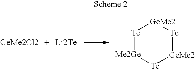
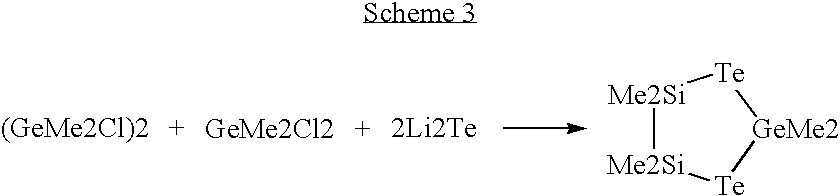
- precursors covered by general formulas (IIa), (IIb) and (IIc) include, but are not limited to: ((GeMe 2 )Te—) 3 ; ((GeEt 2 )Te—) 3 ; ((GeMeEt)Te—) 3 ; ((GeiPr 2 )Te—) 4 ; ((SiMe 2 )Te—) 3 ; ((SiEt 2 )Te—) 3 ; ((SiMeEt)Te—) 3 ; ((SiiPr 2 )Te—) 4 ; ((GeMe 2 ) 2 Te(GeMe 2 ) 2 Te—); ((GeMe 2 ) 3 Te—) 2 ; ((SiMe 2 ) 3 Te—) 2 ; ((SiMe 2 ) 3 Te—) 2 ; ((SiMe 2 ) 3 Te—) 2 ; ((SiMe
- the precursors can be shown schematically as:
- the precursors can be shown schematically as:
- precursors covered by general formulas (III) and (IV) include, but are not limited to: Te(GeNtBuCH 2 CH 2 NtBu); Te(GeNtBuCH ⁇ CHNtBu); Te((GeNtBuCH(CH 3 )CH(CH 3 )NtBu); Te(SiNtBuCH 2 CH 2 NtBu): Te(SiNtBuCH ⁇ CHNtBu); and Te((SiNtBuCH(CH 3 )CH(CH 3 )NtBu).
- Embodiments of the tellurium precursor may be synthesized in various ways. Examples of synthesis of the tellurium precursor include, but are not limited to synthesis schemes 1-5 as shown below:
- the disclosed precursors may be deposited to form a thin film using any deposition methods known to those of skill in the art.
- suitable deposition methods include without limitation, conventional CVD, atomic layer deposition (ALD), and pulsed chemical vapor deposition (P-CVD).
- a thermal CVD deposition is preferred.
- a precursor in vapor form is introduced into a reactor.
- the precursor in vapor form may be produced by vaporizing a liquid precursor solution, through a conventional vaporization step such as direct vaporization, distillation, or by bubbling an inert gas (e.g. N 2 , He, Ar, etc.) into the precursor solution and providing the inert gas plus precursor mixture as a precursor vapor solution to the reactor. Bubbling with an inert gas may also remove any dissolved oxygen present in the precursor solution.
- an inert gas e.g. N 2 , He, Ar, etc.
- the reactor contains one or more substrates on to which the thin films will be deposited.
- the one or more substrates may be any suitable substrate used in semiconductor, photovoltaic, flat panel, or LCD-TFT device manufacturing.
- suitable substrates include without limitation, silicon substrates, silica substrates, silicon nitride substrates, silicon oxy nitride substrates, tungsten substrates, or combinations thereof. Additionally, substrates comprising tungsten or noble metals (e.g. platinum, palladium, rhodium, or gold) may be used.
- Substrates may contain one or more additional layers of materials, which may be present from a previous manufacturing step. Dielectric and conductive layers are examples of these.
- the reactor or deposition chamber may be a heated vessel which has at least one or more substrates disposed within.
- the reactor has an outlet, which may be connected to a vacuum pump to allow by products to be removed from the chamber, or to allow the pressure within the reactor to be modified or regulated.
- the temperature in the chamber is normally maintained at a suitable temperature for the type of deposition process which is to be performed. In some cases, the chamber may be maintained at a lower temperature, for instance when the substrates themselves are heated directly, or where another energy source (e.g. plasma or radio frequency source) is provided to aid in the deposition.
- another energy source e.g. plasma or radio frequency source
- reactors include, without limitation, a cold-wall type reactor, a hot-wall type reactor, a single-wafer reactor, a multi-wafer reactor, or other types of deposition systems under conditions suitable to cause the precursors to react and form the layers.
- deposition may take place for a varying length of time. Generally, deposition may be allowed to continue as long as desired to produce a film with the necessary properties. Typical film thicknesses may vary from several hundred angstroms to several hundreds of microns, depending on the specific deposition process.
- the deposition chamber is maintained at a temperature greater than about 100° C. In some embodiments, the temperature is maintained between about 100° C. and about 500° C., preferably, between about 150° C. Likewise, the pressure in the deposition chamber is maintained at a pressure between about 1 Pa and about 10 5 Pa, and preferably between about 25 Pa, and about 10 3 Pa.
- a reducing gas is also introduced into the reaction chamber.
- the reducing gas may be one of hydrogen; ammonia; silane; disilane; trisilane; hydrogen radicals; and mixtures thereof.
- the germanium precursor and the reducing gas may be introduced to the reaction chamber substantially simultaneously.
- the germanium precursor and the reducing gas may be introduced sequentially, and in some cases, there may be an inert gas purge introduced between the precursor and reducing gas.
- germanium and antimony may also be provided and deposited on the substrate.
- a chalcogenide glass type film may be formed on the substrate, for instance, GeTe—Sb 2 Te 3 or Ge 2 Sb 2 Te 5 .
- the precursor and any optional reactants or precursors may be introduced sequentially (as in ALD) or simultaneously (as in CVD) into the reaction chamber.
- the reaction chamber is purged with an inert gas between the introduction of the precursor and the introduction of the reactant.
- the reactant and the precursor may be mixed together to form a reactant/precursor mixture, and then introduced to the reactor in mixture form.
- the precursor vapor solution and the reaction gas may be pulsed sequentially or simultaneously (e.g. pulsed CVD) into the reactor.
- Each pulse of precursor may last for a time period ranging from about 0.01 seconds to about 10 seconds, alternatively from about 0.3 seconds to about 3 seconds, alternatively from about 0.5 seconds to about 2 seconds.
- the reaction gas may also be pulsed into the reactor. In such embodiments, the pulse of each gas may last for a time period ranging from about 0.01 seconds to about 10 seconds, alternatively from about 0.3 seconds to about 3 seconds, alternatively from about 0.5 seconds to about 2 seconds.
- thermo-gravimetric analyses were performed in an inert atmosphere in order to avoid reaction of the molecules with air and moisture (same atmosphere encountered in the deposition process). The experiments were performed at atmospheric pressure.
- Te(SitBuMe 2 ) 2 is ranked second in terms of volatility, with a full evaporation at around 240° C.
- Te(SiiPr 3 ) 2 and Te(GeiPr 3 ) 2 exhibited roughly the same evaporation pattern, Te(GeiPr3)2 being slightly less volatile, which may be due to the heavy weight of germanium vs. silicon.
- the volatility and evaporation patterns of all these molecules fit to the criteria of CVD/ALD molecules.
Abstract
Description
(XR1R2R3)Te(XR4R5R6) (I)
(—(R1R2X)nTe—)y (IIa)
(—(R1R2X)nTe(XR3R4)m—)y (IIb)
(—(R1R2X)nTe(XR3R4)m)Te—)y (IIc)
Te(XNR1CR2R3CR4R5NR6) (III)
Te(XNR1CR2═CR3NR4) (IV)
wherein each of R1-6 is independently selected from among: H, a C1-C6 alkyl, a C1-C6 alkoxy, a C1-C6 alkylsilyl, a C1-C6 perfluorocarbon, a C1-C6 alkylsiloxy, a C1-C6 alkylamino, an alkylsilylamino, and an aminoamido; X is carbon, silicon or germanium; n and m are integers selected from 0, 1, and 2; in formulas (IIa) and (IIb), y is an integer selected from 2, 3 and 4; in formula (IIc), y is an integer selected from 1, 2 and 3. The tellurium containing precursor is introduced into the reactor. The reactor is maintained at a temperature of at least 100° C., and at least part of the precursor is deposited onto the substrate to form a tellurium containing film.
(XR1R2R3)Te(XR4R5R6) (I)
(—(R1R2X)nTe—)y (IIa)
(—(R1R2X)nTe(XR3R4)m—)y (IIb)
(—(R1R2X)nTe(XR3R4)m)Te—)y (IIC)
Te(XNR1CR2R3CR4R5NR6) (III)
Te(XNR1CR2═CR3NR4) (IV)
wherein each of R1-6 is independently selected from among: H, a C1-C6 alkyl, a C1-C6 alkoxy, a C1-C6 alkylsilyl, a C1-C6 perfluorocarbon, a C1-C6 alkylsiloxy, a C1-C6 alkylamino, an alkylsilylamino, and an aminoamido; X is carbon, silicon or germanium; n and m are integers selected from 0, 1, and 2; in formulas (IIa) and (IIb), y is an integer selected from 2, 3 and 4; in formula (IIc), y is an integer selected from 1, 2 and 3.
-
- maintaining the reactor at a temperature between about 100° C. and about 500° C., and preferably between about 150° C. and about 350° C.;
- maintaining the reactor at a pressure between about 1 Pa and about 105 Pa, and preferably between about 25 Pa and about 103 Pa;
- introducing at least one reducing gas into the reactor, wherein the reducing gas is at least one of: hydrogen; ammonia; silane; disilane; trisilane; hydrogen radicals; and mixtures thereof:
- the tellurium precursor and the reducing gas are introduced into the chamber either substantially simultaneously or sequentially;
- the tellurium precursor and the reducing gas are introduced into the chamber substantially simultaneously and the chamber is configured for chemical vapor deposition;
- the tellurium precursor and the reducing gas are introduced into the chamber sequentially and the chamber is configured for atomic layer deposition;
- a tellurium containing thin film coated substrate;
- introducing at least one germanium containing precursor and at least one antimony containing precursor; and depositing at least part of the germanium and antimony containing precursors onto the substrate to form a germanium, tellurium and antimony (GST) containing film; and
- the telluium precursor is at least one of: Te(GeMe3)2; Te(GeEt3)2; Te(GeiPr3)2; Te(GetBu3)2; Te(GetBuMe2)2; Te(SiMe3)2; Te(SiEt3)2; Te(SiiPr3)2; Te(SitBu3)2; Te(SitBuMe2)2; Te(Ge(SiMe3)3)2; Te(Si(SiMe3)3)2; Te(GeMe3)(Si(SiMe3)3), Te(Ge(SiMe3)3)2; ((GeMe2)Te—)3; ((GeEt2)Te—)3; ((GeMeEt)Te—)3; ((GeiPr2)Te—)4; ((SiMe2)Te—)3; ((SiEt2)Te—)3; ((SiMeEt)Te—)3; ((SiiPr2)Te—)4 ;((GeMe2)2Te(GeMe2)2Te—); ((GeMe2)3Te—)2; ((SiMe2)3Te—)2; CH2CH2GeMe2TeGeMe2—; SiMe2SiMe2GeMe2TeGeMe2—; Te(GeNtBuCH2CH2NtBu); Te(GeNtBuCH═CHNtBu); Te((GeNtBuCH(CH3)CH(CH3)NtBu); Te(SiNtBuCH2CH2NtBu); Te(SiNtBuCH═CHNtBu); and Te((SiNtBuCH(CH3)CH(CH3)NtBu).
(XR1R2R3)Te(XR4R5R6) (I)
(—(R1R2X)nTe—)y (IIa)
(—(R1R2X)nTe(XR3R4)m—)y (IIb)
(—(R1R2X)nTe(XR3R4)m)Te—)y (IIc)
Te(XNR1CR2R3CR4R5NR6) (III)
Te(XNR1CR2═CR3NR4) (IV)
wherein each of R1-6 is independently selected from among: H, a C1-C6 alkyl, a C1-C6 alkoxy, a C1-C6 alkylsilyl, a C1-C6 perfluorocarbon, a C1-C6 alkylsiloxy, a C1-C6 alkylamino, an alkylsilylamino, and an aminoamido; X is carbon, silicon or germanium; n and m are integers selected from 0, 1, and 2; in formulas (IIa) and (IIb), y is an integer selected from 2, 3 and 4; in formula (IIc), y is an integer selected from 1, 2 and 3.


Examples of precursors covered by general formulas (IIa), (IIb) and (IIc) include, but are not limited to: ((GeMe2)Te—)3; ((GeEt2)Te—)3; ((GeMeEt)Te—)3; ((GeiPr2)Te—)4; ((SiMe2)Te—)3; ((SiEt2)Te—)3; ((SiMeEt)Te—)3; ((SiiPr2)Te—)4; ((GeMe2)2Te(GeMe2)2Te—); ((GeMe2)3Te—)2; ((SiMe2)3Te—)2; CH2CH2GeMe2TeGeMe2—; and SiMe2SiMe2GeMe2TeGeMe2—.


Claims (10)
Priority Applications (7)
| Application Number | Priority Date | Filing Date | Title |
|---|---|---|---|
| CN200980119838XA CN102046838A (en) | 2008-05-29 | 2009-05-29 | Tellurium precursors for film deposition |
| KR1020107026546A KR20110014160A (en) | 2008-05-29 | 2009-05-29 | Tellurium precursors for film deposition |
| US12/475,204 US8101237B2 (en) | 2008-05-29 | 2009-05-29 | Tellurium precursors for film deposition |
| PCT/IB2009/008067 WO2010055423A2 (en) | 2008-05-29 | 2009-05-29 | Tellurium precursors for film deposition |
| JP2011511113A JP2011522120A (en) | 2008-05-29 | 2009-05-29 | Tellurium precursors for film deposition |
| TW098118134A TWI480411B (en) | 2008-05-29 | 2009-06-01 | Tellurium precursors for film deposition |
| US13/168,535 US8802194B2 (en) | 2008-05-29 | 2011-06-24 | Tellurium precursors for film deposition |
Applications Claiming Priority (2)
| Application Number | Priority Date | Filing Date | Title |
|---|---|---|---|
| US5712808P | 2008-05-29 | 2008-05-29 | |
| US12/475,204 US8101237B2 (en) | 2008-05-29 | 2009-05-29 | Tellurium precursors for film deposition |
Related Child Applications (1)
| Application Number | Title | Priority Date | Filing Date |
|---|---|---|---|
| US13/168,535 Continuation-In-Part US8802194B2 (en) | 2008-05-29 | 2011-06-24 | Tellurium precursors for film deposition |
Publications (2)
| Publication Number | Publication Date |
|---|---|
| US20090299084A1 US20090299084A1 (en) | 2009-12-03 |
| US8101237B2 true US8101237B2 (en) | 2012-01-24 |
Family
ID=41380625
Family Applications (1)
| Application Number | Title | Priority Date | Filing Date |
|---|---|---|---|
| US12/475,204 Active 2030-03-06 US8101237B2 (en) | 2008-05-29 | 2009-05-29 | Tellurium precursors for film deposition |
Country Status (6)
| Country | Link |
|---|---|
| US (1) | US8101237B2 (en) |
| JP (1) | JP2011522120A (en) |
| KR (1) | KR20110014160A (en) |
| CN (1) | CN102046838A (en) |
| TW (1) | TWI480411B (en) |
| WO (1) | WO2010055423A2 (en) |
Cited By (4)
| Publication number | Priority date | Publication date | Assignee | Title |
|---|---|---|---|---|
| US20120009731A1 (en) * | 2010-07-08 | 2012-01-12 | Keun Lee | Method of manufacturing phase-change random access memory |
| US20120021590A1 (en) * | 2008-05-29 | 2012-01-26 | L'air Liquide Societe Anonyme Pour I'etude Et I'exploitation Des Procedes Georges Claude | Tellurium Precursors for Film Deposition |
| US20120231611A1 (en) * | 2009-09-02 | 2012-09-13 | L'air Liquide Societe Anonyme Pour L'exploitation Des Procedes Georges Claude | Dihalide germanium(ii) precursors for germanium-containing film depositions |
| WO2021167776A1 (en) * | 2020-02-20 | 2021-08-26 | Applied Materials, Inc. | Deposition of tellurium-containing thin films |
Families Citing this family (18)
| Publication number | Priority date | Publication date | Assignee | Title |
|---|---|---|---|---|
| SG171683A1 (en) | 2006-05-12 | 2011-06-29 | Advanced Tech Materials | Low temperature deposition of phase change memory materials |
| WO2008057616A2 (en) | 2006-11-02 | 2008-05-15 | Advanced Technology Materials, Inc. | Antimony and germanium complexes useful for cvd/ald of metal thin films |
| KR101458953B1 (en) | 2007-10-11 | 2014-11-07 | 삼성전자주식회사 | Method of forming phase change material layer using Ge(Ⅱ) source, and method of fabricating phase change memory device |
| US8834968B2 (en) | 2007-10-11 | 2014-09-16 | Samsung Electronics Co., Ltd. | Method of forming phase change material layer using Ge(II) source, and method of fabricating phase change memory device |
| SG178736A1 (en) * | 2007-10-31 | 2012-03-29 | Advanced Tech Materials | Amorphous ge/te deposition process |
| US20090215225A1 (en) | 2008-02-24 | 2009-08-27 | Advanced Technology Materials, Inc. | Tellurium compounds useful for deposition of tellurium containing materials |
| WO2010055423A2 (en) | 2008-05-29 | 2010-05-20 | L'air Liquide - Societe Anonyme Pour I'etude Et I'exploitation Des Procedes Georges Claude | Tellurium precursors for film deposition |
| US8636845B2 (en) | 2008-06-25 | 2014-01-28 | L'Air Liquide, Société Anonyme pour l'Etude et l'Exploitation des Procédés Georges Claude | Metal heterocyclic compounds for deposition of thin films |
| WO2011095849A1 (en) * | 2010-02-03 | 2011-08-11 | L'air Liquide, Societe Anonyme Pour L'etude Et L'exploitation Des Procedes Georges Claude | Chalcogenide-containing precursors, methods of making, and methods of using the same for thin film deposition |
| KR102326396B1 (en) | 2013-09-27 | 2021-11-12 | 레르 리키드 쏘시에떼 아노님 뿌르 레드 에렉스뿔라따시옹 데 프로세데 조르즈 클로드 | Amine substituted trisilylamine and tridisilylamine compounds |
| US9543144B2 (en) * | 2014-12-31 | 2017-01-10 | L'air Liquide, Societe Anonyme Pour L'etude Et L'exploitation Des Procedes Georges Claude | Vapor deposition of chalcogenide-containing films |
| US9777025B2 (en) | 2015-03-30 | 2017-10-03 | L'Air Liquide, Société pour l'Etude et l'Exploitation des Procédés Georges Claude | Si-containing film forming precursors and methods of using the same |
| US11124876B2 (en) | 2015-03-30 | 2021-09-21 | L'Air Liquide, Société Anonyme pour l'Etude et l'Exploitation des Procédés Georges Claude | Si-containing film forming precursors and methods of using the same |
| US10192734B2 (en) | 2016-12-11 | 2019-01-29 | L'Air Liquide, Société Anonyme pour l'Etude et l'Exploration des Procédés Georges Claude | Short inorganic trisilylamine-based polysilazanes for thin film deposition |
| TW202026452A (en) * | 2018-10-04 | 2020-07-16 | 日商Adeka股份有限公司 | Thin film forming raw material for atomic layer deposition method, thin film forming raw material, method for producing thin film and compound |
| KR102444272B1 (en) * | 2020-05-18 | 2022-09-16 | 서울대학교산학협력단 | Method of forming chalcogenide-based thin film using atomic layer deposition process, method of forming switching device using the same and method of manufacturing memory device |
| KR102444266B1 (en) * | 2020-05-18 | 2022-09-16 | 서울대학교산학협력단 | Method of forming chalcogenide-based thin film using atomic layer deposition process, method of forming phase change material layer using the same and method of fabricating phase change memory device |
| CN115216748B (en) * | 2022-09-19 | 2022-12-30 | 中国科学院苏州纳米技术与纳米仿生研究所 | Preparation method of tellurium film and semiconductor device |
Citations (44)
| Publication number | Priority date | Publication date | Assignee | Title |
|---|---|---|---|---|
| US3573958A (en) | 1968-05-31 | 1971-04-06 | Francis E Small | Heat sensitive recording sheet |
| US4141778A (en) | 1976-02-12 | 1979-02-27 | Domrachev Georgy A | Method of preparing crystalline compounds AIVA BVIA |
| US4377613A (en) | 1981-09-14 | 1983-03-22 | Gordon Roy G | Non-iridescent glass structures |
| US4419386A (en) | 1981-09-14 | 1983-12-06 | Gordon Roy G | Non-iridescent glass structures |
| EP0568074A1 (en) | 1992-04-30 | 1993-11-03 | Consortium für elektrochemische Industrie GmbH | Process for the preparation of germanium dihalide ether adducts |
| DE4234998A1 (en) | 1992-10-16 | 1994-04-21 | Consortium Elektrochem Ind | New cyclic silicon and germanium amide cpds. - used in deposition of element which can be vaporised in vacuum or inert gas stream without decomposition, useful in semiconductor film prod |
| WO1996040448A1 (en) | 1995-06-07 | 1996-12-19 | Gordon Roy G | Process for the chemical vapor deposition of titanium and titanium nitride |
| WO1998016667A1 (en) | 1996-10-16 | 1998-04-23 | The President And Fellows Of Harvard College | Chemical vapor deposition of aluminum oxide |
| WO2000023635A1 (en) | 1998-10-21 | 2000-04-27 | The President And Fellows Of Harvard College | Liquid compounds for formation of materials containing alkaline earth metals |
| WO2000029637A1 (en) | 1998-11-12 | 2000-05-25 | President And Fellows Of Harvard College | Diffusion barrier materials with improved step coverage |
| WO2001066816A1 (en) | 2000-03-03 | 2001-09-13 | President And Fellows Of Harvard College | Liquid sources for cvd of group 6 metals and metal compounds |
| EP1180553A1 (en) | 2000-08-15 | 2002-02-20 | Air Products And Chemicals, Inc. | CVD process for depositing copper on a barrier layer |
| WO2002027063A2 (en) | 2000-09-28 | 2002-04-04 | President And Fellows Of Harward College | Vapor deposition of oxides, silicates and phosphates |
| WO2003083167A1 (en) | 2002-03-28 | 2003-10-09 | President And Fellows Of Harvard College | Vapor deposition of silicon dioxide nanolaminates |
| EP1464725A2 (en) | 2003-04-05 | 2004-10-06 | Rohm and Haas Electronic Materials, L.L.C. | Germanium compounds suitable for use in vapor deposition processes |
| EP1464724A2 (en) | 2003-04-05 | 2004-10-06 | Rohm and Haas Electronic Materials, L.L.C. | Organometallic compounds suitable for use in vapor deposition processes |
| US6984591B1 (en) | 2000-04-20 | 2006-01-10 | International Business Machines Corporation | Precursor source mixtures |
| US20060063394A1 (en) | 2004-09-22 | 2006-03-23 | Mcswiney Michael L | Precursors for film formation |
| US20060138393A1 (en) | 2004-12-27 | 2006-06-29 | Samsung Electronics Co., Ltd. | Ge precursor, GST thin layer formed using the same, phase-change memory device including the GST thin layer, and method of manufacturing the GST thin layer |
| US20060172067A1 (en) | 2005-01-28 | 2006-08-03 | Energy Conversion Devices, Inc | Chemical vapor deposition of chalcogenide materials |
| US20060172068A1 (en) | 2005-01-28 | 2006-08-03 | Ovshinsky Stanford R | Deposition of multilayer structures including layers of germanium and/or germanium alloys |
| US20060180811A1 (en) | 2005-02-14 | 2006-08-17 | Samsung Electronics Co., Ltd. | Precursor, thin layer prepared including the precursor, method of preparing the thin layer and phase-change memory device |
| US20060292301A1 (en) | 2005-06-22 | 2006-12-28 | Matrix Semiconductor, Inc. | Method of depositing germanium films |
| US20070054475A1 (en) | 2005-09-03 | 2007-03-08 | Jin-Il Lee | Method of forming a phase changeable material layer, a method of manufacturing a phase changeable memory unit, and a method of manufacturing a phase changeable semiconductor memory device |
| WO2007062096A2 (en) | 2005-11-23 | 2007-05-31 | The Arizona Board Of Regents, A Body Corporate Acting On Behalf Of Arizona State University | Silicon-germanium hydrides and methods for making and using same |
| WO2007067604A2 (en) | 2005-12-06 | 2007-06-14 | Structured Materials Inc. | Method of making undoped, alloyed and doped chalcogenide films by mocvd processes |
| EP1806427A2 (en) | 2006-01-10 | 2007-07-11 | Samsung Electronics Co., Ltd. | Method of forming phase change material thin film, and method of manufacturing phase change memory device using the same |
| WO2007133837A2 (en) | 2006-05-12 | 2007-11-22 | Advanced Technology Materials, Inc. | Low temperature deposition of phase change memory materials |
| WO2008002546A1 (en) | 2006-06-28 | 2008-01-03 | President And Fellows Of Harvard College | Metal(iv) tetra-amidinate compounds and their use in vapor deposition |
| US20080003359A1 (en) | 2006-06-28 | 2008-01-03 | President And Fellows Of Harvard College | Metal (IV) tetra-amidinate compounds and their use in vapor deposition |
| WO2008008319A2 (en) | 2006-07-10 | 2008-01-17 | President And Fellows Of Harvard College | Selective sealing of porous dielectric materials |
| US20080026577A1 (en) | 2006-07-31 | 2008-01-31 | Rohm And Haas Electronic Materials Llc | Organometallic compounds |
| US20080035906A1 (en) | 2006-07-13 | 2008-02-14 | Samsung Electronics Co., Ltd. | Germanium compound, semiconductor device fabricated using the same, and methods of forming the same |
| US20080096386A1 (en) | 2006-10-20 | 2008-04-24 | Samsung Electronics Co., Ltd. | Method of forming a phase-changeable layer and method of manufacturing a semiconductor memory device using the same |
| US20080108174A1 (en) | 2006-11-07 | 2008-05-08 | Samsung Electronics Co., Ltd. | Metal precursors for low temperature deposition and methods of forming a metal thin layer and manufacturing a phase-change memory device using the metal precursors |
| WO2008057616A2 (en) | 2006-11-02 | 2008-05-15 | Advanced Technology Materials, Inc. | Antimony and germanium complexes useful for cvd/ald of metal thin films |
| US20080118636A1 (en) | 2006-11-21 | 2008-05-22 | Samsung Electronics Co., Ltd | Method of forming phase change layer using a germanium precursor and method of manufacturing phase change memory device using the same |
| EP1995236A1 (en) | 2007-04-24 | 2008-11-26 | Air Products and Chemicals, Inc. | Tellurium (Te) precursors for making phase change memory materials |
| WO2009039187A1 (en) | 2007-09-17 | 2009-03-26 | L'air Liquide - Societe Anonyme Pour L'etude Et L'exploitation Des Procedes Georges Claude | Tellurium precursors for gst film deposition |
| US20090137100A1 (en) * | 2007-11-27 | 2009-05-28 | Air Products And Chemicals, Inc. | Tellurium Precursors for GST Films in an ALD or CVD Process |
| WO2009081383A1 (en) | 2007-12-21 | 2009-07-02 | L'air Liquide-Societe Anonyme Pour L'etude Et L'exploitation Des Procedes Georges Claude | Germanium precursors for gst film deposition |
| WO2009132207A2 (en) | 2008-04-25 | 2009-10-29 | Asm International N.V. | Synthesis and use of precursors for ald of tellurium and selenium thin films |
| US20090280052A1 (en) | 2008-05-08 | 2009-11-12 | Air Products And Chemicals, Inc. | Binary and Ternary Metal Chalcogenide Materials and Method of Making and Using Same |
| US20090299084A1 (en) | 2008-05-29 | 2009-12-03 | Okubo Shingo | Tellurium precursors for film deposition |
Family Cites Families (2)
| Publication number | Priority date | Publication date | Assignee | Title |
|---|---|---|---|---|
| US7630142B2 (en) * | 2006-10-20 | 2009-12-08 | Olympus Imaging Corp. | Bent type zoom optical system and imaging system using the same |
| TWM372771U (en) * | 2009-05-20 | 2010-01-21 | Legend Lifestyle Products Corp | Torque detection display device for tool |
-
2009
- 2009-05-29 WO PCT/IB2009/008067 patent/WO2010055423A2/en active Application Filing
- 2009-05-29 KR KR1020107026546A patent/KR20110014160A/en not_active Application Discontinuation
- 2009-05-29 JP JP2011511113A patent/JP2011522120A/en active Pending
- 2009-05-29 CN CN200980119838XA patent/CN102046838A/en active Pending
- 2009-05-29 US US12/475,204 patent/US8101237B2/en active Active
- 2009-06-01 TW TW098118134A patent/TWI480411B/en not_active IP Right Cessation
Patent Citations (48)
| Publication number | Priority date | Publication date | Assignee | Title |
|---|---|---|---|---|
| US3573958A (en) | 1968-05-31 | 1971-04-06 | Francis E Small | Heat sensitive recording sheet |
| US4141778A (en) | 1976-02-12 | 1979-02-27 | Domrachev Georgy A | Method of preparing crystalline compounds AIVA BVIA |
| US4377613A (en) | 1981-09-14 | 1983-03-22 | Gordon Roy G | Non-iridescent glass structures |
| WO1983001018A1 (en) | 1981-09-14 | 1983-03-31 | Roy Gerald Gordon | Non-iridescent glass structures |
| US4419386A (en) | 1981-09-14 | 1983-12-06 | Gordon Roy G | Non-iridescent glass structures |
| EP0568074A1 (en) | 1992-04-30 | 1993-11-03 | Consortium für elektrochemische Industrie GmbH | Process for the preparation of germanium dihalide ether adducts |
| DE4234998A1 (en) | 1992-10-16 | 1994-04-21 | Consortium Elektrochem Ind | New cyclic silicon and germanium amide cpds. - used in deposition of element which can be vaporised in vacuum or inert gas stream without decomposition, useful in semiconductor film prod |
| US5656338A (en) | 1994-12-13 | 1997-08-12 | Gordon; Roy G. | Liquid solution of TiBr4 in Br2 used as a precursor for the chemical vapor deposition of titanium or titanium nitride |
| WO1996040448A1 (en) | 1995-06-07 | 1996-12-19 | Gordon Roy G | Process for the chemical vapor deposition of titanium and titanium nitride |
| WO1998016667A1 (en) | 1996-10-16 | 1998-04-23 | The President And Fellows Of Harvard College | Chemical vapor deposition of aluminum oxide |
| WO2000023635A1 (en) | 1998-10-21 | 2000-04-27 | The President And Fellows Of Harvard College | Liquid compounds for formation of materials containing alkaline earth metals |
| WO2000029637A1 (en) | 1998-11-12 | 2000-05-25 | President And Fellows Of Harvard College | Diffusion barrier materials with improved step coverage |
| WO2001066816A1 (en) | 2000-03-03 | 2001-09-13 | President And Fellows Of Harvard College | Liquid sources for cvd of group 6 metals and metal compounds |
| US6984591B1 (en) | 2000-04-20 | 2006-01-10 | International Business Machines Corporation | Precursor source mixtures |
| EP1180553A1 (en) | 2000-08-15 | 2002-02-20 | Air Products And Chemicals, Inc. | CVD process for depositing copper on a barrier layer |
| WO2002027063A2 (en) | 2000-09-28 | 2002-04-04 | President And Fellows Of Harward College | Vapor deposition of oxides, silicates and phosphates |
| WO2003083167A1 (en) | 2002-03-28 | 2003-10-09 | President And Fellows Of Harvard College | Vapor deposition of silicon dioxide nanolaminates |
| EP1464725A2 (en) | 2003-04-05 | 2004-10-06 | Rohm and Haas Electronic Materials, L.L.C. | Germanium compounds suitable for use in vapor deposition processes |
| EP1464724A2 (en) | 2003-04-05 | 2004-10-06 | Rohm and Haas Electronic Materials, L.L.C. | Organometallic compounds suitable for use in vapor deposition processes |
| US7413776B2 (en) | 2003-04-05 | 2008-08-19 | Rohm And Haas Electronic Materials Llc | Method of depositing a metal-containing film |
| US20060063394A1 (en) | 2004-09-22 | 2006-03-23 | Mcswiney Michael L | Precursors for film formation |
| US20060138393A1 (en) | 2004-12-27 | 2006-06-29 | Samsung Electronics Co., Ltd. | Ge precursor, GST thin layer formed using the same, phase-change memory device including the GST thin layer, and method of manufacturing the GST thin layer |
| US20060172067A1 (en) | 2005-01-28 | 2006-08-03 | Energy Conversion Devices, Inc | Chemical vapor deposition of chalcogenide materials |
| US20060172068A1 (en) | 2005-01-28 | 2006-08-03 | Ovshinsky Stanford R | Deposition of multilayer structures including layers of germanium and/or germanium alloys |
| US20060180811A1 (en) | 2005-02-14 | 2006-08-17 | Samsung Electronics Co., Ltd. | Precursor, thin layer prepared including the precursor, method of preparing the thin layer and phase-change memory device |
| US20060292301A1 (en) | 2005-06-22 | 2006-12-28 | Matrix Semiconductor, Inc. | Method of depositing germanium films |
| US20070054475A1 (en) | 2005-09-03 | 2007-03-08 | Jin-Il Lee | Method of forming a phase changeable material layer, a method of manufacturing a phase changeable memory unit, and a method of manufacturing a phase changeable semiconductor memory device |
| WO2007062096A2 (en) | 2005-11-23 | 2007-05-31 | The Arizona Board Of Regents, A Body Corporate Acting On Behalf Of Arizona State University | Silicon-germanium hydrides and methods for making and using same |
| WO2007067604A2 (en) | 2005-12-06 | 2007-06-14 | Structured Materials Inc. | Method of making undoped, alloyed and doped chalcogenide films by mocvd processes |
| EP1806427A2 (en) | 2006-01-10 | 2007-07-11 | Samsung Electronics Co., Ltd. | Method of forming phase change material thin film, and method of manufacturing phase change memory device using the same |
| WO2007133837A2 (en) | 2006-05-12 | 2007-11-22 | Advanced Technology Materials, Inc. | Low temperature deposition of phase change memory materials |
| WO2008002546A1 (en) | 2006-06-28 | 2008-01-03 | President And Fellows Of Harvard College | Metal(iv) tetra-amidinate compounds and their use in vapor deposition |
| US20080003359A1 (en) | 2006-06-28 | 2008-01-03 | President And Fellows Of Harvard College | Metal (IV) tetra-amidinate compounds and their use in vapor deposition |
| WO2008008319A2 (en) | 2006-07-10 | 2008-01-17 | President And Fellows Of Harvard College | Selective sealing of porous dielectric materials |
| US20080035906A1 (en) | 2006-07-13 | 2008-02-14 | Samsung Electronics Co., Ltd. | Germanium compound, semiconductor device fabricated using the same, and methods of forming the same |
| US20080026577A1 (en) | 2006-07-31 | 2008-01-31 | Rohm And Haas Electronic Materials Llc | Organometallic compounds |
| US20080096386A1 (en) | 2006-10-20 | 2008-04-24 | Samsung Electronics Co., Ltd. | Method of forming a phase-changeable layer and method of manufacturing a semiconductor memory device using the same |
| WO2008057616A2 (en) | 2006-11-02 | 2008-05-15 | Advanced Technology Materials, Inc. | Antimony and germanium complexes useful for cvd/ald of metal thin films |
| US20080108174A1 (en) | 2006-11-07 | 2008-05-08 | Samsung Electronics Co., Ltd. | Metal precursors for low temperature deposition and methods of forming a metal thin layer and manufacturing a phase-change memory device using the metal precursors |
| US20080118636A1 (en) | 2006-11-21 | 2008-05-22 | Samsung Electronics Co., Ltd | Method of forming phase change layer using a germanium precursor and method of manufacturing phase change memory device using the same |
| EP1995236A1 (en) | 2007-04-24 | 2008-11-26 | Air Products and Chemicals, Inc. | Tellurium (Te) precursors for making phase change memory materials |
| US20090142881A1 (en) | 2007-04-24 | 2009-06-04 | Air Products And Chemicals, Inc. | Tellurium (Te) Precursors for Making Phase Change Memory Materials |
| WO2009039187A1 (en) | 2007-09-17 | 2009-03-26 | L'air Liquide - Societe Anonyme Pour L'etude Et L'exploitation Des Procedes Georges Claude | Tellurium precursors for gst film deposition |
| US20090137100A1 (en) * | 2007-11-27 | 2009-05-28 | Air Products And Chemicals, Inc. | Tellurium Precursors for GST Films in an ALD or CVD Process |
| WO2009081383A1 (en) | 2007-12-21 | 2009-07-02 | L'air Liquide-Societe Anonyme Pour L'etude Et L'exploitation Des Procedes Georges Claude | Germanium precursors for gst film deposition |
| WO2009132207A2 (en) | 2008-04-25 | 2009-10-29 | Asm International N.V. | Synthesis and use of precursors for ald of tellurium and selenium thin films |
| US20090280052A1 (en) | 2008-05-08 | 2009-11-12 | Air Products And Chemicals, Inc. | Binary and Ternary Metal Chalcogenide Materials and Method of Making and Using Same |
| US20090299084A1 (en) | 2008-05-29 | 2009-12-03 | Okubo Shingo | Tellurium precursors for film deposition |
Non-Patent Citations (51)
Cited By (7)
| Publication number | Priority date | Publication date | Assignee | Title |
|---|---|---|---|---|
| US20120021590A1 (en) * | 2008-05-29 | 2012-01-26 | L'air Liquide Societe Anonyme Pour I'etude Et I'exploitation Des Procedes Georges Claude | Tellurium Precursors for Film Deposition |
| US8802194B2 (en) * | 2008-05-29 | 2014-08-12 | L'Air Liquide, Société Anonyme pour l'Etude et l'Exploitation des Procédés Georges Claude | Tellurium precursors for film deposition |
| US20120231611A1 (en) * | 2009-09-02 | 2012-09-13 | L'air Liquide Societe Anonyme Pour L'exploitation Des Procedes Georges Claude | Dihalide germanium(ii) precursors for germanium-containing film depositions |
| US8691668B2 (en) * | 2009-09-02 | 2014-04-08 | L'Air Liquide, Société Anonyme pour l'Etude et l'Exploitation des Procédés Georges Claude | Dihalide germanium(II) precursors for germanium-containing film depositions |
| US20120009731A1 (en) * | 2010-07-08 | 2012-01-12 | Keun Lee | Method of manufacturing phase-change random access memory |
| WO2021167776A1 (en) * | 2020-02-20 | 2021-08-26 | Applied Materials, Inc. | Deposition of tellurium-containing thin films |
| US11408068B2 (en) | 2020-02-20 | 2022-08-09 | Applied Materials, Inc. | Deposition of tellurium-containing thin films |
Also Published As
| Publication number | Publication date |
|---|---|
| US20090299084A1 (en) | 2009-12-03 |
| TWI480411B (en) | 2015-04-11 |
| KR20110014160A (en) | 2011-02-10 |
| WO2010055423A8 (en) | 2010-09-02 |
| WO2010055423A3 (en) | 2010-07-15 |
| TW201016877A (en) | 2010-05-01 |
| WO2010055423A2 (en) | 2010-05-20 |
| JP2011522120A (en) | 2011-07-28 |
| CN102046838A (en) | 2011-05-04 |
Similar Documents
| Publication | Publication Date | Title |
|---|---|---|
| US8101237B2 (en) | Tellurium precursors for film deposition | |
| US8193388B2 (en) | Compounds for depositing tellurium-containing films | |
| US8454928B2 (en) | Tellurium precursors for GST deposition | |
| US20090162973A1 (en) | Germanium precursors for gst film deposition | |
| EP2242870B1 (en) | Method using new metal precursors containing beta-diketiminato ligands | |
| US8802194B2 (en) | Tellurium precursors for film deposition | |
| US8357614B2 (en) | Ruthenium-containing precursors for CVD and ALD | |
| KR101602984B1 (en) | Niobium and vanadium organometallic precursors for thin film deposition | |
| US8318252B2 (en) | Antimony precursors for GST films in ALD/CVD processes | |
| KR102219147B1 (en) | Group 5 transition metal-containing compounds for vapor deposition of group 5 transition metal-containing films | |
| US9240319B2 (en) | Chalcogenide-containing precursors, methods of making, and methods of using the same for thin film deposition | |
| US20110262660A1 (en) | Chalcogenide-containing precursors, methods of making, and methods of using the same for thin film deposition | |
| US10023462B2 (en) | Niobium-Nitride film forming compositions and vapor deposition of Niobium-Nitride films | |
| US8686138B2 (en) | Heteroleptic pyrrolecarbaldimine precursors | |
| EP4301896A1 (en) | Reagents to remove oxygen from metal oxyhalide precursors in thin film deposition processes | |
| US20220372053A1 (en) | Stable bis(alkyl-arene) transition metal complexes and methods of film deposition using the same | |
| US20210032275A1 (en) | Cyclic germanium silylamido precursors for ge-containing film depositions and methods of using the same | |
| US20220106333A1 (en) | Indium precursors for vapor depositions | |
| EP2540733A1 (en) | Deposition of indium containing thin films using new indium precursors | |
| EP2492272A1 (en) | Deposition of indium containing thin films using indium alkylamide precursor | |
| EP4061978A1 (en) | Compounds and methods for selectively forming metal-containing films | |
| TW202337892A (en) | Alkyl and aryl heteroleptic bismuth precursors for bismuth oxide containing thin films | |
| US8431719B1 (en) | Heteroleptic pyrrolecarbaldimine precursors | |
| EP2540732A1 (en) | Deposition of gallium containing thin films using new gallium precursors. |
Legal Events
| Date | Code | Title | Description |
|---|---|---|---|
| AS | Assignment |
Owner name: L'AIR LIQUIDE, SOCIETE ANONYME POUR L'ETUDE ET L'E Free format text: ASSIGNMENT OF ASSIGNORS INTEREST;ASSIGNORS:OKUBO, SHINGO;YANAGITA, KAZUTAKA;GATINEAU, JULIEN;REEL/FRAME:022992/0322 Effective date: 20090224 |
|
| AS | Assignment |
Owner name: L'AIR LIQUIDE SOCIETE ANONYME POUR L'ETUDE ET L'EX Free format text: ASSIGNMENT OF ASSIGNORS INTEREST;ASSIGNORS:OKUBO, SHINGO;YANAGITA, KAZUTAKA;GATINEAU, JULIEN;SIGNING DATES FROM 20101112 TO 20101115;REEL/FRAME:025362/0445 |
|
| STCF | Information on status: patent grant |
Free format text: PATENTED CASE |
|
| AS | Assignment |
Owner name: L'AIR LIQUIDE, SOCIETE ANONYME POUR L'ETUDE ET L'E Free format text: ASSIGNMENT OF ASSIGNORS INTEREST;ASSIGNOR:MINOURA, MAO;REEL/FRAME:027528/0349 Effective date: 20111129 |
|
| FEPP | Fee payment procedure |
Free format text: PAYOR NUMBER ASSIGNED (ORIGINAL EVENT CODE: ASPN); ENTITY STATUS OF PATENT OWNER: LARGE ENTITY |
|
| FPAY | Fee payment |
Year of fee payment: 4 |
|
| MAFP | Maintenance fee payment |
Free format text: PAYMENT OF MAINTENANCE FEE, 8TH YEAR, LARGE ENTITY (ORIGINAL EVENT CODE: M1552); ENTITY STATUS OF PATENT OWNER: LARGE ENTITY Year of fee payment: 8 |
|
| MAFP | Maintenance fee payment |
Free format text: PAYMENT OF MAINTENANCE FEE, 12TH YEAR, LARGE ENTITY (ORIGINAL EVENT CODE: M1553); ENTITY STATUS OF PATENT OWNER: LARGE ENTITY Year of fee payment: 12 |