US8090269B2 - Data transmission system and transmission code generating method for the same - Google Patents
Data transmission system and transmission code generating method for the same Download PDFInfo
- Publication number
- US8090269B2 US8090269B2 US12/007,846 US784608A US8090269B2 US 8090269 B2 US8090269 B2 US 8090269B2 US 784608 A US784608 A US 784608A US 8090269 B2 US8090269 B2 US 8090269B2
- Authority
- US
- United States
- Prior art keywords
- phase
- signal
- signal points
- data
- transmission
- Prior art date
- Legal status (The legal status is an assumption and is not a legal conclusion. Google has not performed a legal analysis and makes no representation as to the accuracy of the status listed.)
- Expired - Fee Related, expires
Links
- 230000005540 biological transmission Effects 0.000 title claims abstract description 82
- 238000000034 method Methods 0.000 title claims description 15
- 238000001514 detection method Methods 0.000 claims abstract description 9
- 238000012937 correction Methods 0.000 claims abstract description 6
- 238000000638 solvent extraction Methods 0.000 claims abstract 2
- 230000010363 phase shift Effects 0.000 claims description 39
- 230000003287 optical effect Effects 0.000 claims description 30
- 238000007476 Maximum Likelihood Methods 0.000 claims 1
- 230000003111 delayed effect Effects 0.000 description 20
- 238000006243 chemical reaction Methods 0.000 description 7
- 238000005516 engineering process Methods 0.000 description 7
- 238000010586 diagram Methods 0.000 description 4
- 238000004891 communication Methods 0.000 description 3
- 238000012986 modification Methods 0.000 description 2
- 230000004048 modification Effects 0.000 description 2
- 239000013307 optical fiber Substances 0.000 description 2
- 230000007704 transition Effects 0.000 description 2
- 230000006866 deterioration Effects 0.000 description 1
- 230000000694 effects Effects 0.000 description 1
- 238000002474 experimental method Methods 0.000 description 1
- 238000005192 partition Methods 0.000 description 1
- 230000002269 spontaneous effect Effects 0.000 description 1
- 230000001360 synchronised effect Effects 0.000 description 1
Images


Classifications
-
- H—ELECTRICITY
- H04—ELECTRIC COMMUNICATION TECHNIQUE
- H04B—TRANSMISSION
- H04B10/00—Transmission systems employing electromagnetic waves other than radio-waves, e.g. infrared, visible or ultraviolet light, or employing corpuscular radiation, e.g. quantum communication
- H04B10/50—Transmitters
- H04B10/516—Details of coding or modulation
- H04B10/548—Phase or frequency modulation
- H04B10/556—Digital modulation, e.g. differential phase shift keying [DPSK] or frequency shift keying [FSK]
- H04B10/5561—Digital phase modulation
-
- H—ELECTRICITY
- H04—ELECTRIC COMMUNICATION TECHNIQUE
- H04B—TRANSMISSION
- H04B10/00—Transmission systems employing electromagnetic waves other than radio-waves, e.g. infrared, visible or ultraviolet light, or employing corpuscular radiation, e.g. quantum communication
- H04B10/50—Transmitters
- H04B10/501—Structural aspects
- H04B10/503—Laser transmitters
- H04B10/505—Laser transmitters using external modulation
- H04B10/5055—Laser transmitters using external modulation using a pre-coder
-
- H—ELECTRICITY
- H04—ELECTRIC COMMUNICATION TECHNIQUE
- H04B—TRANSMISSION
- H04B10/00—Transmission systems employing electromagnetic waves other than radio-waves, e.g. infrared, visible or ultraviolet light, or employing corpuscular radiation, e.g. quantum communication
- H04B10/60—Receivers
- H04B10/66—Non-coherent receivers, e.g. using direct detection
- H04B10/67—Optical arrangements in the receiver
- H04B10/676—Optical arrangements in the receiver for all-optical demodulation of the input optical signal
- H04B10/677—Optical arrangements in the receiver for all-optical demodulation of the input optical signal for differentially modulated signal, e.g. DPSK signals
Definitions
- This invention relates to a transmitter and a receiver for performing data transmission via a data communication path, and more particularly to an encoder/decoder capable of suppressing an occurrence of an error in a receiver in optical phase shift keying modulated transmission.
- BPSK binary phase shift keying
- QPSK quadrature phase shift keying
- nASK n-ary amplitude shift keying
- the quadrature phase shift keying (QPSK) modulated transmission is an example of optical many valued phase shift keying modulated transmission.
- QPSK modulated transmission is a transmission method in which, signal points (P 1 , P 2 , P 3 , and P 4 ) are arranged at phase intervals of ⁇ /2 radian in one cycle (2 ⁇ radian) of the same amplitude and carrier on a complex plane I-Q indicating signals corresponding to 1 symbol (see, OFC/NFOEC 2006, PDP36, 100 Gbit/s DQPSK Transmission Experiment without OTDM for 100G Ethernet Transport, hereinafter referred to as Non-Patent Document 1).
- the implementation of higher-order PSK has also been devised, as 8-ary phase shift keying (8PSK) modulation and 16-ary phase shift keying (16PSK) modulation.
- the data when input serial data is indefinite in appearance frequency of 0 and 1 in number of successive bits, the data is partitioned into units of 8 bits so as to make the appearance frequencies of 0 and 1 equal to each other at relatively short bit intervals (several tens of bits) while limiting the number of successive bits to 5 at maximum.
- Non-patent Document 2 discloses, as another transmission code different from the above, the application of a 64B/66B transmission code.
- input serial data is partitioned into units of 64 bits, and each 64 bits of data is provided with 2 bits of header information while the 64 bits of data other than the header information is scrambled, to thereby make the appearance frequencies of 0 and 1 stochastically equal to each other, which makes it possible to achieve DC balance on a transmission path.
- the 2 bits of header information only include “01” and “10” so as to limit the successive equivalent bits to a finite number.
- a transmitter converts binary bit data into phase information, and further transmits the data by converting an electric signal to an optical signal. Then, a receiver performs delayed modulation by a symbol delayed Mach-Zehnder interferometer with respect to the received optical signal, and converts the optical signal into binary bit data.
- phase noise is caused in a source of laser to be input to a modulation circuit of the transmitter.
- the phase noise is generated due to amplified spontaneous emission light from a laser oscillator, which is a short-cycle noise having a frequency characteristic of the order of picoseconds.
- the receiver performs demodulation through delayed modulation by a symbol delayed Mach-Zehnder interferometer.
- the phase difference between signal points is converted into an output voltage amplitude of a photodiode, and therefore the phase noise of the light source becomes an amplitude noise in the output voltage. Accordingly, along with an increase in number of signal points in a phase direction, it becomes more difficult to discriminate the signal points from one another, which hinders increase in number of signal points.
- the above-mentioned problem is unique to the optical phase shift keying modulation. This problem does not occur in a wireless or wired electric transmission, because a phase noise generated in a carrier is small enough to be ignored and the receiver performs synchronous detection because it facilitates phase synchronization.
- the wireless transmission there occurs a problem that all the signal points have the same phase fluctuation due to an influence from a propagation path.
- the phase fluctuation in the wireless transmission is a phase noise having a frequency characteristic of short cycle, which is caused when the location of the transmitter or the receiver has changed.
- an optical fibre which is used as the propagation path, is stable in characteristic, and therefore the above-mentioned problem does not occur.
- Patent Document 1 and Non-patent Document 2 in which an 8B/10B code and a 64B/66B code are used, respectively, no consideration is given to the phase noise to be caused in the optical phase shift keying modulated transmission, and therefore the error rate due to the phase noise significantly increases when the number of phases is increased. It is an object of this invention to provide a technology capable of reducing the influence of the phase noise caused in the light source when the number of phases (number of signals) is increased in the optical phase shift keying modulated transmission while allowing the receiver to detect and correct an error.
- N signal points (P 1 , P 2 , . . . , PN) are arranged at equal phase intervals on a complex plane I-Q which indicates signals corresponding to 1 symbol.
- the signal points are arranged in one cycle (2 ⁇ radian) of the same amplitude and carrier.
- This optical many valued phase shift keying modulation is referred to as N-ary phase shift keying modulation.
- the intervals between the signal points are equal to one another in a phase direction, however, the intervals between the signal points according to this invention is not limited thereto.
- This invention provides a data transmission system including a transmitter and a receiver which are coupled to each other through a transmission path.
- the data transmission system transmits data of transmitting by converting the data into an optical signal.
- the transmitter includes a phase encoder for converting input binary data into signal points for optical phase shift keying modulation (in other words, transmission phase information), a differential pre-coder for performing differential coding of the transmission phase, a laser generation for generating a laser of predetermined single wavelength to output a carrier, and a phase shift keying modulator for outputting an optical signal obtained through phase modulation based on the carrier and the transmission phase of an electric signal.
- the receiver includes a delayed modulator for detecting a phase difference between symbols from the received optical signal and converting the phase difference into the phase information of the electric signal, and a phase decoder for converting the received phase information into binary data.
- the transmitter according to this invention defines, based on a symbol which has been currently transmitted, a signal point to be transmitted at the next symbol in the time axis direction, and transmits the signal point thus defined. In other words, in a case where a signal point P 1 has been transmitted at a certain point in time, the transmission of any one of signal points P 1 to PN is prohibited at the next point in time.
- this invention is capable of reducing a region where the error probability distribution is overlapped between two signal points, with the result that the symbol error rate in the demodulator (that is, demodulator) and in the phase decoder of the receiver is reduced.
- the above-mentioned process is referred to as the limitation of signal point transition.
- the 8-ary phase shift keying (8PSK) modulation includes eight signal points P 1 to P 8 .
- the signal points P 1 to P 8 are arranged on a complex plane in order of P 1 , P 2 , P 3 , P 4 , P 5 , P 6 , P 7 , and P 8 , so as to be adjacent to one another in a phase direction. At this time, the signal points P 1 and P 8 are arranged adjacent to each other as one cycle is completed.
- the signal point intervals may be set twice as large as the minimum interval.
- the signal point intervals are set such that at least one of the intervals is set three times larger than the minimum interval.
- the total sum of all the signal point intervals between the used signal points corresponds to one cycle (2 ⁇ radian).
- an interval of signal points to be transmitted next is obtained by a combination of ⁇ 3 ⁇ /4, 2 ⁇ /4, 3 ⁇ 4 ⁇ , and three signal points P 1 , P 4 , and P 6 can be used (hereinafter, for the sake of convenience, ⁇ 3 ⁇ /4, 2 ⁇ /4, 3 ⁇ 4 ⁇ is referred to as ⁇ 3, 2, 3 ⁇ ).
- the combination of the above-mentioned intervals of signal points is not limited thereto, and may include ⁇ 2, 3, 3 ⁇ and ⁇ 3, 3, 2).
- a combination of intervals between signal points that can allow a maximum number of signal points to be used is ⁇ 3, 2, 2, 2, 2, 2, 3 ⁇ , and when the current symbol is a signal point P 1 , the signal points that can be used next are P 1 , P 4 , P 6 , P 8 , P 10 , P 12 , and P 14 .
- the combination of intervals of signal points is not limited thereto.
- the maximum number M of signal points that can be used in N-ary phase shift keying modulation signal (N is a natural number) is determined as follows.
- phase encoder of the transmitter In the phase encoder of the transmitter according to this invention, binary bit data to be transmitted is converted into phase information for phase shift keying modulation. As a specific example thereof, 3 bits of binary data can be converted into 2 symbols of 8-ary phase information, which are associated with each other, for example, as shown in FIG. 4 . Similarly, the phase decoder of the receiver inversely converts the received phase information to the corresponding binary bit data.
- the transmitter according to this invention uses only three signal points of the eight signal points in 8-ary phase shift keying modulated transmission.
- the signal points that can be used are arranged at intervals which are at least two times or three times the minimum signal point interval.
- the delayed modulator has converted an optical signal into an electric signal of phase information
- the detection can be determined as being an error because the signal at the signal point P 5 is not supposed to be used.
- the phase information thus detected can be determined as being incorrect, and it is possible to perform an error correction by changing the signal point P 3 to the signal point P 4 because the hamming distance from the signal point P 4 is 1 and the hamming distance from the signal point P 1 is 2.
- FIG. 1 is a block diagram illustrating a configuration of a data transmission system which is common to a first embodiment and a second embodiment of this invention
- FIG. 2 is a diagram illustrating a signal point arrangement of transitional signal points in an 8-ary phase shift keying modulated transmission used in the data transmission system of the first embodiment
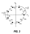
- FIG. 3 is a diagram illustrating a signal point arrangement of transitional signal points in an 16-ary phase shift keying modulated transmission used in the data transmission system of the second embodiment.
- FIG. 4 is an explanatory diagram showing binary data of 3 bits and 8-ary phase information of 2 symbols.
- the data transmission system includes, for example, as shown in FIG. 1 , a transmitter 1 , a transmission path 2 , and a receiver 3 .
- the transmitter 1 is coupled to the receiver 3 via the transmission path 2 .
- Data of transmitting 10 which is to be transmitted, input to the transmitter 1 is subjected to desired data conversion, and output to the transmission path 2 .
- the receiver 3 subjects the received data to desired data conversion, and outputs the data as received data 33 .
- the data of transmitting 10 and the received data 33 have the same value, as long as a transmission error in the transmission path 2 is occurring within the error correction capability of the data transmission system.
- the transmitter 1 includes a phase encoder 11 , a differential pre-coder 12 , a laser oscillator 13 , and a phase shift keying modulator 14 .
- the data of transmitting 10 is input to the phase encoder 11 , and an output from the phase encoder 11 is coupled to the differential pre-coder 12 .
- An output from the differential pre-coder 12 and an output from the laser oscillator 13 are coupled to the phase shift keying modulator 14 , while an output from the phase shift keying modulator 14 is coupled to the transmission path 2 .
- the receiver 3 includes a delayed modulator 30 and a phase decoder 32 .
- the transmission path 2 is coupled to the delayed modulator 30
- an output from the delayed modulator 30 is coupled to the phase decoder 32 .
- the phase decoder 32 outputs the received data 33 .
- the data of transmitting 10 includes time-consecutive binary bit data.
- the data of transmitting 10 is first input to the phase encoder 11 .
- the phase encoder 11 partitions the data of transmitting 10 , which includes a time-consecutive bit string, into blocks each formed of an equal number of bits, and converts each of the blocks into corresponding phase information.
- the phase information is expressed by selectively using only limited signal points, rather than using all the signal points that can be output by the phase shift keying modulator 14 .
- a description will be given of a conversion method in which the data of transmitting 10 is partitioned into blocks in units of 3 bits, and further converted into phase information of 2 symbols which is uniquely determined based on the value of each block.
- 1 symbol includes eight signal points (from P 1 to P 8 ) as shown in FIG. 2 , which are sequentially arranged in a phase direction, and only three signal points (P 1 , P 4 , an P 6 ) of the eight signal points are used.
- the table 1 or the like is used for associating the bit string and the phase information with each other.
- the phase encoder 11 outputs the phase information after conversion, for each of successive symbols.
- the phase information output by the phase encoder 11 is input to the differential pre-coder 12 .
- the differential pre-coder 12 calculates the difference between the phase information output at 1 symbol before and the input phase information to perform differential coding, and outputs the difference as phase difference information. It is determined as to whether it is necessary or not to provide the differential pre-coder 12 depending on the detection method in the receiver 3 . In a case where the detection method is a delayed modulation by a symbol delayed Mach-Zehnder interferometer, it is necessary to perform differential coding on a symbol-by-symbol basis in the transmitter 1 .
- the differential coding is performed, by way of example, based on the following expression.
- phase information ⁇ (n) input at the time n and an output phase ⁇ (n ⁇ 1) of 1 symbol before the output phase ⁇ (n) is expressed as follows.
- ⁇ ( n ) mod 2 ⁇ ( ⁇ ( n ⁇ 1)+ ⁇ ( n )) (2)
- mod2 ⁇ is a function for obtaining modulo-2 ⁇ (a residue at 2 ⁇ ).
- phase difference information output by the differential pre-coder 12 is input to the phase shift keying modulator 14 .
- laser light with wavelength of ⁇ output by the laser oscillator 13 is input as a carrier to the phase shift keying modulator 14 .
- the phase shift keying modulator 14 creates, based on the input carrier, a carrier having 8 phases, and outputs only the carrier having a phase uniquely determined by the input phase difference information. In the manner as described above, an electric signal is modulated into an optical signal.
- the modulation method in the phase shift keying modulator 14 is not particularly limited.
- the optical signal output by the phase shift keying modulator 14 corresponds to an output from the transmitter 1 , which propagates the transmission path 2 , which is an optical fibre, and is input to the receiver 2 .
- the received optical signal is input to the delayed modulator 30 .
- the delayed modulator 30 performs delayed modulation by a so-called 1 symbol delayed Mach-Zehnder interferometer.
- the delayed modulator 30 creates a multiplexed signal obtained by multiplexing the input signal with four signals of 1 symbol time+ ⁇ /8, 1 symbol time- ⁇ /8, 1 symbol time+3 ⁇ /8, and 1 symbol time-3 ⁇ /8.
- the delayed modulator 30 subjects the multiplexed signal to optical-to-electric signal conversion by using a photodiode, to thereby reproduce the transmitted phase information and outputs the phase information to the phase decoder 32 .
- the phase decoder 32 converts the input phase information into binary data of 3 bits, based on the table 1, and outputs the data as the received data 33 .
- the phase decoder 32 has received any one of the signal points (P 2 , P 3 , P 5 , P 7 , and P 8 ) which are not supposed to be used
- the received signal point includes any one of the signal points (P 2 , P 8 )
- the signal point P 3 , and the signal point P 7 with which an error correction is possible
- the signals are each corrected to the signal point P 1 , the signal point P 4 , and the signal point P 6 , respectively.
- the phase decoder 32 merely performs the error detection and notifies the results of the error detection 34 .
- the data transmission system includes, as shown in FIG. 1 , the transmitter 1 , the transmission path 2 , and the receiver 3 .
- the transmitter 1 is coupled to the receiver 3 via the transmission path 2 .
- 1 symbol includes sixteen signal points (from P 1 to P 16 ) which are sequentially arranged in a phase direction, and only seven signal points (P 1 , P 4 , P 6 , P 8 , P 10 , P 12 , and P 14 ) of the sixteen signal points are used.
- the data of transmitting 10 is partitioned in units of 8 bits.
- the second embodiment is similar to the first embodiment.
- This invention relates to a communication interface and a data transmission circuit, and can be suitably applied to a network system (such as a router, a switch, a transmission system, a media convertor, a repeater, or a gateway).
- a network system such as a router, a switch, a transmission system, a media convertor, a repeater, or a gateway.
Abstract
Description
θ(n)=mod 2π(θ(n−1)+φ(n)) (2)
In the expression, mod2π is a function for obtaining modulo-2π (a residue at 2π).
Claims (5)
Applications Claiming Priority (2)
| Application Number | Priority Date | Filing Date | Title |
|---|---|---|---|
| JP2007-90205 | 2007-03-30 | ||
| JP2007090205A JP4927617B2 (en) | 2007-03-30 | 2007-03-30 | Data transmission apparatus and transmission code generation method |
Publications (2)
| Publication Number | Publication Date |
|---|---|
| US20080240729A1 US20080240729A1 (en) | 2008-10-02 |
| US8090269B2 true US8090269B2 (en) | 2012-01-03 |
Family
ID=39794573
Family Applications (1)
| Application Number | Title | Priority Date | Filing Date |
|---|---|---|---|
| US12/007,846 Expired - Fee Related US8090269B2 (en) | 2007-03-30 | 2008-01-16 | Data transmission system and transmission code generating method for the same |
Country Status (3)
| Country | Link |
|---|---|
| US (1) | US8090269B2 (en) |
| JP (1) | JP4927617B2 (en) |
| SG (1) | SG146525A1 (en) |
Cited By (1)
| Publication number | Priority date | Publication date | Assignee | Title |
|---|---|---|---|---|
| US20140195878A1 (en) * | 2011-06-21 | 2014-07-10 | Alcatel Lucent | Method of decoding a differentially encoded phase modulated optical data signal |
Families Citing this family (5)
| Publication number | Priority date | Publication date | Assignee | Title |
|---|---|---|---|---|
| US8068742B2 (en) * | 2008-07-10 | 2011-11-29 | Finisar Corporation | Phase shift keyed modulation of optical signal using chirp managed laser |
| US8478203B2 (en) * | 2011-07-31 | 2013-07-02 | Xiao-an Wang | Phase synchronization of base stations via mobile feedback in multipoint broadcasting |
| JP5520269B2 (en) * | 2011-09-08 | 2014-06-11 | 日本電信電話株式会社 | Parameter design method and parameter design program |
| EP2819327B1 (en) * | 2013-06-28 | 2018-04-11 | Alcatel Lucent | Method of optical data transmission using polarization division multiplexing and QPSK |
| CN108663683B (en) * | 2017-04-01 | 2020-07-14 | 湖北华中光电科技有限公司 | Distance wave gate algorithm |
Citations (4)
| Publication number | Priority date | Publication date | Assignee | Title |
|---|---|---|---|---|
| US4486739A (en) | 1982-06-30 | 1984-12-04 | International Business Machines Corporation | Byte oriented DC balanced (0,4) 8B/10B partitioned block transmission code |
| US20030002121A1 (en) * | 2001-06-29 | 2003-01-02 | Nippon Telegraph And Telephone Corporation | Optical transmitter and optical transmission system |
| US20090136241A1 (en) * | 2005-02-08 | 2009-05-28 | Agency For Science, Technology And Research | Optical msk data format |
| US20100232803A1 (en) * | 2007-03-28 | 2010-09-16 | Nec Laboratories America, Inc. | Integrated Equalizer and Michelson Interferometer Structure for Inter-Symbol Interference-Suppressed colorless DPSK demodulation |
Family Cites Families (2)
| Publication number | Priority date | Publication date | Assignee | Title |
|---|---|---|---|---|
| JP2005184103A (en) * | 2003-12-16 | 2005-07-07 | Sanyo Electric Co Ltd | Modulation method and device, and demodulation method and device |
| JP2006115243A (en) * | 2004-10-15 | 2006-04-27 | National Institute Of Information & Communication Technology | Transmitter, receiver, transmitting method, receiving method, communication system and transmitting-receiving method |
-
2007
- 2007-03-30 JP JP2007090205A patent/JP4927617B2/en not_active Expired - Fee Related
-
2008
- 2008-01-16 US US12/007,846 patent/US8090269B2/en not_active Expired - Fee Related
- 2008-02-12 SG SG200801150-4A patent/SG146525A1/en unknown
Patent Citations (4)
| Publication number | Priority date | Publication date | Assignee | Title |
|---|---|---|---|---|
| US4486739A (en) | 1982-06-30 | 1984-12-04 | International Business Machines Corporation | Byte oriented DC balanced (0,4) 8B/10B partitioned block transmission code |
| US20030002121A1 (en) * | 2001-06-29 | 2003-01-02 | Nippon Telegraph And Telephone Corporation | Optical transmitter and optical transmission system |
| US20090136241A1 (en) * | 2005-02-08 | 2009-05-28 | Agency For Science, Technology And Research | Optical msk data format |
| US20100232803A1 (en) * | 2007-03-28 | 2010-09-16 | Nec Laboratories America, Inc. | Integrated Equalizer and Michelson Interferometer Structure for Inter-Symbol Interference-Suppressed colorless DPSK demodulation |
Non-Patent Citations (2)
| Title |
|---|
| "Physical Coding Sublayer (PCS) for 64B/66B Type 10GBASE-R", IEEE Standard 802-3-2005, pp. 223-252. |
| Masahiro Daikoku et al, "100Gbit/s DQPSK Transmission Experiment Without OTDM for 100 G Ethernet Transport", OFC/NFOEC 2006, 3 pages. |
Cited By (2)
| Publication number | Priority date | Publication date | Assignee | Title |
|---|---|---|---|---|
| US20140195878A1 (en) * | 2011-06-21 | 2014-07-10 | Alcatel Lucent | Method of decoding a differentially encoded phase modulated optical data signal |
| US9178655B2 (en) * | 2011-06-21 | 2015-11-03 | Alcatel Lucent | Method of decoding a differentially encoded phase modulated optical data signal |
Also Published As
| Publication number | Publication date |
|---|---|
| US20080240729A1 (en) | 2008-10-02 |
| SG146525A1 (en) | 2008-10-30 |
| JP4927617B2 (en) | 2012-05-09 |
| JP2008252435A (en) | 2008-10-16 |
Similar Documents
| Publication | Publication Date | Title |
|---|---|---|
| EP3107255B1 (en) | Optical modulation formats with nonlinearity tolerance at high spectral efficiency | |
| CN102870353B (en) | Pilot symbols aided carrier phase is estimated | |
| US8971723B2 (en) | Method of and system for detecting skew between parallel signals | |
| Faruque | Radio frequency modulation made easy | |
| US8090269B2 (en) | Data transmission system and transmission code generating method for the same | |
| US10256946B2 (en) | Cycle slip resilient coded modulation for fiber-optic communications | |
| US20100142970A1 (en) | Direct Detection Differential Polarization-Phase-Shift Keying for High Spectral Efficiency Optical Communication | |
| US9621274B2 (en) | Optical communication system | |
| US8989599B2 (en) | Optical communication system with monitor functions and monitoring method therefor | |
| US8351788B2 (en) | Digital light path labeling system with dual polarization quaternary phase-shift keying modulation | |
| JP2009089194A (en) | Optical transmissions system and optical transmission method | |
| CN102577206B (en) | Method and apparatus for detecting parity error in DQPSK symbol sequence of digital transmission system | |
| WO2014141430A1 (en) | Optical transmission apparatus and optical transmission method | |
| US10812188B2 (en) | Optical transmission method and optical transmission system | |
| JP5653561B2 (en) | Optical modulation / demodulation method and optical transceiver | |
| US20090220249A1 (en) | Demodulation circuit | |
| EP3080937B1 (en) | System and method for cycle slip correction | |
| CA3175864C (en) | Modulation formats with fractional spectral efficiency | |
| Lu et al. | Carrier phase recovery for set-partitioning QAM formats | |
| Gao et al. | Non-data-aided and universal cycle slip detection and correction for coherent communication systems | |
| US10749550B2 (en) | Likelihood generation device, receiving apparatus, likelihood generation method, and optical transmission system | |
| US9071362B1 (en) | Noise-tolerant optical modulation | |
| JP5370506B2 (en) | Optical transmission system and optical transmission method | |
| EP2252024B1 (en) | Swap tolerant coding and decoding circuits and methods | |
| CN108667522A (en) | A kind of method and device realized phase hit detection and corrected |
Legal Events
| Date | Code | Title | Description |
|---|---|---|---|
| AS | Assignment |
Owner name: HITACHI, LTD., JAPAN Free format text: ASSIGNMENT OF ASSIGNORS INTEREST;ASSIGNORS:TOYODA, HIDEHIRO;SEKINE, KENRO;SASAKI, SHINYA;AND OTHERS;REEL/FRAME:020430/0443;SIGNING DATES FROM 20071129 TO 20071204 Owner name: HITACHI, LTD., JAPAN Free format text: ASSIGNMENT OF ASSIGNORS INTEREST;ASSIGNORS:TOYODA, HIDEHIRO;SEKINE, KENRO;SASAKI, SHINYA;AND OTHERS;SIGNING DATES FROM 20071129 TO 20071204;REEL/FRAME:020430/0443 |
|
| FEPP | Fee payment procedure |
Free format text: PAYOR NUMBER ASSIGNED (ORIGINAL EVENT CODE: ASPN); ENTITY STATUS OF PATENT OWNER: LARGE ENTITY Free format text: PAYER NUMBER DE-ASSIGNED (ORIGINAL EVENT CODE: RMPN); ENTITY STATUS OF PATENT OWNER: LARGE ENTITY |
|
| STCF | Information on status: patent grant |
Free format text: PATENTED CASE |
|
| FPAY | Fee payment |
Year of fee payment: 4 |
|
| FEPP | Fee payment procedure |
Free format text: MAINTENANCE FEE REMINDER MAILED (ORIGINAL EVENT CODE: REM.); ENTITY STATUS OF PATENT OWNER: LARGE ENTITY |
|
| LAPS | Lapse for failure to pay maintenance fees |
Free format text: PATENT EXPIRED FOR FAILURE TO PAY MAINTENANCE FEES (ORIGINAL EVENT CODE: EXP.); ENTITY STATUS OF PATENT OWNER: LARGE ENTITY |
|
| STCH | Information on status: patent discontinuation |
Free format text: PATENT EXPIRED DUE TO NONPAYMENT OF MAINTENANCE FEES UNDER 37 CFR 1.362 |
|
| FP | Lapsed due to failure to pay maintenance fee |
Effective date: 20200103 |