US7718525B2 - Metal interconnect forming methods and IC chip including metal interconnect - Google Patents
Metal interconnect forming methods and IC chip including metal interconnect Download PDFInfo
- Publication number
- US7718525B2 US7718525B2 US11/770,928 US77092807A US7718525B2 US 7718525 B2 US7718525 B2 US 7718525B2 US 77092807 A US77092807 A US 77092807A US 7718525 B2 US7718525 B2 US 7718525B2
- Authority
- US
- United States
- Prior art keywords
- dielectric
- forming
- layer
- contact
- low
- Prior art date
- Legal status (The legal status is an assumption and is not a legal conclusion. Google has not performed a legal analysis and makes no representation as to the accuracy of the status listed.)
- Expired - Fee Related, expires
Links
Images

Classifications
-
- H—ELECTRICITY
- H01—ELECTRIC ELEMENTS
- H01L—SEMICONDUCTOR DEVICES NOT COVERED BY CLASS H10
- H01L23/00—Details of semiconductor or other solid state devices
- H01L23/52—Arrangements for conducting electric current within the device in operation from one component to another, i.e. interconnections, e.g. wires, lead frames
- H01L23/522—Arrangements for conducting electric current within the device in operation from one component to another, i.e. interconnections, e.g. wires, lead frames including external interconnections consisting of a multilayer structure of conductive and insulating layers inseparably formed on the semiconductor body
- H01L23/532—Arrangements for conducting electric current within the device in operation from one component to another, i.e. interconnections, e.g. wires, lead frames including external interconnections consisting of a multilayer structure of conductive and insulating layers inseparably formed on the semiconductor body characterised by the materials
- H01L23/5329—Insulating materials
-
- H—ELECTRICITY
- H01—ELECTRIC ELEMENTS
- H01L—SEMICONDUCTOR DEVICES NOT COVERED BY CLASS H10
- H01L21/00—Processes or apparatus adapted for the manufacture or treatment of semiconductor or solid state devices or of parts thereof
- H01L21/70—Manufacture or treatment of devices consisting of a plurality of solid state components formed in or on a common substrate or of parts thereof; Manufacture of integrated circuit devices or of parts thereof
- H01L21/71—Manufacture of specific parts of devices defined in group H01L21/70
- H01L21/768—Applying interconnections to be used for carrying current between separate components within a device comprising conductors and dielectrics
- H01L21/76801—Applying interconnections to be used for carrying current between separate components within a device comprising conductors and dielectrics characterised by the formation and the after-treatment of the dielectrics, e.g. smoothing
- H01L21/76837—Filling up the space between adjacent conductive structures; Gap-filling properties of dielectrics
-
- H—ELECTRICITY
- H01—ELECTRIC ELEMENTS
- H01L—SEMICONDUCTOR DEVICES NOT COVERED BY CLASS H10
- H01L21/00—Processes or apparatus adapted for the manufacture or treatment of semiconductor or solid state devices or of parts thereof
- H01L21/70—Manufacture or treatment of devices consisting of a plurality of solid state components formed in or on a common substrate or of parts thereof; Manufacture of integrated circuit devices or of parts thereof
- H01L21/71—Manufacture of specific parts of devices defined in group H01L21/70
- H01L21/768—Applying interconnections to be used for carrying current between separate components within a device comprising conductors and dielectrics
- H01L21/76838—Applying interconnections to be used for carrying current between separate components within a device comprising conductors and dielectrics characterised by the formation and the after-treatment of the conductors
- H01L21/76885—By forming conductive members before deposition of protective insulating material, e.g. pillars, studs
-
- H—ELECTRICITY
- H01—ELECTRIC ELEMENTS
- H01L—SEMICONDUCTOR DEVICES NOT COVERED BY CLASS H10
- H01L23/00—Details of semiconductor or other solid state devices
- H01L23/52—Arrangements for conducting electric current within the device in operation from one component to another, i.e. interconnections, e.g. wires, lead frames
- H01L23/522—Arrangements for conducting electric current within the device in operation from one component to another, i.e. interconnections, e.g. wires, lead frames including external interconnections consisting of a multilayer structure of conductive and insulating layers inseparably formed on the semiconductor body
- H01L23/5222—Capacitive arrangements or effects of, or between wiring layers
-
- H—ELECTRICITY
- H01—ELECTRIC ELEMENTS
- H01L—SEMICONDUCTOR DEVICES NOT COVERED BY CLASS H10
- H01L23/00—Details of semiconductor or other solid state devices
- H01L23/52—Arrangements for conducting electric current within the device in operation from one component to another, i.e. interconnections, e.g. wires, lead frames
- H01L23/522—Arrangements for conducting electric current within the device in operation from one component to another, i.e. interconnections, e.g. wires, lead frames including external interconnections consisting of a multilayer structure of conductive and insulating layers inseparably formed on the semiconductor body
- H01L23/532—Arrangements for conducting electric current within the device in operation from one component to another, i.e. interconnections, e.g. wires, lead frames including external interconnections consisting of a multilayer structure of conductive and insulating layers inseparably formed on the semiconductor body characterised by the materials
- H01L23/5329—Insulating materials
- H01L23/53295—Stacked insulating layers
-
- H—ELECTRICITY
- H01—ELECTRIC ELEMENTS
- H01L—SEMICONDUCTOR DEVICES NOT COVERED BY CLASS H10
- H01L23/00—Details of semiconductor or other solid state devices
- H01L23/52—Arrangements for conducting electric current within the device in operation from one component to another, i.e. interconnections, e.g. wires, lead frames
- H01L23/522—Arrangements for conducting electric current within the device in operation from one component to another, i.e. interconnections, e.g. wires, lead frames including external interconnections consisting of a multilayer structure of conductive and insulating layers inseparably formed on the semiconductor body
- H01L23/532—Arrangements for conducting electric current within the device in operation from one component to another, i.e. interconnections, e.g. wires, lead frames including external interconnections consisting of a multilayer structure of conductive and insulating layers inseparably formed on the semiconductor body characterised by the materials
- H01L23/53204—Conductive materials
- H01L23/53209—Conductive materials based on metals, e.g. alloys, metal silicides
- H01L23/53214—Conductive materials based on metals, e.g. alloys, metal silicides the principal metal being aluminium
- H01L23/53223—Additional layers associated with aluminium layers, e.g. adhesion, barrier, cladding layers
-
- H—ELECTRICITY
- H01—ELECTRIC ELEMENTS
- H01L—SEMICONDUCTOR DEVICES NOT COVERED BY CLASS H10
- H01L23/00—Details of semiconductor or other solid state devices
- H01L23/52—Arrangements for conducting electric current within the device in operation from one component to another, i.e. interconnections, e.g. wires, lead frames
- H01L23/522—Arrangements for conducting electric current within the device in operation from one component to another, i.e. interconnections, e.g. wires, lead frames including external interconnections consisting of a multilayer structure of conductive and insulating layers inseparably formed on the semiconductor body
- H01L23/532—Arrangements for conducting electric current within the device in operation from one component to another, i.e. interconnections, e.g. wires, lead frames including external interconnections consisting of a multilayer structure of conductive and insulating layers inseparably formed on the semiconductor body characterised by the materials
- H01L23/53204—Conductive materials
- H01L23/53209—Conductive materials based on metals, e.g. alloys, metal silicides
- H01L23/53228—Conductive materials based on metals, e.g. alloys, metal silicides the principal metal being copper
- H01L23/53238—Additional layers associated with copper layers, e.g. adhesion, barrier, cladding layers
-
- H—ELECTRICITY
- H01—ELECTRIC ELEMENTS
- H01L—SEMICONDUCTOR DEVICES NOT COVERED BY CLASS H10
- H01L2924/00—Indexing scheme for arrangements or methods for connecting or disconnecting semiconductor or solid-state bodies as covered by H01L24/00
- H01L2924/0001—Technical content checked by a classifier
- H01L2924/0002—Not covered by any one of groups H01L24/00, H01L24/00 and H01L2224/00
Definitions
- the disclosure relates generally to integrated circuit (IC) chip fabrication, and more particularly, to methods of forming a metal interconnect on an IC chip and the IC chip including the metal interconnect.
- IC integrated circuit
- FEOL front end of the line
- BEOL back end of the line
- MOL middle of the line
- the FEOL is made up of the semiconductor devices, e.g., transistors
- the BEOL is made up of interconnects and wiring
- the MOL is an interconnect between the FEOL and BEOL that includes material to prevent the diffusion of BEOL metals to FEOL devices.
- the FEOL transistor devices are typically processed using single crystal and poly-crystalline silicon.
- the BEOL interconnects are typically made of multiple metals; the bulk of the conductor is copper. If copper diffuses into the FEOL silicon based devices it can cause shorting or alter sensitive transistor characteristics and render the semiconductor useless. This is the reason for the MOL connection.
- This connection is usually made of tungsten. Although tungsten has a higher resistivity compared to other metals, its ability to prevent copper diffusion while still maintaining high conductivity is extremely desirable.
- the insulator that the MOL resides in is a higher dielectric constant (high-k, e.g., >3.9) value than the BEOL insulator.
- the dielectric constant value of the insulator is one major factor that determines the speed at which the signals can travel in that conductor.
- the high-k MOL insulator is necessary because of its close proximity to the FEOL devices.
- the high-k MOL insulator is used for various manufacturing issues that are well known in the art.
- One challenge relative to current technology is that when the BEOL first metal layer (M 1 ) is processed, typically some portion of the metal line resides in the high-k MOL insulator. That is, the metal protrudes into the high-k MOL insulator, perhaps surrounding a MOL layer contact. Accordingly, the trend of the industry towards low-k materials (e.g., k ⁇ 3.9) for BEOL insulators is severely hampered by the first line level residing in a high-k insulating material. In particular, any advantage gained by using low-k dielectric is lost for at least the first metal layer of the BEOL by the above situation.
- low-k materials e.g., k ⁇ 3.9
- One approach to address this situation is to use a thin layer of high-k dielectric around the contacts of the MOL layer with a low-k material (e.g., hydrogenated silicon oxycarbide (SiCOH)) over the high-k dielectric.
- a low-k material e.g., hydrogenated silicon oxycarbide (SiCOH)
- contact materials typically used in the MOL layer e.g., tungsten
- MOL layer usually requires an aggressive planarizing process, which easily damages the less physically robust low-k material.
- One embodiment of the method may include providing an integrated circuit (IC) chip up to and including a middle of line (MOL) layer, the MOL layer including a contact positioned within a first dielectric; recessing the first dielectric such that the contact extends beyond an upper surface of the first dielectric; forming a second dielectric over the first dielectric such that the second dielectric surrounds at least a portion of the contact, the second dielectric having a lower dielectric constant than the first dielectric; forming a planarizing layer over the second dielectric; forming an opening through the planarizing layer and into the second dielectric to the contact; and forming a metal in the opening to form the metal interconnect.
- IC integrated circuit
- MOL middle of line
- a first aspect of the disclosure provides a method of forming a metal interconnect, the method comprising: providing an integrated circuit (IC) chip up to and including a middle of line (MOL) layer, the MOL layer including a contact positioned within a first dielectric; recessing the first dielectric such that the contact extends beyond an upper surface of the first dielectric; forming a second dielectric over the first dielectric such that the second dielectric surrounds at least a portion of the contact, the second dielectric having a lower dielectric constant than the first dielectric; forming a planarizing layer over the second dielectric; forming an opening through the planarizing layer and into the second dielectric to the contact; and forming a metal in the opening to form the metal interconnect.
- IC integrated circuit
- MOL middle of line
- a second aspect of the disclosure provides a method of forming a metal interconnect, the method comprising: providing an integrated circuit (IC) chip up to and including a middle of line (MOL) layer, the MOL layer including a contact positioned within a high dielectric constant (high-k) dielectric; recessing the high-k dielectric such that the contact extends beyond an upper surface of the high-k dielectric; forming a low dielectric constant (low-k) dielectric over the high-k dielectric such that the low-k dielectric surrounds at least a portion of the contact; forming a planarizing layer over the low-k dielectric by forming a non-photoactive polymer layer over the low-k dielectric and a low temperature oxide (LTO) layer over the non-photoactive polymer layer; forming an opening through the planarizing layer and into the low-k dielectric to the contact by performing a reactive ion etch (RIE) to open the LTO layer and etching the planarizing layer and the low-k dielectric at substantially
- a third aspect of the disclosure provides an integrated circuit (IC) chip comprising: a middle-of-the-line (MOL) layer including a high dielectric constant (high-k) dielectric; a first metal layer above the MOL layer, the first metal layer including a low dielectric constant (low-k) dielectric; and a metal interconnect including: a contact having a first portion in the high-k dielectric of the MOL layer and a second portion in the low-k dielectric of the first metal layer, and a wire coupled to the contact and positioned in the low-k dielectric of the first metal layer, wherein the low-k dielectric of the first metal layer extends beyond a lower surface of a liner layer of the wire.
- MOL middle-of-the-line
- high-k high-k dielectric
- low-k low dielectric constant
- FIGS. 1-6 show embodiments of a method of forming a metal interconnect according to the disclosure, with FIG. 6 showing an IC chip according to the disclosure.
- FIGS. 1-6 show embodiments of a method of forming a metal interconnect 90 ( FIG. 6 ) according to the disclosure, with FIG. 6 showing an IC chip 92 according to the disclosure.
- “forming” of a material layer may include any process appropriate for the material being formed, e.g., any of a variety of deposition techniques, epitaxial growth, etc.
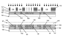
- FIG. 1 shows providing an IC chip 94 including a device layer 100 , i.e., including transistor devices, etc., (not shown).
- IC chip 94 is fabricated up to and including a middle of line (MOL) layer 102 over device layer 100 using any now known or later developed processes.
- MOL layer 102 includes a contact 104 positioned within a high dielectric constant (high-k) dielectric 106 , i.e., any dielectric having k ⁇ 3.9.
- contact 104 may include tungsten (W), copper (Cu) or aluminum (Al).
- Contact 104 may also include any appropriate liner including refractory metals and/or nitrides thereof.
- high-k dielectric 106 may include, for example, a silicon dioxide (SiO 2 ) (e.g., undoped silicon glass (USG)) or borophosphosilicate glass (BPSG)), tetraethyl orthosilicate Si(OC 2 H 5 ) 4 (TEOS).
- SiO 2 silicon dioxide
- BPSG borophosphosilicate glass
- TEOS tetraethyl orthosilicate Si(OC 2 H 5 ) 4
- contact 104 is electrically coupled to parts of devices within device layer 102 , e.g., gates or source/drain regions of transistors.
- FIG. 2 shows recessing high-k dielectric 106 such that contact 104 extends beyond an upper surface 108 of the high-k dielectric.
- the recessing may be achieved, for example, by using dilute hydrofluoric (HF) acid of concentrations of 100:1 to 300:1 in de-ionized water. This process will recess high-k dielectric 106 selectively to contact 104 .
- the amount of the recessing may be selected to prevent overetching during subsequent opening forming ( FIG. 5 ).
- FIG. 3 shows forming a low dielectric constant (low-k) dielectric 120 over high-k dielectric 106 such that low-k dielectric 120 surrounds at least a (upper) portion of contact 104 , i.e., that portion extending beyond high-k dielectric 106 ( FIG. 2 ).
- Low-k dielectric 120 may include, for example, a spin-on polymer, vapor deposited SiLKTM (available from Dow Chemical), vapor deposited hydrogenated silicon oxycarbide (SiCOH), organosilicates or other porous low-k dielectrics.
- low-k dielectric 120 e.g., k ⁇ 3.9
- FIG. 3 also shows forming a planarizing layer 122 , 124 over low-k dielectric 120 so that further photolithography based processing may proceed.
- this process may include forming a non-photoactive polymer layer 122 (e.g., NFCTM available from JSR), and forming a (thin) low temperature oxide (LTO) layer 124 over non-photoactive polymer layer 122 .
- NFCTM non-photoactive polymer layer
- LTO low temperature oxide
- Other single or multiple layer material may also be employed.
- This process may include patterning a mask 132 , first etching ( FIG. 4 ) to open LTO layer 124 and second etching ( FIG. 5 ) planarizing layer 122 , 124 and low-k dielectric 120 at substantially the same rate.
- the first etching FIG. 4
- LTO layer 4 may include a non-selective reactive ion etch (RIE) and can be selective to the underlying non-photoactive polymer layer 122 by the use of hydrogen (H 2 ) and tetrafluoromethane (CF 4 ) type plasma chemistries.
- RIE reactive ion etch
- the selectivity can be as high as or greater than approximately 10:1.
- This process can also use an end-pointed non-selective type of etching using carbon-fluorine (CF x ) based plasmas.
- second etching of planarizing layer 122 , 124 and low-k dielectric 120 is at substantially the same rate for both materials.
- this process may include using a plasma condition that has a selectivity between LTO layer 124 and non-photoactive polymer layer 122 of approximately 1:1 to achieve uniform depth independent of topography.
- This process may include use of a fluorocarbon and oxygen based chemistries such as tetrafluoromethane (CF 4 ) and oxygen (O 2 ).
- This second etching will allow for the formation of the features required in low-k dielectric 120 .
- the second etching is a timed etch to only reach a surface of contact 104 .
- the bottom of opening 130 should be at the surface of contact 104 and a top of low-k dielectric 120 .
- the amount of the initial MOL layer 102 ( FIG. 2 ) high-k dielectric 106 recess ( FIG. 2 ) is determined by the ability of the timed etch ( FIG. 5 ) to finish at the surface of contact 104 , without overetching.
- the depth control of second etching ( FIG. 5 ) can be achieved, for example, with the use of integrated metrology instruments (not shown).
- a metal 140 e.g., copper (Cu) or aluminum (Al)
- This process may include any now known or later developed processes for forming metal 140 within an opening 130 , e.g., performing a cleaning process, forming a liner layer 152 , forming a seed layer (not shown for clarity), depositing a metal and planarizing (e.g., chemical mechanical polishing to remove planarizing layers 122 , 124 , etc.).
- FIG. 6 also shows forming one or more other back-end-of-line (BEOL) layers 142 over metal interconnect 90 using any now known or later developed processing.
- BEOL back-end-of-line
- IC chip 92 including MOL layer 102 including high-k dielectric 106 , a first metal layer 150 above the MOL layer, the first metal layer including low-k dielectric 120 .
- IC chip 92 also includes metal interconnect 90 including contact 104 having a first portion in high-k dielectric 106 of MOL layer 102 and a second portion in low-k dielectric 120 of first metal layer 150 , and a wire (metal 140 ) coupled to contact 104 and positioned in low-k dielectric 120 of first metal layer 150 . As shown in FIG. 6 , low-k dielectric 120 of first metal layer 150 extends beyond a lower surface of liner layer 152 of the wire.
- low-k dielectric 120 are not lost for first metal layer 150 since metal 140 is positioned completely within low-k dielectric 120 rather than entering into high-k dielectric 106 of MOL layer 102 . This allows lowering of the effective dielectric constant with respect to the wire thereby lower the RC (resistance multiplied by capacitance) time delay.
- the methods and structure as described above are used in the fabrication of integrated circuit chips.
- the resulting integrated circuit chips can be distributed by the fabricator in raw wafer form (that is, as a single wafer that has multiple unpackaged chips), as a bare die, or in a packaged form.
- the chip is mounted in a single chip package (such as a plastic carrier, with leads that are affixed to a motherboard or other higher level carrier) or in a multichip package (such as a ceramic carrier that has either or both surface interconnections or buried interconnections).
- the chip is then integrated with other chips, discrete circuit elements, and/or other signal processing devices as part of either (a) an intermediate product, such as a motherboard, or (b) an end product.
- the end product can be any product that includes integrated circuit chips, ranging from toys and other low-end applications to advanced computer products having a display, a keyboard or other input device, and a central processor.
Abstract
Description
Claims (15)
Priority Applications (2)
| Application Number | Priority Date | Filing Date | Title |
|---|---|---|---|
| US11/770,928 US7718525B2 (en) | 2007-06-29 | 2007-06-29 | Metal interconnect forming methods and IC chip including metal interconnect |
| US12/701,045 US7851919B2 (en) | 2007-06-29 | 2010-02-05 | Metal interconnect and IC chip including metal interconnect |
Applications Claiming Priority (1)
| Application Number | Priority Date | Filing Date | Title |
|---|---|---|---|
| US11/770,928 US7718525B2 (en) | 2007-06-29 | 2007-06-29 | Metal interconnect forming methods and IC chip including metal interconnect |
Related Child Applications (1)
| Application Number | Title | Priority Date | Filing Date |
|---|---|---|---|
| US12/701,045 Continuation US7851919B2 (en) | 2007-06-29 | 2010-02-05 | Metal interconnect and IC chip including metal interconnect |
Publications (2)
| Publication Number | Publication Date |
|---|---|
| US20090001592A1 US20090001592A1 (en) | 2009-01-01 |
| US7718525B2 true US7718525B2 (en) | 2010-05-18 |
Family
ID=40159420
Family Applications (2)
| Application Number | Title | Priority Date | Filing Date |
|---|---|---|---|
| US11/770,928 Expired - Fee Related US7718525B2 (en) | 2007-06-29 | 2007-06-29 | Metal interconnect forming methods and IC chip including metal interconnect |
| US12/701,045 Active US7851919B2 (en) | 2007-06-29 | 2010-02-05 | Metal interconnect and IC chip including metal interconnect |
Family Applications After (1)
| Application Number | Title | Priority Date | Filing Date |
|---|---|---|---|
| US12/701,045 Active US7851919B2 (en) | 2007-06-29 | 2010-02-05 | Metal interconnect and IC chip including metal interconnect |
Country Status (1)
| Country | Link |
|---|---|
| US (2) | US7718525B2 (en) |
Cited By (1)
| Publication number | Priority date | Publication date | Assignee | Title |
|---|---|---|---|---|
| US8802569B2 (en) * | 2012-03-13 | 2014-08-12 | Taiwan Semiconductor Manufacturing Company, Ltd. | Method of fabricating a semiconductor device |
Families Citing this family (4)
| Publication number | Priority date | Publication date | Assignee | Title |
|---|---|---|---|---|
| JP2010045533A (en) * | 2008-08-11 | 2010-02-25 | Fujitsu Ltd | Method for manufacturing elastic wave device |
| US8318574B2 (en) | 2010-07-30 | 2012-11-27 | International Business Machines Corporation | SOI trench DRAM structure with backside strap |
| WO2017111868A1 (en) * | 2015-12-23 | 2017-06-29 | Intel Corporation | Approaches for patterning metal line ends for back end of line (beol) interconnects |
| US9947590B1 (en) * | 2016-10-14 | 2018-04-17 | Globalfoundries Inc. | Method, apparatus, and system for using a cover mask for enabling metal line jumping over MOL features in a standard cell |
Citations (9)
| Publication number | Priority date | Publication date | Assignee | Title |
|---|---|---|---|---|
| US5561318A (en) * | 1994-06-07 | 1996-10-01 | Texas Instruments Incorporated | Porous composites as a low dielectric constant material for electronics applications |
| US6278174B1 (en) | 1994-04-28 | 2001-08-21 | Texas Instruments Incorporated | Integrated circuit insulator and structure using low dielectric insulator material including HSQ and fluorinated oxide |
| US6534395B2 (en) | 2000-03-07 | 2003-03-18 | Asm Microchemistry Oy | Method of forming graded thin films using alternating pulses of vapor phase reactants |
| US6642138B2 (en) * | 2001-09-28 | 2003-11-04 | Sharp Laboratories Of America, Inc. | Process of making dual damascene structures using a sacrificial polymer |
| US20050040532A1 (en) * | 2003-08-21 | 2005-02-24 | International Business Machines Corporation | Dual damascene integration of ultra low dielectric constant porous materials |
| US6958524B2 (en) | 2003-11-06 | 2005-10-25 | Taiwan Semiconductor Manufacturing Company, Ltd. | Insulating layer having graded densification |
| US7129164B2 (en) | 2004-10-18 | 2006-10-31 | Taiwan Semiconductor Manufacturing Co., Ltd. | Method for forming a multi-layer low-K dual damascene |
| US7132732B2 (en) | 2003-01-29 | 2006-11-07 | Nec Electronics Corporation | Semiconductor device having two distinct sioch layers |
| US7135398B2 (en) | 2002-11-14 | 2006-11-14 | International Business Machines Corporation | Reliable low-k interconnect structure with hybrid dielectric |
-
2007
- 2007-06-29 US US11/770,928 patent/US7718525B2/en not_active Expired - Fee Related
-
2010
- 2010-02-05 US US12/701,045 patent/US7851919B2/en active Active
Patent Citations (12)
| Publication number | Priority date | Publication date | Assignee | Title |
|---|---|---|---|---|
| US6278174B1 (en) | 1994-04-28 | 2001-08-21 | Texas Instruments Incorporated | Integrated circuit insulator and structure using low dielectric insulator material including HSQ and fluorinated oxide |
| US5561318A (en) * | 1994-06-07 | 1996-10-01 | Texas Instruments Incorporated | Porous composites as a low dielectric constant material for electronics applications |
| US6534395B2 (en) | 2000-03-07 | 2003-03-18 | Asm Microchemistry Oy | Method of forming graded thin films using alternating pulses of vapor phase reactants |
| US6703708B2 (en) | 2000-03-07 | 2004-03-09 | Asm International N.V. | Graded thin films |
| US6933225B2 (en) | 2000-03-07 | 2005-08-23 | Asm International N.V. | Graded thin films |
| US6642138B2 (en) * | 2001-09-28 | 2003-11-04 | Sharp Laboratories Of America, Inc. | Process of making dual damascene structures using a sacrificial polymer |
| US7135398B2 (en) | 2002-11-14 | 2006-11-14 | International Business Machines Corporation | Reliable low-k interconnect structure with hybrid dielectric |
| US7132732B2 (en) | 2003-01-29 | 2006-11-07 | Nec Electronics Corporation | Semiconductor device having two distinct sioch layers |
| US20050040532A1 (en) * | 2003-08-21 | 2005-02-24 | International Business Machines Corporation | Dual damascene integration of ultra low dielectric constant porous materials |
| US7057287B2 (en) * | 2003-08-21 | 2006-06-06 | International Business Machines Corporation | Dual damascene integration of ultra low dielectric constant porous materials |
| US6958524B2 (en) | 2003-11-06 | 2005-10-25 | Taiwan Semiconductor Manufacturing Company, Ltd. | Insulating layer having graded densification |
| US7129164B2 (en) | 2004-10-18 | 2006-10-31 | Taiwan Semiconductor Manufacturing Co., Ltd. | Method for forming a multi-layer low-K dual damascene |
Cited By (1)
| Publication number | Priority date | Publication date | Assignee | Title |
|---|---|---|---|---|
| US8802569B2 (en) * | 2012-03-13 | 2014-08-12 | Taiwan Semiconductor Manufacturing Company, Ltd. | Method of fabricating a semiconductor device |
Also Published As
| Publication number | Publication date |
|---|---|
| US20100133694A1 (en) | 2010-06-03 |
| US7851919B2 (en) | 2010-12-14 |
| US20090001592A1 (en) | 2009-01-01 |
Similar Documents
| Publication | Publication Date | Title |
|---|---|---|
| TWI405301B (en) | Dual wired integrated circuit chips | |
| US10181421B1 (en) | Liner recess for fully aligned via | |
| US10312188B1 (en) | Interconnect structure with method of forming the same | |
| US20070037385A1 (en) | Metal interconnect structure and method | |
| KR20160044990A (en) | Structure and formation method of damascene structure | |
| US11232977B2 (en) | Stepped top via for via resistance reduction | |
| US10832946B1 (en) | Recessed interconnet line having a low-oxygen cap for facilitating a robust planarization process and protecting the interconnect line from downstream etch operations | |
| US7851919B2 (en) | Metal interconnect and IC chip including metal interconnect | |
| JP3696055B2 (en) | Manufacturing method of semiconductor device | |
| US11823998B2 (en) | Top via with next level line selective growth | |
| CN109545735B (en) | Metal internal connection structure and its making method | |
| US20120199980A1 (en) | Integrated circuits having interconnect structures and methods for fabricating integrated circuits having interconnect structures | |
| US6465345B1 (en) | Prevention of inter-channel current leakage in semiconductors | |
| US11139201B2 (en) | Top via with hybrid metallization | |
| US6972251B2 (en) | Method for fabricating copper damascene structures in porous dielectric materials | |
| US20010044202A1 (en) | Method of preventing copper poisoning in the fabrication of metal interconnects | |
| US11127683B2 (en) | Semiconductor structure with substantially straight contact profile | |
| US6277755B1 (en) | Method for fabricating an interconnect | |
| US20150145055A1 (en) | High voltage devices and method of manufacturing the same | |
| US11177166B2 (en) | Etch stop layer removal for capacitance reduction in damascene top via integration | |
| KR100688758B1 (en) | Method for forming gap fill of metal line for semiconductor | |
| US8742587B1 (en) | Metal interconnection structure | |
| US11699650B2 (en) | Integrated circuit structure with capacitor electrodes in different ILD layers, and related methods | |
| US11348867B2 (en) | Capacitor structure for integrated circuit and related methods | |
| US20230170253A1 (en) | Dual-damascene fav interconnects with dielectric plug |
Legal Events
| Date | Code | Title | Description |
|---|---|---|---|
| AS | Assignment |
Owner name: INTERNATIONAL BUSINESS MACHINES CORPORATION, NEW Y Free format text: ASSIGNMENT OF ASSIGNORS INTEREST;ASSIGNORS:BARTH, KARL W.;KEI, RAMONA;KUMAR, KAUSHIK A.;AND OTHERS;REEL/FRAME:019507/0207 Effective date: 20070625 Owner name: INTERNATIONAL BUSINESS MACHINES CORPORATION,NEW YO Free format text: ASSIGNMENT OF ASSIGNORS INTEREST;ASSIGNORS:BARTH, KARL W.;KEI, RAMONA;KUMAR, KAUSHIK A.;AND OTHERS;REEL/FRAME:019507/0207 Effective date: 20070625 |
|
| FEPP | Fee payment procedure |
Free format text: PAYOR NUMBER ASSIGNED (ORIGINAL EVENT CODE: ASPN); ENTITY STATUS OF PATENT OWNER: LARGE ENTITY |
|
| STCF | Information on status: patent grant |
Free format text: PATENTED CASE |
|
| REMI | Maintenance fee reminder mailed | ||
| FPAY | Fee payment |
Year of fee payment: 4 |
|
| SULP | Surcharge for late payment | ||
| AS | Assignment |
Owner name: GLOBALFOUNDRIES U.S. 2 LLC, NEW YORK Free format text: ASSIGNMENT OF ASSIGNORS INTEREST;ASSIGNOR:INTERNATIONAL BUSINESS MACHINES CORPORATION;REEL/FRAME:036550/0001 Effective date: 20150629 |
|
| AS | Assignment |
Owner name: GLOBALFOUNDRIES INC., CAYMAN ISLANDS Free format text: ASSIGNMENT OF ASSIGNORS INTEREST;ASSIGNORS:GLOBALFOUNDRIES U.S. 2 LLC;GLOBALFOUNDRIES U.S. INC.;REEL/FRAME:036779/0001 Effective date: 20150910 |
|
| AS | Assignment |
Owner name: AURIGA INNOVATIONS, INC., CANADA Free format text: ASSIGNMENT OF ASSIGNORS INTEREST;ASSIGNOR:GLOBALFOUNDRIES INC.;REEL/FRAME:041777/0233 Effective date: 20161207 |
|
| MAFP | Maintenance fee payment |
Free format text: PAYMENT OF MAINTENANCE FEE, 8TH YEAR, LARGE ENTITY (ORIGINAL EVENT CODE: M1552) Year of fee payment: 8 |
|
| FEPP | Fee payment procedure |
Free format text: MAINTENANCE FEE REMINDER MAILED (ORIGINAL EVENT CODE: REM.); ENTITY STATUS OF PATENT OWNER: LARGE ENTITY |
|
| LAPS | Lapse for failure to pay maintenance fees |
Free format text: PATENT EXPIRED FOR FAILURE TO PAY MAINTENANCE FEES (ORIGINAL EVENT CODE: EXP.); ENTITY STATUS OF PATENT OWNER: LARGE ENTITY |
|
| STCH | Information on status: patent discontinuation |
Free format text: PATENT EXPIRED DUE TO NONPAYMENT OF MAINTENANCE FEES UNDER 37 CFR 1.362 |
|
| FP | Lapsed due to failure to pay maintenance fee |
Effective date: 20220518 |