US7528432B2 - Semiconductor device having a capacitor and protection insulating films for same - Google Patents
Semiconductor device having a capacitor and protection insulating films for same Download PDFInfo
- Publication number
- US7528432B2 US7528432B2 US10/697,944 US69794403A US7528432B2 US 7528432 B2 US7528432 B2 US 7528432B2 US 69794403 A US69794403 A US 69794403A US 7528432 B2 US7528432 B2 US 7528432B2
- Authority
- US
- United States
- Prior art keywords
- insulating film
- film
- capacitor
- protection insulating
- capacitor protection
- Prior art date
- Legal status (The legal status is an assumption and is not a legal conclusion. Google has not performed a legal analysis and makes no representation as to the accuracy of the status listed.)
- Expired - Fee Related, expires
Links
Images


Classifications
-
- H—ELECTRICITY
- H10—SEMICONDUCTOR DEVICES; ELECTRIC SOLID-STATE DEVICES NOT OTHERWISE PROVIDED FOR
- H10B—ELECTRONIC MEMORY DEVICES
- H10B69/00—Erasable-and-programmable ROM [EPROM] devices not provided for in groups H10B41/00 - H10B63/00, e.g. ultraviolet erasable-and-programmable ROM [UVEPROM] devices
-
- H—ELECTRICITY
- H01—ELECTRIC ELEMENTS
- H01L—SEMICONDUCTOR DEVICES NOT COVERED BY CLASS H10
- H01L21/00—Processes or apparatus adapted for the manufacture or treatment of semiconductor or solid state devices or of parts thereof
- H01L21/02—Manufacture or treatment of semiconductor devices or of parts thereof
- H01L21/02104—Forming layers
- H01L21/02107—Forming insulating materials on a substrate
- H01L21/02109—Forming insulating materials on a substrate characterised by the type of layer, e.g. type of material, porous/non-porous, pre-cursors, mixtures or laminates
- H01L21/02112—Forming insulating materials on a substrate characterised by the type of layer, e.g. type of material, porous/non-porous, pre-cursors, mixtures or laminates characterised by the material of the layer
- H01L21/02123—Forming insulating materials on a substrate characterised by the type of layer, e.g. type of material, porous/non-porous, pre-cursors, mixtures or laminates characterised by the material of the layer the material containing silicon
- H01L21/02126—Forming insulating materials on a substrate characterised by the type of layer, e.g. type of material, porous/non-porous, pre-cursors, mixtures or laminates characterised by the material of the layer the material containing silicon the material containing Si, O, and at least one of H, N, C, F, or other non-metal elements, e.g. SiOC, SiOC:H or SiONC
- H01L21/0214—Forming insulating materials on a substrate characterised by the type of layer, e.g. type of material, porous/non-porous, pre-cursors, mixtures or laminates characterised by the material of the layer the material containing silicon the material containing Si, O, and at least one of H, N, C, F, or other non-metal elements, e.g. SiOC, SiOC:H or SiONC the material being a silicon oxynitride, e.g. SiON or SiON:H
-
- H—ELECTRICITY
- H01—ELECTRIC ELEMENTS
- H01L—SEMICONDUCTOR DEVICES NOT COVERED BY CLASS H10
- H01L21/00—Processes or apparatus adapted for the manufacture or treatment of semiconductor or solid state devices or of parts thereof
- H01L21/02—Manufacture or treatment of semiconductor devices or of parts thereof
- H01L21/02104—Forming layers
- H01L21/02107—Forming insulating materials on a substrate
- H01L21/02109—Forming insulating materials on a substrate characterised by the type of layer, e.g. type of material, porous/non-porous, pre-cursors, mixtures or laminates
- H01L21/02112—Forming insulating materials on a substrate characterised by the type of layer, e.g. type of material, porous/non-porous, pre-cursors, mixtures or laminates characterised by the material of the layer
- H01L21/02123—Forming insulating materials on a substrate characterised by the type of layer, e.g. type of material, porous/non-porous, pre-cursors, mixtures or laminates characterised by the material of the layer the material containing silicon
- H01L21/02164—Forming insulating materials on a substrate characterised by the type of layer, e.g. type of material, porous/non-porous, pre-cursors, mixtures or laminates characterised by the material of the layer the material containing silicon the material being a silicon oxide, e.g. SiO2
-
- H—ELECTRICITY
- H01—ELECTRIC ELEMENTS
- H01L—SEMICONDUCTOR DEVICES NOT COVERED BY CLASS H10
- H01L21/00—Processes or apparatus adapted for the manufacture or treatment of semiconductor or solid state devices or of parts thereof
- H01L21/02—Manufacture or treatment of semiconductor devices or of parts thereof
- H01L21/02104—Forming layers
- H01L21/02107—Forming insulating materials on a substrate
- H01L21/02109—Forming insulating materials on a substrate characterised by the type of layer, e.g. type of material, porous/non-porous, pre-cursors, mixtures or laminates
- H01L21/02112—Forming insulating materials on a substrate characterised by the type of layer, e.g. type of material, porous/non-porous, pre-cursors, mixtures or laminates characterised by the material of the layer
- H01L21/02123—Forming insulating materials on a substrate characterised by the type of layer, e.g. type of material, porous/non-porous, pre-cursors, mixtures or laminates characterised by the material of the layer the material containing silicon
- H01L21/0217—Forming insulating materials on a substrate characterised by the type of layer, e.g. type of material, porous/non-porous, pre-cursors, mixtures or laminates characterised by the material of the layer the material containing silicon the material being a silicon nitride not containing oxygen, e.g. SixNy or SixByNz
-
- H—ELECTRICITY
- H01—ELECTRIC ELEMENTS
- H01L—SEMICONDUCTOR DEVICES NOT COVERED BY CLASS H10
- H01L21/00—Processes or apparatus adapted for the manufacture or treatment of semiconductor or solid state devices or of parts thereof
- H01L21/02—Manufacture or treatment of semiconductor devices or of parts thereof
- H01L21/02104—Forming layers
- H01L21/02107—Forming insulating materials on a substrate
- H01L21/02109—Forming insulating materials on a substrate characterised by the type of layer, e.g. type of material, porous/non-porous, pre-cursors, mixtures or laminates
- H01L21/02112—Forming insulating materials on a substrate characterised by the type of layer, e.g. type of material, porous/non-porous, pre-cursors, mixtures or laminates characterised by the material of the layer
- H01L21/02172—Forming insulating materials on a substrate characterised by the type of layer, e.g. type of material, porous/non-porous, pre-cursors, mixtures or laminates characterised by the material of the layer the material containing at least one metal element, e.g. metal oxides, metal nitrides, metal oxynitrides or metal carbides
- H01L21/02175—Forming insulating materials on a substrate characterised by the type of layer, e.g. type of material, porous/non-porous, pre-cursors, mixtures or laminates characterised by the material of the layer the material containing at least one metal element, e.g. metal oxides, metal nitrides, metal oxynitrides or metal carbides characterised by the metal
- H01L21/02178—Forming insulating materials on a substrate characterised by the type of layer, e.g. type of material, porous/non-porous, pre-cursors, mixtures or laminates characterised by the material of the layer the material containing at least one metal element, e.g. metal oxides, metal nitrides, metal oxynitrides or metal carbides characterised by the metal the material containing aluminium, e.g. Al2O3
-
- H—ELECTRICITY
- H01—ELECTRIC ELEMENTS
- H01L—SEMICONDUCTOR DEVICES NOT COVERED BY CLASS H10
- H01L21/00—Processes or apparatus adapted for the manufacture or treatment of semiconductor or solid state devices or of parts thereof
- H01L21/02—Manufacture or treatment of semiconductor devices or of parts thereof
- H01L21/02104—Forming layers
- H01L21/02107—Forming insulating materials on a substrate
- H01L21/02109—Forming insulating materials on a substrate characterised by the type of layer, e.g. type of material, porous/non-porous, pre-cursors, mixtures or laminates
- H01L21/02112—Forming insulating materials on a substrate characterised by the type of layer, e.g. type of material, porous/non-porous, pre-cursors, mixtures or laminates characterised by the material of the layer
- H01L21/02172—Forming insulating materials on a substrate characterised by the type of layer, e.g. type of material, porous/non-porous, pre-cursors, mixtures or laminates characterised by the material of the layer the material containing at least one metal element, e.g. metal oxides, metal nitrides, metal oxynitrides or metal carbides
- H01L21/02175—Forming insulating materials on a substrate characterised by the type of layer, e.g. type of material, porous/non-porous, pre-cursors, mixtures or laminates characterised by the material of the layer the material containing at least one metal element, e.g. metal oxides, metal nitrides, metal oxynitrides or metal carbides characterised by the metal
- H01L21/02186—Forming insulating materials on a substrate characterised by the type of layer, e.g. type of material, porous/non-porous, pre-cursors, mixtures or laminates characterised by the material of the layer the material containing at least one metal element, e.g. metal oxides, metal nitrides, metal oxynitrides or metal carbides characterised by the metal the material containing titanium, e.g. TiO2
-
- H—ELECTRICITY
- H01—ELECTRIC ELEMENTS
- H01L—SEMICONDUCTOR DEVICES NOT COVERED BY CLASS H10
- H01L21/00—Processes or apparatus adapted for the manufacture or treatment of semiconductor or solid state devices or of parts thereof
- H01L21/02—Manufacture or treatment of semiconductor devices or of parts thereof
- H01L21/02104—Forming layers
- H01L21/02107—Forming insulating materials on a substrate
- H01L21/02109—Forming insulating materials on a substrate characterised by the type of layer, e.g. type of material, porous/non-porous, pre-cursors, mixtures or laminates
- H01L21/02112—Forming insulating materials on a substrate characterised by the type of layer, e.g. type of material, porous/non-porous, pre-cursors, mixtures or laminates characterised by the material of the layer
- H01L21/02172—Forming insulating materials on a substrate characterised by the type of layer, e.g. type of material, porous/non-porous, pre-cursors, mixtures or laminates characterised by the material of the layer the material containing at least one metal element, e.g. metal oxides, metal nitrides, metal oxynitrides or metal carbides
- H01L21/02197—Forming insulating materials on a substrate characterised by the type of layer, e.g. type of material, porous/non-porous, pre-cursors, mixtures or laminates characterised by the material of the layer the material containing at least one metal element, e.g. metal oxides, metal nitrides, metal oxynitrides or metal carbides the material having a perovskite structure, e.g. BaTiO3
-
- H—ELECTRICITY
- H01—ELECTRIC ELEMENTS
- H01L—SEMICONDUCTOR DEVICES NOT COVERED BY CLASS H10
- H01L21/00—Processes or apparatus adapted for the manufacture or treatment of semiconductor or solid state devices or of parts thereof
- H01L21/02—Manufacture or treatment of semiconductor devices or of parts thereof
- H01L21/02104—Forming layers
- H01L21/02107—Forming insulating materials on a substrate
- H01L21/02109—Forming insulating materials on a substrate characterised by the type of layer, e.g. type of material, porous/non-porous, pre-cursors, mixtures or laminates
- H01L21/022—Forming insulating materials on a substrate characterised by the type of layer, e.g. type of material, porous/non-porous, pre-cursors, mixtures or laminates the layer being a laminate, i.e. composed of sublayers, e.g. stacks of alternating high-k metal oxides
-
- H—ELECTRICITY
- H01—ELECTRIC ELEMENTS
- H01L—SEMICONDUCTOR DEVICES NOT COVERED BY CLASS H10
- H01L21/00—Processes or apparatus adapted for the manufacture or treatment of semiconductor or solid state devices or of parts thereof
- H01L21/02—Manufacture or treatment of semiconductor devices or of parts thereof
- H01L21/02104—Forming layers
- H01L21/02107—Forming insulating materials on a substrate
- H01L21/02109—Forming insulating materials on a substrate characterised by the type of layer, e.g. type of material, porous/non-porous, pre-cursors, mixtures or laminates
- H01L21/02205—Forming insulating materials on a substrate characterised by the type of layer, e.g. type of material, porous/non-porous, pre-cursors, mixtures or laminates the layer being characterised by the precursor material for deposition
- H01L21/02208—Forming insulating materials on a substrate characterised by the type of layer, e.g. type of material, porous/non-porous, pre-cursors, mixtures or laminates the layer being characterised by the precursor material for deposition the precursor containing a compound comprising Si
- H01L21/02211—Forming insulating materials on a substrate characterised by the type of layer, e.g. type of material, porous/non-porous, pre-cursors, mixtures or laminates the layer being characterised by the precursor material for deposition the precursor containing a compound comprising Si the compound being a silane, e.g. disilane, methylsilane or chlorosilane
-
- H—ELECTRICITY
- H01—ELECTRIC ELEMENTS
- H01L—SEMICONDUCTOR DEVICES NOT COVERED BY CLASS H10
- H01L21/00—Processes or apparatus adapted for the manufacture or treatment of semiconductor or solid state devices or of parts thereof
- H01L21/02—Manufacture or treatment of semiconductor devices or of parts thereof
- H01L21/02104—Forming layers
- H01L21/02107—Forming insulating materials on a substrate
- H01L21/02225—Forming insulating materials on a substrate characterised by the process for the formation of the insulating layer
- H01L21/0226—Forming insulating materials on a substrate characterised by the process for the formation of the insulating layer formation by a deposition process
- H01L21/02263—Forming insulating materials on a substrate characterised by the process for the formation of the insulating layer formation by a deposition process deposition from the gas or vapour phase
- H01L21/02271—Forming insulating materials on a substrate characterised by the process for the formation of the insulating layer formation by a deposition process deposition from the gas or vapour phase deposition by decomposition or reaction of gaseous or vapour phase compounds, i.e. chemical vapour deposition
- H01L21/02274—Forming insulating materials on a substrate characterised by the process for the formation of the insulating layer formation by a deposition process deposition from the gas or vapour phase deposition by decomposition or reaction of gaseous or vapour phase compounds, i.e. chemical vapour deposition in the presence of a plasma [PECVD]
-
- H—ELECTRICITY
- H01—ELECTRIC ELEMENTS
- H01L—SEMICONDUCTOR DEVICES NOT COVERED BY CLASS H10
- H01L21/00—Processes or apparatus adapted for the manufacture or treatment of semiconductor or solid state devices or of parts thereof
- H01L21/02—Manufacture or treatment of semiconductor devices or of parts thereof
- H01L21/02104—Forming layers
- H01L21/02107—Forming insulating materials on a substrate
- H01L21/02296—Forming insulating materials on a substrate characterised by the treatment performed before or after the formation of the layer
- H01L21/02318—Forming insulating materials on a substrate characterised by the treatment performed before or after the formation of the layer post-treatment
- H01L21/02337—Forming insulating materials on a substrate characterised by the treatment performed before or after the formation of the layer post-treatment treatment by exposure to a gas or vapour
- H01L21/0234—Forming insulating materials on a substrate characterised by the treatment performed before or after the formation of the layer post-treatment treatment by exposure to a gas or vapour treatment by exposure to a plasma
-
- H—ELECTRICITY
- H01—ELECTRIC ELEMENTS
- H01L—SEMICONDUCTOR DEVICES NOT COVERED BY CLASS H10
- H01L21/00—Processes or apparatus adapted for the manufacture or treatment of semiconductor or solid state devices or of parts thereof
- H01L21/02—Manufacture or treatment of semiconductor devices or of parts thereof
- H01L21/02104—Forming layers
- H01L21/02107—Forming insulating materials on a substrate
- H01L21/02296—Forming insulating materials on a substrate characterised by the treatment performed before or after the formation of the layer
- H01L21/02318—Forming insulating materials on a substrate characterised by the treatment performed before or after the formation of the layer post-treatment
- H01L21/02356—Forming insulating materials on a substrate characterised by the treatment performed before or after the formation of the layer post-treatment treatment to change the morphology of the insulating layer, e.g. transformation of an amorphous layer into a crystalline layer
-
- H—ELECTRICITY
- H01—ELECTRIC ELEMENTS
- H01L—SEMICONDUCTOR DEVICES NOT COVERED BY CLASS H10
- H01L27/00—Devices consisting of a plurality of semiconductor or other solid-state components formed in or on a common substrate
- H01L27/02—Devices consisting of a plurality of semiconductor or other solid-state components formed in or on a common substrate including semiconductor components specially adapted for rectifying, oscillating, amplifying or switching and having at least one potential-jump barrier or surface barrier; including integrated passive circuit elements with at least one potential-jump barrier or surface barrier
- H01L27/04—Devices consisting of a plurality of semiconductor or other solid-state components formed in or on a common substrate including semiconductor components specially adapted for rectifying, oscillating, amplifying or switching and having at least one potential-jump barrier or surface barrier; including integrated passive circuit elements with at least one potential-jump barrier or surface barrier the substrate being a semiconductor body
- H01L27/06—Devices consisting of a plurality of semiconductor or other solid-state components formed in or on a common substrate including semiconductor components specially adapted for rectifying, oscillating, amplifying or switching and having at least one potential-jump barrier or surface barrier; including integrated passive circuit elements with at least one potential-jump barrier or surface barrier the substrate being a semiconductor body including a plurality of individual components in a non-repetitive configuration
- H01L27/0611—Devices consisting of a plurality of semiconductor or other solid-state components formed in or on a common substrate including semiconductor components specially adapted for rectifying, oscillating, amplifying or switching and having at least one potential-jump barrier or surface barrier; including integrated passive circuit elements with at least one potential-jump barrier or surface barrier the substrate being a semiconductor body including a plurality of individual components in a non-repetitive configuration integrated circuits having a two-dimensional layout of components without a common active region
- H01L27/0617—Devices consisting of a plurality of semiconductor or other solid-state components formed in or on a common substrate including semiconductor components specially adapted for rectifying, oscillating, amplifying or switching and having at least one potential-jump barrier or surface barrier; including integrated passive circuit elements with at least one potential-jump barrier or surface barrier the substrate being a semiconductor body including a plurality of individual components in a non-repetitive configuration integrated circuits having a two-dimensional layout of components without a common active region comprising components of the field-effect type
- H01L27/0629—Devices consisting of a plurality of semiconductor or other solid-state components formed in or on a common substrate including semiconductor components specially adapted for rectifying, oscillating, amplifying or switching and having at least one potential-jump barrier or surface barrier; including integrated passive circuit elements with at least one potential-jump barrier or surface barrier the substrate being a semiconductor body including a plurality of individual components in a non-repetitive configuration integrated circuits having a two-dimensional layout of components without a common active region comprising components of the field-effect type in combination with diodes, or resistors, or capacitors
-
- H—ELECTRICITY
- H01—ELECTRIC ELEMENTS
- H01L—SEMICONDUCTOR DEVICES NOT COVERED BY CLASS H10
- H01L28/00—Passive two-terminal components without a potential-jump or surface barrier for integrated circuits; Details thereof; Multistep manufacturing processes therefor
- H01L28/40—Capacitors
- H01L28/55—Capacitors with a dielectric comprising a perovskite structure material
- H01L28/57—Capacitors with a dielectric comprising a perovskite structure material comprising a barrier layer to prevent diffusion of hydrogen or oxygen
-
- H—ELECTRICITY
- H10—SEMICONDUCTOR DEVICES; ELECTRIC SOLID-STATE DEVICES NOT OTHERWISE PROVIDED FOR
- H10B—ELECTRONIC MEMORY DEVICES
- H10B53/00—Ferroelectric RAM [FeRAM] devices comprising ferroelectric memory capacitors
-
- H—ELECTRICITY
- H10—SEMICONDUCTOR DEVICES; ELECTRIC SOLID-STATE DEVICES NOT OTHERWISE PROVIDED FOR
- H10B—ELECTRONIC MEMORY DEVICES
- H10B53/00—Ferroelectric RAM [FeRAM] devices comprising ferroelectric memory capacitors
- H10B53/30—Ferroelectric RAM [FeRAM] devices comprising ferroelectric memory capacitors characterised by the memory core region
-
- H—ELECTRICITY
- H01—ELECTRIC ELEMENTS
- H01L—SEMICONDUCTOR DEVICES NOT COVERED BY CLASS H10
- H01L21/00—Processes or apparatus adapted for the manufacture or treatment of semiconductor or solid state devices or of parts thereof
- H01L21/02—Manufacture or treatment of semiconductor devices or of parts thereof
- H01L21/04—Manufacture or treatment of semiconductor devices or of parts thereof the devices having at least one potential-jump barrier or surface barrier, e.g. PN junction, depletion layer or carrier concentration layer
- H01L21/18—Manufacture or treatment of semiconductor devices or of parts thereof the devices having at least one potential-jump barrier or surface barrier, e.g. PN junction, depletion layer or carrier concentration layer the devices having semiconductor bodies comprising elements of Group IV of the Periodic System or AIIIBV compounds with or without impurities, e.g. doping materials
- H01L21/30—Treatment of semiconductor bodies using processes or apparatus not provided for in groups H01L21/20 - H01L21/26
- H01L21/31—Treatment of semiconductor bodies using processes or apparatus not provided for in groups H01L21/20 - H01L21/26 to form insulating layers thereon, e.g. for masking or by using photolithographic techniques; After treatment of these layers; Selection of materials for these layers
- H01L21/314—Inorganic layers
- H01L21/316—Inorganic layers composed of oxides or glassy oxides or oxide based glass
- H01L21/31604—Deposition from a gas or vapour
- H01L21/31608—Deposition of SiO2
- H01L21/31612—Deposition of SiO2 on a silicon body
-
- H—ELECTRICITY
- H01—ELECTRIC ELEMENTS
- H01L—SEMICONDUCTOR DEVICES NOT COVERED BY CLASS H10
- H01L21/00—Processes or apparatus adapted for the manufacture or treatment of semiconductor or solid state devices or of parts thereof
- H01L21/02—Manufacture or treatment of semiconductor devices or of parts thereof
- H01L21/04—Manufacture or treatment of semiconductor devices or of parts thereof the devices having at least one potential-jump barrier or surface barrier, e.g. PN junction, depletion layer or carrier concentration layer
- H01L21/18—Manufacture or treatment of semiconductor devices or of parts thereof the devices having at least one potential-jump barrier or surface barrier, e.g. PN junction, depletion layer or carrier concentration layer the devices having semiconductor bodies comprising elements of Group IV of the Periodic System or AIIIBV compounds with or without impurities, e.g. doping materials
- H01L21/30—Treatment of semiconductor bodies using processes or apparatus not provided for in groups H01L21/20 - H01L21/26
- H01L21/31—Treatment of semiconductor bodies using processes or apparatus not provided for in groups H01L21/20 - H01L21/26 to form insulating layers thereon, e.g. for masking or by using photolithographic techniques; After treatment of these layers; Selection of materials for these layers
- H01L21/314—Inorganic layers
- H01L21/316—Inorganic layers composed of oxides or glassy oxides or oxide based glass
- H01L21/31604—Deposition from a gas or vapour
- H01L21/31616—Deposition of Al2O3
- H01L21/3162—Deposition of Al2O3 on a silicon body
Definitions
- the present invention relates to a semiconductor device and a method of manufacturing the same and, more particularly, to a semiconductor device having a nonvolatile memory (FeRAM: Ferroelectric Random Access Memory) in which ferroelectric material is employed as the dielectric film of the capacitor and a method of manufacturing the same.
- FeRAM Ferroelectric Random Access Memory
- the cell area will be more reduced in response to the demand for the higher integration in the future. If the cell area is reduced in such a way, the interval between neighboring capacitors is also shortened and the wiring interval is also narrowed accordingly. It is general that the spaces between the capacitors and the spaces between the wirings are buried with the insulating film. In this case, if the higher integration makes progress as above, the insulating film having the good filling property not to form the cavity (also called as the blowhole or the void) between the capacitors must be employed as such insulating film.
- the film that is formed by the high density plasma CVD (HDPCVD) method is known in the prior art.
- the insulating film that is formed by the HDPCVD method can be shown in FIG. 1 of Patent Application Publication (KOKAI) 2001-210798, for example.
- KKAI Patent Application Publication
- the HDP oxide can be used as the insulating film 134 for covering the capacitor in FIG. 1.
- SiH 4 is used in general as the film forming gas in the HDPCVD method. This SiH 4 is decomposed during the film formation to generate the hydrogen. Thus, there is given the chance that the ferroelectric film of the capacitor is exposed to the hydrogen.
- the structure for covering the capacitor with the insulating film made of the metal oxide, e.g., the alumina (Al 2 O 3 ) film is known.
- the metal oxide e.g., the alumina (Al 2 O 3 ) film.
- Such structure is disclosed in Patent Application Hei 11-215600, Patent Application Publication (KOKAI) 2001-44375, Patent Application Publication (KOKAI) Hei 6-29098, and Japanese Patent No. 3056973.
- a semiconductor device manufacturing method which comprises the steps of forming a first insulating film over a semiconductor substrate; forming a first conductive film, a ferroelectric film, and a second conductive film sequentially on the first insulating film; forming an upper electrode of a capacitor by patterning the second conductive film; forming a dielectric film of the capacitor by patterning the ferroelectric film; forming a lower electrode of the capacitor by patterning the first conductive film; forming a first capacitor protection insulating film covering the dielectric film and the upper electrode; forming a second capacitor protection insulating film, which covers the first capacitor protection insulating film, by a chemical vapor deposition method in a state that a bias voltage is not applied to the semiconductor substrate; and forming a second insulating film on the second capacitor protection insulating film by the chemical vapor deposition method in a state that the bias voltage is applied to the semiconductor substrate.
- the collision energy of the sputter ions and other ions is absorbed by the second capacitor protection insulating film to decrease its moving speed.
- the ions can be blocked by the underlying first capacitor protection insulating film, and thus the capacitor dielectric film can be prevented from being deteriorated by the ions.
- the second capacitor protection insulating film is formed in the state that the bias voltage is not applied to the semiconductor substrate. Therefore, the capacitor dielectric film can be prevented from being deteriorated in the film formation.
- the deterioration of the capacitor dielectric film in the film formation can be prevented.
- the second capacitor protection insulating film is formed by the chemical vapor deposition method using the reaction gas containing TEOS, the coverage of the second capacitor protection insulating film can be improved, and thus the collision ions can be absorbed at the upper portion and the side portions of the capacitor uniformly. Further, since hydrogen, which is reducing substance, is hard to generate from TEOS in contrast to SiH 4 , there is no chance that the capacitor is deteriorated by the hydrogen.
- the above first capacitor protection insulating film be formed to have a double-layered structure consisting of the lower protection insulating film, which covers the dielectric film and the upper electrode of the capacitor, and the upper protection insulating film, which is formed on the lower protection insulating film and the first insulating film. According to this, since the capacitor and the first insulating film are covered continuously with the upper protection insulating film, it is possible to prevent the entering of the reducing substance such as the hydrogen, or the like into the capacitor dielectric film via the first insulating film.
- the capacitor is formed in plural, if the total film thickness of the first capacitor protection insulating film and the second capacitor protection insulating film is set smaller than half of the minimum interval among a plurality of upper electrodes, the spaces between the capacitors can be filled desirably, with the second insulating film between the capacitors free from cavity.
- the film thickness of the second insulating film be set thicker than the total film thickness of the capacitor upper electrode, the capacitor dielectric film, and the capacitor lower electrode but thinner than the film thickness that is obtained by adding 1 ⁇ m to the total film thickness. According to this, while suppressing maximally the deterioration of the capacitor dielectric film due to ions that are generated in the film formation of the second insulating film, the spaces between the capacitors can be filled with the second insulating film.
- the third insulating film is formed on the second insulating film before the polishing, and then the second and third insulating films are polished together. Therefore, the film thickness to be polished can be increased and also the distribution of the film thickness after the polishing can be set uniformly.
- FIGS. 1A to 1R are sectional views showing steps of manufacturing an FeRAM as a semiconductor device according to a first embodiment of the present invention
- FIG. 2 is a plan view showing the semiconductor device, shown in FIG. 1C , according to the first embodiment of the present invention
- FIG. 3 is a plan view showing the semiconductor device, shown in FIG. 1D , according to the first embodiment of the present invention
- FIG. 4 is a plan view showing the semiconductor device, shown in FIG. 1F , according to the first embodiment of the present invention.
- FIG. 5 is a plan view showing the semiconductor device, shown in FIG. 1L , according to the first embodiment of the present invention.
- FIG. 6 is a plan view showing the semiconductor device, shown in FIG. 1P , according to the first embodiment of the present invention.
- FIG. 7 is a plan view showing the semiconductor device, shown in FIG. 1R , according to the first embodiment of the present invention.
- FIG. 8 is a configurative view showing the plasma CVD equipment employed in the steps of manufacturing the semiconductor device according to respective embodiments of the present invention.
- FIG. 9 is a configurative view showing the HDPCVD equipment employed in the steps of manufacturing the semiconductor device according to respective embodiments of the present invention.
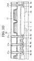
- FIGS. 10A and 10B are sectional views for explaining the conditions that are satisfied by a thickness of a second capacitor protection insulating film in the steps of manufacturing the semiconductor device according to respective embodiments of the present invention
- FIG. 11 is a graph showing differences in the damage of the capacitor Q between the case where the second interlayer insulating film is formed while applying the bias voltage and the case where the second interlayer insulating film is formed while not applying the bias voltage, during the steps of manufacturing the semiconductor device according to the first embodiment of the present invention;
- FIG. 12 is a graph showing differences in the damage of the capacitor Q between the case where the second capacitor protection insulating film is formed and the case where the second capacitor protection insulating film is not formed, during the steps of manufacturing the semiconductor device according to the first embodiment of the present invention
- FIGS. 13A to 13N are sectional views showing steps of manufacturing an FeRAM as a semiconductor device according to a second embodiment of the present invention.
- FIG. 14 is a plan view showing the semiconductor device, shown in FIG. 13N , according to the second embodiment of the present invention.
- FIG. 15 is a sectional view showing the semiconductor device, taken along a II-II line in FIG. 14 .
- FIGS. 1A to 1R are sectional views showing a method of manufacturing an FeRAM as a semiconductor device according to a first embodiment of the present invention in order of the step.
- a device isolating insulating film 2 is formed on a surface of an n-type or p-type silicon (semiconductor) substrate 1 by the LOCOS (Local Oxidation of Silicon) method.
- the LOCOS Local Oxidation of Silicon
- the STI Shallow Trench Isolation
- a p-well 3 a and an n-well 3 b are formed by selectively introducing the p-type impurity and the n-type impurity into a predetermined active region (transistor forming region) of the silicon substrate 1 .
- a silicon oxide film is formed as a gate insulating film 5 by thermally oxidizing a surface of the active region of the silicon substrate 1 .
- an amorphous silicon film or a polysilicon film is formed on overall upper surface of the silicon substrate 1 .
- the resistance of the silicon film is lowered by ion-implanting the n-type impurity and the p-type impurity into the silicon film on the p-well 3 a and the n-well 3 b respectively.
- gate electrodes 6 a , 6 b are formed by patterning the silicon film into a predetermined shape by virtue of the photolithography method.
- the gate electrodes 6 a , 6 b are arranged each other in almost parallel, and constitute a part of the word line WL.
- n-type impurity diffusion regions 4 a serving as the source/drain of the n-channel MOS transistors are formed by ion-implanting the n-type impurity into the p-well 3 a on both sides of the gate electrodes 6 a , 6 b .
- p-type impurity diffusion regions 4 b serving as the source/drain of the p-channel MOS transistors (not shown) are formed by ion-implanting the p-type impurity into the n-well 3 b.
- an insulating film is formed on the overall surface of the silicon substrate 1 . Then, the insulating film is left as a sidewall insulating film 10 only on both side portions of the gate electrodes 6 a , 6 b by etching back the insulating film.
- a silicon oxide (SiO 2 ) film is formed by the CVD (Chemical Vapor Deposition) method.
- the n-type impurity diffusion regions 4 a are made into the LDD (Lightly Doped Drain) structure by implanting the n-type impurity into the p-well 3 a again while using the gate electrodes 6 a , 6 b and the sidewall insulating films 10 as a mask. Also, the p-type impurity diffusion regions 4 b are made into the LDD structure by implanting the p-type impurity into the n-well 3 b again.
- LDD Lightly Doped Drain
- the individual implantation of the n-type impurity and the p-type impurity is carried out using the resist patterns (not shown).
- the n-MOSFET is constructed by the p-well 3 a , the gate electrodes 6 a , 6 b , the n-type impurity diffusion regions 4 a on both sides of the gate electrodes 6 a , 6 b , etc.
- the p-MOSFET (not shown) is constructed by the n-well 3 b , the p-type impurity diffusion regions 4 b , and the gate electrodes (not shown), etc.
- a refractory metal film e.g., a film made of Ti (titanium), Co (cobalt), or the like, is formed on the overall surface.
- refractory metal silicide layers 8 a , 8 b are formed on surfaces of the n-type impurity diffusion regions 4 a and the p-type impurity diffusion regions 4 b respectively by heating this refractory metal film. Then, the unreacted refractory metal film is removed by the wet etching.
- a silicon oxide nitride (SiON) film of about 200 nm thickness is formed as a cover insulating film 7 on the overall surface of the silicon substrate 1 by the plasma CVD method.
- a silicon oxide (SiO 2 ) film of about 1.0 ⁇ m thickness is grown as a first interlayer insulating film (first insulating film) 9 on the cover insulating film 7 by the plasma CVD method using TEOS (tetraethoxy silane) gas.
- a surface of the first interlayer insulating film 9 is planarized by polishing the surface by virtue of the CMP (Chemical Mechanical Polishing) method.
- a titanium (Ti) film and a platinum (Pt) film are formed sequentially on the first interlayer insulating film 9 by the DC sputtering method, and these films constitute a first conductive film 11 .
- a thickness of the Ti film is set to about 10 to 30 nm, e.g., 20 nm
- a thickness of the Pt film is set to about 100 to 300 nm, e.g., 175 nm.
- This Ti film play the role to improve the adhesiveness between the Pt film and the first interlayer insulating film 9 and the role to improve the crystallinity of the Pt film.
- the first conductive film 11 a film made of iridium, ruthenium, ruthenium oxide, strontium ruthenium oxide (SrRuO 3 ), or the like may be formed.
- a PZT (Pb(Zr 1-x Ti x )O 3 ) film having a thickness of 100 to 300 nm, e.g., 240 nm is formed on the first conductive film 11 by the sputtering method, and this film is used as a ferroelectric film 12 .
- the silicon substrate 1 is put in the oxygen atmosphere.
- the crystallizing process of the PZT film constituting the ferroelectric film 12 is carried out by applying the RTA (Rapid Thermal Annealing) process to this PZT film at the temperature of 725° C. for 20 second at a temperature-increasing rate of 125° C./sec, for example.
- RTA Rapid Thermal Annealing
- the method of forming the ferroelectric film 12 there are the spin-on method, the sol-gel method, the MOD (Metal Organic Deposition) method, the MOCVD method.
- the material constituting the ferroelectric film 12 other than PZT, there are the PZT material such as PLZT (Lead Lanthanum Zirconate Titanate: (Pb 1-3x/2 La x )(Zr 1-y Ti y )O 3 ) obtained by adding lanthanum (La) into PZT, PLCSZT obtained by adding lanthanum (La), calcium (Ca), and strontium (Sr) into PZT, etc., and the bismuth (Bi) material such as SrBi 2 (Ta x Nb 1-x ) 2 O 9 (where 0 ⁇ x ⁇ 1), Bi 4 Ti 2 O 12 , etc.
- PLZT Lead Lanthanum Zirconate Titanate: (Pb 1-3x/2 La x )(Zr 1-y Ti y
- an iridium oxide (IrO x ) film is formed as a second conductive film 13 on the ferroelectric film 12 by the sputtering method to a thickness of 100 to 300 nm, e.g., 200 nm.
- a platinum (Pt) film or a strontium ruthenium oxide (SRO) film may be formed by the sputtering method.
- resist patterns (not shown), each having a capacitor upper electrode shape, are formed on the second conductive film 13 , and then the second conductive film 13 is patterned by using the resist patterns as an etching mask. Then, the remaining second conductive film 13 is used as capacitor upper electrodes 13 a.
- the ferroelectric film 12 is annealed in the oxygen atmosphere at the temperature of 650° C. for 60 second. This annealing is carried out to recover the damage which the ferroelectric film 12 received during the sputtering and the etching.
- FIG. 1C a plan view of this FIG. 1C is given as shown in FIG. 2 , and FIG. 1C corresponds to a sectional view taken along a I-I line in FIG. 2 .
- resist patterns (not shown) are formed on the capacitor upper electrodes 13 a , and then the ferroelectric film 12 is patterned by using the resist patterns as an etching mask. Then, the remaining ferroelectric film 12 is used as capacitor dielectric films 12 a . Then, after removing the resist patterns, the capacitor dielectric films 12 a are annealed in the oxygen atmosphere at the temperature of 650° C. for 60 second.
- FIG. 1D a plan view of this FIG. 1D is given as shown in FIG. 3 , and FIG. 1D corresponds to a sectional view taken along a I-I line in FIG. 3 .
- an alumina (Al 2 O 3 ) film of 50 nm thickness is formed as a lower protection insulating film 14 a , which covers the capacitor dielectric films 12 a and the capacitor upper electrodes 13 a , at the ambient temperature by the sputtering method.
- This lower protection insulating film 14 a is formed to protect the capacitor dielectric films 12 a , which are ready to be reduced, from the reducing substance such as the hydrogen and to block the entering of the hydrogen into the inside of the capacitor dielectric films 12 a.
- the bias voltage should not be applied to the silicon substrate 1 in forming this lower protection insulating film 14 a .
- the bias voltage because the bias voltage is not applied, the above disadvantage is not caused.
- a PLZT film, a PZT film, a titanium oxide film, an aluminum nitride film, a silicon nitride film, or a silicon nitride oxide film may be formed.
- the film quality of the capacitor dielectric films 12 a under the lower protection insulating film 14 a is improved by applying the RTA process in the oxygen atmosphere at the temperature of 700° C. for 60 second with the temperature-increasing rate of 125° C./sec.
- the resist (not shown) is coated on the lower protection insulating film 14 a .
- the resist is exposed/developed to be left such that the resist covers the capacitor upper electrodes 13 a and the capacitor dielectric films 12 a .
- the lower protection insulating film 14 a and the first conductive film 11 are patterned by using the resist as an etching mask.
- the lower protection insulating film 14 a is left on the capacitor upper electrodes 13 a and the capacitor dielectric films 12 a .
- the first conductive film 11 left after this patterning is used as capacitor lower electrodes 11 a .
- the etching of the lower protection insulating film 14 a and the first conductive film 11 is carried out by the dry etching using the chlorine as the etching gas.
- capacitors Q each of which is formed by laminating the lower electrode 11 a , the capacitor ferroelectric film 12 a , and the upper electrode 13 a sequentially are formed on the first interlayer insulating film 9 .
- FIG. 1F a plan view of this FIG. 1F is given as shown in FIG. 4 , and FIG. 1F corresponds to a sectional view taken along a I-I line in FIG. 4 . Note that the lower protection insulating film 14 a is omitted in FIG. 4 .
- an alumina (Al 2 O 3 ) film of 20 nm thickness is formed as an upper protection insulating film 14 b on the first interlayer insulating film 9 and the lower protection insulating films 14 a at the ambient temperature by the sputtering method.
- This upper protection insulating film 14 b along with the lower protection insulating film 14 a , constitutes a first capacitor protection insulating film 14 .
- Employing such a double-layered structure for the insulating film 14 increases its film thickness, making it more difficult for the hydrogen to enter into the capacitor ferroelectric film 12 a .
- the upper protection insulating film 14 b covers the capacitors Q and the first interlayer insulating film 9 continuously, the reducing substance such as the hydrogen or the like can be prevented from entering into the capacitors Q from the outside via the first interlayer insulating film 9 .
- the bias voltage is not applied to the silicon substrate 1 in forming the upper protection insulating film 14 b , the deterioration of the capacitor ferroelectric film 12 a by the target atoms can be prevented.
- the silicon substrate 1 is loaded in a chamber 50 of the plasma CVD equipment shown in FIG. 8 .
- a substrate loading table 51 on which the silicon substrate 1 is loaded is grounded, while a gas distributing plate 53 is connected to a high-frequency power supply 54 and the high-frequency power is applied to the gas distributing plate 53 .
- a silicon oxide (SiO 2 ) film of 100 nm thickness is formed as a second capacitor protection insulating film 16 on the first capacitor protection insulating film 14 .
- the bias voltage is not applied to the silicon substrate 1 . Therefore, the plasmanized reaction gas is never pulled into the silicon substrate 1 by the bias voltage, so that there is no possibility that the capacitor ferroelectric film 12 a is deteriorated by the reaction gas.
- the moisture contained in the surface and inside of the second capacitor protection insulating film 16 is discharged to the outside by heating this insulating film 16 in the vacuum chamber (not shown) at the temperature of 350° C.
- the second capacitor protection insulating film 16 is exposed to the N 2 O plasma to extract the moisture and improve the film quality. As a result, the deterioration of the capacitors caused by the heat and the moisture in the subsequent steps can be prevented.
- Such dehydrating process and the plasma process may be executed in the same chamber.
- a supporting electrode on which the silicon substrate 1 is loaded and an opposing electrode that opposes to the supporting electrode are arranged, and the high-frequency power supply can be connected to the opposing electrode.
- the N 2 O gas being introduced into the chamber, first the dehydrating process of the insulating film is executed under the condition that the high-frequency power is not applied to the opposing electrode, and then the N 2 O plasma process of the insulating film is executed by generating the N 2 O plasma between the electrodes under the condition that the high-frequency power is applied to the opposing electrode.
- the frequency of the high-frequency power supply is 13.56 MHz and the power of the high-frequency power supply is 300 W.
- the N 2 O flow rate is 700 sccm.
- the N 2 O plasma may be employed in the alternative. This holds also in the steps described later.
- a thickness of the second capacitor protection insulating film 16 is set as shown in FIG. 10A , than set arbitrary.
- the minimum interval between the upper electrodes 13 a is denoted by B and a total film thickness of the first capacitor protection insulating film 14 and the second capacitor protection insulating film 16 is denoted by A, when a plurality of capacitors Q are formed.
- the capacitors Q are formed to satisfy the above relationship of A ⁇ (B/2), the cavity is not formed between the capacitors Q and the space between the capacitors Q can be buried desirably by the insulating film in the subsequent step. This advantage can also be achieved in the second embodiment described later.
- the HDPCVD method generally refer to the CVD method that is carried out in the plasma atmosphere whose plasma density is about 1 ⁇ 10 11 to 1 ⁇ 10 13 cm ⁇ 3 . This plasma density is higher than the plasma density (about 1 ⁇ 10 9 to 1 ⁇ 10 10 cm ⁇ 3 ) in the usual plasma CVD method that is used to form the second capacitor protection insulating film 16 . Furthermore, in this HDPCVD method, the film formation is carried out at the low pressure of about 1 mTorr to 7 mTorr to longer the mean free path of the ion. This pressure is lower than the pressure (about 2 to 10 Torr) of the above usual plasma CVD method.
- a first high-frequency power supply 64 is connected to a coil 63 provided over the chamber 60
- a second high-frequency power supply 62 is connected to a substrate loading table 61 .
- the coil 63 is wound on the plane that is parallel to the principal surface of the silicon substrate 1 , and a cross section of the coil 63 is shown in FIG. 9 .
- the bias voltage is applied to the silicon substrate 1 , so that the plasmanized reaction gas is pulled into the silicon substrate 1 .
- the component that sputters the deposited film is contained together with the component that contributes the deposition of the film. Due to this sputtering action, the deposition and the sputter of the film are carried out simultaneously at the shoulder portions of the capacitor, so that it can be prevented that the film is formed thick at the shoulder portions. As a result, the thickness of the film on the side surfaces of the capacitors is evened uniformly, and the second insulating film having the good filling property can be formed between the capacitors that have the high aspect ratio.
- the film formation is conducted by using such HDPCVD method under following conditions.
- a silicon oxide (SiO 2 ) film of about 800 nm thickness is formed as a second interlayer insulating film (second insulating film) 17 with the good filling property on the second capacitor protection insulating film 16 . Since the second interlayer insulating film 17 has the good filling property, the cavity is never formed in the second interlayer insulating film 17 between the capacitors Q even when the interval between the capacitors Q is narrowed with the progress of the higher integration.
- the silane gas such as Si 2 H 6 , Si 3 H 8 , or the like
- the chlorine-containing gas such as SiCl 4 , or the like may be employed alternatively.
- F fluorine
- P phosphorus
- B boron
- C 2 F 6 , B 2 H 6 , B(OCH 3 ) 3 , B(OC 2 H 5 ) 3 , PH 3 , or the like may be added to the reaction gas along with the above silane gas. These can be applied similarly to the second embodiment described later.
- the capacitor ferroelectric film 12 a is considered to be easily deteriorated by the hydrogen ion H + than the plasma CVD method in which the bias voltage is not applied to the substrate.
- the imprint characteristic of the capacitor is deteriorated due to the deterioration of the capacitor ferroelectric film 12 a .
- the deterioration of the imprint characteristic refers to such a problem that after writing some signal (e.g., “0”) into the capacitor and leaving it for some period of time, and further writing opposite signal (e.g., “0”) into the capacitor, the opposite signal is made difficult to be read out. That is, the deterioration of the imprint characteristic is such a state that the opposite direction signal is imprinted into the capacitor and thus the opposite signal is hard to write.
- the inventors of the present invention conducted the following experiment.
- the second interlayer insulating films 17 were formed with two method, HDPCVD method and CVD method applying no bias, and the deterioration of imprint characteristics of the second interlayer insulating films 17 are compared with each other.
- the plasma CVD method the reaction gas containing TEOS was employed.
- the second capacitor protection insulating film 16 was not formed, and the second interlayer insulating film 17 is formed directly on the first capacitor protection insulating film 14 .
- a Q3 (88) ( ⁇ C/cm 2 ) of an ordinate on the left side denotes difference in the polarization charge after the opposite signal is written into two pairs of capacitors in the 2-transistor/2-capacitor type semiconductor device and then the capacitors are baked at 150° C. for 88 hours.
- the imprint characteristic becomes best. Then, when the HDPCVD is employed, the imprint characteristic becomes worse. In particular, the imprint characteristic becomes worse as the bias voltage (the high-frequency voltage applied to the substrate loading table 61 (see FIG. 9 )) is increased.
- the collision energy of the hydrogen ion H + is absorbed by the second capacitor protection insulating film 16 and thus the speed of the H + is decreased. Accordingly, the hydrogen ion H + can be blocked by the underlying first capacitor protection insulating film 14 , so that the deterioration of the capacitor ferroelectric film 12 a due to the hydrogen ion H + can be prevented.
- the second capacitor protection insulating film 16 formed by using TEOS has the good coverage, the collided hydrogen ion H + can be absorbed at the upper portion and the side portion of the capacitor Q equally.
- the plasma process may be applied to the second interlayer insulating film 17 , if necessary. Since the conditions for this plasma process are similar to those for the second capacitor protection insulating film 16 , such conditions will be omitted here.
- the second interlayer insulating film 17 is formed for the purpose of burying the spaces between the capacitors Q, there is no need to form the second interlayer insulating film 17 unnecessarily thick. If the second interlayer insulating film 17 is formed excessively thick, the film forming time is prolonged. Therefore, even if the second capacitor protection insulating film 16 is provided, it is possible that the capacitor ferroelectric film 12 a is exposed to the hydrogen ion H + and the sputter ion for a long time and is subjected to the damage.
- a silicon oxide (SiO 2 ) film of about 700 nm thickness is formed as a third insulating film 18 on the second interlayer insulating film 17 .
- This third insulating film 18 is formed by using the plasma CVD equipment shown in FIG. 8 , and its film forming conditions is as follows:
- surfaces of the second interlayer insulating film 17 and the third insulating film 18 are planarized by polishing them by virtue of the CMP method. Such planarization is carried out until a thickness of the second interlayer insulating film 17 on the upper electrode 13 a is reduced to 200 nm.
- the polished film thickness can be increased. Accordingly, the distribution of the film thickness after the polishing can be uniformized.
- the moisture contained either in the slurry used in the planarization by this CMP method or in the cleaning liquid used in the subsequent cleaning, is adhered onto the surface of the second interlayer insulating film 17 or is absorbed into the inside of the second interlayer insulating film 17 .
- the second interlayer insulating film 17 is exposed to the N 2 O plasma to extract the moisture and improve the film quality. According to this, the deterioration of the capacitor caused by the heat and the moisture in the subsequent steps can be prevented.
- a resist 19 is coated on the second interlayer insulating film 17 .
- hole forming windows 19 a to 19 d are formed on the impurity diffusion regions 4 a , 4 b respectively by exposing/developing the resist 19 .
- contact holes 17 a to 17 d are formed on the impurity diffusion regions 4 a , 4 b by dry-etching the second interlayer insulating film 17 , the second capacitor protection insulating film 16 , the upper protection insulating film 14 b , the first interlayer insulating film 9 , and the cover insulating film 7 .
- gas mixture of Ar, C 4 F 8 , and O 2 are used as an etching gas for etching the second interlayer insulating film 17 , the second capacitor protection insulating film 16 , the upper protection insulating film 14 b , and the first interlayer insulating film 9 .
- the cover insulating film 7 made of silicon nitride oxide is etched, the gas mixture which is prepared by adding CF 4 to the above gas mixture is employed as the etching gas.
- the contact holes 17 a to 17 d are formed like a taper shape whose upper portion is wide and whose lower portion is narrow.
- a diameter of the contact holes at the middle in the depth direction is about 0.5 ⁇ m.
- FIG. 1L a plan view of this FIG. 1L is given as shown in FIG. 5 , and FIG. 1L corresponds to a sectional view taken along a I-I line in FIG. 5 .
- a titanium (Ti) film of 20 nm thickness and a titanium nitride (TiN) film of 50 nm thickness are formed on the second interlayer insulating film 17 and inner surfaces of the contact holes 17 a to 17 d by the sputtering method. These films constitute a glue film 20 .
- a tungsten film 21 is formed on the glue film 20 by the CVD method using the mixed gas consisting of a tungsten hexafluoride (WF 6 ) gas, argon, and hydrogen.
- a silane (SiH 4 ) gas is also employed in the initial stage of growing the tungsten film 21 .
- the tungsten film 21 has a thickness that can bury perfectly each contact holes 17 a to 17 d , e.g., about 500 nm on the second interlayer insulating film 17 .
- the contact holes 17 a to 17 d have a taper shape, the cavity is difficult to be formed in the tungsten film 21 buried in the contact holes 17 a to 17 d.
- the tungsten film 21 and the glue film 20 on the second interlayer insulating film 17 are removed by the CMP method, leaving them only in the contact holes 17 a to 17 d .
- the tungsten film 21 and the glue film 20 in the contact holes 17 a to 17 d are used as plugs 21 a to 21 d .
- the etching-back is employed instead of the CMP method, different etching gases are required in the etching of the tungsten film 21 and the etching of the glue film 20 respectively. As a result, it takes much time to manage the etching.
- the second interlayer insulating film 17 is annealed in the vacuum chamber (not shown) at the temperature of 390° C. to discharge the moisture to the outside. After such dehydrating process, the annealing, by which the second interlayer insulating film 17 is exposed to the N 2 plasma to improve the film quality, is executed for two minute, for example.
- the reason why the N 2 O plasma is not employed but the N 2 plasma is employed is not only to prevent the etching of the tungsten film 21 in the contact holes 17 a to 17 d and the deterioration of the capacitor due to the dehydration but also to prevent the peeling-off of the films constituting the capacitor Q due to the thermal stress.
- the peeling-off of the film is generated by the difference in the thermal stress between the films constituting the capacitor Q and neighboring films.
- an SiON film of 100 nm thickness is formed on the second interlayer insulating film 17 and the plugs 21 a to 21 d by the plasma CVD method.
- This SiON film is formed using the gas mixture consisting of silane (SiH 4 ) and N 2 O, and is used as an oxidation prevention insulating film 22 that prevents the oxidation of the plugs 21 a to 21 d.
- the oxidation prevention insulating film 22 , the second interlayer insulating film 17 , the second capacitor protection insulating film 16 , and the first capacitor protection insulating film 14 are patterned by the photolithography method.
- contact holes 17 e to 17 g reaching the upper electrode 13 a of the capacitor Q are formed.
- the film quality of the capacitor ferroelectric film 12 a is improved by annealing the capacitor ferroelectric film 12 a in the oxygen atmosphere at 550° C. for 60 minute.
- the oxidation of the plugs 21 a to 21 d can be prevented by the oxidation prevention insulating film 22 .
- FIG. 1P a plan view of this FIG. 1P is given as shown in FIG. 6
- FIG. 1P corresponds to a sectional view taken along a I-I line in FIG. 6
- the contact holes 17 e to 17 g as well as lower electrode contact holes 17 h to 17 j are formed on the lower electrodes 11 a respectively.
- the SiON oxidation prevention insulating film 22 is dry-etched by using the CF gas.
- each surfaces of the plugs 21 a to 21 d and the upper electrodes 13 a are etched by about 10 nm by the RF etching method to expose their cleaned surfaces.
- a conductive film having a quadruple-layered structure containing aluminum is formed on the second interlayer insulating film 17 , the plugs 21 a to 21 d , and the contact holes 17 e to 17 g of the capacitors Q by the sputter method.
- the conductive film consists of a titanium nitride film of 50 nm thickness, a copper-containing (0.5%) aluminum film of 500 nm thickness, a titanium film of 5 nm thickness, and a titanium nitride film of 100 nm thickness sequentially from the bottom.
- a conductive contact pad 23 b and first-layer metal wirings 23 a , 23 c , 23 d are formed by patterning the conductive film by means of the photolithography method.
- the first-layer metal wirings 23 a , 23 c , 23 d are connected electrically to the upper electrode 13 a via the contact holes 17 e to 17 g.
- FIG. 1R a plan view of this FIG. 1R is given as shown in FIG. 7
- FIG. 1R corresponds to a sectional view taken along a I-I line in FIG. 7
- the above conductive film is also formed in the lower electrode contact holes 17 h to 17 j and serves as first-layer metal wirings 23 e to 23 g that are electrically connected to the lower electrode 11 a.
- an insulating film (not shown) for covering the conductive contact pad 23 b , the first-layer metal wirings 23 a , 23 c , 23 d , and the second interlayer insulating film 17 is formed. Then, a contact hole is formed on the conductive contact pad 23 b by patterning the insulating film by virtue of the photolithography method. Then, a plug having a double-layered structure consisting of a TiN film and a tungsten film is formed in the contact hole. Then, a second-layer metal wiring electrically connected to the plug is formed on the insulating film.
- the second capacitor protection insulating film 16 is formed thereon, and then the second interlayer insulating film 17 is formed by the HDPCVD method.
- the collision energy of the hydrogen ion H + and the sputter ion being generated by the HDPCVD method is absorbed by the second capacitor protection insulating film 16 and thus their speed is decreased.
- the underlying first capacitor protection insulating film 14 can block the above ions, and thus the deterioration of the capacitor ferroelectric film 12 a due to the above ions can be prevented.
- FIG. 12 is a graph showing results of the experiment that was made to verify the effects of the second capacitor protection insulating film 16 .
- An ordinate of FIG. 12 denotes a wafer retention yield (%) that is defined by (m/n) ⁇ 100.
- the retention means the capability that can hold the data for a long time without the data destruction.
- An abscissa of FIG. 12 denotes a cumulative baking time (hour).
- the thickness of the second capacitor protection insulating film 16 was set to 100 nm.
- the second capacitor protection insulating film 16 is not formed but the second interlayer insulating film 17 is formed, by the HDPCVD method, directly on the first capacitor protection insulating film 14 made of alumina.
- the yield starts to become worse immediately after the baking is applied.
- the yield does not become worse after the baking is applied for 1000 hour, and keeps a value close to almost 100%.
- the process damage to the capacitor Q cannot be sufficiently prevented only by the first capacitor protection insulating film 14 , but the damage to the capacitor Q can be reduced effectively by further forming the second capacitor protection insulating film 16 on the first capacitor protection insulating film 14 .
- FIGS. 13A to 13N are sectional views showing steps of manufacturing a semiconductor device according to a second embodiment of the present invention.
- the first embodiment is applied to a stacked FeRAM.
- an device isolating insulating film 72 having the STI structure is formed by forming an device isolation recess around a transistor forming region of an n-type or p-type silicon (semiconductor) substrate 71 by the photolithography method and then burying a silicon oxide (SiO 2 ) in the device isolation recess.
- a silicon oxide SiO 2
- an insulating film formed by the LOCOS method may be employed as the device isolating insulating film.
- a p-well 71 a is formed by introducing the p-type impurity into the transistor forming region of the silicon substrate 71 .
- a silicon oxide film serving as a gate insulating film 73 is formed by thermally oxidizing a surface of the transistor forming region of the silicon substrate 71 .
- an amorphous silicon film or a polysilicon film and a tungsten silicide film are formed sequentially on an overall upper surface of the silicon substrate 71 .
- gate electrodes 74 a , 74 b are formed by patterning the silicon film and the tungsten silicide film by virtue of the photolithography method.
- gate electrodes 74 a , 74 b are formed in parallel on one p-well 71 a , and these gate electrodes 74 a , 74 b constitute a part of the word line WL.
- first to third n-type impurity diffusion regions 75 a to 75 c serving as the source/drain are formed by ion-implanting the n-type impurity into the p-well 71 a on both sides of the gate electrodes 74 a , 74 b.
- an insulating film e.g., a silicon oxide (SiO 2 ) film is formed on the overall surface of the silicon substrate 71 by the CVD method. Then, the insulating film is etched back to be left as a sidewall insulating film 76 on both side portions of the gate electrodes 74 a , 74 b.
- the n-type impurity is ion-implanted again into the first to third n-type impurity diffusion regions 75 a to 75 c by using the gate electrodes 74 a , 74 b and the sidewall insulating films 76 as a mask.
- the first to third n-type impurity diffusion regions 75 a to 75 c have the LDD structure.
- the first n-type impurity diffusion region 75 a formed between two gate electrodes 74 a , 74 b in one transistor forming region is electrically connected to a bit line
- the second and third n-type impurity diffusion regions 75 b , 75 c formed on both sides of the transistor forming region are electrically connected to the lower electrode of the capacitor respectively.
- two MOS transistors T 1 , T 2 having the gate electrodes 74 a , 74 b and the n-type impurity diffusion regions 75 a to 75 c of the LDD structure are formed in the p-well 71 a.
- a silicon oxide nitride (SiON) film of about 200 nm thickness is formed as a cover insulating film 77 , which covers the MOS transistors T 1 , T 2 , on the overall surface of the silicon substrate 71 by the plasma CVD method.
- a silicon oxide (SiO 2 ) film of about 1.0 ⁇ m thickness is formed as a first interlayer insulating film 78 on the cover insulating film 77 by the plasma CVD method using the TEOS gas.
- the first interlayer insulating film 78 is annealed in the nitrogen atmosphere at the atmospheric pressure at the temperature of 700° C. for 30 minute, for example. Then, an upper surface of the first interlayer insulating film 78 is made flat by the CMP method.
- a first contact hole 78 a having a depth to reach the first n-type impurity diffusion region 75 a is formed by patterning the cover insulating film 77 and the first interlayer insulating film 78 by virtue of the photolithography method. Then, a titanium (Ti) film of 30 nm thickness and a titanium nitride (TiN) film of 50 nm thickness are formed sequentially as a glue film on an upper surface of the first interlayer insulating film 78 and an inner surface of the first contact hole 78 a by the sputter method. Then, a tungsten (W) film is grown on the TiN film by the CVD method using WF 6 to bury perfectly the inside of the first contact hole 78 a.
- Ti titanium
- TiN titanium nitride
- the W film, the TiN film, and the Ti film are polished by the CMP method to remove from the upper surface of the first interlayer insulating film 78 .
- the W film, the TiN film, and the Ti film left in the first contact hole 78 a are used as a first plug 79 .
- an oxidation prevention insulating film 80 a which is made of silicon nitride (Si 3 N 4 ) having a thickness of 100 nm, and an underlying insulating film 80 b , which is made of SiO 2 having a thickness of 100 nm, are formed sequentially on the first interlayer insulating film 78 and the first plug 79 by the plasma CVD method.
- This SiO 2 film is grown by the plasma CVD method using TEOS.
- the oxidation prevention insulating film 80 a is formed for the purpose of not to generate the contact defect when the first plug 79 is abnormally oxidized in the heat treatment by the subsequent annealing, or the like. It is preferable that the film thickness of the oxidation prevention insulating film 80 a be set to 70 nm or more, for example.
- a first insulating film 94 is constructed by the first interlayer insulating film 78 , the oxidation prevention insulating film 80 a , and the underlying insulating film 80 b.
- second and third contact holes 78 b , 78 c are formed on the second and third n-type impurity diffusion regions 75 b , 75 c by etching the first insulating film 94 while using the resist pattern (not shown).
- a Ti film of 30 nm thickness and a TiN film of 50 nm thickness are formed sequentially as a glue film on the underlying insulating film 80 b and in the second and third contact holes 78 b , 78 c by the sputter method.
- the W film is grown on the TiN film by the CVD method to bury perfectly the insides of the second and third contact holes 78 b , 78 c.
- the W film, the TiN film, and the Ti film are polished by the CMP method to remove from the upper surface of the underlying insulating film 80 b .
- the W film, the TiN film, and the Ti film left in the second and third contact holes 78 b , 78 c are used as second and third plugs 81 a , 81 b respectively.
- the Ir film 82 , the PtO film 83 , and the Pt film 84 constitute a first conductive film 85 having a multi-layered structure.
- the underlying insulating film 80 b may be annealed to prevent the peeling-off of the film, for example.
- RTA which is conducted in argon atmosphere with a temperature at 600 to 750° C., for example, may be employed as the annealing method.
- a PZT film of 100 nm thickness, for example, is formed as a ferroelectric film 86 on the first conductive film 85 by the sputter method.
- the method of forming the ferroelectric film 86 other than the above, there are the MOD method, the MOCVD (Metal Organic CVD) method, the sol-gel method, etc.
- the material of the ferroelectric film 86 other than the PZT, other PZT material such as PLCSZT, PLZT, or the like, the bismuth (Bi) material such as SrBi 2 (Ta x Nb 1-x ) 2 O 9 (where 0 ⁇ x ⁇ 1), Bi 4 Ti 2 O 12 , or the like, etc.
- the ferroelectric film 86 is crystallized by executing the annealing in the oxygen atmosphere.
- the two-step RTA process having the first step and the second step, where the first step is performed in the gas mixture of argon and oxygen for 60 seconds with the substrate temperature at 600° C. and the second step is performed in the oxygen atmosphere for 60 seconds with the substrate temperature at 750° C., for example, is employed.
- the sputter power is set to 1 kW, and the argon and the oxygen are supplied to the growth atmosphere.
- a TiN film 88 a and an SiO 2 film 88 b are formed sequentially as hard masks 88 on the second conductive film 87 .
- the SiO 2 film 88 b is formed by the plasma CVD method using the TEOS gas as the silicon source.
- the hard masks 88 are patterned into a capacitor planar shape over the second and third plugs 81 a , 81 b by the photolithography method.
- the second conductive film 87 , the ferroelectric film 86 , and the first conductive film 85 are patterned sequentially by the etching.
- the ferroelectric film 86 is etched by the sputter reaction in the atmosphere containing the chlorine and the argon.
- the second conductive film 87 and the first conductive film 85 are etched by the sputter reaction in the bromine (Br 2 ) containing atmosphere.
- a capacitor lower electrode 85 a made of the first conductive film 85 , a capacitor dielectric film 86 a made of the ferroelectric film 86 , and a capacitor upper electrode 87 a made of the second conductive film 87 are formed on the oxidation prevention insulating film 80 a .
- one lower electrode 85 a is electrically connected to the second n-type impurity diffusion region 75 b via the second plug 81 a
- the other lower electrode 85 a is electrically connected to the third n-type impurity diffusion region 75 c via the third plug 81 b .
- the hard masks 88 are removed.
- the recover annealing is carried out in the oxygen atmosphere at the substrate temperature of 650° C. for 60 minute, for example.
- an alumina (Al 2 O 3 ) film of 50 nm thickness is formed as a first capacitor protection insulating film 89 , which covers the capacitors Q, on the underlying insulating film 80 b by the sputter. Then, the capacitors Q are annealed in the oxygen atmosphere at 650° C. for 60 minute. This first capacitor protection insulating film 89 protects the capacitors Q from the process damage.
- the silicon substrate 1 is put into the already-mentioned plasma CVD equipment (see FIG. 8 ), and then the film forming is carried out under following conditions.
- a silicon oxide (SiO 2 ) film of 100 nm thickness is formed as a second capacitor protection insulating film 95 on the first capacitor protection insulating film 89 .
- the dehydrating process and the plasma process may be applied to the second capacitor protection insulating film 95 . Since the conditions are similar to those in the first embodiment, their explanation will be omitted here.
- a silicon oxide (SiO 2 ) film of about 800 nm thickness is formed as a second interlayer insulating film (second insulating film) 90 on the second capacitor protection insulating film 95 by the already-mentioned HDPCVD method.
- the second interlayer insulating film 90 is formed in the HDPCVD equipment explained in the first embodiment and shown in FIG. 9 .
- the film formation conditions are given as follows.
- the collision energy of the hydrogen ion H + and the sputter ion, generated during the film formation of the second interlayer insulating film 90 can be absorbed in the second capacitor protection film 95 . Accordingly, the above ions can be blocked by the underlying first capacitor protection insulating film 89 . Therefore, the deterioration of the capacitor dielectric film 86 a by the above ions can be prevented.
- the second capacitor protection insulating film 95 formed by using TEOS has the good coverage. Therefore, such second capacitor protection insulating film 95 can absorb the collided hydrogen ion H + , uniformly both at the upper portion and at the side portion of the capacitor.
- the plasma process may be applied to the second interlayer insulating film 90 , if necessary.
- the conditions are similar to those in the first embodiment and omitted here.
- a silicon oxide (SiO 2 ) film of about 700 nm thickness is formed as a third insulating film 96 on the second interlayer insulating film 90 . Since the film forming conditions are similar to those in the first embodiment, their explanation will be omitted here.
- surfaces of the second interlayer insulating film 90 and the third insulating film 96 are planarized by polishing them by virtue of the CMP method. This planarization is carried out until the thickness of the second interlayer insulating film 90 on the upper electrode 87 a becomes 300 nm.
- the film thickness to be polished can be increased and thus the distribution of the film thickness after the polishing can be uniform.
- a hole 90 a is formed on the first plug 79 by etching the second interlayer insulating film 90 , the second capacitor protection insulating film 95 , the first capacitor protection insulating film 89 , the oxidation prevention insulating film 80 a , and the underlying insulating film 80 b while using the resist mask (not shown).
- a Ti film of 30 nm thickness and a TiN film of 50 nm thickness are formed sequentially as a glue film in the hole 90 a and on the second interlayer insulating film 90 .
- a W film is grown on the glue film by the CVD method to bury the inside of the hole 90 a completely.
- the W film, the TiN film, and the Ti film are polished by the CMP method to remove from the upper surface of the second interlayer insulating film 90 .
- the tungsten film and the glue film left in the hole 90 a are used as a fourth plug 91 .
- This fourth plug 91 is electrically connected to the first n-type impurity diffusion region 75 a via the first plug 79 .
- an SiON film is formed as a second oxidation preventing insulating film (not shown) on the fourth plug 91 and the second interlayer insulating film 90 by the CVD method. Then, contact holes 90 b reaching the upper electrode 87 a of the capacitor Q are formed by patterning the second oxidation preventing insulating film, the second interlayer insulating film 90 , the second capacitor protection insulating film 95 , and the first capacitor protection insulating film 89 by means of the photolithography method.
- the capacitor Q that is subjected to the damage by the formation of the contact holes 90 b can be restored by the annealing.
- This annealing is executed in the oxygen atmosphere at the substrate temperature of 550° C. for 60 minute, for example.
- the oxidation preventing insulating film formed on the second interlayer insulating film 90 is removed by the etching-back to expose the surface of the fourth plug 91 .
- first-layer metal wirings 91 a which are electrically connected to the upper electrode 87 a via the contact hole 90 b
- a conductive contact pad 91 b which is electrically connected to the fourth plug 91
- a third interlayer insulating film 92 is formed on the second interlayer insulating film 90 , the first-layer metal wirings 91 a , and the conductive contact pad 91 b . Thereafter, a hole 92 a is formed on the conductive contact pad 91 b by patterning the third interlayer insulating film 92 .
- a fifth plug 93 consisting of the TiN film and the W film sequentially from the bottom is formed in the hole 92 a.
- a second-layer wiring containing the bit line is formed on the third interlayer insulating film 92 .
- the bit line is electrically connected to the first n-type impurity diffusion region 75 a via the fifth plug 93 , the conductive contact pad 91 b , the fourth plug 91 , and the first plug 79 .
- the insulating film for covering the second-layer wiring layer, etc. are formed, but their details will be omitted here.
- FIG. 13N a plan view of this FIG. 13N is given as shown in FIG. 14
- FIG. 13N corresponds to a sectional view taken along a I-I line in FIG. 14
- FIG. 15 is a sectional view taken along a II-II line in FIG. 14 .
- the second capacitor protection insulating film 95 since the second capacitor protection insulating film 95 is formed, it can be prevented that the capacitor dielectric film 86 a is damaged during the formation of the second interlayer insulating film 90 by the HDPCVD methods.
- the first capacitor protection insulating film for covering the capacitor dielectric film and the upper electrode is formed. Then, the second capacitor protection insulating film is formed on the first capacitor protection insulating film in the state that the bias voltage is not applied to the semiconductor substrate, and then the second insulating film is formed in the state that the bias voltage is applied.
- the second insulating film having the good filling property can be formed, and also the damage of the capacitor dielectric film, which is caused by the ions generated during the film formation of the second insulating film, can be reduced by the second capacitor protection insulating film.
- the first capacitor protection insulating film is formed in the state that the bias voltage is not applied to the semiconductor substrate. Therefore, the capacitor dielectric film can be prevented from deteriorating in the film formation.
- the second capacitor protection insulating film is formed by the chemical vapor deposition method using the reaction gas containing TEOS, the coverage of the second capacitor protection insulating film can be improved and also it is possible to make the upper portion and the side portion of the capacitor absorb the collision ions uniformly. Further, since the hydrogen, which is reducing substance, is generated more difficultly from TEOS rather than SiH 4 , there is no possibility that the capacitor is deteriorated by the hydrogen.
- the first capacitor protection insulating film is formed to have a double-layered structure consisting of the lower protection insulating film and the upper protection insulating film, it is difficult for the reducing substance such as the hydrogen to enter into the capacitor dielectric film.
- the capacitor is formed in plural, if the total film thickness of the first capacitor protection insulating film and the second capacitor protection insulating film is set smaller than half of the minimum interval among a plurality of upper electrodes, the spaces between the capacitors can be filled desirably with the second insulating film without formation of the cavity between the capacitors.
- the film thickness of the second insulating film is set thicker than the total film thickness of the capacitor upper electrode, the capacitor dielectric film, and the capacitor lower electrode, but thinner than the film thickness that is obtained by adding 1 ⁇ m to the total film thickness. Therefore, while suppressing the damage of the capacitor dielectric film maximally, the spaces between the capacitors can be filled with the second insulating film.
- the third insulating film is formed on the second insulating film prior to the polishing, and then the second and third insulating films are polished. Therefore, the film thickness to be polished can be increased and also the distribution of the film thickness after the polishing can be set uniformly.
Abstract
Description
-
- TEOS gas flow rate . . . 460 sccm
- He (carrier gas of TEOS) flow rate . . . 480 sccm
- O2 flow rate . . . 700 sccm
- Pressure . . . 9.0 Torr
- Frequency of the high-
frequency power supply 54 . . . 13.56 MHz - Power of the high-
frequency power supply 54 . . . 400 W - Film forming temperature . . . 390° C.
-
- SiH4 flow rate . . . 69 sccm
- O2 flow rate . . . 300 sccm
- Ar flow rate . . . 300 sccm
- Pressure . . . 6.2 mTorr
- Frequency of the first high-
frequency power supply 64 . . . 13.56 MHz - Power of the first high-
frequency power supply 64 . . . 3000 W - Frequency of the second high-frequency power supply 62 . . . 2 MHz
- Power of the second high-frequency power supply 62 . . . 1200 W
- Film forming temperature . . . 250° C.
-
- TEOS gas flow rate . . . 460 sccm
- He (carrier gas of TEOS) flow rate . . . 480 sccm
- O2 flow rate . . . 700 sccm
- Pressure . . . 9.0 Torr
- Frequency of the high-
frequency power supply 54 . . . 13.56 MHz - Power of the high-
frequency power supply 54 . . . 400 W - Film forming temperature . . . 390° C.
-
- SiH4 flow rate . . . 69 sccm
- O2 flow rate . . . 300 sccm
- Ar flow rate . . . 300 sccm
- Pressure . . . 6.2 mTorr
- Frequency of the first high-
frequency power supply 64 . . . 13.56 MHz - Power of the first high-
frequency power supply 64 . . . 3000 W - Frequency of the second high-frequency power supply 62 . . . 2 MHz
- Power of the second high-frequency power supply 62 . . . 1200 W
- Film forming temperature . . . 250° C.
Claims (4)
Priority Applications (1)
| Application Number | Priority Date | Filing Date | Title |
|---|---|---|---|
| US10/697,944 US7528432B2 (en) | 2002-03-19 | 2003-10-31 | Semiconductor device having a capacitor and protection insulating films for same |
Applications Claiming Priority (4)
| Application Number | Priority Date | Filing Date | Title |
|---|---|---|---|
| JP2002076178A JP4090766B2 (en) | 2002-03-19 | 2002-03-19 | Manufacturing method of semiconductor device |
| JP2002-76178 | 2002-03-19 | ||
| US10/315,929 US6673672B2 (en) | 2002-03-19 | 2002-12-11 | Semiconductor device and method of manufacturing the same |
| US10/697,944 US7528432B2 (en) | 2002-03-19 | 2003-10-31 | Semiconductor device having a capacitor and protection insulating films for same |
Related Parent Applications (1)
| Application Number | Title | Priority Date | Filing Date |
|---|---|---|---|
| US10/315,929 Division US6673672B2 (en) | 2002-03-19 | 2002-12-11 | Semiconductor device and method of manufacturing the same |
Publications (2)
| Publication Number | Publication Date |
|---|---|
| US20040089894A1 US20040089894A1 (en) | 2004-05-13 |
| US7528432B2 true US7528432B2 (en) | 2009-05-05 |
Family
ID=27785221
Family Applications (2)
| Application Number | Title | Priority Date | Filing Date |
|---|---|---|---|
| US10/315,929 Expired - Lifetime US6673672B2 (en) | 2002-03-19 | 2002-12-11 | Semiconductor device and method of manufacturing the same |
| US10/697,944 Expired - Fee Related US7528432B2 (en) | 2002-03-19 | 2003-10-31 | Semiconductor device having a capacitor and protection insulating films for same |
Family Applications Before (1)
| Application Number | Title | Priority Date | Filing Date |
|---|---|---|---|
| US10/315,929 Expired - Lifetime US6673672B2 (en) | 2002-03-19 | 2002-12-11 | Semiconductor device and method of manufacturing the same |
Country Status (5)
| Country | Link |
|---|---|
| US (2) | US6673672B2 (en) |
| EP (2) | EP1347499A3 (en) |
| JP (1) | JP4090766B2 (en) |
| KR (1) | KR100796915B1 (en) |
| TW (1) | TWI234201B (en) |
Cited By (4)
| Publication number | Priority date | Publication date | Assignee | Title |
|---|---|---|---|---|
| US20060220082A1 (en) * | 2005-03-17 | 2006-10-05 | Fujitsu Limited | Semiconductor device and manufacturing method of the same |
| US20100184240A1 (en) * | 2006-01-26 | 2010-07-22 | Fujitsu Microelectronics Limited | Semiconductor device and method of manufacturing the same |
| US20100261296A1 (en) * | 2003-12-26 | 2010-10-14 | Fujitsu Limited | Semiconductor device and manufacturing method thereof |
| US20120112290A1 (en) * | 2010-11-09 | 2012-05-10 | International Business Machines Corporation | Controlled contact formation process |
Families Citing this family (25)
| Publication number | Priority date | Publication date | Assignee | Title |
|---|---|---|---|---|
| JP2005116546A (en) * | 2003-10-02 | 2005-04-28 | Toshiba Corp | Semiconductor device and its manufacturing method |
| JP4522088B2 (en) * | 2003-12-22 | 2010-08-11 | 富士通セミコンダクター株式会社 | Manufacturing method of semiconductor device |
| WO2005101508A1 (en) * | 2004-04-02 | 2005-10-27 | Fujitsu Limited | Semiconductor device and method for manufacture thereof |
| CN1954430B (en) * | 2004-07-27 | 2010-12-01 | 富士通半导体股份有限公司 | Semiconductor device and process for fabricating same |
| JP4713286B2 (en) | 2004-12-03 | 2011-06-29 | 富士通セミコンダクター株式会社 | Semiconductor device and manufacturing method thereof |
| JP2006261328A (en) * | 2005-03-16 | 2006-09-28 | Fujitsu Ltd | Capacitive element, manufacturing method thereof, and semiconductor device |
| JP5330687B2 (en) * | 2005-05-30 | 2013-10-30 | スパンション エルエルシー | Semiconductor device and manufacturing method thereof |
| JP2006332538A (en) * | 2005-05-30 | 2006-12-07 | Fujitsu Ltd | Manufacturing method of semiconductor device |
| WO2006129366A1 (en) * | 2005-06-02 | 2006-12-07 | Fujitsu Limited | Semiconductor device and method for manufacturing same |
| JP2006344783A (en) * | 2005-06-09 | 2006-12-21 | Fujitsu Ltd | Semiconductor device and manufacturing method thereof |
| JP2007013011A (en) * | 2005-07-01 | 2007-01-18 | Seiko Epson Corp | Ferroelectric memory device and driving ic (integrated circuit) for indication |
| KR100962537B1 (en) * | 2005-07-05 | 2010-06-14 | 후지쯔 세미컨덕터 가부시키가이샤 | Semiconductor device and method for manufacturing same |
| JP4800711B2 (en) * | 2005-08-31 | 2011-10-26 | 富士通セミコンダクター株式会社 | Manufacturing method of semiconductor device |
| JP5038612B2 (en) | 2005-09-29 | 2012-10-03 | 富士通セミコンダクター株式会社 | Semiconductor device |
| KR100668355B1 (en) * | 2006-02-16 | 2007-01-12 | 삼성전자주식회사 | Unipolar nanotube transistor having carrier-trapping material and field effect transistor having the same |
| JP2007266023A (en) * | 2006-03-27 | 2007-10-11 | Fujitsu Ltd | Semiconductor device and method of manufacturing same |
| KR100729360B1 (en) * | 2006-04-05 | 2007-06-15 | 삼성전자주식회사 | Capacitor structures of semiconductor device and methods of fabricating the same |
| WO2008023409A1 (en) * | 2006-08-22 | 2008-02-28 | Fujitsu Microelectronics Limited | Method for manufacturing semiconductor device |
| KR100847040B1 (en) * | 2006-11-09 | 2008-07-17 | 후지쯔 가부시끼가이샤 | Semiconductor device and process for fabricating same |
| WO2010049859A1 (en) * | 2008-10-28 | 2010-05-06 | Nxp B.V. | 3d integration of a mim capacitor and a resistor |
| JP5423056B2 (en) * | 2009-03-02 | 2014-02-19 | 富士通セミコンダクター株式会社 | Manufacturing method of semiconductor device |
| EP2367078B1 (en) * | 2010-03-16 | 2018-08-15 | Montres Breguet SA | Alarm watch provided with an acoustic membrane |
| JP5672832B2 (en) * | 2010-08-06 | 2015-02-18 | 富士通セミコンダクター株式会社 | Semiconductor device and manufacturing method thereof |
| US9064841B2 (en) * | 2011-10-07 | 2015-06-23 | Taiwan Semiconductor Manufacturing Company, Ltd. | Metal-oxide-metal capacitor apparatus with a via-hole region |
| JP6492681B2 (en) * | 2015-01-20 | 2019-04-03 | 富士通セミコンダクター株式会社 | Semiconductor device and manufacturing method thereof |
Citations (18)
| Publication number | Priority date | Publication date | Assignee | Title |
|---|---|---|---|---|
| US5275977A (en) * | 1990-03-19 | 1994-01-04 | Hitachi, Ltd. | Insulating film forming method for semiconductor device interconnection |
| US5506443A (en) * | 1992-08-26 | 1996-04-09 | Fujitsu Limited | Multilayer insulating film of semiconductor device and method for forming the film |
| US5554570A (en) * | 1994-01-25 | 1996-09-10 | Canon Sales Co., Inc. | Method of forming insulating film |
| US6121648A (en) | 1999-03-31 | 2000-09-19 | Radiant Technologies, Inc | Ferroelectric based memory devices utilizing hydrogen getters and recovery annealing |
| US6171970B1 (en) | 1998-01-27 | 2001-01-09 | Texas Instruments Incorporated | Method for forming high-density integrated circuit capacitors |
| EP1077483A2 (en) | 1999-08-17 | 2001-02-21 | Lucent Technologies Inc. | Method of making an integrated circuit device having a planar interlevel dielectric layer |
| US6201271B1 (en) * | 1997-07-29 | 2001-03-13 | Sharp Kabushiki Kaisha | Semiconductor memory device prevented from deterioration due to activated hydrogen |
| US6211035B1 (en) | 1998-09-09 | 2001-04-03 | Texas Instruments Incorporated | Integrated circuit and method |
| JP2001111007A (en) | 1999-09-10 | 2001-04-20 | Samsung Electronics Co Ltd | Semiconductor memory element comprising capacitor protective film and manufacturing method thereof |
| US6225656B1 (en) * | 1998-12-01 | 2001-05-01 | Symetrix Corporation | Ferroelectric integrated circuit with protective layer incorporating oxygen and method for fabricating same |
| JP2001210798A (en) | 1999-12-22 | 2001-08-03 | Texas Instr Inc <Ti> | Use of insulating and conductive barrier for protecting capacitor structure |
| US20010026849A1 (en) * | 1998-11-04 | 2001-10-04 | Applied Materials, Inc. | Method of improving moisture resistance of low dielectric constant films |
| US20020006711A1 (en) * | 1995-09-08 | 2002-01-17 | Semiconductor Energy Laboratory Co., Ltd. Japanese Corporation | Method of manufacturing a semiconductor device |
| US20020006674A1 (en) | 1999-12-22 | 2002-01-17 | Shawming Ma | Hydrogen-free contact etch for ferroelectric capacitor formation |
| US20020021544A1 (en) | 2000-08-11 | 2002-02-21 | Hag-Ju Cho | Integrated circuit devices having dielectric regions protected with multi-layer insulation structures and methods of fabricating same |
| EP1189262A2 (en) | 2000-09-18 | 2002-03-20 | Fujitsu Limited | Semiconductor device comprising a capacitor and method of manufacturing the same |
| US20020127867A1 (en) | 2001-03-12 | 2002-09-12 | Samsung Electronics Co., Ltd. | Semiconductor devices having a hydrogen diffusion barrier layer and methods of fabricating the same |
| US6509601B1 (en) | 1998-07-31 | 2003-01-21 | Samsung Electronics Co., Ltd. | Semiconductor memory device having capacitor protection layer and method for manufacturing the same |
Family Cites Families (11)
| Publication number | Priority date | Publication date | Assignee | Title |
|---|---|---|---|---|
| JPH01124521A (en) | 1987-10-29 | 1989-05-17 | Ekusu:Kk | Bagging apparatus |
| JPH0629098A (en) | 1992-07-09 | 1994-02-04 | Nec Kagoshima Ltd | Prober for display panel |
| JP4073525B2 (en) * | 1997-09-05 | 2008-04-09 | 株式会社ルネサステクノロジ | Nonvolatile semiconductor memory device |
| JP3899636B2 (en) | 1998-01-23 | 2007-03-28 | オンキヨー株式会社 | Surround speaker system |
| JP3698885B2 (en) * | 1998-02-18 | 2005-09-21 | 富士通株式会社 | Method for manufacturing device using ferroelectric film |
| KR20010004262A (en) * | 1999-06-28 | 2001-01-15 | 김영환 | Method of manufacturing a flash EEPROM cell |
| JP2001044375A (en) | 1999-07-29 | 2001-02-16 | Fujitsu Ltd | Semiconductor device and manufacture thereof |
| TW484228B (en) * | 1999-08-31 | 2002-04-21 | Toshiba Corp | Non-volatile semiconductor memory device and the manufacturing method thereof |
| TW429516B (en) * | 1999-10-22 | 2001-04-11 | United Microelectronics Corp | Manufacturing method for inter-metal dielectrics |
| US6372291B1 (en) * | 1999-12-23 | 2002-04-16 | Applied Materials, Inc. | In situ deposition and integration of silicon nitride in a high density plasma reactor |
| KR100357960B1 (en) * | 2000-05-16 | 2002-10-25 | 삼성에스디아이 주식회사 | Lithium secondary battery |
-
2002
- 2002-03-19 JP JP2002076178A patent/JP4090766B2/en not_active Expired - Fee Related
- 2002-11-27 TW TW091134499A patent/TWI234201B/en not_active IP Right Cessation
- 2002-12-10 EP EP02258501A patent/EP1347499A3/en not_active Withdrawn
- 2002-12-10 EP EP08158159.7A patent/EP1975978B1/en not_active Expired - Fee Related
- 2002-12-11 US US10/315,929 patent/US6673672B2/en not_active Expired - Lifetime
- 2002-12-30 KR KR1020020086672A patent/KR100796915B1/en active IP Right Grant
-
2003
- 2003-10-31 US US10/697,944 patent/US7528432B2/en not_active Expired - Fee Related
Patent Citations (20)
| Publication number | Priority date | Publication date | Assignee | Title |
|---|---|---|---|---|
| US5275977A (en) * | 1990-03-19 | 1994-01-04 | Hitachi, Ltd. | Insulating film forming method for semiconductor device interconnection |
| US5506443A (en) * | 1992-08-26 | 1996-04-09 | Fujitsu Limited | Multilayer insulating film of semiconductor device and method for forming the film |
| US5554570A (en) * | 1994-01-25 | 1996-09-10 | Canon Sales Co., Inc. | Method of forming insulating film |
| US20020006711A1 (en) * | 1995-09-08 | 2002-01-17 | Semiconductor Energy Laboratory Co., Ltd. Japanese Corporation | Method of manufacturing a semiconductor device |
| US6201271B1 (en) * | 1997-07-29 | 2001-03-13 | Sharp Kabushiki Kaisha | Semiconductor memory device prevented from deterioration due to activated hydrogen |
| US6171970B1 (en) | 1998-01-27 | 2001-01-09 | Texas Instruments Incorporated | Method for forming high-density integrated circuit capacitors |
| US6509601B1 (en) | 1998-07-31 | 2003-01-21 | Samsung Electronics Co., Ltd. | Semiconductor memory device having capacitor protection layer and method for manufacturing the same |
| US6211035B1 (en) | 1998-09-09 | 2001-04-03 | Texas Instruments Incorporated | Integrated circuit and method |
| US20010026849A1 (en) * | 1998-11-04 | 2001-10-04 | Applied Materials, Inc. | Method of improving moisture resistance of low dielectric constant films |
| US6225656B1 (en) * | 1998-12-01 | 2001-05-01 | Symetrix Corporation | Ferroelectric integrated circuit with protective layer incorporating oxygen and method for fabricating same |
| US6121648A (en) | 1999-03-31 | 2000-09-19 | Radiant Technologies, Inc | Ferroelectric based memory devices utilizing hydrogen getters and recovery annealing |
| EP1077483A2 (en) | 1999-08-17 | 2001-02-21 | Lucent Technologies Inc. | Method of making an integrated circuit device having a planar interlevel dielectric layer |
| JP2001111007A (en) | 1999-09-10 | 2001-04-20 | Samsung Electronics Co Ltd | Semiconductor memory element comprising capacitor protective film and manufacturing method thereof |
| JP2001210798A (en) | 1999-12-22 | 2001-08-03 | Texas Instr Inc <Ti> | Use of insulating and conductive barrier for protecting capacitor structure |
| US20020006674A1 (en) | 1999-12-22 | 2002-01-17 | Shawming Ma | Hydrogen-free contact etch for ferroelectric capacitor formation |
| US20020021544A1 (en) | 2000-08-11 | 2002-02-21 | Hag-Ju Cho | Integrated circuit devices having dielectric regions protected with multi-layer insulation structures and methods of fabricating same |
| EP1189262A2 (en) | 2000-09-18 | 2002-03-20 | Fujitsu Limited | Semiconductor device comprising a capacitor and method of manufacturing the same |
| US20020061620A1 (en) * | 2000-09-18 | 2002-05-23 | Fujitsu Limited | Semiconductor device and method of manufacturing the same |
| US6570203B2 (en) | 2000-09-18 | 2003-05-27 | Fujitsu Limited | Semiconductor device and method of manufacturing the same |
| US20020127867A1 (en) | 2001-03-12 | 2002-09-12 | Samsung Electronics Co., Ltd. | Semiconductor devices having a hydrogen diffusion barrier layer and methods of fabricating the same |
Non-Patent Citations (5)
| Title |
|---|
| European Search Report of Mar. 27, 2006. |
| Japanese Office Action dated Feb. 7, 2006. |
| Nakura T. et al: "A hydrogen barrier interlayer dielectric with a Si02/SiON/Si02 stacked film for logic-embedded FeRAMs" Electron Devices Meeting, 1999. IEDM Technical Digest. International Washington, DC, USA Dec. 5-8, 1999, Piscataway, NJ, USA, IEEE, US, Dec. 5, 1999, pp. 801-804, XP010372095 ISBN: 0-7803-5410-9 *the whole document*. * |
| Partial European Search Report dated Oct. 24, 2005. |
| Sakoda T. et al: "Hydrogen-Robust Submicron IROX/PB (ZR,TI) 03/IR Capacitors for Embedded Ferroelectric Memory" Japanese Journal of Applied Physics, Publication Office Japanese Journal of Applied Physics. Tokyo, JP, vol. 40, No. 4B, Part 1, Apr. 2001, pp. 2911-2916, XPOO1081007 ISSN: 0021-4922 *the whole document*. * |
Cited By (6)
| Publication number | Priority date | Publication date | Assignee | Title |
|---|---|---|---|---|
| US20100261296A1 (en) * | 2003-12-26 | 2010-10-14 | Fujitsu Limited | Semiconductor device and manufacturing method thereof |
| US20060220082A1 (en) * | 2005-03-17 | 2006-10-05 | Fujitsu Limited | Semiconductor device and manufacturing method of the same |
| US20100184240A1 (en) * | 2006-01-26 | 2010-07-22 | Fujitsu Microelectronics Limited | Semiconductor device and method of manufacturing the same |
| US8183109B2 (en) | 2006-01-26 | 2012-05-22 | Fujitsu Semiconductor Limited | Semiconductor device and method of manufacturing the same |
| US20120112290A1 (en) * | 2010-11-09 | 2012-05-10 | International Business Machines Corporation | Controlled contact formation process |
| US8420491B2 (en) * | 2010-11-09 | 2013-04-16 | International Business Machines Corporation | Structure and method for replacement metal gate field effect transistors |
Also Published As
| Publication number | Publication date |
|---|---|
| TW200304677A (en) | 2003-10-01 |
| US20030178663A1 (en) | 2003-09-25 |
| US20040089894A1 (en) | 2004-05-13 |
| EP1975978A3 (en) | 2013-08-14 |
| EP1975978B1 (en) | 2014-12-17 |
| US6673672B2 (en) | 2004-01-06 |
| JP4090766B2 (en) | 2008-05-28 |
| EP1347499A2 (en) | 2003-09-24 |
| KR20030076216A (en) | 2003-09-26 |
| TWI234201B (en) | 2005-06-11 |
| JP2003273332A (en) | 2003-09-26 |
| EP1347499A3 (en) | 2006-05-10 |
| KR100796915B1 (en) | 2008-01-22 |
| EP1975978A2 (en) | 2008-10-01 |
Similar Documents
| Publication | Publication Date | Title |
|---|---|---|
| US7528432B2 (en) | Semiconductor device having a capacitor and protection insulating films for same | |
| US6913970B2 (en) | Semiconductor device and method of manufacturing the same | |
| US7476921B2 (en) | Semiconductor device and method of manufacturing the same | |
| US6706540B2 (en) | Method of manufacturing a semiconductor device with a hydrogen barrier layer | |
| EP1416521B1 (en) | Manufacturing method of semiconductor device | |
| US7153735B2 (en) | Method of manufacturing semiconductor device | |
| US7074625B2 (en) | Semiconductor device and method of manufacturing the same | |
| US6872617B2 (en) | Semiconductor device manufacturing method | |
| US6682944B2 (en) | Semiconductor device manufacturing method | |
| US6501112B1 (en) | Semiconductor device and method of manufacturing the same | |
| US20070042541A1 (en) | Semiconductor device and its manufacture method | |
| US20030235944A1 (en) | Semiconductor device manufacturing method | |
| US6900062B2 (en) | Method of manufacturing a semiconductor device utilizing active oxygen | |
| JP2006203252A (en) | Semiconductor device | |
| US20080237795A1 (en) | Semiconductor device and method for manufacturing the same |
Legal Events
| Date | Code | Title | Description |
|---|---|---|---|
| AS | Assignment |
Owner name: FUJITSU MICROELECTRONICS LIMITED, JAPAN Free format text: ASSIGNMENT OF ASSIGNORS INTEREST;ASSIGNOR:FUJITSU LIMITED;REEL/FRAME:021976/0876 Effective date: 20081104 Owner name: FUJITSU MICROELECTRONICS LIMITED,JAPAN Free format text: ASSIGNMENT OF ASSIGNORS INTEREST;ASSIGNOR:FUJITSU LIMITED;REEL/FRAME:021976/0876 Effective date: 20081104 |
|
| STCF | Information on status: patent grant |
Free format text: PATENTED CASE |
|
| FEPP | Fee payment procedure |
Free format text: PAYOR NUMBER ASSIGNED (ORIGINAL EVENT CODE: ASPN); ENTITY STATUS OF PATENT OWNER: LARGE ENTITY |
|
| AS | Assignment |
Owner name: FUJITSU SEMICONDUCTOR LIMITED,JAPAN Free format text: CHANGE OF NAME;ASSIGNOR:FUJITSU MICROELECTRONICS LIMITED;REEL/FRAME:024445/0649 Effective date: 20100401 |
|
| FPAY | Fee payment |
Year of fee payment: 4 |
|
| FPAY | Fee payment |
Year of fee payment: 8 |
|
| AS | Assignment |
Owner name: FUJITSU SEMICONDUCTOR LIMITED, JAPAN Free format text: CHANGE OF ADDRESS;ASSIGNOR:FUJITSU SEMICONDUCTOR LIMITED;REEL/FRAME:041188/0401 Effective date: 20160909 |
|
| FEPP | Fee payment procedure |
Free format text: MAINTENANCE FEE REMINDER MAILED (ORIGINAL EVENT CODE: REM.); ENTITY STATUS OF PATENT OWNER: LARGE ENTITY |
|
| LAPS | Lapse for failure to pay maintenance fees |
Free format text: PATENT EXPIRED FOR FAILURE TO PAY MAINTENANCE FEES (ORIGINAL EVENT CODE: EXP.); ENTITY STATUS OF PATENT OWNER: LARGE ENTITY |
|
| STCH | Information on status: patent discontinuation |
Free format text: PATENT EXPIRED DUE TO NONPAYMENT OF MAINTENANCE FEES UNDER 37 CFR 1.362 |
|
| FP | Lapsed due to failure to pay maintenance fee |
Effective date: 20210505 |