US7491988B2 - Transistors with increased mobility in the channel zone and method of fabrication - Google Patents
Transistors with increased mobility in the channel zone and method of fabrication Download PDFInfo
- Publication number
- US7491988B2 US7491988B2 US10/880,311 US88031104A US7491988B2 US 7491988 B2 US7491988 B2 US 7491988B2 US 88031104 A US88031104 A US 88031104A US 7491988 B2 US7491988 B2 US 7491988B2
- Authority
- US
- United States
- Prior art keywords
- diffusion barrier
- semiconductor
- barrier layer
- forming
- layer
- Prior art date
- Legal status (The legal status is an assumption and is not a legal conclusion. Google has not performed a legal analysis and makes no representation as to the accuracy of the status listed.)
- Active
Links
- 238000004519 manufacturing process Methods 0.000 title abstract description 16
- 239000004065 semiconductor Substances 0.000 claims abstract description 126
- 239000002019 doping agent Substances 0.000 claims abstract description 93
- 238000009792 diffusion process Methods 0.000 claims abstract description 85
- 230000004888 barrier function Effects 0.000 claims abstract description 82
- 239000000758 substrate Substances 0.000 claims abstract description 70
- 238000000034 method Methods 0.000 claims abstract description 32
- 229910000577 Silicon-germanium Inorganic materials 0.000 claims description 27
- XUIMIQQOPSSXEZ-UHFFFAOYSA-N Silicon Chemical compound [Si] XUIMIQQOPSSXEZ-UHFFFAOYSA-N 0.000 claims description 26
- 229910052710 silicon Inorganic materials 0.000 claims description 26
- 239000010703 silicon Substances 0.000 claims description 26
- OKTJSMMVPCPJKN-UHFFFAOYSA-N Carbon Chemical compound [C] OKTJSMMVPCPJKN-UHFFFAOYSA-N 0.000 claims description 12
- 229910052799 carbon Inorganic materials 0.000 claims description 12
- 229910052796 boron Inorganic materials 0.000 claims description 11
- LEVVHYCKPQWKOP-UHFFFAOYSA-N [Si].[Ge] Chemical compound [Si].[Ge] LEVVHYCKPQWKOP-UHFFFAOYSA-N 0.000 claims description 10
- ZOXJGFHDIHLPTG-UHFFFAOYSA-N Boron Chemical compound [B] ZOXJGFHDIHLPTG-UHFFFAOYSA-N 0.000 claims description 9
- 238000005468 ion implantation Methods 0.000 claims description 7
- 238000002955 isolation Methods 0.000 claims description 7
- 238000000407 epitaxy Methods 0.000 claims 3
- 239000000969 carrier Substances 0.000 abstract description 12
- VYPSYNLAJGMNEJ-UHFFFAOYSA-N Silicium dioxide Chemical compound O=[Si]=O VYPSYNLAJGMNEJ-UHFFFAOYSA-N 0.000 description 14
- 239000000463 material Substances 0.000 description 14
- 125000006850 spacer group Chemical group 0.000 description 8
- -1 arsenic ions Chemical class 0.000 description 7
- 239000000377 silicon dioxide Substances 0.000 description 7
- 229910052785 arsenic Inorganic materials 0.000 description 6
- 230000015572 biosynthetic process Effects 0.000 description 6
- 150000002500 ions Chemical class 0.000 description 6
- 229910052681 coesite Inorganic materials 0.000 description 5
- 229910052906 cristobalite Inorganic materials 0.000 description 5
- 229910052698 phosphorus Inorganic materials 0.000 description 5
- 229910021420 polycrystalline silicon Inorganic materials 0.000 description 5
- 229920005591 polysilicon Polymers 0.000 description 5
- 229910052682 stishovite Inorganic materials 0.000 description 5
- 229910052905 tridymite Inorganic materials 0.000 description 5
- 229910052581 Si3N4 Inorganic materials 0.000 description 4
- MCMNRKCIXSYSNV-UHFFFAOYSA-N Zirconium dioxide Chemical compound O=[Zr]=O MCMNRKCIXSYSNV-UHFFFAOYSA-N 0.000 description 4
- MRELNEQAGSRDBK-UHFFFAOYSA-N lanthanum(3+);oxygen(2-) Chemical compound [O-2].[O-2].[O-2].[La+3].[La+3] MRELNEQAGSRDBK-UHFFFAOYSA-N 0.000 description 4
- 230000008569 process Effects 0.000 description 4
- HBMJWWWQQXIZIP-UHFFFAOYSA-N silicon carbide Chemical compound [Si+]#[C-] HBMJWWWQQXIZIP-UHFFFAOYSA-N 0.000 description 4
- 229910010271 silicon carbide Inorganic materials 0.000 description 4
- OAICVXFJPJFONN-UHFFFAOYSA-N Phosphorus Chemical compound [P] OAICVXFJPJFONN-UHFFFAOYSA-N 0.000 description 3
- 238000005530 etching Methods 0.000 description 3
- 238000002513 implantation Methods 0.000 description 3
- 239000011810 insulating material Substances 0.000 description 3
- 230000004048 modification Effects 0.000 description 3
- 238000012986 modification Methods 0.000 description 3
- 238000001451 molecular beam epitaxy Methods 0.000 description 3
- 238000000059 patterning Methods 0.000 description 3
- 239000011574 phosphorus Substances 0.000 description 3
- JBRZTFJDHDCESZ-UHFFFAOYSA-N AsGa Chemical compound [As]#[Ga] JBRZTFJDHDCESZ-UHFFFAOYSA-N 0.000 description 2
- 229910002601 GaN Inorganic materials 0.000 description 2
- 229910001218 Gallium arsenide Inorganic materials 0.000 description 2
- JMASRVWKEDWRBT-UHFFFAOYSA-N Gallium nitride Chemical compound [Ga]#N JMASRVWKEDWRBT-UHFFFAOYSA-N 0.000 description 2
- 229910045601 alloy Inorganic materials 0.000 description 2
- 239000000956 alloy Substances 0.000 description 2
- RQNWIZPPADIBDY-UHFFFAOYSA-N arsenic atom Chemical compound [As] RQNWIZPPADIBDY-UHFFFAOYSA-N 0.000 description 2
- 239000013078 crystal Substances 0.000 description 2
- 230000007423 decrease Effects 0.000 description 2
- 238000000151 deposition Methods 0.000 description 2
- 238000005516 engineering process Methods 0.000 description 2
- 229910052732 germanium Inorganic materials 0.000 description 2
- GNPVGFCGXDBREM-UHFFFAOYSA-N germanium atom Chemical compound [Ge] GNPVGFCGXDBREM-UHFFFAOYSA-N 0.000 description 2
- 229910000449 hafnium oxide Inorganic materials 0.000 description 2
- WIHZLLGSGQNAGK-UHFFFAOYSA-N hafnium(4+);oxygen(2-) Chemical compound [O-2].[O-2].[Hf+4] WIHZLLGSGQNAGK-UHFFFAOYSA-N 0.000 description 2
- UJXZVRRCKFUQKG-UHFFFAOYSA-K indium(3+);phosphate Chemical compound [In+3].[O-]P([O-])([O-])=O UJXZVRRCKFUQKG-UHFFFAOYSA-K 0.000 description 2
- 239000012212 insulator Substances 0.000 description 2
- 229910052751 metal Inorganic materials 0.000 description 2
- 239000002184 metal Substances 0.000 description 2
- 150000004767 nitrides Chemical class 0.000 description 2
- RVTZCBVAJQQJTK-UHFFFAOYSA-N oxygen(2-);zirconium(4+) Chemical compound [O-2].[O-2].[Zr+4] RVTZCBVAJQQJTK-UHFFFAOYSA-N 0.000 description 2
- 235000012239 silicon dioxide Nutrition 0.000 description 2
- HQVNEWCFYHHQES-UHFFFAOYSA-N silicon nitride Chemical compound N12[Si]34N5[Si]62N3[Si]51N64 HQVNEWCFYHHQES-UHFFFAOYSA-N 0.000 description 2
- 229910052723 transition metal Inorganic materials 0.000 description 2
- 150000003624 transition metals Chemical class 0.000 description 2
- 229910001928 zirconium oxide Inorganic materials 0.000 description 2
- 229910020286 SiOxNy Inorganic materials 0.000 description 1
- 230000004075 alteration Effects 0.000 description 1
- QVGXLLKOCUKJST-UHFFFAOYSA-N atomic oxygen Chemical compound [O] QVGXLLKOCUKJST-UHFFFAOYSA-N 0.000 description 1
- 230000015556 catabolic process Effects 0.000 description 1
- 238000005229 chemical vapour deposition Methods 0.000 description 1
- 150000001875 compounds Chemical class 0.000 description 1
- 238000010276 construction Methods 0.000 description 1
- 230000007547 defect Effects 0.000 description 1
- 238000006731 degradation reaction Methods 0.000 description 1
- 230000008021 deposition Effects 0.000 description 1
- BHEPBYXIRTUNPN-UHFFFAOYSA-N hydridophosphorus(.) (triplet) Chemical compound [PH] BHEPBYXIRTUNPN-UHFFFAOYSA-N 0.000 description 1
- 230000007246 mechanism Effects 0.000 description 1
- 229910021421 monocrystalline silicon Inorganic materials 0.000 description 1
- 230000003647 oxidation Effects 0.000 description 1
- 238000007254 oxidation reaction Methods 0.000 description 1
- 229910052760 oxygen Inorganic materials 0.000 description 1
- 239000001301 oxygen Substances 0.000 description 1
Images


Classifications
-
- H—ELECTRICITY
- H01—ELECTRIC ELEMENTS
- H01L—SEMICONDUCTOR DEVICES NOT COVERED BY CLASS H10
- H01L29/00—Semiconductor devices adapted for rectifying, amplifying, oscillating or switching, or capacitors or resistors with at least one potential-jump barrier or surface barrier, e.g. PN junction depletion layer or carrier concentration layer; Details of semiconductor bodies or of electrodes thereof ; Multistep manufacturing processes therefor
- H01L29/02—Semiconductor bodies ; Multistep manufacturing processes therefor
- H01L29/06—Semiconductor bodies ; Multistep manufacturing processes therefor characterised by their shape; characterised by the shapes, relative sizes, or dispositions of the semiconductor regions ; characterised by the concentration or distribution of impurities within semiconductor regions
- H01L29/10—Semiconductor bodies ; Multistep manufacturing processes therefor characterised by their shape; characterised by the shapes, relative sizes, or dispositions of the semiconductor regions ; characterised by the concentration or distribution of impurities within semiconductor regions with semiconductor regions connected to an electrode not carrying current to be rectified, amplified or switched and such electrode being part of a semiconductor device which comprises three or more electrodes
- H01L29/1025—Channel region of field-effect devices
- H01L29/1029—Channel region of field-effect devices of field-effect transistors
- H01L29/1033—Channel region of field-effect devices of field-effect transistors with insulated gate, e.g. characterised by the length, the width, the geometric contour or the doping structure
- H01L29/1054—Channel region of field-effect devices of field-effect transistors with insulated gate, e.g. characterised by the length, the width, the geometric contour or the doping structure with a variation of the composition, e.g. channel with strained layer for increasing the mobility
-
- H—ELECTRICITY
- H01—ELECTRIC ELEMENTS
- H01L—SEMICONDUCTOR DEVICES NOT COVERED BY CLASS H10
- H01L29/00—Semiconductor devices adapted for rectifying, amplifying, oscillating or switching, or capacitors or resistors with at least one potential-jump barrier or surface barrier, e.g. PN junction depletion layer or carrier concentration layer; Details of semiconductor bodies or of electrodes thereof ; Multistep manufacturing processes therefor
- H01L29/66—Types of semiconductor device ; Multistep manufacturing processes therefor
- H01L29/66007—Multistep manufacturing processes
- H01L29/66075—Multistep manufacturing processes of devices having semiconductor bodies comprising group 14 or group 13/15 materials
- H01L29/66227—Multistep manufacturing processes of devices having semiconductor bodies comprising group 14 or group 13/15 materials the devices being controllable only by the electric current supplied or the electric potential applied, to an electrode which does not carry the current to be rectified, amplified or switched, e.g. three-terminal devices
- H01L29/66409—Unipolar field-effect transistors
- H01L29/66477—Unipolar field-effect transistors with an insulated gate, i.e. MISFET
- H01L29/66568—Lateral single gate silicon transistors
- H01L29/66651—Lateral single gate silicon transistors with a single crystalline channel formed on the silicon substrate after insulating device isolation
-
- H—ELECTRICITY
- H01—ELECTRIC ELEMENTS
- H01L—SEMICONDUCTOR DEVICES NOT COVERED BY CLASS H10
- H01L29/00—Semiconductor devices adapted for rectifying, amplifying, oscillating or switching, or capacitors or resistors with at least one potential-jump barrier or surface barrier, e.g. PN junction depletion layer or carrier concentration layer; Details of semiconductor bodies or of electrodes thereof ; Multistep manufacturing processes therefor
- H01L29/66—Types of semiconductor device ; Multistep manufacturing processes therefor
- H01L29/66007—Multistep manufacturing processes
- H01L29/66075—Multistep manufacturing processes of devices having semiconductor bodies comprising group 14 or group 13/15 materials
- H01L29/66227—Multistep manufacturing processes of devices having semiconductor bodies comprising group 14 or group 13/15 materials the devices being controllable only by the electric current supplied or the electric potential applied, to an electrode which does not carry the current to be rectified, amplified or switched, e.g. three-terminal devices
- H01L29/66409—Unipolar field-effect transistors
- H01L29/66477—Unipolar field-effect transistors with an insulated gate, i.e. MISFET
- H01L29/66787—Unipolar field-effect transistors with an insulated gate, i.e. MISFET with a gate at the side of the channel
- H01L29/66795—Unipolar field-effect transistors with an insulated gate, i.e. MISFET with a gate at the side of the channel with a horizontal current flow in a vertical sidewall of a semiconductor body, e.g. FinFET, MuGFET
-
- H—ELECTRICITY
- H01—ELECTRIC ELEMENTS
- H01L—SEMICONDUCTOR DEVICES NOT COVERED BY CLASS H10
- H01L29/00—Semiconductor devices adapted for rectifying, amplifying, oscillating or switching, or capacitors or resistors with at least one potential-jump barrier or surface barrier, e.g. PN junction depletion layer or carrier concentration layer; Details of semiconductor bodies or of electrodes thereof ; Multistep manufacturing processes therefor
- H01L29/66—Types of semiconductor device ; Multistep manufacturing processes therefor
- H01L29/68—Types of semiconductor device ; Multistep manufacturing processes therefor controllable by only the electric current supplied, or only the electric potential applied, to an electrode which does not carry the current to be rectified, amplified or switched
- H01L29/76—Unipolar devices, e.g. field effect transistors
- H01L29/772—Field effect transistors
- H01L29/78—Field effect transistors with field effect produced by an insulated gate
- H01L29/785—Field effect transistors with field effect produced by an insulated gate having a channel with a horizontal current flow in a vertical sidewall of a semiconductor body, e.g. FinFET, MuGFET
-
- H—ELECTRICITY
- H01—ELECTRIC ELEMENTS
- H01L—SEMICONDUCTOR DEVICES NOT COVERED BY CLASS H10
- H01L29/00—Semiconductor devices adapted for rectifying, amplifying, oscillating or switching, or capacitors or resistors with at least one potential-jump barrier or surface barrier, e.g. PN junction depletion layer or carrier concentration layer; Details of semiconductor bodies or of electrodes thereof ; Multistep manufacturing processes therefor
- H01L29/66—Types of semiconductor device ; Multistep manufacturing processes therefor
- H01L29/68—Types of semiconductor device ; Multistep manufacturing processes therefor controllable by only the electric current supplied, or only the electric potential applied, to an electrode which does not carry the current to be rectified, amplified or switched
- H01L29/76—Unipolar devices, e.g. field effect transistors
- H01L29/772—Field effect transistors
- H01L29/78—Field effect transistors with field effect produced by an insulated gate
- H01L29/786—Thin film transistors, i.e. transistors with a channel being at least partly a thin film
- H01L29/78684—Thin film transistors, i.e. transistors with a channel being at least partly a thin film having a semiconductor body comprising semiconductor materials of Group IV not being silicon, or alloys including an element of the group IV, e.g. Ge, SiN alloys, SiC alloys
- H01L29/78687—Thin film transistors, i.e. transistors with a channel being at least partly a thin film having a semiconductor body comprising semiconductor materials of Group IV not being silicon, or alloys including an element of the group IV, e.g. Ge, SiN alloys, SiC alloys with a multilayer structure or superlattice structure
-
- H—ELECTRICITY
- H01—ELECTRIC ELEMENTS
- H01L—SEMICONDUCTOR DEVICES NOT COVERED BY CLASS H10
- H01L29/00—Semiconductor devices adapted for rectifying, amplifying, oscillating or switching, or capacitors or resistors with at least one potential-jump barrier or surface barrier, e.g. PN junction depletion layer or carrier concentration layer; Details of semiconductor bodies or of electrodes thereof ; Multistep manufacturing processes therefor
- H01L29/40—Electrodes ; Multistep manufacturing processes therefor
- H01L29/43—Electrodes ; Multistep manufacturing processes therefor characterised by the materials of which they are formed
- H01L29/49—Metal-insulator-semiconductor electrodes, e.g. gates of MOSFET
- H01L29/51—Insulating materials associated therewith
- H01L29/517—Insulating materials associated therewith the insulating material comprising a metallic compound, e.g. metal oxide, metal silicate
Definitions
- This invention relates to the field of semiconductor manufacturing, and more specifically, to a semiconductor transistor and its manufacture.
- MOS metal-oxide-semiconductor
- SOI Silicon-on-Insulator
- FIG. 1 illustrates a semiconductor transistor structure 200 having a strained channel 201 with increased electron mobility.
- the strained channel 201 is made of a strained Si layer epitaxially grown on the silicon germanium (“SiGe”) substrate 202 .
- a gate dielectric 203 is placed between a gate electrode 204 and the strained channel 201 .
- a source region 205 and a drain region 206 are on the opposing sides of the gate electrode 204 .
- a lattice constant that denotes the size of the unit cell in a crystal lattice is smaller for Si material than for SiGe material.
- FIG. 2 shows a semiconductor transistor structure 300 with the SiGe alloy source 40 A and drain 40 B films epitaxially grown in the recesses etched into a layer of epitaxial Si 10 on opposing sides of the gate electrode 18 . Because SiGe has a larger lattice constant than Si, it induces a compressive stress in the layer of epitaxial Si 10 under the gate electrode 18 between the source 40 A and drain 40 B films, such that a compressively strained transistor channel 30 is formed.
- the semiconductor transistor structure 300 also includes the gate dielectric 14 placed between the gate electrode 18 and the layer of epitaxial Si 10 , and the spacers 26 A and 26 B along the sidewalls of the gate electrode 18 , as shown in FIG. 2 .
- FIG. 2 also shows the field isolation regions 12 that isolate wells of different conductivity types and isolate adjacent transistors.
- the compressive stress in a transistor channel 30 increases the mobility of holes.
- SiC alloy is deposited into the recesses formed in the epitaxial Si layer on opposing sides of the gate electrode. Because SiC has smaller lattice constant than Si, it induces a tensile stress in the Si layer under the gate electrode between the source and drain films, such that a tensile strained transistor channel is created.
- the compressively strained transistor channel for holes and tensile strained transistor channel for electrons require the materials that have different lattice constants relative to the lattice constant of the substrate that can result in more processing steps and complicate the transistor manufacturing.
- epitaxial growth of the semiconductor materials having different lattice constants on one another can create excess defects on the growth interface.
- FIG. 1 illustrates a prior art semiconductor transistor structure, wherein a tensile strained Si channel with increased electron mobility is epitaxially grown on a SiGe substrate;
- FIG. 2 illustrates a prior art semiconductor transistor structure, wherein a compressively strained Si channel with increased hole mobility is formed between SiGe films epitaxially grown in the source and drain recesses;
- FIG. 3 is a cross-sectional view of a substrate to fabricate a transistor with increased mobility in the channel zone according to one embodiment of the invention.
- FIG. 4 is a cross-sectional view of a semiconductor substrate after forming shallow trench isolation regions
- FIG. 5 is a view similar to FIG. 4 , after forming a diffusion barrier layer on the substrate;
- FIG. 6 is a view similar to FIG. 5 , after forming a semiconductor layer with substantially low dopant concentration on the diffusion barrier layer;
- FIG. 7 is a view of a semiconductor transistor structure after a gate electrode with underlying gate dielectric is formed on a portion of the semiconductor layer with substantially low dopant concentration
- FIG. 8 is a view similar to FIG. 7 after the formation of spacers on opposing sides of the gate electrode
- FIG. 9 is a view similar to FIG. 8 after the formation of source and drain regions on the opposing sides of the gate electrode;
- FIG. 10 is a perspective view of a non-planar semiconductor transistor structure having a channel with increased mobility according to one embodiment of the invention.
- FIG. 11 is a cross-sectional view of a semiconductor structure for the non-planar semiconductor transistor structure fabrication with a fin according to one embodiment of the invention.
- FIG. 12 is a view similar to FIG. 9 , after covering the tri-gate fin by a diffusion barrier layer;
- FIG. 13 is a view similar to FIG. 10 , after forming a semiconductor layer with substantially low dopant concentration on the diffusion barrier layer;
- FIG. 14 is a view similar to FIG. 11 , after a gate dielectric and a gate electrode are formed on the semiconductor layer with substantially low dopant concentration.
- a semiconductor transistor structure having an increased mobility in a channel zone and a method of its fabrication are described herein.
- Various scattering processes on doping atoms decrease mobility of electrons and holes (“carriers”) in the semiconductor transistor structure.
- carriers electrons and holes
- a dopant concentration in the channel zone of the transistor has been reduced increasing the mobility of carriers by a factor of 1.2 to 10.
- a well having a first dopant is formed in a substrate.
- a diffusion barrier layer having a second dopant is formed on the well to suppress the first dopant outdiffusion, for example, into a channel region formed in a semiconductor transistor structure.
- a layer having substantially low dopant concentration is formed on the diffusion barrier layer to create, for example, a channel in the semiconductor transistor structure. Low doping concentration in the transistor channel results in the increased carrier mobility improving the transistor performance, in particular, the speed and current-voltage I-V characteristics of the transistor.
- FIG. 3 is a cross-sectional view of a substrate 100 to fabricate a transistor structure with increased mobility in the channel zone according to one embodiment of the invention.
- the substrate 100 may include any semiconductor material to make any of integrated circuits, passive, and active devices.
- the substrate 100 includes an epitaxially grown silicon (“Si”) layer on a monocrystalline silicon wafer.
- the substrate 100 includes a silicon-on-insulator (“SOI”).
- the substrate 100 includes a silicon germanium (“SiGe”) layer.
- the substrate 100 may include III-V and other compound semiconductors, for example, indium phosphate, gallium arsenide, gallium nitride, and silicon carbide.
- the substrate 100 is doped to form a well 101 of a transistor structure, as illustrated in FIG. 4 .
- the well 101 is formed by doping the substrate 100 with either the n-type dopant or the p-type dopant.
- the silicon substrate is doped with a p-type dopant, for example, boron, such that a p-well is formed.
- the p-type dopant concentration in the p-well is at least higher than 10 16 cm ⁇ 3 .
- the p-type dopant concentration in the p-well is in the approximate range of 2 ⁇ 10 16 cm ⁇ 3 to 2 ⁇ 10 19 cm ⁇ 3 .
- the silicon substrate is doped with an n-type dopant, for example, arsenic and phosphorous, such that an n-well is formed.
- an n-type dopant concentration in the n-well is at least higher than 10 16 cm ⁇ 3 .
- the n-type dopant concentration in the n-well is in the approximate range of 2 ⁇ 10 16 cm ⁇ 3 to 2 ⁇ 10 19 cm ⁇ 3 .
- the semiconductor substrate is doped by an ion implantation technique. Ion implantation can displace the atoms of the substrate 100 into the interstitial positions in the crystal lattice such that the concentration of self-interstitial atoms in the substrate 100 increases.
- the substrate 100 is doped by a diffusion technique.
- FIG. 4 also illustrates isolation regions 102 formed in the substrate 100 .
- isolation regions 102 may be shallow trench isolation (“STI”) regions that may be formed by etching trenches in the substrate 100 and filling the trenches with a dielectric oxide material. Presence of oxygen during formation of the STI regions 102 and during processing of the semiconductor substrate 100 may also increase concentration of self-interstitial atoms in the substrate 100 .
- STI shallow trench isolation
- dopants in the substrate 100 may diffuse via interstitial mechanism, diffusivity of the dopants depends on concentration of interstitial atoms. Ion implantation and oxidation processes may enhance the dopant diffusivity in the substrate 100 .
- Ion implantation and oxidation processes may enhance the dopant diffusivity in the substrate 100 .
- ion implantation of a silicon substrate by any one of a p-type dopant or an n-type dopant increases self-interstitial concentration of Si atoms in the silicon substrate. It means that implanting the silicon substrate with, for example, boron, phosphorus, or arsenic ions enhances diffusivity of boron, phosphorus, or arsenic ions respectively.
- a diffusion barrier layer 103 is formed on the substrate 100 .
- the diffusion barrier layer 103 covers the well 101 .
- the diffusion barrier layer 103 suppresses the dopant outdiffusion from the well 101 .
- the diffusion barrier layer 103 is formed after the well implantation in the transistor channel zone.
- the diffusion barrier layer 103 may be formed by one of ordinary skill in the art of semiconductor fabrication technique, for example, Molecular Beam Epitaxy (“MBE”), an ion implantation, and Chemical Vapour Deposition (“CVD”).
- MBE Molecular Beam Epitaxy
- CVD Chemical Vapour Deposition
- the diffusion barrier layer 103 formed on the well 101 has a thickness sufficient enough to suppress the dopant outdiffusion from the well 101 .
- the diffusion barrier layer 103 formed on the well 101 has the thickness sufficient enough to suppress the thermal diffusion of the dopants from the well 101 .
- the diffusion barrier layer 103 formed on the well 101 is substantially thin.
- the thickness of the diffusion barrier layer 103 formed on the well 101 is in the approximate range of two to twenty atomic layers.
- the thickness of the diffusion barrier layer 103 , which covers the well 101 is in the approximate range of 5 ⁇ to 1000 ⁇ .
- the diffusion barrier layer 103 covering the well 101 formed in silicon substrate includes substitutional carbon (“C”) to suppress the outdiffusion of the dopants.
- the diffusion barrier layer 103 covering the well 101 formed in silicon substrate may include any one of silicon with carbon (“Si:C”) and silicon germanium with carbon (“SiGe:C”).
- the diffusion barrier layer 103 can have the concentration of carbon in the approximate range of 10 17 cm ⁇ 3 to 2 ⁇ 10 21 cm ⁇ 3 and suppress dopant outdiffusion by at least 95%.
- the diffusion barrier layer 103 which includes substitutional C, covers the p-well formed in the silicon substrate to suppress outdiffusion of the p-type dopants, for example, boron.
- the diffusion barrier layer 103 which includes substitutional C, covers the n-well formed in the silicon substrate to suppress the outdiffusion of n-type dopants, for example, phosphorus and arsenic.
- the diffusion barrier layer 103 which covers the well 101 , includes A 3 B 5 and other semiconductor materials, for example, indium phosphate, gallium arsenide, gallium nitride, and silicon carbide.
- the dopant concentration in the semiconductor layer 104 formed on the diffusion barrier layer 103 is less than 10 16 cm ⁇ 3 .
- the semiconductor layer 104 formed on the diffusion barrier layer 103 is thick enough to form a transistor channel region with inversed conductivity, where the current from a source region to a drain region of the semiconductor transistor is going to flow.
- the thickness of the semiconductor layer 104 formed on the diffusion barrier layer 103 is in the approximate range of 100 ⁇ to 3 microns (“ ⁇ m”).
- the semiconductor layer 104 formed on the diffusion barrier layer 103 is an intrinsic semiconductor, for example, an intrinsic Si or an intrinsic SiGe.
- the semiconductor layer 103 may be doped using a technique, which is known to one of ordinary skill in the art of semiconductor fabrication, for example, using a diffusion technique.
- the intrinsic Si layer is formed on the Si:C diffusion barrier layer, which covers any one of the n-well and p-well formed in the silicon substrate.
- the intrinsic Si layer is formed on the SiGe:C diffusion barrier layer, which covers any one of the n-well and p-well formed in the silicon substrate.
- the intrinsic SiGe layer is formed on the Si:C diffusion barrier layer, which covers any one of the n-well and p-well formed in the silicon substrate.
- the intrinsic SiGe layer is formed on the SiGe:C diffusion barrier layer, which covers any one of the n-well and p-well formed in the silicon substrate.
- FIG. 7 illustrates a semiconductor transistor structure 121 , after a gate electrode 106 with underlying gate dielectric 105 is formed on a portion 114 of the semiconductor layer 104 shown in FIG. 6 .
- the portion 114 of the semiconductor layer 104 sandwiched between the gate dielectric 105 and the diffusion barrier layer 103 defines a channel zone with increased mobility of the carriers in the transistor structure 121 .
- the gate dielectric 105 may be formed using a technique, which is known to one of ordinary skill in the art of transistor fabrication, for example, using any one of a growth and a blanket deposition technique.
- the gate dielectric 105 may include any one of silicon dioxide (“SiO 2 ”), silicon oxynitride (“SiO x N y ”), and silicon nitride (“Si 3 N 4 ”).
- the gate dielectric 105 may include an oxide of a transition metal that has a dielectric constant k higher than the dielectric constant of SiO 2 , for example, zirconium oxide (“ZrO 2 ”), hafnium oxide (“HFO 2 ”), and lanthanum oxide (“La 2 O 4 ”).
- the thickness of the gate dielectric 105 may be between 5 ⁇ and 100 ⁇ .
- the gate electrode 106 is formed on the gate dielectric 105 , as shown in FIG. 7 .
- the gate electrode 106 may be formed using deposition and patterning techniques, which are known to one of ordinary skill in the art of transistor fabrication.
- the thickness of the gate electrode 106 formed on the gate dielectric 105 is between 500 ⁇ and 3500 ⁇ .
- the gate electrode 106 formed on the gate dielectric 105 may be, but is not limited to a metal, a polysilicon, polysilicon germanium, nitride, and any combination thereof.
- dopants are implanted into an exposed upper surface of the gate electrode 106 and, through the exposed surfaces 115 of the semiconductor layer 104 , shown in FIG. 6 , on the opposing sides of the gate electrode 106 , into the substrate 100 to form a conductive region 107 , a shallow source region 109 (“tip or extension region”), and a shallow drain region 110 (“tip or extension region”), as illustrated in FIG. 7 .
- the gate electrode 106 serves as a mask to prevent implantation of dopants into the portion 114 , which defines the channel zone of the transistor structure 121 .
- the length of the channel zone of the semiconductor transistor structure 121 is in the approximate range of 9 nanometers (“nm”) to 120 nm.
- the dopants are n-type dopants, for example, As ions or P ions with the concentration in the approximate range of 10 18 cm ⁇ 3 to 10 21 cm ⁇ 3 .
- the dopants are p-type dopants, for example, boron ions having the concentration in the approximate range of 10 18 cm ⁇ 3 to 10 21 cm ⁇ 3 .
- FIG. 8 illustrates the semiconductor transistor structure of FIG. 7 after the formation of spacers 108 on opposing sides of the gate electrode 106 .
- the spacers 108 cover sides of the gate electrode 106 and also cover portions of the exposed surfaces 115 adjacent and on opposing sides of the gate electrode 106 .
- the spacers 108 may be made of an oxide material or a nitride material and formation of such spacers 108 is known to one of ordinary skill in the art of transistor fabrication.
- FIG. 9 illustrates the semiconductor transistor structure of FIG. 8 after the formation of source and drain regions on the opposing sides of the gate electrode 106 .
- the dopants are again implanted into the upper surfaces of the gate electrode 107 and the exposed surfaces 115 .
- the spacers 108 and the gate electrode 106 serve as a mask, which prevents implantation of the dopant ions into the regions 110 and 109 below the spacers 108 and into the portion 114 below the gate electrode.
- Conductive regions 111 and 112 are formed by dopant ions in the substrate 100 to a depth deeper than the regions 109 and 110 .
- the conductive region 107 in the gate electrode 106 becomes also deeper.
- the doped regions 111 and 109 form a source, and doped regions 110 and 112 form a drain of the transistor structure 121 .
- the dopants are n-type dopants, for example, As ions or P ions having the concentration in the approximate range of 10 18 cm ⁇ 3 to 10 21 cm ⁇ 3 .
- the dopants are p-type dopants, for example, boron ions having the concentration in the approximate range of 10 18 cm ⁇ 3 to 10 21 cm ⁇ 3 .
- FIG. 10 is a perspective view of a non-planar semiconductor transistor structure 800 having a channel with increased mobility of the carriers according to one embodiment of the invention.
- the non-planar semiconductor transistor structure 800 has a source region 811 and a drain region 812 formed in a fin 803 at opposite sides of a tri-gate electrode 805 .
- the tri-gate electrode 805 with a gate dielectric 804 covers a top 808 and two opposing sidewalls 809 of a portion of the fin 803 that allows electrical signals to be sent along the top of the transistor gate and along both vertical sidewalls. This effectively triples the space available for electrical signals to travel that gives the tri-gate transistor higher performance than planar transistors without using more power.
- the semiconductor layer with substantially low dopant concentration (not shown) and the diffusion barrier layer (not shown) are formed between the fin 803 and the gate dielectric 804 .
- the fin 803 is formed on a layer 802 of a buried insulating material on a semiconductor substrate 801 using silicon-on-isolator (“SOI”) technology, which is known to one of ordinary skill in the art of semiconductor fabrication.
- SOI silicon-on-isolator
- the semiconductor substrate 801 and the fin 803 include silicon, and the tri-gate electrode 805 includes polysilicon.
- the layer of the buried insulating material 802 includes SiO 2 .
- the drain and source dopant is an n-type dopant, for example As or P.
- the drain and source dopant is a p-type dopant, for example, boron.
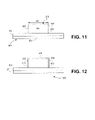
- FIG. 11 is a cross-sectional view of the fin 803 formed on the layer 802 covering the semiconductor substrate 801 to fabricate the non-planar transistor structure 800 according to one embodiment of the invention.
- the fin 803 has the top 808 and the two opposing sidewalls 809 , as shown in FIG. 11 .
- the fin 803 is formed by patterning and etching of a semiconductor layer 901 , which covers the layer 802 of the insulating material.
- the semiconductor layer 901 is doped to form a well in the semiconductor transistor structure as described above with respect to the transistor structure 121 .
- the concentration of the dopant to form the well is in the approximate range of 2 ⁇ 10 16 cm ⁇ 3 to 2 ⁇ 10 19 cm ⁇ 3 .
- a p-type dopant for example boron
- an n-type dopant for example As or P
- patterning and etching of the semiconductor layer 901 to form the fin 803 may be performed by techniques known to one of ordinary skill in the art of semiconductor fabrication.
- the width 902 of the fin 803 is in the approximate range of 20 nm to 120 nm.
- a diffusion barrier layer 806 is formed on the fin 803 , as described above with respect to the transistor structure 121 , as shown in FIG. 12 .
- the diffusion barrier layer 806 covers the top 808 and two opposing sidewalls 809 of the fin 803 .
- the diffusion barrier layer 806 is formed to suppress dopant outdiffusion from the fin 803 .
- the diffusion barrier layer 806 formed on the fin 803 is substantially thin.
- the thickness of the diffusion barrier layer 806 is in the approximate range of two to twenty atomic layers.
- the diffusion barrier layer 806 includes substitutional carbon (“C”).
- the diffusion barrier layer 806 on the fin 803 having Si can be made of any one of Si:C and SiGe:C material having the concentration of carbon in the approximate range of 10 17 cm ⁇ 3 to 2 ⁇ 10 21 cm ⁇ 3 .
- a semiconductor layer 807 is formed on the diffusion barrier layer 806 , as shown in FIG. 13 .
- the semiconductor layer 807 has substantially low dopant concentration relative to the dopant concentration in the fin 803 .
- the semiconductor layer 807 defines a channel of the non-planar transistor structure 800 with increased mobility of the carriers as described above with respect to the transistor structure 121 .
- the semiconductor layer 807 is on the diffusion barrier layer 806 along the top 808 and two opposing sidewalls 809 of the fin 803 .
- the semiconductor layer 807 may be formed using a technique described above with respect to the transistor structure 121 .
- the thickness of the semiconductor layer 807 formed on the diffusion barrier layer 806 is in the approximate range of 100 ⁇ to 1000 ⁇ .
- the dopant concentration in the semiconductor layer 807 is less than 10 16 cm ⁇ 3 .
- the semiconductor layer 807 formed on the diffusion barrier layer 806 covering the fin 803 having Si may be any one of an intrinsic Si and SiGe.
- FIG. 14 is a cross-sectional view of a non-planar semiconductor transistor structure 800 across the line A-A in FIG. 10 .
- the gate dielectric 804 and the tri-gate electrode 805 are subsequently formed on the semiconductor layer 807 as described above with respect to the transistor structure 121 .
- the semiconductor layer 807 sandwiched between the gate dielectric 804 and the diffusion barrier layer 806 defines the channel zone with increased mobility of the carriers in the non-planar transistor structure 800 .
- the gate dielectric 804 may include any one of silicon dioxide (“SiO 2 ”) or silicon nitride (“Si 3 N 4 ”).
- the gate dielectric 804 may include an oxide of a transition metal that has a dielectric constant k higher than the dielectric constant of SiO 2 , for example, zirconium oxide (“ZrO 2 ”), hafnium oxide (“HFO 2 ”), and lanthanum oxide (“La 2 O 4 ”).
- the thickness of the gate dielectric 804 may be between 5 ⁇ and 40 ⁇ .
- the thickness of the gate electrode 805 may be between 500 ⁇ and 3500 ⁇ .
- the gate electrode 805 includes any one of a polysilicon, polysilicon germanium, or the like metal.
Abstract
Description
Claims (28)
Priority Applications (1)
| Application Number | Priority Date | Filing Date | Title |
|---|---|---|---|
| US10/880,311 US7491988B2 (en) | 2004-06-28 | 2004-06-28 | Transistors with increased mobility in the channel zone and method of fabrication |
Applications Claiming Priority (1)
| Application Number | Priority Date | Filing Date | Title |
|---|---|---|---|
| US10/880,311 US7491988B2 (en) | 2004-06-28 | 2004-06-28 | Transistors with increased mobility in the channel zone and method of fabrication |
Publications (2)
| Publication Number | Publication Date |
|---|---|
| US20050285212A1 US20050285212A1 (en) | 2005-12-29 |
| US7491988B2 true US7491988B2 (en) | 2009-02-17 |
Family
ID=35504733
Family Applications (1)
| Application Number | Title | Priority Date | Filing Date |
|---|---|---|---|
| US10/880,311 Active US7491988B2 (en) | 2004-06-28 | 2004-06-28 | Transistors with increased mobility in the channel zone and method of fabrication |
Country Status (1)
| Country | Link |
|---|---|
| US (1) | US7491988B2 (en) |
Cited By (62)
| Publication number | Priority date | Publication date | Assignee | Title |
|---|---|---|---|---|
| US20100181625A1 (en) * | 2009-01-22 | 2010-07-22 | Kabushiki Kaisha Toshiba | Semiconductor device and method of fabricating the same |
| US20110074498A1 (en) * | 2009-09-30 | 2011-03-31 | Suvolta, Inc. | Electronic Devices and Systems, and Methods for Making and Using the Same |
| US20110079861A1 (en) * | 2009-09-30 | 2011-04-07 | Lucian Shifren | Advanced Transistors with Threshold Voltage Set Dopant Structures |
| US20110121404A1 (en) * | 2009-09-30 | 2011-05-26 | Lucian Shifren | Advanced transistors with punch through suppression |
| US8377783B2 (en) | 2010-09-30 | 2013-02-19 | Suvolta, Inc. | Method for reducing punch-through in a transistor device |
| US8400219B2 (en) | 2011-03-24 | 2013-03-19 | Suvolta, Inc. | Analog circuits having improved transistors, and methods therefor |
| US8404551B2 (en) | 2010-12-03 | 2013-03-26 | Suvolta, Inc. | Source/drain extension control for advanced transistors |
| US8461875B1 (en) | 2011-02-18 | 2013-06-11 | Suvolta, Inc. | Digital circuits having improved transistors, and methods therefor |
| WO2013095655A1 (en) * | 2011-12-23 | 2013-06-27 | Intel Corporation | Semiconductor device having germanium active layer with underlying diffusion barrier layer |
| US8525271B2 (en) | 2011-03-03 | 2013-09-03 | Suvolta, Inc. | Semiconductor structure with improved channel stack and method for fabrication thereof |
| US8530286B2 (en) | 2010-04-12 | 2013-09-10 | Suvolta, Inc. | Low power semiconductor transistor structure and method of fabrication thereof |
| US8569128B2 (en) | 2010-06-21 | 2013-10-29 | Suvolta, Inc. | Semiconductor structure and method of fabrication thereof with mixed metal types |
| US8569156B1 (en) | 2011-05-16 | 2013-10-29 | Suvolta, Inc. | Reducing or eliminating pre-amorphization in transistor manufacture |
| US8586455B1 (en) | 2012-05-15 | 2013-11-19 | International Business Machines Corporation | Preventing shorting of adjacent devices |
| US8599623B1 (en) | 2011-12-23 | 2013-12-03 | Suvolta, Inc. | Circuits and methods for measuring circuit elements in an integrated circuit device |
| US8614128B1 (en) | 2011-08-23 | 2013-12-24 | Suvolta, Inc. | CMOS structures and processes based on selective thinning |
| US8629016B1 (en) | 2011-07-26 | 2014-01-14 | Suvolta, Inc. | Multiple transistor types formed in a common epitaxial layer by differential out-diffusion from a doped underlayer |
| US8637955B1 (en) | 2012-08-31 | 2014-01-28 | Suvolta, Inc. | Semiconductor structure with reduced junction leakage and method of fabrication thereof |
| US8645878B1 (en) | 2011-08-23 | 2014-02-04 | Suvolta, Inc. | Porting a circuit design from a first semiconductor process to a second semiconductor process |
| US8713511B1 (en) | 2011-09-16 | 2014-04-29 | Suvolta, Inc. | Tools and methods for yield-aware semiconductor manufacturing process target generation |
| US8735987B1 (en) | 2011-06-06 | 2014-05-27 | Suvolta, Inc. | CMOS gate stack structures and processes |
| US8748986B1 (en) | 2011-08-05 | 2014-06-10 | Suvolta, Inc. | Electronic device with controlled threshold voltage |
| US8748270B1 (en) | 2011-03-30 | 2014-06-10 | Suvolta, Inc. | Process for manufacturing an improved analog transistor |
| US8748940B1 (en) | 2012-12-17 | 2014-06-10 | Intel Corporation | Semiconductor devices with germanium-rich active layers and doped transition layers |
| US8759872B2 (en) | 2010-06-22 | 2014-06-24 | Suvolta, Inc. | Transistor with threshold voltage set notch and method of fabrication thereof |
| US8796048B1 (en) | 2011-05-11 | 2014-08-05 | Suvolta, Inc. | Monitoring and measurement of thin film layers |
| US8811068B1 (en) | 2011-05-13 | 2014-08-19 | Suvolta, Inc. | Integrated circuit devices and methods |
| US8819603B1 (en) | 2011-12-15 | 2014-08-26 | Suvolta, Inc. | Memory circuits and methods of making and designing the same |
| US8816754B1 (en) | 2012-11-02 | 2014-08-26 | Suvolta, Inc. | Body bias circuits and methods |
| US8863064B1 (en) | 2012-03-23 | 2014-10-14 | Suvolta, Inc. | SRAM cell layout structure and devices therefrom |
| US8877619B1 (en) | 2012-01-23 | 2014-11-04 | Suvolta, Inc. | Process for manufacture of integrated circuits with different channel doping transistor architectures and devices therefrom |
| US8883600B1 (en) | 2011-12-22 | 2014-11-11 | Suvolta, Inc. | Transistor having reduced junction leakage and methods of forming thereof |
| US8895327B1 (en) | 2011-12-09 | 2014-11-25 | Suvolta, Inc. | Tipless transistors, short-tip transistors, and methods and circuits therefor |
| US8970289B1 (en) | 2012-01-23 | 2015-03-03 | Suvolta, Inc. | Circuits and devices for generating bi-directional body bias voltages, and methods therefor |
| US8976575B1 (en) | 2013-08-29 | 2015-03-10 | Suvolta, Inc. | SRAM performance monitor |
| US8988153B1 (en) | 2013-03-09 | 2015-03-24 | Suvolta, Inc. | Ring oscillator with NMOS or PMOS variation insensitivity |
| US8995204B2 (en) | 2011-06-23 | 2015-03-31 | Suvolta, Inc. | Circuit devices and methods having adjustable transistor body bias |
| US8994415B1 (en) | 2013-03-01 | 2015-03-31 | Suvolta, Inc. | Multiple VDD clock buffer |
| US8999861B1 (en) | 2011-05-11 | 2015-04-07 | Suvolta, Inc. | Semiconductor structure with substitutional boron and method for fabrication thereof |
| US9041126B2 (en) | 2012-09-21 | 2015-05-26 | Mie Fujitsu Semiconductor Limited | Deeply depleted MOS transistors having a screening layer and methods thereof |
| US9054219B1 (en) | 2011-08-05 | 2015-06-09 | Mie Fujitsu Semiconductor Limited | Semiconductor devices having fin structures and fabrication methods thereof |
| US9070477B1 (en) | 2012-12-12 | 2015-06-30 | Mie Fujitsu Semiconductor Limited | Bit interleaved low voltage static random access memory (SRAM) and related methods |
| US9093997B1 (en) | 2012-11-15 | 2015-07-28 | Mie Fujitsu Semiconductor Limited | Slew based process and bias monitors and related methods |
| US9093550B1 (en) | 2012-01-31 | 2015-07-28 | Mie Fujitsu Semiconductor Limited | Integrated circuits having a plurality of high-K metal gate FETs with various combinations of channel foundation structure and gate stack structure and methods of making same |
| US9112057B1 (en) | 2012-09-18 | 2015-08-18 | Mie Fujitsu Semiconductor Limited | Semiconductor devices with dopant migration suppression and method of fabrication thereof |
| US9112484B1 (en) | 2012-12-20 | 2015-08-18 | Mie Fujitsu Semiconductor Limited | Integrated circuit process and bias monitors and related methods |
| US9112495B1 (en) | 2013-03-15 | 2015-08-18 | Mie Fujitsu Semiconductor Limited | Integrated circuit device body bias circuits and methods |
| US9236466B1 (en) | 2011-10-07 | 2016-01-12 | Mie Fujitsu Semiconductor Limited | Analog circuits having improved insulated gate transistors, and methods therefor |
| US9263522B2 (en) | 2013-12-09 | 2016-02-16 | Qualcomm Incorporated | Transistor with a diffusion barrier |
| US9268885B1 (en) | 2013-02-28 | 2016-02-23 | Mie Fujitsu Semiconductor Limited | Integrated circuit device methods and models with predicted device metric variations |
| US9299801B1 (en) | 2013-03-14 | 2016-03-29 | Mie Fujitsu Semiconductor Limited | Method for fabricating a transistor device with a tuned dopant profile |
| US9299698B2 (en) | 2012-06-27 | 2016-03-29 | Mie Fujitsu Semiconductor Limited | Semiconductor structure with multiple transistors having various threshold voltages |
| US9319013B2 (en) | 2014-08-19 | 2016-04-19 | Mie Fujitsu Semiconductor Limited | Operational amplifier input offset correction with transistor threshold voltage adjustment |
| US9397165B2 (en) * | 2006-09-18 | 2016-07-19 | Intel Corporation | Active regions with compatible dielectric layers |
| US9406567B1 (en) | 2012-02-28 | 2016-08-02 | Mie Fujitsu Semiconductor Limited | Method for fabricating multiple transistor devices on a substrate with varying threshold voltages |
| US9431068B2 (en) | 2012-10-31 | 2016-08-30 | Mie Fujitsu Semiconductor Limited | Dynamic random access memory (DRAM) with low variation transistor peripheral circuits |
| US9449967B1 (en) | 2013-03-15 | 2016-09-20 | Fujitsu Semiconductor Limited | Transistor array structure |
| US9478571B1 (en) | 2013-05-24 | 2016-10-25 | Mie Fujitsu Semiconductor Limited | Buried channel deeply depleted channel transistor |
| US20170053994A1 (en) * | 2015-08-20 | 2017-02-23 | International Business Machines Corporation | Semiconductor structures having increased channel strain using fin release in gate regions |
| US9710006B2 (en) | 2014-07-25 | 2017-07-18 | Mie Fujitsu Semiconductor Limited | Power up body bias circuits and methods |
| US9825033B2 (en) | 2015-08-05 | 2017-11-21 | Samsung Electronics Co., Ltd. | Semiconductor devices and methods of manufacturing the same |
| US10991687B2 (en) * | 2016-04-29 | 2021-04-27 | Taiwan Semiconductor Manufacturing Co., Ltd. | FinFET varactor with low threshold voltage and method of making the same |
Families Citing this family (24)
| Publication number | Priority date | Publication date | Assignee | Title |
|---|---|---|---|---|
| US20060027833A1 (en) * | 2004-08-04 | 2006-02-09 | Nissan Motor Co., Ltd. | Silicon carbide semiconductor device and method of manufacturing the same |
| US7179696B2 (en) * | 2004-09-17 | 2007-02-20 | Texas Instruments Incorporated | Phosphorus activated NMOS using SiC process |
| US7691698B2 (en) * | 2006-02-21 | 2010-04-06 | International Business Machines Corporation | Pseudomorphic Si/SiGe/Si body device with embedded SiGe source/drain |
| US8154051B2 (en) * | 2006-08-29 | 2012-04-10 | Taiwan Semiconductor Manufacturing Co., Ltd. | MOS transistor with in-channel and laterally positioned stressors |
| US8450165B2 (en) | 2007-05-14 | 2013-05-28 | Intel Corporation | Semiconductor device having tipless epitaxial source/drain regions |
| KR100902105B1 (en) * | 2007-11-09 | 2009-06-09 | 주식회사 하이닉스반도체 | Method for manufacturing semiconductor device |
| US8330170B2 (en) * | 2008-12-05 | 2012-12-11 | Micron Technology, Inc. | Semiconductor device structures including transistors with energy barriers adjacent to transistor channels and associated methods |
| EP2202795A1 (en) * | 2008-12-24 | 2010-06-30 | S.O.I. TEC Silicon | Method for fabricating a semiconductor substrate and semiconductor substrate |
| US8753942B2 (en) * | 2010-12-01 | 2014-06-17 | Intel Corporation | Silicon and silicon germanium nanowire structures |
| US20140003122A1 (en) * | 2011-05-10 | 2014-01-02 | Fudan University | Semiconductor memory structure and control method thereof |
| US9153662B2 (en) * | 2012-03-29 | 2015-10-06 | Taiwan Semiconductor Manufacturing Company, Ltd. | MOSFET with selective dopant deactivation underneath gate |
| US8716090B2 (en) * | 2012-05-25 | 2014-05-06 | The Institute of Microelectronics Chinese Academy of Science | Semiconductor device manufacturing method |
| US9240354B2 (en) * | 2012-11-14 | 2016-01-19 | Globalfoundries Inc. | Semiconductor device having diffusion barrier to reduce back channel leakage |
| CN103943498B (en) * | 2013-01-22 | 2016-08-10 | 中芯国际集成电路制造(上海)有限公司 | Three-dimensional quantum well transistor and forming method thereof |
| US9972524B2 (en) * | 2013-03-11 | 2018-05-15 | Taiwan Semiconductor Manufacturing Company, Ltd. | Method for fabricating a semiconductor device |
| US9425099B2 (en) | 2014-01-16 | 2016-08-23 | Taiwan Semiconductor Manufacturing Co., Ltd. | Epitaxial channel with a counter-halo implant to improve analog gain |
| US9224814B2 (en) * | 2014-01-16 | 2015-12-29 | Taiwan Semiconductor Manufacturing Co., Ltd. | Process design to improve transistor variations and performance |
| US9236445B2 (en) | 2014-01-16 | 2016-01-12 | Taiwan Semiconductor Manufacturing Co., Ltd. | Transistor having replacement gate and epitaxially grown replacement channel region |
| US9184234B2 (en) | 2014-01-16 | 2015-11-10 | Taiwan Semiconductor Manufacturing Co., Ltd. | Transistor design |
| US9525031B2 (en) | 2014-03-13 | 2016-12-20 | Taiwan Semiconductor Manufacturing Co., Ltd. | Epitaxial channel |
| US9419136B2 (en) | 2014-04-14 | 2016-08-16 | Taiwan Semiconductor Manufacturing Co., Ltd. | Dislocation stress memorization technique (DSMT) on epitaxial channel devices |
| US9722045B2 (en) * | 2015-10-23 | 2017-08-01 | Globalfoundries Inc. | Buffer layer for modulating Vt across devices |
| US10276581B1 (en) | 2017-10-31 | 2019-04-30 | Taiwan Semiconductor Manufacturing Co., Ltd. | Integrated circuit chip and manufacturing method thereof |
| US20220320328A1 (en) * | 2021-04-06 | 2022-10-06 | Invention And Collaboration Laboratory Pte. Ltd. | Transistor structure and processing method therefore |
Citations (5)
| Publication number | Priority date | Publication date | Assignee | Title |
|---|---|---|---|---|
| US6271551B1 (en) * | 1995-12-15 | 2001-08-07 | U.S. Philips Corporation | Si-Ge CMOS semiconductor device |
| US20040099901A1 (en) * | 2002-11-14 | 2004-05-27 | Christoph Ludwig | Memory cell array |
| US20040256639A1 (en) * | 2003-06-17 | 2004-12-23 | International Business Machines Corporation | Low leakage heterojunction vertical transistors and high performance devices thereof |
| US20050093154A1 (en) * | 2003-07-25 | 2005-05-05 | Interuniversitair Microelektronica Centrum (Imec Vzw) | Multiple gate semiconductor device and method for forming same |
| US20050250289A1 (en) * | 2002-10-30 | 2005-11-10 | Babcock Jeffrey A | Control of dopant diffusion from buried layers in bipolar integrated circuits |
-
2004
- 2004-06-28 US US10/880,311 patent/US7491988B2/en active Active
Patent Citations (5)
| Publication number | Priority date | Publication date | Assignee | Title |
|---|---|---|---|---|
| US6271551B1 (en) * | 1995-12-15 | 2001-08-07 | U.S. Philips Corporation | Si-Ge CMOS semiconductor device |
| US20050250289A1 (en) * | 2002-10-30 | 2005-11-10 | Babcock Jeffrey A | Control of dopant diffusion from buried layers in bipolar integrated circuits |
| US20040099901A1 (en) * | 2002-11-14 | 2004-05-27 | Christoph Ludwig | Memory cell array |
| US20040256639A1 (en) * | 2003-06-17 | 2004-12-23 | International Business Machines Corporation | Low leakage heterojunction vertical transistors and high performance devices thereof |
| US20050093154A1 (en) * | 2003-07-25 | 2005-05-05 | Interuniversitair Microelektronica Centrum (Imec Vzw) | Multiple gate semiconductor device and method for forming same |
Non-Patent Citations (1)
| Title |
|---|
| H. Rucker et al., "Suppressed diffusion of boron and carbon in carbon-rich silicon", Applied Physics Letters, vol. 73, No. 12, Sep. 21, 1998, pp. 1682-1684, American Institute of Physics 1998. |
Cited By (139)
| Publication number | Priority date | Publication date | Assignee | Title |
|---|---|---|---|---|
| US9397165B2 (en) * | 2006-09-18 | 2016-07-19 | Intel Corporation | Active regions with compatible dielectric layers |
| US9847420B2 (en) | 2006-09-18 | 2017-12-19 | Intel Corporation | Active regions with compatible dielectric layers |
| US8134159B2 (en) * | 2009-01-22 | 2012-03-13 | Kabushiki Kaisha Toshiba | Semiconductor device including a p-type transistor having extension regions in sours and drain regions and method of fabricating the same |
| US20100181625A1 (en) * | 2009-01-22 | 2010-07-22 | Kabushiki Kaisha Toshiba | Semiconductor device and method of fabricating the same |
| US10217668B2 (en) | 2009-09-30 | 2019-02-26 | Mie Fujitsu Semiconductor Limited | Electronic devices and systems, and methods for making and using the same |
| US9263523B2 (en) | 2009-09-30 | 2016-02-16 | Mie Fujitsu Semiconductor Limited | Advanced transistors with punch through suppression |
| US10325986B2 (en) | 2009-09-30 | 2019-06-18 | Mie Fujitsu Semiconductor Limited | Advanced transistors with punch through suppression |
| US8273617B2 (en) | 2009-09-30 | 2012-09-25 | Suvolta, Inc. | Electronic devices and systems, and methods for making and using the same |
| US20110121404A1 (en) * | 2009-09-30 | 2011-05-26 | Lucian Shifren | Advanced transistors with punch through suppression |
| US8421162B2 (en) | 2009-09-30 | 2013-04-16 | Suvolta, Inc. | Advanced transistors with punch through suppression |
| US20110079861A1 (en) * | 2009-09-30 | 2011-04-07 | Lucian Shifren | Advanced Transistors with Threshold Voltage Set Dopant Structures |
| US11887895B2 (en) | 2009-09-30 | 2024-01-30 | United Semiconductor Japan Co., Ltd. | Electronic devices and systems, and methods for making and using the same |
| US10224244B2 (en) | 2009-09-30 | 2019-03-05 | Mie Fujitsu Semiconductor Limited | Electronic devices and systems, and methods for making and using the same |
| US9508800B2 (en) | 2009-09-30 | 2016-11-29 | Mie Fujitsu Semiconductor Limited | Advanced transistors with punch through suppression |
| US8541824B2 (en) | 2009-09-30 | 2013-09-24 | Suvolta, Inc. | Electronic devices and systems, and methods for making and using the same |
| US10074568B2 (en) | 2009-09-30 | 2018-09-11 | Mie Fujitsu Semiconductor Limited | Electronic devices and systems, and methods for making and using same |
| US8604527B2 (en) | 2009-09-30 | 2013-12-10 | Suvolta, Inc. | Electronic devices and systems, and methods for making and using the same |
| US8975128B2 (en) | 2009-09-30 | 2015-03-10 | Suvolta, Inc. | Electronic devices and systems, and methods for making and using the same |
| US20110074498A1 (en) * | 2009-09-30 | 2011-03-31 | Suvolta, Inc. | Electronic Devices and Systems, and Methods for Making and Using the Same |
| US11062950B2 (en) | 2009-09-30 | 2021-07-13 | United Semiconductor Japan Co., Ltd. | Electronic devices and systems, and methods for making and using the same |
| US8604530B2 (en) | 2009-09-30 | 2013-12-10 | Suvolta, Inc. | Electronic devices and systems, and methods for making and using the same |
| US9865596B2 (en) | 2010-04-12 | 2018-01-09 | Mie Fujitsu Semiconductor Limited | Low power semiconductor transistor structure and method of fabrication thereof |
| US9496261B2 (en) | 2010-04-12 | 2016-11-15 | Mie Fujitsu Semiconductor Limited | Low power semiconductor transistor structure and method of fabrication thereof |
| US8530286B2 (en) | 2010-04-12 | 2013-09-10 | Suvolta, Inc. | Low power semiconductor transistor structure and method of fabrication thereof |
| US8569128B2 (en) | 2010-06-21 | 2013-10-29 | Suvolta, Inc. | Semiconductor structure and method of fabrication thereof with mixed metal types |
| US9224733B2 (en) | 2010-06-21 | 2015-12-29 | Mie Fujitsu Semiconductor Limited | Semiconductor structure and method of fabrication thereof with mixed metal types |
| US8759872B2 (en) | 2010-06-22 | 2014-06-24 | Suvolta, Inc. | Transistor with threshold voltage set notch and method of fabrication thereof |
| US9418987B2 (en) | 2010-06-22 | 2016-08-16 | Mie Fujitsu Semiconductor Limited | Transistor with threshold voltage set notch and method of fabrication thereof |
| US9922977B2 (en) | 2010-06-22 | 2018-03-20 | Mie Fujitsu Semiconductor Limited | Transistor with threshold voltage set notch and method of fabrication thereof |
| US8377783B2 (en) | 2010-09-30 | 2013-02-19 | Suvolta, Inc. | Method for reducing punch-through in a transistor device |
| US8686511B2 (en) | 2010-12-03 | 2014-04-01 | Suvolta, Inc. | Source/drain extension control for advanced transistors |
| US8404551B2 (en) | 2010-12-03 | 2013-03-26 | Suvolta, Inc. | Source/drain extension control for advanced transistors |
| US9006843B2 (en) | 2010-12-03 | 2015-04-14 | Suvolta, Inc. | Source/drain extension control for advanced transistors |
| US8563384B2 (en) | 2010-12-03 | 2013-10-22 | Suvolta, Inc. | Source/drain extension control for advanced transistors |
| US9184750B1 (en) | 2011-02-18 | 2015-11-10 | Mie Fujitsu Semiconductor Limited | Digital circuits having improved transistors, and methods therefor |
| US9680470B2 (en) | 2011-02-18 | 2017-06-13 | Mie Fujitsu Semiconductor Limited | Digital circuits having improved transistors, and methods therefor |
| US10250257B2 (en) | 2011-02-18 | 2019-04-02 | Mie Fujitsu Semiconductor Limited | Digital circuits having improved transistors, and methods therefor |
| US9838012B2 (en) | 2011-02-18 | 2017-12-05 | Mie Fujitsu Semiconductor Limited | Digital circuits having improved transistors, and methods therefor |
| US8461875B1 (en) | 2011-02-18 | 2013-06-11 | Suvolta, Inc. | Digital circuits having improved transistors, and methods therefor |
| US9985631B2 (en) | 2011-02-18 | 2018-05-29 | Mie Fujitsu Semiconductor Limited | Digital circuits having improved transistors, and methods therefor |
| US8525271B2 (en) | 2011-03-03 | 2013-09-03 | Suvolta, Inc. | Semiconductor structure with improved channel stack and method for fabrication thereof |
| US9111785B2 (en) | 2011-03-03 | 2015-08-18 | Mie Fujitsu Semiconductor Limited | Semiconductor structure with improved channel stack and method for fabrication thereof |
| US8847684B2 (en) | 2011-03-24 | 2014-09-30 | Suvolta, Inc. | Analog circuits having improved transistors, and methods therefor |
| US9231541B2 (en) | 2011-03-24 | 2016-01-05 | Mie Fujitsu Semiconductor Limited | Analog circuits having improved transistors, and methods therefor |
| US8400219B2 (en) | 2011-03-24 | 2013-03-19 | Suvolta, Inc. | Analog circuits having improved transistors, and methods therefor |
| US8748270B1 (en) | 2011-03-30 | 2014-06-10 | Suvolta, Inc. | Process for manufacturing an improved analog transistor |
| US9093469B2 (en) | 2011-03-30 | 2015-07-28 | Mie Fujitsu Semiconductor Limited | Analog transistor |
| US8796048B1 (en) | 2011-05-11 | 2014-08-05 | Suvolta, Inc. | Monitoring and measurement of thin film layers |
| US8999861B1 (en) | 2011-05-11 | 2015-04-07 | Suvolta, Inc. | Semiconductor structure with substitutional boron and method for fabrication thereof |
| US9741428B2 (en) | 2011-05-13 | 2017-08-22 | Mie Fujitsu Semiconductor Limited | Integrated circuit devices and methods |
| US9362291B1 (en) | 2011-05-13 | 2016-06-07 | Mie Fujitsu Semiconductor Limited | Integrated circuit devices and methods |
| US9966130B2 (en) | 2011-05-13 | 2018-05-08 | Mie Fujitsu Semiconductor Limited | Integrated circuit devices and methods |
| US8811068B1 (en) | 2011-05-13 | 2014-08-19 | Suvolta, Inc. | Integrated circuit devices and methods |
| US8937005B2 (en) | 2011-05-16 | 2015-01-20 | Suvolta, Inc. | Reducing or eliminating pre-amorphization in transistor manufacture |
| US9793172B2 (en) | 2011-05-16 | 2017-10-17 | Mie Fujitsu Semiconductor Limited | Reducing or eliminating pre-amorphization in transistor manufacture |
| US8569156B1 (en) | 2011-05-16 | 2013-10-29 | Suvolta, Inc. | Reducing or eliminating pre-amorphization in transistor manufacture |
| US9514940B2 (en) | 2011-05-16 | 2016-12-06 | Mie Fujitsu Semiconductor Limited | Reducing or eliminating pre-amorphization in transistor manufacture |
| US9281248B1 (en) | 2011-06-06 | 2016-03-08 | Mie Fujitsu Semiconductor Limited | CMOS gate stack structures and processes |
| US9508728B2 (en) | 2011-06-06 | 2016-11-29 | Mie Fujitsu Semiconductor Limited | CMOS gate stack structures and processes |
| US8735987B1 (en) | 2011-06-06 | 2014-05-27 | Suvolta, Inc. | CMOS gate stack structures and processes |
| US8995204B2 (en) | 2011-06-23 | 2015-03-31 | Suvolta, Inc. | Circuit devices and methods having adjustable transistor body bias |
| US8629016B1 (en) | 2011-07-26 | 2014-01-14 | Suvolta, Inc. | Multiple transistor types formed in a common epitaxial layer by differential out-diffusion from a doped underlayer |
| US8653604B1 (en) | 2011-07-26 | 2014-02-18 | Suvolta, Inc. | Multiple transistor types formed in a common epitaxial layer by differential out-diffusion from a doped underlayer |
| US8916937B1 (en) | 2011-07-26 | 2014-12-23 | Suvolta, Inc. | Multiple transistor types formed in a common epitaxial layer by differential out-diffusion from a doped underlayer |
| US8748986B1 (en) | 2011-08-05 | 2014-06-10 | Suvolta, Inc. | Electronic device with controlled threshold voltage |
| US9054219B1 (en) | 2011-08-05 | 2015-06-09 | Mie Fujitsu Semiconductor Limited | Semiconductor devices having fin structures and fabrication methods thereof |
| US8963249B1 (en) | 2011-08-05 | 2015-02-24 | Suvolta, Inc. | Electronic device with controlled threshold voltage |
| US8614128B1 (en) | 2011-08-23 | 2013-12-24 | Suvolta, Inc. | CMOS structures and processes based on selective thinning |
| US8806395B1 (en) | 2011-08-23 | 2014-08-12 | Suvolta, Inc. | Porting a circuit design from a first semiconductor process to a second semiconductor process |
| US9391076B1 (en) | 2011-08-23 | 2016-07-12 | Mie Fujitsu Semiconductor Limited | CMOS structures and processes based on selective thinning |
| US8645878B1 (en) | 2011-08-23 | 2014-02-04 | Suvolta, Inc. | Porting a circuit design from a first semiconductor process to a second semiconductor process |
| US9117746B1 (en) | 2011-08-23 | 2015-08-25 | Mie Fujitsu Semiconductor Limited | Porting a circuit design from a first semiconductor process to a second semiconductor process |
| US8713511B1 (en) | 2011-09-16 | 2014-04-29 | Suvolta, Inc. | Tools and methods for yield-aware semiconductor manufacturing process target generation |
| US9236466B1 (en) | 2011-10-07 | 2016-01-12 | Mie Fujitsu Semiconductor Limited | Analog circuits having improved insulated gate transistors, and methods therefor |
| US10573644B2 (en) | 2011-12-09 | 2020-02-25 | Mie Fujitsu Semiconductor Limited | Tipless transistors, short-tip transistors, and methods and circuits therefor |
| US9953974B2 (en) | 2011-12-09 | 2018-04-24 | Mie Fujitsu Semiconductor Limited | Tipless transistors, short-tip transistors, and methods and circuits therefor |
| US9583484B2 (en) | 2011-12-09 | 2017-02-28 | Mie Fujitsu Semiconductor Limited | Tipless transistors, short-tip transistors, and methods and circuits therefor |
| US11145647B2 (en) | 2011-12-09 | 2021-10-12 | United Semiconductor Japan Co., Ltd. | Tipless transistors, short-tip transistors, and methods and circuits therefor |
| US8895327B1 (en) | 2011-12-09 | 2014-11-25 | Suvolta, Inc. | Tipless transistors, short-tip transistors, and methods and circuits therefor |
| US9385121B1 (en) | 2011-12-09 | 2016-07-05 | Mie Fujitsu Semiconductor Limited | Tipless transistors, short-tip transistors, and methods and circuits therefor |
| US8819603B1 (en) | 2011-12-15 | 2014-08-26 | Suvolta, Inc. | Memory circuits and methods of making and designing the same |
| US9196727B2 (en) | 2011-12-22 | 2015-11-24 | Mie Fujitsu Semiconductor Limited | High uniformity screen and epitaxial layers for CMOS devices |
| US8883600B1 (en) | 2011-12-22 | 2014-11-11 | Suvolta, Inc. | Transistor having reduced junction leakage and methods of forming thereof |
| US9368624B2 (en) | 2011-12-22 | 2016-06-14 | Mie Fujitsu Semiconductor Limited | Method for fabricating a transistor with reduced junction leakage current |
| WO2013095655A1 (en) * | 2011-12-23 | 2013-06-27 | Intel Corporation | Semiconductor device having germanium active layer with underlying diffusion barrier layer |
| US8599623B1 (en) | 2011-12-23 | 2013-12-03 | Suvolta, Inc. | Circuits and methods for measuring circuit elements in an integrated circuit device |
| US9297850B1 (en) | 2011-12-23 | 2016-03-29 | Mie Fujitsu Semiconductor Limited | Circuits and methods for measuring circuit elements in an integrated circuit device |
| US9608055B2 (en) | 2011-12-23 | 2017-03-28 | Intel Corporation | Semiconductor device having germanium active layer with underlying diffusion barrier layer |
| US10186580B2 (en) | 2011-12-23 | 2019-01-22 | Intel Corporation | Semiconductor device having germanium active layer with underlying diffusion barrier layer |
| US8970289B1 (en) | 2012-01-23 | 2015-03-03 | Suvolta, Inc. | Circuits and devices for generating bi-directional body bias voltages, and methods therefor |
| US8877619B1 (en) | 2012-01-23 | 2014-11-04 | Suvolta, Inc. | Process for manufacture of integrated circuits with different channel doping transistor architectures and devices therefrom |
| US9093550B1 (en) | 2012-01-31 | 2015-07-28 | Mie Fujitsu Semiconductor Limited | Integrated circuits having a plurality of high-K metal gate FETs with various combinations of channel foundation structure and gate stack structure and methods of making same |
| US9385047B2 (en) | 2012-01-31 | 2016-07-05 | Mie Fujitsu Semiconductor Limited | Integrated circuits having a plurality of high-K metal gate FETs with various combinations of channel foundation structure and gate stack structure and methods of making same |
| US9406567B1 (en) | 2012-02-28 | 2016-08-02 | Mie Fujitsu Semiconductor Limited | Method for fabricating multiple transistor devices on a substrate with varying threshold voltages |
| US9424385B1 (en) | 2012-03-23 | 2016-08-23 | Mie Fujitsu Semiconductor Limited | SRAM cell layout structure and devices therefrom |
| US8863064B1 (en) | 2012-03-23 | 2014-10-14 | Suvolta, Inc. | SRAM cell layout structure and devices therefrom |
| US8586455B1 (en) | 2012-05-15 | 2013-11-19 | International Business Machines Corporation | Preventing shorting of adjacent devices |
| US10014387B2 (en) | 2012-06-27 | 2018-07-03 | Mie Fujitsu Semiconductor Limited | Semiconductor structure with multiple transistors having various threshold voltages |
| US9299698B2 (en) | 2012-06-27 | 2016-03-29 | Mie Fujitsu Semiconductor Limited | Semiconductor structure with multiple transistors having various threshold voltages |
| US9812550B2 (en) | 2012-06-27 | 2017-11-07 | Mie Fujitsu Semiconductor Limited | Semiconductor structure with multiple transistors having various threshold voltages |
| US10217838B2 (en) | 2012-06-27 | 2019-02-26 | Mie Fujitsu Semiconductor Limited | Semiconductor structure with multiple transistors having various threshold voltages |
| US9105711B2 (en) | 2012-08-31 | 2015-08-11 | Mie Fujitsu Semiconductor Limited | Semiconductor structure with reduced junction leakage and method of fabrication thereof |
| US8637955B1 (en) | 2012-08-31 | 2014-01-28 | Suvolta, Inc. | Semiconductor structure with reduced junction leakage and method of fabrication thereof |
| US9112057B1 (en) | 2012-09-18 | 2015-08-18 | Mie Fujitsu Semiconductor Limited | Semiconductor devices with dopant migration suppression and method of fabrication thereof |
| US9041126B2 (en) | 2012-09-21 | 2015-05-26 | Mie Fujitsu Semiconductor Limited | Deeply depleted MOS transistors having a screening layer and methods thereof |
| US9431068B2 (en) | 2012-10-31 | 2016-08-30 | Mie Fujitsu Semiconductor Limited | Dynamic random access memory (DRAM) with low variation transistor peripheral circuits |
| US8816754B1 (en) | 2012-11-02 | 2014-08-26 | Suvolta, Inc. | Body bias circuits and methods |
| US9154123B1 (en) | 2012-11-02 | 2015-10-06 | Mie Fujitsu Semiconductor Limited | Body bias circuits and methods |
| US9093997B1 (en) | 2012-11-15 | 2015-07-28 | Mie Fujitsu Semiconductor Limited | Slew based process and bias monitors and related methods |
| US9319034B2 (en) | 2012-11-15 | 2016-04-19 | Mie Fujitsu Semiconductor Limited | Slew based process and bias monitors and related methods |
| US9070477B1 (en) | 2012-12-12 | 2015-06-30 | Mie Fujitsu Semiconductor Limited | Bit interleaved low voltage static random access memory (SRAM) and related methods |
| US8748940B1 (en) | 2012-12-17 | 2014-06-10 | Intel Corporation | Semiconductor devices with germanium-rich active layers and doped transition layers |
| US9276561B2 (en) | 2012-12-20 | 2016-03-01 | Mie Fujitsu Semiconductor Limited | Integrated circuit process and bias monitors and related methods |
| US9112484B1 (en) | 2012-12-20 | 2015-08-18 | Mie Fujitsu Semiconductor Limited | Integrated circuit process and bias monitors and related methods |
| US9268885B1 (en) | 2013-02-28 | 2016-02-23 | Mie Fujitsu Semiconductor Limited | Integrated circuit device methods and models with predicted device metric variations |
| US8994415B1 (en) | 2013-03-01 | 2015-03-31 | Suvolta, Inc. | Multiple VDD clock buffer |
| US8988153B1 (en) | 2013-03-09 | 2015-03-24 | Suvolta, Inc. | Ring oscillator with NMOS or PMOS variation insensitivity |
| US9893148B2 (en) | 2013-03-14 | 2018-02-13 | Mie Fujitsu Semiconductor Limited | Method for fabricating a transistor device with a tuned dopant profile |
| US9299801B1 (en) | 2013-03-14 | 2016-03-29 | Mie Fujitsu Semiconductor Limited | Method for fabricating a transistor device with a tuned dopant profile |
| US9577041B2 (en) | 2013-03-14 | 2017-02-21 | Mie Fujitsu Semiconductor Limited | Method for fabricating a transistor device with a tuned dopant profile |
| US9112495B1 (en) | 2013-03-15 | 2015-08-18 | Mie Fujitsu Semiconductor Limited | Integrated circuit device body bias circuits and methods |
| US9548086B2 (en) | 2013-03-15 | 2017-01-17 | Mie Fujitsu Semiconductor Limited | Integrated circuit device body bias circuits and methods |
| US9853019B2 (en) | 2013-03-15 | 2017-12-26 | Mie Fujitsu Semiconductor Limited | Integrated circuit device body bias circuits and methods |
| US9449967B1 (en) | 2013-03-15 | 2016-09-20 | Fujitsu Semiconductor Limited | Transistor array structure |
| US9991300B2 (en) | 2013-05-24 | 2018-06-05 | Mie Fujitsu Semiconductor Limited | Buried channel deeply depleted channel transistor |
| US9786703B2 (en) | 2013-05-24 | 2017-10-10 | Mie Fujitsu Semiconductor Limited | Buried channel deeply depleted channel transistor |
| US9478571B1 (en) | 2013-05-24 | 2016-10-25 | Mie Fujitsu Semiconductor Limited | Buried channel deeply depleted channel transistor |
| US8976575B1 (en) | 2013-08-29 | 2015-03-10 | Suvolta, Inc. | SRAM performance monitor |
| US9263522B2 (en) | 2013-12-09 | 2016-02-16 | Qualcomm Incorporated | Transistor with a diffusion barrier |
| US9710006B2 (en) | 2014-07-25 | 2017-07-18 | Mie Fujitsu Semiconductor Limited | Power up body bias circuits and methods |
| US9319013B2 (en) | 2014-08-19 | 2016-04-19 | Mie Fujitsu Semiconductor Limited | Operational amplifier input offset correction with transistor threshold voltage adjustment |
| US9825033B2 (en) | 2015-08-05 | 2017-11-21 | Samsung Electronics Co., Ltd. | Semiconductor devices and methods of manufacturing the same |
| US20170053994A1 (en) * | 2015-08-20 | 2017-02-23 | International Business Machines Corporation | Semiconductor structures having increased channel strain using fin release in gate regions |
| US10886385B2 (en) | 2015-08-20 | 2021-01-05 | International Business Machines Corporation | Semiconductor structures having increased channel strain using fin release in gate regions |
| US20170053839A1 (en) * | 2015-08-20 | 2017-02-23 | International Business Machines Corporation | Semiconductor structures having increased channel strain using fin release in gate regions |
| US10056474B2 (en) * | 2015-08-20 | 2018-08-21 | International Business Machines Corporation | Semiconductor structures having increased channel strain using fin release in gate regions |
| US9954083B2 (en) * | 2015-08-20 | 2018-04-24 | International Business Machines Corporation | Semiconductor structures having increased channel strain using fin release in gate regions |
| US10991687B2 (en) * | 2016-04-29 | 2021-04-27 | Taiwan Semiconductor Manufacturing Co., Ltd. | FinFET varactor with low threshold voltage and method of making the same |
| US11532614B2 (en) | 2016-04-29 | 2022-12-20 | Taiwan Semiconductor Manufacturing Co., Ltd. | FinFET varactor with low threshold voltage and method of making the same |
Also Published As
| Publication number | Publication date |
|---|---|
| US20050285212A1 (en) | 2005-12-29 |
Similar Documents
| Publication | Publication Date | Title |
|---|---|---|
| US7491988B2 (en) | Transistors with increased mobility in the channel zone and method of fabrication | |
| US7023018B2 (en) | SiGe transistor with strained layers | |
| KR100845175B1 (en) | A bulk non-planar transistor having a strained channel with enhanced mobility and methods of fabrication | |
| US6844227B2 (en) | Semiconductor devices and method for manufacturing the same | |
| US7960798B2 (en) | Structure and method to form multilayer embedded stressors | |
| US7348284B2 (en) | Non-planar pMOS structure with a strained channel region and an integrated strained CMOS flow | |
| JP3544833B2 (en) | Semiconductor device and manufacturing method thereof | |
| US5349225A (en) | Field effect transistor with a lightly doped drain | |
| US9490364B2 (en) | Semiconductor transistor having a stressed channel | |
| US20020115240A1 (en) | Double soi device with recess etch and epitaxy | |
| US20070284628A1 (en) | Self aligned gate JFET structure and method | |
| US8399933B2 (en) | Semiconductor device having silicon on stressed liner (SOL) | |
| US20100289086A1 (en) | Source/Drain Strained Layers | |
| US20080169490A1 (en) | Semiconductor device and manufacturing method thereof | |
| US20080272395A1 (en) | Enhanced hole mobility p-type jfet and fabrication method therefor | |
| US6818938B1 (en) | MOS transistor and method of forming the transistor with a channel region in a layer of composite material | |
| US8759168B2 (en) | MOSFET with thin semiconductor channel and embedded stressor with enhanced junction isolation and method of fabrication | |
| KR100760912B1 (en) | Semiconductor Device and Method for Fabricating The Same | |
| CN115458603A (en) | Semiconductor device structure and preparation method thereof | |
| CN116635985A (en) | Field effect transistor and method of manufacturing the same |
Legal Events
| Date | Code | Title | Description |
|---|---|---|---|
| AS | Assignment |
Owner name: INTEL CORPORATION, CALIFORNIA Free format text: ASSIGNMENT OF ASSIGNORS INTEREST;ASSIGNORS:TOLCHINSKY, PETER G.;BOHR, MARK;YABLOK, IRWIN;REEL/FRAME:015777/0456 Effective date: 20040903 |
|
| STCF | Information on status: patent grant |
Free format text: PATENTED CASE |
|
| REMI | Maintenance fee reminder mailed | ||
| FPAY | Fee payment |
Year of fee payment: 4 |
|
| SULP | Surcharge for late payment | ||
| FPAY | Fee payment |
Year of fee payment: 8 |
|
| MAFP | Maintenance fee payment |
Free format text: PAYMENT OF MAINTENANCE FEE, 12TH YEAR, LARGE ENTITY (ORIGINAL EVENT CODE: M1553); ENTITY STATUS OF PATENT OWNER: LARGE ENTITY Year of fee payment: 12 |
|
| AS | Assignment |
Owner name: TAHOE RESEARCH, LTD., IRELAND Free format text: ASSIGNMENT OF ASSIGNORS INTEREST;ASSIGNOR:INTEL CORPORATION;REEL/FRAME:061175/0176 Effective date: 20220718 |