US7279774B2 - Bulk substrates in FinFETs with trench insulation surrounding FIN pairs having FINs separated by recess hole shallower than trench - Google Patents
Bulk substrates in FinFETs with trench insulation surrounding FIN pairs having FINs separated by recess hole shallower than trench Download PDFInfo
- Publication number
- US7279774B2 US7279774B2 US10/938,436 US93843604A US7279774B2 US 7279774 B2 US7279774 B2 US 7279774B2 US 93843604 A US93843604 A US 93843604A US 7279774 B2 US7279774 B2 US 7279774B2
- Authority
- US
- United States
- Prior art keywords
- trench
- channel
- insulating layer
- recess hole
- cross
- Prior art date
- Legal status (The legal status is an assumption and is not a legal conclusion. Google has not performed a legal analysis and makes no representation as to the accuracy of the status listed.)
- Expired - Fee Related, expires
Links
- 239000000758 substrate Substances 0.000 title claims abstract description 41
- 238000009413 insulation Methods 0.000 title 1
- 239000004065 semiconductor Substances 0.000 claims abstract description 27
- 230000005669 field effect Effects 0.000 claims description 3
- 239000010410 layer Substances 0.000 description 48
- 238000010586 diagram Methods 0.000 description 28
- 238000000034 method Methods 0.000 description 14
- 125000006850 spacer group Chemical group 0.000 description 14
- 238000004519 manufacturing process Methods 0.000 description 9
- 150000004767 nitrides Chemical class 0.000 description 8
- 238000005530 etching Methods 0.000 description 6
- NBIIXXVUZAFLBC-UHFFFAOYSA-N Phosphoric acid Chemical compound OP(O)(O)=O NBIIXXVUZAFLBC-UHFFFAOYSA-N 0.000 description 4
- 239000011810 insulating material Substances 0.000 description 4
- XUIMIQQOPSSXEZ-UHFFFAOYSA-N Silicon Chemical compound [Si] XUIMIQQOPSSXEZ-UHFFFAOYSA-N 0.000 description 3
- 239000011247 coating layer Substances 0.000 description 3
- 229910052710 silicon Inorganic materials 0.000 description 3
- 239000010703 silicon Substances 0.000 description 3
- 229910000147 aluminium phosphate Inorganic materials 0.000 description 2
- 239000006117 anti-reflective coating Substances 0.000 description 2
- 239000012535 impurity Substances 0.000 description 2
- 239000002184 metal Substances 0.000 description 2
- 229910052751 metal Inorganic materials 0.000 description 2
- RYGMFSIKBFXOCR-UHFFFAOYSA-N Copper Chemical compound [Cu] RYGMFSIKBFXOCR-UHFFFAOYSA-N 0.000 description 1
- 239000000853 adhesive Substances 0.000 description 1
- 230000001070 adhesive effect Effects 0.000 description 1
- 239000004020 conductor Substances 0.000 description 1
- 229910052802 copper Inorganic materials 0.000 description 1
- 239000010949 copper Substances 0.000 description 1
- 230000009977 dual effect Effects 0.000 description 1
- 238000002955 isolation Methods 0.000 description 1
- 238000005498 polishing Methods 0.000 description 1
- 239000000126 substance Substances 0.000 description 1
Images


Classifications
-
- H—ELECTRICITY
- H01—ELECTRIC ELEMENTS
- H01L—SEMICONDUCTOR DEVICES NOT COVERED BY CLASS H10
- H01L29/00—Semiconductor devices adapted for rectifying, amplifying, oscillating or switching, or capacitors or resistors with at least one potential-jump barrier or surface barrier, e.g. PN junction depletion layer or carrier concentration layer; Details of semiconductor bodies or of electrodes thereof ; Multistep manufacturing processes therefor
- H01L29/66—Types of semiconductor device ; Multistep manufacturing processes therefor
- H01L29/68—Types of semiconductor device ; Multistep manufacturing processes therefor controllable by only the electric current supplied, or only the electric potential applied, to an electrode which does not carry the current to be rectified, amplified or switched
- H01L29/76—Unipolar devices, e.g. field effect transistors
- H01L29/772—Field effect transistors
- H01L29/78—Field effect transistors with field effect produced by an insulated gate
- H01L29/785—Field effect transistors with field effect produced by an insulated gate having a channel with a horizontal current flow in a vertical sidewall of a semiconductor body, e.g. FinFET, MuGFET
-
- H—ELECTRICITY
- H01—ELECTRIC ELEMENTS
- H01L—SEMICONDUCTOR DEVICES NOT COVERED BY CLASS H10
- H01L29/00—Semiconductor devices adapted for rectifying, amplifying, oscillating or switching, or capacitors or resistors with at least one potential-jump barrier or surface barrier, e.g. PN junction depletion layer or carrier concentration layer; Details of semiconductor bodies or of electrodes thereof ; Multistep manufacturing processes therefor
- H01L29/66—Types of semiconductor device ; Multistep manufacturing processes therefor
- H01L29/66007—Multistep manufacturing processes
- H01L29/66075—Multistep manufacturing processes of devices having semiconductor bodies comprising group 14 or group 13/15 materials
- H01L29/66227—Multistep manufacturing processes of devices having semiconductor bodies comprising group 14 or group 13/15 materials the devices being controllable only by the electric current supplied or the electric potential applied, to an electrode which does not carry the current to be rectified, amplified or switched, e.g. three-terminal devices
- H01L29/66409—Unipolar field-effect transistors
- H01L29/66477—Unipolar field-effect transistors with an insulated gate, i.e. MISFET
- H01L29/66787—Unipolar field-effect transistors with an insulated gate, i.e. MISFET with a gate at the side of the channel
- H01L29/66795—Unipolar field-effect transistors with an insulated gate, i.e. MISFET with a gate at the side of the channel with a horizontal current flow in a vertical sidewall of a semiconductor body, e.g. FinFET, MuGFET
-
- H—ELECTRICITY
- H01—ELECTRIC ELEMENTS
- H01L—SEMICONDUCTOR DEVICES NOT COVERED BY CLASS H10
- H01L21/00—Processes or apparatus adapted for the manufacture or treatment of semiconductor or solid state devices or of parts thereof
- H01L21/70—Manufacture or treatment of devices consisting of a plurality of solid state components formed in or on a common substrate or of parts thereof; Manufacture of integrated circuit devices or of parts thereof
- H01L21/71—Manufacture of specific parts of devices defined in group H01L21/70
- H01L21/76—Making of isolation regions between components
- H01L21/762—Dielectric regions, e.g. EPIC dielectric isolation, LOCOS; Trench refilling techniques, SOI technology, use of channel stoppers
- H01L21/76202—Dielectric regions, e.g. EPIC dielectric isolation, LOCOS; Trench refilling techniques, SOI technology, use of channel stoppers using a local oxidation of silicon, e.g. LOCOS, SWAMI, SILO
- H01L21/76205—Dielectric regions, e.g. EPIC dielectric isolation, LOCOS; Trench refilling techniques, SOI technology, use of channel stoppers using a local oxidation of silicon, e.g. LOCOS, SWAMI, SILO in a region being recessed from the surface, e.g. in a recess, groove, tub or trench region
-
- H—ELECTRICITY
- H01—ELECTRIC ELEMENTS
- H01L—SEMICONDUCTOR DEVICES NOT COVERED BY CLASS H10
- H01L29/00—Semiconductor devices adapted for rectifying, amplifying, oscillating or switching, or capacitors or resistors with at least one potential-jump barrier or surface barrier, e.g. PN junction depletion layer or carrier concentration layer; Details of semiconductor bodies or of electrodes thereof ; Multistep manufacturing processes therefor
- H01L29/40—Electrodes ; Multistep manufacturing processes therefor
- H01L29/41—Electrodes ; Multistep manufacturing processes therefor characterised by their shape, relative sizes or dispositions
- H01L29/423—Electrodes ; Multistep manufacturing processes therefor characterised by their shape, relative sizes or dispositions not carrying the current to be rectified, amplified or switched
- H01L29/42312—Gate electrodes for field effect devices
-
- H—ELECTRICITY
- H01—ELECTRIC ELEMENTS
- H01L—SEMICONDUCTOR DEVICES NOT COVERED BY CLASS H10
- H01L29/00—Semiconductor devices adapted for rectifying, amplifying, oscillating or switching, or capacitors or resistors with at least one potential-jump barrier or surface barrier, e.g. PN junction depletion layer or carrier concentration layer; Details of semiconductor bodies or of electrodes thereof ; Multistep manufacturing processes therefor
- H01L29/66—Types of semiconductor device ; Multistep manufacturing processes therefor
- H01L29/68—Types of semiconductor device ; Multistep manufacturing processes therefor controllable by only the electric current supplied, or only the electric potential applied, to an electrode which does not carry the current to be rectified, amplified or switched
- H01L29/76—Unipolar devices, e.g. field effect transistors
- H01L29/772—Field effect transistors
- H01L29/78—Field effect transistors with field effect produced by an insulated gate
- H01L29/7831—Field effect transistors with field effect produced by an insulated gate with multiple gate structure
-
- H—ELECTRICITY
- H01—ELECTRIC ELEMENTS
- H01L—SEMICONDUCTOR DEVICES NOT COVERED BY CLASS H10
- H01L29/00—Semiconductor devices adapted for rectifying, amplifying, oscillating or switching, or capacitors or resistors with at least one potential-jump barrier or surface barrier, e.g. PN junction depletion layer or carrier concentration layer; Details of semiconductor bodies or of electrodes thereof ; Multistep manufacturing processes therefor
- H01L29/66—Types of semiconductor device ; Multistep manufacturing processes therefor
- H01L29/68—Types of semiconductor device ; Multistep manufacturing processes therefor controllable by only the electric current supplied, or only the electric potential applied, to an electrode which does not carry the current to be rectified, amplified or switched
- H01L29/76—Unipolar devices, e.g. field effect transistors
- H01L29/772—Field effect transistors
- H01L29/78—Field effect transistors with field effect produced by an insulated gate
- H01L29/7842—Field effect transistors with field effect produced by an insulated gate means for exerting mechanical stress on the crystal lattice of the channel region, e.g. using a flexible substrate
- H01L29/7846—Field effect transistors with field effect produced by an insulated gate means for exerting mechanical stress on the crystal lattice of the channel region, e.g. using a flexible substrate the means being located in the lateral device isolation region, e.g. STI
-
- H—ELECTRICITY
- H01—ELECTRIC ELEMENTS
- H01L—SEMICONDUCTOR DEVICES NOT COVERED BY CLASS H10
- H01L29/00—Semiconductor devices adapted for rectifying, amplifying, oscillating or switching, or capacitors or resistors with at least one potential-jump barrier or surface barrier, e.g. PN junction depletion layer or carrier concentration layer; Details of semiconductor bodies or of electrodes thereof ; Multistep manufacturing processes therefor
- H01L29/66—Types of semiconductor device ; Multistep manufacturing processes therefor
- H01L29/68—Types of semiconductor device ; Multistep manufacturing processes therefor controllable by only the electric current supplied, or only the electric potential applied, to an electrode which does not carry the current to be rectified, amplified or switched
- H01L29/76—Unipolar devices, e.g. field effect transistors
- H01L29/772—Field effect transistors
- H01L29/78—Field effect transistors with field effect produced by an insulated gate
- H01L29/7842—Field effect transistors with field effect produced by an insulated gate means for exerting mechanical stress on the crystal lattice of the channel region, e.g. using a flexible substrate
- H01L29/7848—Field effect transistors with field effect produced by an insulated gate means for exerting mechanical stress on the crystal lattice of the channel region, e.g. using a flexible substrate the means being located in the source/drain region, e.g. SiGe source and drain
-
- H—ELECTRICITY
- H01—ELECTRIC ELEMENTS
- H01L—SEMICONDUCTOR DEVICES NOT COVERED BY CLASS H10
- H01L29/00—Semiconductor devices adapted for rectifying, amplifying, oscillating or switching, or capacitors or resistors with at least one potential-jump barrier or surface barrier, e.g. PN junction depletion layer or carrier concentration layer; Details of semiconductor bodies or of electrodes thereof ; Multistep manufacturing processes therefor
- H01L29/66—Types of semiconductor device ; Multistep manufacturing processes therefor
- H01L29/68—Types of semiconductor device ; Multistep manufacturing processes therefor controllable by only the electric current supplied, or only the electric potential applied, to an electrode which does not carry the current to be rectified, amplified or switched
- H01L29/76—Unipolar devices, e.g. field effect transistors
- H01L29/772—Field effect transistors
- H01L29/78—Field effect transistors with field effect produced by an insulated gate
- H01L29/786—Thin film transistors, i.e. transistors with a channel being at least partly a thin film
- H01L29/78696—Thin film transistors, i.e. transistors with a channel being at least partly a thin film characterised by the structure of the channel, e.g. multichannel, transverse or longitudinal shape, length or width, doping structure, or the overlap or alignment between the channel and the gate, the source or the drain, or the contacting structure of the channel
Definitions
- This disclosure relates generally to a semiconductor device and, more particularly, to a field effect transistor (FET) device having a fin-shaped channel and a method of fabricating the FET device.
- FET field effect transistor
- IC semiconductor integrated circuit
- finFET fin-shaped channel
- This finFET device structure features a transistor channel that is formed on the vertical surfaces of an ultrathin Si fin and controlled by gate electrodes formed on both sides of the fin, and two gates that are self-aligned to each other and to the source/drain regions.
- this structure may also be referred to as a self-aligned double-gate finFET.
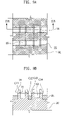
- FIG. 1 is a plan diagram illustrating a conventional finFET device.
- FIG. 2 is a cross-sectional diagram further illustrating the conventional finFET device, and taken along the line II-II in FIG. 1 .
- the finFET device is fabricated on a silicon substrate 8 that is covered with an insulating layer 7 .
- a vertically extended channel fin 3 is provided on the substrate 8 and is covered with a gate oxide layer 5 .
- Raised source/drain regions 1 and 2 are provided at both ends of the channel fin 3 on the substrate 8 .
- the source/drain regions 1 and 2 are connected by the channel fin 3 .
- a gate 6 is disposed between the source/drain regions 1 and 2 and extends across the channel fin 3 . Additionally, a gate spacer (not shown) may be formed on both sides of the gate 6 .
- the conventional finFET device described above may also have some drawbacks.
- the conventional finFET device may need complicated fabricating processes since, if a number of channels are formed, a corresponding number of source/drain regions are required. Complicated processes may increase the likelihood of errors.
- the shrinkage of pattern dimensions may require increased doping impurity concentrations. This may result in an increase of leakage current, and thereby device characteristics, such as refresh time, are degraded.
- Embodiments of the invention address these and other disadvantages of the conventional art.
- Some embodiments of the invention provide a finFET device that may effectively suppress leakage current.
- Other embodiments of the invention provide a simplified method of fabricating a finFET device that effectively suppresses leakage current.
- FIG. 1 is a plan diagram illustrating a conventional finFET device.
- FIG. 2 is a cross-sectional diagram taken along the line II-II of FIG. 1 .
- FIG. 3A through 10D illustrate a method of fabricating a finFET device and a resulting structure in accordance with some embodiments of the present invention.
- FIG. 3A is a plan diagram illustrating an initial structure including mask blocks on a semiconductor substrate.
- FIG. 3B is a cross-sectional diagram taken along the line IIIB-IIIB of FIG. 3A .
- FIG. 4 is a cross-sectional diagram illustrating a laterally etched nitride layer of the mask block.
- FIG. 5 is a cross-sectional diagram illustrating a spacer formed on sidewalls of the mask block.
- FIG. 6 is a cross-sectional diagram illustrating a trench formed in the substrate.
- FIG. 7 is a cross-sectional diagram illustrating the trench filled with a trench-insulating layer.
- FIG. 8A is a plan diagram illustrating a structure from which the mask blocks are removed.
- FIG. 8B is a cross-sectional diagram taken along the line VIIIB-VIIIB of FIG. 8A .
- FIG. 9A is a plan diagram illustrating a mask layer provided on a structure of FIG. 8A .
- FIG. 9B is a cross-sectional diagram taken along the line IXB-IXB of FIG. 9A .
- FIG. 10A is a plan diagram illustrating gate lines provided on a prior structure of FIG. 9A .
- FIG. 10B is a cross-sectional diagram taken along the line XB-XB of FIG. 10A .
- FIG. 10C is a cross-sectional diagram taken along the line XC-XC of FIG. 10A .
- FIG. 10D is a cross-sectional diagram taken along the line XD-XD of FIG. 10A .
- FIGS. 11 through 13 illustrate a method of fabricating a finFET device and a resulting structure in accordance with some other embodiments of the invention.
- FIGS. 3A through 10D illustrate a method of fabricating a finFET device and a resulting structure in accordance with some embodiments of the invention.
- FIGS. 3A and 3B show an initial structure provided on a semiconductor substrate.
- FIG. 3A is a plan diagram illustrating an initial structure
- FIG. 3B is a cross-sectional diagram taken along the line IIIB-IIIB of FIG. 3A .
- a nitride layer 22 and an anti-reflection coating layer 23 are deposited in sequence and patterned on the semiconductor substrate 20 .
- an oxide layer 21 may be interposed between the semiconductor substrate 20 and the nitride layer 22 so as to enhance adhesive strength.
- the anti-reflection coating layer 23 and the underlying nitride layer 22 form together a plurality of mask blocks B 1 , each of which has a rectangular flattened shape in a plan view and is laterally spaced apart from an adjacent mask blocks B 1 .
- the patterned nitride layer 22 is slightly etched in the lateral direction by using etchant such as phosphoric acid. This process effectively shrinks the width of a recess hole (H 2 in FIG. 9B ) as will be described later.
- the narrower recess hole will make it possible to reduce the distance between adjacent channel fins, thus allowing much smaller dimensions of circuit patterns.
- a resultant structure is completely coated with suitable insulating material, which is then subjected to an etch-back process. So, as shown in FIG. 5 , a spacer 24 is formed on sidewalls of each mask block B 1 .
- an exposed region of the semiconductor substrate 20 is then partially etched using both the mask block B 1 and the spacer 24 as an etch mask, so that a trench H 1 is formed in the exposed region of the substrate 20 .
- the trench H 1 may have a cross-sectional profile of a rectangle.
- the trench H 1 may alternatively have other cross-sectional profiles such as a reverse triangle (i.e., overturned triangle), a reverse trapezoid, or other geometric shapes.
- the trench H 1 is filled with insulating material such as oxide, so that a trench-insulating layer 25 is produced in the trench H 1 .
- Shallow trench isolation (STI) techniques that are well known in this art may be used to form and fill the trench H 1 .
- FIGS. 8A and 8B the mask blocks B 1 composed of the anti-reflective coating layer 23 and the nitride layer 22 are completely removed. As shown in FIGS. 8A and 8B , however, the spacer 24 and the oxide layer 21 still remain on the substrate 20 .
- This removal step may include removing upper parts of the spacer 24 as well as the anti-reflective coating layer 23 by a chemical mechanical polishing (CMP) process, and further, removing the nitride layer 22 by using etchant such as phosphoric acid.
- FIG. 8A is a plan diagram illustrating a resultant structure on the substrate 20
- FIG. 8B is a cross-sectional diagram taken along the line VIIIB-VIIIB of FIG. 8A .
- FIG. 9A is a plan diagram illustrating a mask layer provided on the above resultant structure in FIG. 8A
- FIG. 9B is a cross-sectional diagram taken along the line IXB-IXB of FIG. 9A .
- the mask layer M 1 is deposited over the structure and then patterned. Patterned lines of the mask layer M 1 are spaced apart from each other and are extended across the rectangular patterns of the oxide layer 21 . That is, the patterned lines of the mask layer M 1 cross over the remaining spacers 24 . Therefore, the spacers 24 and the oxide layer 21 are partly exposed between the patterned lines of the mask layer M 1 . While the mask layer M 1 and exposed portions of the spacers 24 are used together as an etch mask, the structure is subjected to an etch process. Therefore, exposed portions of the oxide layer 21 are removed, and further, underlying portions of the substrate 20 are partially removed, thus forming recess holes H 2 . Silicon recess techniques well known in this art may be used to form the recess holes H 2 . By etching, the trench-insulating layer 25 is also partially removed.
- each raised portion C 11 through C 14 may form channel fins, a pair of channel fins being located on the sides of each recess hole H 2 . Furthermore, each channel fin is located between the trench-insulating layer 25 and the recess hole H 2 .
- FIGS. 10A through 10D gate lines 26 are provided over a structure which was shown above in FIGS. 9A and 9B , covering the channel fins C 11 -C 14 .
- FIG. 10A is a plan diagram illustrating the gate lines 26 on the structure
- FIG. 10B is cross-sectional diagram taken along the line XB-XB of FIG. 10A
- FIG. 10C is a cross-sectional diagram taken along the line XC-XC of FIG. 10A
- FIG. 10D is a cross-sectional diagram taken along the line XD-XD of FIG. 10A .
- the gate lines 26 extend across the channel fins C 11 -C 14 , as is best shown in FIG. 10A .
- Each gate line 26 includes a gate dielectric layer, a gate electrode, and a stopper layer, which are stacked in sequence on the substrate 20 but for clarity are not illustrated separately.
- the gate electrode may be formed of conductive material such as copper, whereas the gate dielectric layer and the stopper layer may be formed of an insulating material such as oxide.
- source/drain regions Q 1 through Q 3 are formed at both ends of the channel fins C 11 -C 14 by doping an impurity, adjoining both sides of the gate lines 26 , as is best shown in FIGS. 10B and 10D . So the source/drain regions Q 1 -Q 3 are connected by the channel fins C 11 -C 14 .
- the source/drain regions Q 1 -Q 3 may alternatively have other profiles such as a shallow rectangle, for example.
- a resulting structure of the finFET device includes the semiconductor substrate 20 , the trench-insulating layer 25 , the gate lines 26 , and the source/drain regions Q 1 -Q 3 .
- the substrate 20 has the trench (H 1 in FIG. 6 ) that defines specific regions surrounded therewith and is filled with the trench-insulating layer 25 .
- the channel fins C 11 - 14 are formed along both sides of the specific regions of the substrate 20 .
- the gate lines 26 overlay and extend across the channel fins C 11 -C 14 .
- the source/drain regions Q 1 -Q 3 are formed at both ends of the channel fins C 11 -C 14 and also connected by the channel fins C 11 -C 14 .
- the channel fins C 11 -C 14 are formed in the semiconductor substrate 20 having the trench structure, and further, the trench structure can be provided using existing processes. Therefore, the embodiments provide a relatively simple fabrication process, and therefore the likelihood of process errors is reduced.
- the finFET device has a dual fin structure wherein the respective one in the pair of channel fins C 11 -C 14 is separated from the other in the pair by the gate dielectric layer provided in the recess hole H 2 . Additionally, the pairs of channel fins C 11 -C 12 , C 13 -C 14 connects together the source/drain regions Q 1 -Q 3 . To more effectively suppress unwanted leakage current between the adjacent channels, the bottom of the recess hole H 2 is positioned between the top and bottom of the trench-insulating layer 25 .
- FIGS. 11 through 13 illustrate a method of fabricating a finFET device and a resulting structure in accordance with other embodiments of the invention.
- an oxide layer 21 , a nitride layer 22 , and an anti-reflection coating layer 23 are deposited in sequence and patterned on a semiconductor substrate 30 . While the patterned layers 21 , 22 and 23 are used as an etch mask, an exposed region of the semiconductor substrate 30 is partially etched. Thus a trench H 3 is formed in the exposed region of the substrate 30 .
- the trench H 3 is filled with insulating material such as oxide, so a trench-insulating layer 35 is produced in the trench H 3 .
- the patterned layers 21 , 22 , and 23 are then removed, and a suitable fin mask pattern (not shown) is provided on the substrate 30 . With the fin mask pattern used, exposed portions of the substrate 30 are recessed by etching to form recess holes H 4 . By etching, the trench-insulating layer 35 is also partially removed.
- the fin mask pattern is removed, leaving raised portions C 21 , C 22 , C 23 , and C 24 on the substrate 30 .
- the raised portions C 21 -C 24 form channel fins, a pair of which is located along the sides of each recess hole H 4 .
- the channel fins C 21 -C 24 may have a cross-sectional profile shaped like a pointed triangle.
- the channel fins C 21 - 24 may have other cross-sectional profiles, for example, profiles that are shaped like a rectangle, a trapezoid, or some other geometric shape.
- gate lines 36 are provided over a resulting structure in FIG. 12 , covering the channel fins C 21 -C 24 . Subsequent processes are the same as those discussed above with respect to the embodiments illustrated in FIGS. 3-10 , and therefore a detailed discussion is omitted.
- a finFET device includes a semiconductor substrate having a trench formed therein to define a specific region surrounded with the trench; a trench-insulating layer filling the trench; at least one channel fin formed in the specific region; gate lines overlying and extending across the channel fin; and source/drain regions formed at both ends of the channel fin and connected by the channel fin.
- a method of fabricating a finFET device includes providing a semiconductor substrate having a specific region; forming a trench in the semiconductor substrate by etching such that the specific region is surrounded with the trench; forming a trench-insulating layer filling the trench; forming recess holes within the specific region such that channel fins are formed by raised portions of the semiconductor substrate on both sides of the recess holes; forming gate lines overlying and extending across the channel fins; and forming source/drain regions at both ends of the channel fins.
- a method of fabricating a finFET device includes providing a semiconductor substrate having a specific region; forming mask blocks on the semiconductor substrate such that the mask blocks cover the specific region; forming a spacer on sidewalls of the mask blocks; forming a trench in the semiconductor substrate by etching with the mask blocks used as an etch mask; forming a trench-insulating layer filling the trench; removing the mask blocks from the semiconductor substrate; forming mask lines on the semiconductor substrate such that the mask lines cross over the spacer; forming recess holes within the specific region by etching the semiconductor substrate with both the mask lines and the spacer used as an etch mask such that channel fins are formed by raised portions of the semiconductor substrate on both sides of the recess holes; removing both the mask lines and the spacer such that the channel fins are exposed; forming gate lines overlying and extending across the channel fins; and forming source/drain regions at both ends of the channel fins.
Abstract
A finFET device includes a semiconductor substrate having specific regions surrounded with a trench. The trench is filled with an insulating layer, and recess holes are formed within the specific regions such that channel fins are formed by raised portions of the semiconductor substrate on both sides of the recess holes. Gate lines are formed to overlie and extend across the channel fins. Source/drain regions are formed at both ends of the channel fins and connected by the channel fins. Other embodiments are described and claimed.
Description
This application claims priority from Korean Patent Application No. 2004-9606, filed Feb. 13, 2004, the content of which is incorporated by reference in its entirety for all purposes.
1. Field of the Invention
This disclosure relates generally to a semiconductor device and, more particularly, to a field effect transistor (FET) device having a fin-shaped channel and a method of fabricating the FET device.
2. Description of the Related Art
Along with advances in semiconductor technology, a semiconductor integrated circuit (IC) device becomes faster in operation and higher integrated. To continue performance enhancement of the device and reduction in leakage current, device design engineers have researched and developed a variety of new device structures available for sub-10 nm generations. One promising device structure is a field effect transistor device having a fin-shaped channel (finFET), such as the structure recently proposed by Chenming Hu et al. of the Regents of the University of California, USA.
This finFET device structure features a transistor channel that is formed on the vertical surfaces of an ultrathin Si fin and controlled by gate electrodes formed on both sides of the fin, and two gates that are self-aligned to each other and to the source/drain regions. Thus, this structure may also be referred to as a self-aligned double-gate finFET.
Referring to FIGS. 1 and 2 , the finFET device is fabricated on a silicon substrate 8 that is covered with an insulating layer 7. A vertically extended channel fin 3 is provided on the substrate 8 and is covered with a gate oxide layer 5. Raised source/ drain regions 1 and 2 are provided at both ends of the channel fin 3 on the substrate 8. The source/ drain regions 1 and 2 are connected by the channel fin 3. A gate 6 is disposed between the source/ drain regions 1 and 2 and extends across the channel fin 3. Additionally, a gate spacer (not shown) may be formed on both sides of the gate 6.
Unfortunately, the conventional finFET device described above may also have some drawbacks. For example, the conventional finFET device may need complicated fabricating processes since, if a number of channels are formed, a corresponding number of source/drain regions are required. Complicated processes may increase the likelihood of errors. Furthermore, the shrinkage of pattern dimensions may require increased doping impurity concentrations. This may result in an increase of leakage current, and thereby device characteristics, such as refresh time, are degraded.
Embodiments of the invention address these and other disadvantages of the conventional art.
Some embodiments of the invention provide a finFET device that may effectively suppress leakage current. Other embodiments of the invention provide a simplified method of fabricating a finFET device that effectively suppresses leakage current.
Exemplary, non-limiting embodiments of the invention will now be described more fully hereinafter with reference to the accompanying drawings. This invention may, however, be embodied in many different forms and should not be construed as limited to the exemplary embodiments set forth herein. Rather, the disclosed embodiments are provided so that this disclosure will be thorough and complete, and will fully convey the scope of the invention to those skilled in the art. The principles and feature of this invention may be employed in varied and numerous embodiments without departing from the scope of the invention.
In the description, well-known structures and processes have not been described or illustrated in detail to avoid obscuring the present invention. It will be appreciated that the figures are not drawn to scale. Rather, for simplicity and clarity of illustration, the dimensions of some of the elements are exaggerated relative to other elements. Like reference numerals and characters are used for like and corresponding parts of the various drawings.
Referring to FIGS. 3A and 3B , after a semiconductor substrate 20 made of silicon, for example, is provided, a nitride layer 22 and an anti-reflection coating layer 23 are deposited in sequence and patterned on the semiconductor substrate 20. In addition, an oxide layer 21 may be interposed between the semiconductor substrate 20 and the nitride layer 22 so as to enhance adhesive strength. The anti-reflection coating layer 23 and the underlying nitride layer 22 form together a plurality of mask blocks B1, each of which has a rectangular flattened shape in a plan view and is laterally spaced apart from an adjacent mask blocks B1.
Thereafter, as shown in FIG. 4 , the patterned nitride layer 22 is slightly etched in the lateral direction by using etchant such as phosphoric acid. This process effectively shrinks the width of a recess hole (H2 in FIG. 9B ) as will be described later. The narrower recess hole will make it possible to reduce the distance between adjacent channel fins, thus allowing much smaller dimensions of circuit patterns.
Next, a resultant structure is completely coated with suitable insulating material, which is then subjected to an etch-back process. So, as shown in FIG. 5 , a spacer 24 is formed on sidewalls of each mask block B1.
As shown in FIG. 6 , an exposed region of the semiconductor substrate 20 is then partially etched using both the mask block B1 and the spacer 24 as an etch mask, so that a trench H1 is formed in the exposed region of the substrate 20. As seen in FIG. 6 , the trench H1 may have a cross-sectional profile of a rectangle. However, the trench H1 may alternatively have other cross-sectional profiles such as a reverse triangle (i.e., overturned triangle), a reverse trapezoid, or other geometric shapes.
Next, as shown in FIG. 7 , the trench H1 is filled with insulating material such as oxide, so that a trench-insulating layer 25 is produced in the trench H1. Shallow trench isolation (STI) techniques that are well known in this art may be used to form and fill the trench H1.
After the trench-insulating layer 25 is formed, the mask blocks B1 composed of the anti-reflective coating layer 23 and the nitride layer 22 are completely removed. As shown in FIGS. 8A and 8B , however, the spacer 24 and the oxide layer 21 still remain on the substrate 20. This removal step may include removing upper parts of the spacer 24 as well as the anti-reflective coating layer 23 by a chemical mechanical polishing (CMP) process, and further, removing the nitride layer 22 by using etchant such as phosphoric acid. FIG. 8A is a plan diagram illustrating a resultant structure on the substrate 20, and FIG. 8B is a cross-sectional diagram taken along the line VIIIB-VIIIB of FIG. 8A .
Additionally, FIG. 9A is a plan diagram illustrating a mask layer provided on the above resultant structure in FIG. 8A , and FIG. 9B is a cross-sectional diagram taken along the line IXB-IXB of FIG. 9A .
Referring to FIGS. 9A and 9B , the mask layer M1 is deposited over the structure and then patterned. Patterned lines of the mask layer M1 are spaced apart from each other and are extended across the rectangular patterns of the oxide layer 21. That is, the patterned lines of the mask layer M1 cross over the remaining spacers 24. Therefore, the spacers 24 and the oxide layer 21 are partly exposed between the patterned lines of the mask layer M1. While the mask layer M1 and exposed portions of the spacers 24 are used together as an etch mask, the structure is subjected to an etch process. Therefore, exposed portions of the oxide layer 21 are removed, and further, underlying portions of the substrate 20 are partially removed, thus forming recess holes H2. Silicon recess techniques well known in this art may be used to form the recess holes H2. By etching, the trench-insulating layer 25 is also partially removed.
Thereafter, the mask layer M1, the spacers 24, and the oxide layer 21 are all removed, thus leaving raised portions C11, C12, C13, and C14 of the substrate 20. Each raised portion C11 through C14 may form channel fins, a pair of channel fins being located on the sides of each recess hole H2. Furthermore, each channel fin is located between the trench-insulating layer 25 and the recess hole H2.
Next, as shown in FIGS. 10A through 10D , gate lines 26 are provided over a structure which was shown above in FIGS. 9A and 9B , covering the channel fins C11-C14. FIG. 10A is a plan diagram illustrating the gate lines 26 on the structure, and FIG. 10B is cross-sectional diagram taken along the line XB-XB of FIG. 10A . Additionally, FIG. 10C is a cross-sectional diagram taken along the line XC-XC of FIG. 10A , and FIG. 10D is a cross-sectional diagram taken along the line XD-XD of FIG. 10A .
The gate lines 26 extend across the channel fins C11-C14, as is best shown in FIG. 10A . Each gate line 26 includes a gate dielectric layer, a gate electrode, and a stopper layer, which are stacked in sequence on the substrate 20 but for clarity are not illustrated separately. The gate electrode may be formed of conductive material such as copper, whereas the gate dielectric layer and the stopper layer may be formed of an insulating material such as oxide.
After the gate lines 26 are formed, source/drain regions Q1 through Q3 are formed at both ends of the channel fins C11-C14 by doping an impurity, adjoining both sides of the gate lines 26, as is best shown in FIGS. 10B and 10D . So the source/drain regions Q1-Q3 are connected by the channel fins C11-C14. Instead of the profile illustrated in FIG. 10D , the source/drain regions Q1-Q3 may alternatively have other profiles such as a shallow rectangle, for example.
Thereafter, a suitable insulating layer, a metal contact, a metal line, and so on are provided in sequence on the above structure. These processes are well known in this art, and therefore a detailed discussion is omitted.
As seen from FIGS. 10A-10D , a resulting structure of the finFET device according to these embodiments includes the semiconductor substrate 20, the trench-insulating layer 25, the gate lines 26, and the source/drain regions Q1-Q3. The substrate 20 has the trench (H1 in FIG. 6 ) that defines specific regions surrounded therewith and is filled with the trench-insulating layer 25. The channel fins C11-14 are formed along both sides of the specific regions of the substrate 20. The gate lines 26 overlay and extend across the channel fins C11-C14. The source/drain regions Q1-Q3 are formed at both ends of the channel fins C11-C14 and also connected by the channel fins C11-C14.
As discussed, the channel fins C11-C14 are formed in the semiconductor substrate 20 having the trench structure, and further, the trench structure can be provided using existing processes. Therefore, the embodiments provide a relatively simple fabrication process, and therefore the likelihood of process errors is reduced.
The finFET device according to the embodiments described above has a dual fin structure wherein the respective one in the pair of channel fins C11-C14 is separated from the other in the pair by the gate dielectric layer provided in the recess hole H2. Additionally, the pairs of channel fins C11-C12, C13-C14 connects together the source/drain regions Q1-Q3. To more effectively suppress unwanted leakage current between the adjacent channels, the bottom of the recess hole H2 is positioned between the top and bottom of the trench-insulating layer 25.
Referring to FIG. 11 , an oxide layer 21, a nitride layer 22, and an anti-reflection coating layer 23 are deposited in sequence and patterned on a semiconductor substrate 30. While the patterned layers 21, 22 and 23 are used as an etch mask, an exposed region of the semiconductor substrate 30 is partially etched. Thus a trench H3 is formed in the exposed region of the substrate 30.
Next, as shown in FIG. 12 , the trench H3 is filled with insulating material such as oxide, so a trench-insulating layer 35 is produced in the trench H3. The patterned layers 21, 22, and 23 are then removed, and a suitable fin mask pattern (not shown) is provided on the substrate 30. With the fin mask pattern used, exposed portions of the substrate 30 are recessed by etching to form recess holes H4. By etching, the trench-insulating layer 35 is also partially removed.
Next, the fin mask pattern is removed, leaving raised portions C21, C22, C23, and C24 on the substrate 30. The raised portions C21-C24 form channel fins, a pair of which is located along the sides of each recess hole H4. As illustrated in FIG. 12 , the channel fins C21-C24 may have a cross-sectional profile shaped like a pointed triangle. Alternatively, the channel fins C21-24 may have other cross-sectional profiles, for example, profiles that are shaped like a rectangle, a trapezoid, or some other geometric shape.
Next, as shown in FIG. 13 , gate lines 36 are provided over a resulting structure in FIG. 12 , covering the channel fins C21-C24. Subsequent processes are the same as those discussed above with respect to the embodiments illustrated in FIGS. 3-10 , and therefore a detailed discussion is omitted.
The invention may be practiced in many ways. Exemplary, non-limiting descriptions of some embodiments of the invention are described in the following paragraphs.
According to some embodiments of the invention, a finFET device includes a semiconductor substrate having a trench formed therein to define a specific region surrounded with the trench; a trench-insulating layer filling the trench; at least one channel fin formed in the specific region; gate lines overlying and extending across the channel fin; and source/drain regions formed at both ends of the channel fin and connected by the channel fin.
According to other embodiments of the invention, a method of fabricating a finFET device includes providing a semiconductor substrate having a specific region; forming a trench in the semiconductor substrate by etching such that the specific region is surrounded with the trench; forming a trench-insulating layer filling the trench; forming recess holes within the specific region such that channel fins are formed by raised portions of the semiconductor substrate on both sides of the recess holes; forming gate lines overlying and extending across the channel fins; and forming source/drain regions at both ends of the channel fins.
According to still other embodiments of the invention, a method of fabricating a finFET device includes providing a semiconductor substrate having a specific region; forming mask blocks on the semiconductor substrate such that the mask blocks cover the specific region; forming a spacer on sidewalls of the mask blocks; forming a trench in the semiconductor substrate by etching with the mask blocks used as an etch mask; forming a trench-insulating layer filling the trench; removing the mask blocks from the semiconductor substrate; forming mask lines on the semiconductor substrate such that the mask lines cross over the spacer; forming recess holes within the specific region by etching the semiconductor substrate with both the mask lines and the spacer used as an etch mask such that channel fins are formed by raised portions of the semiconductor substrate on both sides of the recess holes; removing both the mask lines and the spacer such that the channel fins are exposed; forming gate lines overlying and extending across the channel fins; and forming source/drain regions at both ends of the channel fins.
While this invention has been particularly shown and described with reference to exemplary embodiments thereof, it will be understood by those skilled in the art that various changes in form and details may be made therein without departing from the spirit and scope of the invention as defined by the appended claims.
Claims (8)
1. A field effect transistor (FET) device having a channel fin structure, comprising:
a semiconductor substrate having a trench formed therein to define a specific region surrounded by the trench;
a trench-insulating layer filling the trench;
a pair of channel fins formed in the specific region, each of the pair spaced apart by a recess hole having a bottom that is at a height above a bottom of the trench;
gate lines overlying and extending across the at least one channel fin; and
source/drain regions formed at both ends of the at least one channel fin and connected by the at least one channel fin.
2. The FET device of claim 1 , wherein the bottom of the recess hole is positioned below a top and above a bottom of the trench-insulating layer.
3. The FET device of claim 1 , wherein the recess hole is filled by one of the gate lines.
4. The FET device of claim 3 , wherein the recess hole does not include the trench-insulating layer.
5. The FET device of claim 1 , wherein the trench has a cross-sectional profile shaped like a reverse triangle or a reverse trapezoid.
6. The FET device of claim 1 , wherein the height of the trench-insulating layer is smaller than the depth of the trench.
7. The FET device of claim 1 , wherein at least one of the channel fins has a cross-sectional profile shaped like a pointed triangle or a trapezoid.
8. The FET device of claim 1 , wherein a bottom of the source/drain regions is positioned between a top and a bottom of the trench-insulating layer.
Priority Applications (1)
| Application Number | Priority Date | Filing Date | Title |
|---|---|---|---|
| US11/848,144 US20070293011A1 (en) | 2004-02-13 | 2007-08-30 | Field effect transistor device with channel fin structure and method of fabricating the same |
Applications Claiming Priority (2)
| Application Number | Priority Date | Filing Date | Title |
|---|---|---|---|
| KR2004-9606 | 2004-02-13 | ||
| KR1020040009606A KR100610496B1 (en) | 2004-02-13 | 2004-02-13 | Field Effect Transistor device with fin structure and method for manufacturing thereof |
Related Child Applications (1)
| Application Number | Title | Priority Date | Filing Date |
|---|---|---|---|
| US11/848,144 Division US20070293011A1 (en) | 2004-02-13 | 2007-08-30 | Field effect transistor device with channel fin structure and method of fabricating the same |
Publications (2)
| Publication Number | Publication Date |
|---|---|
| US20050179030A1 US20050179030A1 (en) | 2005-08-18 |
| US7279774B2 true US7279774B2 (en) | 2007-10-09 |
Family
ID=34836732
Family Applications (2)
| Application Number | Title | Priority Date | Filing Date |
|---|---|---|---|
| US10/938,436 Expired - Fee Related US7279774B2 (en) | 2004-02-13 | 2004-09-09 | Bulk substrates in FinFETs with trench insulation surrounding FIN pairs having FINs separated by recess hole shallower than trench |
| US11/848,144 Abandoned US20070293011A1 (en) | 2004-02-13 | 2007-08-30 | Field effect transistor device with channel fin structure and method of fabricating the same |
Family Applications After (1)
| Application Number | Title | Priority Date | Filing Date |
|---|---|---|---|
| US11/848,144 Abandoned US20070293011A1 (en) | 2004-02-13 | 2007-08-30 | Field effect transistor device with channel fin structure and method of fabricating the same |
Country Status (2)
| Country | Link |
|---|---|
| US (2) | US7279774B2 (en) |
| KR (1) | KR100610496B1 (en) |
Cited By (12)
| Publication number | Priority date | Publication date | Assignee | Title |
|---|---|---|---|---|
| US20080079040A1 (en) * | 2006-09-29 | 2008-04-03 | Hynix Semiconductor Inc. | Transistor And Method For Manufacturing The Same |
| US20100252886A1 (en) * | 2006-08-22 | 2010-10-07 | Micron Technology, Inc. | Fin structures and methods of fabricating fin structures |
| CN104025293A (en) * | 2011-10-18 | 2014-09-03 | 英特尔公司 | Antifuse element utilizing non-planar topology |
| USRE45165E1 (en) * | 2005-07-29 | 2014-09-30 | Taiwan Semiconductor Manufacturing Company, Ltd. | Structure for a multiple-gate FET device and a method for its fabrication |
| US8890262B2 (en) | 2012-11-29 | 2014-11-18 | Globalfoundries Inc. | Semiconductor device having a metal gate recess |
| US8940602B2 (en) | 2013-04-11 | 2015-01-27 | International Business Machines Corporation | Self-aligned structure for bulk FinFET |
| US9034700B1 (en) | 2013-11-21 | 2015-05-19 | Samsung Electronics Co., Ltd. | Integrated circuit devices including finFETs and methods of forming the same |
| US9443852B2 (en) | 2014-02-19 | 2016-09-13 | Samsung Electronics Co., Ltd. | Integrated circuit devices with source/drain regions including multiple segments |
| US9559191B2 (en) | 2014-04-16 | 2017-01-31 | International Business Machines Corporation | Punch through stopper in bulk finFET device |
| US9805991B2 (en) | 2015-08-20 | 2017-10-31 | International Business Machines Corporation | Strained finFET device fabrication |
| US9905480B1 (en) * | 2016-11-15 | 2018-02-27 | Nuvoton Technology Corporation | Semiconductor devices and methods for forming the same |
| US11017999B2 (en) | 2016-10-05 | 2021-05-25 | International Business Machines Corporation | Method and structure for forming bulk FinFET with uniform channel height |
Families Citing this family (18)
| Publication number | Priority date | Publication date | Assignee | Title |
|---|---|---|---|---|
| KR100614800B1 (en) * | 2004-12-10 | 2006-08-22 | 삼성전자주식회사 | Method of fabricating a Fin Field Effect Transistor having a plurality of protrudent channels |
| KR100714285B1 (en) * | 2004-12-28 | 2007-05-02 | 주식회사 하이닉스반도체 | Semiconductor device and method for fabricating the same |
| KR100657969B1 (en) * | 2005-08-30 | 2006-12-14 | 삼성전자주식회사 | Method of fabricating a semiconductor device having a single gate electrode corresponding a pair of fin-type channel regions |
| US7928005B2 (en) * | 2005-09-27 | 2011-04-19 | Advanced Micro Devices, Inc. | Method for forming narrow structures in a semiconductor device |
| KR100675290B1 (en) * | 2005-11-24 | 2007-01-29 | 삼성전자주식회사 | Method of fabricating semiconductor devices having mcfet/finfet and related device |
| KR100683867B1 (en) | 2006-02-09 | 2007-02-15 | 삼성전자주식회사 | Semiconductor devices and methods of forming the same |
| KR100767399B1 (en) * | 2006-07-03 | 2007-10-17 | 삼성전자주식회사 | Method of fabricating semiconductor device having fin-fet |
| US7795096B2 (en) * | 2006-12-29 | 2010-09-14 | Qimonda Ag | Method of forming an integrated circuit with two types of transistors |
| KR100855870B1 (en) * | 2007-01-31 | 2008-09-03 | 재단법인서울대학교산학협력재단 | Firefet and fabricating method of the same |
| US7879659B2 (en) | 2007-07-17 | 2011-02-01 | Micron Technology, Inc. | Methods of fabricating semiconductor devices including dual fin structures |
| US7902057B2 (en) * | 2007-07-31 | 2011-03-08 | Micron Technology, Inc. | Methods of fabricating dual fin structures |
| US20090108353A1 (en) * | 2007-10-31 | 2009-04-30 | Advanced Micro Devices, Inc. | Finfet structure and methods |
| KR101205037B1 (en) * | 2011-02-28 | 2012-11-26 | 에스케이하이닉스 주식회사 | Semiconductor device and method for fabricating the same |
| KR101994079B1 (en) * | 2012-10-10 | 2019-09-30 | 삼성전자 주식회사 | Semiconductor device and fabricated method thereof |
| KR102291571B1 (en) * | 2015-01-13 | 2021-08-18 | 삼성전자주식회사 | Semiconductor device and the fabricating method thereof |
| US10121675B2 (en) * | 2016-12-29 | 2018-11-06 | Taiwan Semiconductor Manufacturing Co., Ltd | Semiconductor device and a method for fabricating the same |
| EP3404721A1 (en) * | 2017-05-15 | 2018-11-21 | IMEC vzw | A method for forming pillars in a vertical transistor device |
| KR102460847B1 (en) * | 2018-05-25 | 2022-10-28 | 삼성전자주식회사 | Semiconductor device and method for fabricating the same |
Citations (12)
| Publication number | Priority date | Publication date | Assignee | Title |
|---|---|---|---|---|
| JPS6394668A (en) | 1986-10-09 | 1988-04-25 | Sony Corp | Storage device |
| US5998845A (en) * | 1996-12-23 | 1999-12-07 | U.S. Philips Corporation | Semiconductor device having increased safe operating range |
| KR20010075236A (en) | 1998-09-25 | 2001-08-09 | 마이클 골위저, 호레스트 쉐퍼 | Integrated circuit comprising vertical transistors, and a method for the production thereof |
| KR20020018059A (en) | 2000-08-28 | 2002-03-07 | 다니구찌 이찌로오, 기타오카 다카시 | Mos semiconductor device and method of manufacturing the same |
| US6413802B1 (en) | 2000-10-23 | 2002-07-02 | The Regents Of The University Of California | Finfet transistor structures having a double gate channel extending vertically from a substrate and methods of manufacture |
| KR20030065631A (en) | 2002-01-30 | 2003-08-09 | 한국과학기술원 | Double-Gate FinFET |
| US6642090B1 (en) * | 2002-06-03 | 2003-11-04 | International Business Machines Corporation | Fin FET devices from bulk semiconductor and method for forming |
| US20040110331A1 (en) * | 2002-12-06 | 2004-06-10 | Yee-Chia Yeo | CMOS inverters configured using multiple-gate transistors |
| US20050035415A1 (en) * | 2003-08-13 | 2005-02-17 | Yee-Chia Yeo | Multiple-gate transistors formed on bulk substrates |
| US6914277B1 (en) * | 2003-10-01 | 2005-07-05 | Advanced Micro Devices, Inc. | Merged FinFET P-channel/N-channel pair |
| US6963104B2 (en) * | 2003-06-12 | 2005-11-08 | Advanced Micro Devices, Inc. | Non-volatile memory device |
| US6989308B2 (en) * | 2004-03-11 | 2006-01-24 | International Business Machines Corporation | Method of forming FinFET gates without long etches |
Family Cites Families (1)
| Publication number | Priority date | Publication date | Assignee | Title |
|---|---|---|---|---|
| US7285466B2 (en) * | 2003-08-05 | 2007-10-23 | Samsung Electronics Co., Ltd. | Methods of forming metal oxide semiconductor (MOS) transistors having three dimensional channels |
-
2004
- 2004-02-13 KR KR1020040009606A patent/KR100610496B1/en not_active IP Right Cessation
- 2004-09-09 US US10/938,436 patent/US7279774B2/en not_active Expired - Fee Related
-
2007
- 2007-08-30 US US11/848,144 patent/US20070293011A1/en not_active Abandoned
Patent Citations (14)
| Publication number | Priority date | Publication date | Assignee | Title |
|---|---|---|---|---|
| JPS6394668A (en) | 1986-10-09 | 1988-04-25 | Sony Corp | Storage device |
| US5998845A (en) * | 1996-12-23 | 1999-12-07 | U.S. Philips Corporation | Semiconductor device having increased safe operating range |
| US6750095B1 (en) * | 1998-09-25 | 2004-06-15 | Infineon Technologies Ag | Integrated circuit with vertical transistors |
| KR20010075236A (en) | 1998-09-25 | 2001-08-09 | 마이클 골위저, 호레스트 쉐퍼 | Integrated circuit comprising vertical transistors, and a method for the production thereof |
| KR20020018059A (en) | 2000-08-28 | 2002-03-07 | 다니구찌 이찌로오, 기타오카 다카시 | Mos semiconductor device and method of manufacturing the same |
| US6548859B2 (en) * | 2000-08-28 | 2003-04-15 | Mitsubishi Denki Kabushiki Kaisha | MOS semiconductor device and method of manufacturing the same |
| US6413802B1 (en) | 2000-10-23 | 2002-07-02 | The Regents Of The University Of California | Finfet transistor structures having a double gate channel extending vertically from a substrate and methods of manufacture |
| KR20030065631A (en) | 2002-01-30 | 2003-08-09 | 한국과학기술원 | Double-Gate FinFET |
| US6642090B1 (en) * | 2002-06-03 | 2003-11-04 | International Business Machines Corporation | Fin FET devices from bulk semiconductor and method for forming |
| US20040110331A1 (en) * | 2002-12-06 | 2004-06-10 | Yee-Chia Yeo | CMOS inverters configured using multiple-gate transistors |
| US6963104B2 (en) * | 2003-06-12 | 2005-11-08 | Advanced Micro Devices, Inc. | Non-volatile memory device |
| US20050035415A1 (en) * | 2003-08-13 | 2005-02-17 | Yee-Chia Yeo | Multiple-gate transistors formed on bulk substrates |
| US6914277B1 (en) * | 2003-10-01 | 2005-07-05 | Advanced Micro Devices, Inc. | Merged FinFET P-channel/N-channel pair |
| US6989308B2 (en) * | 2004-03-11 | 2006-01-24 | International Business Machines Corporation | Method of forming FinFET gates without long etches |
Non-Patent Citations (4)
| Title |
|---|
| English language abstract of Japanese Publication No. 63-094668, Apr. 25, 1988. |
| English language abstract of Korean Publication No. 2001-0075236, Aug. 9, 2001. |
| English language abstract of Korean Publication No. 2002-0018059, Mar. 7, 2002. |
| English language abstract of Korean Publication No. 2003-0065631, Aug. 9, 2003. |
Cited By (25)
| Publication number | Priority date | Publication date | Assignee | Title |
|---|---|---|---|---|
| USRE45165E1 (en) * | 2005-07-29 | 2014-09-30 | Taiwan Semiconductor Manufacturing Company, Ltd. | Structure for a multiple-gate FET device and a method for its fabrication |
| USRE45944E1 (en) | 2005-07-29 | 2016-03-22 | Taiwan Semiconductor Manufacturing Company, Ltd. | Structure for a multiple-gate FET device and a method for its fabrication |
| US9281402B2 (en) | 2006-08-22 | 2016-03-08 | Micron Technology, Inc. | Methods of fabricating fin structures |
| US20100252886A1 (en) * | 2006-08-22 | 2010-10-07 | Micron Technology, Inc. | Fin structures and methods of fabricating fin structures |
| US8076721B2 (en) | 2006-08-22 | 2011-12-13 | Micron Technology, Inc. | Fin structures and methods of fabricating fin structures |
| US8748280B2 (en) | 2006-08-22 | 2014-06-10 | Micron Technology, Inc. | Methods of fabricating fin structures |
| US20080079040A1 (en) * | 2006-09-29 | 2008-04-03 | Hynix Semiconductor Inc. | Transistor And Method For Manufacturing The Same |
| CN104025293A (en) * | 2011-10-18 | 2014-09-03 | 英特尔公司 | Antifuse element utilizing non-planar topology |
| US8890262B2 (en) | 2012-11-29 | 2014-11-18 | Globalfoundries Inc. | Semiconductor device having a metal gate recess |
| US9466676B2 (en) | 2012-11-29 | 2016-10-11 | Globalfoundries Inc. | Method for forming a semiconductor device having a metal gate recess |
| US8940602B2 (en) | 2013-04-11 | 2015-01-27 | International Business Machines Corporation | Self-aligned structure for bulk FinFET |
| US9263521B2 (en) | 2013-11-21 | 2016-02-16 | Samsung Electronics Co., Ltd. | Integrated circuit devices including finFETs and methods of forming the same |
| US9034700B1 (en) | 2013-11-21 | 2015-05-19 | Samsung Electronics Co., Ltd. | Integrated circuit devices including finFETs and methods of forming the same |
| US9443852B2 (en) | 2014-02-19 | 2016-09-13 | Samsung Electronics Co., Ltd. | Integrated circuit devices with source/drain regions including multiple segments |
| US9559191B2 (en) | 2014-04-16 | 2017-01-31 | International Business Machines Corporation | Punch through stopper in bulk finFET device |
| US10084070B2 (en) | 2014-04-16 | 2018-09-25 | International Business Machines Corporation | Punch through stopper in bulk finFET device |
| US10103251B2 (en) | 2014-04-16 | 2018-10-16 | International Business Machines Corporation | Punch through stopper in bulk finFET device |
| US10109723B2 (en) | 2014-04-16 | 2018-10-23 | International Business Machines Corporation | Punch through stopper in bulk FinFET device |
| US10170594B2 (en) | 2014-04-16 | 2019-01-01 | International Business Machines Corporation | Punch through stopper in bulk finFET device |
| US10224420B2 (en) | 2014-04-16 | 2019-03-05 | International Business Machines Corporation | Punch through stopper in bulk finFET device |
| US10629709B2 (en) | 2014-04-16 | 2020-04-21 | Tessera, Inc. | Punch through stopper in bulk finFET device |
| US11404560B2 (en) | 2014-04-16 | 2022-08-02 | Tessera Llc | Punch through stopper in bulk finFET device |
| US9805991B2 (en) | 2015-08-20 | 2017-10-31 | International Business Machines Corporation | Strained finFET device fabrication |
| US11017999B2 (en) | 2016-10-05 | 2021-05-25 | International Business Machines Corporation | Method and structure for forming bulk FinFET with uniform channel height |
| US9905480B1 (en) * | 2016-11-15 | 2018-02-27 | Nuvoton Technology Corporation | Semiconductor devices and methods for forming the same |
Also Published As
| Publication number | Publication date |
|---|---|
| US20070293011A1 (en) | 2007-12-20 |
| KR100610496B1 (en) | 2006-08-09 |
| KR20050081389A (en) | 2005-08-19 |
| US20050179030A1 (en) | 2005-08-18 |
Similar Documents
| Publication | Publication Date | Title |
|---|---|---|
| US7279774B2 (en) | Bulk substrates in FinFETs with trench insulation surrounding FIN pairs having FINs separated by recess hole shallower than trench | |
| KR100618900B1 (en) | Mos field effect transistor having a plurality of channels and method of fabricating the same | |
| US7470588B2 (en) | Transistors including laterally extended active regions and methods of fabricating the same | |
| US7396726B2 (en) | Methods of fabricating surrounded-channel transistors with directionally etched gate or insulator formation regions | |
| US7470951B2 (en) | Hybrid-FET and its application as SRAM | |
| TWI509736B (en) | Finfets having dielectric punch-through stoppers | |
| US9196540B2 (en) | FinFET structure with novel edge fins | |
| US8373223B2 (en) | Semiconductor device and method for fabricating the same | |
| US8410547B2 (en) | Semiconductor device and method for fabricating the same | |
| US7285456B2 (en) | Method of fabricating a fin field effect transistor having a plurality of protruding channels | |
| KR20230118785A (en) | A semiconductor device | |
| KR100763337B1 (en) | Semiconductor device having buried gate line and method of fabricating the same | |
| US7508048B2 (en) | Methods of fabricating a semiconductor device having multi-gate insulation layers and semiconductor devices fabricated thereby | |
| KR20070063203A (en) | Isolation method defining active fins, method for fabricating semiconductor device using the same, and semiconductor device fabricated thereby | |
| CN113782515A (en) | Integrated circuit device and method of manufacturing an integrated circuit device | |
| KR100618904B1 (en) | Semiconductor device having finfet and method of forming the same | |
| US10410886B2 (en) | Methods of fabricating a semiconductor device | |
| CN112201692A (en) | Fully-enclosed grid fin field effect transistor and manufacturing method thereof | |
| US20160380081A1 (en) | Finfet and method of fabricating the same | |
| KR101959388B1 (en) | Semiconductor device and method of fabricating the same | |
| JP2010118410A (en) | Semiconductor device | |
| US20210257491A1 (en) | Multi-gate semiconductor structure and method of manufacturing the same | |
| US20080061363A1 (en) | Integrated transistor device and corresponding manufacturing method | |
| KR100683491B1 (en) | Method for fabricating semiconductor device | |
| CN105448968B (en) | Method for manufacturing fin field effect transistor |
Legal Events
| Date | Code | Title | Description |
|---|---|---|---|
| AS | Assignment |
Owner name: SAMSUNG ELECTRONICS CO., LTD., KOREA, REPUBLIC OF Free format text: ASSIGNMENT OF ASSIGNORS INTEREST;ASSIGNORS:SEO, HYEOUNG-WON;YANG, WOUN-SUCK;SONG, DU-HEON;AND OTHERS;REEL/FRAME:015415/0447;SIGNING DATES FROM 20040825 TO 20040827 |
|
| FEPP | Fee payment procedure |
Free format text: PAYOR NUMBER ASSIGNED (ORIGINAL EVENT CODE: ASPN); ENTITY STATUS OF PATENT OWNER: LARGE ENTITY |
|
| CC | Certificate of correction | ||
| FPAY | Fee payment |
Year of fee payment: 4 |
|
| REMI | Maintenance fee reminder mailed | ||
| LAPS | Lapse for failure to pay maintenance fees | ||
| STCH | Information on status: patent discontinuation |
Free format text: PATENT EXPIRED DUE TO NONPAYMENT OF MAINTENANCE FEES UNDER 37 CFR 1.362 |
|
| FP | Lapsed due to failure to pay maintenance fee |
Effective date: 20151009 |