US7273822B2 - Methods and apparatus for forming thin films for semiconductor devices - Google Patents
Methods and apparatus for forming thin films for semiconductor devices Download PDFInfo
- Publication number
- US7273822B2 US7273822B2 US11/038,324 US3832405A US7273822B2 US 7273822 B2 US7273822 B2 US 7273822B2 US 3832405 A US3832405 A US 3832405A US 7273822 B2 US7273822 B2 US 7273822B2
- Authority
- US
- United States
- Prior art keywords
- thin film
- gas
- reactant
- chamber
- heater
- Prior art date
- Legal status (The legal status is an assumption and is not a legal conclusion. Google has not performed a legal analysis and makes no representation as to the accuracy of the status listed.)
- Active, expires
Links
- 239000010409 thin film Substances 0.000 title claims abstract description 129
- 238000000034 method Methods 0.000 title claims abstract description 119
- 239000004065 semiconductor Substances 0.000 title claims abstract description 26
- 239000000376 reactant Substances 0.000 claims abstract description 130
- 239000000758 substrate Substances 0.000 claims abstract description 54
- 238000010926 purge Methods 0.000 claims abstract description 50
- 239000000126 substance Substances 0.000 claims abstract description 12
- 238000006073 displacement reaction Methods 0.000 claims abstract description 8
- 239000007789 gas Substances 0.000 claims description 195
- 238000010438 heat treatment Methods 0.000 claims description 42
- 239000010408 film Substances 0.000 claims description 20
- 239000012495 reaction gas Substances 0.000 claims description 15
- PJXISJQVUVHSOJ-UHFFFAOYSA-N indium(III) oxide Inorganic materials [O-2].[O-2].[O-2].[In+3].[In+3] PJXISJQVUVHSOJ-UHFFFAOYSA-N 0.000 claims description 13
- 150000004767 nitrides Chemical class 0.000 claims description 12
- MCMNRKCIXSYSNV-UHFFFAOYSA-N Zirconium dioxide Chemical compound O=[Zr]=O MCMNRKCIXSYSNV-UHFFFAOYSA-N 0.000 claims description 8
- 239000011261 inert gas Substances 0.000 claims description 8
- ZKATWMILCYLAPD-UHFFFAOYSA-N niobium pentoxide Chemical compound O=[Nb](=O)O[Nb](=O)=O ZKATWMILCYLAPD-UHFFFAOYSA-N 0.000 claims description 8
- 238000005086 pumping Methods 0.000 claims description 8
- WOCIAKWEIIZHES-UHFFFAOYSA-N ruthenium(iv) oxide Chemical compound O=[Ru]=O WOCIAKWEIIZHES-UHFFFAOYSA-N 0.000 claims description 8
- 229910052719 titanium Inorganic materials 0.000 claims description 6
- PNEYBMLMFCGWSK-UHFFFAOYSA-N aluminium oxide Inorganic materials [O-2].[O-2].[O-2].[Al+3].[Al+3] PNEYBMLMFCGWSK-UHFFFAOYSA-N 0.000 claims description 4
- CETPSERCERDGAM-UHFFFAOYSA-N ceric oxide Chemical compound O=[Ce]=O CETPSERCERDGAM-UHFFFAOYSA-N 0.000 claims description 4
- 229910000422 cerium(IV) oxide Inorganic materials 0.000 claims description 4
- 229910052593 corundum Inorganic materials 0.000 claims description 4
- HTXDPTMKBJXEOW-UHFFFAOYSA-N iridium(IV) oxide Inorganic materials O=[Ir]=O HTXDPTMKBJXEOW-UHFFFAOYSA-N 0.000 claims description 4
- 239000003446 ligand Substances 0.000 claims description 4
- PBCFLUZVCVVTBY-UHFFFAOYSA-N tantalum pentoxide Inorganic materials O=[Ta](=O)O[Ta](=O)=O PBCFLUZVCVVTBY-UHFFFAOYSA-N 0.000 claims description 4
- 229910001845 yogo sapphire Inorganic materials 0.000 claims description 4
- 102100032047 Alsin Human genes 0.000 claims description 3
- 101710187109 Alsin Proteins 0.000 claims description 3
- -1 CaRuO3 Inorganic materials 0.000 claims description 3
- 229910020294 Pb(Zr,Ti)O3 Inorganic materials 0.000 claims description 3
- 229910003781 PbTiO3 Inorganic materials 0.000 claims description 3
- 229910002353 SrRuO3 Inorganic materials 0.000 claims description 3
- 229910002370 SrTiO3 Inorganic materials 0.000 claims description 3
- 229910004200 TaSiN Inorganic materials 0.000 claims description 3
- 229910008482 TiSiN Inorganic materials 0.000 claims description 3
- ATJFFYVFTNAWJD-UHFFFAOYSA-N Tin Chemical compound [Sn] ATJFFYVFTNAWJD-UHFFFAOYSA-N 0.000 claims description 3
- 229910008807 WSiN Inorganic materials 0.000 claims description 3
- 229910052782 aluminium Inorganic materials 0.000 claims description 3
- 229910052802 copper Inorganic materials 0.000 claims description 3
- CJNBYAVZURUTKZ-UHFFFAOYSA-N hafnium(IV) oxide Inorganic materials O=[Hf]=O CJNBYAVZURUTKZ-UHFFFAOYSA-N 0.000 claims description 3
- 229910052741 iridium Inorganic materials 0.000 claims description 3
- QRXWMOHMRWLFEY-UHFFFAOYSA-N isoniazide Chemical compound NNC(=O)C1=CC=NC=C1 QRXWMOHMRWLFEY-UHFFFAOYSA-N 0.000 claims description 3
- 229910052746 lanthanum Inorganic materials 0.000 claims description 3
- 229910052750 molybdenum Inorganic materials 0.000 claims description 3
- 229910052697 platinum Inorganic materials 0.000 claims description 3
- 229910052703 rhodium Inorganic materials 0.000 claims description 3
- 229910052707 ruthenium Inorganic materials 0.000 claims description 3
- 229910052709 silver Inorganic materials 0.000 claims description 3
- 229910052715 tantalum Inorganic materials 0.000 claims description 3
- 229910052721 tungsten Inorganic materials 0.000 claims description 3
- 229910002938 (Ba,Sr)TiO3 Inorganic materials 0.000 claims 2
- 239000000470 constituent Substances 0.000 abstract description 5
- XKRFYHLGVUSROY-UHFFFAOYSA-N Argon Chemical compound [Ar] XKRFYHLGVUSROY-UHFFFAOYSA-N 0.000 description 22
- 238000000231 atomic layer deposition Methods 0.000 description 13
- 229910052786 argon Inorganic materials 0.000 description 11
- 238000005229 chemical vapour deposition Methods 0.000 description 11
- 239000000463 material Substances 0.000 description 9
- 239000007788 liquid Substances 0.000 description 7
- 230000000694 effects Effects 0.000 description 6
- IJGRMHOSHXDMSA-UHFFFAOYSA-N Atomic nitrogen Chemical compound N#N IJGRMHOSHXDMSA-UHFFFAOYSA-N 0.000 description 4
- GWEVSGVZZGPLCZ-UHFFFAOYSA-N Titan oxide Chemical compound O=[Ti]=O GWEVSGVZZGPLCZ-UHFFFAOYSA-N 0.000 description 4
- 150000001875 compounds Chemical class 0.000 description 4
- 229910001873 dinitrogen Inorganic materials 0.000 description 4
- 239000012535 impurity Substances 0.000 description 4
- 238000006243 chemical reaction Methods 0.000 description 3
- NFHFRUOZVGFOOS-UHFFFAOYSA-N palladium;triphenylphosphane Chemical compound [Pd].C1=CC=CC=C1P(C=1C=CC=CC=1)C1=CC=CC=C1.C1=CC=CC=C1P(C=1C=CC=CC=1)C1=CC=CC=C1.C1=CC=CC=C1P(C=1C=CC=CC=1)C1=CC=CC=C1.C1=CC=CC=C1P(C=1C=CC=CC=1)C1=CC=CC=C1 NFHFRUOZVGFOOS-UHFFFAOYSA-N 0.000 description 3
- 239000002356 single layer Substances 0.000 description 3
- 238000007796 conventional method Methods 0.000 description 2
- 125000004122 cyclic group Chemical group 0.000 description 2
- 239000003989 dielectric material Substances 0.000 description 2
- 229910000449 hafnium oxide Inorganic materials 0.000 description 2
- 239000010410 layer Substances 0.000 description 2
- 229910052751 metal Inorganic materials 0.000 description 2
- 239000002184 metal Substances 0.000 description 2
- 238000012986 modification Methods 0.000 description 2
- 230000004048 modification Effects 0.000 description 2
- 239000002245 particle Substances 0.000 description 2
- 238000005240 physical vapour deposition Methods 0.000 description 2
- 239000002243 precursor Substances 0.000 description 2
- 239000010936 titanium Substances 0.000 description 2
- VOITXYVAKOUIBA-UHFFFAOYSA-N triethylaluminium Chemical compound CC[Al](CC)CC VOITXYVAKOUIBA-UHFFFAOYSA-N 0.000 description 2
- JLTRXTDYQLMHGR-UHFFFAOYSA-N trimethylaluminium Chemical compound C[Al](C)C JLTRXTDYQLMHGR-UHFFFAOYSA-N 0.000 description 2
- WQKWNXSKQLVRHK-UHFFFAOYSA-N CC[Hf](C)N Chemical compound CC[Hf](C)N WQKWNXSKQLVRHK-UHFFFAOYSA-N 0.000 description 1
- QRDJMFAGNINQFN-UHFFFAOYSA-N CC[Ti](N)CC Chemical compound CC[Ti](N)CC QRDJMFAGNINQFN-UHFFFAOYSA-N 0.000 description 1
- QDGMSMUNXGCWRA-UHFFFAOYSA-N C[Ti](C)N Chemical compound C[Ti](C)N QDGMSMUNXGCWRA-UHFFFAOYSA-N 0.000 description 1
- 229910003074 TiCl4 Inorganic materials 0.000 description 1
- 229910010252 TiO3 Inorganic materials 0.000 description 1
- 230000003213 activating effect Effects 0.000 description 1
- 230000015572 biosynthetic process Effects 0.000 description 1
- 239000004020 conductor Substances 0.000 description 1
- 238000000354 decomposition reaction Methods 0.000 description 1
- 230000007547 defect Effects 0.000 description 1
- 238000005137 deposition process Methods 0.000 description 1
- 238000005516 engineering process Methods 0.000 description 1
- 238000002474 experimental method Methods 0.000 description 1
- 229910052735 hafnium Inorganic materials 0.000 description 1
- 150000004820 halides Chemical class 0.000 description 1
- 125000002887 hydroxy group Chemical group [H]O* 0.000 description 1
- 229910052745 lead Inorganic materials 0.000 description 1
- 239000004973 liquid crystal related substance Substances 0.000 description 1
- 238000004519 manufacturing process Methods 0.000 description 1
- 229910001507 metal halide Inorganic materials 0.000 description 1
- 150000005309 metal halides Chemical class 0.000 description 1
- 239000013110 organic ligand Substances 0.000 description 1
- 239000007800 oxidant agent Substances 0.000 description 1
- XJDNKRIXUMDJCW-UHFFFAOYSA-J titanium tetrachloride Chemical compound Cl[Ti](Cl)(Cl)Cl XJDNKRIXUMDJCW-UHFFFAOYSA-J 0.000 description 1
Images


Classifications
-
- H—ELECTRICITY
- H01—ELECTRIC ELEMENTS
- H01L—SEMICONDUCTOR DEVICES NOT COVERED BY CLASS H10
- H01L21/00—Processes or apparatus adapted for the manufacture or treatment of semiconductor or solid state devices or of parts thereof
- H01L21/02—Manufacture or treatment of semiconductor devices or of parts thereof
- H01L21/04—Manufacture or treatment of semiconductor devices or of parts thereof the devices having at least one potential-jump barrier or surface barrier, e.g. PN junction, depletion layer or carrier concentration layer
- H01L21/18—Manufacture or treatment of semiconductor devices or of parts thereof the devices having at least one potential-jump barrier or surface barrier, e.g. PN junction, depletion layer or carrier concentration layer the devices having semiconductor bodies comprising elements of Group IV of the Periodic System or AIIIBV compounds with or without impurities, e.g. doping materials
- H01L21/28—Manufacture of electrodes on semiconductor bodies using processes or apparatus not provided for in groups H01L21/20 - H01L21/268
- H01L21/283—Deposition of conductive or insulating materials for electrodes conducting electric current
- H01L21/285—Deposition of conductive or insulating materials for electrodes conducting electric current from a gas or vapour, e.g. condensation
- H01L21/28506—Deposition of conductive or insulating materials for electrodes conducting electric current from a gas or vapour, e.g. condensation of conductive layers
- H01L21/28512—Deposition of conductive or insulating materials for electrodes conducting electric current from a gas or vapour, e.g. condensation of conductive layers on semiconductor bodies comprising elements of Group IV of the Periodic System
- H01L21/28556—Deposition of conductive or insulating materials for electrodes conducting electric current from a gas or vapour, e.g. condensation of conductive layers on semiconductor bodies comprising elements of Group IV of the Periodic System by chemical means, e.g. CVD, LPCVD, PECVD, laser CVD
- H01L21/28562—Selective deposition
-
- C—CHEMISTRY; METALLURGY
- C23—COATING METALLIC MATERIAL; COATING MATERIAL WITH METALLIC MATERIAL; CHEMICAL SURFACE TREATMENT; DIFFUSION TREATMENT OF METALLIC MATERIAL; COATING BY VACUUM EVAPORATION, BY SPUTTERING, BY ION IMPLANTATION OR BY CHEMICAL VAPOUR DEPOSITION, IN GENERAL; INHIBITING CORROSION OF METALLIC MATERIAL OR INCRUSTATION IN GENERAL
- C23C—COATING METALLIC MATERIAL; COATING MATERIAL WITH METALLIC MATERIAL; SURFACE TREATMENT OF METALLIC MATERIAL BY DIFFUSION INTO THE SURFACE, BY CHEMICAL CONVERSION OR SUBSTITUTION; COATING BY VACUUM EVAPORATION, BY SPUTTERING, BY ION IMPLANTATION OR BY CHEMICAL VAPOUR DEPOSITION, IN GENERAL
- C23C16/00—Chemical coating by decomposition of gaseous compounds, without leaving reaction products of surface material in the coating, i.e. chemical vapour deposition [CVD] processes
- C23C16/44—Chemical coating by decomposition of gaseous compounds, without leaving reaction products of surface material in the coating, i.e. chemical vapour deposition [CVD] processes characterised by the method of coating
-
- H—ELECTRICITY
- H01—ELECTRIC ELEMENTS
- H01L—SEMICONDUCTOR DEVICES NOT COVERED BY CLASS H10
- H01L21/00—Processes or apparatus adapted for the manufacture or treatment of semiconductor or solid state devices or of parts thereof
- H01L21/02—Manufacture or treatment of semiconductor devices or of parts thereof
- H01L21/02104—Forming layers
- H01L21/02107—Forming insulating materials on a substrate
- H01L21/02109—Forming insulating materials on a substrate characterised by the type of layer, e.g. type of material, porous/non-porous, pre-cursors, mixtures or laminates
- H01L21/02112—Forming insulating materials on a substrate characterised by the type of layer, e.g. type of material, porous/non-porous, pre-cursors, mixtures or laminates characterised by the material of the layer
- H01L21/02172—Forming insulating materials on a substrate characterised by the type of layer, e.g. type of material, porous/non-porous, pre-cursors, mixtures or laminates characterised by the material of the layer the material containing at least one metal element, e.g. metal oxides, metal nitrides, metal oxynitrides or metal carbides
- H01L21/02175—Forming insulating materials on a substrate characterised by the type of layer, e.g. type of material, porous/non-porous, pre-cursors, mixtures or laminates characterised by the material of the layer the material containing at least one metal element, e.g. metal oxides, metal nitrides, metal oxynitrides or metal carbides characterised by the metal
-
- H—ELECTRICITY
- H01—ELECTRIC ELEMENTS
- H01L—SEMICONDUCTOR DEVICES NOT COVERED BY CLASS H10
- H01L21/00—Processes or apparatus adapted for the manufacture or treatment of semiconductor or solid state devices or of parts thereof
- H01L21/02—Manufacture or treatment of semiconductor devices or of parts thereof
- H01L21/02104—Forming layers
- H01L21/02107—Forming insulating materials on a substrate
- H01L21/02109—Forming insulating materials on a substrate characterised by the type of layer, e.g. type of material, porous/non-porous, pre-cursors, mixtures or laminates
- H01L21/02112—Forming insulating materials on a substrate characterised by the type of layer, e.g. type of material, porous/non-porous, pre-cursors, mixtures or laminates characterised by the material of the layer
- H01L21/02172—Forming insulating materials on a substrate characterised by the type of layer, e.g. type of material, porous/non-porous, pre-cursors, mixtures or laminates characterised by the material of the layer the material containing at least one metal element, e.g. metal oxides, metal nitrides, metal oxynitrides or metal carbides
- H01L21/02197—Forming insulating materials on a substrate characterised by the type of layer, e.g. type of material, porous/non-porous, pre-cursors, mixtures or laminates characterised by the material of the layer the material containing at least one metal element, e.g. metal oxides, metal nitrides, metal oxynitrides or metal carbides the material having a perovskite structure, e.g. BaTiO3
-
- H—ELECTRICITY
- H01—ELECTRIC ELEMENTS
- H01L—SEMICONDUCTOR DEVICES NOT COVERED BY CLASS H10
- H01L21/00—Processes or apparatus adapted for the manufacture or treatment of semiconductor or solid state devices or of parts thereof
- H01L21/02—Manufacture or treatment of semiconductor devices or of parts thereof
- H01L21/02104—Forming layers
- H01L21/02107—Forming insulating materials on a substrate
- H01L21/02225—Forming insulating materials on a substrate characterised by the process for the formation of the insulating layer
- H01L21/0226—Forming insulating materials on a substrate characterised by the process for the formation of the insulating layer formation by a deposition process
- H01L21/02263—Forming insulating materials on a substrate characterised by the process for the formation of the insulating layer formation by a deposition process deposition from the gas or vapour phase
- H01L21/02271—Forming insulating materials on a substrate characterised by the process for the formation of the insulating layer formation by a deposition process deposition from the gas or vapour phase deposition by decomposition or reaction of gaseous or vapour phase compounds, i.e. chemical vapour deposition
- H01L21/0228—Forming insulating materials on a substrate characterised by the process for the formation of the insulating layer formation by a deposition process deposition from the gas or vapour phase deposition by decomposition or reaction of gaseous or vapour phase compounds, i.e. chemical vapour deposition deposition by cyclic CVD, e.g. ALD, ALE, pulsed CVD
-
- H—ELECTRICITY
- H01—ELECTRIC ELEMENTS
- H01L—SEMICONDUCTOR DEVICES NOT COVERED BY CLASS H10
- H01L21/00—Processes or apparatus adapted for the manufacture or treatment of semiconductor or solid state devices or of parts thereof
- H01L21/02—Manufacture or treatment of semiconductor devices or of parts thereof
- H01L21/04—Manufacture or treatment of semiconductor devices or of parts thereof the devices having at least one potential-jump barrier or surface barrier, e.g. PN junction, depletion layer or carrier concentration layer
- H01L21/18—Manufacture or treatment of semiconductor devices or of parts thereof the devices having at least one potential-jump barrier or surface barrier, e.g. PN junction, depletion layer or carrier concentration layer the devices having semiconductor bodies comprising elements of Group IV of the Periodic System or AIIIBV compounds with or without impurities, e.g. doping materials
- H01L21/30—Treatment of semiconductor bodies using processes or apparatus not provided for in groups H01L21/20 - H01L21/26
- H01L21/31—Treatment of semiconductor bodies using processes or apparatus not provided for in groups H01L21/20 - H01L21/26 to form insulating layers thereon, e.g. for masking or by using photolithographic techniques; After treatment of these layers; Selection of materials for these layers
- H01L21/314—Inorganic layers
- H01L21/3141—Deposition using atomic layer deposition techniques [ALD]
-
- H—ELECTRICITY
- H01—ELECTRIC ELEMENTS
- H01L—SEMICONDUCTOR DEVICES NOT COVERED BY CLASS H10
- H01L21/00—Processes or apparatus adapted for the manufacture or treatment of semiconductor or solid state devices or of parts thereof
- H01L21/02—Manufacture or treatment of semiconductor devices or of parts thereof
- H01L21/02104—Forming layers
- H01L21/02107—Forming insulating materials on a substrate
- H01L21/02109—Forming insulating materials on a substrate characterised by the type of layer, e.g. type of material, porous/non-porous, pre-cursors, mixtures or laminates
- H01L21/02112—Forming insulating materials on a substrate characterised by the type of layer, e.g. type of material, porous/non-porous, pre-cursors, mixtures or laminates characterised by the material of the layer
- H01L21/02172—Forming insulating materials on a substrate characterised by the type of layer, e.g. type of material, porous/non-porous, pre-cursors, mixtures or laminates characterised by the material of the layer the material containing at least one metal element, e.g. metal oxides, metal nitrides, metal oxynitrides or metal carbides
- H01L21/02175—Forming insulating materials on a substrate characterised by the type of layer, e.g. type of material, porous/non-porous, pre-cursors, mixtures or laminates characterised by the material of the layer the material containing at least one metal element, e.g. metal oxides, metal nitrides, metal oxynitrides or metal carbides characterised by the metal
- H01L21/02181—Forming insulating materials on a substrate characterised by the type of layer, e.g. type of material, porous/non-porous, pre-cursors, mixtures or laminates characterised by the material of the layer the material containing at least one metal element, e.g. metal oxides, metal nitrides, metal oxynitrides or metal carbides characterised by the metal the material containing hafnium, e.g. HfO2
-
- H—ELECTRICITY
- H01—ELECTRIC ELEMENTS
- H01L—SEMICONDUCTOR DEVICES NOT COVERED BY CLASS H10
- H01L21/00—Processes or apparatus adapted for the manufacture or treatment of semiconductor or solid state devices or of parts thereof
- H01L21/02—Manufacture or treatment of semiconductor devices or of parts thereof
- H01L21/02104—Forming layers
- H01L21/02107—Forming insulating materials on a substrate
- H01L21/02109—Forming insulating materials on a substrate characterised by the type of layer, e.g. type of material, porous/non-porous, pre-cursors, mixtures or laminates
- H01L21/02112—Forming insulating materials on a substrate characterised by the type of layer, e.g. type of material, porous/non-porous, pre-cursors, mixtures or laminates characterised by the material of the layer
- H01L21/02172—Forming insulating materials on a substrate characterised by the type of layer, e.g. type of material, porous/non-porous, pre-cursors, mixtures or laminates characterised by the material of the layer the material containing at least one metal element, e.g. metal oxides, metal nitrides, metal oxynitrides or metal carbides
- H01L21/02175—Forming insulating materials on a substrate characterised by the type of layer, e.g. type of material, porous/non-porous, pre-cursors, mixtures or laminates characterised by the material of the layer the material containing at least one metal element, e.g. metal oxides, metal nitrides, metal oxynitrides or metal carbides characterised by the metal
- H01L21/02183—Forming insulating materials on a substrate characterised by the type of layer, e.g. type of material, porous/non-porous, pre-cursors, mixtures or laminates characterised by the material of the layer the material containing at least one metal element, e.g. metal oxides, metal nitrides, metal oxynitrides or metal carbides characterised by the metal the material containing tantalum, e.g. Ta2O5
-
- H—ELECTRICITY
- H01—ELECTRIC ELEMENTS
- H01L—SEMICONDUCTOR DEVICES NOT COVERED BY CLASS H10
- H01L21/00—Processes or apparatus adapted for the manufacture or treatment of semiconductor or solid state devices or of parts thereof
- H01L21/02—Manufacture or treatment of semiconductor devices or of parts thereof
- H01L21/02104—Forming layers
- H01L21/02107—Forming insulating materials on a substrate
- H01L21/02109—Forming insulating materials on a substrate characterised by the type of layer, e.g. type of material, porous/non-porous, pre-cursors, mixtures or laminates
- H01L21/02112—Forming insulating materials on a substrate characterised by the type of layer, e.g. type of material, porous/non-porous, pre-cursors, mixtures or laminates characterised by the material of the layer
- H01L21/02172—Forming insulating materials on a substrate characterised by the type of layer, e.g. type of material, porous/non-porous, pre-cursors, mixtures or laminates characterised by the material of the layer the material containing at least one metal element, e.g. metal oxides, metal nitrides, metal oxynitrides or metal carbides
- H01L21/02175—Forming insulating materials on a substrate characterised by the type of layer, e.g. type of material, porous/non-porous, pre-cursors, mixtures or laminates characterised by the material of the layer the material containing at least one metal element, e.g. metal oxides, metal nitrides, metal oxynitrides or metal carbides characterised by the metal
- H01L21/02189—Forming insulating materials on a substrate characterised by the type of layer, e.g. type of material, porous/non-porous, pre-cursors, mixtures or laminates characterised by the material of the layer the material containing at least one metal element, e.g. metal oxides, metal nitrides, metal oxynitrides or metal carbides characterised by the metal the material containing zirconium, e.g. ZrO2
-
- H—ELECTRICITY
- H01—ELECTRIC ELEMENTS
- H01L—SEMICONDUCTOR DEVICES NOT COVERED BY CLASS H10
- H01L21/00—Processes or apparatus adapted for the manufacture or treatment of semiconductor or solid state devices or of parts thereof
- H01L21/02—Manufacture or treatment of semiconductor devices or of parts thereof
- H01L21/02104—Forming layers
- H01L21/02107—Forming insulating materials on a substrate
- H01L21/02225—Forming insulating materials on a substrate characterised by the process for the formation of the insulating layer
- H01L21/0226—Forming insulating materials on a substrate characterised by the process for the formation of the insulating layer formation by a deposition process
- H01L21/02263—Forming insulating materials on a substrate characterised by the process for the formation of the insulating layer formation by a deposition process deposition from the gas or vapour phase
-
- H—ELECTRICITY
- H01—ELECTRIC ELEMENTS
- H01L—SEMICONDUCTOR DEVICES NOT COVERED BY CLASS H10
- H01L21/00—Processes or apparatus adapted for the manufacture or treatment of semiconductor or solid state devices or of parts thereof
- H01L21/02—Manufacture or treatment of semiconductor devices or of parts thereof
- H01L21/04—Manufacture or treatment of semiconductor devices or of parts thereof the devices having at least one potential-jump barrier or surface barrier, e.g. PN junction, depletion layer or carrier concentration layer
- H01L21/18—Manufacture or treatment of semiconductor devices or of parts thereof the devices having at least one potential-jump barrier or surface barrier, e.g. PN junction, depletion layer or carrier concentration layer the devices having semiconductor bodies comprising elements of Group IV of the Periodic System or AIIIBV compounds with or without impurities, e.g. doping materials
- H01L21/30—Treatment of semiconductor bodies using processes or apparatus not provided for in groups H01L21/20 - H01L21/26
- H01L21/31—Treatment of semiconductor bodies using processes or apparatus not provided for in groups H01L21/20 - H01L21/26 to form insulating layers thereon, e.g. for masking or by using photolithographic techniques; After treatment of these layers; Selection of materials for these layers
- H01L21/314—Inorganic layers
- H01L21/316—Inorganic layers composed of oxides or glassy oxides or oxide based glass
- H01L21/31604—Deposition from a gas or vapour
- H01L21/31637—Deposition of Tantalum oxides, e.g. Ta2O5
-
- H—ELECTRICITY
- H01—ELECTRIC ELEMENTS
- H01L—SEMICONDUCTOR DEVICES NOT COVERED BY CLASS H10
- H01L21/00—Processes or apparatus adapted for the manufacture or treatment of semiconductor or solid state devices or of parts thereof
- H01L21/02—Manufacture or treatment of semiconductor devices or of parts thereof
- H01L21/04—Manufacture or treatment of semiconductor devices or of parts thereof the devices having at least one potential-jump barrier or surface barrier, e.g. PN junction, depletion layer or carrier concentration layer
- H01L21/18—Manufacture or treatment of semiconductor devices or of parts thereof the devices having at least one potential-jump barrier or surface barrier, e.g. PN junction, depletion layer or carrier concentration layer the devices having semiconductor bodies comprising elements of Group IV of the Periodic System or AIIIBV compounds with or without impurities, e.g. doping materials
- H01L21/30—Treatment of semiconductor bodies using processes or apparatus not provided for in groups H01L21/20 - H01L21/26
- H01L21/31—Treatment of semiconductor bodies using processes or apparatus not provided for in groups H01L21/20 - H01L21/26 to form insulating layers thereon, e.g. for masking or by using photolithographic techniques; After treatment of these layers; Selection of materials for these layers
- H01L21/314—Inorganic layers
- H01L21/316—Inorganic layers composed of oxides or glassy oxides or oxide based glass
- H01L21/31604—Deposition from a gas or vapour
- H01L21/31641—Deposition of Zirconium oxides, e.g. ZrO2
-
- H—ELECTRICITY
- H01—ELECTRIC ELEMENTS
- H01L—SEMICONDUCTOR DEVICES NOT COVERED BY CLASS H10
- H01L21/00—Processes or apparatus adapted for the manufacture or treatment of semiconductor or solid state devices or of parts thereof
- H01L21/02—Manufacture or treatment of semiconductor devices or of parts thereof
- H01L21/04—Manufacture or treatment of semiconductor devices or of parts thereof the devices having at least one potential-jump barrier or surface barrier, e.g. PN junction, depletion layer or carrier concentration layer
- H01L21/18—Manufacture or treatment of semiconductor devices or of parts thereof the devices having at least one potential-jump barrier or surface barrier, e.g. PN junction, depletion layer or carrier concentration layer the devices having semiconductor bodies comprising elements of Group IV of the Periodic System or AIIIBV compounds with or without impurities, e.g. doping materials
- H01L21/30—Treatment of semiconductor bodies using processes or apparatus not provided for in groups H01L21/20 - H01L21/26
- H01L21/31—Treatment of semiconductor bodies using processes or apparatus not provided for in groups H01L21/20 - H01L21/26 to form insulating layers thereon, e.g. for masking or by using photolithographic techniques; After treatment of these layers; Selection of materials for these layers
- H01L21/314—Inorganic layers
- H01L21/316—Inorganic layers composed of oxides or glassy oxides or oxide based glass
- H01L21/31604—Deposition from a gas or vapour
- H01L21/31645—Deposition of Hafnium oxides, e.g. HfO2
-
- H—ELECTRICITY
- H01—ELECTRIC ELEMENTS
- H01L—SEMICONDUCTOR DEVICES NOT COVERED BY CLASS H10
- H01L21/00—Processes or apparatus adapted for the manufacture or treatment of semiconductor or solid state devices or of parts thereof
- H01L21/02—Manufacture or treatment of semiconductor devices or of parts thereof
- H01L21/04—Manufacture or treatment of semiconductor devices or of parts thereof the devices having at least one potential-jump barrier or surface barrier, e.g. PN junction, depletion layer or carrier concentration layer
- H01L21/18—Manufacture or treatment of semiconductor devices or of parts thereof the devices having at least one potential-jump barrier or surface barrier, e.g. PN junction, depletion layer or carrier concentration layer the devices having semiconductor bodies comprising elements of Group IV of the Periodic System or AIIIBV compounds with or without impurities, e.g. doping materials
- H01L21/30—Treatment of semiconductor bodies using processes or apparatus not provided for in groups H01L21/20 - H01L21/26
- H01L21/31—Treatment of semiconductor bodies using processes or apparatus not provided for in groups H01L21/20 - H01L21/26 to form insulating layers thereon, e.g. for masking or by using photolithographic techniques; After treatment of these layers; Selection of materials for these layers
- H01L21/314—Inorganic layers
- H01L21/316—Inorganic layers composed of oxides or glassy oxides or oxide based glass
- H01L21/31691—Inorganic layers composed of oxides or glassy oxides or oxide based glass with perovskite structure
Definitions
- the present invention relates, generally, to semiconductor fabrication and, more particularly, to methods and apparatus for forming thin films for semiconductor, devices using atomic layer deposition (ALD).
- ALD atomic layer deposition
- a thin film is used as, for example, a dielectric film of a semiconductor device, a transparent conductor of a liquid crystal display device, a protection layer of an electroluminescent thin film display, and the like.
- the thin film when used as the dielectric film of the semiconductor device, it is required to have no impurity or defect in the dielectric film and at an interface of the dielectric film to secure high capacitance and suppress current leakage. Further, a thin film must have excellent step coverage and uniformity.
- ALD atomic layer deposition
- CVD cyclic chemical vapor deposition
- Digital CVD digital chemical vapor deposition
- advanced CVD advanced chemical vapor deposition
- the thin film is formed by a method in which only the first reactant flows in a reaction chamber so that a first reaction gas is chemically adsorbed on a substrate, and then the second reactant is supplied to the reaction chamber so that the second reactant is chemically adsorbed on the substrate.
- ALD atomic layer deposition
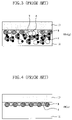
- FIGS. 1 to 4 illustrate a conventional method for forming a thin film on a substrate using atomic layer deposition.
- a first reactant of a compound, AXn(g) is supplied onto a semiconductor substrate 10 loaded in a chamber 12 , wherein A denotes a first material constituting a thin film to be deposited, and Xn denotes a material chemically combined with the material A.
- the first reactant of the AXn is bubbled and supplied in a gas state to the chamber 12 via a gas line.
- the first supplied reactant of the AXn is chemically adsorbed to the surface of the semiconductor substrate 10 .
- a purging or pumping process is conducted in the chamber to leave only the AXn(s), which has been chemically adsorbed on the semiconductor substrate. Accordingly, residues, which float in the chamber 12 or are physically adsorbed on the semiconductor substrate 10 , are drained away from the chamber 12 .
- a second reactant of a compound, BYn(g) is supplied into the chamber 12 , wherein B denotes a second material constituting the thin film to be deposited, and Yn denotes a material chemically combined with the material B.
- the second reactant of the BYn is bubbled and supplied in a gas state into the chamber 12 via a separate gas line.
- the second supplied reactant of the BYn is chemically adsorbed to the semiconductor substrate 10 , such that the thin film of AB(s) is formed by chemical displacement.
- the purging or pumping process is conducted in the chamber to leave only the thin film of the AB(s), which has been formed on the semiconductor substrate.
- the residues, which float in the chamber 12 or are physically adsorbed, are drained away from the chamber. Accordingly, a single layer of the chemically adsorbed thin film, namely, a single layer of the AB(s) is formed on the semiconductor substrate 10 .
- the processes of FIGS. 1 to 4 are repeated as one cycle a plurality of times until the thin film is formed in a desired thickness.
- the property of the formed film varies as vapor pressure of the reactant and, therefore, the reactant must be heated for sufficient supply of the reactant.
- the thin film is formed of a high dielectric material having very low vapor pressure, for example, HfO 2 , TiO 2 , Ta 2 O 5 , ZrO 2 , Nb 2 O 5 , CeO 2 , In 2 O 3 , RuO 2 or IrO 2 .
- long-time heating of the reactant makes it difficult to manage the reactant, and changes the reactant in quality. Further, it increases the supply time and removal time of the reactant, resulting in semiconductor yield reduction.
- Exemplary embodiments of the invention generally include methods and apparatus for forming thin films for semiconductor devices, which enable the supply amount of a reactant to be increased by preheating and supplying a process gas used to bubble the reactant to a certain temperature so that a heating effect of the reactant is increased, in forming the thin film on a substrate.
- Exemplary methods and apparatus for forming thin films enable enhancement of a purging effect by heating and supplying a purging gas used to remove remaining residues in a chamber at a predetermined temperature in forming the thin film on a substrate.
- Exemplary embodiments of the present invention also include methods and apparatus for forming thin films, which enable supply and removal of reactants containing constituent elements of a thin film to be formed by preheating and supplying a process gas and a purging gas at a predetermined temperature in forming the thin film on a substrate.
- a method for forming a thin film for a semiconductor device includes supplying a first reactant to a chamber to chemically adsorb the first reactant onto a substrate, the first reactant being bubbled by a first preheated and supplied gas, purging the chamber to remove residues on the substrate having the first reactant chemically adsorbed, and forming the thin film with chemical displacement by supplying a second reactant to the chamber to chemically adsorb the second reactant onto the substrate.
- the exemplary method may also include removing the residues on the substrate having the thin film by purging the chamber after forming the thin film.
- the first gas may be preheated by a heating means.
- the purging step may be performed by supplying to the chamber a purging gas preheated through the heating means.
- the second reactant supplied to the chamber may be bubbled and supplied by a second gas, the second gas being preheated through a heating means.
- the heating means may be a sheath heater, a tubular heater, a cartridge heater, a coil heater, a band heater, a jacket heater, or a ribbon heater.
- an apparatus for forming a thin film for a semiconductor device comprises a chamber into which a substrate is loaded, a first reactant supply unit for supplying a first reactant to the chamber, a first gas line for connecting between the chamber and the first reactant supply unit, a second reactant supply unit for supplying a second reactant to the chamber, a second gas line for connecting between the chamber and the second reactant supply unit, a gas supply unit for supplying a process gas to the chamber, the first reactant supply unit and the second reactant supply unit, a third gas line for connecting between the first reactant supply unit and the gas supply unit, the third gas line including a heating means for heating the process gas, a fourth gas line for connecting between the second reactant supply unit and the gas supply unit, and a fifth gas line for connecting between the chamber and the gas supply unit.
- an apparatus for forming a thin film for a semiconductor device on a substrate by means of chemical displacement by chemically adsorbing first and second bubbled reactants in sequence comprises a heating means for preheating a process gas that is supplied to bubble the first reactant.
- the apparatus may also comprise a heating means for preheating a purging gas, the purging gas being supplied to perform a purging process of removing remaining residues after the first reactant or the second reactant is chemically adsorbed.
- the apparatus may further comprise a heating means for preheating a process gas that is supplied to bubble the second reactant.
- FIGS. 1 to 4 illustrate a conventional method for forming a thin film for a semiconductor device.
- FIG. 5 schematically illustrates an apparatus for forming a thin film for a semiconductor device according to an exemplary embodiment of the present invention.
- FIG. 6 schematically illustrates an apparatus for forming a thin film for a semiconductor device according to another exemplary embodiment of the present invention.
- FIG. 7 is a graph showing step coverage of a thin film formed using thin film forming methods according to an exemplary embodiment of the present invention and according to the prior art.
- FIG. 8 a is a graph showing the thickness of a thin film formed using a thin film forming method according to the prior art.
- FIG. 8 b is a graph showing the range of a thin film formed using a thin film forming method according to the prior art.
- FIG. 9 a is a graph showing the thickness of a thin film formed using a thin film forming method according to an exemplary embodiment of the present invention.
- FIG. 9 b is a graph showing the range of a thin film formed using a thin film forming method according to an exemplary embodiment of the present invention.
- the apparatus includes a chamber 100 into which a substrate is loaded, a first reactant supply unit 110 for supplying a first reactant to the chamber, a second reactant supply unit 120 for supplying a second reactant to the chamber, a gas supply unit 130 for supplying a process gas to the chamber 100 , the first reactant supply unit 110 and the second reactant supply unit 120 , and a pump 140 for performing a pumping operation to remove remaining residues in the chamber.
- the apparatus further includes a first gas line 115 for connecting between the chamber 100 and the first reactant supply unit 110 , a second gas line 125 for connecting between the chamber 100 and the second reactant supply unit 120 , a third gas line 135 for connecting between the first reactant supply unit 110 , and the gas supply unit 130 , a fourth gas line 145 connecting between the second reactant supply unit 120 and the gas supply unit 130 , a fifth gas line 155 for connecting between the chamber 100 and the gas supply unit 130 , and a sixth gas line 165 for connecting between the chamber 100 and the pump 140 .
- the gas supply unit 130 provides to the first reactant supply unit 110 a process gas, for example, an inert gas such as an argon gas (Ar), which is heated through the third gas line 135 connected to the first reactant supply unit.
- a process gas for example, an inert gas such as an argon gas (Ar)
- the third gas line 135 may be formed in a sufficient length to effectively heat the process gas.
- the third gas line 135 may be formed in a coil shape.
- the third gas line 135 also includes a heating means capable of heating the process gas.
- the heating means may be composed of a heater, for example, a sheath heater, a tubular heater, a cartridge heater, a band heater, or a jacket heater.
- the heating means may be formed of, for example, a coil or ribbon heater having a structure in which the sheath heater, the tubular heater, or the cartridge heater is wound around the third coiled gas line 135 .
- the third gas line 135 may include a control valve 133 capable of controlling the process gas provided to the first reactant supply unit 110 .
- the gas supply unit 130 provides to the chamber 100 a process gas, namely, a purging gas that is an inert gas such as an argon gas (Ar) or a nitrogen gas (N 2 ) through the fifth gas line 155 connected to the chamber so that a purging process for removing the residues in the chamber is performed.
- the fifth gas line 155 may heat the purging gas and then provide the heated purging gas to the chamber 100 , similarly to the third gas line 135 .
- the fifth gas line 155 may be formed in a sufficient length to effectively heat the purging gas.
- the fifth gas line 155 may be formed in a coil shape.
- the fifth gas line 155 may include a heating means.
- the heating means may be, for example, a sheath heater, a tubular heater, a cartridge heater, a band heater, or a jacket heater. Further, the heater may be, for example, a coil or ribbon heater having a structure in which the sheath heater, the tubular heater, or the cartridge heater is wound around the fifth coiled gas line 155 .
- the fifth gas line 155 may include control valves 153 a and 153 b capable of controlling the purging gas, which is provided to the chamber 100 .
- the gas supply unit 130 also provides a process gas, for example, an inert gas such as an argon gas (Ar) to the second reactant supply unit 120 through the fourth gas line 145 connected to the second reactant supply unit.
- a process gas for example, an inert gas such as an argon gas (Ar)
- the fourth gas line 145 may heat the process gas and then provides the heated process gas to the second reactant supply unit 120 , similarly to the third gas line 135 .
- the fourth gas line 145 may include a control valve 143 capable of controlling the process gas provided to the second reactant supply unit 120 .
- the first reactant supply unit 110 is provided with the preheated process gas through the third gas line 135 to convert a first reactant 117 from the liquid state to a bubble state, namely, a gas state and then provide a first reaction gas to the chamber 100 through the first gas line 115 .
- the first reactant 117 varies depending on the type of the thin film, and contains a constituent element and a chemical ligand of the thin film to be formed.
- the first reaction gas for example, Tetrakis Ethyl Methyl Amino Hafnium (TEMAH), TiCl 4 , Tetrakis DiMethyl Amino Titanium (TDMAT), Tetrakis DiEthyl Amino Titanium (TDEAT), TriMethyl Aluminum (TMA), or TriEthyl Aluminum (TEA) may be provided.
- the first gas line 115 may include control valves 111 and 113 capable of controlling the first reaction gas and the purging gas provided to the chamber 100 .
- the second reactant supply unit 120 is provided with the process gas through the fourth gas line 145 .
- the second reactant supply unit 120 converts a second reactant 127 from a liquid state to a bubble state, namely, a gas state, and then provides a second reaction gas to the chamber 100 through the second gas line 125 .
- a second reaction gas H 2 O, H 2 O 2 , O 2 or O 3 as an oxidizing agent may be provided, or NH 3 , N 2 , O 2 or N 2 O as a plasma gas for removing a hydroxyl group may be provided.
- the second gas line 125 may include control valves 121 and 123 capable of controlling the second reaction gas and the purging gas provided to the chamber 100 .
- the chamber 100 includes a heater 102 for maintaining temperature in the chamber, and a shower head 106 for injecting gases into the chamber.
- the heater 102 is operable to maintain temperature of the substrate 104 loaded in the chamber at about 150 to about 375° C.
- the shower head 106 is operable to inject the gases to be supplied to the chamber into the chamber for about 0.1 to about 10 secs.
- the substrate 104 is loaded in the chamber, the substrate 104 is maintained at a predetermined temperature by the heater 102 .
- the process gas for example, the argon gas (Ar), which is heated to a predetermined temperature through the third gas line 135 including the heating means, is supplied to the first reactant supply unit to convert the first reactant 117 from a liquid state to a gas state.
- the control valves 111 and 113 which are mounted to the first gas line, are selectively operated to inject the first reaction gas into the chamber through the first gas line 115 and the shower head 106 .
- the first reaction gas supplied into the chamber is chemically adsorbed onto the substrate 104 or is physically adsorbed to the first chemically adsorbed reactant.
- the control valve 153 a or 153 b which is mounted to the fifth gas line that connects between the chamber and the gas supply unit, is operated to supply to the chamber 100 a purging gas, for example, an argon gas (Ar) or a nitrogen gas (N 2 ) heated to a predetermined temperature through the fifth gas line 155 having the heating means. Accordingly, the residues, which float in the chamber or are physically adsorbed on the substrate, are removed from the chamber. To remove the residues, a pumping process using the pump 140 may be performed in place of the purging process.
- a purging gas for example, an argon gas (Ar) or a nitrogen gas (N 2 ) heated to a predetermined temperature through the fifth gas line 155 having the heating means.
- the process gas for example, the argon gas (Ar) is supplied to the second reactant supply unit 120 through the fourth gas line 145 to convert the second reactant 127 from a liquid state to a gas state.
- the control valves 121 and 123 mounted to the second gas line are selectively operated to inject the second reaction gas into the chamber through the second gas line 125 and the shower head 106 .
- the second reaction gas supplied to the chamber is chemically adsorbed onto the substrate or is physically adsorbed onto the first and second chemically adsorbed reactants.
- the first and second chemically adsorbed reactants form a solid-state thin film on the substrate by means of chemical displacement.
- the fourth gas line includes heating means, a heated process gas may be supplied to the second reactant supply unit.
- the solid-state thin film may be formed of, for example, a single atomic thin film, a single atomic oxide, a complex oxide, a single atomic nitride film, or a complex nitride film.
- the single atomic thin film may be formed of, for example, Ti, Ta, Ru, Ir, Rh, Mo, Al, Cu, Pt, W or Ag, and the single atomic oxide may be formed of, for example; HfO 2 , TiO 2 , Ta 2 O 5 , ZrO 2 , Nb 2 O 5 , CeO 2 , In 2 O 3 , RuO 2 , IrO 2 or Al 2 O 3 .
- the complex oxide may be formed of SrTiO 3 , PbTiO 3 , SrRuO 3 , CaRuO 3 , (Ba, Sr)TiO 3 , Pb(Zr,Ti)O 3 , (Pb, La)(Zr,Ti)O 3 , (Sr,Ca)RuO 3 , In 2 O 3 doped with Sn, In 2 O 3 doped with Fe, or In 2 O 3 doped with Zr.
- the single atomic nitride film may be formed of TiN, TaN, NbN, ZrN, Ya 3 N 5 , SiN, AlN, GaN, WN or BN.
- the complex nitride film may be formed of TiSiN, TaSiN, AlTiN, WBN, WSiN or AlSiN.
- control valve 153 a or 153 b which is mounted to the fifth gas line that connects the chamber and the gas supply unit, is operated to supply to the chamber 100 the purging gas, for example, the argon gas (Ar) or the nitrogen gas (N 2 ) heated to a predetermined temperature through the fifth gas line 155 having the heating means. Accordingly, the residues, which float in the chamber or are physically adsorbed on the substrate, are removed from the chamber. As a result, a single layer of the chemically adsorbed thin film is formed on the substrate. A pumping process using the pump 140 may be performed in place of the purging process to remove the residues.
- the purging gas for example, the argon gas (Ar) or the nitrogen gas (N 2 ) heated to a predetermined temperature through the fifth gas line 155 having the heating means.
- FIG. 6 schematically illustrates an apparatus for forming a thin film for a semiconductor device in accordance with another exemplary embodiment of the present invention.
- the identical or similar portions to those of the thin film forming apparatus of FIG. 5 will be roughly described and it should not be construed as limiting the scope of the present invention.
- the apparatus for forming a thin film in accordance with another exemplary embodiment of the present invention includes a chamber 100 into which a substrate is loaded, a first reactant supply unit 110 for supplying a first reactant to the chamber, a second reactant supply unit 120 for supplying a second reactant to the chamber, a gas supply unit 130 for supplying a process gas to the chamber 100 , the first reactant supply unit 110 and the second reactant supply unit 120 , and a pump 140 for performing a pumping operation to remove remaining residues in the chamber.
- the apparatus further includes a first gas line 115 for connecting between the chamber 100 and the first reactant supply unit 110 , a second gas line 125 for connecting between the chamber 100 and the second reactant supply unit 120 , a third gas line 135 for connecting between the first reactant supply unit 110 and the gas supply unit 130 , a fourth gas line 146 connecting between the second reactant supply unit 120 and the gas supply unit 130 , a fifth gas line 155 for connecting between the chamber 100 and the gas supply unit 130 , and a sixth gas line 165 for connecting between the chamber 100 and the pump 140 .
- the gas supply unit 130 provides to the first reactant supply unit 110 a process gas, for example, an inert gas such as an argon gas (Ar), which is heated through the third gas line 135 connected to the first reactant supply unit.
- the gas supply unit 130 also provides to the chamber 100 a process gas, namely, a purging gas such as the argon gas (Ar) or a nitrogen gas (N 2 ) through the fifth gas line 155 connected to the chamber so that a purging process for removing the residues in the chamber is performed.
- the gas supply unit 130 also provides a process gas to the second reactant supply unit 120 .
- the process gas is an inert gas, e.g., an argon gas (Ar).
- the process gas may be heated through the fourth gas line 146 connected to the second reactant supply unit.
- the third, fourth and fifth gas lines 135 , 146 and 155 may be formed in a sufficient length to effectively heat the process gas or the purging gas.
- the third, fourth and fifth gas lines 135 , 146 and 155 may be formed in a coil shape.
- the third, fourth and fifth gas lines 135 , 146 and 155 include a heating means capable of heating the process gas or the purging gas.
- the heating means may be, for example, a sheath heater, a tubular heater, a cartridge heater, a band heater, or a jacket heater.
- the heating means may be, for example, a coil or ribbon heater having a structure in which the sheath heater, the tubular heater, or the cartridge heater is wound around the third, fourth and fifth coiled gas lines 135 , 146 and 155 .
- the third, fourth and fifth gas lines 135 , 146 and 155 may include control valves 133 , 143 , and 153 a and 153 b capable of controlling the process gas or the purging gas, respectively.
- the first reactant supply unit 110 is provided with the preheated process gas through the third gas line 135 to convert a first reactant from a liquid state to a bubble state, namely, a gas state and then to provide a first reaction gas to the chamber 100 through the first gas line 115 .
- the second reactant supply unit 120 is provided with the process gas through the fourth gas line 145 to convert a second reactant from a liquid state to a bubble state, namely, a gas state and then to provide a second reaction gas to the chamber 100 through the second gas line 125 .
- the first gas line 115 may include control valves 111 and 113 and the second gas line 125 may include control valves 121 and 123 capable of controlling the reaction gas or the purging gas, which is provided to the chamber 100 .
- the chamber 100 includes a heater 102 for maintaining temperature in the chamber, and a shower head 106 for injecting gases into the chamber.
- the heater 102 is operable to maintain temperature of the substrate 104 loaded in the chamber at about 150 to about 375° C.
- the shower head 106 is operable to inject the gases to be supplied to the chamber into the chamber for about 0.1 to about 10 secs.
- FIG. 7 is a graph showing step coverage of a thin film formed using a thin film forming method in accordance with the present invention. It shows a result of an experiment in which a hafnium oxide (HfO 2 ) film is formed on a substrate, wherein the TEMAH, which is a liquid compound having the highest volatility among hafnium amide system compounds, is used as a source gas and an argon gas (Ar), heated to about 80° C., is used as a process gas.
- An abscissa axis of the graph indicates the position of a wafer and an ordinate axis indicates step coverage in a bottom portion at a relevant wafer position.
- TT indicates a top portion of the wafer
- C indicates a center of the wafer
- LL indicates a side (leftmost side) of the wafer.
- T indicates an intermediate point between the top portion and the center of the wafer
- CBL indicates a 45° point moving from an intermediate point between the side and the center of the wafer to the bottom side.
- bottom portion step coverage at the TT point is about 60 when a non-heated process gas is supplied to form the thin film in accordance with a prior art while the step coverage at the same point is improved and is about 150 when the process gas is heated to a predetermined temperature and is supplied to form the thin film in accordance with an exemplary embodiment of the present invention.
- the T, C, LL, and CBL points have step coverage of 178, 180, 60 and 140, respectively, while in an exemplary embodiment of the present invention, the TT, T, C, LL, and CBL points have step coverage of about 150, about 200, about 200, about 110, and about 180, respectively. It shows that the step coverage is significantly improved compared to the prior art, as well as deviation of the step coverage is significantly reduced.
- FIG. 8 a is a graph showing the thickness of a thin film formed using the thin film forming method in accordance with the prior art
- FIG. 9 a is a graph showing the thickness of a thin film formed using the thin film forming method in accordance with an exemplary embodiment of the present invention.
- the thickness of the thin film formed using the thin film forming method in accordance with an exemplary embodiment of the present invention has much higher uniformity than that of the thin film formed using the thin film forming method in accordance with the prior art.
- FIG. 8 b is a graph showing the range of a thin film formed using a thin film forming method in accordance with a prior art
- FIG. 9 b is a graph showing the range of a thin film formed using a thin film forming method in accordance with an exemplary embodiment of the present invention.
- the thin film formed using the thin film forming method in accordance with an exemplary embodiment of the present invention has a much narrower range than that of the thin film formed using the thin film forming method in accordance with the prior art.
- the thin film forming method in accordance with an exemplary embodiment of the present invention it is possible to increase the supply amount of the reactant by preheating and supplying the process gas used to bubble the reactant to a certain temperature so that the heating effect of the reactant is enhanced.
- the present invention has an advantage that the supply amount of the reactant can be increased by preheating and supplying the process gas used to bubble the reactant to a certain temperature so that a heating effect of the reactant is enhanced, in forming the thin film on the substrate.
- the present invention has an advantage that the purging effect is enhanced by heating and supplying the purging gas used to remove remaining residues in the chamber to a certain temperature in forming the thin film on the substrate.
- the present invention has an advantage that reactants containing constituent elements of a thin film to be formed can be smoothly supplied and removed by preheating and supplying the process gas and the purging gas to a certain temperature in forming the thin film on the substrate.
Abstract
Description
Claims (27)
Priority Applications (1)
| Application Number | Priority Date | Filing Date | Title |
|---|---|---|---|
| US11/838,998 US20080029031A1 (en) | 2004-01-20 | 2007-08-15 | Methods and apparatus for forming thin films for semiconductor devices |
Applications Claiming Priority (2)
| Application Number | Priority Date | Filing Date | Title |
|---|---|---|---|
| KR2004-4212 | 2004-01-20 | ||
| KR1020040004212A KR100621765B1 (en) | 2004-01-20 | 2004-01-20 | Method for forming thin film in semiconductor device and apparatus thereof |
Related Child Applications (1)
| Application Number | Title | Priority Date | Filing Date |
|---|---|---|---|
| US11/838,998 Division US20080029031A1 (en) | 2004-01-20 | 2007-08-15 | Methods and apparatus for forming thin films for semiconductor devices |
Publications (2)
| Publication Number | Publication Date |
|---|---|
| US20050158977A1 US20050158977A1 (en) | 2005-07-21 |
| US7273822B2 true US7273822B2 (en) | 2007-09-25 |
Family
ID=34747900
Family Applications (2)
| Application Number | Title | Priority Date | Filing Date |
|---|---|---|---|
| US11/038,324 Active 2025-05-17 US7273822B2 (en) | 2004-01-20 | 2005-01-19 | Methods and apparatus for forming thin films for semiconductor devices |
| US11/838,998 Abandoned US20080029031A1 (en) | 2004-01-20 | 2007-08-15 | Methods and apparatus for forming thin films for semiconductor devices |
Family Applications After (1)
| Application Number | Title | Priority Date | Filing Date |
|---|---|---|---|
| US11/838,998 Abandoned US20080029031A1 (en) | 2004-01-20 | 2007-08-15 | Methods and apparatus for forming thin films for semiconductor devices |
Country Status (2)
| Country | Link |
|---|---|
| US (2) | US7273822B2 (en) |
| KR (1) | KR100621765B1 (en) |
Cited By (5)
| Publication number | Priority date | Publication date | Assignee | Title |
|---|---|---|---|---|
| US8791034B2 (en) | 2009-06-26 | 2014-07-29 | Cornell University | Chemical vapor deposition process for aluminum silicon nitride |
| US9306050B2 (en) | 2009-06-26 | 2016-04-05 | Cornell University | III-V semiconductor structures including aluminum-silicon nitride passivation |
| US20180096886A1 (en) * | 2016-09-30 | 2018-04-05 | Lam Research Corporation | Composite dielectric interface layers for interconnect structures |
| US10651080B2 (en) | 2016-04-26 | 2020-05-12 | Lam Research Corporation | Oxidizing treatment of aluminum nitride films in semiconductor device manufacturing |
| US10665501B2 (en) | 2016-11-14 | 2020-05-26 | Lam Research Corporation | Deposition of Aluminum oxide etch stop layers |
Families Citing this family (4)
| Publication number | Priority date | Publication date | Assignee | Title |
|---|---|---|---|---|
| US7192849B2 (en) * | 2003-05-07 | 2007-03-20 | Sensor Electronic Technology, Inc. | Methods of growing nitride-based film using varying pulses |
| KR100829608B1 (en) * | 2006-08-30 | 2008-05-14 | 삼성전자주식회사 | Method of manufacturing a thin layer and methods of manufacturing a gate structure and a capacitor using the same |
| US8741062B2 (en) * | 2008-04-22 | 2014-06-03 | Picosun Oy | Apparatus and methods for deposition reactors |
| JP6107690B2 (en) * | 2013-09-27 | 2017-04-05 | 東京エレクトロン株式会社 | Pretreatment method for filter unit, treatment liquid supply device, filter unit heating device |
Citations (5)
| Publication number | Priority date | Publication date | Assignee | Title |
|---|---|---|---|---|
| US6391785B1 (en) | 1999-08-24 | 2002-05-21 | Interuniversitair Microelektronica Centrum (Imec) | Method for bottomless deposition of barrier layers in integrated circuit metallization schemes |
| US20030003635A1 (en) | 2001-05-23 | 2003-01-02 | Paranjpe Ajit P. | Atomic layer deposition for fabricating thin films |
| US6620670B2 (en) | 2002-01-18 | 2003-09-16 | Applied Materials, Inc. | Process conditions and precursors for atomic layer deposition (ALD) of AL2O3 |
| US20050012975A1 (en) * | 2002-12-17 | 2005-01-20 | George Steven M. | Al2O3 atomic layer deposition to enhance the deposition of hydrophobic or hydrophilic coatings on micro-electromechcanical devices |
| US7007933B2 (en) * | 2002-08-30 | 2006-03-07 | Samsung Electronics Co., Ltd. | Method and apparatus for supplying a source gas |
Family Cites Families (1)
| Publication number | Priority date | Publication date | Assignee | Title |
|---|---|---|---|---|
| US6106898A (en) * | 1997-11-28 | 2000-08-22 | Japan Pionics, Co., Ltd. | Process for preparing nitride film |
-
2004
- 2004-01-20 KR KR1020040004212A patent/KR100621765B1/en active IP Right Grant
-
2005
- 2005-01-19 US US11/038,324 patent/US7273822B2/en active Active
-
2007
- 2007-08-15 US US11/838,998 patent/US20080029031A1/en not_active Abandoned
Patent Citations (5)
| Publication number | Priority date | Publication date | Assignee | Title |
|---|---|---|---|---|
| US6391785B1 (en) | 1999-08-24 | 2002-05-21 | Interuniversitair Microelektronica Centrum (Imec) | Method for bottomless deposition of barrier layers in integrated circuit metallization schemes |
| US20030003635A1 (en) | 2001-05-23 | 2003-01-02 | Paranjpe Ajit P. | Atomic layer deposition for fabricating thin films |
| US6620670B2 (en) | 2002-01-18 | 2003-09-16 | Applied Materials, Inc. | Process conditions and precursors for atomic layer deposition (ALD) of AL2O3 |
| US7007933B2 (en) * | 2002-08-30 | 2006-03-07 | Samsung Electronics Co., Ltd. | Method and apparatus for supplying a source gas |
| US20050012975A1 (en) * | 2002-12-17 | 2005-01-20 | George Steven M. | Al2O3 atomic layer deposition to enhance the deposition of hydrophobic or hydrophilic coatings on micro-electromechcanical devices |
Cited By (9)
| Publication number | Priority date | Publication date | Assignee | Title |
|---|---|---|---|---|
| US8791034B2 (en) | 2009-06-26 | 2014-07-29 | Cornell University | Chemical vapor deposition process for aluminum silicon nitride |
| US9306050B2 (en) | 2009-06-26 | 2016-04-05 | Cornell University | III-V semiconductor structures including aluminum-silicon nitride passivation |
| US9991360B2 (en) | 2009-06-26 | 2018-06-05 | Cornell University | Method for forming III-V semiconductor structures including aluminum-silicon nitride passivation |
| US10651080B2 (en) | 2016-04-26 | 2020-05-12 | Lam Research Corporation | Oxidizing treatment of aluminum nitride films in semiconductor device manufacturing |
| US20180096886A1 (en) * | 2016-09-30 | 2018-04-05 | Lam Research Corporation | Composite dielectric interface layers for interconnect structures |
| US10049869B2 (en) * | 2016-09-30 | 2018-08-14 | Lam Research Corporation | Composite dielectric interface layers for interconnect structures |
| US10418236B2 (en) * | 2016-09-30 | 2019-09-17 | Lam Research Corporation | Composite dielectric interface layers for interconnect structures |
| US10665501B2 (en) | 2016-11-14 | 2020-05-26 | Lam Research Corporation | Deposition of Aluminum oxide etch stop layers |
| US10804144B2 (en) | 2016-11-14 | 2020-10-13 | Lam Research Corporation | Deposition of aluminum oxide etch stop layers |
Also Published As
| Publication number | Publication date |
|---|---|
| US20050158977A1 (en) | 2005-07-21 |
| KR100621765B1 (en) | 2006-09-08 |
| KR20050076287A (en) | 2005-07-26 |
| US20080029031A1 (en) | 2008-02-07 |
Similar Documents
| Publication | Publication Date | Title |
|---|---|---|
| US7273822B2 (en) | Methods and apparatus for forming thin films for semiconductor devices | |
| KR101379015B1 (en) | METHOD OF DEPOSITING Ru FILM USING PEALD AND DENSE Ru FILM | |
| JP4057184B2 (en) | Thin film manufacturing method using atomic layer deposition | |
| JP4167411B2 (en) | Thin film formation method using atomic layer deposition | |
| US6720259B2 (en) | Passivation method for improved uniformity and repeatability for atomic layer deposition and chemical vapor deposition | |
| US8808455B2 (en) | Substrate processing apparatus and method of manufacturing semiconductor device | |
| KR100385947B1 (en) | Method of forming thin film by atomic layer deposition | |
| US7247581B2 (en) | Methods for treating pluralities of discrete semiconductor substrates | |
| US8049304B2 (en) | Constructions comprising hafnium oxide and/or zirconium oxide | |
| JP3670628B2 (en) | Film forming method, film forming apparatus, and semiconductor device manufacturing method | |
| US7094690B1 (en) | Deposition methods and apparatuses providing surface activation | |
| KR100652420B1 (en) | Method of manufacturing a dielectric film and method of manufacturing Metal Insulator Metal capacitor having the dielectric film and batch type atomic layer deposition apparatus for manufacturing the dielectric film | |
| US20060045970A1 (en) | ALD thin film deposition apparatus and thin film deposition method using same | |
| JP2000160342A (en) | Production of thin film | |
| US20060128127A1 (en) | Method of depositing a metal compound layer and apparatus for depositing a metal compound layer | |
| KR20010065160A (en) | Method of forming a aluminum oxide thin film in a semiconductor device | |
| US8039054B2 (en) | Layer deposition methods | |
| TWI389184B (en) | Film forming method, film forming apparatus and memory medium | |
| KR100319880B1 (en) | Method for manufacturing thin film using atomic layer deposition | |
| KR100511914B1 (en) | Method for fabricating of semiconductor device using PECYCLE-CVD | |
| KR20210148279A (en) | A film forming method, a semiconductor device manufacturing method, a film forming apparatus, and a system for manufacturing a semiconductor device | |
| KR20070038262A (en) | Apparatus for depositing an atomic layer |
Legal Events
| Date | Code | Title | Description |
|---|---|---|---|
| AS | Assignment |
Owner name: SAMSUNG ELECTRONICS CO., LTD., KOREA, REPUBLIC OF Free format text: ASSIGNMENT OF ASSIGNORS INTEREST;ASSIGNORS:YEO, JAE-HYUN;PARK, YOUNG-WOOK;KIM, KI-CHUL;AND OTHERS;REEL/FRAME:016201/0890;SIGNING DATES FROM 20050117 TO 20050118 |
|
| STCF | Information on status: patent grant |
Free format text: PATENTED CASE |
|
| FEPP | Fee payment procedure |
Free format text: PAYOR NUMBER ASSIGNED (ORIGINAL EVENT CODE: ASPN); ENTITY STATUS OF PATENT OWNER: LARGE ENTITY |
|
| FPAY | Fee payment |
Year of fee payment: 4 |
|
| FPAY | Fee payment |
Year of fee payment: 8 |
|
| MAFP | Maintenance fee payment |
Free format text: PAYMENT OF MAINTENANCE FEE, 12TH YEAR, LARGE ENTITY (ORIGINAL EVENT CODE: M1553); ENTITY STATUS OF PATENT OWNER: LARGE ENTITY Year of fee payment: 12 |