US7170101B2 - Nitride-based semiconductor light-emitting device and manufacturing method thereof - Google Patents
Nitride-based semiconductor light-emitting device and manufacturing method thereof Download PDFInfo
- Publication number
- US7170101B2 US7170101B2 US10/146,412 US14641202A US7170101B2 US 7170101 B2 US7170101 B2 US 7170101B2 US 14641202 A US14641202 A US 14641202A US 7170101 B2 US7170101 B2 US 7170101B2
- Authority
- US
- United States
- Prior art keywords
- metal
- nitride
- gan substrate
- semiconductor light
- emitting device
- Prior art date
- Legal status (The legal status is an assumption and is not a legal conclusion. Google has not performed a legal analysis and makes no representation as to the accuracy of the status listed.)
- Expired - Fee Related, expires
Links
Images


Classifications
-
- H—ELECTRICITY
- H01—ELECTRIC ELEMENTS
- H01L—SEMICONDUCTOR DEVICES NOT COVERED BY CLASS H10
- H01L33/00—Semiconductor devices with at least one potential-jump barrier or surface barrier specially adapted for light emission; Processes or apparatus specially adapted for the manufacture or treatment thereof or of parts thereof; Details thereof
- H01L33/02—Semiconductor devices with at least one potential-jump barrier or surface barrier specially adapted for light emission; Processes or apparatus specially adapted for the manufacture or treatment thereof or of parts thereof; Details thereof characterised by the semiconductor bodies
- H01L33/26—Materials of the light emitting region
- H01L33/30—Materials of the light emitting region containing only elements of group III and group V of the periodic system
- H01L33/32—Materials of the light emitting region containing only elements of group III and group V of the periodic system containing nitrogen
-
- H—ELECTRICITY
- H01—ELECTRIC ELEMENTS
- H01L—SEMICONDUCTOR DEVICES NOT COVERED BY CLASS H10
- H01L24/00—Arrangements for connecting or disconnecting semiconductor or solid-state bodies; Methods or apparatus related thereto
- H01L24/01—Means for bonding being attached to, or being formed on, the surface to be connected, e.g. chip-to-package, die-attach, "first-level" interconnects; Manufacturing methods related thereto
- H01L24/26—Layer connectors, e.g. plate connectors, solder or adhesive layers; Manufacturing methods related thereto
- H01L24/31—Structure, shape, material or disposition of the layer connectors after the connecting process
- H01L24/32—Structure, shape, material or disposition of the layer connectors after the connecting process of an individual layer connector
-
- H—ELECTRICITY
- H01—ELECTRIC ELEMENTS
- H01S—DEVICES USING THE PROCESS OF LIGHT AMPLIFICATION BY STIMULATED EMISSION OF RADIATION [LASER] TO AMPLIFY OR GENERATE LIGHT; DEVICES USING STIMULATED EMISSION OF ELECTROMAGNETIC RADIATION IN WAVE RANGES OTHER THAN OPTICAL
- H01S5/00—Semiconductor lasers
- H01S5/02—Structural details or components not essential to laser action
- H01S5/022—Mountings; Housings
- H01S5/023—Mount members, e.g. sub-mount members
- H01S5/0231—Stems
-
- H—ELECTRICITY
- H01—ELECTRIC ELEMENTS
- H01S—DEVICES USING THE PROCESS OF LIGHT AMPLIFICATION BY STIMULATED EMISSION OF RADIATION [LASER] TO AMPLIFY OR GENERATE LIGHT; DEVICES USING STIMULATED EMISSION OF ELECTROMAGNETIC RADIATION IN WAVE RANGES OTHER THAN OPTICAL
- H01S5/00—Semiconductor lasers
- H01S5/04—Processes or apparatus for excitation, e.g. pumping, e.g. by electron beams
- H01S5/042—Electrical excitation ; Circuits therefor
- H01S5/0425—Electrodes, e.g. characterised by the structure
- H01S5/04252—Electrodes, e.g. characterised by the structure characterised by the material
-
- H—ELECTRICITY
- H01—ELECTRIC ELEMENTS
- H01S—DEVICES USING THE PROCESS OF LIGHT AMPLIFICATION BY STIMULATED EMISSION OF RADIATION [LASER] TO AMPLIFY OR GENERATE LIGHT; DEVICES USING STIMULATED EMISSION OF ELECTROMAGNETIC RADIATION IN WAVE RANGES OTHER THAN OPTICAL
- H01S5/00—Semiconductor lasers
- H01S5/30—Structure or shape of the active region; Materials used for the active region
- H01S5/32—Structure or shape of the active region; Materials used for the active region comprising PN junctions, e.g. hetero- or double- heterostructures
- H01S5/323—Structure or shape of the active region; Materials used for the active region comprising PN junctions, e.g. hetero- or double- heterostructures in AIIIBV compounds, e.g. AlGaAs-laser, InP-based laser
- H01S5/32308—Structure or shape of the active region; Materials used for the active region comprising PN junctions, e.g. hetero- or double- heterostructures in AIIIBV compounds, e.g. AlGaAs-laser, InP-based laser emitting light at a wavelength less than 900 nm
- H01S5/32341—Structure or shape of the active region; Materials used for the active region comprising PN junctions, e.g. hetero- or double- heterostructures in AIIIBV compounds, e.g. AlGaAs-laser, InP-based laser emitting light at a wavelength less than 900 nm blue laser based on GaN or GaP
-
- H—ELECTRICITY
- H01—ELECTRIC ELEMENTS
- H01L—SEMICONDUCTOR DEVICES NOT COVERED BY CLASS H10
- H01L2224/00—Indexing scheme for arrangements for connecting or disconnecting semiconductor or solid-state bodies and methods related thereto as covered by H01L24/00
- H01L2224/01—Means for bonding being attached to, or being formed on, the surface to be connected, e.g. chip-to-package, die-attach, "first-level" interconnects; Manufacturing methods related thereto
- H01L2224/26—Layer connectors, e.g. plate connectors, solder or adhesive layers; Manufacturing methods related thereto
- H01L2224/31—Structure, shape, material or disposition of the layer connectors after the connecting process
- H01L2224/32—Structure, shape, material or disposition of the layer connectors after the connecting process of an individual layer connector
- H01L2224/321—Disposition
- H01L2224/32151—Disposition the layer connector connecting between a semiconductor or solid-state body and an item not being a semiconductor or solid-state body, e.g. chip-to-substrate, chip-to-passive
- H01L2224/32221—Disposition the layer connector connecting between a semiconductor or solid-state body and an item not being a semiconductor or solid-state body, e.g. chip-to-substrate, chip-to-passive the body and the item being stacked
- H01L2224/32245—Disposition the layer connector connecting between a semiconductor or solid-state body and an item not being a semiconductor or solid-state body, e.g. chip-to-substrate, chip-to-passive the body and the item being stacked the item being metallic
- H01L2224/32257—Disposition the layer connector connecting between a semiconductor or solid-state body and an item not being a semiconductor or solid-state body, e.g. chip-to-substrate, chip-to-passive the body and the item being stacked the item being metallic the layer connector connecting to a bonding area disposed in a recess of the surface of the item
-
- H—ELECTRICITY
- H01—ELECTRIC ELEMENTS
- H01L—SEMICONDUCTOR DEVICES NOT COVERED BY CLASS H10
- H01L2224/00—Indexing scheme for arrangements for connecting or disconnecting semiconductor or solid-state bodies and methods related thereto as covered by H01L24/00
- H01L2224/01—Means for bonding being attached to, or being formed on, the surface to be connected, e.g. chip-to-package, die-attach, "first-level" interconnects; Manufacturing methods related thereto
- H01L2224/42—Wire connectors; Manufacturing methods related thereto
- H01L2224/47—Structure, shape, material or disposition of the wire connectors after the connecting process
- H01L2224/48—Structure, shape, material or disposition of the wire connectors after the connecting process of an individual wire connector
- H01L2224/4805—Shape
- H01L2224/4809—Loop shape
- H01L2224/48091—Arched
-
- H—ELECTRICITY
- H01—ELECTRIC ELEMENTS
- H01L—SEMICONDUCTOR DEVICES NOT COVERED BY CLASS H10
- H01L2224/00—Indexing scheme for arrangements for connecting or disconnecting semiconductor or solid-state bodies and methods related thereto as covered by H01L24/00
- H01L2224/01—Means for bonding being attached to, or being formed on, the surface to be connected, e.g. chip-to-package, die-attach, "first-level" interconnects; Manufacturing methods related thereto
- H01L2224/42—Wire connectors; Manufacturing methods related thereto
- H01L2224/47—Structure, shape, material or disposition of the wire connectors after the connecting process
- H01L2224/48—Structure, shape, material or disposition of the wire connectors after the connecting process of an individual wire connector
- H01L2224/481—Disposition
- H01L2224/48151—Connecting between a semiconductor or solid-state body and an item not being a semiconductor or solid-state body, e.g. chip-to-substrate, chip-to-passive
- H01L2224/48221—Connecting between a semiconductor or solid-state body and an item not being a semiconductor or solid-state body, e.g. chip-to-substrate, chip-to-passive the body and the item being stacked
- H01L2224/48245—Connecting between a semiconductor or solid-state body and an item not being a semiconductor or solid-state body, e.g. chip-to-substrate, chip-to-passive the body and the item being stacked the item being metallic
- H01L2224/48247—Connecting between a semiconductor or solid-state body and an item not being a semiconductor or solid-state body, e.g. chip-to-substrate, chip-to-passive the body and the item being stacked the item being metallic connecting the wire to a bond pad of the item
-
- H—ELECTRICITY
- H01—ELECTRIC ELEMENTS
- H01L—SEMICONDUCTOR DEVICES NOT COVERED BY CLASS H10
- H01L2924/00—Indexing scheme for arrangements or methods for connecting or disconnecting semiconductor or solid-state bodies as covered by H01L24/00
- H01L2924/10—Details of semiconductor or other solid state devices to be connected
- H01L2924/11—Device type
- H01L2924/12—Passive devices, e.g. 2 terminal devices
- H01L2924/1204—Optical Diode
- H01L2924/12041—LED
-
- H—ELECTRICITY
- H01—ELECTRIC ELEMENTS
- H01L—SEMICONDUCTOR DEVICES NOT COVERED BY CLASS H10
- H01L2924/00—Indexing scheme for arrangements or methods for connecting or disconnecting semiconductor or solid-state bodies as covered by H01L24/00
- H01L2924/10—Details of semiconductor or other solid state devices to be connected
- H01L2924/11—Device type
- H01L2924/12—Passive devices, e.g. 2 terminal devices
- H01L2924/1204—Optical Diode
- H01L2924/12042—LASER
-
- H—ELECTRICITY
- H01—ELECTRIC ELEMENTS
- H01L—SEMICONDUCTOR DEVICES NOT COVERED BY CLASS H10
- H01L2924/00—Indexing scheme for arrangements or methods for connecting or disconnecting semiconductor or solid-state bodies as covered by H01L24/00
- H01L2924/15—Details of package parts other than the semiconductor or other solid state devices to be connected
- H01L2924/181—Encapsulation
-
- H—ELECTRICITY
- H01—ELECTRIC ELEMENTS
- H01L—SEMICONDUCTOR DEVICES NOT COVERED BY CLASS H10
- H01L2924/00—Indexing scheme for arrangements or methods for connecting or disconnecting semiconductor or solid-state bodies as covered by H01L24/00
- H01L2924/30—Technical effects
- H01L2924/35—Mechanical effects
- H01L2924/351—Thermal stress
-
- H—ELECTRICITY
- H01—ELECTRIC ELEMENTS
- H01S—DEVICES USING THE PROCESS OF LIGHT AMPLIFICATION BY STIMULATED EMISSION OF RADIATION [LASER] TO AMPLIFY OR GENERATE LIGHT; DEVICES USING STIMULATED EMISSION OF ELECTROMAGNETIC RADIATION IN WAVE RANGES OTHER THAN OPTICAL
- H01S5/00—Semiconductor lasers
- H01S5/02—Structural details or components not essential to laser action
- H01S5/0201—Separation of the wafer into individual elements, e.g. by dicing, cleaving, etching or directly during growth
- H01S5/0202—Cleaving
-
- H—ELECTRICITY
- H01—ELECTRIC ELEMENTS
- H01S—DEVICES USING THE PROCESS OF LIGHT AMPLIFICATION BY STIMULATED EMISSION OF RADIATION [LASER] TO AMPLIFY OR GENERATE LIGHT; DEVICES USING STIMULATED EMISSION OF ELECTROMAGNETIC RADIATION IN WAVE RANGES OTHER THAN OPTICAL
- H01S5/00—Semiconductor lasers
- H01S5/02—Structural details or components not essential to laser action
- H01S5/022—Mountings; Housings
- H01S5/02218—Material of the housings; Filling of the housings
- H01S5/02234—Resin-filled housings; the housings being made of resin
-
- H—ELECTRICITY
- H01—ELECTRIC ELEMENTS
- H01S—DEVICES USING THE PROCESS OF LIGHT AMPLIFICATION BY STIMULATED EMISSION OF RADIATION [LASER] TO AMPLIFY OR GENERATE LIGHT; DEVICES USING STIMULATED EMISSION OF ELECTROMAGNETIC RADIATION IN WAVE RANGES OTHER THAN OPTICAL
- H01S5/00—Semiconductor lasers
- H01S5/02—Structural details or components not essential to laser action
- H01S5/022—Mountings; Housings
- H01S5/0233—Mounting configuration of laser chips
- H01S5/02345—Wire-bonding
-
- H—ELECTRICITY
- H01—ELECTRIC ELEMENTS
- H01S—DEVICES USING THE PROCESS OF LIGHT AMPLIFICATION BY STIMULATED EMISSION OF RADIATION [LASER] TO AMPLIFY OR GENERATE LIGHT; DEVICES USING STIMULATED EMISSION OF ELECTROMAGNETIC RADIATION IN WAVE RANGES OTHER THAN OPTICAL
- H01S5/00—Semiconductor lasers
- H01S5/20—Structure or shape of the semiconductor body to guide the optical wave ; Confining structures perpendicular to the optical axis, e.g. index or gain guiding, stripe geometry, broad area lasers, gain tailoring, transverse or lateral reflectors, special cladding structures, MQW barrier reflection layers
- H01S5/22—Structure or shape of the semiconductor body to guide the optical wave ; Confining structures perpendicular to the optical axis, e.g. index or gain guiding, stripe geometry, broad area lasers, gain tailoring, transverse or lateral reflectors, special cladding structures, MQW barrier reflection layers having a ridge or stripe structure
- H01S5/2201—Structure or shape of the semiconductor body to guide the optical wave ; Confining structures perpendicular to the optical axis, e.g. index or gain guiding, stripe geometry, broad area lasers, gain tailoring, transverse or lateral reflectors, special cladding structures, MQW barrier reflection layers having a ridge or stripe structure in a specific crystallographic orientation
-
- H—ELECTRICITY
- H01—ELECTRIC ELEMENTS
- H01S—DEVICES USING THE PROCESS OF LIGHT AMPLIFICATION BY STIMULATED EMISSION OF RADIATION [LASER] TO AMPLIFY OR GENERATE LIGHT; DEVICES USING STIMULATED EMISSION OF ELECTROMAGNETIC RADIATION IN WAVE RANGES OTHER THAN OPTICAL
- H01S5/00—Semiconductor lasers
- H01S5/20—Structure or shape of the semiconductor body to guide the optical wave ; Confining structures perpendicular to the optical axis, e.g. index or gain guiding, stripe geometry, broad area lasers, gain tailoring, transverse or lateral reflectors, special cladding structures, MQW barrier reflection layers
- H01S5/22—Structure or shape of the semiconductor body to guide the optical wave ; Confining structures perpendicular to the optical axis, e.g. index or gain guiding, stripe geometry, broad area lasers, gain tailoring, transverse or lateral reflectors, special cladding structures, MQW barrier reflection layers having a ridge or stripe structure
- H01S5/223—Buried stripe structure
- H01S5/2231—Buried stripe structure with inner confining structure only between the active layer and the upper electrode
Definitions
- the present invention relates to nitride-based semiconductor light-emitting devices.
- Nitride-based semiconductor is used as a material for high-brightness blue LED (light-emitting diode) and pure green LED that have already been employed for full-color displays for example.
- nitride-based semiconductor is being developed for use in a semiconductor laser as a short-wavelength light source, for the purpose of increasing the storage capacity of an optical disk.
- These devices have been formed on an insulating sapphire substrate, and thus it is impossible to direct electric current from the rear side of the substrate. Accordingly, p-type and n-type electrodes are formed on the front side, which requires a complicated process for fabricating the electrodes.
- a mask member is partially formed on a sapphire substrate for growth thereon (selective lateral growth), and then a high-quality n-GaN bulk crystal is produced by hydride vapor phase growth.
- the bulk crystal is used as a substrate having its rear side from which electric current can be directed.
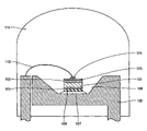
- FIG. 6 shows a cross section of a semiconductor light-emitting device including, as a light-emitting element, an LED chip formed of nitride-based compound semiconductor.
- the LED chip includes an n-GaN substrate 601 with (0001) or c-plane on which a nitride-based compound semiconductor multilayer film 602 is formed.
- Nitride-based compound semiconductor multilayer film 602 includes a buffer layer, an n-GaN cladding layer, a multiple quantum well active layer, a p-AlGaN protective layer, and a p-GaN contact layer that are successively deposited.
- a p-type translucent electrode 603 and a P pad electrode 604 are formed on the uppermost surface of nitride-based compound semiconductor multilayer film 602 .
- an n-type electrode 605 formed of stacked Ti and Al is formed on the rear surface of n-GaN substrate 601 .
- the LED chip is 350 ⁇ m ⁇ 350 ⁇ m in size.
- the LED chip is attached firmly onto a cup 608 of a leadframe 607 with Ag paste 606 , and the LED chip and leadframe 607 are electrically connected by P pad electrode 604 and a wire 609 and by n-type electrode 605 and Ag paste 606 .
- Leadframe 607 with the LED chip mounted thereon and wire 609 are encapsulated in mold resin 610 to form a semiconductor light-emitting device.
- the semiconductor light-emitting device has characteristics that the luminance is 3.0 Cd and the operating voltage is 3.5 V at room temperature under a current of 20 mA. It is noted that the luminance and operating voltage are hereinafter represented as values measured at room temperature under a current of 20 mA.
- 100 semiconductor light-emitting devices as described above are prepared on which an energization test is conducted under atmospheric pressure with a constant drive current of 30 mA. After 5000 hours from the start of the test, the operating voltage of the semiconductor light-emitting devices is measured. The rate of change of the measured operating voltage relative to the operating voltage before the start of the test is +20%.
- the rate of change is defined as a value determined by dividing, a difference between the measured operating voltage and the operating voltage before the start of the test (hereinafter pre-test voltage), by the pre-test voltage and multiplying the resultant quotient by 100. The rate of change is indicated by “+” when the voltage increases while that is indicated by “ ⁇ ” when the voltage decreases.
- the lamps (light-emitting devices) undergoing the test are disassembled and accordingly analyzed. It is found that the n-type electrode of the chip attached to the cup is on the point of peeling off. A further test and more detailed analysis prove that this peeling of the n-type electrode is caused by thermal strain from the cup surface.
- a nitride-based semiconductor light-emitting device includes a light-emitting element having an n-GaN substrate and a nitride-based semiconductor multilayer film formed on the n-GaN substrate.
- the substrate of the light-emitting element is fixed to a mount surface.
- the n-GaN substrate has one surface with the nitride-based semiconductor multilayer film formed thereon and an opposite surface with a metal layer and an ohmic electrode formed thereon.
- the metal layer contains a first metal and a second metal and the ohmic electrode is formed of the second metal.
- the first metal of the nitride-based semiconductor light-emitting device is one of Hf, Zr and Sc.
- the second metal of the nitride-based semiconductor light-emitting device is one of Al and Ag.
- a method of manufacturing a nitride-based semiconductor light-emitting device is characterized in that the first metal and the second metal are simultaneously formed on the opposite surface of the n-GaN substrate and thereafter the ohmic electrode formed of the second metal is formed.
- a method of manufacturing a nitride-based semiconductor light-emitting device is characterized in that films formed respectively of the first metal and the second metal are successively formed on the opposite surface of the n-GaN substrate, annealing is performed on the films to produce the metal layer containing the first metal and the second metal, and thereafter the ohmic electrode formed of the second metal is formed.
- the second metal is any substance which is likely to form ohmic contact with the crystal of the n-GaN substrate.
- the second metal itself is insufficient in terms of adhesion due to thermal strain from the mount surface, which would result in deterioration of the reliability.
- the first metal is added to the second metal in a region near the interface with the n-GaN substrate so as to improve reaction between the n-GaN substrate and the second metal and thus improve adhesion.
- the metal layer containing the first metal and the second metal should be 10 nm or more in terms of adhesion and should be 20 nm or less for securing the ohmic contact.
- the mount surface refers to a surface on which a semiconductor light-emitting device including a light-emitting element is formed.
- the mount surface refers to a surface of a cup of a leadframe of an LED lamp, a surface of a substrate made of liquid crystal polymer or glass epoxy resin of a surface-mount LED, a heat sink surface or submount surface of an LD, or the like.
- FIGS. 1 to 5 show respective cross sections of semiconductor light-emitting devices according to first to fifth embodiments of the present invention.
- FIG. 6 shows a cross section of a conventional semiconductor light-emitting device.
- a first embodiment of a semiconductor light-emitting device includes, as a light-emitting element, an LED chip having an n-GaN substrate and a nitride-based compound semiconductor multilayer film formed on the substrate.
- the LED chip includes n-GaN substrate 101 with c-plane (0001) on which nitride-based compound semiconductor multilayer film 102 is formed.
- Nitride-based compound semiconductor multilayer film 102 includes a buffer layer, an n-GaN cladding layer, a multiple quantum well active layer, a p-AlGaN protective layer, and a p-GaN contact layer that are successively deposited.
- a p-type electrode 103 and a P pad electrode 104 are formed on the topmost surface of nitride-based compound semiconductor multilayer film 102 .
- an n-type electrode is formed on the rear surface of the substrate.
- the LED chip is 350 ⁇ m ⁇ 350 ⁇ m in size.
- the n-type electrode is constituted of a metal layer 105 containing a first metal and a second metal and an ohmic electrode 106 made of the second metal that is formed on metal layer 105 .
- the second metal contained in metal layer 105 contacts n-GaN substrate 101 .
- the first metal is Hf and the second metal is Al for example and accordingly a method of fabricating the n-type electrode is described below.
- Hf layer (5 nm) and an Al layer (150 nm) are deposited successively by electron beam vapor deposition or sputter vapor deposition for example. Then, after annealing in vacuum at 500° C. conducted for 3 minutes, metal layer 105 containing Hf and Al is formed near the interface with n-GaN substrate 101 .
- the resultant metal layer 105 is approximately 10 nm in thickness, and Hf and Al are mixed therein to contact n-GaN substrate 101 .
- Ohmic electrode 106 is approximately 145 nm containing Al only. However, no distinguishable interface is formed between metal layer 105 and ohmic electrode 106 since the layers are individually formed and metal components contained in one layer enter the other.
- the thickness of the Hf layer should be 10 nm or less in order to allow Al to reach n-GaN substrate 101 in annealing and accordingly secure the ohmic contact. Further, the thickness of the Hf layer should be 5 nm or more in order to enhance adhesion between ohmic electrode 106 of Al and n-GaN substrate 101 .
- the LED chip is attached firmly onto a cup 109 of a leadframe 108 with Ag paste 107 , and the LED chip and leadframe 108 are electrically connected by P pad electrode 104 and a wire 110 and by the n-type electrode and Ag paste 107 .
- Leadframe 108 with the LED chip mounted thereon and wire 110 are encapsulated in mold resin 110 to form a semiconductor light-emitting device.
- the resultant semiconductor light-emitting device has characteristics that the luminance is 3.0 Cd and the operating voltage is 3.5 V.
- 100 semiconductor light-emitting devices as described above are prepared on which an energization test is conducted under atmospheric pressure with a constant drive current of 30 mA. After 5000 hours from the start of the test, the operating voltage of the semiconductor light-emitting devices is measured. The rate of change of the measured operating voltage relative to the operating voltage before the start of the test is within the range of ⁇ 5%.
- a semiconductor light-emitting device includes Zr or Sc instead of Hf as the first metal.
- the semiconductor light-emitting device according to the modification to the first embodiment exhibits characteristics that the luminance is 3.0 Cd and the operating voltage is 3.5 V under an operating current of 20 mA in either case for Zr or Sc used as the first metal.
- 100 semiconductor light-emitting devices are prepared on which an energization test is conducted under atmospheric pressure with a constant drive current of 30 mA for measuring the operating voltage. After 5000 hours from the start of the test, the rate of change of the operating voltage is within the range of ⁇ 5% in either case for Zr or Sc used as the first metal.
- Table 1 shows the operating voltage before the energization test under atmospheric pressure (pre-test operating voltage) and the rate of change of the operating voltage after 5000 hours from the start of the test according to the first embodiment and comparative examples or modifications.
- An Ag electrode may be used as the ohmic electrode instead of the Al electrode for the first embodiment and modifications.
- the Ag electrode is preferably at least 150 nm in thickness.
- the light-emitting device includes, as a light-emitting element, an LED chip which is directly mounted on a motherboard.
- the LED chip is the same as that of the first embodiment.
- the surface-mount semiconductor light-emitting device includes an LED chip having an n-GaN substrate 201 , a nitride-based compound semiconductor light-emitting element 202 , a p-type electrode 203 , a P pad electrode 204 , a metal layer 205 , and an ohmic electrode 206 .
- Metal layer 205 contains Hf as a first metal and Al as a second metal.
- a die bonding electrode pattern 208 and a wire bonding electrode pattern 209 are formed on a smooth upper surface of a substrate (motherboard) 207 made of glass epoxy resin.
- the LED chip mounted on die bonding electrode pattern 208 is attached to the substrate with Ag paste 210 .
- the LED chip and wire boding electrode pattern 209 are connected by a wire 211 .
- the LED chip and the wire are encapsulated in epoxy resin 212 .
- the surface-mount LED thus produced has a luminance of 2.0 Cd and an operating voltage of 3.5 V.
- An energization test is performed under atmospheric pressure with a constant drive current of 30 mA. After 5000 hours from the start of the test, the rate of change of the operating voltage is within the range of ⁇ 5%.
- the semiconductor light-emitting device includes an LED chip as a light-emitting element that is directly mounted on a motherboard.
- the LED chip is the same as that of the first embodiment.
- the surface mount semiconductor light-emitting device includes an LED chip having an n-GaN substrate 301 , a nitride-based compound semiconductor light-emitting element 302 , a p-type electrode 303 , a P pad electrode 304 , a metal layer 305 , and an ohmic electrode 306 .
- Metal layer 305 contains Hf as a first metal and Al as a second metal.
- a recess 308 is formed as a reflective cup.
- a die bonding electrode pattern 309 and a wire bonding electrode pattern 310 are formed.
- the LED chip is placed within recess 308 and firmly attached with Ag paste 311 .
- the LED chip and wire bonding electrode pattern 310 are connected by a wire 312 .
- the inside of recess 308 is filled with epoxy resin 313 for encapsulating the LED chip and wire 312 therein.
- the surface-mount LED thus produced has a luminance of 2.5 Cd and an operating voltage of 3.5 V.
- An energization test is conducted under atmospheric pressure with a constant drive current of 30 mA. After 5000 hours from the start of the test, the rate of change of the operating voltage is within the range of ⁇ 5%.
- the semiconductor light-emitting device includes an LD (Laser Diode) chip as a light-emitting element that includes an n-GaN substrate and a nitride-based compound semiconductor multilayer film formed on the substrate.
- LD Laser Diode
- the LD chip is of a current-blocking type that includes n-GaN substrate 401 with c-plane (0001) on which nitride-based compound semiconductor multilayer film 402 is formed.
- the nitride-based compound semiconductor multilayer film 402 includes an n-GaN contact layer, an n-InGaN anti-crack layer, an n-AlGaN cladding layer, an n-GaN optical guide layer, a multiple quantum well active layer, an AlGaN anti-evaporation layer, a p-GaN optical guide layer, a p-AlGaN cladding layer and a p-GaN contact layer that are successively deposited.
- an insulating film 403 having a stripe-shaped groove 403 a for current blocking is formed on the nitride-based compound semiconductor multilayer film 402 .
- a p-type electrode 404 is formed on insulating film 403 and an exposed surface of nitride-based compound semiconductor multilayer film 402 .
- An n-type electrode is formed on the rear surface of n-GaN substrate 401 . Both end surfaces of the LD chip are cleavage surfaces in ⁇ 1–100>orientation of the crystal of the n-GaN substrate. The end surfaces have no reflective film formed thereon and thus they are non-coated surfaces.
- the n-type electrode is constituted of a metal layer 405 containing a first metal and a second metal and an ohmic electrode 406 formed of the second metal.
- the second metal contained in the metal layer 405 contacts n-GaN substrate 401 .
- the first metal is Hf and the second metal is Al for example and accordingly a method of fabricating the n-type electrode is described below.
- metal layer 405 containing Hf and Al is deposited to 10–20 nm while the substrate is heated to 300–400° C. Then, an Al layer (150 nm) is solely formed by sputter vapor deposition. Annealing is thereafter performed at 500° C. for 3 minutes.
- the thickness of metal layer 405 containing Hf and Al should be 10 nm or more for ensuring adhesion of the Al layer and should be 20 nm or less for securing the ohmic contact.
- the LD chip has a surface on which p-type electrode 404 is formed, this surface is directed upward, and die bonding of the LD chip is accomplished on a stem 407 through thermocompression by means of a predetermined solder material 408 .
- P-type electrode 404 and a lead terminal 409 are connected by a wire 410 and accordingly the semiconductor light-emitting device is completed.
- the semiconductor light-emitting device For the semiconductor light-emitting device thus produced, its current-optical output and current-voltage characteristics are evaluated. Under the condition of continuous lasing at room temperature, the threshold current is 80 mA, the slope efficiency is 0.8 W/A, and the threshold voltage is 4 V. Under a current of 160 mA, the optical output is 5 mW and the operating voltage is 6 V. 10 semiconductor light-emitting devices as described above are prepared. Under a continuously applied constant drive current of 160 mA at room temperature for 200 hours, the rate of change of the operating voltage relative to the initial operating voltage is within the range of ⁇ 10%.
- a semiconductor laser is fabricated including a stacked Ti/Al electrode as the n-type electrode of the LD chip.
- the semiconductor laser Under a current of 160 mA at room temperature, the semiconductor laser has an optical output of 5 mW and the operating voltage of 6 V, that are the exactly the same characteristics as those of the semiconductor light-emitting device of this embodiment.
- An energization test is conducted under the conditions as described above. Then, the operating voltage increases by 30% relative to the initial operating voltage. The current is continuously applied and, after 500 hours, the device is broken due to thermal runaway.
- a semiconductor light-emitting device that includes the LD chip of the fourth embodiment mounted in a manner described below.
- the semiconductor light-emitting device includes an LD chip having an n-GaN substrate 501 , a nitride-based semiconductor multilayer film 502 , an insulating film 503 , a p-type electrode 504 , a metal layer 505 and an ohmic electrode 506 .
- a submount 508 is fixed onto a stem 507 , and the LD chip is mounted on submount 508 such that the surface having p-type electrode 504 formed thereon is directed upward.
- the upper and lower surfaces of submount 508 are coated with solder material 509 in advance.
- stem 507 and submount 508 as well as submount 508 and the LD chip are fusion-bonded.
- P-type electrode 504 and a lead terminal 510 are connected by a wire 511 a and solder material 509 on the upper surface of submount 508 and stem 507 are connected by a wire 511 b.
- Submount 508 serves as a buffer for alleviating thermal stress caused by a difference in the thermal expansion coefficient between the LD chip and stem 507 .
- submount 508 is made of a material having a thermal expansion coefficient substantially equal to that of the LD chip and having a satisfactory thermal conductivity.
- the nitride-based compound semiconductor forming the LD chip has a thermal expansion coefficient of 3.4–4.4 ⁇ 10 ⁇ 6 /° C.
- the material of submount 508 preferably has a thermal expansion coefficient of 3–5 ⁇ 10 ⁇ 6 /° C., and thus AlN, SiC or Si for example is preferred.
- the thermal conductivity is preferably at least 40 W/m/K.
- solder material 509 is AuSn.
- the semiconductor light-emitting device For the semiconductor light-emitting device thus produced, its current-optical output and current-voltage characteristics are evaluated. Under the condition of continuous lasing at room temperature, the threshold current is 80 mA, the slope efficiency is 0.8 W/A, and the threshold voltage is 4 V. Under a current of 160 mA, the optical output is 5 mW and the operating voltage is 6 V.
- the LD chip is mounted on stem 507 with submount 508 therebetween.
- the load on the n-type electrode and solder material 509 is thus alleviated and accordingly the semiconductor light-emitting device has an improved reliability of the operating voltage.
- a semiconductor light-emitting device includes a light-emitting element having an n-GaN substrate and a nitride-based compound semiconductor multilayer film formed on the n-GaN substrate, and the light-emitting element is placed on a mount surface.
- An n-type electrode is formed on the rear surface of the n-GaN substrate.
- the n-type electrode is constituted of a metal layer and an ohmic electrode.
- the metal layer contains a first metal which is any one of Hf, Zr and Sc and a second metal which makes ohmic contact with the n-GaN substrate, and the ohmic electrode is formed of the second metal.
- the adhesion between the ohmic electrode and the n-GaN substrate is thus improved. Accordingly, the semiconductor light-emitting device which is highly reliable with respect to the thermal strain from the mount surface can be provided.
Abstract
Description
| TABLE 1 | |||
| Rate of Change of | |||
| Pre-Test Operating | Operating Voltage | ||
| Voltage | (after 5000 hrs) | ||
| First Embodiment | 3.5 V | within ±5% |
| Modification (Zr) | 3.5 V | within ±5% |
| Modification (Sc) | 3.5 V | within ±5% |
Claims (4)
Applications Claiming Priority (2)
| Application Number | Priority Date | Filing Date | Title |
|---|---|---|---|
| JP2001-144083(P) | 2001-05-15 | ||
| JP2001144083A JP3772098B2 (en) | 2001-05-15 | 2001-05-15 | Nitride semiconductor light emitting device |
Publications (2)
| Publication Number | Publication Date |
|---|---|
| US20050051788A1 US20050051788A1 (en) | 2005-03-10 |
| US7170101B2 true US7170101B2 (en) | 2007-01-30 |
Family
ID=18990092
Family Applications (1)
| Application Number | Title | Priority Date | Filing Date |
|---|---|---|---|
| US10/146,412 Expired - Fee Related US7170101B2 (en) | 2001-05-15 | 2002-05-14 | Nitride-based semiconductor light-emitting device and manufacturing method thereof |
Country Status (2)
| Country | Link |
|---|---|
| US (1) | US7170101B2 (en) |
| JP (1) | JP3772098B2 (en) |
Cited By (6)
| Publication number | Priority date | Publication date | Assignee | Title |
|---|---|---|---|---|
| US20050132747A1 (en) * | 2003-12-18 | 2005-06-23 | Hideaki Takemori | Package for mounting an optical element and a method of manufacturing the same |
| US20060091376A1 (en) * | 2004-11-04 | 2006-05-04 | Samsung Electro-Mechanics Co., Ltd. | Semiconductor light-emitting device with improved light extraction efficiency |
| US20060220050A1 (en) * | 2003-08-26 | 2006-10-05 | Sumitomo Electric Industries, Ltd. | Semiconductor light-emitting device mounting member, light-emitting diode constituting member using same, and light-emitting diode using same |
| US20080123328A1 (en) * | 2006-11-29 | 2008-05-29 | Higher Way Electronic Co., Ltd. | Solar-powered illuminator |
| US20100127274A1 (en) * | 2002-06-26 | 2010-05-27 | Yoo Myung Cheol | Thin film light emitting diode |
| US8044412B2 (en) | 2006-01-20 | 2011-10-25 | Taiwan Semiconductor Manufacturing Company, Ltd | Package for a light emitting element |
Families Citing this family (11)
| Publication number | Priority date | Publication date | Assignee | Title |
|---|---|---|---|---|
| US7183588B2 (en) * | 2004-01-08 | 2007-02-27 | Avago Technologies Ecbu Ip (Singapore) Pte. Ltd. | Light emission device |
| US7405093B2 (en) * | 2004-08-18 | 2008-07-29 | Cree, Inc. | Methods of assembly for a semiconductor light emitting device package |
| JP2006210795A (en) * | 2005-01-31 | 2006-08-10 | Sanyo Electric Co Ltd | Compound semiconductor light emitting device |
| JP2012033945A (en) * | 2005-05-24 | 2012-02-16 | Mitsubishi Chemicals Corp | Light-emitting device, luminaire, backlight for display and display |
| US8491528B2 (en) * | 2006-11-09 | 2013-07-23 | Abbott Medical Optics Inc. | Critical alignment of fluidics cassettes |
| TW201024602A (en) * | 2008-12-31 | 2010-07-01 | Jess Link Products Co Ltd | Fully-covered type LED lamp strip and method for manufacturing the same |
| TW201025675A (en) * | 2008-12-31 | 2010-07-01 | Jess Link Products Co Ltd | Light emitting diode light strip and method of making the same |
| KR20140019635A (en) * | 2012-08-06 | 2014-02-17 | 엘지이노텍 주식회사 | Light emitting device and light emitting device package |
| CN109417268A (en) * | 2016-06-29 | 2019-03-01 | 夏普株式会社 | Optical module |
| US10062822B1 (en) * | 2017-12-01 | 2018-08-28 | Lite-On Singapore Pte. Ltd. | Light-emitting diode package structure with an improved structure, light-emitting device using the same, and method of making the same |
| JP7166818B2 (en) * | 2018-07-13 | 2022-11-08 | スタンレー電気株式会社 | Optical semiconductor device |
Citations (13)
| Publication number | Priority date | Publication date | Assignee | Title |
|---|---|---|---|---|
| JPH08236271A (en) | 1995-03-01 | 1996-09-13 | Mitsubishi Chem Corp | Organic electroluminescent element and its manufacture |
| JPH0927638A (en) | 1995-07-10 | 1997-01-28 | Nichia Chem Ind Ltd | Electrode made of n-type nitride semiconductor layer |
| JPH09170821A (en) | 1995-12-19 | 1997-06-30 | Nippon Electric Glass Co Ltd | Solar heat hot water feeding apparatus |
| JPH10229219A (en) | 1997-02-14 | 1998-08-25 | Toyoda Gosei Co Ltd | Gallium nitride compound semiconductor element |
| JPH11274562A (en) | 1998-03-25 | 1999-10-08 | Toshiba Corp | Gallium nitride compound semiconductor light emitting element and manufacture thereof |
| JPH11340571A (en) | 1998-05-26 | 1999-12-10 | Nichia Chem Ind Ltd | Nitride semiconductor element |
| JP2000164928A (en) | 1998-11-25 | 2000-06-16 | Toshiba Electronic Engineering Corp | Semiconductor light emitting device and its manufacture |
| JP2001085736A (en) | 1999-09-10 | 2001-03-30 | Sharp Corp | Method for manufacturing nitride semiconductor chip |
| JP2001094151A (en) | 1999-07-19 | 2001-04-06 | Sharp Corp | Nitride compound semiconductor light-emitting element and manufacturing method therefor |
| JP2001119103A (en) | 1999-10-18 | 2001-04-27 | Ricoh Co Ltd | Method and device for growing crystal, cubic iii nitride crystal, and semiconductor device |
| JP2001156401A (en) | 1999-09-10 | 2001-06-08 | Sharp Corp | Light-emitting nitride compound semiconductor device |
| US20010045561A1 (en) * | 2000-04-19 | 2001-11-29 | Toshio Hata | Nitride based semiconductor light emitting element |
| US20020117672A1 (en) * | 2001-02-23 | 2002-08-29 | Ming-Sung Chu | High-brightness blue-light emitting crystalline structure |
-
2001
- 2001-05-15 JP JP2001144083A patent/JP3772098B2/en not_active Expired - Fee Related
-
2002
- 2002-05-14 US US10/146,412 patent/US7170101B2/en not_active Expired - Fee Related
Patent Citations (14)
| Publication number | Priority date | Publication date | Assignee | Title |
|---|---|---|---|---|
| JPH08236271A (en) | 1995-03-01 | 1996-09-13 | Mitsubishi Chem Corp | Organic electroluminescent element and its manufacture |
| JPH0927638A (en) | 1995-07-10 | 1997-01-28 | Nichia Chem Ind Ltd | Electrode made of n-type nitride semiconductor layer |
| JPH09170821A (en) | 1995-12-19 | 1997-06-30 | Nippon Electric Glass Co Ltd | Solar heat hot water feeding apparatus |
| JPH10229219A (en) | 1997-02-14 | 1998-08-25 | Toyoda Gosei Co Ltd | Gallium nitride compound semiconductor element |
| JPH11274562A (en) | 1998-03-25 | 1999-10-08 | Toshiba Corp | Gallium nitride compound semiconductor light emitting element and manufacture thereof |
| US5990500A (en) * | 1998-03-25 | 1999-11-23 | Kabushiki Kaisha Toshiba | Nitride compound semiconductor light emitting element and its manufacturing method |
| JPH11340571A (en) | 1998-05-26 | 1999-12-10 | Nichia Chem Ind Ltd | Nitride semiconductor element |
| JP2000164928A (en) | 1998-11-25 | 2000-06-16 | Toshiba Electronic Engineering Corp | Semiconductor light emitting device and its manufacture |
| JP2001094151A (en) | 1999-07-19 | 2001-04-06 | Sharp Corp | Nitride compound semiconductor light-emitting element and manufacturing method therefor |
| JP2001085736A (en) | 1999-09-10 | 2001-03-30 | Sharp Corp | Method for manufacturing nitride semiconductor chip |
| JP2001156401A (en) | 1999-09-10 | 2001-06-08 | Sharp Corp | Light-emitting nitride compound semiconductor device |
| JP2001119103A (en) | 1999-10-18 | 2001-04-27 | Ricoh Co Ltd | Method and device for growing crystal, cubic iii nitride crystal, and semiconductor device |
| US20010045561A1 (en) * | 2000-04-19 | 2001-11-29 | Toshio Hata | Nitride based semiconductor light emitting element |
| US20020117672A1 (en) * | 2001-02-23 | 2002-08-29 | Ming-Sung Chu | High-brightness blue-light emitting crystalline structure |
Non-Patent Citations (3)
| Title |
|---|
| English Translation of Japanese Office Action for Application No. 2001-144083 filed Nov. 11, 1999, mailed Mar. 1, 2005, three pages. |
| English Translation of Japanese Office Action for Japanese Patent Application No. 2001-144083 mailed Jul. 5, 2005, four pages. |
| English Translation of JP 09-027638, 11 pages. |
Cited By (22)
| Publication number | Priority date | Publication date | Assignee | Title |
|---|---|---|---|---|
| US20100129943A1 (en) * | 2002-06-26 | 2010-05-27 | Yoo Myung Cheol | Thin film light emitting diode |
| US10825962B2 (en) | 2002-06-26 | 2020-11-03 | Lg Innotek Co., Ltd. | Thin film light emitting diode |
| US10326059B2 (en) | 2002-06-26 | 2019-06-18 | Lg Innotek Co., Ltd. | Thin film light emitting diode |
| US9716213B2 (en) | 2002-06-26 | 2017-07-25 | Lg Innotek Co., Ltd. | Thin film light emitting diode |
| US9281454B2 (en) | 2002-06-26 | 2016-03-08 | Lg Innotek Co., Ltd. | Thin film light emitting diode |
| US8445921B2 (en) | 2002-06-26 | 2013-05-21 | Lg Electronics, Inc. | Thin film light emitting diode |
| US8384091B2 (en) | 2002-06-26 | 2013-02-26 | Lg Electronics Inc. | Thin film light emitting diode |
| US8288787B2 (en) | 2002-06-26 | 2012-10-16 | Lg Electronics, Inc. | Thin film light emitting diode |
| US20100127274A1 (en) * | 2002-06-26 | 2010-05-27 | Yoo Myung Cheol | Thin film light emitting diode |
| US7491980B2 (en) * | 2003-08-26 | 2009-02-17 | Sumitomo Electric Industries, Ltd. | Semiconductor light-emitting device mounting member, light-emitting diode constituting member using same, and light-emitting diode using same |
| US20060220050A1 (en) * | 2003-08-26 | 2006-10-05 | Sumitomo Electric Industries, Ltd. | Semiconductor light-emitting device mounting member, light-emitting diode constituting member using same, and light-emitting diode using same |
| US8008675B2 (en) * | 2003-12-18 | 2011-08-30 | Hitachi, Ltd. | Package for mounting an optical element and a method of manufacturing the same |
| US20050132747A1 (en) * | 2003-12-18 | 2005-06-23 | Hideaki Takemori | Package for mounting an optical element and a method of manufacturing the same |
| US20070170453A1 (en) * | 2003-12-18 | 2007-07-26 | Hitachi, Ltd. | Package for mounting an optical element and a method of manufacturing the same |
| US8071994B2 (en) | 2004-11-04 | 2011-12-06 | Samsung Led Co., Ltd. | Semiconductor light-emitting device with improved light extraction efficiency |
| US7692201B2 (en) * | 2004-11-04 | 2010-04-06 | Samsung Electro-Mechanics Co., Ltd. | Semiconductor light-emitting device with improved light extraction efficiency |
| US20100065877A1 (en) * | 2004-11-04 | 2010-03-18 | Samsung Electro-Mechanics Co., Ltd. | Semiconductor light-emitting device with improved light extraction efficiency |
| US8455906B2 (en) | 2004-11-04 | 2013-06-04 | Samsung Electronics Co., Ltd. | Semiconductor light-emitting device with improved light extraction efficiency |
| US20060091376A1 (en) * | 2004-11-04 | 2006-05-04 | Samsung Electro-Mechanics Co., Ltd. | Semiconductor light-emitting device with improved light extraction efficiency |
| US8044412B2 (en) | 2006-01-20 | 2011-10-25 | Taiwan Semiconductor Manufacturing Company, Ltd | Package for a light emitting element |
| US8552460B2 (en) | 2006-01-20 | 2013-10-08 | Tsmc Solid State Lighting Ltd. | Package for a light emitting element |
| US20080123328A1 (en) * | 2006-11-29 | 2008-05-29 | Higher Way Electronic Co., Ltd. | Solar-powered illuminator |
Also Published As
| Publication number | Publication date |
|---|---|
| JP2002344020A (en) | 2002-11-29 |
| US20050051788A1 (en) | 2005-03-10 |
| JP3772098B2 (en) | 2006-05-10 |
Similar Documents
| Publication | Publication Date | Title |
|---|---|---|
| US7170101B2 (en) | Nitride-based semiconductor light-emitting device and manufacturing method thereof | |
| US6586875B1 (en) | Light emitting diode with low-temperature solder layer | |
| US6720581B2 (en) | Mounting plate for a laser chip in a semiconductor laser device | |
| US8748920B2 (en) | Light-emitting devices having an antireflective layer that has a graded index of refraction and methods of forming the same | |
| US8110451B2 (en) | Method for manufacturing light emitting device | |
| US6954034B2 (en) | Semiconductor light-emitting device | |
| KR101171361B1 (en) | A light emitting diode assembly and method for fabricating the same | |
| US9735314B2 (en) | Nitride semiconductor light emitting device | |
| US8253240B2 (en) | Cap member and semiconductor device employing same | |
| JP3627822B2 (en) | Semiconductor light emitting device and manufacturing method thereof | |
| JP2006066518A (en) | Semiconductor light-emitting element and method of manufacturing the same | |
| JP2003031895A (en) | Semiconductor light emitting device and its manufacturing method | |
| US6552369B2 (en) | Light emitting diode and fabricating method thereof | |
| JP3618989B2 (en) | Semiconductor laser device | |
| JPH10223930A (en) | Semiconductor light emitting element | |
| JP2003198038A (en) | Semiconductor light-emitting device and manufacturing method thereof and mount member for semiconductor light-emitting device | |
| JP5411491B2 (en) | Light emitting element | |
| US8121163B2 (en) | Semiconductor laser diode apparatus and method of fabricating the same | |
| JP2005101149A (en) | Semiconductor light emitting device and its manufacturing method | |
| JP2000174341A (en) | Gallium nitride based compound semiconductor light- emitting element | |
| US20070158665A1 (en) | Light emitting diode | |
| JP4288947B2 (en) | Manufacturing method of nitride semiconductor light emitting device | |
| JP3938337B2 (en) | Semiconductor light emitting device and manufacturing method thereof | |
| JP3620498B2 (en) | Nitride semiconductor laser device | |
| JPH10107384A (en) | Nitride semiconductor light-emitting element |
Legal Events
| Date | Code | Title | Description |
|---|---|---|---|
| AS | Assignment |
Owner name: SHARP KABUSHIKI KAISHA, JAPAN Free format text: ASSIGNMENT OF ASSIGNORS INTEREST;ASSIGNORS:TATSUMI, MASAKI;HATA, TOSHIO;FUDETA, MAYUKO;REEL/FRAME:015402/0567 Effective date: 20020531 |
|
| CC | Certificate of correction | ||
| FEPP | Fee payment procedure |
Free format text: PAYOR NUMBER ASSIGNED (ORIGINAL EVENT CODE: ASPN); ENTITY STATUS OF PATENT OWNER: LARGE ENTITY |
|
| FPAY | Fee payment |
Year of fee payment: 4 |
|
| FEPP | Fee payment procedure |
Free format text: PAYOR NUMBER ASSIGNED (ORIGINAL EVENT CODE: ASPN); ENTITY STATUS OF PATENT OWNER: LARGE ENTITY Free format text: PAYER NUMBER DE-ASSIGNED (ORIGINAL EVENT CODE: RMPN); ENTITY STATUS OF PATENT OWNER: LARGE ENTITY |
|
| FPAY | Fee payment |
Year of fee payment: 8 |
|
| FEPP | Fee payment procedure |
Free format text: MAINTENANCE FEE REMINDER MAILED (ORIGINAL EVENT CODE: REM.); ENTITY STATUS OF PATENT OWNER: LARGE ENTITY |
|
| LAPS | Lapse for failure to pay maintenance fees |
Free format text: PATENT EXPIRED FOR FAILURE TO PAY MAINTENANCE FEES (ORIGINAL EVENT CODE: EXP.); ENTITY STATUS OF PATENT OWNER: LARGE ENTITY |
|
| STCH | Information on status: patent discontinuation |
Free format text: PATENT EXPIRED DUE TO NONPAYMENT OF MAINTENANCE FEES UNDER 37 CFR 1.362 |
|
| FP | Lapsed due to failure to pay maintenance fee |
Effective date: 20190130 |