US7056781B2 - Method of forming fin field effect transistor - Google Patents
Method of forming fin field effect transistor Download PDFInfo
- Publication number
- US7056781B2 US7056781B2 US11/014,212 US1421204A US7056781B2 US 7056781 B2 US7056781 B2 US 7056781B2 US 1421204 A US1421204 A US 1421204A US 7056781 B2 US7056781 B2 US 7056781B2
- Authority
- US
- United States
- Prior art keywords
- active region
- forming
- layer
- semiconductor substrate
- mask pattern
- Prior art date
- Legal status (The legal status is an assumption and is not a legal conclusion. Google has not performed a legal analysis and makes no representation as to the accuracy of the status listed.)
- Active
Links
- 238000000034 method Methods 0.000 title claims description 99
- 230000005669 field effect Effects 0.000 title description 4
- 239000000758 substrate Substances 0.000 claims abstract description 77
- 239000004065 semiconductor Substances 0.000 claims abstract description 69
- 238000002955 isolation Methods 0.000 claims abstract description 50
- 238000009413 insulation Methods 0.000 claims abstract description 41
- 238000005530 etching Methods 0.000 claims description 50
- 150000004767 nitrides Chemical class 0.000 claims description 42
- 229920002120 photoresistant polymer Polymers 0.000 claims description 24
- 125000006850 spacer group Chemical group 0.000 claims description 22
- 238000000151 deposition Methods 0.000 claims description 11
- 239000000463 material Substances 0.000 claims description 10
- 229910052751 metal Inorganic materials 0.000 claims description 10
- 239000002184 metal Substances 0.000 claims description 10
- 229910021332 silicide Inorganic materials 0.000 claims description 9
- FVBUAEGBCNSCDD-UHFFFAOYSA-N silicide(4-) Chemical compound [Si-4] FVBUAEGBCNSCDD-UHFFFAOYSA-N 0.000 claims description 9
- 229910021420 polycrystalline silicon Inorganic materials 0.000 claims description 8
- 229920005591 polysilicon Polymers 0.000 claims description 8
- 238000011065 in-situ storage Methods 0.000 claims description 6
- WQJQOUPTWCFRMM-UHFFFAOYSA-N tungsten disilicide Chemical compound [Si]#[W]#[Si] WQJQOUPTWCFRMM-UHFFFAOYSA-N 0.000 claims description 6
- 229910021342 tungsten silicide Inorganic materials 0.000 claims description 6
- 239000012535 impurity Substances 0.000 claims 1
- 150000002500 ions Chemical class 0.000 claims 1
- 230000010287 polarization Effects 0.000 claims 1
- 239000006227 byproduct Substances 0.000 abstract description 5
- 230000005684 electric field Effects 0.000 abstract description 4
- 238000010586 diagram Methods 0.000 description 11
- 230000002093 peripheral effect Effects 0.000 description 8
- 238000004519 manufacturing process Methods 0.000 description 7
- 238000004518 low pressure chemical vapour deposition Methods 0.000 description 5
- 238000000623 plasma-assisted chemical vapour deposition Methods 0.000 description 5
- 238000000926 separation method Methods 0.000 description 5
- 238000007796 conventional method Methods 0.000 description 3
- 238000001312 dry etching Methods 0.000 description 3
- 230000010354 integration Effects 0.000 description 3
- 238000012986 modification Methods 0.000 description 3
- 230000004048 modification Effects 0.000 description 3
- UFHFLCQGNIYNRP-UHFFFAOYSA-N Hydrogen Chemical compound [H][H] UFHFLCQGNIYNRP-UHFFFAOYSA-N 0.000 description 2
- VYPSYNLAJGMNEJ-UHFFFAOYSA-N Silicium dioxide Chemical compound O=[Si]=O VYPSYNLAJGMNEJ-UHFFFAOYSA-N 0.000 description 2
- XUIMIQQOPSSXEZ-UHFFFAOYSA-N Silicon Chemical compound [Si] XUIMIQQOPSSXEZ-UHFFFAOYSA-N 0.000 description 2
- QVGXLLKOCUKJST-UHFFFAOYSA-N atomic oxygen Chemical compound [O] QVGXLLKOCUKJST-UHFFFAOYSA-N 0.000 description 2
- 230000015572 biosynthetic process Effects 0.000 description 2
- 238000005229 chemical vapour deposition Methods 0.000 description 2
- 239000001257 hydrogen Substances 0.000 description 2
- 229910052739 hydrogen Inorganic materials 0.000 description 2
- 239000002086 nanomaterial Substances 0.000 description 2
- 239000001301 oxygen Substances 0.000 description 2
- 229910052760 oxygen Inorganic materials 0.000 description 2
- 238000001020 plasma etching Methods 0.000 description 2
- 238000005498 polishing Methods 0.000 description 2
- 229910052710 silicon Inorganic materials 0.000 description 2
- 239000010703 silicon Substances 0.000 description 2
- 241000251468 Actinopterygii Species 0.000 description 1
- 229910052581 Si3N4 Inorganic materials 0.000 description 1
- 238000004380 ashing Methods 0.000 description 1
- 210000000746 body region Anatomy 0.000 description 1
- 238000002485 combustion reaction Methods 0.000 description 1
- 239000004020 conductor Substances 0.000 description 1
- 230000007547 defect Effects 0.000 description 1
- 238000005137 deposition process Methods 0.000 description 1
- 230000000694 effects Effects 0.000 description 1
- 239000012212 insulator Substances 0.000 description 1
- 238000005468 ion implantation Methods 0.000 description 1
- 230000003647 oxidation Effects 0.000 description 1
- 238000007254 oxidation reaction Methods 0.000 description 1
- 239000002245 particle Substances 0.000 description 1
- 238000007517 polishing process Methods 0.000 description 1
- 235000012239 silicon dioxide Nutrition 0.000 description 1
- 239000000377 silicon dioxide Substances 0.000 description 1
- HQVNEWCFYHHQES-UHFFFAOYSA-N silicon nitride Chemical compound N12[Si]34N5[Si]62N3[Si]51N64 HQVNEWCFYHHQES-UHFFFAOYSA-N 0.000 description 1
- 239000000126 substance Substances 0.000 description 1
- 238000001039 wet etching Methods 0.000 description 1
Images


Classifications
-
- H—ELECTRICITY
- H01—ELECTRIC ELEMENTS
- H01L—SEMICONDUCTOR DEVICES NOT COVERED BY CLASS H10
- H01L21/00—Processes or apparatus adapted for the manufacture or treatment of semiconductor or solid state devices or of parts thereof
- H01L21/02—Manufacture or treatment of semiconductor devices or of parts thereof
- H01L21/04—Manufacture or treatment of semiconductor devices or of parts thereof the devices having at least one potential-jump barrier or surface barrier, e.g. PN junction, depletion layer or carrier concentration layer
- H01L21/18—Manufacture or treatment of semiconductor devices or of parts thereof the devices having at least one potential-jump barrier or surface barrier, e.g. PN junction, depletion layer or carrier concentration layer the devices having semiconductor bodies comprising elements of Group IV of the Periodic System or AIIIBV compounds with or without impurities, e.g. doping materials
-
- H—ELECTRICITY
- H01—ELECTRIC ELEMENTS
- H01L—SEMICONDUCTOR DEVICES NOT COVERED BY CLASS H10
- H01L29/00—Semiconductor devices adapted for rectifying, amplifying, oscillating or switching, or capacitors or resistors with at least one potential-jump barrier or surface barrier, e.g. PN junction depletion layer or carrier concentration layer; Details of semiconductor bodies or of electrodes thereof ; Multistep manufacturing processes therefor
- H01L29/66—Types of semiconductor device ; Multistep manufacturing processes therefor
- H01L29/68—Types of semiconductor device ; Multistep manufacturing processes therefor controllable by only the electric current supplied, or only the electric potential applied, to an electrode which does not carry the current to be rectified, amplified or switched
- H01L29/76—Unipolar devices, e.g. field effect transistors
- H01L29/772—Field effect transistors
- H01L29/78—Field effect transistors with field effect produced by an insulated gate
- H01L29/785—Field effect transistors with field effect produced by an insulated gate having a channel with a horizontal current flow in a vertical sidewall of a semiconductor body, e.g. FinFET, MuGFET
-
- H—ELECTRICITY
- H01—ELECTRIC ELEMENTS
- H01L—SEMICONDUCTOR DEVICES NOT COVERED BY CLASS H10
- H01L21/00—Processes or apparatus adapted for the manufacture or treatment of semiconductor or solid state devices or of parts thereof
- H01L21/70—Manufacture or treatment of devices consisting of a plurality of solid state components formed in or on a common substrate or of parts thereof; Manufacture of integrated circuit devices or of parts thereof
- H01L21/77—Manufacture or treatment of devices consisting of a plurality of solid state components or integrated circuits formed in, or on, a common substrate
- H01L21/78—Manufacture or treatment of devices consisting of a plurality of solid state components or integrated circuits formed in, or on, a common substrate with subsequent division of the substrate into plural individual devices
- H01L21/82—Manufacture or treatment of devices consisting of a plurality of solid state components or integrated circuits formed in, or on, a common substrate with subsequent division of the substrate into plural individual devices to produce devices, e.g. integrated circuits, each consisting of a plurality of components
- H01L21/84—Manufacture or treatment of devices consisting of a plurality of solid state components or integrated circuits formed in, or on, a common substrate with subsequent division of the substrate into plural individual devices to produce devices, e.g. integrated circuits, each consisting of a plurality of components the substrate being other than a semiconductor body, e.g. being an insulating body
-
- H—ELECTRICITY
- H01—ELECTRIC ELEMENTS
- H01L—SEMICONDUCTOR DEVICES NOT COVERED BY CLASS H10
- H01L27/00—Devices consisting of a plurality of semiconductor or other solid-state components formed in or on a common substrate
- H01L27/02—Devices consisting of a plurality of semiconductor or other solid-state components formed in or on a common substrate including semiconductor components specially adapted for rectifying, oscillating, amplifying or switching and having at least one potential-jump barrier or surface barrier; including integrated passive circuit elements with at least one potential-jump barrier or surface barrier
- H01L27/12—Devices consisting of a plurality of semiconductor or other solid-state components formed in or on a common substrate including semiconductor components specially adapted for rectifying, oscillating, amplifying or switching and having at least one potential-jump barrier or surface barrier; including integrated passive circuit elements with at least one potential-jump barrier or surface barrier the substrate being other than a semiconductor body, e.g. an insulating body
- H01L27/1203—Devices consisting of a plurality of semiconductor or other solid-state components formed in or on a common substrate including semiconductor components specially adapted for rectifying, oscillating, amplifying or switching and having at least one potential-jump barrier or surface barrier; including integrated passive circuit elements with at least one potential-jump barrier or surface barrier the substrate being other than a semiconductor body, e.g. an insulating body the substrate comprising an insulating body on a semiconductor body, e.g. SOI
-
- H—ELECTRICITY
- H01—ELECTRIC ELEMENTS
- H01L—SEMICONDUCTOR DEVICES NOT COVERED BY CLASS H10
- H01L29/00—Semiconductor devices adapted for rectifying, amplifying, oscillating or switching, or capacitors or resistors with at least one potential-jump barrier or surface barrier, e.g. PN junction depletion layer or carrier concentration layer; Details of semiconductor bodies or of electrodes thereof ; Multistep manufacturing processes therefor
- H01L29/66—Types of semiconductor device ; Multistep manufacturing processes therefor
- H01L29/66007—Multistep manufacturing processes
- H01L29/66075—Multistep manufacturing processes of devices having semiconductor bodies comprising group 14 or group 13/15 materials
- H01L29/66227—Multistep manufacturing processes of devices having semiconductor bodies comprising group 14 or group 13/15 materials the devices being controllable only by the electric current supplied or the electric potential applied, to an electrode which does not carry the current to be rectified, amplified or switched, e.g. three-terminal devices
- H01L29/66409—Unipolar field-effect transistors
- H01L29/66477—Unipolar field-effect transistors with an insulated gate, i.e. MISFET
- H01L29/66787—Unipolar field-effect transistors with an insulated gate, i.e. MISFET with a gate at the side of the channel
- H01L29/66795—Unipolar field-effect transistors with an insulated gate, i.e. MISFET with a gate at the side of the channel with a horizontal current flow in a vertical sidewall of a semiconductor body, e.g. FinFET, MuGFET
-
- H—ELECTRICITY
- H01—ELECTRIC ELEMENTS
- H01L—SEMICONDUCTOR DEVICES NOT COVERED BY CLASS H10
- H01L29/00—Semiconductor devices adapted for rectifying, amplifying, oscillating or switching, or capacitors or resistors with at least one potential-jump barrier or surface barrier, e.g. PN junction depletion layer or carrier concentration layer; Details of semiconductor bodies or of electrodes thereof ; Multistep manufacturing processes therefor
- H01L29/66—Types of semiconductor device ; Multistep manufacturing processes therefor
- H01L29/68—Types of semiconductor device ; Multistep manufacturing processes therefor controllable by only the electric current supplied, or only the electric potential applied, to an electrode which does not carry the current to be rectified, amplified or switched
- H01L29/76—Unipolar devices, e.g. field effect transistors
- H01L29/772—Field effect transistors
- H01L29/78—Field effect transistors with field effect produced by an insulated gate
- H01L29/786—Thin film transistors, i.e. transistors with a channel being at least partly a thin film
- H01L29/78606—Thin film transistors, i.e. transistors with a channel being at least partly a thin film with supplementary region or layer in the thin film or in the insulated bulk substrate supporting it for controlling or increasing the safety of the device
- H01L29/78609—Thin film transistors, i.e. transistors with a channel being at least partly a thin film with supplementary region or layer in the thin film or in the insulated bulk substrate supporting it for controlling or increasing the safety of the device for preventing leakage current
-
- H—ELECTRICITY
- H01—ELECTRIC ELEMENTS
- H01L—SEMICONDUCTOR DEVICES NOT COVERED BY CLASS H10
- H01L29/00—Semiconductor devices adapted for rectifying, amplifying, oscillating or switching, or capacitors or resistors with at least one potential-jump barrier or surface barrier, e.g. PN junction depletion layer or carrier concentration layer; Details of semiconductor bodies or of electrodes thereof ; Multistep manufacturing processes therefor
- H01L29/66—Types of semiconductor device ; Multistep manufacturing processes therefor
- H01L29/68—Types of semiconductor device ; Multistep manufacturing processes therefor controllable by only the electric current supplied, or only the electric potential applied, to an electrode which does not carry the current to be rectified, amplified or switched
- H01L29/76—Unipolar devices, e.g. field effect transistors
- H01L29/772—Field effect transistors
- H01L29/78—Field effect transistors with field effect produced by an insulated gate
- H01L29/785—Field effect transistors with field effect produced by an insulated gate having a channel with a horizontal current flow in a vertical sidewall of a semiconductor body, e.g. FinFET, MuGFET
- H01L29/7853—Field effect transistors with field effect produced by an insulated gate having a channel with a horizontal current flow in a vertical sidewall of a semiconductor body, e.g. FinFET, MuGFET the body having a non-rectangular crossection
- H01L29/7854—Field effect transistors with field effect produced by an insulated gate having a channel with a horizontal current flow in a vertical sidewall of a semiconductor body, e.g. FinFET, MuGFET the body having a non-rectangular crossection with rounded corners
Definitions
- This disclosure relates to a method of forming a semiconductor device, and more particularly, to a method of forming a fin field effect transistor (finFET) by using a damascene method.
- finFET fin field effect transistor
- MOSFET Metal-oxide-semiconductor field effect transistor
- a fin field effect transistor As one technique to enhance the integration degree of device, a fin field effect transistor was proposed. Such a transistor is formed by a vertical structure of body region, and the name is derived from a similarity to a fish's dorsal fin.
- the finFET has a powerful advantage in that much more current can be controlled without increasing the size of device.
- one disadvantage is that it is difficult to electrically isolate individual finFETs.
- the finFET has been conventionally manufactured from an SOI (Silicon-On-Insulator) substrate.
- SOI Silicon-On-Insulator
- fins of the transistor have been formed from a silicon layer provided on an upper part of buried oxide (BOX) layer.
- BOX buried oxide
- the finFET from the SOI substrate is not ideal either.
- the cost of the SOI substrate is remarkably high as compared with a bulk substrate and the SOI substrate is not compatible with other existing manufacturing process techniques.
- the conventional techniques provide a method of forming the finFET on the bulk substrate, but do not provide a method of overcoming a side effect caused in forming an upper edge portion of the fin in a sharpened shape.
- an etching process is performed entirely for a device isolation film surrounding the fin so as to expose a predetermined portion of active region having a shape of the fin, and then a conductive layer is deposited. Subsequently, the conductive layer is etched by a predetermined pattern to form a gate electrode.
- an absolute etching amount increases, and furthermore, causes a short between the formed gate electrodes.
- an etching byproduct forms a space in the gate electrode by the increase of etching amount.
- an insulation layer is formed in a device isolation region, thus the process is complicated.
- Embodiments of the invention address these and other disadvantages of the conventional art.
- Some embodiments of the invention provide a method of forming a finFET that may prevent or substantially reduce a leakage current in a channel region and a short of gate electrode and by which an electrode separation may be easily performed.
- the method reduces an etching amount in the separation of the gate electrode and achieves process simplification.
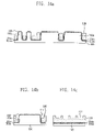
- FIG. 1 is a plan diagram illustrating finFETs according to some embodiments of the invention.
- FIGS. 2 through 11 are cross-sectional diagrams illustrating some exemplary processes for manufacturing the finFETs of FIG. 1 according to some embodiments of the invention.
- FIGS. 12–17 are cross-sectional diagrams illustrating more exemplary processes for manufacturing the finFETs of FIG. 1 according to some embodiments of the invention.
- FIG. 18 is a perspective diagram illustrating completed finFETs according to some embodiments of the invention.
- FIG. 1 is a plan diagram illustrating a finFET according to some embodiments of the invention, and illustrates an active region formed in cell area and peripheral area and a gate electrode.
- gate electrodes 112 a disposed on active regions 110 a are found in a cell area, and a gate electrode 112 b disposed on active regions 100 b are found in a peripheral area.
- the active regions 100 a and the gate electrodes 112 a in the cell area are positioned on the left of the drawing with a relatively small size, and the active regions 100 b and the gate electrode 112 b in the peripheral area are positioned on the right of the drawing with a relatively large size.
- FIGS. 2 to 11 are cross-sectional diagrams taken along the line I–I′ of FIG. 1 that illustrate some exemplary processes for manufacturing the finFETs of FIG. 1 according to some embodiments of the invention.
- a bulk semiconductor substrate 100 is provided, and a first oxide layer 102 is formed on the bulk semiconductor substrate 100 . Then, a first insulation layer is formed on the first oxide layer 102 .
- the first oxide layer 102 is preferably formed to a thickness of about 100 ⁇ , and the first insulation layer may be formed by depositing an SiN layer through LPCVD (Low Pressure Chemical Vapor Deposition) or PECVD (Plasma Enhanced Chemical Vapor Deposition), etc.
- a first photoresist pattern (not shown) for forming a fin as an active region is formed on the semiconductor substrate on which the first insulation layer was formed.
- the first insulation layer is etched until the first oxide layer 102 is exposed, by using the first photoresist pattern as a mask, to thus form a mask pattern.
- an exposed portion of the first oxide layer 102 is removed, and a second oxide layer 106 is formed on an entire face of the semiconductor substrate on which the mask pattern 104 was formed.
- the second oxide layer 106 is formed through a recently developed ISSG (in-situ steam generation) method.
- ISSG in-situ steam generation
- silicon dioxide grows not only on silicon but also on silicon nitride.
- a quality of oxide through the ISSG method is better than CVD (Chemical Vapor Deposition) oxide.
- the ISSG method is performed within a chamber having temperature of about 900°° C. about 1100° C.
- a surface of the semiconductor substrate 100 and upper part and side face of the mask pattern are oxidized.
- the second oxide layer 106 is formed to about 150 ⁇ on the surface of semiconductor substrate, and is formed to about 100 ⁇ on an upper part of the mask pattern 104 .
- the upper part of semiconductor substrate 100 adjacent to the lower part of the mask pattern 104 becomes rounded in shape.
- This rounded portion corresponds to the upper edge portion of a fin type active region formed in a subsequent process.
- the rounding-processed upper edge portion of active region prevents a leakage current caused in case of a low threshold voltage, and prevents a defect due to electric fields being overly concentrated onto the edge portion. This rounding process solves several problems caused by forming the edge portion in a pointed shape.
- the second oxide layer 106 provided on the surface of semiconductor substrate 100 and on an upper part of the mask pattern 104 is removed through an anisotropic etching process.
- the anisotropic etching process may employ a dry etching or plasma etching, etc.
- a second oxide layer 106 a formed on a side wall of the mask pattern 104 is not removed through the anisotropic etching process, and remains as a spacer in the mask pattern 104 , so as to protect the rounded portion of the substrate 100 processed through the ISSG method.
- the semiconductor substrate is etched by using the mask pattern 104 and the second oxide layer 106 a of spacer type as an etch mask, to form fin type active regions 100 a and 100 b .
- the active region 100 a and 100 b are formed to have a height of between about 2000 ⁇ to 3000 ⁇ , and preferably the height is about 2700 ⁇ .
- the etching process used to form the active regions 100 a and 100 b may employ a dry etching as the anisotropic etching process, etc.
- the spacer-type second oxide layer 106 a formed on the side wall of the mask pattern 104 is removed through an isotropic etching process.
- the etching process may employ a wet etching as the isotropic etching process.
- the rounded upper edge portion of active region 100 a and 100 b is exposed by the etching process that removes the spacer type second oxide layer 106 a.
- a third oxide layer 102 a is formed on an exposed surface of the semiconductor substrate.
- the third oxide layer 102 a is formed to a thickness of about 50 ⁇ .
- a nitride layer liner 104 a is formed on the third oxide layer 102 a and on the mask pattern 104 .
- the nitride layer liner 104 a may be formed up to a thickness of about 75 ⁇ by using deposition methods such as LPCVD (Low Pressure Chemical Vapor Deposition), PECVD (Plasma Enhanced Chemical Vapor Deposition), etc.
- the nitride layer liner 104 a is provided to protect the active regions 100 a and 100 b in the active region isolation process.
- a device isolation film 108 is formed over the semiconductor substrate where the nitride layer liner 104 a was formed.
- the device isolation film 108 fills the regions that separate the active regions 100 a and 100 b .
- the device isolation film 108 may be formed with an oxide deposition process using a high density plasma to a thickness of about 5000 ⁇ , which is thick enough to cover the semiconductor substrate.
- a polishing process such as CMP (Chemical Mechanical Polishing) is performed for the isolation film 108 by using the mask pattern 104 formed on the upper part of the active regions 100 a , 100 b as a polishing stop layer.
- CMP Chemical Mechanical Polishing
- the device isolation film 108 may be wet etched so that an upper height of the device isolation film 108 equals an upper height of the active region 100 a and 100 b . That is, the device isolation film 108 that is first formed to an upper height of the mask pattern 104 may be wet etched, by about 400 ⁇ , thereby resulting in the device isolation film 108 of FIG. 9 .
- a second insulation layer 104 b is formed on the resultant structure of FIG. 9 .
- the second insulation layer 104 b may be formed by depositing a nitride layer to a thickness of about 200 ⁇ , using LPCVD, PECVD, etc.
- the second insulation layer 104 b is removed from upper parts of the device isolation film 108 and the nitride layer liner 104 a .
- a portion of the second insulation layer 104 b remains on a sidewall of the mask pattern 104 .
- a spacer 104 c is formed on the upper edge portion of the active region.
- the spacer 104 c protects the rounded edge portion of active region 100 a and 100 b from being damaged in subsequent processes.
- the spacer 104 c may be formed by an etch back process.
- the active region 100 a and 100 b and the device isolation film 108 are formed on the cell area and on the peripheral area, as illustrated in FIG. 1 .
- FIGS. 12–17 are cross-sectional diagrams that illustrate some exemplary processes for manufacturing the finFETs of FIG. 1 according to other embodiments of the invention.
- FIGS. 12 a , 13 a , 14 a , 15 a , 16 a , and 17 a are cross-sectional diagrams taken along the line I–I′ of FIG. 1 .
- FIGS. 12 b , 13 b , 14 b , 15 b , 16 b , and 17 b are cross-sectional diagrams taken along the line II–II′ of FIG. 1 .
- FIGS. 12 c , 13 c , 14 c , 15 c , 16 c , and 17 c are cross-sectional diagrams taken along the line III–III′ of FIG. 1 .
- a second photoresist pattern 110 is formed on the semiconductor substrate to expose the portions of the cell area where the gate electrodes 112 a will be formed.
- the second photoresist pattern 110 is disposed to cover the peripheral area and the portion of the cell area where the gate electrodes are not formed.
- the device isolation film 108 is anisotropically etched by using the second photoresist pattern 110 , the mask pattern 104 , and the spacer 104 c as an etch mask, thus forming an opening part 111 in the cell area.
- the anisotropic etching process may employ an etching method such as a dry etching or a plasma etching.
- the opening part 111 is formed with a predetermined depth, exposing the nitride layer liner 104 a formed on the sidewalls of the active region that corresponds to a portion where the gate electrodes 112 a of the cell area will be formed.
- the opening part 111 is formed to a depth of about 1000 to 1500 ⁇ from an upper part of the active region.
- the spacer 104 c protects an upper edge portion of the active region 100 a and 100 b in etching the device isolation film 108 .
- the second photoresist pattern 110 is removed.
- an isotropic etching process is performed to remove portions of the device isolation film 108 from the cell area and from the peripheral area, using the mask pattern 104 and the spacer 104 c as an etch mask. Thereby, a portion of the device isolation film 108 existing between the nitride layer liner 104 a corresponding to the upper edge portion of active regions 100 a and 100 b and the spacer 104 c is removed.
- Such a process prevents particle generation caused by the subsequent removal process for the mask pattern 104 and the spacer 104 c.
- the mask pattern 104 and the spacer 104 c are removed, a portion of the nitride layer 104 a exposed in the opening part 111 is removed, and a portion of the nitride layer 104 a exposed in the peripheral area by the edge portion of active region 100 b is removed.
- an upper portion of the active region is exposed under a formed state of the first oxide layer 102
- the edge portion of active region and a portion of sidewalls are exposed under a formed state of the third oxide layer 102 a .
- the first oxide layer 102 and the third oxide layer 102 a formed on an upper part of the active region 100 a and 100 b and on a portion of the sidewalls function as a gate insulation layer.
- the following processes may be added. That is, the first oxide layer 102 and the third oxide layer 102 a , which are formed on the upper edge portion of active region including the cell area and the peripheral area and in partial sidewalls, are removed, and then a fourth oxide layer (not shown) is formed with about 70 ⁇ .
- the fourth oxide layer is formed to function as a gate insulation layer, because the first oxide layer 102 and the third oxide layer 102 a may be damaged during the above-described processes, causing some trouble for a normal operation as the gate insulation layer.
- a conductive layer 112 is formed on the semiconductor substrate where the gate insulation layer was formed.
- the conductive layer 112 is formed enough to sufficiently fill the opening part 111 and cover an upper part of the active regions 100 a and 100 b .
- the conductive layer 112 is preferably formed to a thickness of about 800 ⁇ on the upper part of the active regions.
- the conductive layer 112 may be formed of polysilicon material, or it may be formed of a metal layer or some other conductive material.
- a metal silicide layer 114 is formed over the semiconductor substrate where the conductive layer 112 was formed.
- the metal silicide layer 114 is preferably formed to a thickness of about 1000 ⁇ and may be, for example, tungsten silicide.
- an insulation layer 116 that functions as a gate capping layer may be formed over the semiconductor substrate where the metal silicide layer 114 was formed.
- the insulation layer 116 is preferably formed to a thickness of about 2000 ⁇ and may be, for example, formed of a nitride layer material.
- a third photoresist pattern (not shown) for forming a gate is formed on the semiconductor substrate on which the conductive layer 112 , the metal silicide layer 114 , and the insulation layer 116 as the capping layer were formed. Then, an anisotropic etching process is progressed by using the third photoresist pattern as an etching mask, to form a gate capping layer 116 a .
- the third photoresist pattern is removed through an ashing or stripping process, and the metal silicide layer 114 and the conductive layer 112 are anisotropically etched by using the gate capping layer 116 a as an etch mask and the device isolation film 108 as an etching stop layer, to thus form a gate electrode 112 a that includes a metal silicide layer 114 a.
- the gate electrode 112 a and the gate capping layer 116 a may alternatively be formed by sequentially anisotropic etching the insulation layer 116 as the gate capping layer, the metal silicide layer 114 and the conductive layer 112 , by using the third photoresist pattern as an etch mask and the device isolation film 108 as the etching stop layer.
- FIG. 18 is a perspective diagram illustrating completed finFETs according to the embodiments of the invention described above.
- the device isolation film 108 surrounds the active region 100 a formed on the semiconductor substrate 100 .
- the conductive layer 112 fills the opening part formed on the device isolation film 108 , and the gate electrode 112 a is formed in contact with a portion of sidewalls of the active region 100 a and covering an upper portion of the active region 100 a .
- the metal silicide layer 114 a and the gate capping layer 116 a are formed on an upper part of the gate electrode 112 a.
- the device isolation film 108 has a height that is equal to an upper part of the fin type active regions 100 a and 100 b , and a damascene method is employed, like forming the opening part 111 in the device isolation film 108 and filling the opening part 111 with the conductive layer 112 , etc.
- a damascene method is employed, like forming the opening part 111 in the device isolation film 108 and filling the opening part 111 with the conductive layer 112 , etc.
- the finFET is completed by forming source and drain regions through an ion implantation under interposing the gate electrode 112 a therebetween on the remaining portion of active region where the gate electrode 112 a and the gate capping layer 116 a are not formed.
- the finFET formed through the above processes may be desirably applied to a DRAM (Dynamic Random Access Memory) cell, it goes without saying that this is applicable to a formation of other memory devices such as a SRAM, etc.
- DRAM Dynamic Random Access Memory
- a method of forming a finFET prevents or substantially reduces problems such as a concentration of electric field or a leakage current, by rounding an upper edge portion of the fin type active region.
- the formation of a gate electrode using a damascene method provides process simplification, makes separation of the gate electrode easier, and prevents or reduces a short of the gate electrode.
- the etching amount is effectively reduced, lessening problems caused by too much etching by-product.
- Embodiments of the invention may be practiced in many ways. What follows are exemplary, non-limiting descriptions of some of these embodiments.
- a method of forming a finFET includes forming an active region of fin type under an exposure state of sidewalls on a semiconductor substrate; forming a gate insulation layer on an upper part of the active region and in the sidewalls, and then forming a device isolation film surrounding the active region by an upper height of the active region, and forming an opening part for partially exposing the sidewalls on the device isolation film; forming a gate electrode by filling the opening part with conductive layer with covering an upper portion of the active region; and forming source and drain between which the gate electrode is formed, on a portion where the gate electrode of active region is not formed.
- a method of forming a finFET includes forming an active region of fin type under an exposure state f sidewalls on a semiconductor substrate, and forming a device isolation film surrounding the active region by an upper height of the active region; forming an opening part for partially exposing the sidewalls of active region on a portion of the device isolation film; interposing a gate insulation layer in a portion of sidewalls exposed by the opening part and in an upper portion of the active region, and thus forming a gate electrode that fills the opening part and also covers an upper portion of the active region; and forming source and drain between which the gate electrode is formed, on a portion where the gate electrode is not formed in the active region.
- the active region is obtained by rounding an upper edge portion thereof, and it may be desirable to obtain the rounded edge portion of the active region through an oxide layer forming process using ISSG.
- a method of forming a finFET includes the following processes.
- a mask pattern of laminated structure having a first oxide layer and a first insulation layer of nitride layer material is formed by a first photoresist pattern to form a fin-type active region on a face of a bulk semiconductor substrate.
- a second oxide layer is formed through an ISSG process on a side face and an upper part of the semiconductor substrate and the mask pattern, thereby forming a rounded portion between the semiconductor substrate and a side face of the mask pattern.
- the second oxide layer except for the portion formed on the side face of the mask pattern, is removed. Then the semiconductor substrate is etched by using the mask pattern and the second oxide layer provided in the side face of the mask pattern as an mask, to thus form a fin-type active region.
- a rounded edge portion formed from the upper part of active region is exposed by removing the second oxide layer formed on the side face of mask pattern, and a third oxide layer is formed on an exposed portion of the semiconductor substrate including the active region.
- a nitride layer liner is formed on a face of semiconductor substrate where the third oxide layer was formed.
- a device isolating insulation layer fills a face of the semiconductor substrate where the nitride layer liner was formed.
- An isolation layer is formed by performing a planarization process through use of the mask pattern as a planarization stop layer.
- the device isolation film is etched back until an upper part of the active region is exposed by using the mask pattern as an etch mask.
- a second insulation layer of nitride layer material is formed with a predetermined thickness on a face of the semiconductor substrate, and is then etched back to expose an upper part of the device isolation film, thus forming a nitride layer spacer on a sidewall of the mask pattern.
- An opening part for partially exposing sidewalls of the active region is formed by etching the device isolation film to a predetermined depth by using a second photoresist pattern and the nitride layer spacer as a mask, the second photoresist pattern being for exposing only a portion where a gate of the cell area will be formed.
- the second photoresist pattern is removed, and an isotropic etching process is performed by using the nitride layer spacer as a mask, to remove a portion of the device isolation film formed between the nitride layer liner and the upper edge of active region.
- the mask pattern from an upper part of the active region, the nitride layer spacer, and the nitride layer liner of the exposed sidewall are removed.
- a polysilicon layer as a conductive layer having a given thickness is formed, filling the opening part, on a face of the semiconductor substrate from which the nitride layer liner was removed. Subsequently, a tungsten silicide layer and a nitride layer as a capping layer are sequentially formed on the conductive layer.
- the nitride layer as the capping layer, the tungsten silicide layer, and the polysilicon layer are sequentially etched by a third photoresist pattern until the device isolation film is exposed, to form a gate electrode and a gate capping layer.
- Source and drain regions between which the gate electrode is formed are formed on a portion of active region where the gate electrode is not formed.
- the method of forming the finFET may further include, removing the first oxide layer and the third oxide layer, which are formed on an upper part of the exposed active region and in the exposed sidewalls, to thus expose an upper part of active region and a portion of the sidewalls, after removing the mask pattern from the upper part of active region, the nitride layer spacer and the nitride layer liner of exposed sidewall; and forming a gate insulation layer on an upper part of the exposed active region and in a portion of the sidewalls.
- the method simplifies the separation of the gate electrode, substantially reduces problems caused by etching byproduct, prevents leakage current in the channel region, and prevents excessive electric field concentration onto an edge part of the active region.
Abstract
Description
Claims (26)
Applications Claiming Priority (2)
| Application Number | Priority Date | Filing Date | Title |
|---|---|---|---|
| KR2003-91716 | 2003-12-16 | ||
| KR10-2003-0091716A KR100513405B1 (en) | 2003-12-16 | 2003-12-16 | Method for forming fin field effect transistor |
Publications (2)
| Publication Number | Publication Date |
|---|---|
| US20050153490A1 US20050153490A1 (en) | 2005-07-14 |
| US7056781B2 true US7056781B2 (en) | 2006-06-06 |
Family
ID=34737877
Family Applications (1)
| Application Number | Title | Priority Date | Filing Date |
|---|---|---|---|
| US11/014,212 Active US7056781B2 (en) | 2003-12-16 | 2004-12-15 | Method of forming fin field effect transistor |
Country Status (2)
| Country | Link |
|---|---|
| US (1) | US7056781B2 (en) |
| KR (1) | KR100513405B1 (en) |
Cited By (26)
| Publication number | Priority date | Publication date | Assignee | Title |
|---|---|---|---|---|
| US20070020879A1 (en) * | 2005-07-19 | 2007-01-25 | Samsung Electronics Co., Ltd | Method of forming an isolation layer and method of manufacturing a field effect transistor using the same |
| US20070034925A1 (en) * | 2003-06-30 | 2007-02-15 | Deok-Hyung Lee | Fin-field effect transistors (Fin-FETs) having protection layers |
| US20070048947A1 (en) * | 2003-08-14 | 2007-03-01 | Lee Deok H | Multi-structured Si-fin and method of manufacture |
| US20080064154A1 (en) * | 2006-09-13 | 2008-03-13 | Haller Gordon A | Process flow for metal gate access device |
| US20080081420A1 (en) * | 2006-09-29 | 2008-04-03 | Hynix Semiconductor Inc. | Method for fabricating fin transistor |
| US20080185650A1 (en) * | 2007-02-01 | 2008-08-07 | Taiwan Semiconductor Manufacturing Co., Ltd. | FinFET for device characterization |
| US20080237684A1 (en) * | 2007-03-26 | 2008-10-02 | Michael Specht | Method of manufacturing a nanowire transistor, a nanowire transistor structure, a nanowire transistor field |
| US20100320572A1 (en) * | 2009-06-22 | 2010-12-23 | Taiwan Semiconductor Manufacturing Co., Ltd. | Thin-Body Bipolar Device |
| US20110021010A1 (en) * | 2009-07-27 | 2011-01-27 | International Business Machines Corporation | Method for double pattern density |
| US20110097863A1 (en) * | 2009-10-27 | 2011-04-28 | Taiwan Semiconductor Manufacturing Company, Ltd. | Cross OD FinFET Patterning |
| US8436405B2 (en) | 2010-06-30 | 2013-05-07 | Taiwan Semiconductor Manufacturing Company, Ltd. | ROM cell circuit for FinFET devices |
| US8633076B2 (en) | 2010-11-23 | 2014-01-21 | Taiwan Semiconductor Manufacturing Company, Ltd. | Method for adjusting fin width in integrated circuitry |
| US8697522B2 (en) | 2011-07-05 | 2014-04-15 | International Business Machines Corporation | Bulk finFET with uniform height and bottom isolation |
| US8703571B2 (en) | 2009-01-28 | 2014-04-22 | Taiwan Semiconductor Manufacturing Company, Ltd. | Methods of fabricating bipolar junction transistors having a fin |
| US8878309B1 (en) | 2013-08-22 | 2014-11-04 | Samsung Electronics Co., Ltd. | Semiconductor device having 3D channels, and methods of fabricating semiconductor devices having 3D channels |
| US8927371B2 (en) | 2009-04-01 | 2015-01-06 | Taiwan Semiconductor Manufacturing Company, Ltd. | High-mobility multiple-gate transistor with improved on-to-off current ratio |
| US8942030B2 (en) | 2010-06-25 | 2015-01-27 | Taiwan Semiconductor Manufacturing Company, Ltd. | Structure and method for SRAM cell circuit |
| US9130058B2 (en) | 2010-07-26 | 2015-09-08 | Taiwan Semiconductor Manufacturing Company, Ltd. | Forming crown active regions for FinFETs |
| US9202915B2 (en) | 2009-10-30 | 2015-12-01 | Taiwan Semiconductor Manufacturing Company, Ltd. | Method of forming epi film in substrate trench |
| US9379106B2 (en) | 2013-08-22 | 2016-06-28 | Samsung Electronics Co., Ltd. | Semiconductor devices having 3D channels, and methods of fabricating semiconductor devices having 3D channels |
| US9431478B2 (en) | 2014-04-30 | 2016-08-30 | Samsung Electronics Co., Ltd. | Semiconductor device and method of fabricating the same |
| US9472550B2 (en) | 2010-11-23 | 2016-10-18 | Taiwan Semiconductor Manufacturing Company, Ltd. | Adjusted fin width in integrated circuitry |
| US9653593B2 (en) | 2009-09-29 | 2017-05-16 | Taiwan Semiconductor Manufacturing Company, Ltd. | Method of fabricating FinFET device and structure thereof |
| US9905480B1 (en) * | 2016-11-15 | 2018-02-27 | Nuvoton Technology Corporation | Semiconductor devices and methods for forming the same |
| US10084085B2 (en) | 2015-06-11 | 2018-09-25 | Taiwan Semiconductor Manufacturing Co., Ltd. | Fin field effect transistor (FinFET) device structure with stop layer and method for forming the same |
| US10840356B2 (en) * | 2017-08-31 | 2020-11-17 | Taiwan Semiconductor Manufacturing Company, Ltd. | FinFET device and method of forming same |
Families Citing this family (150)
| Publication number | Priority date | Publication date | Assignee | Title |
|---|---|---|---|---|
| KR100587672B1 (en) * | 2004-02-02 | 2006-06-08 | 삼성전자주식회사 | Method for forming FINFET using damascene process |
| KR100605104B1 (en) * | 2004-05-04 | 2006-07-26 | 삼성전자주식회사 | Fin Field Effect Transistor Device And Method Of Fabricating The Same |
| US7244640B2 (en) * | 2004-10-19 | 2007-07-17 | Taiwan Semiconductor Manufacturing Company, Ltd. | Method for fabricating a body contact in a Finfet structure and a device including the same |
| KR100698068B1 (en) * | 2004-12-30 | 2007-03-23 | 동부일렉트로닉스 주식회사 | A fin-FET and a method for fabricating the same |
| TWI240989B (en) * | 2005-01-17 | 2005-10-01 | Powerchip Semiconductor Corp | Method for forming trench gate dielectric layer |
| US20070018239A1 (en) * | 2005-07-20 | 2007-01-25 | International Business Machines Corporation | Sea-of-fins structure on a semiconductor substrate and method of fabrication |
| US7381649B2 (en) | 2005-07-29 | 2008-06-03 | Taiwan Semiconductor Manufacturing Company, Ltd. | Structure for a multiple-gate FET device and a method for its fabrication |
| KR100675288B1 (en) | 2005-11-04 | 2007-01-29 | 삼성전자주식회사 | Fabrication methods of semiconductor devices having multiple channel transistors and semiconductor devices fabricated thereby |
| KR100653712B1 (en) | 2005-11-14 | 2006-12-05 | 삼성전자주식회사 | Semiconductor devices with a device isolation layer having a substantially same top surface compared with a top surface of an active region in a finfet and methods of forming the same |
| KR100763330B1 (en) * | 2005-12-14 | 2007-10-04 | 삼성전자주식회사 | Isolation method defining active fins, method for fabricating semiconductor device using the same, and semiconductor device fabricated thereby |
| KR100743655B1 (en) * | 2006-06-29 | 2007-07-30 | 주식회사 하이닉스반도체 | Method for forming saddle fin transistor |
| US8946811B2 (en) | 2006-07-10 | 2015-02-03 | Taiwan Semiconductor Manufacturing Company, Ltd. | Body-tied, strained-channel multi-gate device and methods of manufacturing same |
| KR100827656B1 (en) * | 2006-08-11 | 2008-05-07 | 삼성전자주식회사 | Transistor having recess channel structure and fin structure, semicoductor device employing the transistor, and method of frabication the semiconductor device |
| KR100814391B1 (en) * | 2006-10-10 | 2008-03-18 | 삼성전자주식회사 | Method of operating dram device including fin transistor and dram device |
| US8286114B2 (en) | 2007-04-18 | 2012-10-09 | Taiwan Semiconductor Manufacturing Company, Ltd. | 3-dimensional device design layout |
| US7560785B2 (en) * | 2007-04-27 | 2009-07-14 | Taiwan Semiconductor Manufacturing Company, Ltd. | Semiconductor device having multiple fin heights |
| US8927353B2 (en) | 2007-05-07 | 2015-01-06 | Taiwan Semiconductor Manufacturing Co., Ltd. | Fin field effect transistor and method of forming the same |
| US8174073B2 (en) | 2007-05-30 | 2012-05-08 | Taiwan Semiconductor Manufacturing Co., Ltd. | Integrated circuit structures with multiple FinFETs |
| US8237201B2 (en) | 2007-05-30 | 2012-08-07 | Taiwan Semiconductor Manufacturing Company, Ltd. | Layout methods of integrated circuits having unit MOS devices |
| US8883597B2 (en) * | 2007-07-31 | 2014-11-11 | Taiwan Semiconductor Manufacturing Company, Ltd. | Method of fabrication of a FinFET element |
| US7910994B2 (en) * | 2007-10-15 | 2011-03-22 | Taiwan Semiconductor Manufacturing Company, Ltd. | System and method for source/drain contact processing |
| US7939889B2 (en) * | 2007-10-16 | 2011-05-10 | Taiwan Semiconductor Manufacturing Company, Ltd. | Reducing resistance in source and drain regions of FinFETs |
| US8187948B2 (en) | 2008-02-18 | 2012-05-29 | Taiwan Semiconductor Manufacturing Company, Ltd. | Hybrid gap-fill approach for STI formation |
| US8106459B2 (en) | 2008-05-06 | 2012-01-31 | Taiwan Semiconductor Manufacturing Company, Ltd. | FinFETs having dielectric punch-through stoppers |
| US8048723B2 (en) * | 2008-12-05 | 2011-11-01 | Taiwan Semiconductor Manufacturing Company, Ltd. | Germanium FinFETs having dielectric punch-through stoppers |
| US8283231B2 (en) | 2008-06-11 | 2012-10-09 | Taiwan Semiconductor Manufacturing Company, Ltd. | finFET drive strength modification |
| US8093111B2 (en) * | 2008-07-29 | 2012-01-10 | Hynix Semiconductor Inc. | Semiconductor device including partial silicon on insulator fin structure and method for fabricating the same |
| US8153493B2 (en) * | 2008-08-28 | 2012-04-10 | Taiwan Semiconductor Manufacturing Company, Ltd. | FinFET process compatible native transistor |
| US7915112B2 (en) * | 2008-09-23 | 2011-03-29 | Taiwan Semiconductor Manufacturing Company, Ltd. | Metal gate stress film for mobility enhancement in FinFET device |
| US8048813B2 (en) * | 2008-12-01 | 2011-11-01 | Taiwan Semiconductor Manufacturing Company, Ltd. | Method of reducing delamination in the fabrication of small-pitch devices |
| US8144501B2 (en) * | 2008-12-29 | 2012-03-27 | Taiwan Semiconductor Manufacturing Co., Ltd. | Read/write margin improvement in SRAM design using dual-gate transistors |
| US8058692B2 (en) | 2008-12-29 | 2011-11-15 | Taiwan Semiconductor Manufacturing Company, Ltd. | Multiple-gate transistors with reverse T-shaped fins |
| US20100167506A1 (en) * | 2008-12-31 | 2010-07-01 | Taiwan Semiconductor Manufacturing Co., Ltd. | Inductive plasma doping |
| US8263462B2 (en) * | 2008-12-31 | 2012-09-11 | Taiwan Semiconductor Manufacturing Company, Ltd. | Dielectric punch-through stoppers for forming FinFETs having dual fin heights |
| US7862962B2 (en) * | 2009-01-20 | 2011-01-04 | Taiwan Semiconductor Manufacturing Company, Ltd. | Integrated circuit layout design |
| US7989355B2 (en) * | 2009-02-12 | 2011-08-02 | Taiwan Semiconductor Manufacturing Company, Ltd. | Method of pitch halving |
| US9159808B2 (en) * | 2009-01-26 | 2015-10-13 | Taiwan Semiconductor Manufacturing Company, Ltd. | Selective etch-back process for semiconductor devices |
| US8400813B2 (en) * | 2009-02-10 | 2013-03-19 | Taiwan Semiconductor Manufacturing Company, Ltd. | One-time programmable fuse with ultra low programming current |
| US8331068B2 (en) | 2009-02-19 | 2012-12-11 | Taiwan Semiconductor Manufacturing Company, Ltd. | ESD protection for FinFETs |
| US8305829B2 (en) * | 2009-02-23 | 2012-11-06 | Taiwan Semiconductor Manufacturing Company, Ltd. | Memory power gating circuit for controlling internal voltage of a memory array, system and method for controlling the same |
| US8293616B2 (en) | 2009-02-24 | 2012-10-23 | Taiwan Semiconductor Manufacturing Company, Ltd. | Methods of fabrication of semiconductor devices with low capacitance |
| US8305790B2 (en) * | 2009-03-16 | 2012-11-06 | Taiwan Semiconductor Manufacturing Company, Ltd. | Electrical anti-fuse and related applications |
| US8319311B2 (en) * | 2009-03-16 | 2012-11-27 | Taiwan Semiconductor Manufacturing Company, Ltd. | Hybrid STI gap-filling approach |
| US8004042B2 (en) | 2009-03-20 | 2011-08-23 | Taiwan Semiconductor Manufacturing Company, Ltd. | Static random access memory (SRAM) cell and method for forming same |
| US8957482B2 (en) * | 2009-03-31 | 2015-02-17 | Taiwan Semiconductor Manufacturing Company, Ltd. | Electrical fuse and related applications |
| US8816391B2 (en) * | 2009-04-01 | 2014-08-26 | Taiwan Semiconductor Manufacturing Company, Ltd. | Source/drain engineering of devices with high-mobility channels |
| US8912602B2 (en) * | 2009-04-14 | 2014-12-16 | Taiwan Semiconductor Manufacturing Company, Ltd. | FinFETs and methods for forming the same |
| US8457930B2 (en) * | 2009-04-15 | 2013-06-04 | James Schroeder | Personalized fit and functional designed medical prostheses and surgical instruments and methods for making |
| US8053299B2 (en) | 2009-04-17 | 2011-11-08 | Taiwan Semiconductor Manufacturing Company, Ltd. | Method of fabrication of a FinFET element |
| US7919335B2 (en) * | 2009-04-20 | 2011-04-05 | Taiwan Semiconductor Manufacturing Co., Ltd. | Formation of shallow trench isolation using chemical vapor etch |
| US9054194B2 (en) | 2009-04-29 | 2015-06-09 | Taiwan Semiconductor Manufactruing Company, Ltd. | Non-planar transistors and methods of fabrication thereof |
| US8455860B2 (en) | 2009-04-30 | 2013-06-04 | Taiwan Semiconductor Manufacturing Company, Ltd. | Reducing source/drain resistance of III-V based transistors |
| US9768305B2 (en) * | 2009-05-29 | 2017-09-19 | Taiwan Semiconductor Manufacturing Company, Ltd. | Gradient ternary or quaternary multiple-gate transistor |
| US8617976B2 (en) * | 2009-06-01 | 2013-12-31 | Taiwan Semiconductor Manufacturing Company, Ltd. | Source/drain re-growth for manufacturing III-V based transistors |
| US8173499B2 (en) | 2009-06-12 | 2012-05-08 | Taiwan Semiconductor Manufacturing Co., Ltd. | Method of fabricating a gate stack integration of complementary MOS device |
| US8461015B2 (en) * | 2009-07-08 | 2013-06-11 | Taiwan Semiconductor Manufacturing Company, Ltd. | STI structure and method of forming bottom void in same |
| US8472227B2 (en) * | 2010-01-27 | 2013-06-25 | Taiwan Semiconductor Manufacturing Company, Ltd. | Integrated circuits and methods for forming the same |
| US8980719B2 (en) | 2010-04-28 | 2015-03-17 | Taiwan Semiconductor Manufacturing Company, Ltd. | Methods for doping fin field-effect transistors |
| US9484462B2 (en) | 2009-09-24 | 2016-11-01 | Taiwan Semiconductor Manufacturing Company, Ltd. | Fin structure of fin field effect transistor |
| US8264021B2 (en) * | 2009-10-01 | 2012-09-11 | Taiwan Semiconductor Manufacturing Company, Ltd. | Finfets and methods for forming the same |
| US8759943B2 (en) | 2010-10-08 | 2014-06-24 | Taiwan Semiconductor Manufacturing Company, Ltd. | Transistor having notched fin structure and method of making the same |
| US8264032B2 (en) * | 2009-09-01 | 2012-09-11 | Taiwan Semiconductor Manufacturing Company, Ltd. | Accumulation type FinFET, circuits and fabrication method thereof |
| US8482073B2 (en) * | 2010-03-25 | 2013-07-09 | Taiwan Semiconductor Manufacturing Company, Ltd. | Integrated circuit including FINFETs and methods for forming the same |
| US8114721B2 (en) * | 2009-12-15 | 2012-02-14 | Taiwan Semiconductor Manufacturing Company, Ltd. | Method of controlling gate thickness in forming FinFET devices |
| US8497528B2 (en) | 2010-05-06 | 2013-07-30 | Taiwan Semiconductor Manufacturing Company, Ltd. | Method for fabricating a strained structure |
| US8629478B2 (en) * | 2009-07-31 | 2014-01-14 | Taiwan Semiconductor Manufacturing Company, Ltd. | Fin structure for high mobility multiple-gate transistor |
| US8623728B2 (en) * | 2009-07-28 | 2014-01-07 | Taiwan Semiconductor Manufacturing Company, Ltd. | Method for forming high germanium concentration SiGe stressor |
| US8298925B2 (en) | 2010-11-08 | 2012-10-30 | Taiwan Semiconductor Manufacturing Company, Ltd. | Mechanisms for forming ultra shallow junction |
| US8440517B2 (en) | 2010-10-13 | 2013-05-14 | Taiwan Semiconductor Manufacturing Company, Ltd. | FinFET and method of fabricating the same |
| US8187928B2 (en) | 2010-09-21 | 2012-05-29 | Taiwan Semiconductor Manufacturing Company, Ltd. | Methods of forming integrated circuits |
| US9245805B2 (en) | 2009-09-24 | 2016-01-26 | Taiwan Semiconductor Manufacturing Company, Ltd. | Germanium FinFETs with metal gates and stressors |
| US8362575B2 (en) | 2009-09-29 | 2013-01-29 | Taiwan Semiconductor Manufacturing Company, Ltd. | Controlling the shape of source/drain regions in FinFETs |
| US8519481B2 (en) | 2009-10-14 | 2013-08-27 | Taiwan Semiconductor Manufacturing Company, Ltd. | Voids in STI regions for forming bulk FinFETs |
| US9112052B2 (en) | 2009-10-14 | 2015-08-18 | Taiwan Semiconductor Manufacturing Company, Ltd. | Voids in STI regions for forming bulk FinFETs |
| US8610240B2 (en) * | 2009-10-16 | 2013-12-17 | Taiwan Semiconductor Manufacturing Company, Ltd. | Integrated circuit with multi recessed shallow trench isolation |
| US20110097867A1 (en) * | 2009-10-22 | 2011-04-28 | Taiwan Semiconductor Manufacturing Company, Ltd. | Method of controlling gate thicknesses in forming fusi gates |
| US9953885B2 (en) * | 2009-10-27 | 2018-04-24 | Taiwan Semiconductor Manufacturing Company, Ltd. | STI shape near fin bottom of Si fin in bulk FinFET |
| US8653608B2 (en) | 2009-10-27 | 2014-02-18 | Taiwan Semiconductor Manufacturing Company, Ltd. | FinFET design with reduced current crowding |
| US8592918B2 (en) * | 2009-10-28 | 2013-11-26 | Taiwan Semiconductor Manufacturing Company, Ltd. | Forming inter-device STI regions and intra-device STI regions using different dielectric materials |
| US8637135B2 (en) | 2009-11-18 | 2014-01-28 | Taiwan Semiconductor Manufacturing Company, Ltd. | Non-uniform semiconductor device active area pattern formation |
| US8445340B2 (en) * | 2009-11-19 | 2013-05-21 | Taiwan Semiconductor Manufacturing Company, Ltd. | Sacrificial offset protection film for a FinFET device |
| US8941153B2 (en) * | 2009-11-20 | 2015-01-27 | Taiwan Semiconductor Manufacturing Company, Ltd. | FinFETs with different fin heights |
| US8426923B2 (en) * | 2009-12-02 | 2013-04-23 | Taiwan Semiconductor Manufacturing Company, Ltd. | Multiple-gate semiconductor device and method |
| US8373238B2 (en) | 2009-12-03 | 2013-02-12 | Taiwan Semiconductor Manufacturing Company, Ltd. | FinFETs with multiple Fin heights |
| US9087725B2 (en) | 2009-12-03 | 2015-07-21 | Taiwan Semiconductor Manufacturing Company, Ltd. | FinFETs with different fin height and EPI height setting |
| US8258572B2 (en) * | 2009-12-07 | 2012-09-04 | Taiwan Semiconductor Manufacturing Company, Ltd. | SRAM structure with FinFETs having multiple fins |
| US9117905B2 (en) * | 2009-12-22 | 2015-08-25 | Taiwan Semiconductor Manufacturing Company, Ltd. | Method for incorporating impurity element in EPI silicon process |
| US8813014B2 (en) * | 2009-12-30 | 2014-08-19 | Taiwan Semiconductor Manufacturing Co., Ltd. | Semiconductor device and method for making the same using semiconductor fin density design rules |
| US8557692B2 (en) * | 2010-01-12 | 2013-10-15 | Taiwan Semiconductor Manufacturing Company, Ltd. | FinFET LDD and source drain implant technique |
| US9040393B2 (en) | 2010-01-14 | 2015-05-26 | Taiwan Semiconductor Manufacturing Company, Ltd. | Method of forming semiconductor structure |
| US8709928B2 (en) * | 2010-01-19 | 2014-04-29 | Taiwan Semiconductor Manufacturing Co., Ltd. | Semiconductor fin device and method for forming the same using high tilt angle implant |
| US8513107B2 (en) * | 2010-01-26 | 2013-08-20 | Taiwan Semiconductor Manufacturing Co., Ltd. | Replacement gate FinFET devices and methods for forming the same |
| US9362290B2 (en) * | 2010-02-08 | 2016-06-07 | Taiwan Semiconductor Manufacturing Company, Ltd. | Memory cell layout |
| US8395195B2 (en) | 2010-02-09 | 2013-03-12 | Taiwan Semiconductor Manufacturing Company, Ltd. | Bottom-notched SiGe FinFET formation using condensation |
| US8785286B2 (en) | 2010-02-09 | 2014-07-22 | Taiwan Semiconductor Manufacturing Company, Ltd. | Techniques for FinFET doping |
| US8362572B2 (en) | 2010-02-09 | 2013-01-29 | Taiwan Semiconductor Manufacturing Co., Ltd. | Lower parasitic capacitance FinFET |
| US8310013B2 (en) * | 2010-02-11 | 2012-11-13 | Taiwan Semiconductor Manufacturing Company, Ltd. | Method of fabricating a FinFET device |
| US8034677B2 (en) | 2010-02-25 | 2011-10-11 | Taiwan Semiconductor Manufacturing Co., Ltd. | Integrated method for forming high-k metal gate FinFET devices |
| US8263451B2 (en) * | 2010-02-26 | 2012-09-11 | Taiwan Semiconductor Manufacturing Company, Ltd. | Epitaxy profile engineering for FinFETs |
| US8937353B2 (en) | 2010-03-01 | 2015-01-20 | Taiwan Semiconductor Manufacturing Co., Ltd. | Dual epitaxial process for a finFET device |
| US8278179B2 (en) * | 2010-03-09 | 2012-10-02 | Taiwan Semiconductor Manufacturing Co., Ltd. | LDD epitaxy for FinFETs |
| US8675397B2 (en) | 2010-06-25 | 2014-03-18 | Taiwan Semiconductor Manufacturing Company, Ltd. | Cell structure for dual-port SRAM |
| US8399931B2 (en) | 2010-06-30 | 2013-03-19 | Taiwan Semiconductor Manufacturing Company, Ltd. | Layout for multiple-fin SRAM cell |
| US9312179B2 (en) * | 2010-03-17 | 2016-04-12 | Taiwan-Semiconductor Manufacturing Co., Ltd. | Method of making a finFET, and finFET formed by the method |
| US8609495B2 (en) | 2010-04-08 | 2013-12-17 | Taiwan Semiconductor Manufacturing Company, Ltd. | Hybrid gate process for fabricating finfet device |
| US8881084B2 (en) | 2010-05-14 | 2014-11-04 | Taiwan Semiconductor Manufacturing Company, Ltd. | FinFET boundary optimization |
| US8729627B2 (en) | 2010-05-14 | 2014-05-20 | Taiwan Semiconductor Manufacturing Company, Ltd. | Strained channel integrated circuit devices |
| US8621398B2 (en) | 2010-05-14 | 2013-12-31 | Taiwan Semiconductor Manufacturing Company, Ltd. | Automatic layout conversion for FinFET device |
| US8455929B2 (en) | 2010-06-30 | 2013-06-04 | Taiwan Semiconductor Manufacturing Company, Ltd. | Formation of III-V based devices on semiconductor substrates |
| US8278173B2 (en) | 2010-06-30 | 2012-10-02 | Taiwan Semiconductor Manufacturing Company, Ltd. | Method of fabricating gate structures |
| US8796759B2 (en) | 2010-07-15 | 2014-08-05 | Taiwan Semiconductor Manufacturing Company, Ltd. | Fin-like field effect transistor (FinFET) device and method of manufacturing same |
| US8278196B2 (en) | 2010-07-21 | 2012-10-02 | Taiwan Semiconductor Manufacturing Company, Ltd. | High surface dopant concentration semiconductor device and method of fabricating |
| US8373229B2 (en) | 2010-08-30 | 2013-02-12 | Taiwan Semiconductor Manufacturing Company, Ltd. | Gate controlled bipolar junction transistor on fin-like field effect transistor (FinFET) structure |
| US8258848B2 (en) | 2010-09-07 | 2012-09-04 | Taiwan Semiconductor Manufacturing Co., Ltd. | Level shifter |
| US8659072B2 (en) | 2010-09-24 | 2014-02-25 | Taiwan Semiconductor Manufacturing Company, Ltd. | Series FinFET implementation schemes |
| US8062963B1 (en) | 2010-10-08 | 2011-11-22 | Taiwan Semiconductor Manufacturing Company, Ltd. | Method of fabricating a semiconductor device having an epitaxy region |
| US8367498B2 (en) | 2010-10-18 | 2013-02-05 | Taiwan Semiconductor Manufacturing Company, Ltd. | Fin-like field effect transistor (FinFET) device and method of manufacturing same |
| US9166022B2 (en) | 2010-10-18 | 2015-10-20 | Taiwan Semiconductor Manufacturing Company, Ltd. | Fin-like field effect transistor (FinFET) device and method of manufacturing same |
| US8603924B2 (en) | 2010-10-19 | 2013-12-10 | Taiwan Semiconductor Manufacturing Company, Ltd. | Methods of forming gate dielectric material |
| US8338305B2 (en) | 2010-10-19 | 2012-12-25 | Taiwan Semiconductor Manufacturing Company, Ltd. | Multi-fin device by self-aligned castle fin formation |
| US9048181B2 (en) | 2010-11-08 | 2015-06-02 | Taiwan Semiconductor Manufacturing Company, Ltd. | Mechanisms for forming ultra shallow junction |
| US8769446B2 (en) | 2010-11-12 | 2014-07-01 | Taiwan Semiconductor Manufacturing Company, Ltd. | Method and device for increasing fin device density for unaligned fins |
| US8486769B2 (en) | 2010-11-19 | 2013-07-16 | Taiwan Semiconductor Manufacturing Company, Ltd. | Method for forming metrology structures from fins in integrated circuitry |
| US8525267B2 (en) | 2010-11-23 | 2013-09-03 | Taiwan Semiconductor Manufacturing Company, Ltd. | Device and method for forming Fins in integrated circuitry |
| US8877602B2 (en) | 2011-01-25 | 2014-11-04 | Taiwan Semiconductor Manufacturing Company, Ltd. | Mechanisms of doping oxide for forming shallow trench isolation |
| US8592915B2 (en) | 2011-01-25 | 2013-11-26 | Taiwan Semiconductor Manufacturing Company, Ltd. | Doped oxide for shallow trench isolation (STI) |
| US8482952B2 (en) | 2011-02-17 | 2013-07-09 | Taiwan Semiconductor Manufacturing Company, Ltd. | One time programming bit cell |
| US8431453B2 (en) | 2011-03-31 | 2013-04-30 | Taiwan Semiconductor Manufacturing Company, Ltd. | Plasma doping to reduce dielectric loss during removal of dummy layers in a gate structure |
| US8853013B2 (en) * | 2011-08-19 | 2014-10-07 | United Microelectronics Corp. | Method for fabricating field effect transistor with fin structure |
| US8796124B2 (en) | 2011-10-25 | 2014-08-05 | Taiwan Semiconductor Manufacturing Company, Ltd. | Doping method in 3D semiconductor device |
| JP5816560B2 (en) * | 2012-01-10 | 2015-11-18 | ルネサスエレクトロニクス株式会社 | Semiconductor device and manufacturing method thereof |
| KR102013842B1 (en) | 2013-02-08 | 2019-08-26 | 삼성전자주식회사 | Method of manufacturing semiconductor device |
| US9159833B2 (en) * | 2013-11-26 | 2015-10-13 | Taiwan Semiconductor Manufacturing Company, Ltd. | Fin structure of semiconductor device |
| US9136356B2 (en) * | 2014-02-10 | 2015-09-15 | Taiwan Semiconductor Manufacturing Co., Ltd. | Non-planar field effect transistor having a semiconductor fin and method for manufacturing |
| US9324619B2 (en) * | 2014-08-25 | 2016-04-26 | Samsung Electronics Co., Ltd. | Semiconductor device and method of fabricating the same |
| KR102265271B1 (en) | 2015-01-14 | 2021-06-17 | 삼성전자주식회사 | Semiconductor devices and method for forming the same |
| KR102287398B1 (en) * | 2015-01-14 | 2021-08-06 | 삼성전자주식회사 | Semiconductor device |
| TWI637514B (en) * | 2015-04-24 | 2018-10-01 | 聯華電子股份有限公司 | Semiconductor structure and manufacturing method thereof |
| US9515089B1 (en) | 2015-05-14 | 2016-12-06 | International Business Machines Corporation | Bulk fin formation with vertical fin sidewall profile |
| US9673207B2 (en) * | 2015-08-20 | 2017-06-06 | Sandisk Technologies Llc | Shallow trench isolation trenches and methods for NAND memory |
| US9754993B2 (en) * | 2015-08-31 | 2017-09-05 | Taiwan Semiconductor Manufacturing Company, Ltd. | Deep trench isolations and methods of forming the same |
| CN107180784B (en) * | 2016-03-09 | 2020-03-10 | 中芯国际集成电路制造(上海)有限公司 | Semiconductor structure and forming method thereof |
| CN108807532B (en) * | 2017-04-28 | 2021-07-06 | 中芯国际集成电路制造(上海)有限公司 | Semiconductor device and method for manufacturing the same |
| CN108933105B (en) * | 2017-05-24 | 2020-11-03 | 中芯国际集成电路制造(上海)有限公司 | Semiconductor structure and forming method thereof |
| US10692769B2 (en) * | 2017-08-29 | 2020-06-23 | Taiwan Semiconductor Manufacturing Co., Ltd | Fin critical dimension loading optimization |
| US10410928B2 (en) * | 2017-11-28 | 2019-09-10 | International Business Machines Corporation | Homogeneous densification of fill layers for controlled reveal of vertical fins |
| TWI754722B (en) | 2018-02-13 | 2022-02-11 | 聯華電子股份有限公司 | Layout of semiconductor device, semiconductor device and method of forming the same |
| CN110581138B (en) * | 2018-06-08 | 2021-07-13 | 联华电子股份有限公司 | Semiconductor element and manufacturing method thereof |
| US10622481B2 (en) * | 2018-08-07 | 2020-04-14 | United Microelectronics Corp. | Method of rounding corners of a fin |
| US11094695B2 (en) * | 2019-05-17 | 2021-08-17 | Taiwan Semiconductor Manufacturing Co., Ltd. | Integrated circuit device and method of forming the same |
Citations (6)
| Publication number | Priority date | Publication date | Assignee | Title |
|---|---|---|---|---|
| US6417047B1 (en) | 1999-09-20 | 2002-07-09 | Kabushiki Kaisha Toshiba | Manufacturing method of a non-volatile semiconductor memory device having isolation regions |
| US6548859B2 (en) | 2000-08-28 | 2003-04-15 | Mitsubishi Denki Kabushiki Kaisha | MOS semiconductor device and method of manufacturing the same |
| US20030122186A1 (en) | 2001-03-13 | 2003-07-03 | Nat'l. Inst. Of Advanced Indust'l Sci. And Tech. | Double-gate field-effect transistor, integrated circuit using the transistor and method of manufacturing the same |
| US6642090B1 (en) | 2002-06-03 | 2003-11-04 | International Business Machines Corporation | Fin FET devices from bulk semiconductor and method for forming |
| US6846734B2 (en) * | 2002-11-20 | 2005-01-25 | International Business Machines Corporation | Method and process to make multiple-threshold metal gates CMOS technology |
| US6855588B1 (en) * | 2003-10-07 | 2005-02-15 | United Microelectronics Corp. | Method of fabricating a double gate MOSFET device |
-
2003
- 2003-12-16 KR KR10-2003-0091716A patent/KR100513405B1/en active IP Right Grant
-
2004
- 2004-12-15 US US11/014,212 patent/US7056781B2/en active Active
Patent Citations (6)
| Publication number | Priority date | Publication date | Assignee | Title |
|---|---|---|---|---|
| US6417047B1 (en) | 1999-09-20 | 2002-07-09 | Kabushiki Kaisha Toshiba | Manufacturing method of a non-volatile semiconductor memory device having isolation regions |
| US6548859B2 (en) | 2000-08-28 | 2003-04-15 | Mitsubishi Denki Kabushiki Kaisha | MOS semiconductor device and method of manufacturing the same |
| US20030122186A1 (en) | 2001-03-13 | 2003-07-03 | Nat'l. Inst. Of Advanced Indust'l Sci. And Tech. | Double-gate field-effect transistor, integrated circuit using the transistor and method of manufacturing the same |
| US6642090B1 (en) | 2002-06-03 | 2003-11-04 | International Business Machines Corporation | Fin FET devices from bulk semiconductor and method for forming |
| US6846734B2 (en) * | 2002-11-20 | 2005-01-25 | International Business Machines Corporation | Method and process to make multiple-threshold metal gates CMOS technology |
| US6855588B1 (en) * | 2003-10-07 | 2005-02-15 | United Microelectronics Corp. | Method of fabricating a double gate MOSFET device |
Non-Patent Citations (1)
| Title |
|---|
| Park et al., "A 40nm Body-Tied FinFET (OMEGA MOSFET) using Bulk Si Wafer" Physica E, vol. 19, Issues 1-2, pp. 6-12 (Jul. 2003). |
Cited By (50)
| Publication number | Priority date | Publication date | Assignee | Title |
|---|---|---|---|---|
| US20070034925A1 (en) * | 2003-06-30 | 2007-02-15 | Deok-Hyung Lee | Fin-field effect transistors (Fin-FETs) having protection layers |
| US7535061B2 (en) * | 2003-06-30 | 2009-05-19 | Samsung Electronics Co., Ltd. | Fin-field effect transistors (Fin-FETs) having protection layers |
| US20070048947A1 (en) * | 2003-08-14 | 2007-03-01 | Lee Deok H | Multi-structured Si-fin and method of manufacture |
| US7534686B2 (en) * | 2003-08-14 | 2009-05-19 | Samsung Electronics Co., Ltd. | Multi-structured Si-fin and method of manufacture |
| US20070020879A1 (en) * | 2005-07-19 | 2007-01-25 | Samsung Electronics Co., Ltd | Method of forming an isolation layer and method of manufacturing a field effect transistor using the same |
| US7858471B2 (en) | 2006-09-13 | 2010-12-28 | Micron Technology, Inc. | Methods of fabricating an access transistor for an integrated circuit device, methods of fabricating periphery transistors and access transistors, and methods of fabricating an access device comprising access transistors in an access circuitry region and peripheral transistors in a peripheral circuitry region spaced from the access circuitry region |
| US20080064154A1 (en) * | 2006-09-13 | 2008-03-13 | Haller Gordon A | Process flow for metal gate access device |
| US7998813B2 (en) | 2006-09-13 | 2011-08-16 | Micron Technology, Inc. | Methods of fabricating an access transistor having a polysilicon-comprising plug on individual of opposing sides of gate material |
| US20080081420A1 (en) * | 2006-09-29 | 2008-04-03 | Hynix Semiconductor Inc. | Method for fabricating fin transistor |
| US7588985B2 (en) | 2006-09-29 | 2009-09-15 | Hynix Semiconductor Inc. | Method for fabricating fin transistor |
| US20100003802A1 (en) * | 2006-09-29 | 2010-01-07 | Hynix Simiconductor | Method for fabricating fin transistor |
| US20080185650A1 (en) * | 2007-02-01 | 2008-08-07 | Taiwan Semiconductor Manufacturing Co., Ltd. | FinFET for device characterization |
| US9960274B2 (en) | 2007-02-01 | 2018-05-01 | Taiwan Semiconductor Manufacturing Co., Ltd. | FinFET device for device characterization |
| US9455348B2 (en) | 2007-02-01 | 2016-09-27 | Taiwan Semiconductor Manufacturing Co., Ltd. | FinFET for device characterization |
| US20080237684A1 (en) * | 2007-03-26 | 2008-10-02 | Michael Specht | Method of manufacturing a nanowire transistor, a nanowire transistor structure, a nanowire transistor field |
| US8703571B2 (en) | 2009-01-28 | 2014-04-22 | Taiwan Semiconductor Manufacturing Company, Ltd. | Methods of fabricating bipolar junction transistors having a fin |
| US10109748B2 (en) | 2009-04-01 | 2018-10-23 | Taiwan Semiconductor Manufacturing Company, Ltd. | High-mobility multiple-gate transistor with improved on-to-off current ratio |
| US9590068B2 (en) | 2009-04-01 | 2017-03-07 | Taiwan Semiconductor Manufacturing Company, Ltd. | High-mobility multiple-gate transistor with improved on-to-off current ratio |
| US8927371B2 (en) | 2009-04-01 | 2015-01-06 | Taiwan Semiconductor Manufacturing Company, Ltd. | High-mobility multiple-gate transistor with improved on-to-off current ratio |
| US20100320572A1 (en) * | 2009-06-22 | 2010-12-23 | Taiwan Semiconductor Manufacturing Co., Ltd. | Thin-Body Bipolar Device |
| US7968971B2 (en) | 2009-06-22 | 2011-06-28 | Taiwan Semiconductor Manufacturing Co., Ltd. | Thin-body bipolar device |
| US20110021010A1 (en) * | 2009-07-27 | 2011-01-27 | International Business Machines Corporation | Method for double pattern density |
| US8105901B2 (en) | 2009-07-27 | 2012-01-31 | International Business Machines Corporation | Method for double pattern density |
| US9653593B2 (en) | 2009-09-29 | 2017-05-16 | Taiwan Semiconductor Manufacturing Company, Ltd. | Method of fabricating FinFET device and structure thereof |
| US8110466B2 (en) * | 2009-10-27 | 2012-02-07 | Taiwan Semiconductor Manufacturing Company, Ltd. | Cross OD FinFET patterning |
| US20110097863A1 (en) * | 2009-10-27 | 2011-04-28 | Taiwan Semiconductor Manufacturing Company, Ltd. | Cross OD FinFET Patterning |
| US20120100673A1 (en) * | 2009-10-27 | 2012-04-26 | Taiwan Semiconductor Manufacturing Company, Ltd. | Cross OD FinFET Patterning |
| US8796156B2 (en) * | 2009-10-27 | 2014-08-05 | Taiwan Semiconductor Manufacturing Company, Ltd. | Cross OD FinFET patterning |
| US9647118B2 (en) | 2009-10-30 | 2017-05-09 | Taiwan Semiconductor Manaufacturing Company, Ltd. | Device having EPI film in substrate trench |
| US9202915B2 (en) | 2009-10-30 | 2015-12-01 | Taiwan Semiconductor Manufacturing Company, Ltd. | Method of forming epi film in substrate trench |
| US9691774B2 (en) | 2010-03-10 | 2017-06-27 | Taiwan Semiconductor Manufacturing Company, Ltd. | Structure and method for SRAM cell circuit |
| US8942030B2 (en) | 2010-06-25 | 2015-01-27 | Taiwan Semiconductor Manufacturing Company, Ltd. | Structure and method for SRAM cell circuit |
| US8436405B2 (en) | 2010-06-30 | 2013-05-07 | Taiwan Semiconductor Manufacturing Company, Ltd. | ROM cell circuit for FinFET devices |
| US9543210B2 (en) | 2010-07-26 | 2017-01-10 | Taiwan Semiconductor Manufacturing Company, Ltd. | Forming crown active regions for FinFETs |
| US9130058B2 (en) | 2010-07-26 | 2015-09-08 | Taiwan Semiconductor Manufacturing Company, Ltd. | Forming crown active regions for FinFETs |
| US8633076B2 (en) | 2010-11-23 | 2014-01-21 | Taiwan Semiconductor Manufacturing Company, Ltd. | Method for adjusting fin width in integrated circuitry |
| US9472550B2 (en) | 2010-11-23 | 2016-10-18 | Taiwan Semiconductor Manufacturing Company, Ltd. | Adjusted fin width in integrated circuitry |
| US8697522B2 (en) | 2011-07-05 | 2014-04-15 | International Business Machines Corporation | Bulk finFET with uniform height and bottom isolation |
| US9379106B2 (en) | 2013-08-22 | 2016-06-28 | Samsung Electronics Co., Ltd. | Semiconductor devices having 3D channels, and methods of fabricating semiconductor devices having 3D channels |
| US10002943B2 (en) | 2013-08-22 | 2018-06-19 | Samsung Electronics Co., Ltd. | Semiconductor devices having 3D channels, and methods of fabricating semiconductor devices having 3D channels |
| US8878309B1 (en) | 2013-08-22 | 2014-11-04 | Samsung Electronics Co., Ltd. | Semiconductor device having 3D channels, and methods of fabricating semiconductor devices having 3D channels |
| US10269928B2 (en) | 2013-08-22 | 2019-04-23 | Samsung Electronics Co., Ltd. | Semiconductor devices having 3D channels, and methods of fabricating semiconductor devices having 3D channels |
| US9431478B2 (en) | 2014-04-30 | 2016-08-30 | Samsung Electronics Co., Ltd. | Semiconductor device and method of fabricating the same |
| US9972717B2 (en) | 2014-04-30 | 2018-05-15 | Samsung Electronics Co., Ltd. | Semiconductor device and method of fabricating the same |
| US10084085B2 (en) | 2015-06-11 | 2018-09-25 | Taiwan Semiconductor Manufacturing Co., Ltd. | Fin field effect transistor (FinFET) device structure with stop layer and method for forming the same |
| US10763362B2 (en) | 2015-06-11 | 2020-09-01 | Taiwan Semiconductor Manufacturing Co., Ltd. | Fin field effect transistor (FinFET) device structure with stop layer and method for forming the same |
| US11594634B2 (en) | 2015-06-11 | 2023-02-28 | Taiwan Semiconductor Manufacturing Co., Ltd. | Fin field effect transistor (FinFET) device structure with stop layer and method for forming the same |
| US9905480B1 (en) * | 2016-11-15 | 2018-02-27 | Nuvoton Technology Corporation | Semiconductor devices and methods for forming the same |
| US10840356B2 (en) * | 2017-08-31 | 2020-11-17 | Taiwan Semiconductor Manufacturing Company, Ltd. | FinFET device and method of forming same |
| US11211476B2 (en) | 2017-08-31 | 2021-12-28 | Taiwan Semiconductor Manufacturing Company, Ltd. | FinFET device and method of forming same |
Also Published As
| Publication number | Publication date |
|---|---|
| KR20050060176A (en) | 2005-06-22 |
| KR100513405B1 (en) | 2005-09-09 |
| US20050153490A1 (en) | 2005-07-14 |
Similar Documents
| Publication | Publication Date | Title |
|---|---|---|
| US7056781B2 (en) | Method of forming fin field effect transistor | |
| US7972914B2 (en) | Semiconductor device with FinFET and method of fabricating the same | |
| US8143121B2 (en) | DRAM cell with double-gate fin-FET, DRAM cell array and fabrication method thereof | |
| US7358142B2 (en) | Method for forming a FinFET by a damascene process | |
| KR100739653B1 (en) | Fin field effect transistor and method for forming the same | |
| US7701002B2 (en) | Semiconductor device having buried gate electrode and method of fabricating the same | |
| US7777273B2 (en) | MOSFET having recessed channel | |
| US7285456B2 (en) | Method of fabricating a fin field effect transistor having a plurality of protruding channels | |
| US20040129959A1 (en) | Semiconductor devices with enlarged recessed gate electrodes and methods of fabrication therefor | |
| US20060071299A1 (en) | Independently accessed double-gate and tri-gate transistors in same process flow | |
| US8823091B2 (en) | Semiconductor device having saddle fin transistor and manufacturing method of the same | |
| JP2009105195A (en) | Structure of semiconductor device and method of manufacturing the same | |
| JP2009049403A (en) | Nonvolatile memory device and manufacturing method therefor | |
| US20120104469A1 (en) | Replacement gate mosfet with a high performance gate electrode | |
| US6872629B2 (en) | Method of forming a memory cell with a single sided buried strap | |
| CN113130489A (en) | Method for manufacturing semiconductor device | |
| US10461191B2 (en) | Semiconductor device with undercutted-gate and method of fabricating the same | |
| US10109638B1 (en) | Embedded non-volatile memory (NVM) on fully depleted silicon-on-insulator (FD-SOI) substrate | |
| US20080237681A1 (en) | Semiconductor device and manufacturing method thereof | |
| US7195962B2 (en) | Ultra short channel field effect transistor and method of fabricating the same | |
| US20090159993A1 (en) | Semiconductor device and method for fabricating the same | |
| US7754544B2 (en) | Dynamic random access memory cell and manufacturing method thereof | |
| CN113013164B (en) | Semiconductor device and manufacturing method thereof | |
| US20200312725A1 (en) | Method of forming a semiconductor device | |
| CN113130488B (en) | Semiconductor device and manufacturing method thereof |
Legal Events
| Date | Code | Title | Description |
|---|---|---|---|
| AS | Assignment |
Owner name: SAMSUNG ELECTRONICS CO., LTD., KOREA, REPUBLIC OF Free format text: ASSIGNMENT OF ASSIGNORS INTEREST;ASSIGNORS:YOON, JAE-MAN;JIN, GYO-YOUNG;KANG, HEE-SOO;AND OTHERS;REEL/FRAME:015963/0035 Effective date: 20050311 |
|
| FEPP | Fee payment procedure |
Free format text: PAYOR NUMBER ASSIGNED (ORIGINAL EVENT CODE: ASPN); ENTITY STATUS OF PATENT OWNER: LARGE ENTITY |
|
| STCF | Information on status: patent grant |
Free format text: PATENTED CASE |
|
| FEPP | Fee payment procedure |
Free format text: PAYER NUMBER DE-ASSIGNED (ORIGINAL EVENT CODE: RMPN); ENTITY STATUS OF PATENT OWNER: LARGE ENTITY Free format text: PAYOR NUMBER ASSIGNED (ORIGINAL EVENT CODE: ASPN); ENTITY STATUS OF PATENT OWNER: LARGE ENTITY |
|
| FPAY | Fee payment |
Year of fee payment: 4 |
|
| FPAY | Fee payment |
Year of fee payment: 8 |
|
| MAFP | Maintenance fee payment |
Free format text: PAYMENT OF MAINTENANCE FEE, 12TH YEAR, LARGE ENTITY (ORIGINAL EVENT CODE: M1553) Year of fee payment: 12 |