US7009627B2 - Display apparatus, and image signal processing apparatus and drive control apparatus for the same - Google Patents
Display apparatus, and image signal processing apparatus and drive control apparatus for the same Download PDFInfo
- Publication number
- US7009627B2 US7009627B2 US10/300,538 US30053802A US7009627B2 US 7009627 B2 US7009627 B2 US 7009627B2 US 30053802 A US30053802 A US 30053802A US 7009627 B2 US7009627 B2 US 7009627B2
- Authority
- US
- United States
- Prior art keywords
- image data
- luminance
- value
- compensation
- display
- Prior art date
- Legal status (The legal status is an assumption and is not a legal conclusion. Google has not performed a legal analysis and makes no representation as to the accuracy of the status listed.)
- Expired - Fee Related, expires
Links
- 238000012545 processing Methods 0.000 title claims abstract description 103
- 239000011159 matrix material Substances 0.000 claims abstract description 16
- 238000004364 calculation method Methods 0.000 claims description 217
- 230000010354 integration Effects 0.000 claims description 26
- 238000000034 method Methods 0.000 description 83
- 238000010586 diagram Methods 0.000 description 56
- 238000006243 chemical reaction Methods 0.000 description 53
- 230000008859 change Effects 0.000 description 45
- 238000001514 detection method Methods 0.000 description 39
- 230000015654 memory Effects 0.000 description 30
- 230000006870 function Effects 0.000 description 29
- 238000005286 illumination Methods 0.000 description 11
- 230000000630 rising effect Effects 0.000 description 9
- 238000009826 distribution Methods 0.000 description 8
- OKTJSMMVPCPJKN-UHFFFAOYSA-N Carbon Chemical compound [C] OKTJSMMVPCPJKN-UHFFFAOYSA-N 0.000 description 7
- 230000003044 adaptive effect Effects 0.000 description 7
- 230000006866 deterioration Effects 0.000 description 6
- 238000000926 separation method Methods 0.000 description 6
- 238000012935 Averaging Methods 0.000 description 5
- 230000008901 benefit Effects 0.000 description 5
- 230000001360 synchronised effect Effects 0.000 description 5
- 230000002123 temporal effect Effects 0.000 description 5
- 230000002350 accommodative effect Effects 0.000 description 4
- 238000009125 cardiac resynchronization therapy Methods 0.000 description 4
- 230000007423 decrease Effects 0.000 description 4
- 230000003247 decreasing effect Effects 0.000 description 4
- 238000010894 electron beam technology Methods 0.000 description 3
- 238000004519 manufacturing process Methods 0.000 description 3
- 238000013459 approach Methods 0.000 description 2
- 239000002041 carbon nanotube Substances 0.000 description 2
- 229910021393 carbon nanotube Inorganic materials 0.000 description 2
- 239000003086 colorant Substances 0.000 description 2
- 238000010276 construction Methods 0.000 description 2
- 238000013461 design Methods 0.000 description 2
- 230000009189 diving Effects 0.000 description 2
- 230000005611 electricity Effects 0.000 description 2
- 239000000463 material Substances 0.000 description 2
- 239000002184 metal Substances 0.000 description 2
- 229910052751 metal Inorganic materials 0.000 description 2
- 239000004065 semiconductor Substances 0.000 description 2
- 239000000126 substance Substances 0.000 description 2
- 239000000758 substrate Substances 0.000 description 2
- 230000001133 acceleration Effects 0.000 description 1
- 230000002411 adverse Effects 0.000 description 1
- 230000003466 anti-cipated effect Effects 0.000 description 1
- 229910052799 carbon Inorganic materials 0.000 description 1
- 230000007850 degeneration Effects 0.000 description 1
- 230000001419 dependent effect Effects 0.000 description 1
- 230000000694 effects Effects 0.000 description 1
- 238000005401 electroluminescence Methods 0.000 description 1
- 230000002349 favourable effect Effects 0.000 description 1
- 229910002804 graphite Inorganic materials 0.000 description 1
- 239000010439 graphite Substances 0.000 description 1
- 239000002121 nanofiber Substances 0.000 description 1
- 239000002086 nanomaterial Substances 0.000 description 1
- 230000008569 process Effects 0.000 description 1
- 238000003672 processing method Methods 0.000 description 1
- 230000000750 progressive effect Effects 0.000 description 1
- 230000004044 response Effects 0.000 description 1
- 230000004043 responsiveness Effects 0.000 description 1
- 238000003860 storage Methods 0.000 description 1
Images


Classifications
-
- G—PHYSICS
- G09—EDUCATION; CRYPTOGRAPHY; DISPLAY; ADVERTISING; SEALS
- G09G—ARRANGEMENTS OR CIRCUITS FOR CONTROL OF INDICATING DEVICES USING STATIC MEANS TO PRESENT VARIABLE INFORMATION
- G09G3/00—Control arrangements or circuits, of interest only in connection with visual indicators other than cathode-ray tubes
- G09G3/20—Control arrangements or circuits, of interest only in connection with visual indicators other than cathode-ray tubes for presentation of an assembly of a number of characters, e.g. a page, by composing the assembly by combination of individual elements arranged in a matrix no fixed position being assigned to or needed to be assigned to the individual characters or partial characters
- G09G3/22—Control arrangements or circuits, of interest only in connection with visual indicators other than cathode-ray tubes for presentation of an assembly of a number of characters, e.g. a page, by composing the assembly by combination of individual elements arranged in a matrix no fixed position being assigned to or needed to be assigned to the individual characters or partial characters using controlled light sources
-
- G—PHYSICS
- G09—EDUCATION; CRYPTOGRAPHY; DISPLAY; ADVERTISING; SEALS
- G09G—ARRANGEMENTS OR CIRCUITS FOR CONTROL OF INDICATING DEVICES USING STATIC MEANS TO PRESENT VARIABLE INFORMATION
- G09G2320/00—Control of display operating conditions
- G09G2320/02—Improving the quality of display appearance
- G09G2320/0223—Compensation for problems related to R-C delay and attenuation in electrodes of matrix panels, e.g. in gate electrodes or on-substrate video signal electrodes
-
- G—PHYSICS
- G09—EDUCATION; CRYPTOGRAPHY; DISPLAY; ADVERTISING; SEALS
- G09G—ARRANGEMENTS OR CIRCUITS FOR CONTROL OF INDICATING DEVICES USING STATIC MEANS TO PRESENT VARIABLE INFORMATION
- G09G2320/00—Control of display operating conditions
- G09G2320/02—Improving the quality of display appearance
- G09G2320/0271—Adjustment of the gradation levels within the range of the gradation scale, e.g. by redistribution or clipping
- G09G2320/0276—Adjustment of the gradation levels within the range of the gradation scale, e.g. by redistribution or clipping for the purpose of adaptation to the characteristics of a display device, i.e. gamma correction
-
- G—PHYSICS
- G09—EDUCATION; CRYPTOGRAPHY; DISPLAY; ADVERTISING; SEALS
- G09G—ARRANGEMENTS OR CIRCUITS FOR CONTROL OF INDICATING DEVICES USING STATIC MEANS TO PRESENT VARIABLE INFORMATION
- G09G2320/00—Control of display operating conditions
- G09G2320/02—Improving the quality of display appearance
- G09G2320/0285—Improving the quality of display appearance using tables for spatial correction of display data
-
- G—PHYSICS
- G09—EDUCATION; CRYPTOGRAPHY; DISPLAY; ADVERTISING; SEALS
- G09G—ARRANGEMENTS OR CIRCUITS FOR CONTROL OF INDICATING DEVICES USING STATIC MEANS TO PRESENT VARIABLE INFORMATION
- G09G2320/00—Control of display operating conditions
- G09G2320/06—Adjustment of display parameters
- G09G2320/0626—Adjustment of display parameters for control of overall brightness
-
- G—PHYSICS
- G09—EDUCATION; CRYPTOGRAPHY; DISPLAY; ADVERTISING; SEALS
- G09G—ARRANGEMENTS OR CIRCUITS FOR CONTROL OF INDICATING DEVICES USING STATIC MEANS TO PRESENT VARIABLE INFORMATION
- G09G3/00—Control arrangements or circuits, of interest only in connection with visual indicators other than cathode-ray tubes
- G09G3/20—Control arrangements or circuits, of interest only in connection with visual indicators other than cathode-ray tubes for presentation of an assembly of a number of characters, e.g. a page, by composing the assembly by combination of individual elements arranged in a matrix no fixed position being assigned to or needed to be assigned to the individual characters or partial characters
- G09G3/22—Control arrangements or circuits, of interest only in connection with visual indicators other than cathode-ray tubes for presentation of an assembly of a number of characters, e.g. a page, by composing the assembly by combination of individual elements arranged in a matrix no fixed position being assigned to or needed to be assigned to the individual characters or partial characters using controlled light sources
- G09G3/30—Control arrangements or circuits, of interest only in connection with visual indicators other than cathode-ray tubes for presentation of an assembly of a number of characters, e.g. a page, by composing the assembly by combination of individual elements arranged in a matrix no fixed position being assigned to or needed to be assigned to the individual characters or partial characters using controlled light sources using electroluminescent panels
- G09G3/32—Control arrangements or circuits, of interest only in connection with visual indicators other than cathode-ray tubes for presentation of an assembly of a number of characters, e.g. a page, by composing the assembly by combination of individual elements arranged in a matrix no fixed position being assigned to or needed to be assigned to the individual characters or partial characters using controlled light sources using electroluminescent panels semiconductive, e.g. using light-emitting diodes [LED]
- G09G3/3208—Control arrangements or circuits, of interest only in connection with visual indicators other than cathode-ray tubes for presentation of an assembly of a number of characters, e.g. a page, by composing the assembly by combination of individual elements arranged in a matrix no fixed position being assigned to or needed to be assigned to the individual characters or partial characters using controlled light sources using electroluminescent panels semiconductive, e.g. using light-emitting diodes [LED] organic, e.g. using organic light-emitting diodes [OLED]
-
- Y—GENERAL TAGGING OF NEW TECHNOLOGICAL DEVELOPMENTS; GENERAL TAGGING OF CROSS-SECTIONAL TECHNOLOGIES SPANNING OVER SEVERAL SECTIONS OF THE IPC; TECHNICAL SUBJECTS COVERED BY FORMER USPC CROSS-REFERENCE ART COLLECTIONS [XRACs] AND DIGESTS
- Y10—TECHNICAL SUBJECTS COVERED BY FORMER USPC
- Y10T—TECHNICAL SUBJECTS COVERED BY FORMER US CLASSIFICATION
- Y10T74/00—Machine element or mechanism
- Y10T74/18—Mechanical movements
- Y10T74/18568—Reciprocating or oscillating to or from alternating rotary
-
- Y—GENERAL TAGGING OF NEW TECHNOLOGICAL DEVELOPMENTS; GENERAL TAGGING OF CROSS-SECTIONAL TECHNOLOGIES SPANNING OVER SEVERAL SECTIONS OF THE IPC; TECHNICAL SUBJECTS COVERED BY FORMER USPC CROSS-REFERENCE ART COLLECTIONS [XRACs] AND DIGESTS
- Y10—TECHNICAL SUBJECTS COVERED BY FORMER USPC
- Y10T—TECHNICAL SUBJECTS COVERED BY FORMER US CLASSIFICATION
- Y10T74/00—Machine element or mechanism
- Y10T74/18—Mechanical movements
- Y10T74/18856—Oscillating to oscillating
- Y10T74/1888—Geared connections
Definitions
- This invention relates to display apparatuses such as display apparatuses for televisions and computers for receiving television signals and image signals of computers etc. and displaying images, and image signal processing apparatuses and drive control apparatuses for them.
- a display apparatus which compensates a decreased portion of drive voltage resulting from electric resistance that a matrix wiring of a display panel has and effectively applied to display devices, and can drive the display devices with appropriate drive voltage, and an image signal processing apparatus and a drive control apparatus for the same.
- One of display devices is a cold cathode device.
- a example of a display apparatus having cold cathode devices is disclosed in JP Patent Publication No. 8-248920 (U.S. Pat. No. 5,734,361 specification).
- the display apparatus described in this document has such a structure that, in order to compensate lower luminance due to voltage drop by wiring resistance of electric connection wiring to the cold cathode device, its compensation data is calculated by statistical calculation and a desired value of an electron beam and the compensation value are combined.
- FIG. 42 The structure of the display apparatus described in this document is shown in FIG. 42 .
- the structure involved in the data compensation in the apparatus is approximately as described below.
- a totalizer 1206 totalizes luminance data of one line of a digital image signal and outputs its totalized value to a memory 1207 , and thereby, compensation data corresponding to the totalized value is read out from the memory 1207 .
- the digital image signal is serial-to-parallel converted at a shift register 1204 and held for a predetermined time in a latch circuit 1205 , and thereafter, inputted at a predetermined timing to a multiplier 1208 provided with respect to each column wiring.
- the multiplier 1208 multiplies the luminance data and the compensation data read out from the memory 1207 with respect to each column wiring to generate data after compensation, and transfers this data after compensation to a modulating signal generator 1209 .
- the modulating signal generator 1209 generates a modulating signal corresponding to the data after compensation. Based upon this modulating signal, an image is displayed on a display panel.
- statistical calculation processing such as calculating summation and average to the digital image signal is carried out, and based upon this value, compensation is carried out.
- One purpose of the present invention is to be able to carry out ABL in case of a compensation for voltage drop as well as to compensate for voltage drop precisely.
- Another purpose of the present invention is to provide a display apparatus which is able to calculate a current of a high voltage power supply (an anode current) and to carry out ABL precisely, and an image signal processing apparatus and a drive control apparatus for realizing the same.
- a feature of the invention is characterized in that, a display apparatus comprises a display panel having display devices which are arranged in a matrix layout and driven through a plurality of row wirings and column wirings, a scanning unit adapted to scan the row wirings, a modulation unit adapted to supply a modulation signal to the column wiring based upon image data, a compensation unit adapted to apply compensation processing for compensating at least fluctuation of display luminance due to influence of voltage drop which is caused by a resistance of the row wiring to the image data, and a luminance control unit adapted to control display luminance of the display panel, based upon luminance information of the image data.
- the luminance control unit changes a drive voltage which is applied to the display panel in accordance with the luminance information.
- the luminance control unit changes a drive voltage which is applied to the display panel in accordance with the luminance information, and changes a parameter of the compensation processing in the compensation unit.
- the luminance control unit changes luminance level of the image data before the compensation processing or after the compensation processing in accordance with the luminance information.
- the display apparatus has a coefficient calculation unit adapted to determine a coefficient for maintaining width of the image data after the compensation processing within a predetermined range, and the luminance control unit changes display luminance of the display panel in accordance with the coefficient and the luminance information.
- the display apparatus has a coefficient calculation unit adapted to determine a coefficient for maintaining width of the image data after the compensation processing within a predetermined range, and the luminance control unit compares a value which is obtained from the coefficient and the luminance information with a predetermined luminance limitation reference value, and based upon its comparison result, changes luminance level of the image data after the compensation processing.
- the display panel is a display panel having a common anode electrode
- the display apparatus has a coefficient calculation unit adapted to determine a coefficient for maintaining width of the image data after the compensation processing within a predetermined range, and, from an integration value of the image data and the coefficient, a value corresponding to a current value flowing through the anode electrode is calculated, and the value calculated is compared with a predetermined luminance limitation reference value, and based upon its comparison result, display luminance of the display panel is changed.
- the luminance control unit changes display luminance of the display panel in accordance with the luminance information and a luminance limitation reference value which was set, and the luminance limitation reference value can be changed by at least one of power consumption of the display apparatus, a user interface unit or an external environment detection unit.
- an image signal processing apparatus for processing image data to be inputted to a display apparatus having a display panel having display devices which are arranged in a matrix layout and driven through a plurality of row wirings and column wirings, a scanning unit adapted to scan the row wirings, and a modulation unit adapted to supply a modulation signal to the column wiring based upon input image data, comprises a compensation unit adapted to apply compensation processing for compensating at least fluctuation of display luminance due to influence of voltage drop which is caused by a resistance of the row wiring to the image data, and a luminance control unit adapted to change luminance level of the image data to control display luminance of the display panel, based upon luminance information of the image data.
- a drive control apparatus for controlling a drive of a display apparatus having a display panel having display devices which are arranged in a matrix layout and driven through a plurality of row wirings and column wirings, a scanning unit adapted to scan the row wirings, and a modulation unit adapted to supply a modulation signal to the column wiring based upon input image data, comprises a compensation unit adapted to apply compensation processing for compensating at least fluctuation of display luminance due to influence of voltage drop which is caused by a resistance of the row wiring to the image data, and a luminance control unit adapted to change a drive voltage of the display panel to control display luminance of the display panel, based upon luminance information of the image data.
- an image signal processing method for processing image data to be inputted to a display apparatus having a display panel having display devices which are arranged in a matrix layout and driven through a plurality of row wirings and column wirings, a scanning unit adapted to scan the row wirings, and a modulation unit adapted to supply a modulation signal to the column wiring based upon input image data comprises a compensation step of applying compensation processing for compensating at least fluctuation of display luminance due to influence of voltage drop which is caused by a resistance of the row wiring to the image data, and a luminance control step of changing luminance level of the image data to control display luminance of the display panel, based upon luminance information of the image data.
- a drive control method for controlling a drive of a display apparatus having a display panel having display devices which are arranged in a matrix layout and driven through a plurality of row wirings and row wirings, a scanning unit adapted to scan the column wirings, and a modulation unit adapted to supply a modulation signal to the column wiring based upon input image data comprises a compensation step of applying compensation processing for compensating at least fluctuation of display luminance due to influence of voltage drop which is caused by a resistance portion of the row wiring to the image data, and a luminance control step of changing a drive voltage of the display panel to control display luminance of the display panel, based upon luminance information of the image data.
- FIG. 1 is a block diagram of a display apparatus according to a preferred embodiment of the invention.
- FIG. 2 is a diagram showing an overview of a display panel
- FIG. 3 is a diagram showing electrical connections of the display panel
- FIG. 4 is a diagram showing one example of a characteristic of a surface conduction electron-emitting device
- FIG. 5 is a diagram showing one example of a driving method of the display panel
- FIG. 6 is a diagram for explaining an influence of voltage drop
- FIG. 7 is a diagram for explaining a degeneracy model
- FIG. 8 is a graph showing voltage drop amount calculated in a discrete manner
- FIG. 9 is a graph showing change amount of emission current calculated in a discrete manner
- FIG. 10 is a diagram showing a calculation example of compensation data in case of a value of image data is 64;
- FIG. 11 is a diagram showing a calculation example of compensation data in case of a value of image data is 128;
- FIG. 12 is a diagram showing a calculation example of compensation data in case of a value of image data is 192;
- FIG. 13 is a diagram for explaining an interpolation method of the compensation data
- FIG. 14 is a block diagram showing structures of signal processing series and drive series of the display apparatus according to a first embodiment of the invention.
- FIG. 15 is a block diagram showing a structure of a scanning circuit
- FIG. 16 is a block diagram showing a structure of an inverse y processing part
- FIG. 17 is a block diagram showing a structure of a data arrangement conversion part
- FIG. 18 is a diagram for explaining a structure of a modulation unit and its operation
- FIG. 19 is a timing chart for explaining operations of the modulation unit
- FIG. 20 is a diagram for explaining a drive voltage calculation part
- FIG. 21 is a diagram for explaining a compensation data calculation unit
- FIG. 22 is a block diagram showing a structure of a discrete compensation data calculation part
- FIG. 23 is a block diagram showing a structure of a compensation data interpolation part
- FIG. 24 is a block diagram showing a structure of a linear approximation unit
- FIG. 25 is a timing chart for explaining operations of a display apparatus according to a preferred embodiment of the invention.
- FIG. 26 is a block diagram showing a structure of a display device according to a second embodiment of the invention.
- FIG. 27 is a block diagram showing a structure of a scanning circuit
- FIG. 28 is a diagram showing an example of an image of successive 4 frames
- FIG. 29 is a graph showing values of image data in the successive 4 frames
- FIG. 30 is a graph showing an appearance of change of a gain in successive frames
- FIG. 31 is a block diagram showing a structure of a variation of the display apparatus according to the second embodiment of the invention.
- FIG. 32 is a timing chart for explaining operations of the modulation unit
- FIG. 33 is a block diagram showing a structure of a compensation data calculation unit
- FIG. 34 is a block diagram showing a structure of a discrete compensation data calculation part
- FIG. 35 is a block diagram showing a structure of a display apparatus according to a third embodiment of the invention.
- FIG. 36 is a block diagram showing a structure of a variation of the display apparatus according to the third embodiment of the invention.
- FIG. 37 is a block diagram showing a structure of a display apparatus according to a fourth embodiment of the invention.
- FIG. 38 is a diagram showing a conversion characteristic of a conversion unit
- FIG. 39 is a diagram showing a characteristic of a selection voltage generation unit
- FIG. 40 is a block diagram showing a structure of a display apparatus according to a fifth embodiment of the invention.
- FIG. 41 is a block diagram showing a structure of a display apparatus according to a sixth embodiment of the invention.
- FIG. 42 is a block diagram showing a structure of a conventional display apparatus.
- FIG. 1 is a block diagram for explaining a display apparatus according to several preferred embodiments of the invention.
- 301 designates a display panel
- 302 designates a scanning circuit
- 303 designates a modulation circuit
- 304 designates a compensation circuit as a compensation unit adapted to carry out compensation for voltage drop
- 305 designates a detection circuit for detecting luminance information of input image data
- 306 A is a control circuit for carrying out a drive control in accordance with the detected luminance information.
- the compensation circuit 304 applies, for example, voltage drop compensation processing to be hereinafter described, and the data is supplied to the modulation circuit 303 as a drive unit of the display panel 301 .
- the detection circuit 305 detects, from the input image data, for example, luminance information in 1 frame image.
- the detected luminance information is inputted to the control circuit 306 A, and the control circuit 306 A carries out processing for changing a drive voltage which is applied to the display panel 301 by the drive unit.
- the display apparatus of FIG. 1B is a conformation in which detail of the display apparatus shown in FIG. 1A was changed, and the control circuit 306 B carries out not only processing for changing the drive voltage in the same manner as in the control circuit 306 A but also drive control and signal processing control such as changing parameters for voltage drop compensation processing in conformity to the drive voltage after the change and adjusting compensation amount by substantially voltage drop compensation processing.
- the voltage drop compensation can be carried out more successfully with good precision.
- the display apparatus of FIG. 1C is a conformation in which detail of the display apparatus shown in FIG. 1B was changed, and the control circuit 306 C carries out signal processing control such as changing parameters for the voltage drop compensation processing and adjusting substantially compensation amount by the voltage drop compensation processing in accordance with the detected luminance information.
- the control circuit 306 C is a circuit which fixes, for example, a coefficient (gain) for changing and adjusting the luminance level of the image data.
- the fixed gain may be used for gain adjustment of the image data before the voltage drop compensation processing, and may be used for gain adjustment of the image data after the voltage drop compensation processing.
- the embodiment over carrying out the display brightness (luminance) control of the display panel like ABL, it can carry out the voltage drop compensation more successfully with good precision and it can carry out the brightness (luminance) control and the voltage drop compensation only by the processing of the image data. Accordingly, it is a more suitable conformation, in case that the detection circuit 305 , the compensation circuit 304 and the control circuit are realized in one chip semiconductor integrated circuit, and in case that those functions are realized by a software.
- control circuits 306 A, 306 B and 306 C work as a luminance control unit adapted to control the display luminance of the display panel 301 .
- the change of the drive voltage can be easily realized for example, by selecting a reference voltage applied to the display device by a switch of the drive unit.
- the reference voltage is a multilevel voltage determining a selection electric potential and a non-selection electric potential of the scanning signal, display electric potential and non-display electric potential of the modulation signal etc.
- the reference voltage may be anode voltage for determining the electric potential of the anode in the display panel with an electron emitting device used as a display device.
- an adjustment is carried out such as changing at least one electric potential among these electric potentials.
- the luminance information is APL (average picture level) in a broad sense, i.e., average luminance level of all pixels in 1 frame, an integrated value of image data of all pixels in 1 frame, or the average luminance level of a large number of pixels selected appropriately out of all pixels in 1 frame or the integrated value of pixel data of a large number of pixels and so on.
- APL average picture level
- the luminance information like APL is suitable for carrying out ABL control.
- the integrated value is used as the luminance information
- an electric current value corresponding to the display luminance of actual 1 frame portion of the display panel can be obtained from the integrated value and the coefficient which are used for changing the luminance level of the image data, on the basis of this coefficient and the integrated value, good control can be carried out. The detail of this will be described later.
- the detection circuit 305 detects the luminance information from the input image data, but information such as a display mode and an input source of the image data etc. may be treated as the luminance information to be detected.
- the luminance control with an effect of the voltage drop compensation can be carried out.
- a gain calculation unit adapted to determine a gain for accommodating width of the image data after the compensation processing within a predetermined range, and to provide, according to need, a limiter for limiting maximum width of the image data.
- a value obtained from its gain and the luminance information is compared with a predetermined luminance limitation reference value, and on the basis of its comparison result, display luminance level of the display panel may be changed.
- the voltage drop compensation is processing for compensating a difference between a drive voltage which should be applied to a selected display device and an applied voltage actually applied thereto due to the voltage drop resulting from electric resistance of wiring connected to the display device and current flowing therein.
- a method for compensating the image data before being modulated by the modulation circuit is desirably used. For example, in case that, as to a drive voltage “+5” for displaying the image data of a certain luminance level (e.g., “+5”), an actual applied voltage is getting down to a voltage “+4” for displaying luminance level “+4” due to the voltage drop, a compensation for changing the image data of luminance level “+5” to the image data of luminance level “+6” is carried out.
- the luminance level “+5” to be desired to be primarily displayed is realized. In reality, there is no need for the luminance level to coincide with “+5” and it is enough to be able to compensate to a value as close as possible to it. Also, in case of a kind of line sequential drive of a matrix display panel, the voltage drop due to resistance of the scanning wiring (row wiring) is maximized, and the voltage drop amount differs by amount of an electric current flowing through another display device on the same selected line and its spatial distribution. Further, in case that a pulse width modulation is carried out in 1 horizontal scanning period, the voltage drop amount differs also by a temporal distribution of electric current in the 1 horizontal scanning period by the same reason.
- the display apparatus in this embodiment and its image signal processing apparatus and drive control apparatus suppress these fluctuations and enable the voltage drop compensation with higher precision to be carried out.
- the control circuit 306 B has a compensated image data calculation unit having a function for renewing calculation parameters for calculating the compensated image data, in accordance with the drive voltage represented as a difference voltage of the selection electric potential on the occasion of sequentially selecting a row wiring by the scanning circuit 302 and the modulation electric potential (display electric potential) on the occasion of modulation by the modulation circuit 303 .
- the drive voltage represented as a difference voltage of the selection electric potential on the occasion of sequentially selecting a row wiring by the scanning circuit 302 and the modulation electric potential (display electric potential) on the occasion of modulation by the modulation circuit 303 .
- it may be one for changing the calculation parameter such as the gain to be multiplied with an output of the compensation circuit 304 .
- the control circuit 306 B has a drive voltage adjustment function for setting the drive voltage based upon its average luminance level.
- control circuit 306 B has a plurality of display modes including at least a mode for giving a priority to the luminance and a mode for giving a priority to power consumption, and has a drive voltage adjustment function for setting the drive voltage based upon the selected display mode.
- control circuit 306 B has an image signal input terminal for television and an image signal input terminal for computer, and has a drive voltage adjustment function for setting the drive voltage based upon which terminal (image source) is supplying an image to be displayed.
- the drive voltage adjustment function is a function for making the selection electric potential variable on the occasion of sequentially selecting a row wiring by the scanning circuit 302 , and/or a function for making the modulation electric potential which is outputted by the modulation circuit 303 variable.
- the compensated image data calculation unit has a voltage drop amount calculation unit for predicting the voltage drop on the row wiring for the input image data, a luminance lowering amount calculation unit for predicting the lowering amount of the luminance by the voltage drop from the voltage drop amount, and a compensation amount calculation unit for calculating a compensation amount which is applied to the input image data from the luminance lowering amount.
- the voltage drop amount calculation unit renews a device current as the calculation parameter used on the occasion of calculating the voltage drop amount on the row wiring in compliance with the drive voltage.
- the voltage drop amount calculation unit sets a plurality of reference times in 1 horizontal scanning period in compliance with the input image data, and further, along the selected row wiring, sets a plurality of reference points, and predicts and calculates the voltage drop amount at the reference points and at a plurality of reference times.
- the luminance lowering amount calculation unit predicts and calculates the lowering amount of the luminance corresponding to a horizontal position that the voltage drop amount calculation unit calculated the voltage drop amount and a plurality of the reference times.
- the compensation amount calculation unit calculates the compensated image data to a plurality of preset image data values, at a plurality of discrete horizontal display positions as the reference points, from the luminance lowering amount occurring at the plurality of reference times, at the plurality of reference points calculated by the luminance lowering amount calculation unit.
- the compensated image data calculation unit further has an interpolation circuit for interpolates the discrete compensated image data calculated by the compensation amount calculation unit, and for calculating the compensated image data corresponding to the input image data value and its horizontal display position.
- the display device is an electron-emitting device which can emit electrons in compliance with the drive voltage to be applied, an EL (electroluminescence) device having a light-emitting object as represented by an organic EL and an inorganic EL, or a LED device.
- an EL electroluminescence
- the electron-emitting device is a cold cathode device.
- the cold cathode device is a surface conduction electron-emitting device, a field emission device etc., and what used, as an electron-emission material, a nano-structure in which carbon is a major component, as represented by CNT (Carbon Nano-Tube) or GNF (Graphite Nano Fiber), is desirably used.
- CNT Carbon Nano-Tube
- GNF Graphite Nano Fiber
- the display panel has the display devices arranged in a matrix layout and driven through the row wiring (scanning wiring) and the column wiring (modulation wiring).
- This embodiment relates to a display apparatus having a processing circuit for compensating an influence applied to a display image by voltage drop in a scanning wiring, in view of such a phenomenon that, in a display apparatus in which cold-cathode devices as the display devices are arranged in a simple matrix layout, the voltage drop occurs in electric current flowing into the scanning wiring and wiring resistance of the scanning wiring and a display image is deteriorated, and relates particularly to one which realizes it with relatively small circuit size.
- the compensation circuit (voltage drop compensation circuit) for compensating the decrease of the applied voltage due to the voltage drop described here is one which calculates deterioration of the display image caused by the voltage drop in compliance with the input image data, and obtains the compensation data for compensating it, and applies the compensation to the image data.
- FIG. 2 is a perspective view of the display panel using the image display device according to this embodiment. Note that, in order to show its internal construction, the display panel is presented with a part removed.
- a rear plate 1005 , a sidewall 1006 and a face plate 1007 constitute an airtight container for maintaining the inner part of the display panel as a vacuum.
- a substrate 1001 is fixed to the rear plate 1005 .
- N ⁇ M cold cathode devices 1002 are formed on the substrate 1001 .
- Row wirings (scanning wirings) 1003 , column wirings (modulation wirings) 1004 and cold cathode devices 1002 are connected as shown in FIG. 3 .
- a construction wired in this fashion is referred to as a passive matrix.
- a fluorescent film (a fluorescent member) 1008 On a bottom surface of the face plate 1007 there is formed a fluorescent film (a fluorescent member) 1008 . Since the display apparatus according to this embodiment is a color display apparatus, phosphors of the fluorescent film 1008 portion are colored separately in three primary colors of red, green and blue.
- the cold cathode devices are formed in the matrix manner so as to correspond with each of the pixels (picture elements) on the rear plate 1005 .
- the phosphors are constructed such that the pixels are formed at positions where emitted electrons (emission current) that are emitted from the cold cathode devices will abut against the phosphors.
- a metal back 1009 On a bottom surface of the fluorescent film 1008 , there is formed a metal back 1009 .
- a high voltage terminal Hv is electrically connected to the metal back 1009 .
- the high voltage is applied between the rear plate 1005 and the face plate 1007 .
- the surface conduction electron-emitting devices are made as the cold cathode devices inside the display panel described above. It is also possible to use as the cold cathode device a field emission device. Further, the present invention can also be applied in an image display device in which self light-emitting devices other than the cold cathode devices, such as EL devices.
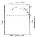
- the surface conduction electron-emitting devices exhibit an emission current Ie/device drive voltage Vf characteristic, and a device current If/device drive voltage Vf characteristic, as shown in FIG. 4 .
- the emission current Ie is much smaller than the device current If, and since it is difficult to show these currents in a diagram using the same scales, they are shown in two graphs using respectively different scales.
- the emission current Ie in the surface conduction electron-emitting devices exhibit the following three characteristics.
- the surface conduction electron-emitting device is a non-linear device having a clear threshold voltage Vth with respect to the emission current Ie.
- the emission current Ie varies depending upon the voltage Vf that is applied to the devices, it is possible to control the amount of the emission current Ie by making the voltage Vf variable.
- the surface conduction electron-emitting devices are also cold cathode devices, they have quick responsiveness which enables the emission time of the emission current Ie to be controlled by controlling the time when the voltage Vf is applied.
- the surface conduction electron-emitting devices can be used for the display apparatus in a favorable fashion.
- a voltage which is equal to or greater than the threshold voltage Vth is applied as appropriate to the devices being driven, and a voltage below the threshold voltage Vth is applied to the devices which are in a non-selected state.
- the amplitude of the voltage Vf applied to the devices is controlled to thereby enable the luminous brightness of the phosphors to be controlled, thus enabling image displays at various brightness.
- the illumination time of the phosphors can be controlled with the time that the voltage Vf is applied to the devices, whereby image displays of various brightness can be performed.
- modulation was performed on the quantity of the electron beam of the display panel by using the above-mentioned third characteristic.
- FIG. 5 shows one example of voltage applied to voltage supply terminals of the scanning wiring and the modulation wiring on the occasion of driving the display panel.
- the selection electric potential Vs is set to ⁇ 5V which is about 30% to 50% of a V SEL (see, FIG. 4 ), and the non-selection electric potential Vns is set to a ground electric potential (GND).
- the voltage V SEL is assumed to be a rated voltage for driving the surface conduction electron-emitting device of the embodiment.
- a pulse-width modulation signal of voltage amplitude Vpwm is supplied.
- pulse width of the pulse-width modulation signal to be supplied to the j-th modulation wiring was determined according to a value of the image data at the pixel in the row i at a column j of the image to be displayed, and pulse-width modulation signals corresponding to the value of the image data at respective pixels were supplied to all of the modulation wirings.
- the pulse width of the pulse-width modulation signal to be supplied to the j-th modulation wiring in compliance with the value of the image data of the pixel in the row i at the column j of the image to be displayed and its compensation amount, the lower luminance due to the influence of the voltage drop is compensated.
- voltage of the voltage Vpwm is set to +0.5 V SEL .
- the surface conduction electron-emitting device emits electrons when the voltage V SEL is applied to both end of the device as shown in FIG. 4 , but does not emit electrons at all in case of the applied voltage which is smaller than the voltage Vth. Also, the voltage Vth, as shown in FIG. 4 , is characterized to be larger than 0.5 V SEL .
- a basic problem to be solved is that, in particular, due to the voltage drop in the scanning wiring, the electric potential on the scanning wiring is increased, and thereby, the voltage to be applied to the surface conduction electron-emitting device is reduced, and the emission current from the surface conduction electron-emitting device is reduced.
- a device current for 1 device of the surface conduction electron-emitting device is around several 100 ⁇ A in case that the voltage V SEL was applied thereto.
- the device current flowing into the selected scanning wiring from the modulation wiring is simply a current for 1 pixel (i.e., the above-described several 100 ⁇ A). In this case, there is almost no case that the voltage drop occurs and light emission luminance is going down.
- the drive voltage applied to the both ends of the surface conduction electron-emitting device drops.
- the emission current for emitting light from the surface conduction electron-emitting device is going down and as a result, the light emission luminance was reduced.
- this phenomenon is not limited to cross patterns, but also occurs in some cases when displaying, for example, a window pattern or a natural image.
- FIG. 5 shows pulse-width modulation signals having pulse widths corresponding to the value of the inputted image data, and having their rising edges synchronized with each other.
- pulse-width modulation signals are outputted to each column, differences will occur depending on the inputted image data, but, generally speaking, in one horizontal scanning period, the number of illuminated pixels is greatest immediately after the rising of the pulse. After the rising edge, the pixels go out in sequence starting with the least bright pixels. Accordingly, the number of illuminated pixels during one horizontal scanning period decreases as time passes. Therefore, the amount of the voltage drop occurring in the scanning wiring also has a tendency to be greatest at the start of one horizontal scanning period, and then gradually diminish.
- the output of the pulse-width modulation signals changes with each unit of time that corresponds to a single gradation in the modulation. Therefore, the chronological change in the voltage drops also occurs with each unit of time corresponding to a single gradation of the pulse width modulation signal.
- the display panel of the display apparatus has several thousand modulation wirings, and it is very difficult to calculate the voltage drops at points where all of the modulation wirings intersect with the selected scanning wiring, and it is not realistic to manufacture hardware to calculate these in real time.
- the amount of voltage drop occurring on the scanning wiring is a specially continuous on the scanning wiring and a very smooth curve.
- the amount of the voltage drop differs also depending upon the display image, and also varies with respect to each time corresponding to 1 gradation of the pulse-width modulation, but overall, the amount of the voltage drop is larger near the raising edge of the pulse, and getting smaller or maintained as time passes. That is, there is no case that the size of the voltage drop increases during 1 horizontal scanning period when the drive method as shown in FIG. 5 is used.
- the calculation is carried out in a approximate simplified manner by use of a degeneracy model in which several thousand modulation wirings are concentrated into several to several tens of wirings to carry out calculation (This will be described in detail in the following calculation of the voltage drop by use of the degeneracy model.).
- FIG. 7A is a diagram for explaining blocks and nodes used when performing degeneration. In order to abbreviate the diagram, only the selected scanning wiring, the modulation wirings and the surface conduction electron-emitting devices connected to their intersecting portions are shown in FIGS. 7A to 7C .
- the diagram shows a point of time during one horizontal scanning period, and it is assumed that the illumination state of each pixel on the selected scanning wiring (i.e., whether the output from the modulation means is “H” or “L”) has already been determined.
- n modulation wirings a portion where the selected scanning wiring intersects with the n modulation wirings and the surface conduction electron-emitting device arranged at the intersection, are assumed to constitute one group that is defined as 1 block.
- the blocks are divided into 4 blocks.
- a position referred to as a “node” is established at the boundary positions of each block.
- the “node” refers to a horizontal position (reference point) for discretely calculating the amount of the voltage drop that will occur in the scanning wiring in the degeneracy model.
- 5 nodes from a node 0 to a node 4 are established at the boundary positions of the blocks.
- FIG. 7B is a diagram for explaining the degeneracy model.
- n modulation wirings included in 1 block in FIG. 7A are degenerated to 1 modulation wiring and this single degenerated modulation wiring is connected such that it is located in the center of the block on the scanning wiring.
- electric current sources are connected to the modulation wirings of each of the blocks which have been degenerated, and it is assumed that electric current total sums IF 0 to IF 3 in each of the blocks are flowing from the power sources.
- the potential at both ends of the scanning wiring is Vs in FIG. 7A , but it is the ground potential in FIG. 7B . It is because, according to the degeneracy model, the electric current flowing from the modulation wiring to the selected scanning wiring is modeled according to the above-mentioned electric current source, whereby the voltage drop amount at each portion on the scanning wiring can be calculated by treating the electricity supply portion as a reference (ground) potential to calculate the voltages at each part.
- the reason why the surface conduction electron-emitting device is abbreviated is because from the perspective of the selected scanning wiring if an equivalent electric current flows in from the column wirings, the generated voltage drop itself will not change at all due to whether or not the surface conduction electron-emitting devices are provided. Therefore, the electric current value that flows in from electric current source of each block is set to the total electric current value (Equation 1) of the device currents in each block, whereby the surface conduction electron-emitting device can be abbreviated.
- the wiring resistance in the scanning wirings in each block is n-times the wiring resistance r of the scanning wiring in one section.
- a “section” refers an area from the intersection between the scanning wiring and a certain column wiring to the intersection with the next column wiring.
- the wiring resistances of the scanning wirings in one section are assumed to be equal to each other.
- the “aij” refers to the voltage generated at the i-th node when the unit potential is applied only to j-th block. (Hereinafter, the foregoing will serve as the definition of “aij”.)
- the above-mentioned aij can be derived in a simple fashion according to Kirchhoff's Law as follows.
- Counti is a variable that will take a value of “1” when the “i”-th pixel on the selected scanning wiring is in the illuminated state, and will take a value of “0” when the pixel is in the turned-off state.
- the device current proportionate to the number of pixels illuminated within a given block flows from column wirings of each block to the selected scanning wiring.
- Device current IF of one device which is multiplied by the coefficient ⁇ is set as the device current IFS of one device considering that the voltage in the scanning wiring increases due the voltage drop, thus reducing the amount of the device current.
- FIG. 7C shows one example of calculation results of the voltage drop amounts DV 0 to DV 4 at respective nodes in a certain illuminated state by use of the degeneracy model.
- the voltage drop amount in a given illuminated state can be calculated in a simple fashion by using the degeneracy model.
- the voltage drop that will occur on the selected scanning wiring changes chronologically within one horizontal scanning period.
- these changes are predicted by obtaining the illuminated states of several points of time within one horizontal scanning period, and using the degeneracy model to calculate the voltage drops exhibited in those illuminated states. Note that, the number of illuminations within each block at a given point of time within one horizontal scanning period can be obtained in a simple fashion by referencing the image data at each block.
- the pulse width modulation circuit outputs a linear pulse width with respect to the value of the input data.
- the input data value is 0, the output is “L”; when the input data value is 255, “H” is outputted during one horizontal scanning period; and when the input data is 128, “H” is outputted for the first half of one horizontal scanning period, and “L” is outputted for the last half thereof.
- the number of illuminations at the time when the pulse-width modulation signal is started can easily be detected by performing counting on the input data to the pulse-width modulation circuit are greater than 0.
- the number of illuminations at the central point of time in one horizontal scanning period can be detected easily by counting the number of input data to the pulse width modulation circuit that are greater than 128.
- the number of illuminations in an arbitrary period of time can be counted easily by counting the number of outputs from the comparator that are positive.
- a time slot an amount of time referred to as a time slot
- the pulse width modulation uses the rising-edge time as a reference, and the pulse width after that point of time is modulated.
- the falling-edge time of pulse is used as the reference to modulate the pulse width
- the direction in which the time axis moves and the direction in which the time slot progresses will be opposite directions, but it goes without saying that the present invention may be applied nevertheless.
- the degeneracy model is used to repeatedly perform calculations to approximately and discretely calculate the chronological changes exhibited by the voltage drops within one horizontal scanning period.
- FIG. 8 illustrates an example in which the voltage drops are repeatedly calculated with respect to given,image data to calculate the chronological changes of the voltage drops in the scanning wiring.
- the voltage drops and their chronological changes shown here are one example given with respect to given image data, and it is natural that the voltage drops with respect to different image data will exhibit different changes.
- the degeneracy model is applied for calculation with respect to 4 points of time at which time slot is 0, 64, 128 and 192, respectively, and the voltage drop at each of those times is discretely calculated.
- the voltage drop amounts at each node are connected by a dotted line.
- the dotted line is drawn only to make the diagram easier to look at.
- the voltage drops calculated using the present degeneracy model are each calculated discretely at each of the node positions which are indicated by the white squares, the white circles, the black circles and the white triangles.
- FIG. 9 is a graph estimating the emission current that is emitted from a given surface conduction electron-emitting device in the illuminated state when the voltage drop shown in FIG. 8 occurs in the selected scanning wiring.
- the vertical axis indicates the emission current amount as percentages at each time and at each location where the degree of the emission current that is emitted when there is not voltage drop is 100%.
- the horizontal axis indicates the horizontal positions.
- the emission current Ie shown in FIG. 9 is calculated from the graphs showing the voltage drop amounts in FIG. 8 and the “drive voltage/emission current” shown in FIG. 4 . Specifically, the value of the emission current produced when the voltage calculated by subtracting the voltage drop amount from the voltage V DRV is applied, is simply plotted out mechanically.
- FIG. 8 primarily indicates the electric current that is emitted from the surface conduction electron-emitting device when it is in the illuminated state.
- the surface conduction electron-emitting devices in the turned-off state do not emit electric currents.
- FIGS. 10A , 10 B and 10 C are diagrams for explaining a method for calculating the voltage drop amount compensation data based on the changes with a time in the emission current. These diagrams illustrate an example of calculating compensation data for compensating an image data having an inputted data size of 64.
- the luminous amount of the luminance is equal to the emission charge amount in which the emission current from the emission current pulse is integrated with a time. Therefore, when fluctuation in the luminance caused by the voltage drop is considered hereinafter, explanations will be made based on the emission charge amount.
- the emission current is “IE”. Further, if the amount of time corresponding to 1 gradation in the pulse width modulation is assumed to be ⁇ t, then the emission charge amount Q 0 which should be emitted by the emission current pulse when the image data value is 64 is expressed as follows.
- the emission current pulse's amplitude IE times the pulse width (i e., 64 ⁇ t), which can be expressed as: Q 0 IE ⁇ 64 ⁇ t (Equation 6)
- the voltage drop in the scanning wiring causes the electric current amount that is emitted from the device to drop.
- the amount of the emission charge amount produced by the emission current pulse can be approximately calculated in a way which takes the influence of the voltage drop into consideration: i.e., the emission currents of the time slots 0 and 64 at node 2 are established as Ie 0 and Ie 1 , respectively, and if the emission current from 0 to 64 is approximated as a value changing in a linear fashion between Ie 0 and Ie 1 , then the emission charge amount Q 1 during this period will exhibit a trapezoidal area shown in FIG. 10B .
- the influence from the voltage drop can be removed by extending the pulse width by an amount equal to DC 1 .
- the compensation for the voltage drop is made and the pulse width is extended, it is considered that the emission current amounts at each of the time slots will change.
- the emission current is Ie 0
- the time slot (64+DC 1 )
- the emission current is Ie 1 .
- the emission current between the time slot 0 and the time slot (64+DC 1 ) is approximated as a value along a straight line connecting the emission currents at these 2 points.
- DC 1 ((2 ⁇ IE ⁇ Ie 0 ⁇ Ie 1 )/( Ie 0 + Ie 1 )) ⁇ 64 (Equation 9)
- the compensation data when the size of the image data is 64 is calculated as described above.
- the compensation amount CData may be added until DC 1 as described in the (Equation 9).
- FIGS. 11A to 11C are examples of calculation of the compensation data for image data having a value of 128, based on the calculated voltage drop amount.
- the voltage drop compensation amount was calculated as follows.
- the interval corresponding to the time slots 0 to 64 is defined as an interval 1
- the interval corresponding to the time slots 64 to 128 is defined as an interval 2 .
- the interval 1 portion is extended by an amount equivalent to DC 1 , thus being extended to an interval 1 ′
- the interval 2 part is extended by an amount equivalent to DC 2 , thus being extended to an interval 2 ′.
- the emission charge amount becomes the same as Q 0 described above.
- the emission currents at the beginning and end of each interval are altered by performing the compensation. However, in order to simplify the calculations, it is assumed that these emission currents do not change. In other words, the emission current at the beginning of the interval 1 ′ is Ie 0 , and the emission current at the end of the interval 1 ′ is Ie 1 . The emission current at the beginning of the interval 2 ′ is Ie 1 , and the emission current at the end of the interval 2 ′ is Ie 2 .
- DC 1 can be calculated in a fashion similar to (Equation 9).
- FIGS. 12A to 12C are examples of calculating compensation data for image data having a value of 192, based on the calculated voltage drop amount.
- the emission charge amount produced by the actual emission current pulse having received the influence by the voltage drop can be approximately calculated as follows. Namely, during the time slots 0, 64, 128 and 192 for node 2 , the emission current amounts at each of these time slots is Ie 0 , Ie 1 , Ie 2 and Ie 3 , respectively.
- an emission charge amount Q 6 during a period from the time slot 0 to 192 will be as represented by the 3 trapezoidal areas in FIG. 12C .
- the interval corresponding to the time slot 0 to 64 is defined as an interval 1
- the interval corresponding to the time slot 64 to 128 is defined as an interval 2
- the interval corresponding to the time slot 128 to 192 is defined as an interval 3 .
- the interval 1 part is extended by an amount equivalent to DC 1 , thus being extended to an interval 1 ′
- the interval 2 part is extended by an amount equivalent to DC 2 , thus being extended to an interval 2 ′
- the interval 3 part is extended by an amount equivalent to DC 3 , thus being extended to an interval 3 ′.
- the emission current amount becomes the same as Q 0 described above.
- the emission currents at the beginning and the end of each interval remain unchanged before and after the compensation. That is, the emission current at the beginning of the interval 1 ′ is Ie 0 , and the emission current at the end of the interval 1 ′ is Ie 1 .
- the emission current at the beginning of the interval 2 ′ is Ie 1
- the emission current at the end of the interval 2 ′ is Ie 2 .
- the emission current at the beginning of the interval 3 ′ is Ie 2
- the emission current at the end of the interval 3 ′ is Ie 3 .
- DC 1 and DC 2 can each be calculated in the same ways as shown in (Equation 9) and (Equation 12).
- DC 3 ((2 ⁇ IE ⁇ Ie 2 ⁇ Ie 3 )/( Ie 2 + Ie 3 )) ⁇ 64 (Equation 15)
- the compensation data is 0, and the compensation data CData to be added to the image data is also 0.
- the reason why the compensation data is calculated in this scattered fashion for image data 0, 64, 128 and 192 is to reduce the volume of the calculations. In other words, if the same calculation were to be performed on all the image data, the volume of the calculations would become extremely large, and the amount of hardware for performing the calculations would become extremely great. On the other hand, there is a tendency that the greater the image data at a given node position, the greater the compensation data will be. Therefore, when the compensation data for an arbitrary image data is to be calculated, the calculation volume can be significantly decreased by using a linear approximation to interpolate between points in the vicinity of the image data for which the compensation data has already been calculated. Note that the interpolation will be explained in detail when discrete compensated data interpolating means is explained.
- the compensation data for the 0, 64, 128 and 192 image data at all the node positions can be calculated.
- the calculation was carried out at only the 4 points of the time slots 0, 64, 128, and 192, but in case that the calculation was carried out at intervals of 16 time slots among the time slots 0 to 255 (i.e., the reference values of the image data are set every 16 in the value of the image data), more preferable result was obtained.
- FIG. 13A An example, obtained by this method, of discrete compensation data to certain input image data is shown in FIG. 13A .
- a horizontal axis corresponds to the horizontal display position, and positions of respective nodes are described.
- a vertical axis corresponds to the value of the compensation data.
- the compensation data calculated discretely is discrete one to positions of respective nodes, and is not one providing compensation data in an arbitrary horizontal position (column wiring number). Also, at the same time to it, it is compensation data to the image data having the size of the reference values of several predetermined image data at respective node positions, but is not one providing compensation data in accordance with size of actual image data value.
- compensation data fit in with the size of the input image data value in respective column wirings is calculated by interpolating the compensation data calculated discretely.
- FIG. 13B is a diagram showing a method for calculating compensation data corresponding to image data “Data” at a position x located between a node n and a node n+1.
- the compensation data has already been discretely calculated for positions Xn and Xn+1 at the node n and at the node n+1. Further, the inputted image data Data has a value between image data reference values Dk and Dk+1 for which discrete compensation data have already been calculated.
- the compensation data CA for the pulse width Dk at the position x can be calculated in the following way according to the linear approximation using the values of CData[k] [n] and CData[k] [n+1].
- CA ( Xn + 1 - x ) ⁇ CData ⁇ [ k ] ⁇ [ n ] + ( x - X n ) ⁇ CData ⁇ [ k ] ⁇ [ n + 1 ] X n + 1 - X n ( Equation ⁇ ⁇ 17 )
- the compensation data CD for the image data Data at the position x can be calculated as follows.
- CD CA ⁇ ( D k + 1 - Data ) + CB ⁇ ( Data - D k ) D k + 1 - D k ( Equation ⁇ ⁇ 19 )
- the compensation data calculated herewith is added to the image data to compensate the image data and the pulse-width modulation is carried out in compliance with the image data after the compensation, and thereby, deterioration of the image quality due to the voltage drop can be reduced and the image quality can be improved.
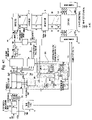
- FIG. 14 is a block diagram showing an outline of its circuit structure.
- 1 designates the display panel of FIG. 2
- Dx 1 to DxM and Dx 1 ′ to DxM′ designate voltage supply terminals for the scanning wirings of the display panel
- Dy 1 to DyN designate voltage supply terminals for the modulation wirings of the display panel
- Hv designates a high-voltage supply terminal for applying acceleration voltage between a face plate and a rear plate
- Va designates a high-voltage power supply
- 2 designates a scanning circuit (scanning unit)
- 3 designates a synchronization signal separation circuit
- 4 designates a timing generation circuit
- 7 designates a RGB conversion part for converting YPbPr signals separated by the synchronizing signal separation circuit 3 into RGB signals
- 17 designates an inverse ⁇ processing part
- 5 designates a shift register for 1 line of the image data
- 6 designates a latch circuit for 1 line of the image data
- 8 designates a pulse-width modul
- R, G, and B designate parallel input image data
- Ra, Ga, and Ba designate RGB-parallel image data to which inverse y conversion processing described later is applied
- Data is image data which was parallel/serial-converted by a data array conversion part 9
- CD designates compensation data which was calculated by the compensation data calculation unit 14
- Dout designates image data which was compensated(compensated image data) by adding the compensation data to the image data by the adder 12 .
- the display apparatus of this embodiment can display NTSC, PAL, SECAM, HDTV and other such television signals, and also computer outputs such as VGA and the like.
- synchronization signals Vsync, Hsync are separated by a synchronization signal separation circuit 3 , and supplied to a timing generation circuit 4 .
- the image signal from which the synchronization signals were separated are supplied to a RGB conversion part 7 .
- a conversion circuit from YPbPr to RGB not-shown low pass filter and A/D converter etc. are disposed inside of the RGB conversion part 7 .
- the RGB conversion part 7 converts YPbPr which is filtered with the low pass filter to digital RGB signals by the A/D converter, and supplies the same to the inverse ⁇ processing part 17 .
- the timing generation circuit 4 has a built-in PLL circuit, and it generates timing signals synchronized to synchronization signals from various image sources and generates operation timing signals for each part.
- timing signals generated by the timing generation circuit 4 include a TSFT for controlling operating timing of the shift resistor 5 ; a control signal Dataload for latching data from the shift resistor 5 to the latch circuit 6 ; a pulse width modulation start signal Pwmstart for the modulation circuit 8 ; a clock Pwmclk for the pulse width modulation; and a timing signal Tscan for controlling the operation of the scanning circuit 2 .
- the scanning circuits 2 and 2 ′ in FIG. 14 are circuits for outputting the selection electric potential Vs or the non-selection electric potential Vns to the connection terminals Dx 1 to DxM to sequentially scan the display panel 1 in steps of 1 line during 1 horizontal scanning period.
- the scanning circuit 2 and 2 ′ has a variable power supply for setting the selection electric potential Vs on the basis of a selection electric potential instruction value SVs which is supplied from a drive voltage calculation part to be described later.
- Vs the selection electric potential
- the scanning circuits 2 and 2 ′ are circuits which sequentially change the scanning wiring that is being selected with respect to each horizontal period, in synchronous with a timing signal Tscan from the timing generation circuit 4 to carry out the scanning.
- Tscan designates a group of timing signals generated of vertical synchronization signals and horizontal synchronization signals etc.
- the scanning circuits 2 and 2 ′ are composed of M number of switches and shift registers etc. It is desirable that these switches are composed of transistors and FETs.
- the scanning circuits are connected to both ends of the scanning wiring of the display panel to drive from the both ends.
- the method in this embodiment is applicable to a case that the scanning circuits are not connected to the both ends of the scanning wiring. In that case, the above-described (Equation 3) may be modified.
- a panel drive power supply which provides the selection electric potential Vs and the non-selection electric potential Vns is disposed in the scanning circuits, but it is desirable that such panel drive power supply is formed as an independent power supply circuit separated from the scanning circuits.
- CRTs have a luminous characteristic of the approximately 2.2 power to their inputs (hereinafter referred to as inverse ⁇ characteristic).
- Input image signals are converted generally in compliance with the ⁇ characteristic of the 0.45 power to realize a linear luminous characteristic on the occasion of displaying on CRT.
- the display panel 1 of the display apparatus in this embodiment in case that the modulation is carried out by adjusting duration of time that the drive voltage is applied, has a substantially linear luminous characteristic with respect to length of time that the drive voltage is applied. Accordingly, the input image signal may be converted on the basis of the inverse ⁇ characteristic (hereinafter, referred to as inverse ⁇ conversion).
- FIG. 16 shows the detail of a inverse ⁇ processing part 17 .
- This inverse ⁇ processing part 17 is a block for carrying out the inverse ⁇ conversion of the input image signal.
- the inverse ⁇ processing part 17 in this embodiment realizes the inverse ⁇ conversion processing by use of a memory.
- the number of bits of the image signals R, G, and B are set to 8 bits, and the number of bits of the image signals Ra, Ga, and Ba as outputs from the inverse ⁇ processing part 17 are also set to 8 bits, and the inverse ⁇ processing part 17 is configured by using a memory having 8 bit addresses and 8 bit data with respect to each color.
- a data array conversion part 9 in FIG. 14 is a circuit for performing a parallel/serial conversion on the RGB parallel image signals Rb, Gb and Bb, to make them appropriate for pixel array of the display panel.
- the data array conversion part 9 is composed of FIFO (a First In First Out) memories 2021 R, 2021 G and 2021 B for each of the RGB colors, and a selector 2022 .
- the FIFO memory has two memories capable of holding number of words equal to the number of horizontal pixels, where one of the memories is for odd-number lines, and the other memory is for even-number lines.
- image data from an odd-number line is inputted, this data is inputted into the FIFO for the odd-number line while image data stored in the immediately previous horizontal scanning period is read out from the FIFO memory for the even-number line.
- image data from the even-number line is inputted, the data is written into FIFO for the even-number line while the image data stored in the immediately previous horizontal scanning period is read out from the FIFO for the odd-number line.
- the data read out from the FIFO memory undergoes the parallel/serial conversion by the selector in accordance with the pixel array of the display panel, and is then outputted as serial image data SData for the RGB.
- the data array conversion part 9 operates based on the timing control signals from the timing generation circuit 4 .
- the adder 12 in FIG. 14 is a unit for adding the compensation data CD from the compensation data calculation unit 14 and the image data Data. By carrying out the addition, the image data Data is compensated and is, as image data Dout, transferred to the shift register 5 .
- the maximum value of the compensation data to be added is estimated in advance, and, in order to prevent the overflow from occurring when its maximum value was added, a range of a value that the image data can take may be lessen in advance.
- the input image data may be limited on the occasion of carrying out A/D conversion, and a multiplier may be provided so that a gain of more than 0 and less than 1 is multiplied with the input image data to limit its range.
- the image data SData which has been reordered by the data array conversion part 9 is inputted into the compensation data calculation unit 14 and into the delay circuit 19 .
- a compensation data interpolating part of the compensation data calculation unit 14 described below cross-references horizontal position information x from the timing control circuit and the value of the image data SData to calculate the compensation data CD which will be suitable for each horizontal position and for each image data value.
- the delay circuit 19 is provided to absorb the time required for the calculation of the compensation data.
- the delay circuit 19 performs the delay so that the compensation data corresponding to the image data is added accurately.
- the delay circuit 19 is constituted by using a flip-flop circuit.
- the image data Dout as outputs from the adder 12 undergoes the serial/parallel conversion by the shift resistor 5 , whereby the image data Dout changes from its serial data format into parallel image data ID 1 to IDN per modulation wiring and then it is outputted to the latch circuit 6 .
- the latch circuit 6 latches the data from the shift resistor 5 immediately before one horizontal interval is started, based on the timing signal Dataload.
- the outputs from the latch circuit 6 are delivered to the modulation unit 8 as parallel image data D 1 to DN.
- the image data ID 1 to IDN and D 1 to DN are each composed of 8 bits. Their operation timing is based on the timing control signals TSFT and Dataload from the timing generation circuit 4 .
- the parallel image data D 1 to DN outputted from the latch circuit 6 is provided to the modulation unit 8 .
- the modulation unit 8 is a pulse width modulation circuit (PWM circuit) including a PWM counter, and a comparator and a switch (a FET in FIG. 18A ) for each modulation wiring.
- PWM circuit pulse width modulation circuit
- the relationship between the image data D 1 to DN and the output pulse width from the modulation unit 8 is a linear relationship.
- FIG. 18C shows 3 examples of an output waveform from the modulation unit 8 .
- the waveform depicted at the top is a waveform when the input data to the modulation unit 8 is 0.
- the waveform depicted in the middle is a waveform when the input data to the modulation unit 8 is 256.
- the waveform depicted on the bottom is the waveform when the input data to the modulation unit 8 is 511.
- the number of bits of the input data D 1 to DN to the modulation unit 8 is, as described above, on the ground that the overflow does not occur, set to 9 bits (in addition, in the above-stated description, there are places describing that, when the input data of the modulation unit 8 is 511, the modulation signal of pulse width corresponding to 1 horizontal scanning period is outputted, but in detail, as shown in FIG. 18C , although it is very short time, no-drive periods are disposed at points of before a pulse is going up and after the pulse went down so that flexibility of timing is provided.).
- FIG. 19 is a timing chart showing the operation of the modulation unit 8 according to the present invention.
- Hsync denotes a horizontal synchronization signal
- Dataload denotes a load signal provided to the latch circuit 6
- D 1 to DN denote the input signals to columns 1 to N of the modulation unit 8 described above
- Pwmstart denotes a synchronization clear signal for the PWM counter
- Pwmclk denotes a clock of the PWM counter.
- XD 1 to XDN represent outputs of the modulation unit 8 pertaining to columns 1 to N.
- the latch circuit 6 latches the image data and transfers the data to the modulation unit 8 .
- the PWM counter starts the count based on the Pwmstart and the Pwmclk, and when the count value reaches 511, it stops the counter and holds the value 511.
- the comparator provided to each of the columns compares the counter value of the PWM counter and the image data from each of the columns. When the value of the PWM counter is greater than the image data, it outputs “High”, and it outputs “Low” during all the other periods.
- the comparator output is connected to the gate of the switch at each column. While the comparator output is “Low”, the switch on a VPWM side shown in FIG. 18A is turned “ON”, and the switch on a GND side is turned “OFF”, so that the modulation wiring connects to the voltage VPWM. In contrast, while the comparator output is “High”, the switch on the VPWM side in FIG. 18A is turned “OFF”, and the switch on the GND side is turned “ON”, so that the voltage in the modulation wirings connects with the ground potential.
- each part operates as described above, whereby the pulse-width modulation signal outputted by the modulation unit 8 exhibits the waveform with the synchronized rising edge of the pulse as shown in D 1 , D 2 and DN in FIG. 19 .
- the average luminance level detection unit 221 for detecting the luminance information is a unit for detecting the average luminance with respect to each frame in reference to the image data Ra, Ga, and Ba after the inverse ⁇ conversion. This unit calculates summation of the image data in frame, by adding the image data of Ra, Ga, and Ba with respect to each frame, and detects the average luminance level by dividing the final total of the image data in frame by the number of pixels of the screen.
- the detection of the luminance information which is used in this invention is not limited to this method but other units as described above may be used, if it can detect a value corresponding to the average luminance level.
- a value corresponding to the average luminance level may be gotten by dividing the total sum of the image data by one of some adequate fixed values instead of dividing by the number of pixels of the screen. In this case, if the value is set to the n-th power of 2, division can be realized by a bit sift to simplify the structure of hardware.
- the meaning of the average luminance level is almost same to that of APL (Average Picture Level).
- the drive voltage calculation part 222 is a drive voltage calculation unit which calculates a drive voltage instruction value, on the basis of the average luminance calculated in the average luminance level detection unit 221 .
- the calculated drive voltage instruction value SV DRV is, as shown in FIG. 14 , supplied to a compensation data calculation unit 14 described later and, as a selection electric potential instruction value SVS which is found by subtracting the modulation electric potential from the drive voltage, supplied to the scanning circuits 2 and 2 ′.
- a table ROM is used on the occasion of calculating the instruction value SV DRV for the drive voltage V DRV from the average luminance ( FIG. 20A ). That is, it was configured such that, when the average luminance is inputted as an input (address terminal) of the table ROM, the instruction value SV DRV of the drive voltage to be set is outputted from an output (data terminal) of ROM.
- FIG. 20B content which was stored in the table ROM in this embodiment is shown in FIG. 20B .
- a horizontal axis is set for the average luminance and, in order to make the figure clearly understandable, it is normalized by setting the average luminance to 1 when the input image signal of 1 frame is of an all-white screen.
- a vertical axis of the same figure is not the drive voltage instruction value SV DRV but the actual drive voltage V DRV .
- V SEL is rated drive voltage of the surface conduction electron-emitting device in this embodiment.
- the compensation data calculation circuit 14 is a circuit which calculates the compensation data of the voltage drop corresponding to the drive voltage of the display panel 1 , by the above-described compensation data calculation method.
- the compensation data calculation unit 14 is, as shown in FIG. 21 , composed of two blocks of a discrete compensation data calculation part and a compensation data interpolation part.
- the discrete compensation data calculation part makes reference to the drive voltage instruction value SV DRV which is outputted from the drive voltage calculation part 222 , and calculates the voltage drop amount in compliance with the inputted image signal from the same signal, and calculated the compensation data discretely from the voltage drop amount.
- This part in order to reduce calculated amount and hardware amount, adopts the concept of the above-described degeneracy model, and calculates the compensation data discretely.
- the drive voltage instruction value SV DRV which is a value corresponding to the drive voltage V DRV
- the device current amount which is used for the calculation is renewed and the voltage drop amount is calculated.
- the compensation data calculated discretely is interpolated by the compensation data interpolation part (compensation data interpolation unit), and the compensation data CD fit in with the value of the image data and its horizontal display position x is calculated.
- FIG. 22 shows the discrete compensation data calculation part for calculating the compensation data discretely.
- the discrete compensation data calculation part is a unit which realizes a function as the voltage drop amount calculation part for dividing the image data into blocks to calculate a statistical amount (the number of lighting) with respect to each block, and calculating the time change of the voltage drop amount at respective node positions from the statistical amount, a function for converting the voltage drop amount with respect to each time into the light-emission luminance amount, a function for integrating the light-emission luminance amount in a time direction to calculate a total light-emission luminance amount, and a function for calculating the compensation data to the reference value of the image data at discrete reference points.
- 100 a to 100 d designate a lighting number counting unit
- 101 a to 101 d designate register groups for storing the number of lighting in respective times with respect to each block
- 102 designates CPU
- 103 designates a table memory (voltage drop amount storage unit) for storing the parameter aij described in (Equation 2) and (Equation 3)
- 113 designates a register for storing the drive voltage instruction value SV DRV which was supplied from the drive voltage calculation part
- 112 designates a table memory for calculating the device current amount for calculating the voltage drop amount from the drive voltage instruction value SV DRV
- 104 designates a temporary register for temporarily storing calculation results
- 105 designates a program memory in which programs for the CPU are stored
- 111 designates a table memory in which conversion data for converting the voltage drop amounts into emission current amounts is stored
- 106 designates a register group for storing calculation results of the above-described discrete compensation data.
- the lighting number counting units 100 a to 100 d are composed of comparators and adders etc. as described in FIG. 22B .
- the image signals Ra, Ga, and Ba are inputted to comparators 107 a to 107 c , respectively, and are compared one after another with a value of Cval.
- Cval corresponds to the above-described reference value set to the image data.
- the comparators 107 a to 107 d compare Cval with the image data, and if the image data value is larger, High is outputted, and if smaller, Low is outputted.
- Outputs of the comparators 107 a to 107 c are added to one another by the adders 108 and 109 , and further, by the adder 110 , addition is carried out with respect to each block, and the addition results with respect to each block are stored in the resister groups 101 a to 101 d as the number of lighting with respect to each block.
- the lighting number counting unit 100 a counts the number of image data which is larger than 0 out of the image data, and stores a final total with respect to each block into the register 101 a .
- the lighting number counting unit 100 b counts the number of image data which is larger than 64 out of the image data, and stores a final total with respect to each block into the register 101 b .
- the lighting number counting unit 100 c counts the number of image data which is larger than 128 out of the image data, and stores a final total with respect to each block into the register 101 c.
- the CPU reads out the parameter table aij stored in the table memory 103 as needed, calculates the voltage drop amount in accordance with (Equation 2) to (Equation 5), and stores calculation results in the temporary register 104 .
- the CPU 102 firstly makes reference to contents of the register 113 , and stores the drive voltage instruction value SV DRV which was instructed by the drive voltage calculation part 21 .
- the CPU refers contents of the table memory 3 ( 112 ).
- a relation of a drive voltage vs. device current IF is stored, and when the drive voltage instruction value SV DRV is inputted to the table memory 3 , the device current IF corresponding to it is outputted.
- the device current amount IF found herewith in (Equation 5) calculation of the voltage drop amount is carrying out.
- the CPU 102 has a sum of products calculation function for carrying out a calculation of (Equation 2) smoothly.
- the CPU 102 does not have to carry out the sum of products calculation, and for example, its calculation results may be put into the memory. That is, the number of lighting of respective blocks is set as inputs, and with respect to conceivable all input patterns, the voltage drop amount at respective node positions can be stored in the memory.
- the CPU 102 reads out the voltage drop amount with respect to each time and each block from the temporary register 104 , and makes reference to the table memory 2 ( 111 ), and converts the voltage drop amount into the emission current amount, and calculates the discrete compensation data in accordance with (Equation 6) to (Equation 16).
- the calculated discrete compensation data is stored in the register group 106 .
- the compensation data interpolation part is a unit for calculating the compensation data fit in with a position where the image data is displayed (horizontal position), and the value of the image data. This unit, by interpolating the compensation data calculated discretely, calculates the compensation data in accordance with the display position (horizontal position) of the image data and the value of the image data.
- FIG. 23 is a diagram for explaining the compensation data interpolation part.
- 123 designates a decoder-a for determining node numbers n and n+1 of the discrete compensation data to be used for the interpolation from the display position (horizontal position) x of the image data
- 124 designates a decoder-b for determining k and k+1 in (Equation 17) to (Equation 19) from the size of the image data.
- selectors 125 to 128 are selectors for selecting the discrete compensation data and supplying it to the linear approximation unit.
- 120 to 122 designates the linear approximation units for carrying out the linear approximation for (Equation 17) to (Equation 19), respectively.
- FIG. 24 shows a structural example of the linear approximation unit 120 .
- the linear approximation unit as shown in an operator of (Equation 17) to (Equation 19), can be composed of a subtracter, a multiplier, an adder, a divider etc.
- the addition result of the adder may be shifted by an amount equivalent to a multiplier of the power, and there is no necessity to darlingly prepare the divider.
- FIG. 25 shows a timing chart of operational timing of the units.
- Hsync is the horizontal synchronization signal
- DotCLK is a clock made from the horizontal synchronization signal Hsync by a PLL circuit inside the timing generation circuit 4
- R, G, B are digital image data from an input switching circuit
- Data is image data which has already undergone data array conversion
- Dout is the compensated image data which has undergone the voltage drop compensation
- TSFT is the shift clock for sending the compensated image data Dout to the shift register 5
- Dataload is a load pulse for latching the data to the latch circuit 6
- Pwmstart is a start signal for the above-mentioned pulse width modulation
- a modulation signal XD 1 is one example of the pulse width modulation signal provided to the modulation wiring 1 .
- the digital image data RGB is forwarded from the input switching circuit.
- image data inputted at a horizontal scanning period I are indicated by R_I, G_I and B_I.
- the image data R_I, G_I and B_I are accumulated in the data array conversion part 9 during the one horizontal interval.
- the image data R_I, G_I and B_I are outputted as digital image data Data_I in correspondence with the arrangement of the pixels in the display panel 1 .
- the image data R_I, G_I and B_I is inputted into the compensation data calculation circuit 14 during the horizontal scanning period I.
- the compensation data calculation circuit 14 counts the number of illuminations as described above, and when it finishes counting it calculates the voltage drop amount. After the voltage drop amount is calculated, the discrete compensation data is calculated and the results of the calculation are stored in the register.
- the compensation data interpolation part interpolates from the discrete compensation data in synchronization with the image data Data_I before the one horizontal scanning period being outputted from the data array conversion part 9 , and thus the compensation data is calculated.
- the interpolated compensation data is immediatly converted by a gradation number conversion part (not shown), and then the result is provided to the adder 12 .
- the image data Data and the compensation data CD are added together one after the other, and then the compensated image data Dout is forwarded to the shift register 5 .
- the shift register 5 stores the compensated image data Dout for one horizontal interval in accordance with TSFT, and also performs the serial/parallel conversion and outputs the parallel image data ID 1 to IDN to the latch circuit 6 .
- the latch circuit 6 latches the parallel image data ID 1 to IDN from the shift register 5 in correspondence with the rising edge of the Dataload signal, and then transfers the latched image data D 1 to DN to the pulse width modulation unit 8 .
- the modulation unit 8 outputs the pulse-width modulation signal having a pulse-width which corresponds to the latched image data.
- the pulse width outputted by the modulation circuit 8 is, as a result, displayed after 2 horizontal scanning periods subsequent to the inputted image data.
- the voltage drop compensation circuit can carry out the compensation properly, which was very acceptable.
- the voltage drop compensation circuit which corresponded to the change of the drive voltage so as to reduce the power consumption was described, but even in case that the drive voltage is changed for another purpose, the voltage drop compensation can be carried out well as a matter of course.
- a mode for dynamically displaying by relatively increasing a peak luminance (dynamic mode) and a mode for displaying by emphasizing the power consumption and relatively decreasing the peak luminance (power consumption emphasis mode) etc. are prepared in advance, and set to be selectable based upon user's taste. Even in case that such a plurality of display modes are prepared, the mode is selected in accordance with a setting of a user and the drive voltage is controlled, and thereby, adjustment of the display image is carried out easily and the voltage drop compensation amount is adjusted corresponding to the adjusted drive voltage and good compensation can be carried out.
- the display apparatus is used as not only a television but also as a monitor for a computer, since a user uses the monitor by looking straight at it, it is desirable that it is used by suppressing the luminance as compared with a case that it is used as the television.
- the display is carried out such that the luminance is suppressed by adjusting the drive voltage, and the good voltage drop compensation can be carried out corresponding to the adjusted drive voltage.
- an identification of whether an image being displayed at present is an image of a computer or an image of a television may be carried out by detecting from which of an image supply terminal for a television and an image supply terminal for a computer, the image is supplied. Also, the identification may be carried out on the basis of an input setting of a user interface unit such as a remote controller by which the image supply terminal can be set, a detection result by an automatic detection unit, and a detection result of an external environment detection unit such as a photo-sensor etc.
- the selection electric potential of the scanning circuit was changed but, as described above, it is not limited to this.
- the discrete image data reference values are set and the reference points are set on the scanning wiring, and the compensation data at that reference point with regard to the image data value having size of the image data reference value was calculated discretely. Further, by interpolating the compensation data calculated discretely, the compensation data in accordance with the horizontal display position and the value of the input image data is calculated and added to the image data so that the compensation was realized.
- the compensation amount of the image data for compensating the voltage drop can be easily calculated, and it could be realized by very simple hardware.
- the voltage drop compensation could be carried out properly.
- the parameter change for changing the drive voltage instruction value was carried out, but it is possible to change the average luminance level of 1 frame image data by changing the coefficient which is multiplied with the output image data Dout. Such embodiment will be described later.
- a display apparatus has a emission charge amount compensation unit for compensating change of the emission charge amount due to influence of the voltage drop, and, in an display apparatus in which the emission charge amount compensation unit calculates the compensated image data by compensating the input image data so as to correspond to the emission charge amount to be emitted, and the modulation unit outputs pulse wave forms which are applied to the column wiring according to the calculated compensated image data, is characterized by having a current value calculation unit for calculating an average current value corresponding to the light-emission luminance of the display apparatus based upon the integrated value of the input image data as a luminance desired value.
- a compensated image data calculation unit which calculates the compensated image data as the image data in which influence of the voltage drop was compensated
- a modulation unit which receives the compensated image data as input and outputs a modulation signal to the column wiring
- a current value calculation unit which calculats an average current value corresponding to the light-emission luminance of the display apparatus based upon the integrated value of the input image data.
- the current value calculation unit has an integration unit which integrates the input image-data, and takes an output of the integration unit as the average current value corresponding to the light-emission luminance of the display apparatus.
- the current value calculation unit has an integration unit which integrates the input image data, and takes a result of multiplying an output of the integration unit with the coefficient as the average current value corresponding to the light-emission luminance of the display apparatus.
- an electric power limitation unit in which, the average current value calculated by the current calculation unit is compared with a predetermined reference current value, and in case that the average current value is larger than the reference current value, electric power relating to the light-emission luminance of the display apparatus is limited.
- the electric power limitation unit has a function in which, a coefficient for carrying out the power limitation is calculated from the reference current value and the average current value, and the coefficient for carrying out the power limitation is multiplied so as to adjust the amplitude of the compensated image data.
- the electric power limitation unit multiplies the coefficient G′ with the compensated image data, and calculates the compensated image data in which the amplitude was adjusted.
- the electric power limitation unit multiplies the coefficient G′ with the image data before the compensation is applied.
- the amplitude adjustment unit multiplies the coefficient G′′ with the compensated image data, and calculates the compensated image data in which the amplitude was adjusted.
- the amplitude adjustment unit multiplies the coefficient G′′ with the image data before the compensation is applied.
- the integration unit calculates the integrated value of the input image data in frame.
- the reference current value is a value which is determined in advance in accordance with the power consumption of the display apparatus.
- the reference current value is changeable by at least one unit out of the user interface unit and the external environment detection unit.
- the compensated image data calculation unit in consideration of the influence of the voltage drop, expands the size of the image data to be inputted to the compensated image data calculation unit to thereby calculate the compensated image data.
- the amplitude adjustment unit detects a maximum value of an output of the compensated image data calculation unit with respect to each frame, and, in order for the maximum value to be accommodated within an upper limit of the input range of the modulation circuit, calculates a coefficient for adjusting the amplitude of the compensated image data in an accommodative manner.
- the amplitude adjustment unit makes reference to outputs of a plurality of frames which are precedent to the current frame by the compensated image data calculation unit, and in order for those values to correspond to the input range of the modulation unit, calculates the coefficient for adjusting the amplitude of the compensated image data in an accommodative manner.
- the coefficient for adjusting the amplitude of the compensated image data is a coefficient which always has a constant value and was determined in advance.
- the coefficient for adjusting the amplitude of the compensated image data is a coefficient which was determined such that, in case that the value of the input image data is maximized, an output of the compensated image data calculation unit does not overflow above the input range of the modulation unit.
- the compensated image data calculation unit has a unit which predicts and calculates, in accordance with the input image data, spatial distribution and time change of the voltage drop amount which should occur on the row wiring during 1 horizontal scanning period, and a unit which calculates the compensated image data in which compensation is applied to the input image data, from the calculated voltage drop amount.
- the compensated image data calculation unit has a unit which discretely predicts and calculates, in accordance with the input image data, spatial distribution and time change of the voltage drop amount which should occur on the row wiring during 1 horizontal scanning period, and a unit which calculates the compensated image data in which compensation is applied to the input image data, from the calculated voltage drop amount.
- the compensated image data calculation unit has a unit which discretely predicts and calculates, in accordance with the input image data, spatial distribution and time change of the voltage drop amount which should occur on the row wiring during 1 horizontal scanning period, a discrete compensated image data calculation unit which discretely calculates the compensated image data to the image data corresponding to time when the voltage drop was calculated, in a spatial position where the voltage drop amount was calculated, from the calculated voltage drop amount, and a compensated image data interpolation unit which interpolates an output of the discrete compensated image data calculation unit and calculates the compensated image data corresponding to a value and a horizontal display position of the input image data.
- the compensated image data which is calculated by the compensated image data calculation unit is adjusted such that the emission charge amount of the compensated image data becomes the emission charge amount of the input image data in case that there is no voltage drop amount which should occur on the row wiring.
- the voltage drop compensation circuit in this embodiment predicts and calculates the deterioration of the display image which occurs due to the voltage drop in accordance with the input image data, and calculates the compensation data for compensating it, and applies the compensation to the input image data.
- FIG. 26 is a block diagram showing an outline of its circuit structure. With regard to the same portions as the functional blocks used in the structure shown in FIG. 14 , the same numerals are applied thereto, and their explanations will be omitted here.
- 23 designates a selector for switching an image signal of a television and an image signal of a computer
- 20 designates a maximum value detection circuit
- 21 designates a gain calculation unit.
- synchronization signals Vsync, Hsync are separated by a synchronization signal separation circuit 3 , and supplied to a timing generation circuit 4 .
- the image signal from which the synchronization signals were separated are supplied to a RGB conversion part 7 .
- a conversion circuit from YPbPr to RGB not-shown low pass filter and A/D converter etc. are disposed inside of the RGB conversion part 7 .
- the RGB conversion part 7 converts YPbPr to digital RGB signals, and supplies the same to a selector 23 .
- An image signal such as VGA which is outputted from a computer is A/D-converted by the not-shown A/D converter, and supplied to the selector 23 .
- the selector 23 based upon which image signal a user wish to display, switches the television signal and the computer signal accordingly, and outputs it.
- the scanning circuits 2 and 2 ′ are circuits which output the selection electric potential Vs or the non-selection electric potential Vns to the connection terminals Dx 1 to DxM, in order to sequentially scan the display panel in steps of 1 line during 1 horizontal scanning period.
- a different point from the scanning circuit 2 and 2 ′ shown in FIG. 15 is a point that the power supply Vs is a fixed power supply, and the selection electric potential Vs itself is a fixed value which was set in advance.
- a basic structure of the adder 12 is the same as in the first embodiment.
- the compensation is applied to the image data Data, which is transferred to the maximum value detection circuit 20 and the multiplier 22 as the compensated image data Dout.
- the number of bits of the compensated image data Dout as the output of the adder 12 is determined to prevent overflow from occurring on the occasion of adding the compensation data CD to the image data Data.
- the number of bits of the modulation unit 8 is 8 bits, and the number of bits of the compensated image data Dout as the output of the adder 12 is 10 bits.
- the compensated image data is connected to the input of the modulation unit 8 as it is, the overflow is to occur. Then, before inputted to the modulation unit 8 , it is necessary to adjust the amplitude of the compensated image data.
- this method is called as a fixed gain method.
- the overflow does not occur but, with regard to an image in which the average luminance is low, since, regardless of being capable of displaying with a larger gain, a small gain is multiplied, there is a case that the luminance of the display image becomes dark.
- the maximum value of the compensated image data may be detected with respect to each frame, and a gain in which this maximum value is accommodated in the input range of the modulation unit 8 may be calculated, and the gain may be multiplied with the compensated image data so that the overflow is prevented.
- this method is called as an adaptive type gain method.
- the adaptive type gain method it is necessary to provide a maximum value detection circuit 20 for detecting the maximum value MAX of the compensated image data Dout with respect to each frame, a gain calculation unit for calculating a gain G 1 to be multiplied with the compensated image data from the maximum value, and a multiplier for multiplying the compensated image data Dout with the gain G 1 , etc.
- the gain for preventing the overflow is calculated in frame. For example, it is possible to prevent the overflow by calculating the gain with respect to each 1 horizontal line but, in that case, since, due to a difference of the gain with respect to each 1 horizontal line, uncomfortable feeling is generated on the display image, it is not desirable.
- the maximum value detection circuit 20 is a unit for detecting a value which becomes the maximum in the compensated image data Dout of 1 frame portion.
- the same unit is a circuit which can be configured by a comparator and a register etc.
- the same unit is a circuit which compares a value stored in the register with the value of the compensated image data Dout which is sequentially transferred, and, in case that the value of the compensated image data Dout is larger than the value of the register, renews the value of the register with its data value. In case that the value of the register is cleared to 0 at a beginning of a frame, at the time of an end of the frame, the maximum value of the compensated image data in its frame is stored in the register.
- the maximum value of the compensated image data detected in this manner is transferred to the gain calculation unit 21 .
- the gain calculation unit 21 is a unit which calculates a gain for carrying out the amplitude adjustment such that the compensated image data Dout is accommodated in the input range of the modulation unit 8 based upon the adaptive type gain method.
- the gain may be determined as in (Equation 20), when it is assumed that a maximum value which was detected by the maximum value detection circuit 20 is MAX, and a maximum value within the input range of the modulation unit 8 is INMAX (First method).
- Gain G 1 ⁇ INMAX/MAX (Equation 20)
- the gain calculation unit 21 the gain is renewed during a vertical blanking period and a value of the gain is changed with respect to each 1 frame.
- this embodiment it is configured that, by use of the maximum value of the compensated image data of a precedent frame, a gain to be multiplied with the compensated image data of a current frame is calculated. That is, through the use of correlation of the compensated image data (image data) between frames, the overflow is prevented.
- a circuit may be designed such that a limiter unit is disposed to an output of the multiplier which multiplies the compensated data with the gain, and the output of the multiplier is accommodated in the input range of the modulation unit.
- the gain may be calculated by use of the following method. For example, the maximum value of the compensated image data which was detected in a frame precedent to a current frame is averaged, and by use of the averaged value AMAX, the gain G 1 to be applied to the compensated image data of the current frame may be determined as in (Equation 21) (Second method). Gain G 1 ⁇ INMAX/AMAX (Equation 21)
- the gain G 1 with respect to each frame is calculated by (Equation 20), and by averaging it, a current gain may be calculated.
- the second and third methods are very suitable since they have another advantage that flickers on the display image are reduced on a large scale.
- FIG. 28 is a diagram for explaining about the flicker, by taking the first method and the second method as examples
- FIG. 28 shows an example of a moving image in which a white bar rotates counterclockwise against a gray background.
- FIG. 29 is a diagram for explaining the compensated image data on the occasion of compensating such moving image.
- FIG. 29 is a graph which was prepared by maximum ones in respective frames which were picked up among respective compensated image data.
- a white portion in the same figure corresponds to original image data
- a hatched portion corresponds to a portion which was expanded by carrying out the compensation.
- the gain calculation unit 21 by averaging the gain, reduces the flicker feeling in images of successive scenes as described above. On the other hand, it is also desirable that, when a scene of the image was changed, the gain is changed to a gain after the scene was changed.
- ⁇ Gth, Gain G 1 ( GN ⁇ GB ) ⁇ B+GB (However, A, B are real numbers having values of 1 ⁇ A ⁇ B>0), and thereby, a good result was obtained.
- the gain G 1 calculated by the gain calculation unit 21 and the compensated image data Dout as the output of the adder are multiplied with each other by the multiplier 22 , and a result is, as the compensated image data Dmult in which amplitude was adjusted, transferred to a limiter circuit.
- the limiter 24 has a preset limit value, and compares the output data Dmult inputted to the limiter with the limit value, and if the limit value is smaller than the output data, the limit value is outputted, and if the limit value is larger than the output data, the output data is outputted as it is.
- the compensated image data Dlim which was completely limited to the input range of the modulation unit 8 by this means is outputted from the limiter 24 , and through the shift register 5 and the latch circuit 6 , inputted to the modulation unit 8 .
- 200 designates an integration part (integration unit) for integrating 1 frame portion of the image data as the luminance desired value
- 201 designates a multiplier.
- This integration part 200 and the multiplier 201 are the high voltage power supply current value calculation circuit as a unit for calculating a current value (Ia) of the high voltage power supply from the image data.
- Ia current value
- the unit for calculating the current value of the high voltage power supply calculates the current value (Ia) of the high voltage power supply by the following principle.
- the compensation of the influence of the voltage drop on the scanning-wiring in this embodiment is a compensation method of “the image data is adjusted so that it becomes emission charge amount when there is no voltage drop on the scanning wiring to obtain the compensated image data”. Then, in case that a pulse width (compensated image data) exceeds horizontal scanning period, in order for a maximum value of the pulse width (compensated image data) to be accommodated within predetermined time (horizontal scanning period), for example, a gain is multiplied with the compensated image data in frame for adjustment.
- the value which was obtained by multiplying the integrated value of the image data with the gain corresponds to an average current within time assuming that 1 frame is set as the unit time, i.e., “the current value of the high voltage power supply”. Also, it can be said that “the current value of the high voltage power supply” is the average current value corresponding to the light-emission luminance of the display apparatus.
- the unit for calculating the current value of the high voltage power supply (current value calculation unit) carries out the integration of the image data with respect to each frame based upon the above-described principle by the integration part 200 .
- the integration part 200 is composed of a register and an adder with respect to each color of RGB.
- the integration part 200 resets the register in frame, and adds the image data to be inputted and an output of the register by the adder, and re-loads results of the addition to the register with respect to each input timing of the image data.
- the integrated values with respect to each color are calculated.
- the integrated value (equivalent to APL value) is calculated.
- a multiplier 201 multiplies the integrated value (APL value) of the image data in frame as the output of the integration part 200 and the gain G 1 for preventing the overflow to output.
- the output of this multiplier 201 becomes a value which corresponds to the current value (Ia) of the high voltage power supply
- Ia current value
- the APL value when the image data is all 255 (at the all white time) is normalized to become 255
- the output (a value which corresponds to the current value of the high voltage power supply) of the multiplier 201 is 255 (the gain G 1 is 1), it becomes equal to a value which is calculated by multiplying the current value of the electron-emitting device when there is no voltage drop on the scanning wiring with the number of row wiring and drive duty.
- CRTs as a current detection unit of the high voltage power supply, there is a known method in which a resistance for current detection is attached to the high voltage power supply, and from its voltage, the current value of the high voltage power supply is found but, according to the structure of this embodiment, it is possible to precisely calculate the current value of the high voltage power supply only by calculation of data. Particularly, in realizing ABL by signal processing as described below, it is not necessary to have an analog-to-digital converter which was required in the past and wiring for outputting voltage corresponding the current value of the high voltage power supply etc., and hardware cost can be reduced.
- 202 designates a register which stores the limit value (Iamax) of the high voltage current
- 203 designates a comparator
- 204 designates a divider
- 205 designates a switch.
- the output of the multiplier 201 corresponds to the current value (Ia) of the high voltage power supply.
- the high voltage power supply current value calculation circuit (current value calculation unit) and ABL circuit (electric power limitation unit) are shown by yarding with a dotted line.
- the comparator 203 compares the output (Ia: correspond to the current value of the high voltage power supply) of the multiplier 201 with the current limit value (Iamax: reference current value) of the high voltage power supply which is set in the register 202 in advance. Then, in case that the output (corresponds to the current value of the high voltage power supply) of the multiplier 201 is larger than the preset current limit value (Iamax), in order to limit the electric power of the display apparatus, new gain G 1 ′ is calculated to the gain G 1 which prevents the overflow. That is, it is controlled so that a value which is found by multiplying the new gain G 1 ′ with the APL value (new current value of the high voltage power supply) becomes the current limit value (Iamax).
- the comparator 203 compares the output (Ia: correspond to the current value of the high voltage power supply) of the multiplier 201 with the current limit value (Iamax) of the high voltage power supply which is set in the register 202 in advance.
- the output of the comparator 203 connects an input of the switch 205 to an output of the gain calculation unit 21 to realize (Equation 22).
- the output of the comparator 203 connects the input of the switch 205 to an output of the divider 204 . Since the divider 204 outputs a value which is calculated by diving the limit value (Iamax) of the high voltage current by the output of the multiplier 201 , in case of APL ⁇ G 1 ⁇ Iamax, (Equation 23) can be realized.
- ABL function could be realized by changing the gain G 1 which prevents the overflow to the new gain G 1 ′.
- ABL operation was realized by changing the gain G 1 which prevents the overflow to the new gain G 1 ′ but, as a matter of course, after the gain G 1 which prevents the overflow was multiplied, further, in case of APL ⁇ G 1 ⁇ Iamax, 1 may be further multiplied, and in case of APL ⁇ G 1 ⁇ Iamax, Iamax/(APL ⁇ G 1 ) may be further multiplied.
- the gain G 1 1 in FIG. 26 , it is not necessary to have the maximum value detection circuit 20 , the gain calculation unit 21 and the multiplier 201 . Then, the current value (Ia) of the high voltage power supply corresponds to the APL itself.
- FIG. 31 A structure of a luminance control unit in case of no overflow processing is shown in FIG. 31 .
- the multiplier 22 multiplies the coefficient for preventing the overflow.
- the multiplier 22 is used for multiplying the coefficient for limiting electric power with the compensated image data.
- the high voltage power supply current value calculation circuit and ABL circuit were shown by yarding with a dotted line.
- 206 designates a register, which stores “1” as the coefficient G 1 ′ in case of APL ⁇ Iamax. Since other operations are the same as in the case that there is the overflow processing, explanations are omitted.
- the average current (i.e., electric power of the high voltage power supply) of the high voltage power supply in 1 frame can be calculated by use of the APL value, and further, the ABL operation can be carried out.
- the integrated value (APL value) of the image data corresponds to the current value (Ia) of the high voltage power supply as it is, and this shows that, by compensating the influence of the voltage drop on the scanning wiring, the current value (Ia) of the high voltage power supply can be calculated with good precision. That is, in case that the compensation of the influence of the voltage drop is not carried out, even if the integrated value of the image data is simply calculated, it does not correspond precisely to the current value of the high voltage power supply, which is not necessary to be said.
- the compensated image data Dlim as outputs from the limiter 24 undergoes the serial/parallel conversion by the shift resistor 5 , whereby the image data Dout changes from its serial data format into parallel image data ID 1 to IDN per modulation wiring and then it is outputted to the latch circuit 6 .
- the latch circuit 6 latches the data from the shift resistor 5 immediately before one horizontal interval is started, based on the timing signal Dataload.
- the outputs from the latch circuit 6 are delivered to the modulation unit 8 as parallel image data D 1 to DN.
- the image data ID 1 to IDN and D 1 to DN are each composed of 8 bits. Their operation timing is based on the timing control signals TSFT and Dataload from the timing generation circuit 4 (see, FIGS. 26 and 31 ).
- the parallel image data D 1 to DN outputted from the latch circuit 6 is provided to the modulation unit 8 .
- the structure of the modulation unit 8 is same as one described above in the first embodiment.
- FIG. 32 is a timing chart showing the operation of the modulation unit 8 according to the present invention.
- Hsync denotes a horizontal synchronization signal
- Dataload denotes a load signal provided to the latch circuit 6
- D 1 to DN denote the input signals to columns 1 to N of the modulation unit 8 described above
- Pwmstart denotes a synchronization clear signal for the PWM counter
- Pwmclk denotes a clock of the PWM counter
- XD 1 to XDN represent outputs of the modulation unit 8 pertaining to columns 1 to N.
- the latch circuit 6 latches the image data and transfers the data to the modulation unit 8 .
- the PWM counter starts the count based on the Pwmstart and the Pwmclk, and when the count value reaches 255, it stops the counter and holds the value 255.
- the comparator provided to each of the columns compares the counter value of the PWM counter and the image data from each of the columns. When the value of the PWM counter is greater than the image data, it outputs “High”, and it outputs “Low” during all the other periods.
- the comparator output is connected to the gate of the switch at each column. While the comparator output is “Low”, the switch on a VPWM side shown in FIG. 18A is turned “ON”, and the switch on a GND side is turned “OFF”, so that the modulation wiring connects to the voltage VPWM. In contrast, while the comparator output is “High”, the switch on the VPWM side in FIG. 18A is turned “OFF”, and the switch on the GND side is turned “ON”, so that the voltage in the modulation wirings connects with the ground potential.
- each part operates as described above, whereby the pulse-width modulation signal outputted by the modulation unit 8 exhibits the waveform with the synchronized rising edge of the pulse as shown in D 1 , D 2 and DN in FIG. 32 .
- the compensation data calculation circuit 14 is a circuit which calculates the compensation data of the voltage drop by the above-described compensation data calculation method.
- the compensation data calculation unit 14 is, as shown in FIG. 33 , composed of two blocks of a discrete compensation data calculation part and a compensation data interpolation part
- FIG. 34 shows the discrete compensation data calculation part for calculating the compensation data discretely
- the discrete compensation data calculation part is of a structure that the register 113 and the table memory 3 ( 112 ) were omitted from the structure shown in FIG. 22 . Then, that is a unit which realizes a function as the voltage drop amount calculation part for dividing the image data into blocks, calculating the statistical amount (the number of lighting) with respect to each block, and calculating the temporal change of the voltage drop at respective node positions from the statistical amount, a function for converting the voltage drop amount with respect to each time into the light-emission luminance amount, a function for integrating the light-emission luminance amount in the time direction and calculating the total light-emission luminance amount, and a function for calculating the compensation data to the reference value of the image data.
- the compensation data interpolation part has the same structure as in the first embodiment shown in FIG. 23 .
- the linear approximation unit-a 120 is also the same as in the first embodiment.
- a timing chart of operational timings of respective parts is substantially the same as one shown in FIG. 25 .
- a different point is a point that the output Dout in FIG. 25 is replaced by the output Dlim of the limiter 24 .
- the image data Data and the compensation data CD are added together one after the other, and then the compensated image data Dlim is forwarded to the shift register 5 .
- the shift register 5 stores the compensated image data Dlim for one horizontal interval in accordance with TSFT, and also performs the serial/parallel conversion and outputs the parallel image data ID 1 to IDN to the latch circuit 6 .
- the latch circuit 6 latches the parallel image data ID 1 to IDN from the shift register 5 in correspondence with the rising edge of the Dataload signal, and then transfers the latched image data D 1 to DN to the pulse width modulation unit 8 .
- the maximum value of the compensated image data was detected, and in order for the maximum value to correspond to the maximum value of the input range of the modulation unit, the gain was calculated, and the gain was multiplied with the compensated image data, and thereby, the overflow was prevented.
- a value of the image data before the compensation is applied is made to be limited. That is, in order to prevent the overflow, the gain is multiplied with the image data which was inputted in advance to lessen its amplitude range, and thereby, the overflow is prevented.
- 22 R, 22 G, 22 B designate multipliers
- 9 designates a data array conversion part
- 5 designate a shift register for 1 line of the image data
- 6 designates a latch circuit for 1 line of the image data
- a designates a pulse-width modulation unit for outputting a modulation signal to a modulation wiring of a display panel
- 12 designates an adder
- 14 designates a compensation data calculation unit
- 20 designates a maximum value detection circuit (maximum value detection unit) for detecting the maximum value of the compensated image data Dout within the frame
- 21 designates a gain calculation unit.
- R, G, and B designate parallel input image data
- Ra, Ga, and Ba designate RGB parallel image data to which the inverse ⁇ conversion processing was applied
- Rx, Gx, and Bx designate image data with which a gain G 2 was multiplied by the multiplier
- the gain G 2 is a gain which the gain calculation unit 21 calculated
- Data designates image data which was parallel/serial-converted by the data array conversion part 9
- CD designates compensation data which was calculated by the compensation data calculation part 14
- Dout designates image data compensated (compensated image data) by adding the compensation data to the image data by the adder 12
- Dlim designates image data in which Dout was limited below the upper limit of the modulation unit 8 by the limiter 24 .
- the multipliers 22 R, 22 G, and 22 B are units for multiplying the image data Ra, Ga, and Ba after the inverse ⁇ conversion with the gain G 2 .
- the multipliers 22 R, 22 G, and 22 B in accordance with the gain which was determined by the gain calculation unit 21 , multiply the image data Ra, Ga, and Ba with the gain G 2 , and output the image data Rx, Gx, and Bx after the multiplication.
- the gain G 2 is a value which the gain calculation unit 21 calculates, and a value which is determined so that the compensated image data Dout as the addition result of the image data Data the compensation data by the adder 12 as described later are maintained within the input range of the modulation unit 8 .
- the maximum value detection circuit 20 is, as shown in FIG. 35 , connected to respective parts.
- the maximum value detection circuit 20 is a unit for detecting a value which becomes the maximum in the compensated image data Dout of 1 frame portion.
- the same unit is a circuit which can be configured by a comparator and a register etc.
- the same unit is a circuit which compares a value stored in the register with the value of the compensated image data Dout which is sequentially transferred, and, in case that the value of the compensated image data Dout is larger than the value of the register, renews the value of the register with its data value. In case that the value of the register is cleared to 0 at a beginning of a frame, at the time of an end of the frame, the maximum value of the compensated image data in its frame is stored in the register.
- the maximum value of the compensated image data detected in this manner is transferred to the gain calculation unit 21 .
- the gain calculation unit 21 is a unit which makes reference to the detected value MAX of the maximum value detection circuit 20 , and calculates the gain so that the compensated image data Dout is maintained within the input range of the modulation unit 8 . Also, in this embodiment, the gain calculation unit 21 calculates the gain for adjusting the amplitude of the compensated image data based upon the adaptive type gain method. Additionally, in the structure of this embodiment, the gain may be calculated by use of the fixed gain method.
- the gain G 2 when it is assumed that the maximum value which was detected by the maximum value detection circuit 20 is MAX, the maximum value within the input range of the modulation unit 8 is INMAX, and the gain which was calculated by the gain calculation unit 21 to a precedent frame is GB, may be determined as in (Equation 26).
- Gain G 2 ⁇ (INMAX/MAX) ⁇ GB (Equation 26)
- the gain calculation unit 21 the gain is renewed in the vertical blanking period, and a value of the gain is changed with respect to each frame.
- a gain to be multiplied with compensated image data of a current frame is calculated. That is, it is configured that, by utilizing correlation of compensated image data (image data) between frames, the overflow is prevented.
- the limiter unit may be provided to the output of the multiplier which calculates the compensated image data and the gain, and a circuit may be designed so as for the output of the multiplier to be surely accommodated within the input range of the modulation unit.
- the inventors confirmed that, besides the above-described gain determining method, the gain may be calculated by use of the following another methods.
- the maximum value of the compensated image data which was detected in a frame precedent to the current frame may be averaged, and by use of the averaged value AMAX, the gain G 2 which is applied to the compensated image data of the current frame may be determined as in (Equation 27).
- GB designates the gain G 2 which was calculated by the gain calculation unit 21 to the precedent frame.
- Gain G 2 ⁇ (INMAX/AMAX) ⁇ GB (Equation 27)
- the gain G 2 may be calculated with respect to each frame by use of (Equation 26), and they may be averaged and a current gain may be calculated.
- a method of calculating the gain may be changed by detecting the scene change, in the same manner as in the second embodiment.
- a unit which calculates the current value of the high voltage power supply is composed of, in the same manner as in the second embodiment, the integration part 200 and the multiplier 201 .
- the current value of the high voltage power supply is calculated by multiplying the integrated value of the image data which was integrated by the integration part 200 with the gain G 2 for preventing the overflow (see, FIG. 35 ).
- the current value of the high voltage power supply can be calculated only by calculation of data, and hardware cost can be reduced.
- FIG. 35 a method of carrying out signal processing for realizing ABL will be described.
- 200 designates an integration part (integration unit) for integrating 1 frame portion of the image data as the luminance desired value
- 201 designates a multiplier
- 202 designates a register which stores the limit value (Iamax) of the high voltage current
- 203 designates a comparator
- 204 designates a divider
- 205 designates a switch.
- the output of the multiplier corresponds to the current value (Ia) of the high voltage power supply.
- the high voltage power supply current value calculation circuit (current value calculation unit) and ABL circuit (electric power limitation unit) are shown by yarding with a dotted line.
- the comparator 203 compares the output (Ia: correspond to the current value of the high voltage power supply) of the multiplier 201 with the current limit value (Iamax: reference current value) of the high voltage power supply which is set in the register 202 in advance. Then, in case that the output (corresponds to the current value of the high voltage power supply) of the multiplier 201 is larger than the preset current limit value (Iamax), in order to limit the electric power of the display apparatus, new gain G 2 ′ is calculated to the gain G 2 which prevents the overflow That is, it is controlled so that a value which is found by multiplying the new gain G 2 ′ with the APL value (new current value of the high voltage power supply) becomes the current limit value (Iamax).
- the comparator 203 compares the output (Ia: correspond to the current value of the high voltage power supply) of the multiplier 201 with the current limit value (Iamax) of the high voltage power supply which is set in the register 202 in advance.
- the output of the comparator 203 connects an input of the switch 205 to an output of the gain calculation unit 21 to realize (Equation 28).
- the output of the comparator 203 connects the input of the switch 205 to an output of the divider 204 . Since the divider 204 outputs a value which is calculated by diving the limit value (Iamax) of the high voltage current by the output of the multiplier 201 , in case of APL ⁇ G 2 ⁇ Iamax, (Equation 29) can be realized.
- ABL function could be realized by changing the gain G 2 which prevents the overflow to the new gain G 2 ′.
- the gain G 2 1 in FIG. 35 , it is not necessary to have the maximum value detection circuit 20 , the gain calculation unit 21 and the multiplier 201 . Then, the current value (Ia) of the high voltage power supply corresponds to the APL itself.
- FIG. 36 A structure of a luminance control unit in case of no overflow processing is shown in FIG. 36 .
- the multipliers 22 R, 22 G and 22 B multiply the coefficients for preventing the overflow.
- the multipliers 22 R, 22 G and 22 B are used for multiplying the coefficient for limiting electric power with the compensated image data.
- the high voltage power supply current value calculation circuit and ABL circuit were shown by yarding with a dotted line.
- 206 designates a register, which stores “1” as the coefficient G 2 ′ in case of APL ⁇ Iamax. Since other operations are the same as in the case that there is the overflow processing, explanations are omitted.
- the average current (i.e., electric power of the high voltage power supply) of the high voltage power supply in 1 frame can be calculated by use of the APL value, and further, the ABL operation can be carried out.
- the integrated value (APL value) of the image data corresponds to the current value (Ia) of the high voltage power supply as it is, and this shows that, by compensating the influence of the voltage drop on the scanning wiring, the current value (Ia) of the high voltage power supply can be calculated with good precision. That is, in case that the compensation of the influence of the voltage drop is not carried out, even if the integrated value of the image data is simply calculated, it does not correspond precisely to the current value of the high voltage power supply, which is not necessary to be said.
- the image data does not coincide with the electric charge amount to be emitted. Therefore, it is not possible to carryout precise calculation of the current value of high voltage power supply and precise ABL operation by use of the signal processing of this embodiment.
- a maximum power consumption specification of the high voltage power supply is determined. Then, by dividing a maximum power value of the high voltage power supply by voltage of the high voltage power supply, the current limit value (Iamax) is determined. Then, the value is stored in the register 202 .
- a maximum power consumption specification of the display apparatus is determined. Further, a maximum power consumption specification (energy-saving mode) which is smaller than the above specification is determined. Then, the current limit values (referred to as Iamax 1 , Iamax 2 ) of the high voltage power supply which correspond to them, respectively are calculated in advance by use of the above-described method, and stored in a memory which is disposed inside of a not-shown controller.
- a user by use of a user interface unit(e.g., remote controller), can select a normal mode and the energy-saving mode.
- the controller makes reference to the memory disposed inside, and writes in the register 202 so that the current limit value becomes Iamax 1 in case of the normal mode, and writes in the register 202 so that the current limit value becomes Iamax 2 in case of the energy-saving mode.
- a maximum power consumption specification of the display apparatus is determined. Also, further, a second maximum power consumption specification (dark place mode) which is smaller than the above specification is determined. Then, the current limit values (referred to as Iamax 3 , Iamax 4 ) of the high voltage power supply which correspond to them, respectively are calculated in advance by use of the above-described method, and stored in a memory which is disposed inside of a not-shown controller.
- the controller has a not-shown illumination sensor, and when an environment is bright, makes reference to the memory disposed inside and writes in the register 202 so that the current limit value becomes Iamax 3 , and writes in the register 202 so that the current limit value becomes Iamax 4 when the environment is dark.
- the current limit value (Iamax) of the high voltage power supply, in the second and third embodiments can be determined.
- the method of (2) or (3), or combination of (2) and (3) it becomes possible to further suppress electric power for displaying. Also, these methods are applicable to the above-described first embodiment.
- an image can be displayed with high grade, by multiplying the gain such that the image data after compensation does not overflow the input range of the modulation unit. Further, the integration result of the input image data and the gain are multiplied with each other to detect the current value of the high voltage power supply, precise ABL operation could be carried out with less hardware.
- a display apparatus of this embodiment has an amplitude adjustment unit having a function of multiplying a coefficient for adjusting the amplitude of the compensated image data such that the amplitude of the compensated image data corresponds to the input range of the modulation unit. Also, it has a current value calculation unit for calculating an average current value which corresponds to the light-emission luminance of the display apparatus based upon the integrated value of the input image data as the luminance desired value and the coefficient, and a drive condition change unit for changing a driving condition of the electron-emitting device based upon the average current value and a predetermined reference current value.
- the current value calculation unit has an integration unit for integrating the input image data, and sets a result of multiplication of the output of the integration unit and the coefficient as the average current value corresponding to the light-emission luminance of the display apparatus.
- the drive condition change unit compares the average current value with the reference current value, and in case that the average current value is larger than the reference current value, determines a drive voltage for limiting electric power relating to the light-emission luminance of the display apparatus.
- the drive condition change unit determines the drive voltage such that the average current value does not exceed the reference current value.
- the drive condition change unit has a function of changing calculation parameters which are used for calculation of the compensated image data.
- the reference current value is determined in a manufacturing stage in advance, or, changeable by at least one unit out of the user interface unit and the external environment detection unit.
- the amplitude adjustment unit detects a maximum value of an output of the compensated image data calculation unit with respect to each frame, and, in order for the maximum value to be accommodated within an upper limit of the input range of the modulation circuit, calculates a coefficient for adjusting the amplitude of the compensated image data in an accommodative manner.
- the amplitude adjustment unit makes reference to an output of the compensated image data calculation unit relating to a plurality of frames which are precedent to the current frames, and in order for those values to correspond to the input range of the modulation unit, calculates the coefficient for adjusting the amplitude of the compensated image data in an accommodative manner.
- the coefficient for adjusting the amplitude of the compensated image data is a coefficient which always has a constant value and was determined in advance.
- the coefficient for adjusting the amplitude of the compensated image data is a coefficient which was determined such that, in case that the input image data is maximized, an output of the compensated image data calculation unit does not overflow above the input range of the modulation unit.
- the compensated image data calculation unit has a unit which predicts and calculates, in accordance with the input image data, spatial distribution and time change of the voltage drop amount which should occur on the row wiring during 1 horizontal scanning period, and a unit which calculates the compensated image data in which compensation is applied to the input image data, from the calculated voltage drop amount.
- the compensated image data calculation unit has a unit which discretely predicts and calculates, in accordance with the input image data, spatial distribution and time change of the voltage drop amount which should occur on the row wiring during 1 horizontal scanning period, and a unit which calculates the compensated image data in which compensation is applied to the input image data, from the calculated voltage drop amount.
- the compensated image data calculation unit has a unit which discretely predicts and calculates, in accordance with the input image data, spatial distribution and time change of the voltage drop amount which should occur on the row wiring during 1 horizontal scanning period, a discrete compensated image data calculation unit which discretely calculates the compensated image data to the image data corresponding to time when the voltage drop was calculated, in a spatial position where the voltage drop amount was calculated, from the calculated voltage drop amount, and a compensated image data interpolation unit which interpolates an output of the discrete compensated image data calculation unit and calculates the compensated image data corresponding to a value and a horizontal display position of the input image data.
- the compensated image data which is calculated by the compensated image data calculation unit is adjusted such that the emission charge amount of the compensated image data becomes the emission charge amount of the input image data in case that there is no voltage drop amount which should occur on the row wiring.
- the drive condition change unit is one which changes the drive voltage of display devices as a drive condition, and its drive voltage is voltage which is determined by the selection electric potential which is outputted from the scanning unit, an electric potential which is outputted from the modulation unit or an electric potential of the high voltage generation unit, or combination of these electric potentials.
- a display apparatus which has the compensated image data calculation unit which calculates the compensated image data as the image data in which the influence of the voltage drop which is caused by a resistance portion of the scanning line and unit was compensated, and the amplitude adjustment unit having a function for multiplying the coefficient for adjusting the amplitude of the compensated image data such that the amplitude of the compensated image data corresponds to the input range of the modulation unit, and in which, the modulation unit sets the compensated image data in which the amplitude was adjusted by the amplitude adjustment unit as an input, and outputs a modulation signal to the column wiring, and, in case that even image data which is not 0 was inputted, a pulse-width of a pulse which is outputted from the modulation unit close to an output terminal of the scanning unit is shortened as compared with a pulse-width of a pulse which is outputted from the modulation unit far away from the output terminal of the same scanning unit, it is suitable to have a current value calculation unit for calculating the average current value which
- the drive condition change unit compares the average current value with the reference current value, and in case that the average current value is larger than the reference current value, determines the drive voltage for limiting electric power relating to the light-emission luminance of the display device.
- the drive condition change unit in case that the average current value is larger than the reference current value, lessens an absolute value of at least one out of electric potentials which constitute the conditions for determining the drive voltage, such as the selection electric potential which is outputted from the scanning unit, the electric potential which is outputted from the modulation unit, and the electric potential of the high voltage generation unit.
- luminance control unit With regard to the luminance control unit according to this embodiment, its characteristic structure will be described in detail.
- FIG. 37 shows one example of a circuit structure which carries out signal processing for controlling the luminance on 1 frame.
- descriptions of the same components as in the structure shown in FIGS. 14 , 26 , 31 , 35 , and 36 are omitted.
- the high voltage power supply current value calculation circuit (current value calculation unit) and ABL circuit (electric power limitation unit) are shown by yarding with a dotted line.
- the conversion unit 210 and the selection voltage generation part 211 are also a unit for changing the drive condition, they can be called as the drive condition change unit.
- the conversion unit 210 is a table memory to which the output of the multiplier 201 (Ia: corresponds to the current value of the high voltage power supply) and the current limit value (Iamax: reference current value) of the high voltage power supply which is set in the register 202 in advance are inputted. Then, in case that the output (corresponds to the current value of the high voltage power supply) of the multiplier 201 is larger than the current limit value (Iamax) which is set in advance, the drive condition is changed so as to limit electric power of the display apparatus.
- the drive voltage instruction value (SV DRV ) is lessened as shown by A in FIG. 38 .
- a horizontal axis represents the output(Ia: corresponds to the current value of the high voltage power supply) of the multiplier 201
- a vertical axis represents the drive voltage instruction value SV DRV , and shows numerical values (for example, data of digital quantity) corresponding to V DRV as an electric potential difference between the electric potential (VPwm) of the output of the modulation unit and the selection electric potential (Vs) of the scanning circuit.
- SVsel is a drive voltage instruction value corresponding to the rated voltage V SEL of the surface conduction electron-emitting device.
- a curve of a concrete characteristic shown by A in FIG. 38 is determined such that, when it was calculated that the output (Ia) of the multiplier 201 exceeds the current limit value (Iamax), actual electric power does not exceed it. Also, an example in which the current limit value Iamax is set to be smaller is shown by a characteristic B in FIG. 38 . Such a picture that the drive voltage instruction value SV DRV is getting decreased from when the output Ia of the multiplier 201 is smaller is obtained.
- the selection voltage generation part 211 converts the drive voltage instruction value SV DRV into the actual drive voltage (V DRV ) As a method of changing the drive voltage, at least one of the electric potential (Vpwm) of the output of the modulation unit 8 , and the selection electric potential (Vs) of the scanning circuits 2 and 2 ′ may be changed. In this embodiment, in order to limit the electric power, only the selection electric potential (Vs) of the scanning circuits 2 and 2 ′ is to be changed.
- FIG. 39 is a graph showing a characteristic of the selection voltage generation part 211 , and a horizontal axis represents the output (Ia: corresponds to the current value of the high voltage power supply) of the multiplier 201 , and a vertical axis represents the selection electric potential (Vs) of the scanning circuits 2 and 2 ′.
- the selection electric potential (Vs) of the scanning circuits 2 and 2 ′ is determined such that the drive voltage (V DRV ) becomes the drive voltage instruction value SV DRV as the output of the selection voltage generation part 211 .
- Vs 0 was determined to be ⁇ 0.5 ⁇ V SEL .
- the curves of the characteristics A and B in FIG. 38 correspond, respectively, to curves of characteristics A and B in FIG. 39 .
- the selection voltage generation part 211 changes the selection electric potential Vs of the scanning circuits 2 and 2 ′ such that its absolute value is lessened when the output (Ia) of the multiplier 201 exceeds a predetermined value. That is, the scanning circuits 2 and 2 ′ function as a dependent power supply in which the selection electric potential Vs outputted from there changes in accordance with the output of the selection voltage generation part 211 .
- the circuit structure can be realized with low cost because of.
- the selection electric potential of the scanning circuits 2 and 2 ′ as the drive voltage becomes changeable.
- electric potential of the output of the modulation unit 8 may be changed, or both of the selection electric potential of the scanning circuits 2 and 2 ′ and the electric potential of the output of the modulation unit 8 may be changed. Further, even when the electric potential of the high voltage power supply is changed, the ABL operation can be carried out.
- FIG. 40 shows a structure of a display apparatus of this embodiment.
- FIG. 40 and FIG. 37 A structural difference of FIG. 40 and FIG. 37 is on a point that, in the luminance control unit, the drive voltage instruction value SV DRV which was outputted from the conversion unit 210 is supplied to the compensation data calculation unit 14 . Descriptions of the same portions as in the fourth embodiment are omitted.
- the conversion unit 210 receives inputs of the output (Ia) of the multiplier 201 and the current limit value (Iamax) of the high voltage power supply which is set in the register 202 in advance, and, in order to limit the electric power of the display apparatus, changes the drive voltage instruction value SV DRV as the drive condition to then, be outputted.
- the drive voltage instruction value SV DRV is, as described above, inputted to the selection voltage generation part 211 , and used for changing the selection electric potential of the scanning circuits 2 and 2 ′ and limiting the electric power of the high voltage power supply of the display panel. Further, the drive voltage instruction value SV DRV is sent to the compensation data calculation unit 14 through a wiring 220 , and used for changing calculation parameters of the voltage drop compensation and calculating the compensated image data, as described below.
- the conversion unit 210 determines SV DRV by use of the following equation.
- Equation 33 (However, SV DRV , represents a drive voltage instruction value of a precedent frame)
- the conversion unit 210 outputs the above-described drive voltage instruction value (SV DRV ). As to others, the above-described operations are carried out.
- the ABL operation could be carried out.
- the voltage drop amount is not almost changed but, since emission current amount of the electron-emitting device is somewhat changed, that portion is considered as a parameter.
- the integrated value (APL value) of the image data corresponds to the current value (Ia) of the high voltage power supply as it is, and this shows that, by compensating the influence of the voltage drop on the scanning wiring, the current value (Ia) of the high voltage power supply can be calculated with good precision. That is, in case that the compensation of the influence of the voltage drop is not carried out, even if the integrated value of the image data is simply found, it does not correspond precisely to the current value of the high voltage power supply, which is not necessary to be said.
- the compensated image data Dlim as outputs from the limiter 24 undergoes the serial/parallel conversion by the shift resistor 5 , whereby the image data Dout changes from its serial data format into parallel image data ID 1 to IDN per modulation wiring and then it is outputted to the latch circuit 6 .
- the latch circuit 6 latches the data from the shift resistor 5 immediately before one horizontal interval is started, based on the timing signal Dataload.
- the outputs from the latch circuit 6 are delivered to the modulation unit 8 as parallel image data D 1 to DN.
- the image data ID 1 to IDN and D 1 to DN are each composed of 8 bits. Their operation timing is based on the timing control signals TSFT and Dataload from the timing generation circuit 4 (see, FIGS. 26 and 31 ).
- the parallel image data D 1 to DN as the output of the latch circuit 6 are supplied to the modulation unit 8 .
- the modulation unit 8 is the structure as shown in FIG. 18 , and the same as that in the above-described respective embodiments.
- a timing chart which shows the operation of the modulation unit 8 in this embodiment is the same as one shown in FIG. 32
- a structure of the compensation data calculation unit 14 is the same as one shown in FIG. 21 . Also, a structure for calculating the compensation data discretely is the same as one shown in FIG. 22 .
- the maximum value of the compensated image data was detected, and the gain was calculated such that the maximum value corresponds to the maximum value of the input range of the modulation unit 8 , and the gain was multiplied with the compensated image data so that the overflow was prevented.
- the maximum value of the compensated image data is detected.
- a value of the image data before compensation is applied is limited such that its maximum value corresponds to the maximum value of the input range of the modulation unit 8 . That is, in order to prevent the overflow, its amplitude range is lessened in advance by multiplying the image data inputted with the gain so that the overflow is prevented.
- the gain may be calculated by use of the fixed gain method.
- the gain G 2 is determined by use of the above-described (Equation 26).
- the gain calculation unit 21 the gain is renewed in the vertical blanking period and a value of the gain is changed with respect to each frame.
- this embodiment is configured that, by use of the maximum value of the compensated image data of a precedent frame, the gain to be multiplied with the compensated imaged data of a current frame is calculated, i.e., by use of correlation of the compensated image data (image data) between frames, the overflow is prevented. Accordingly, in a narrow sense, there may be a case that the overflow occurs due to the difference of the compensated image data with respect to each frame. In order to prevent this, it is desirable to design a circuit such that a limiter unit is provided to the output of the multiplier which multiplies the compensated image data with the gain, and the output of the multiplier is surely accommodated within the input range of the modulation unit.
- the gain may be calculated by use of the following another method. That is, the maximum value of the compensated data which was detected in a frame precedent to the current frame may be averaged, and by use of the averaged value AMAX, the gain G 2 which is applied to the compensated image data of the current frame may be determined as in (Equation 27). However, GB designates the gain G 2 which was calculated by the gain calculation unit 21 to the precedent frame.
- the gains G 2 with respect to each frame may be calculated by use of (Equation 26), and a current gain may be calculated by averaging them.
- a method of calculating the gain may be changed by detecting the scene change, in the same manner as in the fourth embodiment.
- the luminance control unit comprising the high voltage power supply current value calculation circuit and the ABL circuit will be described.
- 200 designates the integration part (integration unit) for integrating 1 frame portion of the image data as the luminance desired value
- 201 designates the multiplier
- 202 designates the register which stores the limit value (Iamax) of the high voltage current
- 210 designates the conversion unit
- 211 designates the selection voltage generation part (selection voltage generation unit).
- the output of the multiplier 201 corresponds to the current value (Ia) of the high voltage power supply.
- the high voltage power supply current value calculation circuit (current value calculation unit) and the ABL circuit (electric power limitation unit) are shown by yarding with a dotted line.
- the drive voltage V DRV (among them, the selection electric potential of the scanning circuits 2 and 2 ′: Vs) was changed.
- compensation of influence of the voltage drop on the scanning wiring is carried out, and further, based upon the change of the drive condition (drive voltage: V DRV ) parameters for calculation of the compensation of influence of the voltage drop on the scanning wiring are changed.
- FIG. 41 is the same as FIG. 40 except that a place where the gain G 2 is multiplied for overflow processing differs, descriptions of respective parts are omitted.
- the conversion unit 210 receives inputs of the output (Ia: corresponds to the current value of the high voltage power supply) of the multiplier 201 and the current limit value (Iamax) of the high voltage power supply which is set in the register 202 in advance, and, in order to limit the electric power of the display apparatus, changes the drive voltage instruction value SV DRV as the drive condition to then, be outputted.
- the drive voltage instruction value SV DRV is inputted to the selection voltage generation part 211 , and used for changing the selection electric potential of the scanning circuits 2 and 2 ′ and limiting the electric power of the high voltage power supply of the display panel. Further, the drive voltage instruction value SV DRV is sent to the compensation data calculation unit 14 through a wiring 220 , and used for changing calculation parameters and calculating the compensated image data.
- the conversion unit 21 determines SV DRV as in (Equation 32), (Equation 33).
- the conversion unit 210 outputs the above-described drive voltage instruction value (SV DRV ). As to others, the above-described operations are carried out.
- the drive voltage (among them, the selection electric potential of the scanning circuits 2 and 2 ′) was changed but, as a matter of course, the electric potential of the output of the modulation unit 8 or both may be changed. Further, even when the electric potential of the high voltage power supply is changed, the ABL operation can be carried out.
- the display apparatuses in the embodiments could improve the deterioration of the display image due to the voltage drop on the scanning wiring, which was the conventional problem.
- the image could be displayed with high grade by multiplying the gain such that the image data after compensation does not overflow above the input range of the modulation unit.
- the luminance control could be carried out precisely with less hardware by multiplying integration result of the input image data with the gain and detecting it as the current value of the high voltage power supply.
- the method including the above-described compensation processing and luminance control processing can be realized as an 1 chip semiconductor integrated circuit, and also, it is possible to distribute them as IP cores for them.
Abstract
Description
r 10=rt+0.5×n×r
r 11=rt+1.5×n×r
r 13=rt+3.5×n×r
a=r 10//
b=r 11//
c=
d=r 13//
a 00=a×rt/r 10
a 10=a×(rt+3×n×r)/
a 20=a×(rt+2×n×r)/rr 0 (Equation 3)
a 30=a×(rt+1×n×r)/
a 40=a×rt/
a 01=b×rt/r 11
a 11=b×(rt+n×r)/r 11
a 21=b×(rt+2×n×r)/
a 31=b×(rt+n×r)/
a 41=b×rt/
a 02=c×rt/
a 12=c×(rt+n×r)/
a 22=c×(rt+2×n×r)/
a 32=c×(rt+n×r)/
a 42=c×rt/
a 03=d×rt/r 13
a 13=d×(rt+n×r)/r 13
a 23=d×(rt+2×n×r)/r 13
a 33=d×(rt+3×n×r)/r 13
a 43=d×rt/
IFS=αIF (Equation 5)
-
- the emission current when time slot=0 is Ie0;
- the emission current when time slot=64 is Ie1;
- the emission current when time slot=128 is Ie2; and
- the emission current when time slot=192 is Ie3.
IE×64×Δt=(Ie 0+Ie 1)×(64+DC 1)×Δt×0.5
CData=DC 1+DC 2 (Equation 13)
CData=DC 1+DC 2+DC 3 (Equation 16)
Ia=APL, and
when Ia<Iamax,
G′=1,
when Ia≧Iamax,
G′=Iamax/APL,
and the coefficient G′ calculated as above is multiplied with the compensated image data.
Ia=APL×G, and
when Ia<Iamax,
G″=G,
when Ia≧Iamax,
G″=Iamax/APL,
and the coefficient G″ calculated as above is set as a new coefficient for adjusting the amplitude of the compensated image data, and the amplitude adjustment unit adjusts the amplitude of the compensated image data by multiplying the coefficient G″.
Gain G1≦INMAX/MAX (Equation 20)
Gain G1≦INMAX/AMAX (Equation 21)
If ΔG=|GN−GB|>Gth,
If ΔG=|GN−GB|≦Gth,
(However, A, B are real numbers having values of 1≧A≧B>0),
and thereby, a good result was obtained.
A=1, B= 1/
and thereby, it was good.
When APL×
When APL×
The new gain G1′ is determined to meet the above equation. That is,
When APL<Iamax, G1′=1 (Equation 24)
When APL≧Iamax, Gi′×APL=Iamax,
the new gain G1′ is determined to satisfy the above equations. That is,
Gain G2≦(INMAX/MAX)×GB (Equation 26)
Gain G2≦(INMAX/AMAX)×GB (Equation 27)
When APL×
When APL×
The new gain G2′ is determined to meet the above equation. That is,
When APL≧Iamax,
When APL≧Iamax,
When Ia<Iamax, SV DRV =SVsel (Equation 32)
When Ia≧Iamax, SV DRV=(Iamax/Ia)×SV DRV. (Equation 33)
(However, SVDRV, represents a drive voltage instruction value of a precedent frame)
Claims (6)
Priority Applications (2)
| Application Number | Priority Date | Filing Date | Title |
|---|---|---|---|
| US11/260,456 US7414622B2 (en) | 2001-11-21 | 2005-10-28 | Display apparatus, and image signal processing apparatus and drive control apparatus for the same |
| US12/114,131 US20080204483A1 (en) | 2001-11-21 | 2008-05-02 | Display apparatus, and image signal processing apparatus and drive control apparatus for the same |
Applications Claiming Priority (6)
| Application Number | Priority Date | Filing Date | Title |
|---|---|---|---|
| JP2001356602 | 2001-11-21 | ||
| JP2001-356602(PAT. | 2001-11-21 | ||
| JP2001390565 | 2001-12-21 | ||
| JP2001-390565(PAT. | 2001-12-21 | ||
| JP2001392608 | 2001-12-25 | ||
| JP2001-392608(PAT. | 2001-12-25 |
Related Child Applications (1)
| Application Number | Title | Priority Date | Filing Date |
|---|---|---|---|
| US11/260,456 Division US7414622B2 (en) | 2001-11-21 | 2005-10-28 | Display apparatus, and image signal processing apparatus and drive control apparatus for the same |
Publications (2)
| Publication Number | Publication Date |
|---|---|
| US20030122759A1 US20030122759A1 (en) | 2003-07-03 |
| US7009627B2 true US7009627B2 (en) | 2006-03-07 |
Family
ID=27347855
Family Applications (3)
| Application Number | Title | Priority Date | Filing Date |
|---|---|---|---|
| US10/300,538 Expired - Fee Related US7009627B2 (en) | 2001-11-21 | 2002-11-21 | Display apparatus, and image signal processing apparatus and drive control apparatus for the same |
| US11/260,456 Expired - Fee Related US7414622B2 (en) | 2001-11-21 | 2005-10-28 | Display apparatus, and image signal processing apparatus and drive control apparatus for the same |
| US12/114,131 Abandoned US20080204483A1 (en) | 2001-11-21 | 2008-05-02 | Display apparatus, and image signal processing apparatus and drive control apparatus for the same |
Family Applications After (2)
| Application Number | Title | Priority Date | Filing Date |
|---|---|---|---|
| US11/260,456 Expired - Fee Related US7414622B2 (en) | 2001-11-21 | 2005-10-28 | Display apparatus, and image signal processing apparatus and drive control apparatus for the same |
| US12/114,131 Abandoned US20080204483A1 (en) | 2001-11-21 | 2008-05-02 | Display apparatus, and image signal processing apparatus and drive control apparatus for the same |
Country Status (2)
| Country | Link |
|---|---|
| US (3) | US7009627B2 (en) |
| CN (1) | CN1265338C (en) |
Cited By (38)
| Publication number | Priority date | Publication date | Assignee | Title |
|---|---|---|---|---|
| US20050001827A1 (en) * | 2003-05-16 | 2005-01-06 | Canon Kabushiki Kaisha | Drive control apparatus and drive control method for display panel |
| US20050190119A1 (en) * | 2004-02-27 | 2005-09-01 | Canon Kabushiki Kaisha | Image display apparatus |
| US20050265620A1 (en) * | 2004-05-28 | 2005-12-01 | Konica Minolta Holdings, Inc. | Image display apparatus, image display method and image display program |
| US20060038836A1 (en) * | 2001-11-21 | 2006-02-23 | Canon Kabushiki Kaisha | Display apparatus, and image signal processing apparatus and drive control apparatus for the same |
| US20060114271A1 (en) * | 2004-11-08 | 2006-06-01 | Seiko Epson Corporation | Light source control device, light source control method, and image display apparatus |
| US20060278882A1 (en) * | 2005-06-10 | 2006-12-14 | Cree, Inc. | Power lamp package |
| US20070085790A1 (en) * | 2005-10-17 | 2007-04-19 | Lg.Philips Lcd Co., Ltd. | Flat display apparatus and picture quality controlling method thereof |
| US20070296668A1 (en) * | 2006-06-27 | 2007-12-27 | Chang Gone Kim | Liquid crystal display and driving method thereof |
| US20080041625A1 (en) * | 2006-08-16 | 2008-02-21 | Cotco Holdings Limited, A Hong Kong Corporation | Apparatus, system and method for use in mounting electronic elements |
| US20080100542A1 (en) * | 2006-11-01 | 2008-05-01 | Miller Michael E | Electro-luminescent display with voltage adjustment |
| US20080150969A1 (en) * | 2006-12-13 | 2008-06-26 | Canon Kabushiki Kaisha | Image display apparatus and driving method of image display apparatus |
| US20080218973A1 (en) * | 2007-02-12 | 2008-09-11 | Cotco Luminant Device, Ltd. | Apparatus, system and method for use in mounting electronic elements |
| US20080266332A1 (en) * | 2007-04-26 | 2008-10-30 | Sony Corporation | Display correction circuit of organ el panel |
| US20090001897A1 (en) * | 2007-06-25 | 2009-01-01 | Toshifumi Ozaki | Display Device |
| US20090009502A1 (en) * | 2006-02-20 | 2009-01-08 | Cedric Thebault | Method for driving a plasma display panel with attenuation extimation and compensation and corresponding apparatus |
| US20090072251A1 (en) * | 2007-09-14 | 2009-03-19 | Cotco Luminant Device Limited | LED surface-mount device and LED display incorporating such device |
| US20090108281A1 (en) * | 2007-10-31 | 2009-04-30 | Cree, Inc. | Light emitting diode package and method for fabricating same |
| US20100052126A1 (en) * | 2006-04-26 | 2010-03-04 | Cree Hong Kong Limited | Apparatus and method for use in mounting electronic elements |
| US20100117099A1 (en) * | 2008-11-07 | 2010-05-13 | Jacob Chi Wing Leung | Multi-chip light emitting diode modules |
| US20100133002A1 (en) * | 2006-03-28 | 2010-06-03 | Cree Hong Kong Limited | Apparatus, system and method for use in mounting electronic elements |
| US20100155748A1 (en) * | 2009-01-14 | 2010-06-24 | Cree Hong Kong Limited | Aligned multiple emitter package |
| US20110042698A1 (en) * | 2006-04-24 | 2011-02-24 | Cree, Inc. | Emitter package with angled or vertical led |
| US20110051008A1 (en) * | 2009-08-25 | 2011-03-03 | Samsung Electronics Co., Ltd. | Image processing apparatus for improving clarity and image processing method |
| US20110050748A1 (en) * | 2009-08-28 | 2011-03-03 | Canon Kabushiki Kaisha | Image display apparatus and luminance control method thereof |
| US20110181578A1 (en) * | 2010-01-27 | 2011-07-28 | Canon Kabushiki Kaisha | Image display apparatus |
| US7995080B2 (en) | 2006-12-06 | 2011-08-09 | Canon Kabushiki Kaisha | Image display apparatus |
| US8154487B2 (en) | 2006-06-30 | 2012-04-10 | Canon Kabushiki Kaisha | Display apparatus |
| US8564004B2 (en) | 2011-11-29 | 2013-10-22 | Cree, Inc. | Complex primary optics with intermediate elements |
| US8735920B2 (en) | 2006-07-31 | 2014-05-27 | Cree, Inc. | Light emitting diode package with optical element |
| US9012938B2 (en) | 2010-04-09 | 2015-04-21 | Cree, Inc. | High reflective substrate of light emitting devices with improved light output |
| US20150356905A1 (en) * | 2013-02-20 | 2015-12-10 | Fujifilm Corporation | Liquid crystal display device |
| US20160180815A1 (en) * | 2014-12-18 | 2016-06-23 | Samsung Display Co., Ltd. | Display device and method of driving the same |
| US9529562B2 (en) | 2013-02-28 | 2016-12-27 | Canon Kabushiki Kaisha | Image display apparatus, image output apparatus, and control methods therefor |
| US20170078684A1 (en) * | 2011-12-20 | 2017-03-16 | Imagination Technologies Limited | Method and apparatus for compressing and decompressing data |
| US9601670B2 (en) | 2014-07-11 | 2017-03-21 | Cree, Inc. | Method to form primary optic with variable shapes and/or geometries without a substrate |
| US10256385B2 (en) | 2007-10-31 | 2019-04-09 | Cree, Inc. | Light emitting die (LED) packages and related methods |
| US10622522B2 (en) | 2014-09-05 | 2020-04-14 | Theodore Lowes | LED packages with chips having insulated surfaces |
| US11011102B2 (en) | 2017-09-21 | 2021-05-18 | Canon Kabushiki Kaisha | Display apparatus and control method therefor |
Families Citing this family (64)
| Publication number | Priority date | Publication date | Assignee | Title |
|---|---|---|---|---|
| JP3789113B2 (en) * | 2003-01-17 | 2006-06-21 | キヤノン株式会社 | Image display device |
| JP4072445B2 (en) * | 2003-02-14 | 2008-04-09 | キヤノン株式会社 | Image display device |
| JP4378087B2 (en) * | 2003-02-19 | 2009-12-02 | 奇美電子股▲ふん▼有限公司 | Image display device |
| JP4808913B2 (en) * | 2003-04-08 | 2011-11-02 | グローバル・オーエルイーディー・テクノロジー・リミテッド・ライアビリティ・カンパニー | Display device |
| JP2005003848A (en) * | 2003-06-11 | 2005-01-06 | Seiko Epson Corp | Semiconductor integrated circuit |
| EP1646998A1 (en) * | 2003-07-09 | 2006-04-19 | Koninklijke Philips Electronics N.V. | Electroluminescent display device with duty cycle control |
| JP2005099598A (en) * | 2003-09-26 | 2005-04-14 | Sanyo Electric Co Ltd | Display device |
| KR100927608B1 (en) * | 2003-10-09 | 2009-11-23 | 삼성에스디아이 주식회사 | A luminance control method and apparatus in an image display apparatus |
| JP2005128272A (en) * | 2003-10-24 | 2005-05-19 | Pioneer Electronic Corp | Image display device |
| US7777738B2 (en) * | 2004-03-10 | 2010-08-17 | Koninklijke Philips Electronics N.V. | Active matrix display with reduction of power consumption |
| KR20050104652A (en) * | 2004-04-29 | 2005-11-03 | 삼성에스디아이 주식회사 | Electron emission display device and driving method thereof |
| EP1758075A1 (en) * | 2004-06-18 | 2007-02-28 | Kabushiki Kaisha Toshiba | Video display device and video display device luminance characteristic correction method |
| KR100593537B1 (en) * | 2005-03-22 | 2006-06-28 | 엘지전자 주식회사 | Apparatus of signal processing for improving image quality of a plasma display panel and method thereof |
| JP4453648B2 (en) * | 2005-06-13 | 2010-04-21 | ソニー株式会社 | Image processing apparatus and imaging apparatus |
| KR20070017865A (en) * | 2005-08-08 | 2007-02-13 | 삼성에스디아이 주식회사 | electron emission display device and control method of the same |
| KR20070031756A (en) * | 2005-09-15 | 2007-03-20 | 삼성에스디아이 주식회사 | Electron Emission Display and driving method thereof |
| US7466254B2 (en) * | 2006-02-03 | 2008-12-16 | L&L Engineering Llc | Systems and methods for digital control utilizing oversampling |
| TWI328401B (en) * | 2006-02-22 | 2010-08-01 | Novatek Microelectronics Corp | Apparatus and method for gain adjustment for analog ypbpr signals |
| CN101046936B (en) * | 2006-03-28 | 2012-03-21 | 普诚科技股份有限公司 | Display control system of display device and control method thereof |
| TWI348135B (en) * | 2006-06-05 | 2011-09-01 | Chunghwa Picture Tubes Ltd | Image contrast correct system and method thereof |
| KR101279117B1 (en) * | 2006-06-30 | 2013-06-26 | 엘지디스플레이 주식회사 | OLED display and drive method thereof |
| KR100833758B1 (en) * | 2007-01-15 | 2008-05-29 | 삼성에스디아이 주식회사 | Organic light emitting display and image modification method |
| KR100957286B1 (en) * | 2007-01-15 | 2010-05-12 | 파나소닉 주식회사 | Plasma display device |
| US8644379B2 (en) * | 2007-03-07 | 2014-02-04 | Himax Technologies Limited | De-interlacing method and method of compensating a de-interlaced pixel |
| US8456492B2 (en) * | 2007-05-18 | 2013-06-04 | Sony Corporation | Display device, driving method and computer program for display device |
| US20090189919A1 (en) * | 2008-01-28 | 2009-07-30 | Chou-Liang Tsai | Image scaling method |
| KR20100003459A (en) * | 2008-07-01 | 2010-01-11 | 삼성모바일디스플레이주식회사 | Organic light emitting display device and driving method thereof |
| DE102008038340B4 (en) * | 2008-08-19 | 2010-04-22 | Austriamicrosystems Ag | Circuit arrangement for controlling a light source and method for generating a drive signal for the same |
| KR101479992B1 (en) * | 2008-12-12 | 2015-01-08 | 삼성디스플레이 주식회사 | Method for compensating voltage drop and system therefor and display deivce including the same |
| US8457160B2 (en) * | 2009-05-27 | 2013-06-04 | Agilent Technologies, Inc. | System and method for packetizing image data for serial transmission |
| KR101330502B1 (en) * | 2009-06-24 | 2013-11-15 | 엘지디스플레이 주식회사 | Organic Light Emitting Display Device and Driving Method Thereof |
| CN101819744B (en) * | 2010-04-28 | 2012-08-29 | 友达光电股份有限公司 | Gate driver and liquid crystal display applied by same |
| JP2011258143A (en) * | 2010-06-11 | 2011-12-22 | Panasonic Corp | Touch panel device |
| WO2012001990A1 (en) * | 2010-07-02 | 2012-01-05 | パナソニック株式会社 | Display device and driving method thereof |
| KR101850994B1 (en) * | 2011-11-18 | 2018-04-23 | 삼성디스플레이 주식회사 | Method for controlling brightness in a display device and the display device using the same |
| US11024252B2 (en) * | 2012-06-29 | 2021-06-01 | Novatek Microelectronics Corp. | Power-saving driving circuit for display panel and power-saving driving method thereof |
| JP6167324B2 (en) * | 2012-07-25 | 2017-07-26 | 株式会社Joled | Display device, image processing device, and image processing method |
| CN104103230B (en) * | 2013-04-10 | 2016-11-16 | 普诚科技股份有限公司 | Display control method, display control program and display device |
| KR102081292B1 (en) * | 2013-06-07 | 2020-02-26 | 삼성디스플레이 주식회사 | Organic Light Emitting Display |
| JP5771241B2 (en) | 2013-06-28 | 2015-08-26 | 双葉電子工業株式会社 | Display driving device, display driving method, and display device |
| KR102231774B1 (en) * | 2014-09-24 | 2021-03-25 | 삼성디스플레이 주식회사 | Display device compensating variation of power supply voltage |
| CN104464621B (en) * | 2014-11-14 | 2017-01-25 | 深圳市华星光电技术有限公司 | Compensation AMOLED power supply voltage-drop method |
| WO2016136448A1 (en) * | 2015-02-23 | 2016-09-01 | ソニー株式会社 | Comparator, ad converter, solid-state imaging apparatus, electronic device, comparator control method, data writing circuit, data reading circuit, and data transferring circuit |
| US20170124979A1 (en) * | 2015-10-28 | 2017-05-04 | Novatek Microelectronics Corp. | Display panel, manufacturing method thereof, and driving method thereof |
| CN105335009B (en) * | 2015-12-03 | 2023-08-08 | 敦泰科技(深圳)有限公司 | Touch display device and electronic equipment |
| CN105513536B (en) * | 2016-02-02 | 2018-06-29 | 京东方科技集团股份有限公司 | A kind of pixel driver chip, method and dot structure |
| CN105828006A (en) * | 2016-03-30 | 2016-08-03 | 乐视控股(北京)有限公司 | Television energy efficiency control method and device, and television set |
| CN106057130B (en) * | 2016-08-18 | 2018-09-21 | 上海天马有机发光显示技术有限公司 | A kind of compensation method of display panel and display panel |
| US10410587B2 (en) * | 2016-09-23 | 2019-09-10 | Apple Inc. | Display pixel charge accumulation compensation systems and methods |
| KR102287536B1 (en) * | 2017-05-12 | 2021-08-09 | 삼성디스플레이 주식회사 | Organic light emitting display device and driving method for the same |
| US10043855B1 (en) * | 2017-05-31 | 2018-08-07 | National Technology & Engineering Solutions Of Sandia, Llc | Compensating for parasitic voltage drops in circuit arrays |
| EP3496028A1 (en) * | 2017-12-08 | 2019-06-12 | Koninklijke Philips N.V. | Improved high dynamic range video color remapping |
| WO2020000477A1 (en) * | 2018-06-30 | 2020-01-02 | 华为技术有限公司 | Color gamut correction method and apparatus |
| CN109119024A (en) * | 2018-08-28 | 2019-01-01 | 武汉天马微电子有限公司 | A kind of driving circuit, driving method, display panel and display device |
| KR102489295B1 (en) * | 2018-09-11 | 2023-01-16 | 엘지디스플레이 주식회사 | Organic light emitting display device |
| JP2020060605A (en) * | 2018-10-04 | 2020-04-16 | シナプティクス インコーポレイテッド | Display driver, display device, and driving method of display panel |
| CN109285517A (en) * | 2018-11-12 | 2019-01-29 | 惠科股份有限公司 | Display control unit and display panel |
| KR20210043046A (en) * | 2019-10-10 | 2021-04-21 | 삼성디스플레이 주식회사 | Display device |
| CN111199707B (en) * | 2020-03-04 | 2021-07-06 | Tcl华星光电技术有限公司 | Display device brightness adjusting device and method |
| CN111477189B (en) * | 2020-05-11 | 2021-11-05 | 硅谷数模(苏州)半导体有限公司 | Time schedule controller and display device |
| CN113126947B (en) * | 2021-05-06 | 2023-01-13 | 深圳创维汽车智能有限公司 | Display screen control method, device and computer program product |
| CN113303905B (en) * | 2021-05-26 | 2022-07-01 | 中南大学湘雅二医院 | Interventional operation simulation method based on video image feedback |
| KR20230060622A (en) * | 2021-10-27 | 2023-05-08 | 삼성디스플레이 주식회사 | Flexible display device and electronic device including the same |
| CN115497424B (en) * | 2022-09-20 | 2023-08-25 | 惠科股份有限公司 | Backlight brightness compensation system and compensation method thereof |
Citations (8)
| Publication number | Priority date | Publication date | Assignee | Title |
|---|---|---|---|---|
| US5307084A (en) * | 1988-12-23 | 1994-04-26 | Fujitsu Limited | Method and apparatus for driving a liquid crystal display panel |
| JPH08248920A (en) | 1994-06-08 | 1996-09-27 | Canon Inc | Electron beam generating method and device therefor, driving method therefor, and image forming method and device applying the same |
| US6104136A (en) | 1996-12-25 | 2000-08-15 | Canon Kabushiki Kaisha | Image forming apparatus |
| US6140985A (en) | 1995-06-05 | 2000-10-31 | Canon Kabushiki Kaisha | Image display apparatus |
| US6177914B1 (en) * | 1997-01-10 | 2001-01-23 | Sony Corporation | Plasma addressed electro-optical display |
| US20010035850A1 (en) * | 2000-04-13 | 2001-11-01 | Sharp Kabushiki Kaisha | Image reproducing method, image display apparatus and picture signal compensation device |
| US6429836B1 (en) * | 1999-03-30 | 2002-08-06 | Candescent Intellectual Property Services, Inc. | Circuit and method for display of interlaced and non-interlaced video information on a flat panel display apparatus |
| US6870522B2 (en) * | 2001-09-28 | 2005-03-22 | Canon Kabushiki Kaisha | Image display device and method of adjusting an image display device |
Family Cites Families (3)
| Publication number | Priority date | Publication date | Assignee | Title |
|---|---|---|---|---|
| JP2000310969A (en) | 1999-02-25 | 2000-11-07 | Canon Inc | Picture display device and its driving method |
| US7154457B2 (en) * | 2001-06-14 | 2006-12-26 | Canon Kabushiki Kaisha | Image display apparatus |
| US7009627B2 (en) * | 2001-11-21 | 2006-03-07 | Canon Kabushiki Kaisha | Display apparatus, and image signal processing apparatus and drive control apparatus for the same |
-
2002
- 2002-11-21 US US10/300,538 patent/US7009627B2/en not_active Expired - Fee Related
- 2002-11-21 CN CN02151382.1A patent/CN1265338C/en not_active Expired - Fee Related
-
2005
- 2005-10-28 US US11/260,456 patent/US7414622B2/en not_active Expired - Fee Related
-
2008
- 2008-05-02 US US12/114,131 patent/US20080204483A1/en not_active Abandoned
Patent Citations (10)
| Publication number | Priority date | Publication date | Assignee | Title |
|---|---|---|---|---|
| US5307084A (en) * | 1988-12-23 | 1994-04-26 | Fujitsu Limited | Method and apparatus for driving a liquid crystal display panel |
| JPH08248920A (en) | 1994-06-08 | 1996-09-27 | Canon Inc | Electron beam generating method and device therefor, driving method therefor, and image forming method and device applying the same |
| US5734361A (en) | 1994-06-08 | 1998-03-31 | Canon Kabushiki Kaisha | Electron-beam generating device having plurality of cold cathode elements, method of driving said device and image forming apparatus applying same |
| US6140985A (en) | 1995-06-05 | 2000-10-31 | Canon Kabushiki Kaisha | Image display apparatus |
| US6104136A (en) | 1996-12-25 | 2000-08-15 | Canon Kabushiki Kaisha | Image forming apparatus |
| US6420824B1 (en) | 1996-12-25 | 2002-07-16 | Canon Kabushiki Kaisha | Image forming apparatus |
| US6177914B1 (en) * | 1997-01-10 | 2001-01-23 | Sony Corporation | Plasma addressed electro-optical display |
| US6429836B1 (en) * | 1999-03-30 | 2002-08-06 | Candescent Intellectual Property Services, Inc. | Circuit and method for display of interlaced and non-interlaced video information on a flat panel display apparatus |
| US20010035850A1 (en) * | 2000-04-13 | 2001-11-01 | Sharp Kabushiki Kaisha | Image reproducing method, image display apparatus and picture signal compensation device |
| US6870522B2 (en) * | 2001-09-28 | 2005-03-22 | Canon Kabushiki Kaisha | Image display device and method of adjusting an image display device |
Cited By (68)
| Publication number | Priority date | Publication date | Assignee | Title |
|---|---|---|---|---|
| US7414622B2 (en) * | 2001-11-21 | 2008-08-19 | Canon Kabushiki Kaisha | Display apparatus, and image signal processing apparatus and drive control apparatus for the same |
| US20060038836A1 (en) * | 2001-11-21 | 2006-02-23 | Canon Kabushiki Kaisha | Display apparatus, and image signal processing apparatus and drive control apparatus for the same |
| US20080204483A1 (en) * | 2001-11-21 | 2008-08-28 | Canon Kabushiki Kaisha | Display apparatus, and image signal processing apparatus and drive control apparatus for the same |
| US20050001827A1 (en) * | 2003-05-16 | 2005-01-06 | Canon Kabushiki Kaisha | Drive control apparatus and drive control method for display panel |
| US7154489B2 (en) * | 2003-05-16 | 2006-12-26 | Canon Kabushiki Kaisha | Drive control apparatus and drive control method for display panel |
| US20050190119A1 (en) * | 2004-02-27 | 2005-09-01 | Canon Kabushiki Kaisha | Image display apparatus |
| US7808461B2 (en) * | 2004-02-27 | 2010-10-05 | Canon Kabushiki Kaisha | Image display apparatus |
| US7574068B2 (en) * | 2004-05-28 | 2009-08-11 | Konica Minolta Holdings, Inc. | Image display apparatus, image display method and image display program |
| US20050265620A1 (en) * | 2004-05-28 | 2005-12-01 | Konica Minolta Holdings, Inc. | Image display apparatus, image display method and image display program |
| US7773103B2 (en) * | 2004-11-08 | 2010-08-10 | Seiko Epson Corporation | Light source control device and method for a display apparatus using pulse width modulation |
| US20060114271A1 (en) * | 2004-11-08 | 2006-06-01 | Seiko Epson Corporation | Light source control device, light source control method, and image display apparatus |
| US8669572B2 (en) | 2005-06-10 | 2014-03-11 | Cree, Inc. | Power lamp package |
| US20060278882A1 (en) * | 2005-06-10 | 2006-12-14 | Cree, Inc. | Power lamp package |
| US7834836B2 (en) * | 2005-10-17 | 2010-11-16 | Lg Display Co., Ltd. | Flat display apparatus and picture quality controlling method thereof |
| US20070085790A1 (en) * | 2005-10-17 | 2007-04-19 | Lg.Philips Lcd Co., Ltd. | Flat display apparatus and picture quality controlling method thereof |
| US20090009502A1 (en) * | 2006-02-20 | 2009-01-08 | Cedric Thebault | Method for driving a plasma display panel with attenuation extimation and compensation and corresponding apparatus |
| US8502750B2 (en) * | 2006-02-20 | 2013-08-06 | Thomson Licensing | Method for driving a plasma display panel with attenuation extimation and compensation and corresponding apparatus |
| US9035439B2 (en) | 2006-03-28 | 2015-05-19 | Cree Huizhou Solid State Lighting Company Limited | Apparatus, system and method for use in mounting electronic elements |
| US20100133002A1 (en) * | 2006-03-28 | 2010-06-03 | Cree Hong Kong Limited | Apparatus, system and method for use in mounting electronic elements |
| US20110042698A1 (en) * | 2006-04-24 | 2011-02-24 | Cree, Inc. | Emitter package with angled or vertical led |
| US8748915B2 (en) | 2006-04-24 | 2014-06-10 | Cree Hong Kong Limited | Emitter package with angled or vertical LED |
| US20100052126A1 (en) * | 2006-04-26 | 2010-03-04 | Cree Hong Kong Limited | Apparatus and method for use in mounting electronic elements |
| US8362605B2 (en) | 2006-04-26 | 2013-01-29 | Cree Huizhou Opto Limited | Apparatus and method for use in mounting electronic elements |
| US8134580B2 (en) * | 2006-06-27 | 2012-03-13 | Lg Display Co., Ltd. | Liquid crystal display and driving method thereof |
| US7701429B2 (en) * | 2006-06-27 | 2010-04-20 | Lg Display Co., Ltd. | Liquid crystal display and driving method thereof |
| US20070296668A1 (en) * | 2006-06-27 | 2007-12-27 | Chang Gone Kim | Liquid crystal display and driving method thereof |
| US20100156961A1 (en) * | 2006-06-27 | 2010-06-24 | Chang Gone Kim | Liquid crystal display and driving method thereof |
| US8154487B2 (en) | 2006-06-30 | 2012-04-10 | Canon Kabushiki Kaisha | Display apparatus |
| US8735920B2 (en) | 2006-07-31 | 2014-05-27 | Cree, Inc. | Light emitting diode package with optical element |
| US8367945B2 (en) | 2006-08-16 | 2013-02-05 | Cree Huizhou Opto Limited | Apparatus, system and method for use in mounting electronic elements |
| US20080041625A1 (en) * | 2006-08-16 | 2008-02-21 | Cotco Holdings Limited, A Hong Kong Corporation | Apparatus, system and method for use in mounting electronic elements |
| US20080100542A1 (en) * | 2006-11-01 | 2008-05-01 | Miller Michael E | Electro-luminescent display with voltage adjustment |
| US7872619B2 (en) | 2006-11-01 | 2011-01-18 | Global Oled Technology Llc | Electro-luminescent display with power line voltage compensation |
| WO2008057187A1 (en) | 2006-11-01 | 2008-05-15 | Eastman Kodak Company | Active matrix electroluminescent display with data adjustment in response to power line voltage drop |
| US7995080B2 (en) | 2006-12-06 | 2011-08-09 | Canon Kabushiki Kaisha | Image display apparatus |
| US8085282B2 (en) | 2006-12-13 | 2011-12-27 | Canon Kabushiki Kaisha | Image display apparatus and driving method of image display apparatus |
| US20080150969A1 (en) * | 2006-12-13 | 2008-06-26 | Canon Kabushiki Kaisha | Image display apparatus and driving method of image display apparatus |
| US9711703B2 (en) | 2007-02-12 | 2017-07-18 | Cree Huizhou Opto Limited | Apparatus, system and method for use in mounting electronic elements |
| US20080218973A1 (en) * | 2007-02-12 | 2008-09-11 | Cotco Luminant Device, Ltd. | Apparatus, system and method for use in mounting electronic elements |
| US20080266332A1 (en) * | 2007-04-26 | 2008-10-30 | Sony Corporation | Display correction circuit of organ el panel |
| US20090001897A1 (en) * | 2007-06-25 | 2009-01-01 | Toshifumi Ozaki | Display Device |
| US20090072251A1 (en) * | 2007-09-14 | 2009-03-19 | Cotco Luminant Device Limited | LED surface-mount device and LED display incorporating such device |
| US9070850B2 (en) | 2007-10-31 | 2015-06-30 | Cree, Inc. | Light emitting diode package and method for fabricating same |
| US11791442B2 (en) | 2007-10-31 | 2023-10-17 | Creeled, Inc. | Light emitting diode package and method for fabricating same |
| US10892383B2 (en) | 2007-10-31 | 2021-01-12 | Cree, Inc. | Light emitting diode package and method for fabricating same |
| US10256385B2 (en) | 2007-10-31 | 2019-04-09 | Cree, Inc. | Light emitting die (LED) packages and related methods |
| US20090108281A1 (en) * | 2007-10-31 | 2009-04-30 | Cree, Inc. | Light emitting diode package and method for fabricating same |
| US8791471B2 (en) | 2008-11-07 | 2014-07-29 | Cree Hong Kong Limited | Multi-chip light emitting diode modules |
| US20100117099A1 (en) * | 2008-11-07 | 2010-05-13 | Jacob Chi Wing Leung | Multi-chip light emitting diode modules |
| US9722158B2 (en) | 2009-01-14 | 2017-08-01 | Cree Huizhou Solid State Lighting Company Limited | Aligned multiple emitter package |
| US20100155748A1 (en) * | 2009-01-14 | 2010-06-24 | Cree Hong Kong Limited | Aligned multiple emitter package |
| US8368112B2 (en) | 2009-01-14 | 2013-02-05 | Cree Huizhou Opto Limited | Aligned multiple emitter package |
| US8446532B2 (en) * | 2009-08-25 | 2013-05-21 | Samsung Electronics Co., Ltd. | Image processing apparatus for improving sharpness and image processing method |
| US20110051008A1 (en) * | 2009-08-25 | 2011-03-03 | Samsung Electronics Co., Ltd. | Image processing apparatus for improving clarity and image processing method |
| US20110050748A1 (en) * | 2009-08-28 | 2011-03-03 | Canon Kabushiki Kaisha | Image display apparatus and luminance control method thereof |
| US20110181578A1 (en) * | 2010-01-27 | 2011-07-28 | Canon Kabushiki Kaisha | Image display apparatus |
| US9012938B2 (en) | 2010-04-09 | 2015-04-21 | Cree, Inc. | High reflective substrate of light emitting devices with improved light output |
| US8564004B2 (en) | 2011-11-29 | 2013-10-22 | Cree, Inc. | Complex primary optics with intermediate elements |
| US10291926B2 (en) | 2011-12-20 | 2019-05-14 | Imagination Technologies Limited | Method and apparatus for compressing and decompressing data |
| US20170078684A1 (en) * | 2011-12-20 | 2017-03-16 | Imagination Technologies Limited | Method and apparatus for compressing and decompressing data |
| US9699470B2 (en) * | 2011-12-20 | 2017-07-04 | Imagination Technologies Limited | Method and apparatus for compressing and decompressing data |
| US9672764B2 (en) * | 2013-02-20 | 2017-06-06 | Fujifilm Corporation | Liquid crystal display device |
| US20150356905A1 (en) * | 2013-02-20 | 2015-12-10 | Fujifilm Corporation | Liquid crystal display device |
| US9529562B2 (en) | 2013-02-28 | 2016-12-27 | Canon Kabushiki Kaisha | Image display apparatus, image output apparatus, and control methods therefor |
| US9601670B2 (en) | 2014-07-11 | 2017-03-21 | Cree, Inc. | Method to form primary optic with variable shapes and/or geometries without a substrate |
| US10622522B2 (en) | 2014-09-05 | 2020-04-14 | Theodore Lowes | LED packages with chips having insulated surfaces |
| US20160180815A1 (en) * | 2014-12-18 | 2016-06-23 | Samsung Display Co., Ltd. | Display device and method of driving the same |
| US11011102B2 (en) | 2017-09-21 | 2021-05-18 | Canon Kabushiki Kaisha | Display apparatus and control method therefor |
Also Published As
| Publication number | Publication date |
|---|---|
| US7414622B2 (en) | 2008-08-19 |
| US20080204483A1 (en) | 2008-08-28 |
| CN1424707A (en) | 2003-06-18 |
| CN1265338C (en) | 2006-07-19 |
| US20060038836A1 (en) | 2006-02-23 |
| US20030122759A1 (en) | 2003-07-03 |
Similar Documents
| Publication | Publication Date | Title |
|---|---|---|
| US7009627B2 (en) | Display apparatus, and image signal processing apparatus and drive control apparatus for the same | |
| US6870522B2 (en) | Image display device and method of adjusting an image display device | |
| US6985141B2 (en) | Display driving method and display apparatus utilizing the same | |
| US7417610B2 (en) | Image display apparatus and image display methods | |
| US20080049050A1 (en) | Image display apparatus | |
| US7315314B2 (en) | Image display apparatus | |
| US20030030654A1 (en) | Image display apparatus | |
| JP3715969B2 (en) | Color signal correction apparatus and image display apparatus | |
| KR20030013299A (en) | Drive control device for a display apparatus, video image display apparatus and method of controllintg the driving of the video image display apparatus | |
| CN100571349C (en) | Electron-emitting device and driving method thereof | |
| US7277105B2 (en) | Drive control apparatus and method for matrix panel | |
| JP3927900B2 (en) | Display device | |
| JP4560445B2 (en) | Display device and driving method | |
| JP4040454B2 (en) | Image display device | |
| JP3715948B2 (en) | Image display device | |
| JP4072426B2 (en) | Image display device | |
| JP2003022044A (en) | Image display device | |
| JP2003167542A (en) | Device and method for image display | |
| JP2003029689A (en) | Device and method for displaying image | |
| JP2003195797A (en) | Device and method for displaying picture | |
| JP2003029695A (en) | Device and method for displaying image | |
| JP2003029693A (en) | Device and method for displaying image | |
| JP2003108062A (en) | Picture display device and method for adjusting the device | |
| JP2003195799A (en) | Picture display device and display method therefor | |
| JP2003167546A (en) | Image display device and image display method |
Legal Events
| Date | Code | Title | Description |
|---|---|---|---|
| AS | Assignment |
Owner name: CANON KABUSHIKI KAISHA, JAPAN Free format text: ASSIGNMENT OF ASSIGNORS INTEREST;ASSIGNORS:ABE, NAOTO;INAMURA, KOHEI;SAGANO, OSAMU;AND OTHERS;REEL/FRAME:013757/0227;SIGNING DATES FROM 20021220 TO 20021224 |
|
| CC | Certificate of correction | ||
| FPAY | Fee payment |
Year of fee payment: 4 |
|
| FPAY | Fee payment |
Year of fee payment: 8 |
|
| FEPP | Fee payment procedure |
Free format text: MAINTENANCE FEE REMINDER MAILED (ORIGINAL EVENT CODE: REM.) |
|
| LAPS | Lapse for failure to pay maintenance fees |
Free format text: PATENT EXPIRED FOR FAILURE TO PAY MAINTENANCE FEES (ORIGINAL EVENT CODE: EXP.) |
|
| STCH | Information on status: patent discontinuation |
Free format text: PATENT EXPIRED DUE TO NONPAYMENT OF MAINTENANCE FEES UNDER 37 CFR 1.362 |
|
| FP | Lapsed due to failure to pay maintenance fee |
Effective date: 20180307 |