US6998301B1 - Method for forming a tri-gate MOSFET - Google Patents
Method for forming a tri-gate MOSFET Download PDFInfo
- Publication number
- US6998301B1 US6998301B1 US10/653,225 US65322503A US6998301B1 US 6998301 B1 US6998301 B1 US 6998301B1 US 65322503 A US65322503 A US 65322503A US 6998301 B1 US6998301 B1 US 6998301B1
- Authority
- US
- United States
- Prior art keywords
- layer
- depositing
- amorphous silicon
- dielectric layer
- silicon
- Prior art date
- Legal status (The legal status is an assumption and is not a legal conclusion. Google has not performed a legal analysis and makes no representation as to the accuracy of the status listed.)
- Expired - Fee Related, expires
Links
- 238000000034 method Methods 0.000 title claims abstract description 33
- 229910021417 amorphous silicon Inorganic materials 0.000 claims abstract description 43
- 238000000151 deposition Methods 0.000 claims abstract description 40
- 229910052751 metal Inorganic materials 0.000 claims abstract description 27
- 239000002184 metal Substances 0.000 claims abstract description 27
- 239000000463 material Substances 0.000 claims abstract description 26
- 239000004065 semiconductor Substances 0.000 claims abstract description 26
- 125000006850 spacer group Chemical group 0.000 claims abstract description 26
- 238000005530 etching Methods 0.000 claims abstract description 20
- 239000000758 substrate Substances 0.000 claims abstract description 16
- 229910021419 crystalline silicon Inorganic materials 0.000 claims abstract description 10
- 238000000137 annealing Methods 0.000 claims abstract description 9
- VYPSYNLAJGMNEJ-UHFFFAOYSA-N Silicium dioxide Chemical compound O=[Si]=O VYPSYNLAJGMNEJ-UHFFFAOYSA-N 0.000 claims description 43
- XUIMIQQOPSSXEZ-UHFFFAOYSA-N Silicon Chemical group [Si] XUIMIQQOPSSXEZ-UHFFFAOYSA-N 0.000 claims description 25
- PXHVJJICTQNCMI-UHFFFAOYSA-N Nickel Chemical compound [Ni] PXHVJJICTQNCMI-UHFFFAOYSA-N 0.000 claims description 16
- 239000000377 silicon dioxide Substances 0.000 claims description 13
- 229910052814 silicon oxide Inorganic materials 0.000 claims description 12
- 150000004767 nitrides Chemical class 0.000 claims description 11
- 229910052759 nickel Inorganic materials 0.000 claims description 8
- 229910021420 polycrystalline silicon Inorganic materials 0.000 claims description 8
- 229920005591 polysilicon Polymers 0.000 claims description 7
- 238000000059 patterning Methods 0.000 claims description 6
- 238000004519 manufacturing process Methods 0.000 claims description 5
- 235000012239 silicon dioxide Nutrition 0.000 claims description 5
- 238000002425 crystallisation Methods 0.000 claims description 4
- 230000008025 crystallization Effects 0.000 claims description 4
- 229910052710 silicon Inorganic materials 0.000 description 11
- 239000010703 silicon Substances 0.000 description 11
- 229910052681 coesite Inorganic materials 0.000 description 8
- 229910052906 cristobalite Inorganic materials 0.000 description 8
- 229910052682 stishovite Inorganic materials 0.000 description 8
- 229910052905 tridymite Inorganic materials 0.000 description 8
- 238000012545 processing Methods 0.000 description 6
- 238000005229 chemical vapour deposition Methods 0.000 description 5
- 238000013461 design Methods 0.000 description 5
- 229910052732 germanium Inorganic materials 0.000 description 5
- GNPVGFCGXDBREM-UHFFFAOYSA-N germanium atom Chemical compound [Ge] GNPVGFCGXDBREM-UHFFFAOYSA-N 0.000 description 5
- 239000003989 dielectric material Substances 0.000 description 4
- 150000002739 metals Chemical class 0.000 description 4
- FVBUAEGBCNSCDD-UHFFFAOYSA-N silicide(4-) Chemical compound [Si-4] FVBUAEGBCNSCDD-UHFFFAOYSA-N 0.000 description 3
- 229910052581 Si3N4 Inorganic materials 0.000 description 2
- -1 SiO2) Chemical compound 0.000 description 2
- RTAQQCXQSZGOHL-UHFFFAOYSA-N Titanium Chemical compound [Ti] RTAQQCXQSZGOHL-UHFFFAOYSA-N 0.000 description 2
- 239000004020 conductor Substances 0.000 description 2
- 230000000694 effects Effects 0.000 description 2
- 239000012811 non-conductive material Substances 0.000 description 2
- 239000011368 organic material Substances 0.000 description 2
- 229920002120 photoresistant polymer Polymers 0.000 description 2
- 239000002210 silicon-based material Substances 0.000 description 2
- 239000010936 titanium Substances 0.000 description 2
- 229910052719 titanium Inorganic materials 0.000 description 2
- WFKWXMTUELFFGS-UHFFFAOYSA-N tungsten Chemical compound [W] WFKWXMTUELFFGS-UHFFFAOYSA-N 0.000 description 2
- 229910052721 tungsten Inorganic materials 0.000 description 2
- 239000010937 tungsten Substances 0.000 description 2
- 229910018999 CoSi2 Inorganic materials 0.000 description 1
- 229910005883 NiSi Inorganic materials 0.000 description 1
- 229910000577 Silicon-germanium Inorganic materials 0.000 description 1
- LEVVHYCKPQWKOP-UHFFFAOYSA-N [Si].[Ge] Chemical compound [Si].[Ge] LEVVHYCKPQWKOP-UHFFFAOYSA-N 0.000 description 1
- 230000004913 activation Effects 0.000 description 1
- 230000015556 catabolic process Effects 0.000 description 1
- 238000007796 conventional method Methods 0.000 description 1
- 238000006731 degradation reaction Methods 0.000 description 1
- 230000001419 dependent effect Effects 0.000 description 1
- 230000008021 deposition Effects 0.000 description 1
- 230000005669 field effect Effects 0.000 description 1
- 239000012535 impurity Substances 0.000 description 1
- 239000012212 insulator Substances 0.000 description 1
- 230000010354 integration Effects 0.000 description 1
- 238000005468 ion implantation Methods 0.000 description 1
- 229910044991 metal oxide Inorganic materials 0.000 description 1
- 150000004706 metal oxides Chemical class 0.000 description 1
- 238000012986 modification Methods 0.000 description 1
- 230000004048 modification Effects 0.000 description 1
- 229910021421 monocrystalline silicon Inorganic materials 0.000 description 1
- 229910021332 silicide Inorganic materials 0.000 description 1
- HQVNEWCFYHHQES-UHFFFAOYSA-N silicon nitride Chemical compound N12[Si]34N5[Si]62N3[Si]51N64 HQVNEWCFYHHQES-UHFFFAOYSA-N 0.000 description 1
- HWEYZGSCHQNNEH-UHFFFAOYSA-N silicon tantalum Chemical compound [Si].[Ta] HWEYZGSCHQNNEH-UHFFFAOYSA-N 0.000 description 1
- 239000000126 substance Substances 0.000 description 1
- 229910052715 tantalum Inorganic materials 0.000 description 1
- GUVRBAGPIYLISA-UHFFFAOYSA-N tantalum atom Chemical compound [Ta] GUVRBAGPIYLISA-UHFFFAOYSA-N 0.000 description 1
- MZLGASXMSKOWSE-UHFFFAOYSA-N tantalum nitride Chemical compound [Ta]#N MZLGASXMSKOWSE-UHFFFAOYSA-N 0.000 description 1
Images


Classifications
-
- H—ELECTRICITY
- H01—ELECTRIC ELEMENTS
- H01L—SEMICONDUCTOR DEVICES NOT COVERED BY CLASS H10
- H01L21/00—Processes or apparatus adapted for the manufacture or treatment of semiconductor or solid state devices or of parts thereof
- H01L21/02—Manufacture or treatment of semiconductor devices or of parts thereof
- H01L21/02104—Forming layers
- H01L21/02365—Forming inorganic semiconducting materials on a substrate
- H01L21/02656—Special treatments
- H01L21/02664—Aftertreatments
- H01L21/02667—Crystallisation or recrystallisation of non-monocrystalline semiconductor materials, e.g. regrowth
- H01L21/02672—Crystallisation or recrystallisation of non-monocrystalline semiconductor materials, e.g. regrowth using crystallisation enhancing elements
-
- H—ELECTRICITY
- H01—ELECTRIC ELEMENTS
- H01L—SEMICONDUCTOR DEVICES NOT COVERED BY CLASS H10
- H01L21/00—Processes or apparatus adapted for the manufacture or treatment of semiconductor or solid state devices or of parts thereof
- H01L21/02—Manufacture or treatment of semiconductor devices or of parts thereof
- H01L21/02104—Forming layers
- H01L21/02365—Forming inorganic semiconducting materials on a substrate
- H01L21/02436—Intermediate layers between substrates and deposited layers
- H01L21/02439—Materials
- H01L21/02488—Insulating materials
-
- H—ELECTRICITY
- H01—ELECTRIC ELEMENTS
- H01L—SEMICONDUCTOR DEVICES NOT COVERED BY CLASS H10
- H01L21/00—Processes or apparatus adapted for the manufacture or treatment of semiconductor or solid state devices or of parts thereof
- H01L21/02—Manufacture or treatment of semiconductor devices or of parts thereof
- H01L21/02104—Forming layers
- H01L21/02365—Forming inorganic semiconducting materials on a substrate
- H01L21/02436—Intermediate layers between substrates and deposited layers
- H01L21/02494—Structure
- H01L21/02496—Layer structure
- H01L21/02502—Layer structure consisting of two layers
-
- H—ELECTRICITY
- H01—ELECTRIC ELEMENTS
- H01L—SEMICONDUCTOR DEVICES NOT COVERED BY CLASS H10
- H01L21/00—Processes or apparatus adapted for the manufacture or treatment of semiconductor or solid state devices or of parts thereof
- H01L21/02—Manufacture or treatment of semiconductor devices or of parts thereof
- H01L21/02104—Forming layers
- H01L21/02365—Forming inorganic semiconducting materials on a substrate
- H01L21/02518—Deposited layers
- H01L21/02521—Materials
- H01L21/02524—Group 14 semiconducting materials
- H01L21/02532—Silicon, silicon germanium, germanium
-
- H—ELECTRICITY
- H01—ELECTRIC ELEMENTS
- H01L—SEMICONDUCTOR DEVICES NOT COVERED BY CLASS H10
- H01L29/00—Semiconductor devices adapted for rectifying, amplifying, oscillating or switching, or capacitors or resistors with at least one potential-jump barrier or surface barrier, e.g. PN junction depletion layer or carrier concentration layer; Details of semiconductor bodies or of electrodes thereof ; Multistep manufacturing processes therefor
- H01L29/66—Types of semiconductor device ; Multistep manufacturing processes therefor
- H01L29/66007—Multistep manufacturing processes
- H01L29/66075—Multistep manufacturing processes of devices having semiconductor bodies comprising group 14 or group 13/15 materials
- H01L29/66227—Multistep manufacturing processes of devices having semiconductor bodies comprising group 14 or group 13/15 materials the devices being controllable only by the electric current supplied or the electric potential applied, to an electrode which does not carry the current to be rectified, amplified or switched, e.g. three-terminal devices
- H01L29/66409—Unipolar field-effect transistors
- H01L29/66477—Unipolar field-effect transistors with an insulated gate, i.e. MISFET
- H01L29/66545—Unipolar field-effect transistors with an insulated gate, i.e. MISFET using a dummy, i.e. replacement gate in a process wherein at least a part of the final gate is self aligned to the dummy gate
-
- H—ELECTRICITY
- H01—ELECTRIC ELEMENTS
- H01L—SEMICONDUCTOR DEVICES NOT COVERED BY CLASS H10
- H01L29/00—Semiconductor devices adapted for rectifying, amplifying, oscillating or switching, or capacitors or resistors with at least one potential-jump barrier or surface barrier, e.g. PN junction depletion layer or carrier concentration layer; Details of semiconductor bodies or of electrodes thereof ; Multistep manufacturing processes therefor
- H01L29/66—Types of semiconductor device ; Multistep manufacturing processes therefor
- H01L29/66007—Multistep manufacturing processes
- H01L29/66075—Multistep manufacturing processes of devices having semiconductor bodies comprising group 14 or group 13/15 materials
- H01L29/66227—Multistep manufacturing processes of devices having semiconductor bodies comprising group 14 or group 13/15 materials the devices being controllable only by the electric current supplied or the electric potential applied, to an electrode which does not carry the current to be rectified, amplified or switched, e.g. three-terminal devices
- H01L29/66409—Unipolar field-effect transistors
- H01L29/66477—Unipolar field-effect transistors with an insulated gate, i.e. MISFET
- H01L29/66787—Unipolar field-effect transistors with an insulated gate, i.e. MISFET with a gate at the side of the channel
- H01L29/66795—Unipolar field-effect transistors with an insulated gate, i.e. MISFET with a gate at the side of the channel with a horizontal current flow in a vertical sidewall of a semiconductor body, e.g. FinFET, MuGFET
-
- H—ELECTRICITY
- H01—ELECTRIC ELEMENTS
- H01L—SEMICONDUCTOR DEVICES NOT COVERED BY CLASS H10
- H01L29/00—Semiconductor devices adapted for rectifying, amplifying, oscillating or switching, or capacitors or resistors with at least one potential-jump barrier or surface barrier, e.g. PN junction depletion layer or carrier concentration layer; Details of semiconductor bodies or of electrodes thereof ; Multistep manufacturing processes therefor
- H01L29/66—Types of semiconductor device ; Multistep manufacturing processes therefor
- H01L29/68—Types of semiconductor device ; Multistep manufacturing processes therefor controllable by only the electric current supplied, or only the electric potential applied, to an electrode which does not carry the current to be rectified, amplified or switched
- H01L29/76—Unipolar devices, e.g. field effect transistors
- H01L29/772—Field effect transistors
- H01L29/78—Field effect transistors with field effect produced by an insulated gate
- H01L29/785—Field effect transistors with field effect produced by an insulated gate having a channel with a horizontal current flow in a vertical sidewall of a semiconductor body, e.g. FinFET, MuGFET
Definitions
- the present invention relates generally to semiconductor manufacturing and, more particularly, to forming metal oxide semiconductor field effect transistor (MOSFET) devices.
- MOSFET metal oxide semiconductor field effect transistor
- Double-gate MOSFETs represent new structures that have been considered as candidates for succeeding existing planar MOSFETs.
- double-gate MOSFETs two gates may be used to control short channel effects.
- a FinFET is a double-gate structure that exhibits good short channel behavior.
- a FinFET includes a channel formed in a vertical fin.
- the FinFET structure may also be fabricated using layout and process techniques similar to those used for conventional planar MOSFETs.
- Implementations consistent with the principles of the invention provide a tri-gate MOSFET device that provides better short-channel control than double and single gate device designs.
- a method for forming a tri-gate semiconductor device that includes a substrate and a dielectric layer formed on the substrate includes depositing a first dielectric layer on the dielectric layer and etching the first dielectric layer to form a structure.
- the method further includes depositing a second dielectric layer over the structure, depositing an amorphous silicon layer over the second dielectric layer, etching the amorphous silicon layer to form amorphous silicon spacers, where the amorphous silicon spacers are disposed on opposite sides of the structure, depositing a metal layer on at least an upper surface of each of the amorphous silicon spacers, annealing the metal layer to convert the amorphous silicon spacers to crystalline silicon fin structures, removing a portion of the second dielectric layer, depositing a gate material, and etching the gate material to form three gates.
- a method of manufacturing a semiconductor device that includes a substrate and a nitride layer formed on the substrate.
- the method includes depositing a first silicon oxide layer on the nitride layer; etching the first silicon oxide layer to form a structure, where the structure includes at least a first side surface, a second side surface, and a top surface; depositing a second silicon oxide layer over the top surface and surrounding the first and second side surfaces of the structure; depositing an amorphous silicon layer over the second silicon oxide layer; etching the amorphous silicon layer to form amorphous silicon structures, where a first amorphous silicon structure is formed on a first side of the structure and a second amorphous silicon structure is formed on a second side of the structure; depositing a metal layer on at least an upper surface of each of the amorphous silicon structures; performing a metal-induced crystallization operation to convert the amorphous silicon structures to crystalline silicon structures; removing a portion of the second silicon oxide
- a semiconductor device in yet another implementation consistent with the principles of the invention, includes a structure comprising a dielectric material and including a first side and a second side; a first fin structure comprising a crystalline silicon material and being formed adjacent to the first side of the structure; a second fin structure comprising the crystalline silicon material and being formed adjacent to the second side of the structure; a source region formed at one end of the structure, the first fin structure, and the second fin structure; a drain region formed at an opposite end of the structure, the first fin structure, and the second fin structure; a first gate formed adjacent the first fin structure; a second gate formed adjacent the second fin structure; and a third gate formed above the first fin structure and the second fin structure.
- FIG. 1 illustrates an exemplary process for forming a tri-gate MOSFET device in an implementation consistent with the principles of the invention
- FIGS. 2–10 illustrate exemplary views of a MOSFET device fabricated according to the processing described in FIG. 1 ;
- FIGS. 11–14 illustrate exemplary views for improving gate patterning in an alternative implementation consistent with the principles of the invention.
- FIGS. 15 and 16 illustrate exemplary views for performing gate filling according to an alternative implementation consistent with the principles of the invention.
- Implementations consistent with the principles of the invention provide a tri-gate MOSFET device that provides better short-channel control than double and single gate device designs.
- FIG. 1 illustrates an exemplary process for forming a MOSFET device in an implementation consistent with the principles of the invention.
- FIGS. 2–10 illustrate exemplary views of a MOSFET device fabricated according to the processing described in FIG. 1 .
- the fabrication of one MOSFET device will be described hereinafter. It will be appreciated, however, that the techniques described herein are equally applicable to forming more than one MOSFET device.
- processing may begin with a semiconductor device that includes a substrate 200 and a nitride layer 210 formed on substrate 200 .
- substrate 200 may comprise silicon or other semiconducting materials, such as germanium, or combinations of semiconducting materials, such as silicon-germanium.
- Nitride layer 210 may be formed on substrate 200 to a thickness ranging from about 300 ⁇ to about 1000 ⁇ . In alternative implementations, layer 210 may include other dielectric materials.
- a dielectric layer 220 such as a silicon oxide layer, may be formed over nitride layer 210 (act 105 ).
- dielectric layer 220 may comprise SiO 2 and may be deposited using chemical vapor deposition (CVD) to a thickness ranging from about 600 ⁇ to about 1000 ⁇ .
- CVD chemical vapor deposition
- layer 220 may consist of other films or materials that may be deposited or grown, including conductive materials or other non-conductive materials.
- SiO 2 layer 220 may be patterned and etched to form SiO 2 structure 310 , as illustrated in FIG. 3 (act 110 ).
- a mask may be formed over a portion of dielectric layer 220 and dielectric layer 220 may then be etched in a conventional manner, with the etching terminating on nitride layer 210 to form SiO 2 structure 310 .
- the resulting SiO 2 structure 310 may have a width ranging from about 500 ⁇ to about 2000 ⁇ .
- a second dielectric layer 410 may then be formed on the semiconductor device, as illustrated in FIG. 4 (act 115 ).
- second dielectric layer 410 may comprise SiO 2 and may be deposited using CVD to a thickness ranging from about 200 ⁇ to about 300 ⁇ .
- layer 410 may consist of other films or materials that may be deposited or grown, including conductive materials or other non-conductive materials.
- An amorphous silicon layer 510 may be formed over second SiO 2 layer 410 , as illustrated in FIG. 5 (act 120 ).
- amorphous silicon layer 510 may be deposited to a thickness ranging from about 150 ⁇ to about 300 ⁇ .
- Amorphous silicon layer 510 may then be patterned and etched to form spacers 610 , as illustrated in FIG. 6 (act 125 ).
- spacers 610 are formed on opposite sides of SiO 2 structure 310 . The width of each spacer 610 may range from about 50 ⁇ to about 200 ⁇ .
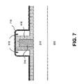
- a metal layer 710 such as nickel, may be deposited on the semiconductor device, as illustrated in FIG. 7 (act 130 ).
- nickel layer 710 may be deposited to a thickness of about 20 ⁇ to about 30 ⁇ .
- a metal-induced crystallization (MIC) operation may be performed.
- the MIC operation may include annealing nickel layer 710 at about 500° C. to about 550° C. for several hours, which acts to diffuse the nickel into the amorphous silicon of spacers 610 and to convert the amorphous silicon in spacers 610 to single-crystal or polycrystalline silicon fin structures 810 , as illustrated in FIG. 8 (act 135 ). In one implementation, the annealing occurs for about 1 to 5 hours.
- Undiffused portions of nickel layer 710 may be removed from the semiconductor device (act 140 ). The undiffused portions may be removed via etching or other well-known techniques.
- Portions of second SiO 2 layer 410 may then be removed, resulting in the configuration illustrated in FIG. 8 (act 145 ).
- the portions of second SiO 2 layer 410 located below fin structures 810 and on nitride layer 210 may be removed using a wet etch chemistry.
- the particular etchant(s) associated with etching second SiO 2 layer 410 may be optimized based on the particular end device requirements.
- a gap exits between fin structures 810 and nitride layer 210 . In one implementation, the gap may range from about 100 ⁇ to about 500 ⁇ .
- a gate dielectric layer may optionally be deposited or thermally grown on crystalline silicon fin structures 810 .
- the gate dielectric layer may be formed at a thickness ranging from approximately 5 ⁇ to 30 ⁇ .
- the gate dielectric layer may include conventional dielectric materials, such as an oxide (e.g., silicon dioxide).
- a nitride material such as a silicon nitride, may be used as the gate dielectric material.
- a gate material layer 910 may then be deposited and etched to form one or more gate electrodes, as illustrated in FIG. 9 (act 150 ).
- gate material layer 910 may include polysilicon deposited using conventional CVD to a thickness ranging from about 200 ⁇ to about 1000 ⁇ .
- other semiconducting materials such as germanium or combinations of silicon and germanium, or various metals may be used as the gate material.
- gate material layer 910 is patterned and etched to form three gate electrodes. First and second gate electrodes may be located on opposite sides adjacent the respective fin structures 810 and a third gate electrode may be located above fin structures 810 .
- Source/drain regions may be formed at the respective ends of fins 810 . It should be understood that in some implementations, source/drain regions may be formed at an earlier processing step.
- FIG. 10 illustrates an exemplary top view of the semiconductor device consistent with the principles of the invention after the source/drain regions and gate electrodes are formed. As illustrated, the semiconductor device includes a triple-gate structure with fins 810 , source and drain regions 1010 and 1020 , and gate electrodes 1030 , 1040 , and 1050 . Any one of gate electrodes 1030 , 1040 , and 1050 may be used to bias the semiconductor device during circuit operations.
- Source/drain regions 1010 and 1020 may then be doped with n-type or p-type impurities based on the particular end device requirements.
- sidewall spacers may optionally be formed prior to the source/drain ion implantation to control the location of the source/drain junctions based on the particular circuit requirements.
- Activation annealing may then be performed to activate source/drain regions 1010 and 1020 .
- the present invention has been described above as forming a tri-gate MOSFET with a number of fin structures. It should be understood that implementations consistent with the present invention may be used to form double or tri-gate devices with other numbers of fins, based on the particular circuit requirements.
- a tri-gate MOSFET device may be formed, providing better short-channel control than double and single gate devices. Also, the tri-gate MOSFET may have higher drive current than double-gate devices for the same gate area.
- FIGS. 11–14 illustrate exemplary views for forming a FinFET device in an alternative implementation consistent with the principles of the invention.
- the semiconductor device may include a silicon on insulator (SOI) structure with a buried oxide layer 1110 formed on a substrate 1100 and a silicon fin structure 1120 formed on buried oxide layer 1110 .
- Silicon fin structure 1120 may be formed via conventional techniques. For example, a photoresist material may be deposited and patterned to form a photoresist mask. The silicon layer may then be etched in a conventional manner, with the etching terminating on buried oxide layer 1110 , to form silicon fin structure 1120 .
- a metal layer 1210 may then be deposited on the semiconductor device, as illustrated in FIG. 12 .
- the metal layer 1210 may comprise tungsten, titanium, tantalum, or nickel. Other metals may alternatively be used.
- Metal layer 1210 may then be patterned and etched to form spacers 1310 , as illustrated in FIG. 13 . As illustrated, spacers 1310 are formed on opposite sides of silicon fin structure 1120 .
- a gate material layer 1410 may then be deposited to form one or more gate electrodes, as illustrated in FIG. 14 .
- gate material layer 1410 may include polysilicon deposited using conventional CVD. Alternatively, other semiconducting materials, such as germanium or combinations of silicon and germanium, or various metals may be used as the gate material.
- the gate material layer 1410 may then be patterned and etched to form gate electrodes. Metal spacers 1310 act to reduce the fin step height during gate patterning, thereby improving gate patterning.
- an alternative filling material may be used in fabricating a damascene gate MOSFET.
- a semiconductor device may include an oxide layer 1510 formed on a substrate (not shown) with a silicon layer 1520 formed thereon.
- a dummy polysilicon gate 1530 may be formed on silicon layer 1520 .
- a spacer material such as a silicon oxide (e.g., SiO 2 ), may be deposited and etched to form spacers 1540 on the side surfaces of dummy polysilicon gate 1530 .
- An organic material 1550 may then be deposited and planarized to expose the top surface of dummy polysilicon gate 1530 .
- Dummy polysilicon gate 1530 may then be removed.
- a metal gate 1610 may then be deposited and polished, as illustrated in FIG. 16 .
- the metal may include, for example, tungsten, tantalum nitride, tantalum silicon nitride, titanium, or nickel. Other metals may alternatively be used.
- Organic material 1550 may then be removed and the source and drain regions may be silicided 1620 .
- silicide 1620 may be NiSi or CoSi 2 .
- Implementations consistent with the principles of the invention provide a tri-gate MOSFET device that provides better short-channel control than double and single gate device designs.
Abstract
Description
Claims (16)
Priority Applications (1)
| Application Number | Priority Date | Filing Date | Title |
|---|---|---|---|
| US10/653,225 US6998301B1 (en) | 2003-09-03 | 2003-09-03 | Method for forming a tri-gate MOSFET |
Applications Claiming Priority (1)
| Application Number | Priority Date | Filing Date | Title |
|---|---|---|---|
| US10/653,225 US6998301B1 (en) | 2003-09-03 | 2003-09-03 | Method for forming a tri-gate MOSFET |
Publications (1)
| Publication Number | Publication Date |
|---|---|
| US6998301B1 true US6998301B1 (en) | 2006-02-14 |
Family
ID=35767881
Family Applications (1)
| Application Number | Title | Priority Date | Filing Date |
|---|---|---|---|
| US10/653,225 Expired - Fee Related US6998301B1 (en) | 2003-09-03 | 2003-09-03 | Method for forming a tri-gate MOSFET |
Country Status (1)
| Country | Link |
|---|---|
| US (1) | US6998301B1 (en) |
Cited By (27)
| Publication number | Priority date | Publication date | Assignee | Title |
|---|---|---|---|---|
| US20060091433A1 (en) * | 2004-10-29 | 2006-05-04 | Kazumi Nishinohara | Semiconductor integrated circuit device and manufacturing method thereof |
| US20060286755A1 (en) * | 2005-06-15 | 2006-12-21 | Brask Justin K | Method for fabricating transistor with thinned channel |
| US20070090408A1 (en) * | 2005-09-29 | 2007-04-26 | Amlan Majumdar | Narrow-body multiple-gate FET with dominant body transistor for high performance |
| US20070111419A1 (en) * | 2005-09-28 | 2007-05-17 | Doyle Brian S | CMOS Devices with a single work function gate electrode and method of fabrication |
| US20070152266A1 (en) * | 2005-12-29 | 2007-07-05 | Intel Corporation | Method and structure for reducing the external resistance of a three-dimensional transistor through use of epitaxial layers |
| US20070262389A1 (en) * | 2004-01-16 | 2007-11-15 | Robert Chau | Tri-gate transistors and methods to fabricate same |
| WO2007133775A2 (en) * | 2006-05-15 | 2007-11-22 | Carnegie Mellon University | Integrated circuit, device, system, and method of fabrication |
| US20080137051A1 (en) * | 2004-12-21 | 2008-06-12 | Carnegie Mellon University | Lithography and Associated Methods, Devices, and Systems |
| US20080142841A1 (en) * | 2004-03-31 | 2008-06-19 | Nick Lindert | Bulk non-planar transistor having strained enhanced mobility and methods of fabrication |
| US20080169512A1 (en) * | 2004-08-10 | 2008-07-17 | Doyle Brian S | Non-planar pMOS structure with a strained channel region and an integrated strained CMOS flow |
| US20080188041A1 (en) * | 2005-08-17 | 2008-08-07 | Suman Datta | Lateral undercut of metal gate in SOI device |
| US20080258207A1 (en) * | 2005-06-30 | 2008-10-23 | Marko Radosavljevic | Block Contact Architectures for Nanoscale Channel Transistors |
| US20090061572A1 (en) * | 2003-06-27 | 2009-03-05 | Intel Corporation | Nonplanar semiconductor device with partially or fully wrapped around gate electrode and methods of fabrication |
| US20090149012A1 (en) * | 2004-09-30 | 2009-06-11 | Brask Justin K | Method of forming a nonplanar transistor with sidewall spacers |
| US20090218603A1 (en) * | 2005-06-21 | 2009-09-03 | Brask Justin K | Semiconductor device structures and methods of forming semiconductor structures |
| US20090325350A1 (en) * | 2005-03-14 | 2009-12-31 | Marko Radosavljevic | Field effect transistor with metal source/drain regions |
| US20100297838A1 (en) * | 2004-09-29 | 2010-11-25 | Chang Peter L D | Independently accessed double-gate and tri-gate transistors in same process flow |
| US20110062512A1 (en) * | 2004-10-25 | 2011-03-17 | Uday Shah | Nonplanar device with thinned lower body portion and method of fabrication |
| US20110156145A1 (en) * | 2004-09-29 | 2011-06-30 | Marko Radosavljevic | Fabrication of channel wraparound gate structure for field-effect transistor |
| US7989280B2 (en) | 2005-11-30 | 2011-08-02 | Intel Corporation | Dielectric interface for group III-V semiconductor device |
| US8084818B2 (en) | 2004-06-30 | 2011-12-27 | Intel Corporation | High mobility tri-gate devices and methods of fabrication |
| US8183646B2 (en) | 2005-02-23 | 2012-05-22 | Intel Corporation | Field effect transistor with narrow bandgap source and drain regions and method of fabrication |
| US8362566B2 (en) | 2008-06-23 | 2013-01-29 | Intel Corporation | Stress in trigate devices using complimentary gate fill materials |
| US8405164B2 (en) | 2003-06-27 | 2013-03-26 | Intel Corporation | Tri-gate transistor device with stress incorporation layer and method of fabrication |
| CN103000527A (en) * | 2011-09-16 | 2013-03-27 | 中芯国际集成电路制造(上海)有限公司 | Multi-gate device manufacturing method |
| US8617945B2 (en) | 2006-08-02 | 2013-12-31 | Intel Corporation | Stacking fault and twin blocking barrier for integrating III-V on Si |
| KR101368509B1 (en) * | 2011-12-16 | 2014-02-27 | 타이완 세미콘덕터 매뉴팩쳐링 컴퍼니 리미티드 | Semiconductor device with biased feature |
-
2003
- 2003-09-03 US US10/653,225 patent/US6998301B1/en not_active Expired - Fee Related
Non-Patent Citations (5)
| Title |
|---|
| Digh Hisamoto et al., "FinFET-A Self-Aligned Double-Gate MOSFET Scalable to 20 nm," IEEE Transactions on Electron Devices, vol. 47, No. 12, Dec. 2000, pp. 2320-2325. |
| Xuejue Huang et al., "Sub 50-nm FinFET: PMOS," 1999 IEEE, IEDM, pp. 67-70. |
| Xuejue Huang et al., "Sub-50 nm P-Channel FinFET," IEEE Transactions on Electron Devices, vol. 48, No. 5, May 2001, pp. 880-886. |
| Yang-Kyu Choi et al., "Nanoscale CMOS Spacer FinFET for the Terabit Era," IEEE Electron Device Letters, vol. 23, No. 1, Jan. 2002, pp. 25-27. |
| Yang-Kyu Choi et al., "Sub-20nm CMOS FinFET Technologies," 2001 IEEE, IEDM, pp. 421-424. |
Cited By (70)
| Publication number | Priority date | Publication date | Assignee | Title |
|---|---|---|---|---|
| US7820513B2 (en) | 2003-06-27 | 2010-10-26 | Intel Corporation | Nonplanar semiconductor device with partially or fully wrapped around gate electrode and methods of fabrication |
| US8273626B2 (en) | 2003-06-27 | 2012-09-25 | Intel Corporationn | Nonplanar semiconductor device with partially or fully wrapped around gate electrode and methods of fabrication |
| US20090061572A1 (en) * | 2003-06-27 | 2009-03-05 | Intel Corporation | Nonplanar semiconductor device with partially or fully wrapped around gate electrode and methods of fabrication |
| US8405164B2 (en) | 2003-06-27 | 2013-03-26 | Intel Corporation | Tri-gate transistor device with stress incorporation layer and method of fabrication |
| US20070262389A1 (en) * | 2004-01-16 | 2007-11-15 | Robert Chau | Tri-gate transistors and methods to fabricate same |
| US7781771B2 (en) | 2004-03-31 | 2010-08-24 | Intel Corporation | Bulk non-planar transistor having strained enhanced mobility and methods of fabrication |
| US20080142841A1 (en) * | 2004-03-31 | 2008-06-19 | Nick Lindert | Bulk non-planar transistor having strained enhanced mobility and methods of fabrication |
| US8084818B2 (en) | 2004-06-30 | 2011-12-27 | Intel Corporation | High mobility tri-gate devices and methods of fabrication |
| US20080169512A1 (en) * | 2004-08-10 | 2008-07-17 | Doyle Brian S | Non-planar pMOS structure with a strained channel region and an integrated strained CMOS flow |
| US7960794B2 (en) | 2004-08-10 | 2011-06-14 | Intel Corporation | Non-planar pMOS structure with a strained channel region and an integrated strained CMOS flow |
| US8399922B2 (en) | 2004-09-29 | 2013-03-19 | Intel Corporation | Independently accessed double-gate and tri-gate transistors |
| US8268709B2 (en) | 2004-09-29 | 2012-09-18 | Intel Corporation | Independently accessed double-gate and tri-gate transistors in same process flow |
| US20110156145A1 (en) * | 2004-09-29 | 2011-06-30 | Marko Radosavljevic | Fabrication of channel wraparound gate structure for field-effect transistor |
| US20100297838A1 (en) * | 2004-09-29 | 2010-11-25 | Chang Peter L D | Independently accessed double-gate and tri-gate transistors in same process flow |
| US20090149012A1 (en) * | 2004-09-30 | 2009-06-11 | Brask Justin K | Method of forming a nonplanar transistor with sidewall spacers |
| US9741809B2 (en) | 2004-10-25 | 2017-08-22 | Intel Corporation | Nonplanar device with thinned lower body portion and method of fabrication |
| US8749026B2 (en) | 2004-10-25 | 2014-06-10 | Intel Corporation | Nonplanar device with thinned lower body portion and method of fabrication |
| US9190518B2 (en) | 2004-10-25 | 2015-11-17 | Intel Corporation | Nonplanar device with thinned lower body portion and method of fabrication |
| US8502351B2 (en) | 2004-10-25 | 2013-08-06 | Intel Corporation | Nonplanar device with thinned lower body portion and method of fabrication |
| US8067818B2 (en) | 2004-10-25 | 2011-11-29 | Intel Corporation | Nonplanar device with thinned lower body portion and method of fabrication |
| US20110062512A1 (en) * | 2004-10-25 | 2011-03-17 | Uday Shah | Nonplanar device with thinned lower body portion and method of fabrication |
| US10236356B2 (en) | 2004-10-25 | 2019-03-19 | Intel Corporation | Nonplanar device with thinned lower body portion and method of fabrication |
| US20060091433A1 (en) * | 2004-10-29 | 2006-05-04 | Kazumi Nishinohara | Semiconductor integrated circuit device and manufacturing method thereof |
| US8259286B2 (en) | 2004-12-21 | 2012-09-04 | Carnegie Mellon University | Lithography and associated methods, devices, and systems |
| US20080137051A1 (en) * | 2004-12-21 | 2008-06-12 | Carnegie Mellon University | Lithography and Associated Methods, Devices, and Systems |
| US8816394B2 (en) | 2005-02-23 | 2014-08-26 | Intel Corporation | Field effect transistor with narrow bandgap source and drain regions and method of fabrication |
| US8183646B2 (en) | 2005-02-23 | 2012-05-22 | Intel Corporation | Field effect transistor with narrow bandgap source and drain regions and method of fabrication |
| US10121897B2 (en) | 2005-02-23 | 2018-11-06 | Intel Corporation | Field effect transistor with narrow bandgap source and drain regions and method of fabrication |
| US9748391B2 (en) | 2005-02-23 | 2017-08-29 | Intel Corporation | Field effect transistor with narrow bandgap source and drain regions and method of fabrication |
| US9614083B2 (en) | 2005-02-23 | 2017-04-04 | Intel Corporation | Field effect transistor with narrow bandgap source and drain regions and method of fabrication |
| US9368583B2 (en) | 2005-02-23 | 2016-06-14 | Intel Corporation | Field effect transistor with narrow bandgap source and drain regions and method of fabrication |
| US9048314B2 (en) | 2005-02-23 | 2015-06-02 | Intel Corporation | Field effect transistor with narrow bandgap source and drain regions and method of fabrication |
| US8664694B2 (en) | 2005-02-23 | 2014-03-04 | Intel Corporation | Field effect transistor with narrow bandgap source and drain regions and method of fabrication |
| US8368135B2 (en) | 2005-02-23 | 2013-02-05 | Intel Corporation | Field effect transistor with narrow bandgap source and drain regions and method of fabrication |
| US20090325350A1 (en) * | 2005-03-14 | 2009-12-31 | Marko Radosavljevic | Field effect transistor with metal source/drain regions |
| US7879675B2 (en) | 2005-03-14 | 2011-02-01 | Intel Corporation | Field effect transistor with metal source/drain regions |
| US20060286755A1 (en) * | 2005-06-15 | 2006-12-21 | Brask Justin K | Method for fabricating transistor with thinned channel |
| US20110062520A1 (en) * | 2005-06-15 | 2011-03-17 | Brask Justin K | Method for fabricating transistor with thinned channel |
| US9337307B2 (en) | 2005-06-15 | 2016-05-10 | Intel Corporation | Method for fabricating transistor with thinned channel |
| US9806195B2 (en) | 2005-06-15 | 2017-10-31 | Intel Corporation | Method for fabricating transistor with thinned channel |
| US7858481B2 (en) * | 2005-06-15 | 2010-12-28 | Intel Corporation | Method for fabricating transistor with thinned channel |
| US9385180B2 (en) | 2005-06-21 | 2016-07-05 | Intel Corporation | Semiconductor device structures and methods of forming semiconductor structures |
| US8071983B2 (en) | 2005-06-21 | 2011-12-06 | Intel Corporation | Semiconductor device structures and methods of forming semiconductor structures |
| US8581258B2 (en) | 2005-06-21 | 2013-11-12 | Intel Corporation | Semiconductor device structures and methods of forming semiconductor structures |
| US8933458B2 (en) | 2005-06-21 | 2015-01-13 | Intel Corporation | Semiconductor device structures and methods of forming semiconductor structures |
| US9761724B2 (en) | 2005-06-21 | 2017-09-12 | Intel Corporation | Semiconductor device structures and methods of forming semiconductor structures |
| US20090218603A1 (en) * | 2005-06-21 | 2009-09-03 | Brask Justin K | Semiconductor device structures and methods of forming semiconductor structures |
| US20080258207A1 (en) * | 2005-06-30 | 2008-10-23 | Marko Radosavljevic | Block Contact Architectures for Nanoscale Channel Transistors |
| US7898041B2 (en) | 2005-06-30 | 2011-03-01 | Intel Corporation | Block contact architectures for nanoscale channel transistors |
| US20080188041A1 (en) * | 2005-08-17 | 2008-08-07 | Suman Datta | Lateral undercut of metal gate in SOI device |
| US7736956B2 (en) | 2005-08-17 | 2010-06-15 | Intel Corporation | Lateral undercut of metal gate in SOI device |
| US20110180851A1 (en) * | 2005-09-28 | 2011-07-28 | Doyle Brian S | Cmos devices with a single work function gate electrode and method of fabrication |
| US20070111419A1 (en) * | 2005-09-28 | 2007-05-17 | Doyle Brian S | CMOS Devices with a single work function gate electrode and method of fabrication |
| US7902014B2 (en) | 2005-09-28 | 2011-03-08 | Intel Corporation | CMOS devices with a single work function gate electrode and method of fabrication |
| US8294180B2 (en) | 2005-09-28 | 2012-10-23 | Intel Corporation | CMOS devices with a single work function gate electrode and method of fabrication |
| US20070090408A1 (en) * | 2005-09-29 | 2007-04-26 | Amlan Majumdar | Narrow-body multiple-gate FET with dominant body transistor for high performance |
| US7989280B2 (en) | 2005-11-30 | 2011-08-02 | Intel Corporation | Dielectric interface for group III-V semiconductor device |
| US20070152266A1 (en) * | 2005-12-29 | 2007-07-05 | Intel Corporation | Method and structure for reducing the external resistance of a three-dimensional transistor through use of epitaxial layers |
| WO2007133775A3 (en) * | 2006-05-15 | 2008-05-29 | Univ Carnegie Mellon | Integrated circuit, device, system, and method of fabrication |
| WO2007133775A2 (en) * | 2006-05-15 | 2007-11-22 | Carnegie Mellon University | Integrated circuit, device, system, and method of fabrication |
| US20090321830A1 (en) * | 2006-05-15 | 2009-12-31 | Carnegie Mellon University | Integrated circuit device, system, and method of fabrication |
| US8617945B2 (en) | 2006-08-02 | 2013-12-31 | Intel Corporation | Stacking fault and twin blocking barrier for integrating III-V on Si |
| US9450092B2 (en) | 2008-06-23 | 2016-09-20 | Intel Corporation | Stress in trigate devices using complimentary gate fill materials |
| US8362566B2 (en) | 2008-06-23 | 2013-01-29 | Intel Corporation | Stress in trigate devices using complimentary gate fill materials |
| US9806193B2 (en) | 2008-06-23 | 2017-10-31 | Intel Corporation | Stress in trigate devices using complimentary gate fill materials |
| US8741733B2 (en) | 2008-06-23 | 2014-06-03 | Intel Corporation | Stress in trigate devices using complimentary gate fill materials |
| US9224754B2 (en) | 2008-06-23 | 2015-12-29 | Intel Corporation | Stress in trigate devices using complimentary gate fill materials |
| CN103000527A (en) * | 2011-09-16 | 2013-03-27 | 中芯国际集成电路制造(上海)有限公司 | Multi-gate device manufacturing method |
| CN103000527B (en) * | 2011-09-16 | 2015-03-11 | 中芯国际集成电路制造(上海)有限公司 | Multi-gate device manufacturing method |
| KR101368509B1 (en) * | 2011-12-16 | 2014-02-27 | 타이완 세미콘덕터 매뉴팩쳐링 컴퍼니 리미티드 | Semiconductor device with biased feature |
Similar Documents
| Publication | Publication Date | Title |
|---|---|---|
| US6998301B1 (en) | Method for forming a tri-gate MOSFET | |
| US6645797B1 (en) | Method for forming fins in a FinFET device using sacrificial carbon layer | |
| US6709982B1 (en) | Double spacer FinFET formation | |
| US6762448B1 (en) | FinFET device with multiple fin structures | |
| EP1593150B1 (en) | Tri-gate and gate around mosfet devices and methods for making same | |
| TWI485848B (en) | Semiconductor device and method for fabricating the same | |
| US6833588B2 (en) | Semiconductor device having a U-shaped gate structure | |
| US6787439B2 (en) | Method using planarizing gate material to improve gate critical dimension in semiconductor devices | |
| US6686231B1 (en) | Damascene gate process with sacrificial oxide in semiconductor devices | |
| US6706571B1 (en) | Method for forming multiple structures in a semiconductor device | |
| US6787854B1 (en) | Method for forming a fin in a finFET device | |
| US6872647B1 (en) | Method for forming multiple fins in a semiconductor device | |
| US6764884B1 (en) | Method for forming a gate in a FinFET device and thinning a fin in a channel region of the FinFET device | |
| US8008136B2 (en) | Fully silicided gate structure for FinFET devices | |
| US7186599B2 (en) | Narrow-body damascene tri-gate FinFET | |
| US6815268B1 (en) | Method for forming a gate in a FinFET device | |
| US7416925B2 (en) | Doped structure for finfet devices | |
| US7498225B1 (en) | Systems and methods for forming multiple fin structures using metal-induced-crystallization | |
| US6995438B1 (en) | Semiconductor device with fully silicided source/drain and damascence metal gate | |
| US7091068B1 (en) | Planarizing sacrificial oxide to improve gate critical dimension in semiconductor devices | |
| US7432558B1 (en) | Formation of semiconductor devices to achieve <100> channel orientation | |
| US7029959B1 (en) | Source and drain protection and stringer-free gate formation in semiconductor devices | |
| KR20230004951A (en) | Horizontal gaa nano-wire and nano-slab transistors |
Legal Events
| Date | Code | Title | Description |
|---|---|---|---|
| AS | Assignment |
Owner name: ADVANCED MICRO DEVICES, INC., CALIFORNIA Free format text: ASSIGNMENT OF ASSIGNORS INTEREST;ASSIGNORS:YU, BIN;AHMED, SHIBLY S.;REEL/FRAME:014466/0391;SIGNING DATES FROM 20030220 TO 20030307 |
|
| FEPP | Fee payment procedure |
Free format text: PAYOR NUMBER ASSIGNED (ORIGINAL EVENT CODE: ASPN); ENTITY STATUS OF PATENT OWNER: LARGE ENTITY |
|
| FPAY | Fee payment |
Year of fee payment: 4 |
|
| AS | Assignment |
Owner name: GLOBALFOUNDRIES INC., CAYMAN ISLANDS Free format text: AFFIRMATION OF PATENT ASSIGNMENT;ASSIGNOR:ADVANCED MICRO DEVICES, INC.;REEL/FRAME:023119/0083 Effective date: 20090630 |
|
| FPAY | Fee payment |
Year of fee payment: 8 |
|
| FEPP | Fee payment procedure |
Free format text: MAINTENANCE FEE REMINDER MAILED (ORIGINAL EVENT CODE: REM.) |
|
| LAPS | Lapse for failure to pay maintenance fees |
Free format text: PATENT EXPIRED FOR FAILURE TO PAY MAINTENANCE FEES (ORIGINAL EVENT CODE: EXP.) |
|
| STCH | Information on status: patent discontinuation |
Free format text: PATENT EXPIRED DUE TO NONPAYMENT OF MAINTENANCE FEES UNDER 37 CFR 1.362 |
|
| FP | Lapsed due to failure to pay maintenance fee |
Effective date: 20180214 |
|
| AS | Assignment |
Owner name: GLOBALFOUNDRIES U.S. INC., NEW YORK Free format text: RELEASE BY SECURED PARTY;ASSIGNOR:WILMINGTON TRUST, NATIONAL ASSOCIATION;REEL/FRAME:056987/0001 Effective date: 20201117 |