US6995437B1 - Semiconductor device with core and periphery regions - Google Patents
Semiconductor device with core and periphery regions Download PDFInfo
- Publication number
- US6995437B1 US6995437B1 US10/869,774 US86977404A US6995437B1 US 6995437 B1 US6995437 B1 US 6995437B1 US 86977404 A US86977404 A US 86977404A US 6995437 B1 US6995437 B1 US 6995437B1
- Authority
- US
- United States
- Prior art keywords
- layer
- region
- hard mask
- core
- semiconductor device
- Prior art date
- Legal status (The legal status is an assumption and is not a legal conclusion. Google has not performed a legal analysis and makes no representation as to the accuracy of the status listed.)
- Expired - Lifetime, expires
Links
Images


Classifications
-
- H—ELECTRICITY
- H01—ELECTRIC ELEMENTS
- H01L—SEMICONDUCTOR DEVICES NOT COVERED BY CLASS H10
- H01L27/00—Devices consisting of a plurality of semiconductor or other solid-state components formed in or on a common substrate
- H01L27/02—Devices consisting of a plurality of semiconductor or other solid-state components formed in or on a common substrate including semiconductor components specially adapted for rectifying, oscillating, amplifying or switching and having at least one potential-jump barrier or surface barrier; including integrated passive circuit elements with at least one potential-jump barrier or surface barrier
- H01L27/04—Devices consisting of a plurality of semiconductor or other solid-state components formed in or on a common substrate including semiconductor components specially adapted for rectifying, oscillating, amplifying or switching and having at least one potential-jump barrier or surface barrier; including integrated passive circuit elements with at least one potential-jump barrier or surface barrier the substrate being a semiconductor body
- H01L27/10—Devices consisting of a plurality of semiconductor or other solid-state components formed in or on a common substrate including semiconductor components specially adapted for rectifying, oscillating, amplifying or switching and having at least one potential-jump barrier or surface barrier; including integrated passive circuit elements with at least one potential-jump barrier or surface barrier the substrate being a semiconductor body including a plurality of individual components in a repetitive configuration
- H01L27/105—Devices consisting of a plurality of semiconductor or other solid-state components formed in or on a common substrate including semiconductor components specially adapted for rectifying, oscillating, amplifying or switching and having at least one potential-jump barrier or surface barrier; including integrated passive circuit elements with at least one potential-jump barrier or surface barrier the substrate being a semiconductor body including a plurality of individual components in a repetitive configuration including field-effect components
-
- H—ELECTRICITY
- H10—SEMICONDUCTOR DEVICES; ELECTRIC SOLID-STATE DEVICES NOT OTHERWISE PROVIDED FOR
- H10B—ELECTRONIC MEMORY DEVICES
- H10B43/00—EEPROM devices comprising charge-trapping gate insulators
- H10B43/30—EEPROM devices comprising charge-trapping gate insulators characterised by the memory core region
-
- H—ELECTRICITY
- H10—SEMICONDUCTOR DEVICES; ELECTRIC SOLID-STATE DEVICES NOT OTHERWISE PROVIDED FOR
- H10B—ELECTRONIC MEMORY DEVICES
- H10B43/00—EEPROM devices comprising charge-trapping gate insulators
- H10B43/40—EEPROM devices comprising charge-trapping gate insulators characterised by the peripheral circuit region
Definitions
- the present invention generally relates to the manufacture of semiconductor devices and, more specifically, relates to manufacturing semiconductor devices by forming core and periphery gates including two critical masking steps to form a hard mask in a core region that includes a critical dimension less than achievable at a resolution limit of lithography.
- lithographic tools such as 1:1 optical projection systems fitted with deep-ultraviolet source and optics.
- new photoresist materials have been introduced.
- new processes have been developed, such as a multilayer resist utilizing a top resist sensitized to X-ray or electron-beam and a bottom straight optical resist layer(s).
- an invention which forms a line and space pattern including variable critical dimensions on a substrate sub-divided into regions. Further, there is a need for an invention that forms a line and space pattern in one region that includes a first feature comprising a first critical dimension different than a second critical dimension of a second feature in another region of the substrate. Further, there is a need to form one of the features to include a critical dimension less than achievable at a resolution limit of lithography. Additionally, there is a need for an invention that saves steps in a manufacturing process by reducing the number of steps used to form a mask used in the process. Additionally, there exists a need for an invention that forms gates and spaces comprising different critical dimensions in the regions of the substrate that reduces the processing steps required to form the gates and spaces.
- the invention is a method of forming a layer comprising a line and space pattern over a substrate including a first region and a second region, the method comprising the steps of:
- the invention is a method of patterning a layer on a substrate including a first region and a second region, the method comprising the steps of:
- the invention is a semiconductor device, comprising:
- FIG. 1 is a cross-section of a patterned layer on a substrate including a pattern of opening(s) including a dimension less than achievable by a resolution limit of lithography in a first region and a line(s) including a lateral dimension achievable by lithography in a second region, according to an embodiment of the present invention
- FIGS. 2–6 are sequential cross-sections of a method of manufacturing the patterned layer according to the present invention at intermediate stages of manufacture.
- FIG. 7 is a flow diagram of a method of manufacturing the patterned layer according to the present invention.
- the present invention comprises a layer, including a line and space pattern, disposed over a substrate or wafer.
- the substrate includes at least two regions, e.g., a first region and a second region.
- the first region may be a core region, whereas the second region may be a periphery region.
- the line and space pattern over the first region or core region includes a first line and space sub-pattern comprising a first feature including a first critical dimension less than achievable at a resolution limit of lithography.
- the first feature may be a space including, e.g., a lateral dimension as the first critical dimension.
- the line and space pattern over the second region or periphery region includes a second line and space sub-pattern comprising a second feature including a second critical dimension that is determined by a device parameter.
- the second feature may be a line including, e.g., a lateral dimension as the second critical dimension.
- the second critical dimension is achievable at a resolution limit of lithography.
- the layer includes a line and space pattern comprising varying pitch and critical dimensions.
- the present invention includes a method of patterning a layer comprising varying pitch and critical dimensions on a substrate or wafer including at least two regions, e.g., a first region and a second region.
- the method uses two critical masking steps to form a hard mask.
- the hard mask includes a master line and space pattern comprising varying pitch and critical dimensions.
- Over the first region the hard mask includes a first master line and space sub-pattern including at least one space comprising a first critical dimension less than a minimum dimension achievable at a resolution limit of lithography.
- the hard mask includes a second master line and space sub-pattern including at least one line comprising a second critical dimension.
- the second critical dimension is achievable by lithography processes alone.
- the hard mask line and space pattern is transferred to the layer using a single etch step.
- a semiconductor device is formed using a method further described below.
- the conductive layer is patterned to form gates in the first region (e.g., a core region) and the second region (e.g., a periphery region) including varying pitch and critical dimensions.
- the method provides a means for reducing the space between the gates (e.g., core gates) in the core region by increasing the lateral dimensions of the gates in the core region.
- the gates (e.g., periphery gates) and spaces formed in the periphery region include a lateral dimension achievable by lithography.
- the line and space pattern including variable pitch and critical dimensions i.e., reduced space between the core gates and the lateral dimensions of the periphery gates achievable by lithography processes alone, resulting from the method significantly increase the performance of the semiconductor device while reducing the manufacturing cost thereof.
- a layer to be patterned is formed over the substrate.
- the first mask layer includes a high temperature oxide (HTO).
- HTO high temperature oxide
- ARC anti-reflective coating
- SiRN silicon rich nitride
- a first layer of photosensitive material is applied.
- the first layer of photosensitive material is patterned by lithographic means to form a first lithographic image.
- the first lithographic image includes lines and spaces in the first layer of photosensitive material in the first region.
- the lines and spaces include a minimum dimension dictated by a resolution limit of lithography.
- the first lithographic image is transferred to the first mask layer by an etch process, e.g., a plasma etch process.
- a first hard mask is produced including a master line and space sub-pattern in the first region.
- the master line and space sub-pattern includes lines and spaces including the minimum dimension dictated by the resolution limit of lithography.
- an etch process e.g., a directional reactive ion etching (RIE) is performed to remove the remaining first layer of photosensitive material.
- RIE reactive ion etching
- a conformal second mask layer is applied to the exposed surfaces of the first mask layer and the layer resulting from the transfer of the first lithographic image.
- the thickness of the conformal second mask layer is determined by the desired reduction in the size of the spaces in the first hard mask in the first region. For example, for an elongated opening (space), the reduction in the width of the space is approximately twice the thickness of the conformal second mask layer.
- the conformal second mask layer may be HTO, e.g., formed by chemical vapor deposition (CVD), plasma enhanced chemical vapor deposition (PECVD) or other processes known by those having ordinary skill in the art.
- a second layer of photosensitive material is applied to the conformal second mask layer.
- the second layer of photosensitive material is now patterned by lithographic means to form a second lithographic image.
- the second lithographic image includes lines and spaces in the second layer of photosensitive material in the second region.
- the lines and spaces include a dimension dictated by a device parameter.
- the dimension may be a minimum dimension achievable at the resolution limit of lithography.
- the pattern of lines and spaces in the second layer of photosensitive material in the second region may include a critical dimension of any dimension producible by lithography processes alone. The critical dimension is dictated by desired device parameters.
- the second lithographic image is transferred to the first mask layer. The transfer produces lines and spaces in the first mask layer in the second region of a dimension dictated by the device parameter.
- an etch process e.g., an RIE
- Another etch process for example, another RIE using a different etchant species, is used to remove portions of the conformal second mask layer from the horizontal surfaces of the ARC and portions of the horizontal surfaces of the layer exposed by the spaces.
- the RIE leaves portions of the conformal second mask layer on the non-horizontal surfaces corresponding to the sidewalls of the lines in the first hard mask layer in the first region.
- the remaining portions are more commonly referred to as hard mask spacers.
- the ARC exposed by the etch process in the first and second regions may be removed by another etch process selective to the ARC.
- an ARC strip may be performed to remove the remaining ARC material. It should be understood by those having ordinary skill in the art that removal of the ARC at this time is optional. If the ARC is not removed, then the ARC functions as part of the hard mask.
- the first hard mask including the hard mask spacers in the first region and without sidewall spacers in the second region constitutes a new mask (a second hard mask or stencil).
- the new mask includes spaces with a critical dimension less than obtainable by lithography processes alone.
- the new mask is unbiased by sidewall spacers.
- the new mask can be used to transfer the line and space pattern to the layer using a single etch step.
- the new mask may be used to form gates and spaces in the first region comprising a space including a critical dimension less than achievable by the resolution limit of lithography. Further, the new mask may be used to form gates and spaces in the second region comprising a gate including a critical dimension dictated by a device parameter achievable by lithography.
- the new mask can be used for a variety of other purposes, including ion implantation to implant the layer or the substrate through an intervening layer(s). Alternatively, if the substrate is exposed, the substrate may be implanted directly. Further, the new mask may be used as an etch mask to etch narrow trenches in an underlying layer(s), substrate or both. Further still, the new mask may be used as an oxidation mask to form recessed oxide isolation in the exposed regions of the layer or substrate. Additionally, the new mask may be used as a contact mask to establish narrow dimensioned contacts on the layer or exposed regions of the substrate, etc.
- the new mask may be removed from the layer by subjecting the new mask to a wet or dry etchant.
- the structure includes at least one gate stack structure of a typical gate, e.g., metal on semiconductor field effect transistor (MOSFET), floating gate (FG), semiconductor oxide-nitride-oxide semiconductor (SONOS) gate or the like, then conventional processes may be used to complete the semiconductor device(s).
- MOSFET metal on semiconductor field effect transistor
- FG floating gate
- SONOS semiconductor oxide-nitride-oxide semiconductor
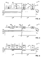
- a structure of the present invention is shown, generally designated as 10 .
- the structure 10 will be described below in relationship to a semiconductor device 10 .
- the structure 10 is also referred to herein as the semiconductor device 10 , those having ordinary skill in the art will appreciate that the invention applies more generally to the formation on a substrate of a feature including a lateral dimension or critical dimension (CD) less than the CD achievable at the resolution limit of lithography in one region and a feature including a CD that is achievable at the resolution limit of lithography in another region.
- CD critical dimension
- the semiconductor device 10 includes a substrate 12 , including a first region 14 and a second region 16 .
- the substrate 12 also includes an active region in a surface region of the substrate (not shown), e.g., a p-type doped region.
- a layer 18 including a line and space pattern 20 , is formed.
- a dielectric layer 22 is interposed between the layer 18 and the substrate 12 .
- the line and space pattern 20 includes gate electrodes 18 a and 18 b and space(s) 24 .
- the space(s) 24 between the gates 18 a and 18 b in the first region 14 includes a dimension A that is less than a minimum dimension achievable by a resolution limit of lithography.
- the gates 18 c and 18 d in the second region 16 include a lateral dimension achievable by lithography and dictated by a device parameter.
- the lateral dimension B is a minimum dimension achievable by the resolution limit of lithography.
- the semiconductor device 10 may include gates comprising conventional gate stack structures.
- a SONOS gate structure is illustrated in the first region 14 .
- the SONOS gate structure includes a dielectric layer 22 a , e.g., an oxide-nitride-oxide (ONO) layer, interposed between gate electrodes 18 a and 18 b and the substrate 12 .
- a MOSFET structure is illustrated in the second region 16 .
- the MOSFET includes a dielectric layer 22 b interposed between gate electrodes 18 c and 18 d and the substrate 12 .
- a floating gate structure including a dielectric layer, a charge-trapping layer, an ONO layer and a control gate may be formed (not shown).
- the layer 18 may be of a conductor, a semiconductor, or an insulator material or a combination thereof as will be further described below.
- the layer 18 is polysilicon.
- the layer 18 may have a thickness of between about 5 nm and about 200 nm.
- the layer 18 is illustrated in FIG. 1 as a single layer, however, the layer 18 could be multiple layers.
- the dielectric layer 22 a in the first region 14 may also be referred to herein as a charge-trapping dielectric layer 22 a .
- the charge-trapping dielectric layer 22 a may include a tunneling layer 28 , a charge-trapping layer 30 and an insulating layer 32 .
- the tunneling layer 28 is interposed between the charge-trapping layer 30 and the substrate 12 .
- the charge-trapping layer 30 is interposed between the insulating layer 32 and the tunneling layer 28 .
- the insulating layer 32 is interposed between the layer 18 and the charge-trapping layer 30 .
- the tunneling layer 28 , the charge-trapping layer 30 and the insulating layer 32 may be an oxide-nitride-oxide (ONO) layer, typical of a SONOS gate structure.
- the tunneling layer 28 and/or the insulating layer 32 may be of a high-K material as will be further described below.
- the dielectric layer 22 a may have a thickness of between about 1 nm and about 10 nm.
- the dielectric layer 22 a may have a thickness of, for example, between about 2 nm and about 8 nm. In another embodiment, the dielectric layer 22 a may have a thickness of, for example, between about 3 nm and about 7 nm. It should be understood by those having ordinary skill in the art that the above thicknesses are merely exemplary and that the thicknesses may be combined, for example, from about 1 nm to about 7 nm, or about 2 nm to about 10 nm, or about 2 nm to about 7 nm or the like.
- the dielectric layer 22 b in the second region 16 may also be referred to herein as a gate dielectric layer 22 b .
- the gate dielectric layer 22 b may comprise a single layer or multiple layers. Further, the gate dielectric layer 22 b may be of conventional dielectric material or of a high-K material as will be further described below.
- the dielectric layer 22 b may have a thickness of between about 1 nm and about 10 nm.
- the dielectric layer 22 b may have a thickness of, for example, between about 2 nm and about 8 nm. In another embodiment, the dielectric layer 22 b may have a thickness of, for example, between about 3 nm and about 7 nm. It should be understood by those having ordinary skill in the art that the above thicknesses are merely exemplary and that the thicknesses may be combined, for example, from about 1 nm to about 7 nm, or about 2 nm to about 10 nm, or about 2 nm to about 7 nm or the like.
- the substrate 12 may be of a conductor, a semiconductor, or an insulator material or a combination thereof, as will be further described below.
- the substrate 12 may have a thickness of between about 50 nm and about 2,000 nm.
- the sidewall spacers 46 d may be of a hard mask material further described below.
- the sidewall spacers 46 d are of a HTO, for example.
- the sidewall spacers 46 d may have a thickness between about 5 nm and about 50 nm and a height between about 5 nm and about 150 nm.
- the sidewall spacers 46 d are illustrated in FIGS. 5 and 6 as a homogeneous composition, however, the sidewall spacers 46 d could comprise multiple layers or have a graded composition.
- the illustrated device is a semiconductor device comprising a layer patterned with varying pitch and critical dimensions
- other devices can also be improved using the method to pattern a layer on a substrate including variable pitch and critical dimensions as further described herein.
- FIGS. 2–6 illustrates various steps of the method 210 . It will be appreciated that the method 210 and the semiconductor device 10 described below are merely exemplary, and that suitable embodiments of the many above-described variations in materials, thicknesses, and/or structures may alternatively be used in the method 210 and/or the semiconductor device 10 .
- Step 212 a structure representing an intermediate step of the manufacturing process of the semiconductor device 10 is shown.
- the method is initiated with a substrate 12 .
- the substrate 12 may be of any substrate material.
- the substrate 12 may be a conductor, a semiconductor, a compound semiconductor or an insulator material, for example, metal, silicon, GaAs, InGaAs, silicon oxide, glass, photosensitive material or a combination thereof.
- the substrate 12 may include at least one of silicon, germanium, silicon-germanium alloys, silicon-carbon alloys, silicon-germanium alloys containing carbon, and other conductive and semi-conductive materials; the aforementioned materials implanted with any element; the aforementioned materials in layered or graded composition combinations; the aforementioned materials in porous; amorphous, single crystal, polycrystalline, nanocrystalline form; and mixtures thereof.
- a dielectric layer 22 of one or more layers is formed, grown, deposited, spin coated or the like, or a combination thereof, on the semiconductor substrate 12 using known techniques. For example, a PVD, a PECVD or a CVD process appropriate for the layer being deposited may apply the dielectric layer 22 .
- the dielectric layer 22 includes a charge-trapping dielectric layer 22 a formed over the first region 14 and a gate dielectric layer 22 b formed over the second region 16 .
- the charge-trapping dielectric layer 22 a includes a tunneling layer 28 , a charge-trapping layer 30 and an insulating layer 32 .
- the gate dielectric layer 22 b is illustrated as a single layer; however, it may be comprised of multiple layers.
- the tunneling layer 28 and the insulating layer 32 may be of a conventional dielectric material, e.g., Si x O y or of a high-K dielectric material, as further described above.
- the charge-trapping layer 30 may be of any material that is compatible with the first and second dielectric layers and is capable of storing a charge.
- the charge-trapping layer 30 may be a nitride, e.g., silicon nitride, silicon oxynitride or the like.
- the dielectric layer 22 may have a thickness of between, for example, about 1 nm and about 250 nm.
- each sub-layer will be deposited to a thickness according to a desired device parameter for a semiconductor device 10 to be realized.
- the charge-trapping dielectric layer 22 a may comprise only two layers, e.g., the tunneling layer 32 and the charge-trapping layer 34 .
- the layer 18 is formed, grown, deposited, spin coated or the like, or a combination thereof, on the dielectric layer 22 using known techniques.
- the layer 18 may be deposited over the dielectric layer 22 by chemical vapor deposition (CVD), plasma enhanced chemical vapor deposition (PECVD), atomic layer deposition (ALD) or the like.
- CVD chemical vapor deposition
- PECVD plasma enhanced chemical vapor deposition
- ALD atomic layer deposition
- the layer 18 may be of any material desired to be patterned.
- the layer 18 may be of non-conductive material, conductive material, semiconductive material, dielectric material or a combination thereof.
- the layer 18 comprises at least one of silicon, germanium, silicon-germanium alloys, silicon-carbon alloys, silicon-germanium alloys containing carbon, GaAs, InGaAs, and other conductive and semi-conductive materials; silicon oxide (Si x O y ), silicon-dioxide (SiO 2 ), aluminum oxide (Al 2 O 3 ), hafnium oxide (HfO), zirconium oxide (ZrO), titanium oxide (TiO), yttrium oxide (YO), lanthanum oxide (La 2 O 3 ), cerium oxide (CeO 2 ), bismuth silicon oxide (Bi 4 Si 2 O 12 ), tantalum oxide (Ta 2 O 5 ), tungsten oxide (WO 3 ), LaAlO 3 , BST (Ba 1-x Sr
- Permittivity, ⁇ , of a material reflects the ability of the material to be polarized by an electric field.
- the permittivity of a material is typically described as its permittivity normalized to the permittivity of a vacuum, ⁇ o .
- silicon-dioxide (sometimes simply referred to as “oxide”) has a dielectric constant of approximately 3.9
- other materials have higher K values.
- aluminum oxide (Al 2 O 3 ) has a K of about 9 to about 10.
- Much higher K values of, for example, 20 or more, can be obtained with various transition metal oxides, including tantalum oxide (Ta 2 O 5 ), hafnium oxide (HfO 2 ) and zirconium oxide (ZrO 2 ).
- a dielectric material including a higher K for the gate dielectric allows a high capacitance and an electrical equivalent thickness of a thinner silicon-dioxide (SiO 2 ) gate dielectric layer to be achieved while maintaining or increasing the physical thickness of the gate dielectric.
- SiO 2 silicon-dioxide
- an aluminum oxide (Al 2 O 3 ) layer that includes a K of 9.6 and a physical thickness of 6.25 nm substantially electrically equivalent to a silicon oxide (SiO 2 ) layer (K 3.9) including a physical thickness of 2.5 nm. Therefore, the gate dielectric can be made electrically thin while being formed of a physically thicker layer compared to conventional SiO 2 gate dielectric layer.
- dielectric material including a high K examples include the following: aluminum oxide (Al 2 O 3 ), hafnium oxide (HfO 2 ), zirconium oxide (ZrO 2 ), zirconium oxide (ZrO), titanium oxide (TiO), yttrium oxide (YO), zirconium silicate, hafnium silicate, lanthanum oxide (La 2 O 3 ), cerium oxide (CeO 2 ), bismuth silicon oxide (Bi 4 Si 2 O 12 ), tantalum oxide (Ta 2 O 5 ), tungsten oxide (WO 3 ), LaAlO 3 , BST (Ba 1-x Sr x TiO 3 ), PbTiO 3 , BaTiO 3 , SiTiO 3 , PbZrO 3 , PST (PbSc x Ta 1-x O 3 ), PZN (PbZn x Nb 1-x O 3 ), PZT (PbZr x Ti 1-x O 3 ), PMN (P
- the layer 18 is of a polysilicon.
- the polysilicon may be deposited on the substrate 12 using a PECVD process.
- the layer 18 may have a thickness, for example, between about 5 nm to about 1,000 nm thick.
- a first hard mask layer 34 is formed, grown, deposited, spin coated or the like, or a combination thereof, on the layer 18 again using conventional techniques.
- the first hard mask layer 34 may be thermally grown by conventional techniques.
- the first hard mask layer 34 may be deposited using conventional techniques.
- the first hard mask layer 34 may be formed using a combination of the above, e.g., a thin oxide layer may be thermally grown to form a good interface and then an oxide of lesser quality may be deposited thereon.
- the first hard mask layer 34 may be of any known mask material.
- the first hard mask layer 34 is formed of a high temperature oxide material (HTO).
- HTO high temperature oxide material
- the first hard mask layer 34 may have a thickness of between about 5 nm and about 1,000 nm, for example.
- the first hard mask layer material may also comprise at least one of silicon oxide, Si x O y , silicon-dioxide (SiO 2 ), other oxides; silicon nitride (Si x N y ), silicon rich nitride, oxygen rich nitride, other nitrides; the aforementioned materials implanted with any element; the aforementioned materials in layered or graded composition combinations; the aforementioned materials in porous, amorphous or nanocrystalline form; and mixtures thereof.
- an anti-reflective coating (ARC) 36 is applied, for example, by CVD.
- the ARC 36 comprises silicon rich nitride (SiRN).
- SiRN silicon rich nitride
- the ARC 36 may have a thickness in the range of about 10 nm to about 500 nm, for example.
- the ARC 36 material may also comprise at least one of silicon oxide, Si x O y , silicon-dioxide (SiO 2 ), silicon rich oxide (SiRO), other oxides; silicon nitride (Si x N y ), SiRN, oxygen rich nitride, other nitrides; silicon carbide (Si x C y ), other carbides; amorphous carbon, spin on organic ARC material; the aforementioned materials implanted with any element; the aforementioned materials in layered or graded composition combinations; the aforementioned materials in porous, amorphous or nanocrystalline form; and mixtures thereof.
- the ARC 36 is optional. However, the ARC 36 is used when increased resolution of the lithography process is required.
- a first photosensitive layer 38 of a photosensitive material is applied over the ARC 36 , for example, by spin-coating.
- the first photosensitive layer 38 may have a thickness in the range of about 30 nm to about 500 nm, for example.
- the first photosensitive layer 38 is a photoresist selective to the first hard mask layer 34 or the ARC 36 , if an ARC is used. That is, the photoresist is compatible with the first hard mask layer 34 and when processed, can be used as an etch mask to etch a lithographic image into the first hard mask layer 34 .
- the first photosensitive layer 38 is patterned (i.e., patterned to form sub-first photosensitive layers 38 a – 38 c , i.e., a lithographic image) by pattern-exposing using a conventional lithographic tool, developed, rinsed and dried.
- an anisotropic etching is conducted to form an opening(s) 40 , also referred to as spaces, in the first photosensitive layer 38 according to the pattern.
- an opening(s) 40 also referred to as spaces
- FIG. 2 only two openings 40 and two lines (sub-first photosensitive layers 38 a and 38 b ) are shown in the first region 14 .
- the two lines 38 a and 38 b include substantially vertical surfaces.
- the opening 40 between the two lines 38 a and 38 b include a lateral dimension C.
- the dimension C represents, for example, the minimum dimension that is obtainable at the resolution limit of the lithography processes utilized in Step 220 . That is, the dimension C may be the smallest dimension that is achievable by pushing known lithography (including x-ray, electron-beam or the like) to its highest resolution limit. This is considered the first critical masking step.
- the patterned sub-first photosensitive layers 38 a – 38 c are subjected to a hardening process step to thermally stabilize the patterned sub-first photosensitive layers 38 a – 38 c .
- Deep ultraviolet exposure or heat treatment at a temperature of about 200° C. to about 250° C. for about 1–2 minutes may be used for hardening.
- the patterned sub-first photosensitive layers 38 a – 38 c may be hardened by subjecting the patterned sub-first photosensitive layers 38 a – 38 c to a halogen gas plasma.
- the hardening step is needed for conventional photoresists, lest the photosensitive material constituting the patterned sub-first photosensitive layers 38 a – 38 c may melt and flow or otherwise get degraded during the subsequent processes.
- the hardening of the photoresistant material may not be required for photoresistant material including a higher melting point as will be understood by those having ordinary skill in the art.
- Step 224 an anisotropic etch is conducted to transfer the lithographic image of the patterned sub-first photosensitive layers 38 a – 38 c to the first hard mask layer 34 in the first region 14 .
- An etchant removes the ARC 36 exposed by the openings 40 and the first hard mask layer 34 beneath the exposed ARC 36 .
- the etch step leaves openings 42 including a lateral dimension D in the patterned first hard mask layer 34 .
- the line/space ratio in the first region 14 may be, for example, from about 0.07 ⁇ m/0.09 ⁇ m. In another embodiment, the line/space ratio in the first region 14 may be, for example, from about 0.10 ⁇ m/0.15 ⁇ m.
- the line/space ratio in the first region 14 may be, for example, from about 0.12 ⁇ m/0.19 ⁇ m. In other words, for a specific pitch, e.g., 160 nm, 250 nm or 310 nm, a line is about 40% of the pitch.
- the resultant structures include a first vertical stack ( 34 a , 36 a , 38 a ) and a second vertical stack ( 34 b , 36 b , 38 b ) in the first region 14 and a third vertical stack ( 34 c , 36 c , 38 c ) covering in the second region 16 .
- the first vertical stack ( 34 a , 36 a , 38 a ) includes a sub-first hard mask layer 34 a , a sub-ARC layer 36 a and a sub-first photosensitive layer 38 a .
- the second vertical stack ( 34 b , 36 b , 38 b ) includes a sub-first hard mask layer 34 b , a sub-ARC layer 36 b and a sub-photosensitive layer 38 b .
- the third vertical stack ( 34 c , 36 c , 38 c ) includes a sub-first hard mask layer 34 c , a sub-ARC layer 36 c and a sub-first photosensitive layer 38 c.
- Openings 42 formed in the first hard mask layer 34 as a result of the transfer include substantially vertical surfaces 44 .
- the dimension D is approximately equal to dimension C (shown in FIG. 2 ).
- a subsequent anisotropic etching removes the remaining photosensitive material of the first photosensitive layer 38 , i.e., the sub-first photosensitive layers 38 a – 38 c .
- the lithographic image is transferred from the patterned first photosensitive layer 38 to the first hard mask layer 34 in the first region 14 .
- Steps 228 and 232 sidewalls are formed on the vertical surfaces 44 of the sub-first hard mask layers 34 a and 34 b and the sub-ARC layers 36 a and 36 b in the first region 14 to reduce by a lateral dimension E ( FIG. 5 ) the openings 42 ( FIG. 3 ).
- the third vertical stack ( 34 c , 36 c , 38 c ) in the second region 16 is patterned and etched to form lines 50 in the sub-first hard mask layer 34 c in the second region 16 .
- the lines 50 include a width dimension achievable using lithography.
- a conformal second hard mask layer is formed over the substrate 12 .
- the conformal second hard mask layer 46 is formed over the patterned sub-first hard mask layers 34 a – 34 c , the sub-ARC layers 36 a – 36 c and the portion of the layer 18 exposed by the openings 42 (see FIG. 3 ).
- the conformal second hard mask layer 46 may be any material that can be deposited on the patterned sub-first hard mask layers 34 a – 34 c , the sub-ARC layers 36 a – 36 c and the layer 18 exposed in the openings 42 .
- Examples of conformal second hard mask layer material include the materials described above associated with the first hard mask layer 34 .
- the conformal second hard mask layer 46 may be of the same material as the first hard mask layer 34 .
- the conformal second hard mask layer 46 is Si x O y obtained by hexamethyldisilazane (HMDS) plasma deposition.
- the conformal second hard mask layer 46 is formed by mounting the substrate 12 in a plasma deposition system. Then, liquid HMDS is introduced into the process chamber and the necessary electric field is generated therein which transforms the liquid HMDS into a HMDS plasma. The HMDS plasma will be deposited on the structure until a uniform conformal second hard mask layer 46 of plasma-deposited HMDS, including the composition Si x O y , is obtained.
- the thickness of conformal second hard mask layer 46 is determined by the desired reduction in the lithographic image size in the first hard mask layer 34 .
- the thickness of the conformal second hard mask layer 46 is in a range of about 3 nm to about 900 nm.
- the thickness may be in a range of about 10 nm to about 100 nm.
- the thickness may be in a range of about 30 nm to about 50 nm.
- the above thicknesses are merely exemplary and that the thicknesses may be combined, for example, from about 3 nm to about 50 nm, or about 10 nm to about 30 nm, or about 30 nm to about 100 nm or the like.
- the lower limit for the thickness of the conformal second hard mask layer 46 is dictated by the requirements of good step coverage associated with the substantially vertical wall profile in the first hard mask layer 34 , the ARC 36 and the viability of the conformal second hard mask layer 46 as a thin layer.
- the upper limit for the thickness of the conformal second hard mask layer 46 is determined by the desired percentage reduction in the size of the opening 42 in the first hard mask layer 34 .
- the percentage reduction in the opening dimension is governed by the factor 2E/D. In other words, if the dimension of the opening is 15 nm, in order to achieve a 66.6% reduction in the dimension of the openings 42 (or an actual reduction of the opening dimension to about 5 nm), a 5 nm thick conformal second hard mask layer 46 is deposited.
- a second photosensitive layer, generally designated 48 of a photosensitive material is applied, for example, by spin-coating.
- the second photosensitive layer 48 may be of the same or different material as the first photosensitive layer 38 .
- the second photosensitive layer 48 may have a thickness in the range of about 30 nm to about 500 nm, for example.
- the second photosensitive layer 48 is patterned (i.e., patterned sub-second photosensitive layers 48 a – 48 c ) by pattern-exposing using a conventional lithographic tool, developed, rinsed and dried as described above.
- an anisotropic etching is conducted to form an opening 52 in the second region 16 in the second photosensitive layer 48 , the conformal second hard mask layer 46 , the sub-ARC layer 36 c , and the sub-first hard mask layer 34 c (see FIG. 3 ) according to the pattern.
- the resultant structures include a fourth vertical stack ( 34 a , 34 b , 36 a , 36 b , 46 a , 48 a ) in the first region 14 and a fifth vertical stack ( 34 d , 36 d , 46 b , 48 b ) and a sixth vertical stack ( 34 e , 36 e , 46 c , 48 c ) in the second region 16 .
- the fourth vertical stack ( 34 a , 34 b , 36 a , 36 b , 46 a , 48 a ) includes the sub-first hard mask layers 34 a and 34 b , the sub-ARC layers 36 a and 36 b , a sub-conformal second hard mask layer 46 a and a sub-second photosensitive layer 48 a .
- the fifth vertical stack ( 34 d , 36 d , 46 b , 48 b ) includes a sub-first hard mask layer 34 d , a sub-ARC layer 36 d , a sub-conformal second hard mask layer 46 b and a sub-second photosensitive layer 48 b .
- the sixth vertical stack ( 34 e , 36 e , 46 c , 48 c ) includes a sub-first hard mask layer 34 e , a sub-ARC layer 36 e , a sub-conformal second hard mask layer 46 c and a sub-second photosensitive layer 48 c.
- Lines 50 comprising the fifth vertical stack ( 34 d , 36 d , 46 b , 48 b ) and sixth vertical stack ( 34 e , 36 e , 46 c , 48 c ) include a lateral dimension B.
- the lines 50 have substantially vertical surfaces.
- the dimension B represents, for example, the smallest dimension obtainable by lithography utilized in patterning the second photosensitive layer 48 . However, it should be understood that the dimension B is a dimension dictated by device requirements. This is considered the second critical masking step. If the second photosensitive layer 48 requires a hardening process, then the second photosensitive layer 48 may be hardened using the process described above.
- the line/space ratio in the second region 16 may be, for example, 0.07 ⁇ m/0.09 ⁇ m. In another embodiment, the line/space ratio in the second region 16 may be, for example, 0.10 ⁇ m/0.15 ⁇ m. In another embodiment, the line/space ratio in the second region 16 may be, for example, 0.12 ⁇ m/0.19 ⁇ m. In another embodiment, the line/space ratio in the second region 16 may be, for example, 0.15 ⁇ m/0.16 ⁇ m.
- the conformal second hard mask layer 46 is anisotropically etched to remove it from all the substantially horizontal surfaces of the sub-ARC layers 36 a – 36 b and portions of the layer 18 leaving it only on the substantially vertical surfaces of the sub-first hard mask layers 34 a – 34 b and the sub-ARC layers 36 a – 36 b in the first region 14 .
- an ARC strip is done to remove the remaining ARC 36 (sub-ARC 36 a – 36 b and 36 d – 36 e ) in both the first region 14 and the second region 16 .
- the resulting structure will be as shown in FIG. 5 where the unetched portions of the conformal second hard mask layer 46 now serve as sidewall spacers 46 d on the vertical surfaces 44 of the sub-first hard mask layers 34 a – 34 b in the first region 14 .
- the sub-first hard mask layers 34 d – 34 e will not be biased by sidewall spacers. Due to the establishment of the sidewall spacers 46 d on the vertical surfaces 44 , new openings 42 a are formed to include the dimension A.
- Step 236 portions of the layer 18 exposed by the reduced-sized openings 42 a in the first region 14 and the opening in the second region 16 are removed by an RIE.
- the resultant structure is shown in FIG. 6 .
- the RIE etchant used may be, for example, an etchant species selective to facilitate the removal of the exposed layer 18 while leaving the hard mask.
- the etchant used may be O 2 plasma.
- the hard mask comprising the first hard mask layer 34 including the sidewall spacers 46 d in the first region 14 , fabricated in this manner constitutes a new mask (or stencil) for forming spaces including a dimension less than obtainable by lithography alone in the first region 14 . Further, the new mask includes lines 50 in the second region 16 of a dimension achievable by lithography.
- the line/space ratio in the first region 14 may be, for example, 0.11 ⁇ m/0.05 ⁇ m. In another embodiment, the line/space ratio in the first region 14 may be, for example, 0.15 ⁇ m/0.10 ⁇ m. In another embodiment, the line/space ratio in the first region 14 may be, for example, 0.17 ⁇ m/0.14 ⁇ m.
- the line/space ratio in the second region 16 will be the line/space ratio formed in Step 228 .
- the new mask may serve a variety of purposes. For example, it may be used as an ion implantation mask to implant an extremely narrow/small region of the substrate 12 . Another application of the new mask is as an etch mask to etch extremely narrow deep/shallow trenches in the substrate 12 . Yet another application is to grow a recessed isolation oxide free of bird's beak and bird's head of a width essentially equal to the dimension of the opening by subjecting the substrate 12 and the overlying stencil structure to a low temperature oxidation. A further use of the new mask is as a contact mask for establishing highly localized electrical contacts to the substrate 12 .
- the new mask may be removed from the layer 18 by subjecting the new mask to a wet or dry etchant.
- a wet or dry etchant used, as described above, to remove the ARC 36 , the exposed portions of the hard mask layer 34 and the exposed portions of the layer 18 must have good selectivity between the materials. That is, an etchant process uses an etchant species including an etch selectivity between the materials to be etched, e.g., the hard mask layer 34 , the ARC 36 and the layer 18 , and the spacer material of the spacers 46 d . For example, after the spacers 46 d are formed, a first etchant species may be used to remove the exposed portion of the ARC 36 .
- a second etchant species is used to remove the exposed portion of the layer 18 .
- a third etchant species is used to remove the exposed portion of the hard mask layer 34 .
- a fourth etchant species is used to remove the sidewall spacers 46 d .
- the etchant process may actually be multiple etchant processes tailored to remove the individual material of concern.
- one or more of the etchant species, i.e., the first etchant species, the second etchant species, the third etchant species or the fourth etchant species may be the same etchant species.
- the semiconductor device 10 may be completed using conventional techniques known by those having ordinary skill in the art (not shown).
- a spacer(s) may be formed on a sidewall(s) of the gate electrodes 18 a – 18 d .
- the spacer(s) may be of an insulating film in consideration of the diffusion of the impurities in the lateral direction when forming source and drain regions.
- the semiconductor device 10 may be isolated from other devices on the substrate 12 by a LOCal Oxidation of Silicon (LOCOS) oxide film or a trench device isolation film (shallow trench isolation, i.e., STI) or the like.
- LOCS LOCal Oxidation of Silicon
- STI shallow trench isolation
- the exemplary semiconductor device 10 formed by the process described above includes a first region 14 wherein gates are formed in a core region including a space comprising a dimension less than achievable by a resolution limit of lithography processes alone and by increasing a lateral dimension of the gates in the core region. Further, gates formed in the second region 16 include a lateral dimension achievable by lithography processes alone.
- the semiconductor device 10 is achieved by independently masking the core and periphery gates.
- the independent masking allows for optimization of lithography processes, i.e., illumination conditions and etching processes, required to define the polysilicon to include varying pitch and critical dimensions.
- the use of sidewall spacers in the core region allows the core polysilicon to be defined to include sub-lithographic spacing. Further, the independent masking of the core and periphery regions allows for the use of different illumination conditions for both. Additionally, the use of a single hard mask to pattern a layer with varying pitch and critical dimensions reduces manufacturing costs.
- An example of a device which may take advantage of the reduction of the spacing narrower than the conventional lithography limit in a first region, is an integrated circuit wherein there is a FLASH memory cell in a first region and control devices in a second region.
- the formation of such a memory cell would be capable of operating at significantly higher speeds than traditional memory cell devices formed by conventional processes. Additionally, the scaling of the memory cells and control cells would allow a higher yield per wafer.
- the semiconductor device 10 may alternatively have other shapes than the shapes shown in FIG. 1 .
- This method permits the reduction in a minimum dimension in a portion of a lithographic image beyond what is possible by improved lithographic resolution brought about by new lithographic tool enhancements. Additionally, the method allows for the simultaneous etching of core and periphery gates with varying pitch and critical dimensions.
Abstract
Description
-
- depositing and patterning a hard mask layer over the layer to form a second line and space pattern therein, wherein the second line and space pattern includes at least one line and at least one space of a minimum dimension (D) dictated by a resolution limit of lithography;
- depositing a conformal hard mask layer over the hard mask layer,
- etching the conformal hard mask layer to form sidewall spacers on sidewalls of at least one line in the hard mask layer in the first region, whereby the minimum dimension (D) of the at least one space in the hard mask layer in the first region is reduced to a lateral dimension (A) less than achievable by the resolution limit of lithography; and
- etching the layer to form the line and space pattern therein corresponding to a master line and space pattern in the hard mask layer in the first region and the second region, a space in the first region includes the lateral dimension (A) less than achievable by the resolution limit of lithography and a line in the second region includes a lateral dimension (B) achievable by lithography.
-
- providing the substrate including the layer to be patterned interposed between the substrate and a hard mask layer to be patterned;
- coating the hard mask layer to be patterned with a first photosensitive layer;
- patterning and etching the first photosensitive layer to form a first patterned image including lines and at least one space in the first region, the lines in the first photosensitive layer include substantially vertical walls and the at least one space includes a minimum dimension (D) dictated by a resolution limit of lithography;
- transferring to the hard mask layer the first patterned image by anisotropically etching the hard mask layer in the first region to form lines and at least one space in the first region, the lines in the hard mask layer include substantially vertical walls and the at least one space includes the minimum dimension (D) dictated by the resolution limit of lithography;
- depositing a conformal hard mask layer over the hard mask layer and exposed surfaces of the substrate;
- coating the conformal hard mask layer with a second photosensitive layer;
- patterning and etching the second photosensitive layer to form a second patterned image including at least one line and a space in the second region, the at least one line in the second photosensitive layer includes substantially vertical walls and a lateral dimension (B) determined by a device parameter;
- transferring to the hard mask layer in the second region the second patterned image anisotropically etching the conformal hard mask layer and the hard mask layer to form at least one line and a space in the hard mask layer in the second region, the at least one line in the hard mask layer includes substantially vertical walls and a lateral dimension (B) dictated by the device parameter;
- forming sidewall spacers on the vertical walls of the lines in the first region whereby the minimum dimension (D) of the at least one space in the first region is reduced; and
- etching the layer to form a line and space pattern in the first region and the second region, an at least one space in the layer in the first region includes a lateral dimension (A) less than achievable by the resolution limit of lithography and a line in the second region is the at least one line that includes the lateral dimension (B) dictated by the device parameter.
-
- a semiconductor substrate including a first region, a second region and an active region;
- a dielectric layer formed over the semiconductor substrate; and
- a conductive layer formed over the dielectric layer,
- wherein the conductive layer includes:
- a first pattern in the first region comprising lines and an opening, the opening includes a dimension (A) less than achievable by a resolution limit of lithography, and
- a second pattern in the second region comprising at least one line including a lateral dimension (B) achievable by lithography.
K=ε/ε o.
Claims (8)
Priority Applications (1)
| Application Number | Priority Date | Filing Date | Title |
|---|---|---|---|
| US10/869,774 US6995437B1 (en) | 2003-03-05 | 2004-06-16 | Semiconductor device with core and periphery regions |
Applications Claiming Priority (2)
| Application Number | Priority Date | Filing Date | Title |
|---|---|---|---|
| US10/382,744 US6780708B1 (en) | 2003-03-05 | 2003-03-05 | Method of forming core and periphery gates including two critical masking steps to form a hard mask in a core region that includes a critical dimension less than achievable at a resolution limit of lithography |
| US10/869,774 US6995437B1 (en) | 2003-03-05 | 2004-06-16 | Semiconductor device with core and periphery regions |
Related Parent Applications (1)
| Application Number | Title | Priority Date | Filing Date |
|---|---|---|---|
| US10/382,744 Division US6780708B1 (en) | 2003-03-05 | 2003-03-05 | Method of forming core and periphery gates including two critical masking steps to form a hard mask in a core region that includes a critical dimension less than achievable at a resolution limit of lithography |
Publications (1)
| Publication Number | Publication Date |
|---|---|
| US6995437B1 true US6995437B1 (en) | 2006-02-07 |
Family
ID=32869122
Family Applications (2)
| Application Number | Title | Priority Date | Filing Date |
|---|---|---|---|
| US10/382,744 Expired - Lifetime US6780708B1 (en) | 2003-03-05 | 2003-03-05 | Method of forming core and periphery gates including two critical masking steps to form a hard mask in a core region that includes a critical dimension less than achievable at a resolution limit of lithography |
| US10/869,774 Expired - Lifetime US6995437B1 (en) | 2003-03-05 | 2004-06-16 | Semiconductor device with core and periphery regions |
Family Applications Before (1)
| Application Number | Title | Priority Date | Filing Date |
|---|---|---|---|
| US10/382,744 Expired - Lifetime US6780708B1 (en) | 2003-03-05 | 2003-03-05 | Method of forming core and periphery gates including two critical masking steps to form a hard mask in a core region that includes a critical dimension less than achievable at a resolution limit of lithography |
Country Status (1)
| Country | Link |
|---|---|
| US (2) | US6780708B1 (en) |
Cited By (24)
| Publication number | Priority date | Publication date | Assignee | Title |
|---|---|---|---|---|
| US20050026349A1 (en) * | 2001-08-30 | 2005-02-03 | Micron Technology, Inc. | Flash memory with low tunnel barrier interpoly insulators |
| US20050106773A1 (en) * | 2003-10-21 | 2005-05-19 | Rhodes Howard E. | Single poly CMOS imager |
| US20050285103A1 (en) * | 2004-06-29 | 2005-12-29 | Ahn Kie Y | Methods of forming semiconductor constructions comprising cerium oxide and titanium oxide |
| US20060024975A1 (en) * | 2004-08-02 | 2006-02-02 | Micron Technology, Inc. | Atomic layer deposition of zirconium-doped tantalum oxide films |
| US20060125030A1 (en) * | 2004-12-13 | 2006-06-15 | Micron Technology, Inc. | Hybrid ALD-CVD of PrxOy/ZrO2 films as gate dielectrics |
| US20060177975A1 (en) * | 2005-02-10 | 2006-08-10 | Micron Technology, Inc. | Atomic layer deposition of CeO2/Al2O3 films as gate dielectrics |
| US20060264019A1 (en) * | 2004-12-03 | 2006-11-23 | Parekh Kunal R | Method of forming integrated circuitry |
| US20070032011A1 (en) * | 2005-08-02 | 2007-02-08 | Micron Technology, Inc. | Methods of forming memory circuitry |
| US20070037371A1 (en) * | 2005-08-10 | 2007-02-15 | Zhigang Wang | Method of forming gate electrode structures |
| US20070048926A1 (en) * | 2005-08-31 | 2007-03-01 | Micron Technology, Inc. | Lanthanum aluminum oxynitride dielectric films |
| US20070048953A1 (en) * | 2005-08-30 | 2007-03-01 | Micron Technology, Inc. | Graded dielectric layers |
| US20070059937A1 (en) * | 2005-09-13 | 2007-03-15 | Dongbuanam Semiconductor Inc. | Semiconductor device and method for manufacturing the same |
| US20070093070A1 (en) * | 2005-10-24 | 2007-04-26 | Kouros Ghandehari | Triple layer anti-reflective hard mask |
| US20080254627A1 (en) * | 2005-06-09 | 2008-10-16 | Micron Technology, Inc. | Method for adjusting feature size and position |
| US7538026B1 (en) * | 2005-04-04 | 2009-05-26 | Advanced Micro Devices, Inc. | Multilayer low reflectivity hard mask and process therefor |
| US7662729B2 (en) | 2005-04-28 | 2010-02-16 | Micron Technology, Inc. | Atomic layer deposition of a ruthenium layer to a lanthanide oxide dielectric layer |
| US7687409B2 (en) | 2005-03-29 | 2010-03-30 | Micron Technology, Inc. | Atomic layer deposited titanium silicon oxide films |
| US8154066B2 (en) | 2004-08-31 | 2012-04-10 | Micron Technology, Inc. | Titanium aluminum oxide films |
| US8278225B2 (en) | 2005-01-05 | 2012-10-02 | Micron Technology, Inc. | Hafnium tantalum oxide dielectrics |
| US8501563B2 (en) | 2005-07-20 | 2013-08-06 | Micron Technology, Inc. | Devices with nanocrystals and methods of formation |
| US8557647B2 (en) | 2011-09-09 | 2013-10-15 | International Business Machines Corporation | Method for fabricating field effect transistor devices with high-aspect ratio mask |
| CN103390621A (en) * | 2012-05-10 | 2013-11-13 | 南亚科技股份有限公司 | Memory device and method for manufacturing memory device |
| US20150035124A1 (en) * | 2006-04-25 | 2015-02-05 | Micron Technology, Inc. | Process for improving critical dimension uniformity of integrated circuit arrays |
| CN104241117B (en) * | 2013-06-09 | 2017-05-17 | 中芯国际集成电路制造(上海)有限公司 | Imaging method |
Families Citing this family (25)
| Publication number | Priority date | Publication date | Assignee | Title |
|---|---|---|---|---|
| WO2004107451A1 (en) * | 2003-05-29 | 2004-12-09 | Nec Corporation | Semiconductor device fitted with mis type field-effect transistor, process for producing the same and method of forming metal oxide film |
| US6835662B1 (en) * | 2003-07-14 | 2004-12-28 | Advanced Micro Devices, Inc. | Partially de-coupled core and periphery gate module process |
| US7250371B2 (en) * | 2003-08-26 | 2007-07-31 | Lam Research Corporation | Reduction of feature critical dimensions |
| US6924156B2 (en) * | 2003-09-30 | 2005-08-02 | Infineon Technologies Ag | Method for forming a ferroelectric capacitor device |
| US7221018B2 (en) * | 2004-02-10 | 2007-05-22 | Micron Technology, Inc. | NROM flash memory with a high-permittivity gate dielectric |
| US7153780B2 (en) * | 2004-03-24 | 2006-12-26 | Intel Corporation | Method and apparatus for self-aligned MOS patterning |
| US7132327B2 (en) * | 2004-05-25 | 2006-11-07 | Freescale Semiconductor, Inc. | Decoupled complementary mask patterning transfer method |
| US20060134917A1 (en) * | 2004-12-16 | 2006-06-22 | Lam Research Corporation | Reduction of etch mask feature critical dimensions |
| US7029976B1 (en) * | 2005-01-21 | 2006-04-18 | Chartered Semiconductor Manufacturing. Ltd | Method for SONOS EFLASH integrated circuit |
| US7241683B2 (en) * | 2005-03-08 | 2007-07-10 | Lam Research Corporation | Stabilized photoresist structure for etching process |
| US7491647B2 (en) * | 2005-03-08 | 2009-02-17 | Lam Research Corporation | Etch with striation control |
| US7202128B1 (en) | 2005-06-24 | 2007-04-10 | Spansion Llc | Method of forming a memory device having improved erase speed |
| US7985687B1 (en) * | 2005-07-22 | 2011-07-26 | Advanced Micro Devices, Inc. | System and method for improving reliability in a semiconductor device |
| US7273815B2 (en) * | 2005-08-18 | 2007-09-25 | Lam Research Corporation | Etch features with reduced line edge roughness |
| KR100792402B1 (en) * | 2005-12-28 | 2008-01-09 | 주식회사 하이닉스반도체 | Method for manufacturing semiconductor device with dual poly gate |
| US7767570B2 (en) | 2006-03-22 | 2010-08-03 | Taiwan Semiconductor Manufacturing Company, Ltd. | Dummy vias for damascene process |
| US20070238251A1 (en) * | 2006-04-05 | 2007-10-11 | M-Mos Semiconductor Sdn. Bhd. | Method of forming sub-100nm narrow trenches in semiconductor substrates |
| US7790357B2 (en) * | 2006-09-12 | 2010-09-07 | Hynix Semiconductor Inc. | Method of forming fine pattern of semiconductor device |
| US7309646B1 (en) * | 2006-10-10 | 2007-12-18 | Lam Research Corporation | De-fluoridation process |
| US20080096357A1 (en) * | 2006-10-20 | 2008-04-24 | Spansion Llc | Method for manufacturing a memory device |
| US7820506B2 (en) * | 2008-10-15 | 2010-10-26 | Micron Technology, Inc. | Capacitors, dielectric structures, and methods of forming dielectric structures |
| US7803715B1 (en) * | 2008-12-29 | 2010-09-28 | Shai Haimson | Lithographic patterning for sub-90nm with a multi-layered carbon-based hardmask |
| JP2013077805A (en) * | 2011-09-16 | 2013-04-25 | Hitachi Kokusai Electric Inc | Method of manufacturing semiconductor device, substrate processing method, substrate processing apparatus, and program |
| US9318498B2 (en) | 2013-01-07 | 2016-04-19 | Cypress Semiconductor Corporation | Buried hard mask for embedded semiconductor device patterning |
| US9853166B2 (en) * | 2014-07-25 | 2017-12-26 | International Business Machines Corporation | Perfectly symmetric gate-all-around FET on suspended nanowire |
Citations (26)
| Publication number | Priority date | Publication date | Assignee | Title |
|---|---|---|---|---|
| US4707218A (en) | 1986-10-28 | 1987-11-17 | International Business Machines Corporation | Lithographic image size reduction |
| US4792534A (en) | 1985-12-25 | 1988-12-20 | Kabushiki Kaisha Toshiba | Method of manufacturing a semiconductor device involving sidewall spacer formation |
| JPH04207076A (en) | 1990-11-30 | 1992-07-29 | Toshiba Corp | Manufacture of solid-state image pickup device |
| US5296410A (en) | 1992-12-16 | 1994-03-22 | Samsung Electronics Co., Ltd. | Method for separating fine patterns of a semiconductor device |
| EP0655773A1 (en) | 1993-10-27 | 1995-05-31 | STMicroelectronics S.r.l. | Lithographic image size reduction |
| US5459345A (en) | 1993-06-28 | 1995-10-17 | Mitsubishi Denki Kabushiki Kaisha | Semiconductor device high dielectric capacitor with narrow contact hole |
| US5747359A (en) | 1994-05-25 | 1998-05-05 | Sandisk Corporation | Method of patterning polysilicon layers on substrate |
| US5766998A (en) | 1996-12-27 | 1998-06-16 | Vanguard International Semiconductor Corporation | Method for fabricating narrow channel field effect transistors having titanium shallow junctions |
| US5795830A (en) | 1995-06-06 | 1998-08-18 | International Business Machines Corporation | Reducing pitch with continuously adjustable line and space dimensions |
| US5858834A (en) | 1996-02-28 | 1999-01-12 | Nec Corporation | Method for forming cylindrical capacitor lower plate in semiconductor device |
| US5863707A (en) | 1997-02-11 | 1999-01-26 | Advanced Micro Devices, Inc. | Method for producing ultra-fine interconnection features |
| US20010003034A1 (en) | 1999-02-22 | 2001-06-07 | Toshiharu Furukawa | Fabrication of a high density long channel dram gate with or without a grooved gate |
| US6258671B1 (en) * | 1997-05-13 | 2001-07-10 | Micron Technology, Inc. | Methods of providing spacers over conductive line sidewalls, methods of forming sidewall spacers over etched line sidewalls, and methods of forming conductive lines |
| US20010015454A1 (en) | 1999-12-13 | 2001-08-23 | Samsung Electronics Co., Ltd | Nonvolatile semiconductor memory device and manufacturing method thereof |
| US20020006585A1 (en) | 2000-06-22 | 2002-01-17 | Cha-Won Koh | Method and forming fine patterns of semiconductor devices using passivation layers |
| US6346724B1 (en) | 1998-03-02 | 2002-02-12 | Samsung Electronics Co., Ltd. | Semiconductor memory device having a capacitor over bit-line structure and method for manufacturing the same |
| US20020063277A1 (en) | 2000-11-28 | 2002-05-30 | Ramsbey Mark T. | Planar structure for non-volatile memory devices |
| US6416933B1 (en) | 1999-04-01 | 2002-07-09 | Advanced Micro Devices, Inc. | Method to produce small space pattern using plasma polymerization layer |
| US6482726B1 (en) | 2000-10-17 | 2002-11-19 | Advanced Micro Devices, Inc. | Control trimming of hard mask for sub-100 nanometer transistor gate |
| US6664180B1 (en) | 2001-04-02 | 2003-12-16 | Advanced Micro Devices, Inc. | Method of forming smaller trench line width using a spacer hard mask |
| US20040082162A1 (en) * | 2002-06-29 | 2004-04-29 | Hyeok Kang | Method for fabricating semiconductor device capable of reducing seam generations |
| US6828634B2 (en) * | 2001-01-29 | 2004-12-07 | Fujitsu Limited | Semiconductor device with two types of FET's having different gate lengths and its manufacture method |
| US6831335B2 (en) * | 2001-11-23 | 2004-12-14 | Macronix International Co., Ltd. | Memory device having buried source/drain region and fabrication thereof |
| US6834013B2 (en) * | 2001-12-04 | 2004-12-21 | Macronix International Co., Ltd. | Method for programming and erasing non-volatile memory with nitride tunneling layer |
| US6887757B2 (en) * | 2003-05-14 | 2005-05-03 | Macronix International Co., Ltd. | Method of manufacturing flash memory |
| US20050167759A1 (en) * | 2001-09-04 | 2005-08-04 | Michiharu Matsui | Semiconductor device and method of manufacturing the same |
-
2003
- 2003-03-05 US US10/382,744 patent/US6780708B1/en not_active Expired - Lifetime
-
2004
- 2004-06-16 US US10/869,774 patent/US6995437B1/en not_active Expired - Lifetime
Patent Citations (26)
| Publication number | Priority date | Publication date | Assignee | Title |
|---|---|---|---|---|
| US4792534A (en) | 1985-12-25 | 1988-12-20 | Kabushiki Kaisha Toshiba | Method of manufacturing a semiconductor device involving sidewall spacer formation |
| US4707218A (en) | 1986-10-28 | 1987-11-17 | International Business Machines Corporation | Lithographic image size reduction |
| JPH04207076A (en) | 1990-11-30 | 1992-07-29 | Toshiba Corp | Manufacture of solid-state image pickup device |
| US5296410A (en) | 1992-12-16 | 1994-03-22 | Samsung Electronics Co., Ltd. | Method for separating fine patterns of a semiconductor device |
| US5459345A (en) | 1993-06-28 | 1995-10-17 | Mitsubishi Denki Kabushiki Kaisha | Semiconductor device high dielectric capacitor with narrow contact hole |
| EP0655773A1 (en) | 1993-10-27 | 1995-05-31 | STMicroelectronics S.r.l. | Lithographic image size reduction |
| US5747359A (en) | 1994-05-25 | 1998-05-05 | Sandisk Corporation | Method of patterning polysilicon layers on substrate |
| US5795830A (en) | 1995-06-06 | 1998-08-18 | International Business Machines Corporation | Reducing pitch with continuously adjustable line and space dimensions |
| US5858834A (en) | 1996-02-28 | 1999-01-12 | Nec Corporation | Method for forming cylindrical capacitor lower plate in semiconductor device |
| US5766998A (en) | 1996-12-27 | 1998-06-16 | Vanguard International Semiconductor Corporation | Method for fabricating narrow channel field effect transistors having titanium shallow junctions |
| US5863707A (en) | 1997-02-11 | 1999-01-26 | Advanced Micro Devices, Inc. | Method for producing ultra-fine interconnection features |
| US6258671B1 (en) * | 1997-05-13 | 2001-07-10 | Micron Technology, Inc. | Methods of providing spacers over conductive line sidewalls, methods of forming sidewall spacers over etched line sidewalls, and methods of forming conductive lines |
| US6346724B1 (en) | 1998-03-02 | 2002-02-12 | Samsung Electronics Co., Ltd. | Semiconductor memory device having a capacitor over bit-line structure and method for manufacturing the same |
| US20010003034A1 (en) | 1999-02-22 | 2001-06-07 | Toshiharu Furukawa | Fabrication of a high density long channel dram gate with or without a grooved gate |
| US6416933B1 (en) | 1999-04-01 | 2002-07-09 | Advanced Micro Devices, Inc. | Method to produce small space pattern using plasma polymerization layer |
| US20010015454A1 (en) | 1999-12-13 | 2001-08-23 | Samsung Electronics Co., Ltd | Nonvolatile semiconductor memory device and manufacturing method thereof |
| US20020006585A1 (en) | 2000-06-22 | 2002-01-17 | Cha-Won Koh | Method and forming fine patterns of semiconductor devices using passivation layers |
| US6482726B1 (en) | 2000-10-17 | 2002-11-19 | Advanced Micro Devices, Inc. | Control trimming of hard mask for sub-100 nanometer transistor gate |
| US20020063277A1 (en) | 2000-11-28 | 2002-05-30 | Ramsbey Mark T. | Planar structure for non-volatile memory devices |
| US6828634B2 (en) * | 2001-01-29 | 2004-12-07 | Fujitsu Limited | Semiconductor device with two types of FET's having different gate lengths and its manufacture method |
| US6664180B1 (en) | 2001-04-02 | 2003-12-16 | Advanced Micro Devices, Inc. | Method of forming smaller trench line width using a spacer hard mask |
| US20050167759A1 (en) * | 2001-09-04 | 2005-08-04 | Michiharu Matsui | Semiconductor device and method of manufacturing the same |
| US6831335B2 (en) * | 2001-11-23 | 2004-12-14 | Macronix International Co., Ltd. | Memory device having buried source/drain region and fabrication thereof |
| US6834013B2 (en) * | 2001-12-04 | 2004-12-21 | Macronix International Co., Ltd. | Method for programming and erasing non-volatile memory with nitride tunneling layer |
| US20040082162A1 (en) * | 2002-06-29 | 2004-04-29 | Hyeok Kang | Method for fabricating semiconductor device capable of reducing seam generations |
| US6887757B2 (en) * | 2003-05-14 | 2005-05-03 | Macronix International Co., Ltd. | Method of manufacturing flash memory |
Cited By (62)
| Publication number | Priority date | Publication date | Assignee | Title |
|---|---|---|---|---|
| US20070048923A1 (en) * | 2001-08-30 | 2007-03-01 | Micron Technology, Inc. | Flash memory with low tunnel barrier interpoly insulators |
| US20050026349A1 (en) * | 2001-08-30 | 2005-02-03 | Micron Technology, Inc. | Flash memory with low tunnel barrier interpoly insulators |
| US20050106773A1 (en) * | 2003-10-21 | 2005-05-19 | Rhodes Howard E. | Single poly CMOS imager |
| US20090298272A1 (en) * | 2003-10-21 | 2009-12-03 | Rhodes Howard E | Single poly cmos imager |
| US8003506B2 (en) | 2003-10-21 | 2011-08-23 | Round Rock Research, Llc | Single poly CMOS imager |
| US7557024B2 (en) * | 2003-10-21 | 2009-07-07 | Micron Technology, Inc. | Single poly CMOS imager |
| US20050285103A1 (en) * | 2004-06-29 | 2005-12-29 | Ahn Kie Y | Methods of forming semiconductor constructions comprising cerium oxide and titanium oxide |
| US20050285225A1 (en) * | 2004-06-29 | 2005-12-29 | Ahn Kie Y | Semiconductor constructions comprising cerium oxide and titanium oxide |
| US7323424B2 (en) * | 2004-06-29 | 2008-01-29 | Micron Technology, Inc. | Semiconductor constructions comprising cerium oxide and titanium oxide |
| US7268035B2 (en) | 2004-06-29 | 2007-09-11 | Micron Technology, Inc. | Methods of forming semiconductor constructions comprising cerium oxide and titanium oxide |
| US20060024975A1 (en) * | 2004-08-02 | 2006-02-02 | Micron Technology, Inc. | Atomic layer deposition of zirconium-doped tantalum oxide films |
| US20100301406A1 (en) * | 2004-08-02 | 2010-12-02 | Ahn Kie Y | Zirconium-doped tantalum oxide films |
| US8765616B2 (en) | 2004-08-02 | 2014-07-01 | Micron Technology, Inc. | Zirconium-doped tantalum oxide films |
| US8288809B2 (en) | 2004-08-02 | 2012-10-16 | Micron Technology, Inc. | Zirconium-doped tantalum oxide films |
| US20060264064A1 (en) * | 2004-08-02 | 2006-11-23 | Micron Technology, Inc. | Zirconium-doped tantalum oxide films |
| US7776762B2 (en) | 2004-08-02 | 2010-08-17 | Micron Technology, Inc. | Zirconium-doped tantalum oxide films |
| US7727905B2 (en) | 2004-08-02 | 2010-06-01 | Micron Technology, Inc. | Zirconium-doped tantalum oxide films |
| US8541276B2 (en) | 2004-08-31 | 2013-09-24 | Micron Technology, Inc. | Methods of forming an insulating metal oxide |
| US8154066B2 (en) | 2004-08-31 | 2012-04-10 | Micron Technology, Inc. | Titanium aluminum oxide films |
| US20070141821A1 (en) * | 2004-12-03 | 2007-06-21 | Parekh Kunal R | Method of forming integrated circuitry, methods of forming memory circuitry, and methods of forming field effect transistors |
| US20060264019A1 (en) * | 2004-12-03 | 2006-11-23 | Parekh Kunal R | Method of forming integrated circuitry |
| US20070298570A1 (en) * | 2004-12-03 | 2007-12-27 | Parekh Kunal R | Methods of Forming Integrated Circuitry, Methods of Forming Memory Circuitry, and Methods of Forming Field Effect Transistors |
| US7439138B2 (en) * | 2004-12-03 | 2008-10-21 | Micron Technology, Inc. | Method of forming integrated circuitry |
| US7718495B2 (en) | 2004-12-03 | 2010-05-18 | Micron Technology, Inc. | Methods of forming integrated circuitry, methods of forming memory circuitry, and methods of forming field effect transistors |
| US7833892B2 (en) | 2004-12-03 | 2010-11-16 | Micron Technology, Inc. | Method of forming a field effect transistor |
| US20060125030A1 (en) * | 2004-12-13 | 2006-06-15 | Micron Technology, Inc. | Hybrid ALD-CVD of PrxOy/ZrO2 films as gate dielectrics |
| US8278225B2 (en) | 2005-01-05 | 2012-10-02 | Micron Technology, Inc. | Hafnium tantalum oxide dielectrics |
| US8524618B2 (en) | 2005-01-05 | 2013-09-03 | Micron Technology, Inc. | Hafnium tantalum oxide dielectrics |
| US20060177975A1 (en) * | 2005-02-10 | 2006-08-10 | Micron Technology, Inc. | Atomic layer deposition of CeO2/Al2O3 films as gate dielectrics |
| US7374964B2 (en) * | 2005-02-10 | 2008-05-20 | Micron Technology, Inc. | Atomic layer deposition of CeO2/Al2O3 films as gate dielectrics |
| US20080248618A1 (en) * | 2005-02-10 | 2008-10-09 | Micron Technology, Inc. | ATOMIC LAYER DEPOSITION OF CeO2/Al2O3 FILMS AS GATE DIELECTRICS |
| US7754618B2 (en) | 2005-02-10 | 2010-07-13 | Micron Technology, Inc. | Method of forming an apparatus having a dielectric containing cerium oxide and aluminum oxide |
| US8399365B2 (en) | 2005-03-29 | 2013-03-19 | Micron Technology, Inc. | Methods of forming titanium silicon oxide |
| US7687409B2 (en) | 2005-03-29 | 2010-03-30 | Micron Technology, Inc. | Atomic layer deposited titanium silicon oxide films |
| US8076249B2 (en) | 2005-03-29 | 2011-12-13 | Micron Technology, Inc. | Structures containing titanium silicon oxide |
| US20100009536A1 (en) * | 2005-04-04 | 2010-01-14 | Advanced Micro Devices, Inc. | Multilayer low reflectivity hard mask and process therefor |
| US8309457B2 (en) | 2005-04-04 | 2012-11-13 | Advanced Micro Devices, Inc. | Multilayer low reflectivity hard mask and process therefor |
| US7538026B1 (en) * | 2005-04-04 | 2009-05-26 | Advanced Micro Devices, Inc. | Multilayer low reflectivity hard mask and process therefor |
| US8048797B2 (en) | 2005-04-04 | 2011-11-01 | Advanced Micro Devices, Inc. | Multilayer low reflectivity hard mask and process therefor |
| US7662729B2 (en) | 2005-04-28 | 2010-02-16 | Micron Technology, Inc. | Atomic layer deposition of a ruthenium layer to a lanthanide oxide dielectric layer |
| US8703616B2 (en) * | 2005-06-09 | 2014-04-22 | Round Rock Research, Llc | Method for adjusting feature size and position |
| US20080254627A1 (en) * | 2005-06-09 | 2008-10-16 | Micron Technology, Inc. | Method for adjusting feature size and position |
| US8921914B2 (en) | 2005-07-20 | 2014-12-30 | Micron Technology, Inc. | Devices with nanocrystals and methods of formation |
| US8501563B2 (en) | 2005-07-20 | 2013-08-06 | Micron Technology, Inc. | Devices with nanocrystals and methods of formation |
| US20070032011A1 (en) * | 2005-08-02 | 2007-02-08 | Micron Technology, Inc. | Methods of forming memory circuitry |
| US7462534B2 (en) * | 2005-08-02 | 2008-12-09 | Micron Technology, Inc. | Methods of forming memory circuitry |
| US20070037371A1 (en) * | 2005-08-10 | 2007-02-15 | Zhigang Wang | Method of forming gate electrode structures |
| US8951903B2 (en) | 2005-08-30 | 2015-02-10 | Micron Technology, Inc. | Graded dielectric structures |
| US8110469B2 (en) | 2005-08-30 | 2012-02-07 | Micron Technology, Inc. | Graded dielectric layers |
| US20070048953A1 (en) * | 2005-08-30 | 2007-03-01 | Micron Technology, Inc. | Graded dielectric layers |
| US9627501B2 (en) | 2005-08-30 | 2017-04-18 | Micron Technology, Inc. | Graded dielectric structures |
| US20070048926A1 (en) * | 2005-08-31 | 2007-03-01 | Micron Technology, Inc. | Lanthanum aluminum oxynitride dielectric films |
| US20070059937A1 (en) * | 2005-09-13 | 2007-03-15 | Dongbuanam Semiconductor Inc. | Semiconductor device and method for manufacturing the same |
| US7625822B2 (en) * | 2005-09-13 | 2009-12-01 | Dongbu Electronics Co., Ltd. | Semiconductor device and method for manufacturing the same including two antireflective coating films |
| US7888269B2 (en) * | 2005-10-24 | 2011-02-15 | Spansion Llc | Triple layer anti-reflective hard mask |
| US20070093070A1 (en) * | 2005-10-24 | 2007-04-26 | Kouros Ghandehari | Triple layer anti-reflective hard mask |
| US20150035124A1 (en) * | 2006-04-25 | 2015-02-05 | Micron Technology, Inc. | Process for improving critical dimension uniformity of integrated circuit arrays |
| US9553082B2 (en) * | 2006-04-25 | 2017-01-24 | Micron Technology, Inc. | Process for improving critical dimension uniformity of integrated circuit arrays |
| US8557647B2 (en) | 2011-09-09 | 2013-10-15 | International Business Machines Corporation | Method for fabricating field effect transistor devices with high-aspect ratio mask |
| CN103390621A (en) * | 2012-05-10 | 2013-11-13 | 南亚科技股份有限公司 | Memory device and method for manufacturing memory device |
| CN103390621B (en) * | 2012-05-10 | 2015-12-02 | 南亚科技股份有限公司 | The preparation method of storage device |
| CN104241117B (en) * | 2013-06-09 | 2017-05-17 | 中芯国际集成电路制造(上海)有限公司 | Imaging method |
Also Published As
| Publication number | Publication date |
|---|---|
| US6780708B1 (en) | 2004-08-24 |
Similar Documents
| Publication | Publication Date | Title |
|---|---|---|
| US6995437B1 (en) | Semiconductor device with core and periphery regions | |
| US6835662B1 (en) | Partially de-coupled core and periphery gate module process | |
| US6927145B1 (en) | Bitline hard mask spacer flow for memory cell scaling | |
| US7018868B1 (en) | Disposable hard mask for memory bitline scaling | |
| US6794230B2 (en) | Approach to improve line end shortening | |
| KR100945785B1 (en) | Methods for the formation of fully silicided metal gates | |
| KR100480610B1 (en) | Forming method for fine patterns using silicon oxide layer | |
| US6579757B2 (en) | Method for fabricating semiconductor device which prevents gates of a peripheral region from being oxidized | |
| US7332433B2 (en) | Methods of modulating the work functions of film layers | |
| KR100669864B1 (en) | Method for manufacturing a non-volatile memory device | |
| US20090117497A1 (en) | Method of forming pattern using fine pitch hard mask | |
| US20050127459A1 (en) | Novel gate structure and method of forming the gate dielectric with mini-spacer | |
| US20050104141A1 (en) | Semiconductor device and process for producing the same | |
| US6933187B2 (en) | Method for forming narrow trench structures | |
| US10217633B2 (en) | Substantially defect-free polysilicon gate arrays | |
| US6933219B1 (en) | Tightly spaced gate formation through damascene process | |
| JP2006135304A (en) | Manufacturing method for mosfet element in peripheral region | |
| KR100268894B1 (en) | Method for forming of flash memory device | |
| KR100669105B1 (en) | Semiconductor device and method for manufacturing the same | |
| US20030064585A1 (en) | Manufacture of semiconductor device with spacing narrower than lithography limit | |
| US7015148B1 (en) | Reduce line end pull back by exposing and etching space after mask one trim and etch | |
| US7195962B2 (en) | Ultra short channel field effect transistor and method of fabricating the same | |
| US20050020043A1 (en) | Methods for reducing cell pitch in semiconductor devices | |
| US7169677B2 (en) | Method for producing a spacer structure | |
| US7071085B1 (en) | Predefined critical spaces in IC patterning to reduce line end pull back |
Legal Events
| Date | Code | Title | Description |
|---|---|---|---|
| FEPP | Fee payment procedure |
Free format text: PAYOR NUMBER ASSIGNED (ORIGINAL EVENT CODE: ASPN); ENTITY STATUS OF PATENT OWNER: LARGE ENTITY |
|
| STCF | Information on status: patent grant |
Free format text: PATENTED CASE |
|
| CC | Certificate of correction | ||
| AS | Assignment |
Owner name: SPANSION INC., CALIFORNIA Free format text: ASSIGNMENT OF ASSIGNORS INTEREST;ASSIGNOR:ADVANCED MICRO DEVICES, INC.;REEL/FRAME:019047/0705 Effective date: 20070131 |
|
| AS | Assignment |
Owner name: SPANSION LLC, CALIFORNIA Free format text: ASSIGNMENT OF ASSIGNORS INTEREST;ASSIGNOR:SPANSION INC.;REEL/FRAME:019069/0360 Effective date: 20070131 |
|
| FPAY | Fee payment |
Year of fee payment: 4 |
|
| AS | Assignment |
Owner name: BARCLAYS BANK PLC,NEW YORK Free format text: SECURITY AGREEMENT;ASSIGNORS:SPANSION LLC;SPANSION INC.;SPANSION TECHNOLOGY INC.;AND OTHERS;REEL/FRAME:024522/0338 Effective date: 20100510 Owner name: BARCLAYS BANK PLC, NEW YORK Free format text: SECURITY AGREEMENT;ASSIGNORS:SPANSION LLC;SPANSION INC.;SPANSION TECHNOLOGY INC.;AND OTHERS;REEL/FRAME:024522/0338 Effective date: 20100510 |
|
| FPAY | Fee payment |
Year of fee payment: 8 |
|
| AS | Assignment |
Owner name: SPANSION LLC, CALIFORNIA Free format text: RELEASE BY SECURED PARTY;ASSIGNOR:BARCLAYS BANK PLC;REEL/FRAME:035201/0159 Effective date: 20150312 Owner name: SPANSION TECHNOLOGY LLC, CALIFORNIA Free format text: RELEASE BY SECURED PARTY;ASSIGNOR:BARCLAYS BANK PLC;REEL/FRAME:035201/0159 Effective date: 20150312 Owner name: SPANSION INC., CALIFORNIA Free format text: RELEASE BY SECURED PARTY;ASSIGNOR:BARCLAYS BANK PLC;REEL/FRAME:035201/0159 Effective date: 20150312 |
|
| AS | Assignment |
Owner name: MORGAN STANLEY SENIOR FUNDING, INC., NEW YORK Free format text: SECURITY INTEREST;ASSIGNORS:CYPRESS SEMICONDUCTOR CORPORATION;SPANSION LLC;REEL/FRAME:035240/0429 Effective date: 20150312 |
|
| AS | Assignment |
Owner name: CYPRESS SEMICONDUCTOR CORPORATION, CALIFORNIA Free format text: ASSIGNMENT OF ASSIGNORS INTEREST;ASSIGNOR:SPANSION, LLC;REEL/FRAME:036038/0001 Effective date: 20150601 |
|
| FPAY | Fee payment |
Year of fee payment: 12 |
|
| AS | Assignment |
Owner name: MUFG UNION BANK, N.A., CALIFORNIA Free format text: ASSIGNMENT AND ASSUMPTION OF SECURITY INTEREST IN INTELLECTUAL PROPERTY;ASSIGNOR:MORGAN STANLEY SENIOR FUNDING, INC.;REEL/FRAME:050896/0366 Effective date: 20190731 |
|
| AS | Assignment |
Owner name: MORGAN STANLEY SENIOR FUNDING, INC., NEW YORK Free format text: CORRECTIVE ASSIGNMENT TO CORRECT THE 8647899 PREVIOUSLY RECORDED ON REEL 035240 FRAME 0429. ASSIGNOR(S) HEREBY CONFIRMS THE SECURITY INTERST;ASSIGNORS:CYPRESS SEMICONDUCTOR CORPORATION;SPANSION LLC;REEL/FRAME:058002/0470 Effective date: 20150312 |
|
| AS | Assignment |
Owner name: SPANSION LLC, CALIFORNIA Free format text: RELEASE BY SECURED PARTY;ASSIGNOR:MUFG UNION BANK, N.A.;REEL/FRAME:059410/0438 Effective date: 20200416 Owner name: CYPRESS SEMICONDUCTOR CORPORATION, CALIFORNIA Free format text: RELEASE BY SECURED PARTY;ASSIGNOR:MUFG UNION BANK, N.A.;REEL/FRAME:059410/0438 Effective date: 20200416 |
|
| AS | Assignment |
Owner name: INFINEON TECHNOLOGIES LLC, CALIFORNIA Free format text: ASSIGNMENT OF ASSIGNORS INTEREST;ASSIGNOR:CYPRESS SEMICONDUCTOR CORPORATION;REEL/FRAME:059721/0467 Effective date: 20200315 |