US6995060B2 - Fabrication of integrated circuit elements in structures with protruding features - Google Patents

Fabrication of integrated circuit elements in structures with protruding features Download PDF

Info

Publication number
US6995060B2
US6995060B2 US10/393,202 US39320203A US6995060B2 US 6995060 B2 US6995060 B2 US 6995060B2 US 39320203 A US39320203 A US 39320203A US 6995060 B2 US6995060 B2 US 6995060B2
Authority
US
United States
Prior art keywords
layer
sub
polysilicon
oxide
layers
Prior art date
Legal status (The legal status is an assumption and is not a legal conclusion. Google has not performed a legal analysis and makes no representation as to the accuracy of the status listed.)
Expired - Fee Related, expires
Application number
US10/393,202
Other versions
US20040185614A1 (en
Inventor
Yi Ding
Current Assignee (The listed assignees may be inaccurate. Google has not performed a legal analysis and makes no representation or warranty as to the accuracy of the list.)
Promos Technologies Inc
Original Assignee
Promos Technologies Inc
Priority date (The priority date is an assumption and is not a legal conclusion. Google has not performed a legal analysis and makes no representation as to the accuracy of the date listed.)
Filing date
Publication date
Application filed by Promos Technologies Inc filed Critical Promos Technologies Inc
Priority to US10/393,202 priority Critical patent/US6995060B2/en
Assigned to MOSEL VITELIC, INC. reassignment MOSEL VITELIC, INC. ASSIGNMENT OF ASSIGNORS INTEREST (SEE DOCUMENT FOR DETAILS). Assignors: DING, YI
Priority to TW093103312A priority patent/TWI240353B/en
Assigned to PROMOS TECHNOLOGIES INC. reassignment PROMOS TECHNOLOGIES INC. ASSIGNMENT OF ASSIGNORS INTEREST (SEE DOCUMENT FOR DETAILS). Assignors: MOSEL VITELIC, INC.
Publication of US20040185614A1 publication Critical patent/US20040185614A1/en
Application granted granted Critical
Publication of US6995060B2 publication Critical patent/US6995060B2/en
Adjusted expiration legal-status Critical
Expired - Fee Related legal-status Critical Current

Links

Images

Classifications

    • HELECTRICITY
    • H10SEMICONDUCTOR DEVICES; ELECTRIC SOLID-STATE DEVICES NOT OTHERWISE PROVIDED FOR
    • H10BELECTRONIC MEMORY DEVICES
    • H10B41/00Electrically erasable-and-programmable ROM [EEPROM] devices comprising floating gates
    • H10B41/30Electrically erasable-and-programmable ROM [EEPROM] devices comprising floating gates characterised by the memory core region
    • HELECTRICITY
    • H10SEMICONDUCTOR DEVICES; ELECTRIC SOLID-STATE DEVICES NOT OTHERWISE PROVIDED FOR
    • H10BELECTRONIC MEMORY DEVICES
    • H10B69/00Erasable-and-programmable ROM [EPROM] devices not provided for in groups H10B41/00 - H10B63/00, e.g. ultraviolet erasable-and-programmable ROM [UVEPROM] devices
    • YGENERAL TAGGING OF NEW TECHNOLOGICAL DEVELOPMENTS; GENERAL TAGGING OF CROSS-SECTIONAL TECHNOLOGIES SPANNING OVER SEVERAL SECTIONS OF THE IPC; TECHNICAL SUBJECTS COVERED BY FORMER USPC CROSS-REFERENCE ART COLLECTIONS [XRACs] AND DIGESTS
    • Y10TECHNICAL SUBJECTS COVERED BY FORMER USPC
    • Y10STECHNICAL SUBJECTS COVERED BY FORMER USPC CROSS-REFERENCE ART COLLECTIONS [XRACs] AND DIGESTS
    • Y10S438/00Semiconductor device manufacturing: process
    • Y10S438/975Substrate or mask aligning feature

Definitions

  • the present invention relates to fabrication of integrated circuits.
  • a self-aligned process may define an edge of a feature made of multiple layers with a single photolithographic mask. Some features are defined without a mask.
  • silicon dioxide spacers on the sidewalls of a MOS transistor gate are defined without a mask by depositing a conformal layer of silicon dioxide and then anisotropically etching the silicon dioxide until the oxide remains only on the sidewalls.
  • FIG. 1 illustrates a self-aligned fabrication process for a flash memory described in U.S. Pat. No. 6,057,575 issued May 2, 2000 to Jenq.
  • the memory cell is formed in and over a semiconductor substrate 120 .
  • Silicon dioxide 130 is thermally grown on substrate 120 .
  • Select gate 140 is formed on oxide 130 .
  • Silicon dioxide 150 is thermally grown on a region of substrate 120 not covered by the select gate.
  • ONO 154 (a sandwich of a layer of silicon dioxide, a layer of silicon nitride, and a layer of silicon dioxide) is formed on select gate 140 .
  • Floating gate 160 is formed on dielectric layers 150 , 154 . A portion of floating gate 160 overlies the select gate 140 .
  • ONO layer 164 is formed on the floating and select gates.
  • Control gate 170 is formed on ONO 164 .
  • the control gate overlies floating gate 160 and select gate 140 .
  • N+ source and drain regions 174 , 178 are formed in substrate 120 .
  • the cell is fabricated by a self-aligned process in which the left and right edges of floating gate 160 and control gate 170 are defined by a single mask.
  • the present invention includes self-aligned fabrication methods, but the invention is not limited to such methods.
  • integrated circuit elements are formed in a self-aligned manner over a sidewall of an upward protruding feature (e.g. a sidewall of a transistor gate).
  • the floating and control gates of a flash memory cell are formed in a self-aligned manner over a sidewall of the select gate.
  • FIG. 1 shows a cross section of a prior art memory cell.
  • FIG. 2 is a top view of an intermediate structure obtained in the fabrication of a memory according to one embodiment of the present invention.
  • FIG. 3 is a perspective view of the memory of FIG. 2 in the process of fabrication.
  • FIGS. 4–8 show cross sections of the memory of FIG. 2 in the process of fabrication.
  • FIG. 9 is a perspective view of the memory of FIG. 2 in the process of fabrication.
  • FIGS. 10 , 11 , 12 , 13 A, 13 B, 14 – 19 , 20 A show cross sections of the memory of FIG. 2 in the process of fabrication.
  • FIG. 20B is a top view of the structure of FIG. 20A .
  • FIGS. 21–24 , 25 A show cross sections of the memory of FIG. 2 in the process of fabrication.
  • FIG. 25B is a top view of the structure of FIG. 25A .
  • FIG. 26A shows a cross section of the memory of FIG. 2 in the process of fabrication.
  • FIG. 26B is a top view of the structure of FIG. 26A .
  • FIG. 27 shows a cross section of the memory of FIG. 2 in the process of fabrication.
  • FIG. 28 is a circuit diagram of the memory of FIG. 2 .
  • FIG. 29 is a top view of a memory array according to one embodiment of the present invention.
  • FIGS. 30–36 show cross sections of an integrated circuit in the process of fabrication according to the present invention.
  • the present invention will now be illustrated on the example of a split gate flash memory.
  • the floating and control gates of the memory, and the dielectric insulating the floating gate from the control gate, are fabricated in a self-aligned manner as described below.
  • FIG. 2 is a top view showing some features of the flash memory array.
  • FIG. 3 is a perspective view showing additional features.
  • Each memory cell includes a floating gate 160 , a control gate 170 , and a select gate 140 .
  • the floating, control and select gates are insulated from each other and from semiconductor substrate 120 (e.g. monocrystalline silicon).
  • Each control gate 170 is part of a control gate line, also referenced by numeral 170 , that extends in the Y direction across the array.
  • the Y direction is a row direction
  • each control gate line 170 provides the control gates for one row of the memory cells. Different control gate lines 170 may or may not be electrically tied together.
  • Floating gates 160 underlie the control gates.
  • each floating gate 160 is shown with a cross in FIG. 2 .
  • Each select gate 140 is part of a select gate line, also referenced at 140 , extending across the array in the Y direction.
  • Substrate isolation regions 220 (field isolation regions) extend in the X direction. In some embodiments, the X direction is the column (bitline) direction. Each region 220 traverses the entire array.
  • Each select gate line 140 and each control gate line 170 crosses over all of the regions 220 .
  • FIG. 2 illustrates vertical cross sections of intermediate structures obtained during the memory fabrication.
  • the sectional planes are indicated in FIG. 2 by lines X–X′, Y 1 –Y 1 ′, and Y 2 –Y 2 ′.
  • the line X–X′ passes in the X direction between substrate isolation regions 220 .
  • the line Y 1 –Y 1 ′ passes in the Y direction through a select gate line 140 .
  • the line Y 2 –Y 2 ′ passes in the Y direction through a control gate line 170 .
  • the memory is fabricated as follows.
  • Substrate isolation regions 220 are formed in P doped substrate 120 by shallow trench isolation (“STI”) technology. More particularly, as shown in FIG. 4 (the Y 1 –Y 1 ′ cross section), a silicon dioxide layer 410 (pad oxide) is formed on substrate 120 by thermal oxidation or some other technique.
  • Silicon nitride 420 is deposited on oxide 410 .
  • Nitride 420 is patterned photolithographically, using a photoresist mask (not shown), to define isolation trenches 220 T.
  • Oxide 410 and substrate 120 are etched through the openings in nitride 420 .
  • Trenches 220 T are formed in the substrate as a result. Each trench 220 T traverses the entire memory array in the X direction.
  • Nitride 420 is subjected to a timed wet etch to recess the vertical edges of the nitride layer away from trenches 220 T. See FIG. 5 (cross section Y 1 –Y 1 ′). Oxide 410 is also recessed away from the trenches in this step.
  • a thin layer 220 . 1 of silicon dioxide is thermally grown on the exposed silicon surfaces to round the edges of trenches 220 T. Then silicon dioxide 220 . 2 is deposited using a high density plasma technique (HDP). Oxide 220 . 2 fills the trenches and initially covers the nitride 420 . Oxide 220 . 2 is polished by chemical mechanical polishing (CMP). The polishing stops on nitride 420 . A planar top surface is provided.
  • CMP chemical mechanical polishing
  • the layers 220 . 1 , 220 . 2 are shown as a single layer 220 .
  • oxide 220 protrudes above the substrate 120 by an amount equal to the combined thickness of nitride 420 and oxide 410 .
  • the protruding portions of oxide 220 are shown at 220 P.
  • Nitride 420 is removed selectively to oxide 220 ( FIG. 6 , cross section Y 1 –Y 1 ′). This can be done by a wet etch (e.g. with phosphoric acid).
  • Dopant is implanted into substrate 120 to form an N type region 604 underlying the memory array. Dopant is also implanted into the substrate around the array to form an N type region (not shown) extending from the top surface of substrate 120 down to region 604 . These implants create a fully isolated P well 120 W for the memory array. Region 604 is not shown in the subsequent drawings.
  • Oxide 220 is subjected to an etch ( FIG. 7 , cross section Y 1 –Y 1 ′).
  • the etch includes a horizontal component that causes the sidewalls of oxide 220 to be laterally recessed away from active areas 710 (the substrate areas not occupied by trenches 220 T).
  • the etch can be an isotropic wet etch.
  • a buffered oxide etch or a dilute HF (DHF) etch is used in some embodiments. This etch will result in improved capacitive coupling between the floating and control gates. See U.S. patent application Ser. No. 10/262,785 filed Oct. 1, 2002 by Yi Ding and incorporated herein by reference.
  • Portions 220 P of oxide 220 are not etched away, and they continue to protrude above the top surface of substrate 120 .
  • An exemplary final thickness of the protruding portions 220 P is 0.12 ⁇ m for a 0.18 ⁇ m fabrication process (a process with a 0.18 ⁇ m minimum line width). The exemplary dimensions given in this section assume a 0.18 ⁇ m fabrication process unless mentioned otherwise.
  • Pad oxide 410 is removed during the etch of oxide 220 .
  • Silicon dioxide 130 is thermally grown on the exposed areas of substrate 120 to provide gate dielectric for the select transistors.
  • An exemplary thickness of oxide 130 is 120 ⁇ .
  • a conductive polysilicon layer 140 is formed over the structure by a conformal deposition process (e.g. low pressure chemical vapor deposition, “LPCVD”).
  • LPCVD low pressure chemical vapor deposition
  • Polysilicon 140 fills the spaces between the oxide protrusions 220 P.
  • the top polysilicon surface is planar because the polysilicon portions deposited on the sidewalls of protrusions 220 P meet together.
  • Non-conformal deposition processes can also be used. If the top surface of polysilicon 140 is not planar, it is believed that the polysilicon 140 can be planarized after the deposition using known techniques (e.g. spinning a photoresist layer over the polysilicon 140 and then simultaneously etching the resist and the polysilicon at equal etch rates until all of the photoresist is removed). The bottom surface of polysilicon 140 is non-planar as it goes up and down over the oxide protrusions 220 P.
  • An exemplary final thickness of polysilicon 140 is 0.06 ⁇ m over the active areas.
  • Silicon nitride 810 is deposited on polysilicon 140 , by LPCVD for example, to an exemplary thickness of 1500 ⁇ . If desired, a pad oxide layer (not shown) can be formed on polysilicon 140 before the nitride deposition. The pad oxide layer will provide an additional protection for the select gates during the etch of control gate polysilicon 170 described below in connection with FIG. 18 .
  • the top surface of polysilicon 140 and/or nitride 810 is not planar.
  • the wafer is coated with a photoresist layer (not shown).
  • the resist is patterned to define select gate lines 140 . See FIG. 2 , and see also the perspective view in FIG. 9 .
  • Each select gate line 140 extends in the Y direction through the entire array.
  • the memory array geometry is not sensitive to a misalignment between the mask defining the lines 140 and the mask defining the isolation trenches 220 T ( FIG. 4 ) except possibly at the boundary of the memory array.
  • Silicon nitride 810 is etched through the resist openings. The resist is removed, and polysilicon 140 is etched away where exposed by nitride 810 . Select gate lines 140 are formed as a result. (In an alternative embodiment, the resist defining the nitride 810 is removed after the etch of polysilicon 140 .)
  • the structure is oxidized to grow silicon dioxide 1010 on the sidewalls of select gate lines 140 .
  • a thin conformal silicon nitride layer 1030 is deposited and etched anisotropically, without a mask over the memory array, to form spacers on the sidewalls of each structure consisting of a select gate line 140 , the overlying nitride 810 , and the sidewall oxide 1010 .
  • Formation of silicon nitride spacers is described, for example, in U.S. Pat. No. 6,355,524 issued Mar. 12, 2002 to H. Tuan et al. and incorporated herein by reference.
  • Silicon dioxide 150 ( FIG. 11 , cross section X–X′) is thermally grown on substrate 120 to a desired thickness, e.g. 90 ⁇ .
  • Floating gate polysilicon 160 is deposited over the structure, by LPCVD for example, and is doped during or after the deposition. Polysilicon 160 is sufficiently thick to ensure that the top surface of layer 160 is at least as high as the top surface of nitride 810 . In particular, the top surface of polysilicon 160 includes regions 160 T between the select gates 140 . Regions 160 T are at least as high as the top surface of nitride 810 .
  • Layer 160 is planarized by a CMP process that stops on nitride 810 , or by some other process. See FIG. 12 (cross section X–X′). The top surface of polysilicon 160 becomes coplanar with the top surface of nitride 810 . CMP processes and slurries are known that allow one to avoid dishing in the top surface of the polysilicon layer.
  • polysilicon 160 is etched. Layer 160 is not masked in the memory array area. See FIGS. 13A (cross section X–X′) and 13 B (cross section Y 2 –Y 2 ′). The etch stops when trench oxide 220 becomes exposed. A suitable overetch is performed to completely remove the polysilicon 160 from the top surface of oxide 220 . In some embodiments, the final thickness of layer 160 is 1200 ⁇ .
  • a timed etch of oxide 220 is performed to recess the top surface of oxide 220 below the surface of polysilicon 160 . See FIG. 14 (cross section Y 2 –Y 2 ′). This etch will improve the capacitive coupling between the floating and control gates. See the aforementioned U.S. Pat. No. 6,355,524.
  • the oxide 220 continues to protrude above the top surface of substrate 120 , as shown at 220 P, by at least 0.10 ⁇ m. In other embodiments, the oxide 220 does not protrude above the substrate after the etch.
  • ONO layer 1510 ( FIG. 15 , cross section X–X′) is formed over the structure.
  • a silicon dioxide layer can be thermally grown on polysilicon 160 or deposited by a high temperature oxidation process (HTO) to a thickness of 50 ⁇ .
  • HTO high temperature oxidation process
  • a silicon nitride layer can be deposited by LPCVD to a thickness of 80 ⁇ .
  • another silicon dioxide layer can be deposited by HTO to a thickness of 50 ⁇ .
  • Control gate polysilicon layer 170 ( FIG. 16 , cross section X–X′) is deposited on ONO 1510 .
  • Polysilicon 170 is doped N+ in the memory array area during or after the deposition.
  • the top surface of polysilicon 170 is not planar.
  • Layer 170 has a protruding portion 170 . 1 over each select gate line 140 .
  • the protrusions 170 . 1 will be used to define the control and floating gates without additional dependence on photolithographic alignment.
  • cavities 170 C form in layer 170 between protrusions 170 . 1 .
  • these cavities are filled with some material 1710 .
  • material 1710 is silicon dioxide deposited on polysilicon 170 and planarized by CMP or some other process.
  • the memory array area has a planar top surface, with polysilicon 170 exposed.
  • Polysilicon 170 is etched without a mask selectively to oxide 1710 . See FIG. 18 (cross section X–X′). This etch attacks the polysilicon portions 170 . 1 and creates cavities 1810 in the top surface of the structure. Polysilicon 170 is recessed relative to oxide 1710 in these cavities. In the embodiment of FIG. 18 , this etch exposes ONO 1510 , and continues for some time to recess the top surface of polysilicon 170 below the top surface of ONO 1510 . This is not necessary however. The polysilicon etch can stop before exposing the ONO 1510 , or the etch can stop when the ONO layer becomes exposed. If ONO 1510 is exposed, the width W 1 of the polysilicon layer 170 in cavities 1810 on a side of select gate 140 will define the width of the control and floating gates in a self-aligned manner as will be illustrated below.
  • the minimum thickness of polysilicon 170 (at the bottom of cavities 1810 ) is 0.18 ⁇ m, and the width W 1 is also 0.18 ⁇ m.
  • the top surface of polysilicon 170 is recessed in cavities 1810 .
  • polysilicon 170 has a planar top surface throughout the memory array area.
  • a protective material is deposited into cavities 1810 to protect the polysilicon 170 portions near the select gates 140 .
  • this material is silicon nitride 1910 (see FIG. 19 , cross section X–X′).
  • Nitride 1910 is deposited over the structure and polished by CMP until the oxide 1710 is exposed in the memory array area. See FIG. 20A (cross section X–X′). Nitride 1910 remains in cavities 1810 .
  • the nitride 1910 can be processed by depositing a layer of material (not shown) having a planar top surface, and etching that material and the nitride with equal etch rates until the oxide 1710 is exposed.
  • the material can be photoresist. The material can be removed after the nitride etch.
  • An antireflective coating layer (ARC) 2010 shown in FIG. 20A , is flowed on nitride 1910 and cured.
  • the structure has a planar top surface after this step.
  • FIG. 20B top view illustrates the position of mask 2020 with respect to the features shown in FIG. 2 .
  • Resist 2020 overlies the future positions of control gate lines 170 , and exposes those areas between the adjacent select gate lines 140 in which the control gate polysilicon 170 will be removed.
  • the longitudinal edges of mask 2020 can be located anywhere over the select gate lines 140 . The precise mask alignment is therefore not critical in the array area.
  • Nitride 1910 protects the polysilicon 170 portions of the width W 1 ( FIGS. 18 , 21 ) at the bottom of cavities 1810 .
  • Oxide 1710 is etched away by a blanket etch. The resulting structure is shown in FIG. 22 (cross section X–X′).
  • Polysilicon 170 is etched in the array area with nitride 1910 as a mask.
  • the etch is selective to silicon dioxide, so the etch stops on ONO 1510 .
  • the resulting structure is shown in FIG. 23 (cross section X–X′).
  • ONO 1510 and polysilicon 160 are etched with nitride 1910 as a mask. Layers 1510 , 160 are completely removed from the areas not covered by nitride 1910 . See FIG. 24 (cross section X–X′). Nitride layers 1910 , 810 , 1030 can be partially removed during the etch of ONO 1510 .
  • Floating gates 160 and control gate lines 170 are fully defined at the conclusion of this step, and are as in FIGS. 2 and 3 .
  • the width of the top surface of control gate line 170 is W 1 , defined as described above in connection with FIG. 18 .
  • the wafer is coated with photoresist 2620 .
  • the resist is patterned to expose the source lines 178 ( FIG. 25A , cross section X–X′, and FIG. 25B , top view of the array without the dielectric layers).
  • Each source line 178 traverses the memory array between two adjacent control gate lines 170 , and provides one source/drain region to each cell in the two rows associated with the two control gate lines.
  • the alignment of mask 2620 is not critical because the left and right edges of the mask openings can be positioned anywhere over the respective select gate lines 140 or control gate lines 170 .
  • Silicon dioxide 220 is etched out of trenches 220 T in the areas exposed by mask 2620 , i.e. the areas of source lines 178 . This etch removes oxide 150 in the active areas over the source lines. Then the source line implant (N+) is performed using the same mask. In some embodiments, this is a high energy, high dose implant, possibly preceded by a lower energy, low dose, large angled implant (the angle can be 10° to 30° for example), to achieve a 0.1 ⁇ m to 0.2 ⁇ m source line diffusion depth.
  • mask 2620 is formed, then a high energy N+ implant is performed before etching out the oxide 220 , then the oxide 220 is etched out of the trenches using the same mask, and then another, lower energy N type implant is performed using the same mask.
  • the first (high energy) implant is at least partially blocked by oxide 220 in the trenches to avoid shorting the source lines 178 to N type isolation region 604 ( FIG. 6 ). See the aforementioned U.S. Pat. No. 6,355,524.
  • a thin silicon dioxide layer 2904 ( FIG. 26A , cross section X–X′) is deposited over the structure by any suitable technique (e.g. TEOS, HTO, RTO).
  • An exemplary thickness of oxide 2904 on the silicon surface of substrate 120 is 200 ⁇ to 300 ⁇ . If oxide 2904 is deposited thermally (e.g. by RTO, rapid thermal oxidation), the oxide will be much thinner on the silicon nitride surfaces.
  • a thin silicon nitride layer 2910 is deposited and etched anisotropically without a mask to form sidewall spacers on the gates of the peripheral transistors (not shown). Spacers 2910 also form in the memory array.
  • Oxide 2904 serves as an etch stop protecting the substrate 120 .
  • An N+ implant is performed to create LDD (lightly doped drain) structures for the peripheral NMOS transistors (not shown), increase the dopant concentration in the peripheral NMOS transistor gates and in source line regions 178 , and to dope bitline regions 174 .
  • FIG. 26B is a top view of the resulting memory array structure. The floating, control and select gates and the overlying nitride layers mask this implant so no additional masking in the array area is needed.
  • inter-level dielectric 3104 is deposited over the wafer. Contact openings are etched in dielectric layers 3104 , 2904 , 150 to expose the bitline regions 174 .
  • a conductive layer 3110 is deposited and patterned to form the bitlines that contact the bitline regions 174 . If the layers 3104 , 2904 , 150 are formed from silicon oxide, the alignment of the mask (not shown) defining the contact openings is not critical because the select gates 140 are protected by nitride layers 2910 , 1030 .
  • FIG. 28 is a circuit diagram of one embodiment of the array. This is a NOR array, of the type described in the aforementioned U.S. Pat. No. 6,355,524. Each bitline 3110 is shared by two columns of the memory cells 3210 .
  • a cell 3210 is programmed by hot electron injection from the cell's channel region (the P type region in substrate 120 below the cell's floating and select gates) to floating gate 160 . The cell is erased by Fowler-Nordheim tunneling of electrons from floating gate 160 to source line region 178 or the channel region.
  • the invention is not limited to such erase or programming techniques or to NOR memory arrays.
  • the invention is not limited to the array architectures described above.
  • the source lines can be formed from a layer overlying the substrate 120 and contacting the source line substrate regions 178 ; the source lines do not have to go through the isolation trenches.
  • substrate isolation regions 220 do not have to traverse the entire array. In FIG. 29 , the substrate isolation regions are interrupted at source lines 178 .
  • Dielectric 220 does not have to be etched out of the trenches before the source lines are doped. Shallow trench isolation can be replaced with LOCOS or other isolation types, known or to be invented.
  • the invention is applicable to multi-level cell memories (the memories in which the cell may contain multiple bits of information).
  • FIG. 30 illustrates a cross section of a semiconductor structure in the process of fabrication. This can be a non-memory structure.
  • the structure includes a semiconductor substrate 120 and upward protrusions 140 .
  • Each protrusion 140 is shown as a feature formed on the top surface of substrate 120 , but the features 140 can be part of substrate 120 , or they can be made from layers made on top of other layers formed on substrate 120 .
  • each feature 140 can be a select gate, or a combination of a select gate and other layers (e.g. layers 1010 , 1030 , 810 of FIG. 10 ).
  • Layer 160 is a combination of sub-layers 160 . 1 , 160 . 2 , 160 . 3 , 160 . 4 .
  • Different layers 160 . i may be made of different materials. Each layer 160 . i may or may not be patterned before other layers 160 . i are deposited.
  • Layer 160 . 1 may have been deposited over the structure and then etched off from over the features 140 .
  • layer 160 . 2 may have been deposited and etched in a similar manner.
  • the layers 160 . 3 , 160 . 4 were deposited.
  • the layers 160 . i do not have to overlie each other.
  • layers 160 . 1 , 160 . 2 , 160 . 3 may all be exposed at the top surface of the structure.
  • Layer 160 of FIG. 31 may correspond to one or more of the layers 160 , 1510 , 170 in FIG. 17 .
  • the top surface of layer 160 is not planar.
  • Layer 160 has a protruding portion 170 . 1 over each feature 140 .
  • the protrusions 170 . 1 will be used to define the layer 160 in a self-aligned manner.
  • cavities 170 C form in layer 160 between protrusions 170 . 1 . These cavities are filled with some layer 1710 .
  • layer 1710 is silicon dioxide deposited on layer 160 and planarized by CMP or some other process. The structure has a planar top surface, with layer 160 exposed.
  • layer 1710 is photoresist, polyimide, or some other material. A non-planar top surface is also possible.
  • Layer 160 is etched selectively to layer 1710 . See FIG. 32 . No mask is needed. This etch creates cavities 1810 over the protrusions 140 . Each cavity 1810 extends to the left and right of the respective protrusion 140 . In FIG. 32 , the etch terminates when the protrusions 140 become exposed. This is not necessary, however. The etch may terminate earlier, before the layer 160 . 3 is etched off the features 140 . In other embodiments, the etch continues after the exposure of features 140 , and the features 140 may or may not be attacked by the etch. In FIG. 32 , the top surface of layer 160 is not planar after the etch. In other embodiments, the top surface of layer 160 is planar after the etch.
  • a protective layer 1910 ( FIG. 33 ) is formed in cavities 1810 to protect the layer 160 near protrusions 140 .
  • Layer 1910 can be polyimide, photoresist, silicon nitride (as in FIG. 19 ), or any other suitable material.
  • Layer 1910 may fill the cavities 1810 completely or partially (see FIG. 19 ).
  • Layer 1910 may protrude upward from cavities 1810 .
  • Layer 1710 is removed by a blanket etch selective to layer 1910 .
  • the resulting structure is shown in FIG. 34 .
  • Layer 160 is etched with layer 1910 as a mask. The resulting structure is shown in FIG. 35 .
  • Self-aligned features are formed around protrusions 140 .
  • Each self-aligned feature includes portions of layers 160 . 1 – 160 . 4 .
  • the subsequent processing may include removal of layer 1910 .
  • the layers 160 . 1 – 160 . 4 may be removed from one side of each protrusion 140 using a mask.
  • the alignment of this mask is not critical because the edges of the mask openings can be positioned anywhere over the respective protrusions 140 (cf. mask 2020 in FIG. 20 ).
  • the removal of layers 160 . 1 – 160 . 4 from one side of each protrusion can be performed before the complete removal of layer 1710 , as in FIG. 20 .
  • the processing depends on the particular requirements. In some embodiments, the layers 160 . 1 – 160 . 4 are left on all the side around protrusions 140 .

Abstract

A structure is obtained having a semiconductor substrate, the structure having an upward protruding feature (140). A first layer (160) is formed on the structure. The first layer (160) has a first portion (170.1) protruding upward over the protruding feature (140). Then a second layer (1710) is formed over the first layer (160) such that the first portion (170.1) is exposed and not completely covered by the second layer (1710). The first layer (160) is partially removed selectively to the second layer to form a cavity (1810) at the location of the first feature (140). A third layer (1910) is formed in the cavity. Then at least parts of the second layer (1710) and the first layer (160) are removed selectively to the third layer (1910). In some embodiments, self-aligned features are formed from the first layer (160) over the sidewalls of the first features (140) as a result.

Description

BACKGROUND OF THE INVENTION
The present invention relates to fabrication of integrated circuits.
In order to make the integrated circuits smaller, less expensive, and more reproducible, self-aligned fabrication processes have been developed. The self-aligned processes make the integrated circuit features less dependent on photolithography. For instance, a self-aligned process may define an edge of a feature made of multiple layers with a single photolithographic mask. Some features are defined without a mask. In one example, silicon dioxide spacers on the sidewalls of a MOS transistor gate are defined without a mask by depositing a conformal layer of silicon dioxide and then anisotropically etching the silicon dioxide until the oxide remains only on the sidewalls.
FIG. 1 illustrates a self-aligned fabrication process for a flash memory described in U.S. Pat. No. 6,057,575 issued May 2, 2000 to Jenq. The memory cell is formed in and over a semiconductor substrate 120. Silicon dioxide 130 is thermally grown on substrate 120. Select gate 140 is formed on oxide 130. Silicon dioxide 150 is thermally grown on a region of substrate 120 not covered by the select gate. ONO 154 (a sandwich of a layer of silicon dioxide, a layer of silicon nitride, and a layer of silicon dioxide) is formed on select gate 140. Floating gate 160 is formed on dielectric layers 150, 154. A portion of floating gate 160 overlies the select gate 140.
ONO layer 164 is formed on the floating and select gates. Control gate 170 is formed on ONO 164. The control gate overlies floating gate 160 and select gate 140.
N+ source and drain regions 174, 178 are formed in substrate 120.
The cell is fabricated by a self-aligned process in which the left and right edges of floating gate 160 and control gate 170 are defined by a single mask.
Another self-aligned fabrication process is described in Naruke et al., “A New Flash-Erase EEPROM Cell with a Sidewall Select-Gate on Its Source Side”, IEDM Technical Digest 1989, pages 603–606. In that process, the floating and control gates are formed first in a stacked configuration. Then the select gate is formed as a sidewall spacer on a sidewall of a structure including the floating and control gates. The select gate is formed by a self-aligned process.
SUMMARY
This section summarizes some features of the invention. Other features are described in subsequent sections. The invention is defined by the appended claims which are incorporated into this section by reference.
The present invention includes self-aligned fabrication methods, but the invention is not limited to such methods.
In some embodiments of the present invention, integrated circuit elements are formed in a self-aligned manner over a sidewall of an upward protruding feature (e.g. a sidewall of a transistor gate). For example, in some embodiments, the floating and control gates of a flash memory cell are formed in a self-aligned manner over a sidewall of the select gate.
Other features of the invention are described below. The invention is defined by the appended claims.
BRIEF DESCRIPTION OF THE DRAWINGS
FIG. 1 shows a cross section of a prior art memory cell.
FIG. 2 is a top view of an intermediate structure obtained in the fabrication of a memory according to one embodiment of the present invention.
FIG. 3 is a perspective view of the memory of FIG. 2 in the process of fabrication.
FIGS. 4–8 show cross sections of the memory of FIG. 2 in the process of fabrication.
FIG. 9 is a perspective view of the memory of FIG. 2 in the process of fabrication.
FIGS. 10, 11, 12, 13A, 13B, 1419, 20A show cross sections of the memory of FIG. 2 in the process of fabrication.
FIG. 20B is a top view of the structure of FIG. 20A.
FIGS. 21–24, 25A show cross sections of the memory of FIG. 2 in the process of fabrication.
FIG. 25B is a top view of the structure of FIG. 25A.
FIG. 26A shows a cross section of the memory of FIG. 2 in the process of fabrication.
FIG. 26B is a top view of the structure of FIG. 26A.
FIG. 27 shows a cross section of the memory of FIG. 2 in the process of fabrication.
FIG. 28 is a circuit diagram of the memory of FIG. 2.
FIG. 29 is a top view of a memory array according to one embodiment of the present invention.
FIGS. 30–36 show cross sections of an integrated circuit in the process of fabrication according to the present invention.
DESCRIPTION OF SOME EMBODIMENTS
The embodiments described in this section illustrate but do not limit the invention. The invention is not limited to particular materials, process steps, or dimensions. The invention is defined by the appended claims.
The present invention will now be illustrated on the example of a split gate flash memory. The floating and control gates of the memory, and the dielectric insulating the floating gate from the control gate, are fabricated in a self-aligned manner as described below.
FIG. 2 is a top view showing some features of the flash memory array. FIG. 3 is a perspective view showing additional features. Each memory cell includes a floating gate 160, a control gate 170, and a select gate 140. The floating, control and select gates are insulated from each other and from semiconductor substrate 120 (e.g. monocrystalline silicon). Each control gate 170 is part of a control gate line, also referenced by numeral 170, that extends in the Y direction across the array. In some embodiments, the Y direction is a row direction, and each control gate line 170 provides the control gates for one row of the memory cells. Different control gate lines 170 may or may not be electrically tied together. Floating gates 160 underlie the control gates. The position of each floating gate 160 is shown with a cross in FIG. 2. Each select gate 140 is part of a select gate line, also referenced at 140, extending across the array in the Y direction. Substrate isolation regions 220 (field isolation regions) extend in the X direction. In some embodiments, the X direction is the column (bitline) direction. Each region 220 traverses the entire array. Each select gate line 140 and each control gate line 170 crosses over all of the regions 220.
Subsequent figures illustrate vertical cross sections of intermediate structures obtained during the memory fabrication. The sectional planes are indicated in FIG. 2 by lines X–X′, Y1–Y1′, and Y2–Y2′. The line X–X′ passes in the X direction between substrate isolation regions 220. The line Y1–Y1′ passes in the Y direction through a select gate line 140. The line Y2–Y2′ passes in the Y direction through a control gate line 170.
In one embodiment, the memory is fabricated as follows. Substrate isolation regions 220 are formed in P doped substrate 120 by shallow trench isolation (“STI”) technology. More particularly, as shown in FIG. 4 (the Y1–Y1′ cross section), a silicon dioxide layer 410 (pad oxide) is formed on substrate 120 by thermal oxidation or some other technique. Silicon nitride 420 is deposited on oxide 410. Nitride 420 is patterned photolithographically, using a photoresist mask (not shown), to define isolation trenches 220T. Oxide 410 and substrate 120 are etched through the openings in nitride 420. Trenches 220T are formed in the substrate as a result. Each trench 220T traverses the entire memory array in the X direction.
Nitride 420 is subjected to a timed wet etch to recess the vertical edges of the nitride layer away from trenches 220T. See FIG. 5 (cross section Y1–Y1′). Oxide 410 is also recessed away from the trenches in this step.
A thin layer 220.1 of silicon dioxide is thermally grown on the exposed silicon surfaces to round the edges of trenches 220T. Then silicon dioxide 220.2 is deposited using a high density plasma technique (HDP). Oxide 220.2 fills the trenches and initially covers the nitride 420. Oxide 220.2 is polished by chemical mechanical polishing (CMP). The polishing stops on nitride 420. A planar top surface is provided.
In the subsequent figures and FIGS. 2 and 3, the layers 220.1, 220.2 are shown as a single layer 220.
As shown in FIG. 5, oxide 220 protrudes above the substrate 120 by an amount equal to the combined thickness of nitride 420 and oxide 410. The protruding portions of oxide 220 are shown at 220P.
Nitride 420 is removed selectively to oxide 220 (FIG. 6, cross section Y1–Y1′). This can be done by a wet etch (e.g. with phosphoric acid).
Dopant is implanted into substrate 120 to form an N type region 604 underlying the memory array. Dopant is also implanted into the substrate around the array to form an N type region (not shown) extending from the top surface of substrate 120 down to region 604. These implants create a fully isolated P well 120 W for the memory array. Region 604 is not shown in the subsequent drawings.
Oxide 220 is subjected to an etch (FIG. 7, cross section Y1–Y1′). The etch includes a horizontal component that causes the sidewalls of oxide 220 to be laterally recessed away from active areas 710 (the substrate areas not occupied by trenches 220T). The etch can be an isotropic wet etch. A buffered oxide etch or a dilute HF (DHF) etch is used in some embodiments. This etch will result in improved capacitive coupling between the floating and control gates. See U.S. patent application Ser. No. 10/262,785 filed Oct. 1, 2002 by Yi Ding and incorporated herein by reference.
Portions 220P of oxide 220 are not etched away, and they continue to protrude above the top surface of substrate 120. An exemplary final thickness of the protruding portions 220P is 0.12 μm for a 0.18 μm fabrication process (a process with a 0.18 μm minimum line width). The exemplary dimensions given in this section assume a 0.18 μm fabrication process unless mentioned otherwise.
Pad oxide 410 is removed during the etch of oxide 220.
Silicon dioxide 130 is thermally grown on the exposed areas of substrate 120 to provide gate dielectric for the select transistors. An exemplary thickness of oxide 130 is 120 Å.
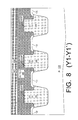
As shown in FIG. 8 (cross section Y1–Y1′), a conductive polysilicon layer 140 is formed over the structure by a conformal deposition process (e.g. low pressure chemical vapor deposition, “LPCVD”). Polysilicon 140 fills the spaces between the oxide protrusions 220P. The top polysilicon surface is planar because the polysilicon portions deposited on the sidewalls of protrusions 220P meet together.
Non-conformal deposition processes, whether known or to be invented, can also be used. If the top surface of polysilicon 140 is not planar, it is believed that the polysilicon 140 can be planarized after the deposition using known techniques (e.g. spinning a photoresist layer over the polysilicon 140 and then simultaneously etching the resist and the polysilicon at equal etch rates until all of the photoresist is removed). The bottom surface of polysilicon 140 is non-planar as it goes up and down over the oxide protrusions 220P.
An exemplary final thickness of polysilicon 140 is 0.06 μm over the active areas.
Silicon nitride 810 is deposited on polysilicon 140, by LPCVD for example, to an exemplary thickness of 1500 Å. If desired, a pad oxide layer (not shown) can be formed on polysilicon 140 before the nitride deposition. The pad oxide layer will provide an additional protection for the select gates during the etch of control gate polysilicon 170 described below in connection with FIG. 18.
In some embodiments, the top surface of polysilicon 140 and/or nitride 810 is not planar.
The wafer is coated with a photoresist layer (not shown). The resist is patterned to define select gate lines 140. See FIG. 2, and see also the perspective view in FIG. 9. Each select gate line 140 extends in the Y direction through the entire array. The memory array geometry is not sensitive to a misalignment between the mask defining the lines 140 and the mask defining the isolation trenches 220T (FIG. 4) except possibly at the boundary of the memory array.
Silicon nitride 810 is etched through the resist openings. The resist is removed, and polysilicon 140 is etched away where exposed by nitride 810. Select gate lines 140 are formed as a result. (In an alternative embodiment, the resist defining the nitride 810 is removed after the etch of polysilicon 140.)
As shown in FIG. 10 (cross section X–X′), the structure is oxidized to grow silicon dioxide 1010 on the sidewalls of select gate lines 140. Then a thin conformal silicon nitride layer 1030 is deposited and etched anisotropically, without a mask over the memory array, to form spacers on the sidewalls of each structure consisting of a select gate line 140, the overlying nitride 810, and the sidewall oxide 1010. Formation of silicon nitride spacers is described, for example, in U.S. Pat. No. 6,355,524 issued Mar. 12, 2002 to H. Tuan et al. and incorporated herein by reference.
A blanket oxide etch removes the exposed portions of silicon dioxide 130. Silicon dioxide 150 (FIG. 11, cross section X–X′) is thermally grown on substrate 120 to a desired thickness, e.g. 90 Å.
Floating gate polysilicon 160 is deposited over the structure, by LPCVD for example, and is doped during or after the deposition. Polysilicon 160 is sufficiently thick to ensure that the top surface of layer 160 is at least as high as the top surface of nitride 810. In particular, the top surface of polysilicon 160 includes regions 160T between the select gates 140. Regions 160T are at least as high as the top surface of nitride 810.
Layer 160 is planarized by a CMP process that stops on nitride 810, or by some other process. See FIG. 12 (cross section X–X′). The top surface of polysilicon 160 becomes coplanar with the top surface of nitride 810. CMP processes and slurries are known that allow one to avoid dishing in the top surface of the polysilicon layer.
Then polysilicon 160 is etched. Layer 160 is not masked in the memory array area. See FIGS. 13A (cross section X–X′) and 13B (cross section Y2–Y2′). The etch stops when trench oxide 220 becomes exposed. A suitable overetch is performed to completely remove the polysilicon 160 from the top surface of oxide 220. In some embodiments, the final thickness of layer 160 is 1200 Å.
Optionally, a timed etch of oxide 220 is performed to recess the top surface of oxide 220 below the surface of polysilicon 160. See FIG. 14 (cross section Y2–Y2′). This etch will improve the capacitive coupling between the floating and control gates. See the aforementioned U.S. Pat. No. 6,355,524. In the embodiment of FIG. 14, the oxide 220 continues to protrude above the top surface of substrate 120, as shown at 220P, by at least 0.10 μm. In other embodiments, the oxide 220 does not protrude above the substrate after the etch.
ONO layer 1510 (FIG. 15, cross section X–X′) is formed over the structure. For example, a silicon dioxide layer can be thermally grown on polysilicon 160 or deposited by a high temperature oxidation process (HTO) to a thickness of 50 Å. (HTO is described, for example, in U.S. patent application published as No. 2002/0197888 on Dec. 26, 2002, incorporated herein by reference). Then a silicon nitride layer can be deposited by LPCVD to a thickness of 80 Å. Then another silicon dioxide layer can be deposited by HTO to a thickness of 50 Å. These processes and thickness values are exemplary and not limiting.
Control gate polysilicon layer 170 (FIG. 16, cross section X–X′) is deposited on ONO 1510. Polysilicon 170 is doped N+ in the memory array area during or after the deposition.
The top surface of polysilicon 170 is not planar. Layer 170 has a protruding portion 170.1 over each select gate line 140. The protrusions 170.1 will be used to define the control and floating gates without additional dependence on photolithographic alignment.
As shown in FIG. 16, cavities 170C form in layer 170 between protrusions 170.1. As shown in FIG. 17 (cross section X–X′), these cavities are filled with some material 1710. In one embodiment, material 1710 is silicon dioxide deposited on polysilicon 170 and planarized by CMP or some other process. The memory array area has a planar top surface, with polysilicon 170 exposed.
Polysilicon 170 is etched without a mask selectively to oxide 1710. See FIG. 18 (cross section X–X′). This etch attacks the polysilicon portions 170.1 and creates cavities 1810 in the top surface of the structure. Polysilicon 170 is recessed relative to oxide 1710 in these cavities. In the embodiment of FIG. 18, this etch exposes ONO 1510, and continues for some time to recess the top surface of polysilicon 170 below the top surface of ONO 1510. This is not necessary however. The polysilicon etch can stop before exposing the ONO 1510, or the etch can stop when the ONO layer becomes exposed. If ONO 1510 is exposed, the width W1 of the polysilicon layer 170 in cavities 1810 on a side of select gate 140 will define the width of the control and floating gates in a self-aligned manner as will be illustrated below.
In some embodiments, the minimum thickness of polysilicon 170 (at the bottom of cavities 1810) is 0.18 μm, and the width W1 is also 0.18 μm. In FIG. 18, the top surface of polysilicon 170 is recessed in cavities 1810. In another embodiment, polysilicon 170 has a planar top surface throughout the memory array area.
A protective material is deposited into cavities 1810 to protect the polysilicon 170 portions near the select gates 140. In one embodiment, this material is silicon nitride 1910 (see FIG. 19, cross section X–X′). Nitride 1910 is deposited over the structure and polished by CMP until the oxide 1710 is exposed in the memory array area. See FIG. 20A (cross section X–X′). Nitride 1910 remains in cavities 1810.
Instead of CMP, the nitride 1910 can be processed by depositing a layer of material (not shown) having a planar top surface, and etching that material and the nitride with equal etch rates until the oxide 1710 is exposed. The material can be photoresist. The material can be removed after the nitride etch.
An antireflective coating layer (ARC) 2010, shown in FIG. 20A, is flowed on nitride 1910 and cured. The structure has a planar top surface after this step.
The wafer is coated with a photoresist layer 2020. The resist is patterned to protect the portion of nitride 1910 on one side of each select gate line 140. FIG. 20B (top view) illustrates the position of mask 2020 with respect to the features shown in FIG. 2. Resist 2020 overlies the future positions of control gate lines 170, and exposes those areas between the adjacent select gate lines 140 in which the control gate polysilicon 170 will be removed. The longitudinal edges of mask 2020 can be located anywhere over the select gate lines 140. The precise mask alignment is therefore not critical in the array area.
Silicon nitride 1910 and ARC 2010 are etched away where exposed by resist 2020. Resist 2020 and the remaining portions of ARC 2010 are then removed. The resulting memory array structure is shown in FIG. 21 (cross section X–X′). Nitride 1910 protects the polysilicon 170 portions of the width W1 (FIGS. 18, 21) at the bottom of cavities 1810.
Oxide 1710 is etched away by a blanket etch. The resulting structure is shown in FIG. 22 (cross section X–X′).
Polysilicon 170 is etched in the array area with nitride 1910 as a mask. The etch is selective to silicon dioxide, so the etch stops on ONO 1510. The resulting structure is shown in FIG. 23 (cross section X–X′).
ONO 1510 and polysilicon 160 are etched with nitride 1910 as a mask. Layers 1510, 160 are completely removed from the areas not covered by nitride 1910. See FIG. 24 (cross section X–X′). Nitride layers 1910, 810, 1030 can be partially removed during the etch of ONO 1510. Floating gates 160 and control gate lines 170 are fully defined at the conclusion of this step, and are as in FIGS. 2 and 3. The width of the top surface of control gate line 170 is W1, defined as described above in connection with FIG. 18.
The wafer is coated with photoresist 2620. The resist is patterned to expose the source lines 178 (FIG. 25A, cross section X–X′, and FIG. 25B, top view of the array without the dielectric layers). Each source line 178 traverses the memory array between two adjacent control gate lines 170, and provides one source/drain region to each cell in the two rows associated with the two control gate lines.
The alignment of mask 2620 is not critical because the left and right edges of the mask openings can be positioned anywhere over the respective select gate lines 140 or control gate lines 170.
Silicon dioxide 220 is etched out of trenches 220T in the areas exposed by mask 2620, i.e. the areas of source lines 178. This etch removes oxide 150 in the active areas over the source lines. Then the source line implant (N+) is performed using the same mask. In some embodiments, this is a high energy, high dose implant, possibly preceded by a lower energy, low dose, large angled implant (the angle can be 10° to 30° for example), to achieve a 0.1 μm to 0.2 μm source line diffusion depth.
In an alternative embodiment, mask 2620 is formed, then a high energy N+ implant is performed before etching out the oxide 220, then the oxide 220 is etched out of the trenches using the same mask, and then another, lower energy N type implant is performed using the same mask. The first (high energy) implant is at least partially blocked by oxide 220 in the trenches to avoid shorting the source lines 178 to N type isolation region 604 (FIG. 6). See the aforementioned U.S. Pat. No. 6,355,524.
Resist 2620 is removed. A thin silicon dioxide layer 2904 (FIG. 26A, cross section X–X′) is deposited over the structure by any suitable technique (e.g. TEOS, HTO, RTO). An exemplary thickness of oxide 2904 on the silicon surface of substrate 120 is 200 Å to 300 Å. If oxide 2904 is deposited thermally (e.g. by RTO, rapid thermal oxidation), the oxide will be much thinner on the silicon nitride surfaces.
A thin silicon nitride layer 2910 is deposited and etched anisotropically without a mask to form sidewall spacers on the gates of the peripheral transistors (not shown). Spacers 2910 also form in the memory array. Oxide 2904 serves as an etch stop protecting the substrate 120. An N+ implant is performed to create LDD (lightly doped drain) structures for the peripheral NMOS transistors (not shown), increase the dopant concentration in the peripheral NMOS transistor gates and in source line regions 178, and to dope bitline regions 174. FIG. 26B is a top view of the resulting memory array structure. The floating, control and select gates and the overlying nitride layers mask this implant so no additional masking in the array area is needed.
The memory fabrication can be completed using known techniques. In the example of FIG. 27, inter-level dielectric 3104 is deposited over the wafer. Contact openings are etched in dielectric layers 3104, 2904, 150 to expose the bitline regions 174. A conductive layer 3110 is deposited and patterned to form the bitlines that contact the bitline regions 174. If the layers 3104, 2904, 150 are formed from silicon oxide, the alignment of the mask (not shown) defining the contact openings is not critical because the select gates 140 are protected by nitride layers 2910, 1030.
FIG. 28 is a circuit diagram of one embodiment of the array. This is a NOR array, of the type described in the aforementioned U.S. Pat. No. 6,355,524. Each bitline 3110 is shared by two columns of the memory cells 3210. A cell 3210 is programmed by hot electron injection from the cell's channel region (the P type region in substrate 120 below the cell's floating and select gates) to floating gate 160. The cell is erased by Fowler-Nordheim tunneling of electrons from floating gate 160 to source line region 178 or the channel region.
Other details of the memory fabrication process are given in U.S. patent application Ser. No. 10/393,212, filed by Yi Ding on Mar. 19, 2003 and incorporated herein by reference.
The invention is not limited to such erase or programming techniques or to NOR memory arrays. The invention is not limited to the array architectures described above. For example, the source lines can be formed from a layer overlying the substrate 120 and contacting the source line substrate regions 178; the source lines do not have to go through the isolation trenches. Also, substrate isolation regions 220 do not have to traverse the entire array. In FIG. 29, the substrate isolation regions are interrupted at source lines 178. Dielectric 220 does not have to be etched out of the trenches before the source lines are doped. Shallow trench isolation can be replaced with LOCOS or other isolation types, known or to be invented. The invention is applicable to multi-level cell memories (the memories in which the cell may contain multiple bits of information).
The invention is not limited to memories. FIG. 30 illustrates a cross section of a semiconductor structure in the process of fabrication. This can be a non-memory structure. The structure includes a semiconductor substrate 120 and upward protrusions 140. Each protrusion 140 is shown as a feature formed on the top surface of substrate 120, but the features 140 can be part of substrate 120, or they can be made from layers made on top of other layers formed on substrate 120.
In a flash memory, each feature 140 can be a select gate, or a combination of a select gate and other layers (e.g. layers 1010, 1030, 810 of FIG. 10).
Self-aligned features are formed adjacent to protrusions 140 from a layer 160 (FIG. 31). Layer 160 is a combination of sub-layers 160.1, 160.2, 160.3, 160.4. Four sub-layers 160.1160.4 are shown, but any number of sub-layers 160.i (i=0, 1, . . . ) can be present, and each sub-layer in its turn may consist of multiple sub-layers. Different layers 160.i may be made of different materials. Each layer 160.i may or may not be patterned before other layers 160.i are deposited. In FIG. 31, layers 160.3, 160.4 overlie the protrusions 140, but the layers 160.1, 160.2 do not. Layer 160.1 may have been deposited over the structure and then etched off from over the features 140. Then layer 160.2 may have been deposited and etched in a similar manner. Then the layers 160.3, 160.4 were deposited. In other embodiments, all of the layers 160.i (i=1, 2, . . . ) overlie the protrusions 140. Also, the layers 160.i do not have to overlie each other. For example, layers 160.1, 160.2, 160.3 may all be exposed at the top surface of the structure.
Layer 160 of FIG. 31 may correspond to one or more of the layers 160, 1510, 170 in FIG. 17.
In FIG. 31, the top surface of layer 160 is not planar. Layer 160 has a protruding portion 170.1 over each feature 140. The protrusions 170.1 will be used to define the layer 160 in a self-aligned manner.
As shown in FIG. 31, cavities 170C form in layer 160 between protrusions 170.1. These cavities are filled with some layer 1710. In one embodiment, layer 1710 is silicon dioxide deposited on layer 160 and planarized by CMP or some other process. The structure has a planar top surface, with layer 160 exposed. In other embodiments, layer 1710 is photoresist, polyimide, or some other material. A non-planar top surface is also possible.
Layer 160 is etched selectively to layer 1710. See FIG. 32. No mask is needed. This etch creates cavities 1810 over the protrusions 140. Each cavity 1810 extends to the left and right of the respective protrusion 140. In FIG. 32, the etch terminates when the protrusions 140 become exposed. This is not necessary, however. The etch may terminate earlier, before the layer 160.3 is etched off the features 140. In other embodiments, the etch continues after the exposure of features 140, and the features 140 may or may not be attacked by the etch. In FIG. 32, the top surface of layer 160 is not planar after the etch. In other embodiments, the top surface of layer 160 is planar after the etch.
A protective layer 1910 (FIG. 33) is formed in cavities 1810 to protect the layer 160 near protrusions 140. Layer 1910 can be polyimide, photoresist, silicon nitride (as in FIG. 19), or any other suitable material. Layer 1910 may fill the cavities 1810 completely or partially (see FIG. 19). Layer 1910 may protrude upward from cavities 1810.
Layer 1710 is removed by a blanket etch selective to layer 1910. The resulting structure is shown in FIG. 34.
Layer 160 is etched with layer 1910 as a mask. The resulting structure is shown in FIG. 35. Self-aligned features are formed around protrusions 140. Each self-aligned feature includes portions of layers 160.1160.4.
The subsequent processing may include removal of layer 1910. Also, the layers 160.1160.4 may be removed from one side of each protrusion 140 using a mask. The alignment of this mask is not critical because the edges of the mask openings can be positioned anywhere over the respective protrusions 140 (cf. mask 2020 in FIG. 20). Alternatively, the removal of layers 160.1160.4 from one side of each protrusion can be performed before the complete removal of layer 1710, as in FIG. 20. The processing depends on the particular requirements. In some embodiments, the layers 160.1160.4 are left on all the side around protrusions 140.
The invention is not limited to any particular processing steps, materials, or other particulars. Other embodiments and variations are within the scope of the invention, as defined by the appended claims.

Claims (7)

1. A method for fabricating an integrated circuit, the method comprising:
(a) forming a structure comprising a semiconductor substrate, the structure comprising a first upward protruding feature;
(b) forming a first layer on the structure, the first layer having a first portion protruding upward over the first feature;
(c) forming a second layer over the first layer such that the first portion is exposed and not completely covered by the second layer;
(d) partially removing the first layer selectively to the second layer to form a cavity at the location of the first feature;
(e) forming a third layer in the cavity; and
(f) removing at least parts of the second layer and the first layer selectively to the third layer.
2. The method of claim 1 wherein the first layer comprises a plurality of sub-layers, and at least two sub-layers are made from different materials.
3. The method of claim 2 wherein the first portion comprises a portion of at least one sub-layer of the first layer, but the first portion does not comprise a portion of each sub-layer of the first layer.
4. The method of claim 2 wherein at least the bottom sub-layer of the first layer does not overlie the first feature, but at least the top sub-layer of the first layer overlies the first feature.
5. The method of claim 4 wherein the removing operation that removes the parts of the second and first layers does not completely remove any of the sub-layers of the first layer, each sub-layer having a portion covered by the third layer and remaining in the integrated circuit.
6. The method of claim 1 wherein forming the first layer comprises:
forming a first sub-layer of the first layer, and removing a portion of the first sub-layer over said feature; and then
forming a second sub-layer over the first sub-layer and over said feature.
7. The method of claim 6 wherein the second sub-layer comprises a layer L1 and a layer L2 overlying the layer L1; and
the partial removing of the first layer comprises partial removing of the layer L2 but not of the layer L1.
US10/393,202 2003-03-19 2003-03-19 Fabrication of integrated circuit elements in structures with protruding features Expired - Fee Related US6995060B2 (en)

Priority Applications (2)

Application Number Priority Date Filing Date Title
US10/393,202 US6995060B2 (en) 2003-03-19 2003-03-19 Fabrication of integrated circuit elements in structures with protruding features
TW093103312A TWI240353B (en) 2003-03-19 2004-02-12 Fabrication of integrated circuit elements in structures with protruding features

Applications Claiming Priority (1)

Application Number Priority Date Filing Date Title
US10/393,202 US6995060B2 (en) 2003-03-19 2003-03-19 Fabrication of integrated circuit elements in structures with protruding features

Publications (2)

Publication Number Publication Date
US20040185614A1 US20040185614A1 (en) 2004-09-23
US6995060B2 true US6995060B2 (en) 2006-02-07

Family

ID=32988088

Family Applications (1)

Application Number Title Priority Date Filing Date
US10/393,202 Expired - Fee Related US6995060B2 (en) 2003-03-19 2003-03-19 Fabrication of integrated circuit elements in structures with protruding features

Country Status (2)

Country Link
US (1) US6995060B2 (en)
TW (1) TWI240353B (en)

Cited By (3)

* Cited by examiner, † Cited by third party
Publication number Priority date Publication date Assignee Title
US20050224860A1 (en) * 2002-06-20 2005-10-13 Koninklijke Philips Electronics N.V. Conductive spacers extended floating gates
US20060003540A1 (en) * 2004-06-30 2006-01-05 Asml Netherlands B.V. Marker for alignment of non-transparent gate layer, method for manufacturing such a marker, and use of such a marker in a lithographic apparatus
US20090166704A1 (en) * 2007-12-26 2009-07-02 Masaaki Higashitani Non-volatile storage with substrate cut-out and process of fabricating

Families Citing this family (3)

* Cited by examiner, † Cited by third party
Publication number Priority date Publication date Assignee Title
US7709879B2 (en) * 2004-06-15 2010-05-04 Nxp B.V. Non-volatile memory with erase gate on isolation zones
US7342272B2 (en) * 2005-08-31 2008-03-11 Micron Technology, Inc. Flash memory with recessed floating gate
US9397176B2 (en) * 2014-07-30 2016-07-19 Freescale Semiconductor, Inc. Method of forming split gate memory with improved reliability

Citations (59)

* Cited by examiner, † Cited by third party
Publication number Priority date Publication date Assignee Title
US4701776A (en) 1983-08-29 1987-10-20 Seeq Technology, Inc. MOS floating gate memory cell and process for fabricating same
US5402371A (en) 1992-10-09 1995-03-28 Oki Electric Industry Co., Ltd. Method of writing data into and erasing the same from semiconductor nonvolatile memory
US5408115A (en) 1994-04-04 1995-04-18 Motorola Inc. Self-aligned, split-gate EEPROM device
US5424979A (en) 1992-10-02 1995-06-13 Matsushita Electric Industrial Co., Ltd. Non-volatile memory cell
US5445983A (en) 1994-10-11 1995-08-29 United Microelectronics Corporation Method of manufacturing EEPROM memory device with a select gate
US5633185A (en) 1992-01-22 1997-05-27 Macronix International Co., Ltd. Method of making a non-volatile memory cell
US5668757A (en) 1996-03-18 1997-09-16 Jeng; Ching-Shi Scalable flash eeprom memory cell and array
US5705415A (en) 1994-10-04 1998-01-06 Motorola, Inc. Process for forming an electrically programmable read-only memory cell
US5821143A (en) 1995-04-27 1998-10-13 Samsung Electronics Co., Ltd. Fabrication methods for nonvolatile memory devices including extended sidewall electrode
US5856943A (en) 1996-03-18 1999-01-05 Integrated Memory Technologies, Inc. Scalable flash EEPROM memory cell and array
US5901084A (en) 1997-03-10 1999-05-04 Mitsubishi Denki Kabushiki Kaisha Nonvolatile semiconductor memory device having floating gate electrode
US5910912A (en) 1992-10-30 1999-06-08 International Business Machines Corporation Flash EEPROM with dual-sidewall gate
US5912843A (en) 1996-03-18 1999-06-15 Integrated Memory Technologies, Inc. Scalable flash EEPROM memory cell, method of manufacturing and operation thereof
US5918124A (en) 1997-10-06 1999-06-29 Vanguard International Semiconductor Corporation Fabrication process for a novel multi-storage EEPROM cell
EP0938098A2 (en) 1998-02-18 1999-08-25 Nec Corporation Nonvolatile semiconductor memory device having a program area
US6011725A (en) 1997-08-01 2000-01-04 Saifun Semiconductors, Ltd. Two bit non-volatile electrically erasable and programmable semiconductor memory cell utilizing asymmetrical charge trapping
US6040216A (en) 1997-08-11 2000-03-21 Mosel Vitelic, Inc. Method (and device) for producing tunnel silicon oxynitride layer
US6057575A (en) 1996-03-18 2000-05-02 Integrated Memory Technologies, Inc. Scalable flash EEPROM memory cell, method of manufacturing and operation thereof
US6130129A (en) 1998-07-09 2000-10-10 Winbond Electronics Corp. Method of making self-aligned stacked gate flush memory with high control gate to floating gate coupling ratio
US6134144A (en) 1997-09-19 2000-10-17 Integrated Memory Technologies, Inc. Flash memory array
US6133098A (en) 1999-05-17 2000-10-17 Halo Lsi Design & Device Technology, Inc. Process for making and programming and operating a dual-bit multi-level ballistic flash memory
US6162682A (en) 1995-09-29 2000-12-19 Cypress Semiconductor Corporation Structure and process for a gouge-free stacked non-volatile memory cell with select gate
US6171909B1 (en) * 1999-03-01 2001-01-09 United Semiconductor Corp. Method for forming a stacked gate
US6187636B1 (en) 1997-03-14 2001-02-13 Hyundai Electronics Industries Co., Ltd. Flash memory device and fabrication method thereof
US6200856B1 (en) 1998-03-25 2001-03-13 Winbond Electronics Corporation Method of fabricating self-aligned stacked gate flash memory cell
US6214669B1 (en) 1996-07-30 2001-04-10 Nec Corporation Single-chip contact-less read-only memory (ROM) device and the method for fabricating the device
US6218689B1 (en) 1999-08-06 2001-04-17 Advanced Micro Devices, Inc. Method for providing a dopant level for polysilicon for flash memory devices
US6228695B1 (en) 1999-05-27 2001-05-08 Taiwan Semiconductor Manufacturing Company Method to fabricate split-gate with self-aligned source and self-aligned floating gate to control gate
US6232185B1 (en) 2000-05-15 2001-05-15 Integrated Memory Technologies, Inc. Method of making a floating gate memory cell
US6261856B1 (en) 1987-09-16 2001-07-17 Semiconductor Energy Laboratory Co., Ltd. Method and system of laser processing
US6266278B1 (en) 1999-06-30 2001-07-24 Sandisk Corporation Dual floating gate EEPROM cell array with steering gates shared adjacent cells
US6265739B1 (en) 1997-07-10 2001-07-24 Kabushiki Kaisha Toshiba Non-volatile semiconductor memory device and its manufacturing method
US6294297B1 (en) 1997-01-08 2001-09-25 Kabushiki Kaisha Toshiba Computer program product for calculating a process tolerance relating exposure amount and focal point position
US6326661B1 (en) 1999-07-29 2001-12-04 U.S. Philips Corporation Semiconductor device
US6355524B1 (en) 2000-08-15 2002-03-12 Mosel Vitelic, Inc. Nonvolatile memory structures and fabrication methods
US6365457B1 (en) 1998-03-26 2002-04-02 Samsung Electronics Co., Ltd. Method for manufacturing nonvolatile memory device using self-aligned source process
US6388293B1 (en) 1999-10-12 2002-05-14 Halo Lsi Design & Device Technology, Inc. Nonvolatile memory cell, operating method of the same and nonvolatile memory array
US20020064071A1 (en) 1997-12-10 2002-05-30 Matsushita Electronics Corporation Nonvolatile semiconductor memory device and method for driving the same
US6414872B1 (en) 2000-06-21 2002-07-02 National Semiconductor Corporation Compact non-volatile memory device and memory array
US6420231B1 (en) 1999-06-30 2002-07-16 Sandisk Corporation Processing techniques for making a dual floating gate EEPROM cell array
US6438036B2 (en) 1989-02-06 2002-08-20 Hitachi, Ltd. Nonvolatile semiconductor memory device
US6437360B1 (en) 1998-03-25 2002-08-20 Korea Advanced Institute Of Science And Technology Vacuum field transistor
US6436764B1 (en) 2000-06-08 2002-08-20 United Microelectronics Corp. Method for manufacturing a flash memory with split gate cells
US6468865B1 (en) 2000-11-28 2002-10-22 Advanced Micro Devices, Inc. Method of simultaneous formation of bitline isolation and periphery oxide
US6486023B1 (en) 1997-10-31 2002-11-26 Texas Instruments Incorporated Memory device with surface-channel peripheral transistor
US20020197888A1 (en) 2001-06-21 2002-12-26 Cheng-Chieh Huang Method of forming a silicon oxide layer
US6518618B1 (en) 1999-12-03 2003-02-11 Intel Corporation Integrated memory cell and method of fabrication
US6541829B2 (en) 1999-12-03 2003-04-01 Kabushiki Kaisha Toshiba Semiconductor device and method of manufacturing the same
US6541324B1 (en) 2001-11-02 2003-04-01 Silicon Storage Technology, Inc. Method of forming a semiconductor array of floating gate memory cells having strap regions and a peripheral logic device region
US6566196B1 (en) 2002-05-15 2003-05-20 Mosel Vitelic, Inc. Sidewall protection in fabrication of integrated circuits
US6635533B1 (en) 2003-03-27 2003-10-21 Powerchip Semiconductor Corp. Method of fabricating flash memory
US6642103B2 (en) 2000-03-08 2003-11-04 Koninklijke Philips Electronics N.V. Semiconductor device and method of manufacturing the same
US20030218908A1 (en) 2002-05-24 2003-11-27 Park Joo Weon Virtual ground nonvolatile semiconductor memory array architecture and integrated circuit structure therefor
US6660589B2 (en) 2001-12-19 2003-12-09 Samsung Electronics Co., Ltd. Semiconductor devices and methods for fabricating the same
US20040004863A1 (en) 2002-07-05 2004-01-08 Chih-Hsin Wang Nonvolatile electrically alterable memory device and array made thereby
US6696340B2 (en) 2001-01-11 2004-02-24 Seiko Epson Corporation Semiconductor devices having a non-volatile memory transistor and methods for manufacturing the same
US6747310B2 (en) 2002-10-07 2004-06-08 Actrans System Inc. Flash memory cells with separated self-aligned select and erase gates, and process of fabrication
US6764905B2 (en) 2001-11-06 2004-07-20 Integrated Memory Technologies, Inc. Method of manufacturing a scalable flash EEPROM memory cell with floating gate spacer wrapped by control gate
US6803276B2 (en) 2001-01-31 2004-10-12 Samsung Electronics Co., Ltd. Semiconductor device having a flash memory cell and fabrication method thereof

Patent Citations (62)

* Cited by examiner, † Cited by third party
Publication number Priority date Publication date Assignee Title
US4701776A (en) 1983-08-29 1987-10-20 Seeq Technology, Inc. MOS floating gate memory cell and process for fabricating same
US6261856B1 (en) 1987-09-16 2001-07-17 Semiconductor Energy Laboratory Co., Ltd. Method and system of laser processing
US6438036B2 (en) 1989-02-06 2002-08-20 Hitachi, Ltd. Nonvolatile semiconductor memory device
US5633185A (en) 1992-01-22 1997-05-27 Macronix International Co., Ltd. Method of making a non-volatile memory cell
US5424979A (en) 1992-10-02 1995-06-13 Matsushita Electric Industrial Co., Ltd. Non-volatile memory cell
US5402371A (en) 1992-10-09 1995-03-28 Oki Electric Industry Co., Ltd. Method of writing data into and erasing the same from semiconductor nonvolatile memory
US6107141A (en) 1992-10-30 2000-08-22 International Business Machines Corporation Flash EEPROM
US5910912A (en) 1992-10-30 1999-06-08 International Business Machines Corporation Flash EEPROM with dual-sidewall gate
US5408115A (en) 1994-04-04 1995-04-18 Motorola Inc. Self-aligned, split-gate EEPROM device
US5705415A (en) 1994-10-04 1998-01-06 Motorola, Inc. Process for forming an electrically programmable read-only memory cell
US5445983A (en) 1994-10-11 1995-08-29 United Microelectronics Corporation Method of manufacturing EEPROM memory device with a select gate
US5821143A (en) 1995-04-27 1998-10-13 Samsung Electronics Co., Ltd. Fabrication methods for nonvolatile memory devices including extended sidewall electrode
US6162682A (en) 1995-09-29 2000-12-19 Cypress Semiconductor Corporation Structure and process for a gouge-free stacked non-volatile memory cell with select gate
US5856943A (en) 1996-03-18 1999-01-05 Integrated Memory Technologies, Inc. Scalable flash EEPROM memory cell and array
US6057575A (en) 1996-03-18 2000-05-02 Integrated Memory Technologies, Inc. Scalable flash EEPROM memory cell, method of manufacturing and operation thereof
US5668757A (en) 1996-03-18 1997-09-16 Jeng; Ching-Shi Scalable flash eeprom memory cell and array
US5912843A (en) 1996-03-18 1999-06-15 Integrated Memory Technologies, Inc. Scalable flash EEPROM memory cell, method of manufacturing and operation thereof
US6214669B1 (en) 1996-07-30 2001-04-10 Nec Corporation Single-chip contact-less read-only memory (ROM) device and the method for fabricating the device
US6294297B1 (en) 1997-01-08 2001-09-25 Kabushiki Kaisha Toshiba Computer program product for calculating a process tolerance relating exposure amount and focal point position
US5901084A (en) 1997-03-10 1999-05-04 Mitsubishi Denki Kabushiki Kaisha Nonvolatile semiconductor memory device having floating gate electrode
US6187636B1 (en) 1997-03-14 2001-02-13 Hyundai Electronics Industries Co., Ltd. Flash memory device and fabrication method thereof
US6265739B1 (en) 1997-07-10 2001-07-24 Kabushiki Kaisha Toshiba Non-volatile semiconductor memory device and its manufacturing method
US20030205776A1 (en) 1997-07-10 2003-11-06 Kabushiki Kaisha Toshiba Non-volatile semiconductor memory device and its manufacturing method
US6011725A (en) 1997-08-01 2000-01-04 Saifun Semiconductors, Ltd. Two bit non-volatile electrically erasable and programmable semiconductor memory cell utilizing asymmetrical charge trapping
US6040216A (en) 1997-08-11 2000-03-21 Mosel Vitelic, Inc. Method (and device) for producing tunnel silicon oxynitride layer
US6134144A (en) 1997-09-19 2000-10-17 Integrated Memory Technologies, Inc. Flash memory array
US5918124A (en) 1997-10-06 1999-06-29 Vanguard International Semiconductor Corporation Fabrication process for a novel multi-storage EEPROM cell
US6486023B1 (en) 1997-10-31 2002-11-26 Texas Instruments Incorporated Memory device with surface-channel peripheral transistor
US20020064071A1 (en) 1997-12-10 2002-05-30 Matsushita Electronics Corporation Nonvolatile semiconductor memory device and method for driving the same
EP0938098A2 (en) 1998-02-18 1999-08-25 Nec Corporation Nonvolatile semiconductor memory device having a program area
US6200856B1 (en) 1998-03-25 2001-03-13 Winbond Electronics Corporation Method of fabricating self-aligned stacked gate flash memory cell
US6437360B1 (en) 1998-03-25 2002-08-20 Korea Advanced Institute Of Science And Technology Vacuum field transistor
US6365457B1 (en) 1998-03-26 2002-04-02 Samsung Electronics Co., Ltd. Method for manufacturing nonvolatile memory device using self-aligned source process
US6130129A (en) 1998-07-09 2000-10-10 Winbond Electronics Corp. Method of making self-aligned stacked gate flush memory with high control gate to floating gate coupling ratio
US6171909B1 (en) * 1999-03-01 2001-01-09 United Semiconductor Corp. Method for forming a stacked gate
US6133098A (en) 1999-05-17 2000-10-17 Halo Lsi Design & Device Technology, Inc. Process for making and programming and operating a dual-bit multi-level ballistic flash memory
US6228695B1 (en) 1999-05-27 2001-05-08 Taiwan Semiconductor Manufacturing Company Method to fabricate split-gate with self-aligned source and self-aligned floating gate to control gate
US6266278B1 (en) 1999-06-30 2001-07-24 Sandisk Corporation Dual floating gate EEPROM cell array with steering gates shared adjacent cells
US6344993B1 (en) 1999-06-30 2002-02-05 Sandisk Corporation Dual floating gate EEPROM cell array with steering gates shared by adjacent cells
US6420231B1 (en) 1999-06-30 2002-07-16 Sandisk Corporation Processing techniques for making a dual floating gate EEPROM cell array
US6326661B1 (en) 1999-07-29 2001-12-04 U.S. Philips Corporation Semiconductor device
US6218689B1 (en) 1999-08-06 2001-04-17 Advanced Micro Devices, Inc. Method for providing a dopant level for polysilicon for flash memory devices
US6388293B1 (en) 1999-10-12 2002-05-14 Halo Lsi Design & Device Technology, Inc. Nonvolatile memory cell, operating method of the same and nonvolatile memory array
US6518618B1 (en) 1999-12-03 2003-02-11 Intel Corporation Integrated memory cell and method of fabrication
US6541829B2 (en) 1999-12-03 2003-04-01 Kabushiki Kaisha Toshiba Semiconductor device and method of manufacturing the same
US6642103B2 (en) 2000-03-08 2003-11-04 Koninklijke Philips Electronics N.V. Semiconductor device and method of manufacturing the same
US6232185B1 (en) 2000-05-15 2001-05-15 Integrated Memory Technologies, Inc. Method of making a floating gate memory cell
US6436764B1 (en) 2000-06-08 2002-08-20 United Microelectronics Corp. Method for manufacturing a flash memory with split gate cells
US6414872B1 (en) 2000-06-21 2002-07-02 National Semiconductor Corporation Compact non-volatile memory device and memory array
US6355524B1 (en) 2000-08-15 2002-03-12 Mosel Vitelic, Inc. Nonvolatile memory structures and fabrication methods
US6468865B1 (en) 2000-11-28 2002-10-22 Advanced Micro Devices, Inc. Method of simultaneous formation of bitline isolation and periphery oxide
US6696340B2 (en) 2001-01-11 2004-02-24 Seiko Epson Corporation Semiconductor devices having a non-volatile memory transistor and methods for manufacturing the same
US6803276B2 (en) 2001-01-31 2004-10-12 Samsung Electronics Co., Ltd. Semiconductor device having a flash memory cell and fabrication method thereof
US20020197888A1 (en) 2001-06-21 2002-12-26 Cheng-Chieh Huang Method of forming a silicon oxide layer
US6541324B1 (en) 2001-11-02 2003-04-01 Silicon Storage Technology, Inc. Method of forming a semiconductor array of floating gate memory cells having strap regions and a peripheral logic device region
US6764905B2 (en) 2001-11-06 2004-07-20 Integrated Memory Technologies, Inc. Method of manufacturing a scalable flash EEPROM memory cell with floating gate spacer wrapped by control gate
US6660589B2 (en) 2001-12-19 2003-12-09 Samsung Electronics Co., Ltd. Semiconductor devices and methods for fabricating the same
US6566196B1 (en) 2002-05-15 2003-05-20 Mosel Vitelic, Inc. Sidewall protection in fabrication of integrated circuits
US20030218908A1 (en) 2002-05-24 2003-11-27 Park Joo Weon Virtual ground nonvolatile semiconductor memory array architecture and integrated circuit structure therefor
US20040004863A1 (en) 2002-07-05 2004-01-08 Chih-Hsin Wang Nonvolatile electrically alterable memory device and array made thereby
US6747310B2 (en) 2002-10-07 2004-06-08 Actrans System Inc. Flash memory cells with separated self-aligned select and erase gates, and process of fabrication
US6635533B1 (en) 2003-03-27 2003-10-21 Powerchip Semiconductor Corp. Method of fabricating flash memory

Non-Patent Citations (28)

* Cited by examiner, † Cited by third party
Title
Bergemont, A. et al. "NOR Virtual Ground (NVG)- A New Scaling Concept for Very High Density FLAS EEPROM and its Implementation in a 0.5 um Process," 1993 IEEE 2.2.1-2.2.4.
Kim, K.S. et al. "A Novel Dual String NOR (DuSnor) Memory Cell Technology Scalable to the 256 Mbit and 1 Gbit Flash Memories," 1995 IEEE 11.1.1-11.1.4.
Ma, Y.; Pang, C.S.; Pathak, J.; Tsao, S.C.; Chang, C.F.; Yamauchi, Y.; Yoshimi, M. "A Novel High Density Contactless Flash Memory Array Using Split-Gate Source-Side-Injection Cell for 5V-Only Applications," 1994 Symposium on VLSI Technology Digest of Technical Papers, pp. 49-50.
Ma, Yale et al., "A Dual-Bit Split-Gate EEPROM (DS'G) Cell in Contactless Array for Single Vcc High Density Flash Memories," 1994 IEEE, 3.5.1-3.5.4.
Mih, Rebecca et al. "0.18um Modular Triple Self-Aligned Embedded Split-Gate Flash Memory," 2000 Symposium on VLSI Technology Digest of Technical Papers, pp. 120-121.
Mizutani, Yoshihisa; and Makita, Koji "A New EPROM Cell With A Sidewall Floating Gate Fro High-Density and High Performance Device," 1985 IEEE, 635-638.
Naruke, K.; Yamada, S.; Obi, E.; Taguchi, S.; and Wada, M. "A New Flash-Erase EEPROM Cell with A Sidewall Select-Gate On Its Source Side," 1989 IEEE, pp. 604-606.
Shirota, Riichiro "A Review of 256Mbit NAND Flash Memories and NAND Flash Future Trend," Feb. 2000, Nonvolatile Memory Workshop in Monterey, California, pp. 22-31.
Spinelli, Alessandro S., "Quantum-Mechanical 2D Simulation of Surface-and Buried-Channel p-MOS," 2000 International Conference on Simulation of Semiconductor Processes and Devices: SISPAD 2000, Seattle, WA Sep. 6-8, 2000.
U.S. Appl. No. 10/393,212, entitled "Nonvolatile Memories And Methods Of Fabrication," Filed on Mar. 19, 2003.
U.S. Appl. No. 10/393,212, filed on Mar. 19, 2003 entitled "Nonvolatile Memories And Methods of Fabrication,".
U.S. Appl. No. 10/411,813, entitled "Nonvolatile Memories With A Floating Gate Having An Upward Protrusion," Filed on Apr. 10, 2003.
U.S. Appl. No. 10/411,813, filed on Apr. 10, 2003, entitled "Nonvolatile Memories With A Floating Gate Having an Upward Protrusion,".
U.S. Appl. No. 10/440,005, entitled "Fabrication of Dielectric On A Gate Surface To Insulate The Gate From Another Element Of An Integrated Circuit," Filed on May 16, 2003.
U.S. Appl. No. 10/440,466, entitled "Fabrication Of Conductive Gates For Nonvolatile Memories From Layers With Protruding Portions," Filed on May 16, 2003.
U.S. Appl. No. 10/440,500, entitled "Integrated Circuits With Openings that Allow Electrical Contact To Conductive Features Having Self-Aligned Edges," Filed on May 16, 2003.
U.S. Appl. No. 10/440,508, entitled "Fabrication of Gate Dielectric In Nonvolatile Memories Having Select, Floating And Control Gates," Filed on May 16, 2003.
U.S. Appl. No. 10/631,452, entitled "Fabrication Of Dielectric For A Nonvolatile Memory Cell Having Multiple Floating Gates," Filed on Jul. 30, 2003.
U.S. Appl. No. 10/631,552, entitled "Nonvolatile Memories And Methods Of Fabrication," Filed on Jul. 30, 2003.
U.S. Appl. No. 10/631,941, entitled "Nonvolatile Memory Cell With Multiple Floating Gates Formed After The Select Gate," Filed on Jul. 30, 2003.
U.S. Appl. No. 10/632,007, entitled "Arrays Of Nonovolatile Memory Cells Wherein Each Cell Has Two Conductive Floating Gates," Filed on Jul. 30, 2003.
U.S. Appl. No. 10/632,154, entitled "Fabrication Of Gate Dielectric In Nonvolatile Memories In Which A Memory Cell Has Multiple Floating Gates," Filed on Jul. 30, 2003.
U.S. Appl. No. 10/632,155, entitled "Nonvolatile Memory Cells With Buried Channel Transistors," Filed on Jul. 30, 2004.
U.S. Appl. No. 10/632,186, entitled "Nonvolatile Memory Cell With Multiple Floating Gates Formed After The Select Gate and Having Upward Protrusions," Filed on Jul. 30, 2003.
U.S. Appl. No. 10/797,972, entitled "Fabrication of Conductive Lines Interconnecting First Conductive Gates in Nonvolatile Memories Having Second Conductive Gates Provided By Conductive Gates Lines, Wherein The Adjacent Conductive Gate Lines For The Adjacent Columns Are Spaced From Each Other, And Non-Volatile Memory Structures," Filed on Mar. 10, 2004.
U.S. Appl. No. 10/798,475, entitled "Fabrication of Conductive Lines Interconnecting Conductive Gates in Nonvolatile Memories and Non-Volatile Memory Structures," Filed on Mar. 10, 2004.
Van Duuren, Michiel et al., "Compact poly-CMP Embedded Flash Memory Cells For One or Two Bit Storage," Philips Research Leuven, Kapeldreef 75, B3001 Leuven, Belgium, pp. 73-74.
Wu, A.T.; Chan T.Y.; Ko, P.K.; and Hu, C. "A Novel High-Speed, 5-Volt Programming EPROM Structure With Source-Side Injection," 1986 IEEE, 584-587.

Cited By (12)

* Cited by examiner, † Cited by third party
Publication number Priority date Publication date Assignee Title
US20050224860A1 (en) * 2002-06-20 2005-10-13 Koninklijke Philips Electronics N.V. Conductive spacers extended floating gates
US7416939B2 (en) * 2002-06-20 2008-08-26 Nxp B.V. Conductive spacers extended floating gates
US20090087976A1 (en) * 2002-06-20 2009-04-02 Antonius Maria Petrus Hendriks Conductive Spacers Extended Floating Gates
US8278202B2 (en) 2002-06-20 2012-10-02 Nxp B.V. Conductive spacers extended floating gates
US20060003540A1 (en) * 2004-06-30 2006-01-05 Asml Netherlands B.V. Marker for alignment of non-transparent gate layer, method for manufacturing such a marker, and use of such a marker in a lithographic apparatus
US7271073B2 (en) * 2004-06-30 2007-09-18 Asml Nertherlands B.V. Marker for alignment of non-transparent gate layer, method for manufacturing such a marker, and use of such a marker in a lithographic apparatus
US20070284697A1 (en) * 2004-06-30 2007-12-13 Asml Netherlands B.V. Marker for alignment of non-transparent gate layer, method for manufacturing such a marker, and use of such a marker in a lithographic apparatus
US7453161B2 (en) 2004-06-30 2008-11-18 Asml Netherlands B.V. Marker for alignment of non-transparent gate layer, method for manufacturing such a marker, and use of such a marker in a lithographic apparatus
US20090166704A1 (en) * 2007-12-26 2009-07-02 Masaaki Higashitani Non-volatile storage with substrate cut-out and process of fabricating
US7923767B2 (en) 2007-12-26 2011-04-12 Sandisk Corporation Non-volatile storage with substrate cut-out and process of fabricating
US20110159649A1 (en) * 2007-12-26 2011-06-30 Masaaki Higashitani Non-volatile storage with substrate cut-out and process of fabricating
US8551839B2 (en) 2007-12-26 2013-10-08 Sandisk Technologies Inc. Non-volatile storage with substrate cut-out and process of fabricating

Also Published As

Publication number Publication date
TWI240353B (en) 2005-09-21
US20040185614A1 (en) 2004-09-23
TW200419698A (en) 2004-10-01

Similar Documents

Publication Publication Date Title
US7301196B2 (en) Nonvolatile memories and methods of fabrication
US6709922B2 (en) Method of manufacturing semiconductor integrated circuit device including nonvolatile semiconductor memory devices
US7018895B2 (en) Nonvolatile memory cell with multiple floating gates formed after the select gate
US6117733A (en) Poly tip formation and self-align source process for split-gate flash cell
KR100375235B1 (en) Sonos flash memory device and a method for fabricating the same
US6885044B2 (en) Arrays of nonvolatile memory cells wherein each cell has two conductive floating gates
US7091091B2 (en) Nonvolatile memory fabrication methods in which a dielectric layer underlying a floating gate layer is spaced from an edge of an isolation trench and/or an edge of the floating gate layer
US6271087B1 (en) Method for forming self-aligned contacts and local interconnects using self-aligned local interconnects
US6562681B2 (en) Nonvolatile memories with floating gate spacers, and methods of fabrication
US20060216891A1 (en) Non-volatile memory device and method of fabricating the same
US7238575B2 (en) Fabrication of conductive lines interconnecting conductive gates in nonvolatile memories, and non-volatile memory structures
US6893921B2 (en) Nonvolatile memories with a floating gate having an upward protrusion
US8952536B2 (en) Semiconductor device and method of fabrication
US7052947B2 (en) Fabrication of gate dielectric in nonvolatile memories in which a memory cell has multiple floating gates
US6897115B2 (en) Method of fabricating non-volatile memory device
US6482699B1 (en) Method for forming self-aligned contacts and local interconnects using decoupled local interconnect process
US7148104B2 (en) Fabrication of conductive lines interconnecting first conductive gates in nonvolatile memories having second conductive gates provided by conductive gate lines, wherein the adjacent conductive gate lines for the adjacent columns are spaced from each other, and non-volatile memory structures
US6962852B2 (en) Nonvolatile memories and methods of fabrication
US6995060B2 (en) Fabrication of integrated circuit elements in structures with protruding features
WO2005027194A2 (en) Method of making nonvolatile transistor pairs with shared control gate
US7008849B2 (en) Method for providing bitline contacts in a memory cell array and a memory cell array having bitline contacts
US7060565B2 (en) Fabrication of dielectric for a nonvolatile memory cell having multiple floating gates
US20070138538A1 (en) Method of forming self-aligned floating gate array and flash memory device including self-aligned floating gate array
JP2005051244A (en) Method for manufacturing integrated circuit
US7071115B2 (en) Use of multiple etching steps to reduce lateral etch undercut

Legal Events

Date Code Title Description
AS Assignment

Owner name: MOSEL VITELIC, INC., TAIWAN

Free format text: ASSIGNMENT OF ASSIGNORS INTEREST;ASSIGNOR:DING, YI;REEL/FRAME:013896/0026

Effective date: 20030318

AS Assignment

Owner name: PROMOS TECHNOLOGIES INC., TAIWAN

Free format text: ASSIGNMENT OF ASSIGNORS INTEREST;ASSIGNOR:MOSEL VITELIC, INC.;REEL/FRAME:015483/0947

Effective date: 20040622

REMI Maintenance fee reminder mailed
LAPS Lapse for failure to pay maintenance fees
STCH Information on status: patent discontinuation

Free format text: PATENT EXPIRED DUE TO NONPAYMENT OF MAINTENANCE FEES UNDER 37 CFR 1.362

FP Lapsed due to failure to pay maintenance fee

Effective date: 20100207