US6982230B2 - Deposition of hafnium oxide and/or zirconium oxide and fabrication of passivated electronic structures - Google Patents
Deposition of hafnium oxide and/or zirconium oxide and fabrication of passivated electronic structures Download PDFInfo
- Publication number
- US6982230B2 US6982230B2 US10/291,334 US29133402A US6982230B2 US 6982230 B2 US6982230 B2 US 6982230B2 US 29133402 A US29133402 A US 29133402A US 6982230 B2 US6982230 B2 US 6982230B2
- Authority
- US
- United States
- Prior art keywords
- hafnium
- zirconium
- liquid
- precursor
- oxide
- Prior art date
- Legal status (The legal status is an assumption and is not a legal conclusion. Google has not performed a legal analysis and makes no representation as to the accuracy of the status listed.)
- Expired - Fee Related
Links
- 229910000449 hafnium oxide Inorganic materials 0.000 title claims abstract description 106
- RVTZCBVAJQQJTK-UHFFFAOYSA-N oxygen(2-);zirconium(4+) Chemical compound [O-2].[O-2].[Zr+4] RVTZCBVAJQQJTK-UHFFFAOYSA-N 0.000 title claims abstract description 64
- 229910001928 zirconium oxide Inorganic materials 0.000 title claims abstract description 64
- 230000008021 deposition Effects 0.000 title claims description 23
- WIHZLLGSGQNAGK-UHFFFAOYSA-N hafnium(4+);oxygen(2-) Chemical group [O-2].[O-2].[Hf+4] WIHZLLGSGQNAGK-UHFFFAOYSA-N 0.000 title abstract description 65
- 238000004519 manufacturing process Methods 0.000 title abstract description 24
- 238000000034 method Methods 0.000 claims abstract description 64
- 239000007788 liquid Substances 0.000 claims abstract description 48
- 239000000203 mixture Substances 0.000 claims abstract description 42
- 238000000151 deposition Methods 0.000 claims abstract description 33
- 150000004703 alkoxides Chemical class 0.000 claims abstract description 24
- 239000007789 gas Substances 0.000 claims abstract description 17
- 230000008016 vaporization Effects 0.000 claims abstract description 11
- UFHFLCQGNIYNRP-UHFFFAOYSA-N Hydrogen Chemical compound [H][H] UFHFLCQGNIYNRP-UHFFFAOYSA-N 0.000 claims abstract description 8
- 239000001257 hydrogen Substances 0.000 claims abstract description 8
- 229910052739 hydrogen Inorganic materials 0.000 claims abstract description 8
- 239000002243 precursor Substances 0.000 claims description 61
- 229910052735 hafnium Inorganic materials 0.000 claims description 58
- 239000000758 substrate Substances 0.000 claims description 54
- VBJZVLUMGGDVMO-UHFFFAOYSA-N hafnium atom Chemical compound [Hf] VBJZVLUMGGDVMO-UHFFFAOYSA-N 0.000 claims description 48
- -1 zirconium alkoxide Chemical class 0.000 claims description 30
- 229910052751 metal Inorganic materials 0.000 claims description 26
- 239000002184 metal Substances 0.000 claims description 26
- 229910044991 metal oxide Inorganic materials 0.000 claims description 24
- 150000004706 metal oxides Chemical class 0.000 claims description 22
- 229910052726 zirconium Inorganic materials 0.000 claims description 19
- QVGXLLKOCUKJST-UHFFFAOYSA-N atomic oxygen Chemical compound [O] QVGXLLKOCUKJST-UHFFFAOYSA-N 0.000 claims description 14
- 229910052760 oxygen Inorganic materials 0.000 claims description 14
- 239000001301 oxygen Substances 0.000 claims description 14
- 239000000376 reactant Substances 0.000 claims description 8
- 239000004065 semiconductor Substances 0.000 claims description 7
- XLYOFNOQVPJJNP-UHFFFAOYSA-N water Substances O XLYOFNOQVPJJNP-UHFFFAOYSA-N 0.000 claims description 5
- CBENFWSGALASAD-UHFFFAOYSA-N Ozone Chemical compound [O-][O+]=O CBENFWSGALASAD-UHFFFAOYSA-N 0.000 claims description 4
- 239000002253 acid Substances 0.000 claims description 4
- 239000011229 interlayer Substances 0.000 claims description 4
- VIHLAKDKGTYILV-UHFFFAOYSA-N 2-methylpropan-1-ol zirconium Chemical compound [Zr].CC(C)CO.CC(C)CO.CC(C)CO.CC(C)CO VIHLAKDKGTYILV-UHFFFAOYSA-N 0.000 claims description 3
- BGGIUGXMWNKMCP-UHFFFAOYSA-N 2-methylpropan-2-olate;zirconium(4+) Chemical compound CC(C)(C)O[Zr](OC(C)(C)C)(OC(C)(C)C)OC(C)(C)C BGGIUGXMWNKMCP-UHFFFAOYSA-N 0.000 claims description 3
- 238000005033 Fourier transform infrared spectroscopy Methods 0.000 claims description 3
- 150000001412 amines Chemical class 0.000 claims description 3
- BSDOQSMQCZQLDV-UHFFFAOYSA-N butan-1-olate;zirconium(4+) Chemical compound [Zr+4].CCCC[O-].CCCC[O-].CCCC[O-].CCCC[O-] BSDOQSMQCZQLDV-UHFFFAOYSA-N 0.000 claims description 3
- FFOWIEZZYLIBTD-UHFFFAOYSA-N butan-2-olate zirconium(4+) Chemical compound CCC(C)O[Zr](OC(C)CC)(OC(C)CC)OC(C)CC FFOWIEZZYLIBTD-UHFFFAOYSA-N 0.000 claims description 3
- 239000000470 constituent Substances 0.000 claims description 3
- UARGAUQGVANXCB-UHFFFAOYSA-N ethanol;zirconium Chemical compound [Zr].CCO.CCO.CCO.CCO UARGAUQGVANXCB-UHFFFAOYSA-N 0.000 claims description 3
- 229930195733 hydrocarbon Natural products 0.000 claims description 3
- 150000002430 hydrocarbons Chemical class 0.000 claims description 3
- IKGXNCHYONXJSM-UHFFFAOYSA-N methanolate;zirconium(4+) Chemical compound [Zr+4].[O-]C.[O-]C.[O-]C.[O-]C IKGXNCHYONXJSM-UHFFFAOYSA-N 0.000 claims description 3
- XPGAWFIWCWKDDL-UHFFFAOYSA-N propan-1-olate;zirconium(4+) Chemical compound [Zr+4].CCC[O-].CCC[O-].CCC[O-].CCC[O-] XPGAWFIWCWKDDL-UHFFFAOYSA-N 0.000 claims description 3
- DJIFSIBYHXVGSS-UHFFFAOYSA-J zirconium(4+);tetraphenoxide Chemical compound [Zr+4].[O-]C1=CC=CC=C1.[O-]C1=CC=CC=C1.[O-]C1=CC=CC=C1.[O-]C1=CC=CC=C1 DJIFSIBYHXVGSS-UHFFFAOYSA-J 0.000 claims description 3
- QCWXUUIWCKQGHC-UHFFFAOYSA-N Zirconium Chemical compound [Zr] QCWXUUIWCKQGHC-UHFFFAOYSA-N 0.000 claims description 2
- 150000001299 aldehydes Chemical class 0.000 claims description 2
- 150000001338 aliphatic hydrocarbons Chemical class 0.000 claims description 2
- 125000000217 alkyl group Chemical group 0.000 claims description 2
- 150000004945 aromatic hydrocarbons Chemical class 0.000 claims description 2
- 150000002148 esters Chemical class 0.000 claims description 2
- 239000012948 isocyanate Substances 0.000 claims description 2
- 150000002513 isocyanates Chemical class 0.000 claims description 2
- 150000002576 ketones Chemical class 0.000 claims description 2
- 125000004971 nitroalkyl group Chemical group 0.000 claims description 2
- 238000009832 plasma treatment Methods 0.000 claims description 2
- 229920002545 silicone oil Polymers 0.000 claims description 2
- 150000003568 thioethers Chemical class 0.000 claims description 2
- RTZKZFJDLAIYFH-UHFFFAOYSA-N Diethyl ether Chemical compound CCOCC RTZKZFJDLAIYFH-UHFFFAOYSA-N 0.000 claims 2
- 239000004215 Carbon black (E152) Substances 0.000 claims 1
- LFQSCWFLJHTTHZ-UHFFFAOYSA-N Ethanol Chemical compound CCO LFQSCWFLJHTTHZ-UHFFFAOYSA-N 0.000 claims 1
- ISWSIDIOOBJBQZ-UHFFFAOYSA-N Phenol Chemical compound OC1=CC=CC=C1 ISWSIDIOOBJBQZ-UHFFFAOYSA-N 0.000 claims 1
- ZMZDMBWJUHKJPS-UHFFFAOYSA-M Thiocyanate anion Chemical compound [S-]C#N ZMZDMBWJUHKJPS-UHFFFAOYSA-M 0.000 claims 1
- 150000003973 alkyl amines Chemical class 0.000 claims 1
- XLJMAIOERFSOGZ-UHFFFAOYSA-M cyanate Chemical compound [O-]C#N XLJMAIOERFSOGZ-UHFFFAOYSA-M 0.000 claims 1
- 150000008282 halocarbons Chemical class 0.000 claims 1
- ZMZDMBWJUHKJPS-UHFFFAOYSA-N hydrogen thiocyanate Natural products SC#N ZMZDMBWJUHKJPS-UHFFFAOYSA-N 0.000 claims 1
- 125000001997 phenyl group Chemical group [H]C1=C([H])C([H])=C(*)C([H])=C1[H] 0.000 claims 1
- 238000002161 passivation Methods 0.000 abstract description 16
- 239000010410 layer Substances 0.000 description 68
- VYPSYNLAJGMNEJ-UHFFFAOYSA-N Silicium dioxide Chemical compound O=[Si]=O VYPSYNLAJGMNEJ-UHFFFAOYSA-N 0.000 description 66
- 239000010408 film Substances 0.000 description 59
- 239000003990 capacitor Substances 0.000 description 47
- 229910052681 coesite Inorganic materials 0.000 description 32
- 229910052906 cristobalite Inorganic materials 0.000 description 32
- 239000000377 silicon dioxide Substances 0.000 description 32
- 229910052682 stishovite Inorganic materials 0.000 description 32
- 229910052905 tridymite Inorganic materials 0.000 description 32
- 238000005229 chemical vapour deposition Methods 0.000 description 27
- 239000003989 dielectric material Substances 0.000 description 26
- 229910052710 silicon Inorganic materials 0.000 description 19
- XUIMIQQOPSSXEZ-UHFFFAOYSA-N Silicon Chemical compound [Si] XUIMIQQOPSSXEZ-UHFFFAOYSA-N 0.000 description 18
- 239000010703 silicon Substances 0.000 description 18
- 230000004888 barrier function Effects 0.000 description 17
- 229910021420 polycrystalline silicon Inorganic materials 0.000 description 15
- 229920005591 polysilicon Polymers 0.000 description 14
- 239000006200 vaporizer Substances 0.000 description 14
- 239000004020 conductor Substances 0.000 description 13
- 239000000463 material Substances 0.000 description 13
- IJGRMHOSHXDMSA-UHFFFAOYSA-N Atomic nitrogen Chemical compound N#N IJGRMHOSHXDMSA-UHFFFAOYSA-N 0.000 description 12
- 229910020286 SiOxNy Inorganic materials 0.000 description 12
- 229910004200 TaSiN Inorganic materials 0.000 description 12
- 229910045601 alloy Inorganic materials 0.000 description 12
- 239000000956 alloy Substances 0.000 description 12
- GWEVSGVZZGPLCZ-UHFFFAOYSA-N Titan oxide Chemical compound O=[Ti]=O GWEVSGVZZGPLCZ-UHFFFAOYSA-N 0.000 description 10
- PNEYBMLMFCGWSK-UHFFFAOYSA-N aluminium oxide Inorganic materials [O-2].[O-2].[O-2].[Al+3].[Al+3] PNEYBMLMFCGWSK-UHFFFAOYSA-N 0.000 description 10
- 229910052593 corundum Inorganic materials 0.000 description 10
- 230000008569 process Effects 0.000 description 10
- WOCIAKWEIIZHES-UHFFFAOYSA-N ruthenium(iv) oxide Chemical compound O=[Ru]=O WOCIAKWEIIZHES-UHFFFAOYSA-N 0.000 description 10
- 229910001845 yogo sapphire Inorganic materials 0.000 description 10
- 230000001603 reducing effect Effects 0.000 description 9
- BPQQTUXANYXVAA-UHFFFAOYSA-N Orthosilicate Chemical compound [O-][Si]([O-])([O-])[O-] BPQQTUXANYXVAA-UHFFFAOYSA-N 0.000 description 8
- 229910052581 Si3N4 Inorganic materials 0.000 description 8
- 229910004166 TaN Inorganic materials 0.000 description 8
- 229910052802 copper Inorganic materials 0.000 description 8
- 229910052741 iridium Inorganic materials 0.000 description 8
- 229910052750 molybdenum Inorganic materials 0.000 description 8
- 229910052763 palladium Inorganic materials 0.000 description 8
- 229910052697 platinum Inorganic materials 0.000 description 8
- 229910052721 tungsten Inorganic materials 0.000 description 8
- 239000011810 insulating material Substances 0.000 description 7
- VRIVJOXICYMTAG-IYEMJOQQSA-L iron(ii) gluconate Chemical compound [Fe+2].OC[C@@H](O)[C@@H](O)[C@H](O)[C@@H](O)C([O-])=O.OC[C@@H](O)[C@@H](O)[C@H](O)[C@@H](O)C([O-])=O VRIVJOXICYMTAG-IYEMJOQQSA-L 0.000 description 7
- MRELNEQAGSRDBK-UHFFFAOYSA-N lanthanum(3+);oxygen(2-) Chemical compound [O-2].[O-2].[O-2].[La+3].[La+3] MRELNEQAGSRDBK-UHFFFAOYSA-N 0.000 description 7
- 239000012705 liquid precursor Substances 0.000 description 7
- 229910052719 titanium Inorganic materials 0.000 description 7
- 230000009102 absorption Effects 0.000 description 6
- 238000010521 absorption reaction Methods 0.000 description 6
- 230000015572 biosynthetic process Effects 0.000 description 6
- 229910052804 chromium Inorganic materials 0.000 description 6
- 229910052759 nickel Inorganic materials 0.000 description 6
- 229910052757 nitrogen Inorganic materials 0.000 description 6
- 229910052709 silver Inorganic materials 0.000 description 6
- 238000009834 vaporization Methods 0.000 description 6
- 229910052727 yttrium Inorganic materials 0.000 description 6
- 238000001157 Fourier transform infrared spectrum Methods 0.000 description 5
- 229910010037 TiAlN Inorganic materials 0.000 description 5
- 229910008484 TiSi Inorganic materials 0.000 description 5
- 229910008482 TiSiN Inorganic materials 0.000 description 5
- ATJFFYVFTNAWJD-UHFFFAOYSA-N Tin Chemical compound [Sn] ATJFFYVFTNAWJD-UHFFFAOYSA-N 0.000 description 5
- 229910052782 aluminium Inorganic materials 0.000 description 5
- 238000000137 annealing Methods 0.000 description 5
- 238000009792 diffusion process Methods 0.000 description 5
- 238000005516 engineering process Methods 0.000 description 5
- 230000005669 field effect Effects 0.000 description 5
- 238000002955 isolation Methods 0.000 description 5
- QRXWMOHMRWLFEY-UHFFFAOYSA-N isoniazide Chemical compound NNC(=O)C1=CC=NC=C1 QRXWMOHMRWLFEY-UHFFFAOYSA-N 0.000 description 5
- KTUFCUMIWABKDW-UHFFFAOYSA-N oxo(oxolanthaniooxy)lanthanum Chemical compound O=[La]O[La]=O KTUFCUMIWABKDW-UHFFFAOYSA-N 0.000 description 5
- 229910052703 rhodium Inorganic materials 0.000 description 5
- PBCFLUZVCVVTBY-UHFFFAOYSA-N tantalum pentoxide Inorganic materials O=[Ta](=O)O[Ta](=O)=O PBCFLUZVCVVTBY-UHFFFAOYSA-N 0.000 description 5
- RUDFQVOCFDJEEF-UHFFFAOYSA-N yttrium(III) oxide Inorganic materials [O-2].[O-2].[O-2].[Y+3].[Y+3] RUDFQVOCFDJEEF-UHFFFAOYSA-N 0.000 description 5
- 229910018276 LaSrCoO3 Inorganic materials 0.000 description 4
- 229910019897 RuOx Inorganic materials 0.000 description 4
- 229910002353 SrRuO3 Inorganic materials 0.000 description 4
- 238000000354 decomposition reaction Methods 0.000 description 4
- 229910052746 lanthanum Inorganic materials 0.000 description 4
- FZLIPJUXYLNCLC-UHFFFAOYSA-N lanthanum atom Chemical compound [La] FZLIPJUXYLNCLC-UHFFFAOYSA-N 0.000 description 4
- 229910052758 niobium Inorganic materials 0.000 description 4
- 230000009467 reduction Effects 0.000 description 4
- 150000004760 silicates Chemical class 0.000 description 4
- 235000012239 silicon dioxide Nutrition 0.000 description 4
- 229910052720 vanadium Inorganic materials 0.000 description 4
- VWQVUPCCIRVNHF-UHFFFAOYSA-N yttrium atom Chemical compound [Y] VWQVUPCCIRVNHF-UHFFFAOYSA-N 0.000 description 4
- GFQYVLUOOAAOGM-UHFFFAOYSA-N zirconium(iv) silicate Chemical compound [Zr+4].[O-][Si]([O-])([O-])[O-] GFQYVLUOOAAOGM-UHFFFAOYSA-N 0.000 description 4
- BVKZGUZCCUSVTD-UHFFFAOYSA-L Carbonate Chemical compound [O-]C([O-])=O BVKZGUZCCUSVTD-UHFFFAOYSA-L 0.000 description 3
- 229910016006 MoSi Inorganic materials 0.000 description 3
- 229910019599 ReO2 Inorganic materials 0.000 description 3
- 229910000577 Silicon-germanium Inorganic materials 0.000 description 3
- 229910004491 TaAlN Inorganic materials 0.000 description 3
- 238000009825 accumulation Methods 0.000 description 3
- UCRXQUVKDMVBBM-UHFFFAOYSA-N benzyl 2-amino-3-(4-phenylmethoxyphenyl)propanoate Chemical compound C=1C=CC=CC=1COC(=O)C(N)CC(C=C1)=CC=C1OCC1=CC=CC=C1 UCRXQUVKDMVBBM-UHFFFAOYSA-N 0.000 description 3
- 239000012159 carrier gas Substances 0.000 description 3
- 230000015556 catabolic process Effects 0.000 description 3
- 238000006731 degradation reaction Methods 0.000 description 3
- 238000005137 deposition process Methods 0.000 description 3
- 238000011065 in-situ storage Methods 0.000 description 3
- 239000012212 insulator Substances 0.000 description 3
- HTXDPTMKBJXEOW-UHFFFAOYSA-N iridium(IV) oxide Inorganic materials O=[Ir]=O HTXDPTMKBJXEOW-UHFFFAOYSA-N 0.000 description 3
- 229910052742 iron Inorganic materials 0.000 description 3
- 229910052748 manganese Inorganic materials 0.000 description 3
- 150000002739 metals Chemical class 0.000 description 3
- 230000003647 oxidation Effects 0.000 description 3
- 238000007254 oxidation reaction Methods 0.000 description 3
- 230000037361 pathway Effects 0.000 description 3
- 238000012545 processing Methods 0.000 description 3
- 229910052707 ruthenium Inorganic materials 0.000 description 3
- 229910052718 tin Inorganic materials 0.000 description 3
- 229910017083 AlN Inorganic materials 0.000 description 2
- 229910001218 Gallium arsenide Inorganic materials 0.000 description 2
- 229910019794 NbN Inorganic materials 0.000 description 2
- 229910018557 Si O Inorganic materials 0.000 description 2
- 229910004541 SiN Inorganic materials 0.000 description 2
- 229910010282 TiON Inorganic materials 0.000 description 2
- 229910008322 ZrN Inorganic materials 0.000 description 2
- 229910052454 barium strontium titanate Inorganic materials 0.000 description 2
- 238000005452 bending Methods 0.000 description 2
- 229910052797 bismuth Inorganic materials 0.000 description 2
- 238000009835 boiling Methods 0.000 description 2
- 229910052793 cadmium Inorganic materials 0.000 description 2
- 150000001768 cations Chemical class 0.000 description 2
- 230000000295 complement effect Effects 0.000 description 2
- 230000007547 defect Effects 0.000 description 2
- NKZSPGSOXYXWQA-UHFFFAOYSA-N dioxido(oxo)titanium;lead(2+) Chemical compound [Pb+2].[O-][Ti]([O-])=O NKZSPGSOXYXWQA-UHFFFAOYSA-N 0.000 description 2
- SNRUBQQJIBEYMU-UHFFFAOYSA-N dodecane Chemical compound CCCCCCCCCCCC SNRUBQQJIBEYMU-UHFFFAOYSA-N 0.000 description 2
- 230000000694 effects Effects 0.000 description 2
- 238000001704 evaporation Methods 0.000 description 2
- 230000008020 evaporation Effects 0.000 description 2
- 230000004907 flux Effects 0.000 description 2
- 239000011521 glass Substances 0.000 description 2
- 229910052737 gold Inorganic materials 0.000 description 2
- HMKGKDSPHSNMTM-UHFFFAOYSA-N hafnium;propan-2-ol Chemical compound [Hf].CC(C)O.CC(C)O.CC(C)O.CC(C)O HMKGKDSPHSNMTM-UHFFFAOYSA-N 0.000 description 2
- 239000007943 implant Substances 0.000 description 2
- 229910052738 indium Inorganic materials 0.000 description 2
- 238000003780 insertion Methods 0.000 description 2
- 230000037431 insertion Effects 0.000 description 2
- HFGPZNIAWCZYJU-UHFFFAOYSA-N lead zirconate titanate Chemical compound [O-2].[O-2].[O-2].[O-2].[O-2].[Ti+4].[Zr+4].[Pb+2] HFGPZNIAWCZYJU-UHFFFAOYSA-N 0.000 description 2
- 239000003446 ligand Substances 0.000 description 2
- 229910003465 moissanite Inorganic materials 0.000 description 2
- TVMXDCGIABBOFY-UHFFFAOYSA-N octane Chemical compound CCCCCCCC TVMXDCGIABBOFY-UHFFFAOYSA-N 0.000 description 2
- 239000005360 phosphosilicate glass Substances 0.000 description 2
- ZGSOBQAJAUGRBK-UHFFFAOYSA-N propan-2-olate;zirconium(4+) Chemical compound [Zr+4].CC(C)[O-].CC(C)[O-].CC(C)[O-].CC(C)[O-] ZGSOBQAJAUGRBK-UHFFFAOYSA-N 0.000 description 2
- 239000010453 quartz Substances 0.000 description 2
- 229910052761 rare earth metal Inorganic materials 0.000 description 2
- 150000002910 rare earth metals Chemical class 0.000 description 2
- 229910010271 silicon carbide Inorganic materials 0.000 description 2
- LIVNPJMFVYWSIS-UHFFFAOYSA-N silicon monoxide Inorganic materials [Si-]#[O+] LIVNPJMFVYWSIS-UHFFFAOYSA-N 0.000 description 2
- 239000007787 solid Substances 0.000 description 2
- 125000006850 spacer group Chemical group 0.000 description 2
- 230000003746 surface roughness Effects 0.000 description 2
- 229910052715 tantalum Inorganic materials 0.000 description 2
- OKTJSMMVPCPJKN-UHFFFAOYSA-N Carbon Chemical compound [C] OKTJSMMVPCPJKN-UHFFFAOYSA-N 0.000 description 1
- 206010021143 Hypoxia Diseases 0.000 description 1
- 229910000673 Indium arsenide Inorganic materials 0.000 description 1
- GQPLMRYTRLFLPF-UHFFFAOYSA-N Nitrous Oxide Chemical compound [O-][N+]#N GQPLMRYTRLFLPF-UHFFFAOYSA-N 0.000 description 1
- 229910002808 Si–O–Si Inorganic materials 0.000 description 1
- 150000007513 acids Chemical class 0.000 description 1
- 150000001298 alcohols Chemical class 0.000 description 1
- 229910000323 aluminium silicate Inorganic materials 0.000 description 1
- 239000003708 ampul Substances 0.000 description 1
- 238000013459 approach Methods 0.000 description 1
- 229910052786 argon Inorganic materials 0.000 description 1
- 229910052790 beryllium Inorganic materials 0.000 description 1
- 229910052799 carbon Inorganic materials 0.000 description 1
- 239000003153 chemical reaction reagent Substances 0.000 description 1
- 239000011248 coating agent Substances 0.000 description 1
- 238000000576 coating method Methods 0.000 description 1
- 238000002425 crystallisation Methods 0.000 description 1
- 230000008025 crystallization Effects 0.000 description 1
- 150000001913 cyanates Chemical class 0.000 description 1
- 230000002950 deficient Effects 0.000 description 1
- 238000002716 delivery method Methods 0.000 description 1
- 238000011161 development Methods 0.000 description 1
- 230000003292 diminished effect Effects 0.000 description 1
- HNPSIPDUKPIQMN-UHFFFAOYSA-N dioxosilane;oxo(oxoalumanyloxy)alumane Chemical compound O=[Si]=O.O=[Al]O[Al]=O HNPSIPDUKPIQMN-UHFFFAOYSA-N 0.000 description 1
- 239000002019 doping agent Substances 0.000 description 1
- 230000005684 electric field Effects 0.000 description 1
- 238000005538 encapsulation Methods 0.000 description 1
- 238000005530 etching Methods 0.000 description 1
- 150000002170 ethers Chemical class 0.000 description 1
- 229910052733 gallium Inorganic materials 0.000 description 1
- 229910052732 germanium Inorganic materials 0.000 description 1
- CJNBYAVZURUTKZ-UHFFFAOYSA-N hafnium(iv) oxide Chemical compound O=[Hf]=O CJNBYAVZURUTKZ-UHFFFAOYSA-N 0.000 description 1
- 229910000856 hastalloy Inorganic materials 0.000 description 1
- 229910052734 helium Inorganic materials 0.000 description 1
- 239000012535 impurity Substances 0.000 description 1
- 238000010348 incorporation Methods 0.000 description 1
- RPQDHPTXJYYUPQ-UHFFFAOYSA-N indium arsenide Chemical compound [In]#[As] RPQDHPTXJYYUPQ-UHFFFAOYSA-N 0.000 description 1
- 239000011261 inert gas Substances 0.000 description 1
- 229910052909 inorganic silicate Inorganic materials 0.000 description 1
- 229910052743 krypton Inorganic materials 0.000 description 1
- 230000007774 longterm Effects 0.000 description 1
- 230000000873 masking effect Effects 0.000 description 1
- 238000005259 measurement Methods 0.000 description 1
- 239000002923 metal particle Substances 0.000 description 1
- 229910052914 metal silicate Inorganic materials 0.000 description 1
- 238000012821 model calculation Methods 0.000 description 1
- 230000004048 modification Effects 0.000 description 1
- 238000012986 modification Methods 0.000 description 1
- 229910052754 neon Inorganic materials 0.000 description 1
- 150000004767 nitrides Chemical class 0.000 description 1
- 239000007800 oxidant agent Substances 0.000 description 1
- 230000001590 oxidative effect Effects 0.000 description 1
- TWNQGVIAIRXVLR-UHFFFAOYSA-N oxo(oxoalumanyloxy)alumane Chemical compound O=[Al]O[Al]=O TWNQGVIAIRXVLR-UHFFFAOYSA-N 0.000 description 1
- KJXBRHIPHIVJCS-UHFFFAOYSA-N oxo(oxoalumanyloxy)lanthanum Chemical compound O=[Al]O[La]=O KJXBRHIPHIVJCS-UHFFFAOYSA-N 0.000 description 1
- SIWVEOZUMHYXCS-UHFFFAOYSA-N oxo(oxoyttriooxy)yttrium Chemical compound O=[Y]O[Y]=O SIWVEOZUMHYXCS-UHFFFAOYSA-N 0.000 description 1
- 150000002989 phenols Chemical class 0.000 description 1
- 229920002120 photoresistant polymer Polymers 0.000 description 1
- 238000007747 plating Methods 0.000 description 1
- 230000002028 premature Effects 0.000 description 1
- 230000008707 rearrangement Effects 0.000 description 1
- 238000011084 recovery Methods 0.000 description 1
- 229910052702 rhenium Inorganic materials 0.000 description 1
- 230000035945 sensitivity Effects 0.000 description 1
- 229910021332 silicide Inorganic materials 0.000 description 1
- 238000005245 sintering Methods 0.000 description 1
- 239000002904 solvent Substances 0.000 description 1
- 230000006641 stabilisation Effects 0.000 description 1
- 238000011105 stabilization Methods 0.000 description 1
- 230000003068 static effect Effects 0.000 description 1
- 238000003860 storage Methods 0.000 description 1
- 230000001629 suppression Effects 0.000 description 1
- 238000005382 thermal cycling Methods 0.000 description 1
- 239000010409 thin film Substances 0.000 description 1
- 150000003567 thiocyanates Chemical class 0.000 description 1
- 229910052724 xenon Inorganic materials 0.000 description 1
Images


Classifications
-
- H—ELECTRICITY
- H01—ELECTRIC ELEMENTS
- H01L—SEMICONDUCTOR DEVICES NOT COVERED BY CLASS H10
- H01L21/00—Processes or apparatus adapted for the manufacture or treatment of semiconductor or solid state devices or of parts thereof
- H01L21/02—Manufacture or treatment of semiconductor devices or of parts thereof
- H01L21/02104—Forming layers
- H01L21/02107—Forming insulating materials on a substrate
- H01L21/02109—Forming insulating materials on a substrate characterised by the type of layer, e.g. type of material, porous/non-porous, pre-cursors, mixtures or laminates
- H01L21/02112—Forming insulating materials on a substrate characterised by the type of layer, e.g. type of material, porous/non-porous, pre-cursors, mixtures or laminates characterised by the material of the layer
- H01L21/02172—Forming insulating materials on a substrate characterised by the type of layer, e.g. type of material, porous/non-porous, pre-cursors, mixtures or laminates characterised by the material of the layer the material containing at least one metal element, e.g. metal oxides, metal nitrides, metal oxynitrides or metal carbides
- H01L21/02175—Forming insulating materials on a substrate characterised by the type of layer, e.g. type of material, porous/non-porous, pre-cursors, mixtures or laminates characterised by the material of the layer the material containing at least one metal element, e.g. metal oxides, metal nitrides, metal oxynitrides or metal carbides characterised by the metal
- H01L21/02181—Forming insulating materials on a substrate characterised by the type of layer, e.g. type of material, porous/non-porous, pre-cursors, mixtures or laminates characterised by the material of the layer the material containing at least one metal element, e.g. metal oxides, metal nitrides, metal oxynitrides or metal carbides characterised by the metal the material containing hafnium, e.g. HfO2
-
- C—CHEMISTRY; METALLURGY
- C23—COATING METALLIC MATERIAL; COATING MATERIAL WITH METALLIC MATERIAL; CHEMICAL SURFACE TREATMENT; DIFFUSION TREATMENT OF METALLIC MATERIAL; COATING BY VACUUM EVAPORATION, BY SPUTTERING, BY ION IMPLANTATION OR BY CHEMICAL VAPOUR DEPOSITION, IN GENERAL; INHIBITING CORROSION OF METALLIC MATERIAL OR INCRUSTATION IN GENERAL
- C23C—COATING METALLIC MATERIAL; COATING MATERIAL WITH METALLIC MATERIAL; SURFACE TREATMENT OF METALLIC MATERIAL BY DIFFUSION INTO THE SURFACE, BY CHEMICAL CONVERSION OR SUBSTITUTION; COATING BY VACUUM EVAPORATION, BY SPUTTERING, BY ION IMPLANTATION OR BY CHEMICAL VAPOUR DEPOSITION, IN GENERAL
- C23C16/00—Chemical coating by decomposition of gaseous compounds, without leaving reaction products of surface material in the coating, i.e. chemical vapour deposition [CVD] processes
- C23C16/22—Chemical coating by decomposition of gaseous compounds, without leaving reaction products of surface material in the coating, i.e. chemical vapour deposition [CVD] processes characterised by the deposition of inorganic material, other than metallic material
- C23C16/30—Deposition of compounds, mixtures or solid solutions, e.g. borides, carbides, nitrides
- C23C16/40—Oxides
- C23C16/405—Oxides of refractory metals or yttrium
-
- C—CHEMISTRY; METALLURGY
- C23—COATING METALLIC MATERIAL; COATING MATERIAL WITH METALLIC MATERIAL; CHEMICAL SURFACE TREATMENT; DIFFUSION TREATMENT OF METALLIC MATERIAL; COATING BY VACUUM EVAPORATION, BY SPUTTERING, BY ION IMPLANTATION OR BY CHEMICAL VAPOUR DEPOSITION, IN GENERAL; INHIBITING CORROSION OF METALLIC MATERIAL OR INCRUSTATION IN GENERAL
- C23C—COATING METALLIC MATERIAL; COATING MATERIAL WITH METALLIC MATERIAL; SURFACE TREATMENT OF METALLIC MATERIAL BY DIFFUSION INTO THE SURFACE, BY CHEMICAL CONVERSION OR SUBSTITUTION; COATING BY VACUUM EVAPORATION, BY SPUTTERING, BY ION IMPLANTATION OR BY CHEMICAL VAPOUR DEPOSITION, IN GENERAL
- C23C16/00—Chemical coating by decomposition of gaseous compounds, without leaving reaction products of surface material in the coating, i.e. chemical vapour deposition [CVD] processes
- C23C16/56—After-treatment
-
- H—ELECTRICITY
- H01—ELECTRIC ELEMENTS
- H01L—SEMICONDUCTOR DEVICES NOT COVERED BY CLASS H10
- H01L21/00—Processes or apparatus adapted for the manufacture or treatment of semiconductor or solid state devices or of parts thereof
- H01L21/02—Manufacture or treatment of semiconductor devices or of parts thereof
- H01L21/02104—Forming layers
- H01L21/02107—Forming insulating materials on a substrate
- H01L21/02109—Forming insulating materials on a substrate characterised by the type of layer, e.g. type of material, porous/non-porous, pre-cursors, mixtures or laminates
- H01L21/02112—Forming insulating materials on a substrate characterised by the type of layer, e.g. type of material, porous/non-porous, pre-cursors, mixtures or laminates characterised by the material of the layer
- H01L21/02172—Forming insulating materials on a substrate characterised by the type of layer, e.g. type of material, porous/non-porous, pre-cursors, mixtures or laminates characterised by the material of the layer the material containing at least one metal element, e.g. metal oxides, metal nitrides, metal oxynitrides or metal carbides
- H01L21/02175—Forming insulating materials on a substrate characterised by the type of layer, e.g. type of material, porous/non-porous, pre-cursors, mixtures or laminates characterised by the material of the layer the material containing at least one metal element, e.g. metal oxides, metal nitrides, metal oxynitrides or metal carbides characterised by the metal
- H01L21/02189—Forming insulating materials on a substrate characterised by the type of layer, e.g. type of material, porous/non-porous, pre-cursors, mixtures or laminates characterised by the material of the layer the material containing at least one metal element, e.g. metal oxides, metal nitrides, metal oxynitrides or metal carbides characterised by the metal the material containing zirconium, e.g. ZrO2
-
- H—ELECTRICITY
- H01—ELECTRIC ELEMENTS
- H01L—SEMICONDUCTOR DEVICES NOT COVERED BY CLASS H10
- H01L21/00—Processes or apparatus adapted for the manufacture or treatment of semiconductor or solid state devices or of parts thereof
- H01L21/02—Manufacture or treatment of semiconductor devices or of parts thereof
- H01L21/02104—Forming layers
- H01L21/02107—Forming insulating materials on a substrate
- H01L21/02109—Forming insulating materials on a substrate characterised by the type of layer, e.g. type of material, porous/non-porous, pre-cursors, mixtures or laminates
- H01L21/02205—Forming insulating materials on a substrate characterised by the type of layer, e.g. type of material, porous/non-porous, pre-cursors, mixtures or laminates the layer being characterised by the precursor material for deposition
-
- H—ELECTRICITY
- H01—ELECTRIC ELEMENTS
- H01L—SEMICONDUCTOR DEVICES NOT COVERED BY CLASS H10
- H01L21/00—Processes or apparatus adapted for the manufacture or treatment of semiconductor or solid state devices or of parts thereof
- H01L21/02—Manufacture or treatment of semiconductor devices or of parts thereof
- H01L21/02104—Forming layers
- H01L21/02107—Forming insulating materials on a substrate
- H01L21/02225—Forming insulating materials on a substrate characterised by the process for the formation of the insulating layer
- H01L21/0226—Forming insulating materials on a substrate characterised by the process for the formation of the insulating layer formation by a deposition process
- H01L21/02263—Forming insulating materials on a substrate characterised by the process for the formation of the insulating layer formation by a deposition process deposition from the gas or vapour phase
- H01L21/02271—Forming insulating materials on a substrate characterised by the process for the formation of the insulating layer formation by a deposition process deposition from the gas or vapour phase deposition by decomposition or reaction of gaseous or vapour phase compounds, i.e. chemical vapour deposition
-
- H—ELECTRICITY
- H01—ELECTRIC ELEMENTS
- H01L—SEMICONDUCTOR DEVICES NOT COVERED BY CLASS H10
- H01L21/00—Processes or apparatus adapted for the manufacture or treatment of semiconductor or solid state devices or of parts thereof
- H01L21/02—Manufacture or treatment of semiconductor devices or of parts thereof
- H01L21/04—Manufacture or treatment of semiconductor devices or of parts thereof the devices having at least one potential-jump barrier or surface barrier, e.g. PN junction, depletion layer or carrier concentration layer
- H01L21/18—Manufacture or treatment of semiconductor devices or of parts thereof the devices having at least one potential-jump barrier or surface barrier, e.g. PN junction, depletion layer or carrier concentration layer the devices having semiconductor bodies comprising elements of Group IV of the Periodic System or AIIIBV compounds with or without impurities, e.g. doping materials
- H01L21/28—Manufacture of electrodes on semiconductor bodies using processes or apparatus not provided for in groups H01L21/20 - H01L21/268
- H01L21/28008—Making conductor-insulator-semiconductor electrodes
- H01L21/28017—Making conductor-insulator-semiconductor electrodes the insulator being formed after the semiconductor body, the semiconductor being silicon
- H01L21/28158—Making the insulator
- H01L21/28167—Making the insulator on single crystalline silicon, e.g. using a liquid, i.e. chemical oxidation
- H01L21/28185—Making the insulator on single crystalline silicon, e.g. using a liquid, i.e. chemical oxidation with a treatment, e.g. annealing, after the formation of the gate insulator and before the formation of the definitive gate conductor
-
- H—ELECTRICITY
- H01—ELECTRIC ELEMENTS
- H01L—SEMICONDUCTOR DEVICES NOT COVERED BY CLASS H10
- H01L21/00—Processes or apparatus adapted for the manufacture or treatment of semiconductor or solid state devices or of parts thereof
- H01L21/02—Manufacture or treatment of semiconductor devices or of parts thereof
- H01L21/04—Manufacture or treatment of semiconductor devices or of parts thereof the devices having at least one potential-jump barrier or surface barrier, e.g. PN junction, depletion layer or carrier concentration layer
- H01L21/18—Manufacture or treatment of semiconductor devices or of parts thereof the devices having at least one potential-jump barrier or surface barrier, e.g. PN junction, depletion layer or carrier concentration layer the devices having semiconductor bodies comprising elements of Group IV of the Periodic System or AIIIBV compounds with or without impurities, e.g. doping materials
- H01L21/28—Manufacture of electrodes on semiconductor bodies using processes or apparatus not provided for in groups H01L21/20 - H01L21/268
- H01L21/28008—Making conductor-insulator-semiconductor electrodes
- H01L21/28017—Making conductor-insulator-semiconductor electrodes the insulator being formed after the semiconductor body, the semiconductor being silicon
- H01L21/28158—Making the insulator
- H01L21/28167—Making the insulator on single crystalline silicon, e.g. using a liquid, i.e. chemical oxidation
- H01L21/28194—Making the insulator on single crystalline silicon, e.g. using a liquid, i.e. chemical oxidation by deposition, e.g. evaporation, ALD, CVD, sputtering, laser deposition
-
- H—ELECTRICITY
- H01—ELECTRIC ELEMENTS
- H01L—SEMICONDUCTOR DEVICES NOT COVERED BY CLASS H10
- H01L21/00—Processes or apparatus adapted for the manufacture or treatment of semiconductor or solid state devices or of parts thereof
- H01L21/02—Manufacture or treatment of semiconductor devices or of parts thereof
- H01L21/04—Manufacture or treatment of semiconductor devices or of parts thereof the devices having at least one potential-jump barrier or surface barrier, e.g. PN junction, depletion layer or carrier concentration layer
- H01L21/18—Manufacture or treatment of semiconductor devices or of parts thereof the devices having at least one potential-jump barrier or surface barrier, e.g. PN junction, depletion layer or carrier concentration layer the devices having semiconductor bodies comprising elements of Group IV of the Periodic System or AIIIBV compounds with or without impurities, e.g. doping materials
- H01L21/28—Manufacture of electrodes on semiconductor bodies using processes or apparatus not provided for in groups H01L21/20 - H01L21/268
- H01L21/28008—Making conductor-insulator-semiconductor electrodes
- H01L21/28017—Making conductor-insulator-semiconductor electrodes the insulator being formed after the semiconductor body, the semiconductor being silicon
- H01L21/28158—Making the insulator
- H01L21/28167—Making the insulator on single crystalline silicon, e.g. using a liquid, i.e. chemical oxidation
- H01L21/28202—Making the insulator on single crystalline silicon, e.g. using a liquid, i.e. chemical oxidation in a nitrogen-containing ambient, e.g. nitride deposition, growth, oxynitridation, NH3 nitridation, N2O oxidation, thermal nitridation, RTN, plasma nitridation, RPN
-
- H—ELECTRICITY
- H01—ELECTRIC ELEMENTS
- H01L—SEMICONDUCTOR DEVICES NOT COVERED BY CLASS H10
- H01L21/00—Processes or apparatus adapted for the manufacture or treatment of semiconductor or solid state devices or of parts thereof
- H01L21/02—Manufacture or treatment of semiconductor devices or of parts thereof
- H01L21/04—Manufacture or treatment of semiconductor devices or of parts thereof the devices having at least one potential-jump barrier or surface barrier, e.g. PN junction, depletion layer or carrier concentration layer
- H01L21/18—Manufacture or treatment of semiconductor devices or of parts thereof the devices having at least one potential-jump barrier or surface barrier, e.g. PN junction, depletion layer or carrier concentration layer the devices having semiconductor bodies comprising elements of Group IV of the Periodic System or AIIIBV compounds with or without impurities, e.g. doping materials
- H01L21/30—Treatment of semiconductor bodies using processes or apparatus not provided for in groups H01L21/20 - H01L21/26
- H01L21/31—Treatment of semiconductor bodies using processes or apparatus not provided for in groups H01L21/20 - H01L21/26 to form insulating layers thereon, e.g. for masking or by using photolithographic techniques; After treatment of these layers; Selection of materials for these layers
- H01L21/314—Inorganic layers
- H01L21/316—Inorganic layers composed of oxides or glassy oxides or oxide based glass
- H01L21/31604—Deposition from a gas or vapour
-
- H—ELECTRICITY
- H01—ELECTRIC ELEMENTS
- H01L—SEMICONDUCTOR DEVICES NOT COVERED BY CLASS H10
- H01L21/00—Processes or apparatus adapted for the manufacture or treatment of semiconductor or solid state devices or of parts thereof
- H01L21/70—Manufacture or treatment of devices consisting of a plurality of solid state components formed in or on a common substrate or of parts thereof; Manufacture of integrated circuit devices or of parts thereof
- H01L21/77—Manufacture or treatment of devices consisting of a plurality of solid state components or integrated circuits formed in, or on, a common substrate
- H01L21/78—Manufacture or treatment of devices consisting of a plurality of solid state components or integrated circuits formed in, or on, a common substrate with subsequent division of the substrate into plural individual devices
- H01L21/82—Manufacture or treatment of devices consisting of a plurality of solid state components or integrated circuits formed in, or on, a common substrate with subsequent division of the substrate into plural individual devices to produce devices, e.g. integrated circuits, each consisting of a plurality of components
- H01L21/822—Manufacture or treatment of devices consisting of a plurality of solid state components or integrated circuits formed in, or on, a common substrate with subsequent division of the substrate into plural individual devices to produce devices, e.g. integrated circuits, each consisting of a plurality of components the substrate being a semiconductor, using silicon technology
- H01L21/8232—Field-effect technology
- H01L21/8234—MIS technology, i.e. integration processes of field effect transistors of the conductor-insulator-semiconductor type
- H01L21/8238—Complementary field-effect transistors, e.g. CMOS
- H01L21/823857—Complementary field-effect transistors, e.g. CMOS with a particular manufacturing method of the gate insulating layers, e.g. different gate insulating layer thicknesses, particular gate insulator materials or particular gate insulator implants
-
- H—ELECTRICITY
- H01—ELECTRIC ELEMENTS
- H01L—SEMICONDUCTOR DEVICES NOT COVERED BY CLASS H10
- H01L27/00—Devices consisting of a plurality of semiconductor or other solid-state components formed in or on a common substrate
- H01L27/02—Devices consisting of a plurality of semiconductor or other solid-state components formed in or on a common substrate including semiconductor components specially adapted for rectifying, oscillating, amplifying or switching and having at least one potential-jump barrier or surface barrier; including integrated passive circuit elements with at least one potential-jump barrier or surface barrier
- H01L27/04—Devices consisting of a plurality of semiconductor or other solid-state components formed in or on a common substrate including semiconductor components specially adapted for rectifying, oscillating, amplifying or switching and having at least one potential-jump barrier or surface barrier; including integrated passive circuit elements with at least one potential-jump barrier or surface barrier the substrate being a semiconductor body
- H01L27/08—Devices consisting of a plurality of semiconductor or other solid-state components formed in or on a common substrate including semiconductor components specially adapted for rectifying, oscillating, amplifying or switching and having at least one potential-jump barrier or surface barrier; including integrated passive circuit elements with at least one potential-jump barrier or surface barrier the substrate being a semiconductor body including only semiconductor components of a single kind
- H01L27/0805—Capacitors only
-
- H—ELECTRICITY
- H01—ELECTRIC ELEMENTS
- H01L—SEMICONDUCTOR DEVICES NOT COVERED BY CLASS H10
- H01L29/00—Semiconductor devices adapted for rectifying, amplifying, oscillating or switching, or capacitors or resistors with at least one potential-jump barrier or surface barrier, e.g. PN junction depletion layer or carrier concentration layer; Details of semiconductor bodies or of electrodes thereof ; Multistep manufacturing processes therefor
- H01L29/40—Electrodes ; Multistep manufacturing processes therefor
- H01L29/43—Electrodes ; Multistep manufacturing processes therefor characterised by the materials of which they are formed
- H01L29/49—Metal-insulator-semiconductor electrodes, e.g. gates of MOSFET
- H01L29/51—Insulating materials associated therewith
- H01L29/511—Insulating materials associated therewith with a compositional variation, e.g. multilayer structures
- H01L29/513—Insulating materials associated therewith with a compositional variation, e.g. multilayer structures the variation being perpendicular to the channel plane
-
- H—ELECTRICITY
- H01—ELECTRIC ELEMENTS
- H01L—SEMICONDUCTOR DEVICES NOT COVERED BY CLASS H10
- H01L29/00—Semiconductor devices adapted for rectifying, amplifying, oscillating or switching, or capacitors or resistors with at least one potential-jump barrier or surface barrier, e.g. PN junction depletion layer or carrier concentration layer; Details of semiconductor bodies or of electrodes thereof ; Multistep manufacturing processes therefor
- H01L29/66—Types of semiconductor device ; Multistep manufacturing processes therefor
- H01L29/66007—Multistep manufacturing processes
- H01L29/66075—Multistep manufacturing processes of devices having semiconductor bodies comprising group 14 or group 13/15 materials
- H01L29/66227—Multistep manufacturing processes of devices having semiconductor bodies comprising group 14 or group 13/15 materials the devices being controllable only by the electric current supplied or the electric potential applied, to an electrode which does not carry the current to be rectified, amplified or switched, e.g. three-terminal devices
- H01L29/66409—Unipolar field-effect transistors
- H01L29/66477—Unipolar field-effect transistors with an insulated gate, i.e. MISFET
- H01L29/66545—Unipolar field-effect transistors with an insulated gate, i.e. MISFET using a dummy, i.e. replacement gate in a process wherein at least a part of the final gate is self aligned to the dummy gate
-
- H—ELECTRICITY
- H01—ELECTRIC ELEMENTS
- H01L—SEMICONDUCTOR DEVICES NOT COVERED BY CLASS H10
- H01L29/00—Semiconductor devices adapted for rectifying, amplifying, oscillating or switching, or capacitors or resistors with at least one potential-jump barrier or surface barrier, e.g. PN junction depletion layer or carrier concentration layer; Details of semiconductor bodies or of electrodes thereof ; Multistep manufacturing processes therefor
- H01L29/40—Electrodes ; Multistep manufacturing processes therefor
- H01L29/43—Electrodes ; Multistep manufacturing processes therefor characterised by the materials of which they are formed
- H01L29/49—Metal-insulator-semiconductor electrodes, e.g. gates of MOSFET
- H01L29/495—Metal-insulator-semiconductor electrodes, e.g. gates of MOSFET the conductor material next to the insulator being a simple metal, e.g. W, Mo
-
- H—ELECTRICITY
- H01—ELECTRIC ELEMENTS
- H01L—SEMICONDUCTOR DEVICES NOT COVERED BY CLASS H10
- H01L29/00—Semiconductor devices adapted for rectifying, amplifying, oscillating or switching, or capacitors or resistors with at least one potential-jump barrier or surface barrier, e.g. PN junction depletion layer or carrier concentration layer; Details of semiconductor bodies or of electrodes thereof ; Multistep manufacturing processes therefor
- H01L29/40—Electrodes ; Multistep manufacturing processes therefor
- H01L29/43—Electrodes ; Multistep manufacturing processes therefor characterised by the materials of which they are formed
- H01L29/49—Metal-insulator-semiconductor electrodes, e.g. gates of MOSFET
- H01L29/4966—Metal-insulator-semiconductor electrodes, e.g. gates of MOSFET the conductor material next to the insulator being a composite material, e.g. organic material, TiN, MoSi2
-
- H—ELECTRICITY
- H01—ELECTRIC ELEMENTS
- H01L—SEMICONDUCTOR DEVICES NOT COVERED BY CLASS H10
- H01L29/00—Semiconductor devices adapted for rectifying, amplifying, oscillating or switching, or capacitors or resistors with at least one potential-jump barrier or surface barrier, e.g. PN junction depletion layer or carrier concentration layer; Details of semiconductor bodies or of electrodes thereof ; Multistep manufacturing processes therefor
- H01L29/40—Electrodes ; Multistep manufacturing processes therefor
- H01L29/43—Electrodes ; Multistep manufacturing processes therefor characterised by the materials of which they are formed
- H01L29/49—Metal-insulator-semiconductor electrodes, e.g. gates of MOSFET
- H01L29/51—Insulating materials associated therewith
- H01L29/517—Insulating materials associated therewith the insulating material comprising a metallic compound, e.g. metal oxide, metal silicate
-
- H—ELECTRICITY
- H01—ELECTRIC ELEMENTS
- H01L—SEMICONDUCTOR DEVICES NOT COVERED BY CLASS H10
- H01L29/00—Semiconductor devices adapted for rectifying, amplifying, oscillating or switching, or capacitors or resistors with at least one potential-jump barrier or surface barrier, e.g. PN junction depletion layer or carrier concentration layer; Details of semiconductor bodies or of electrodes thereof ; Multistep manufacturing processes therefor
- H01L29/40—Electrodes ; Multistep manufacturing processes therefor
- H01L29/43—Electrodes ; Multistep manufacturing processes therefor characterised by the materials of which they are formed
- H01L29/49—Metal-insulator-semiconductor electrodes, e.g. gates of MOSFET
- H01L29/51—Insulating materials associated therewith
- H01L29/518—Insulating materials associated therewith the insulating material containing nitrogen, e.g. nitride, oxynitride, nitrogen-doped material
-
- H—ELECTRICITY
- H01—ELECTRIC ELEMENTS
- H01L—SEMICONDUCTOR DEVICES NOT COVERED BY CLASS H10
- H01L2924/00—Indexing scheme for arrangements or methods for connecting or disconnecting semiconductor or solid-state bodies as covered by H01L24/00
- H01L2924/0001—Technical content checked by a classifier
- H01L2924/0002—Not covered by any one of groups H01L24/00, H01L24/00 and H01L2224/00
Definitions
- the present invention relates to electronic devices, and more particular to a method of fabricating passivated electronic devices that contain hafnium oxide and/or zirconium oxide deposited by chemical vapor deposition.
- MOSFETs metal-oxide semiconductor field-effect transistors
- SiO 2 the most common gate dielectric in metal-oxide semiconductor field-effect transistors
- a solution to the problem is to use thick films of materials, such as hafnium oxide (HfO 2 ) and/or zirconium oxide (ZrO 2 ) which have a dielectric constant larger than SiO 2 .
- HfO 2 hafnium oxide
- ZrO 2 zirconium oxide
- the term “high-k” denotes a dielectric having a dielectric constant of greater than SiO 2 , preferably 7 or above.
- High-k dielectrics such as HfO 2 , ZrO 2 , or Al 2 O 3
- CMOS devices with low power consumption.
- other problems have arisen from utilizing high-k dielectrics in CMOS devices including difficulty in passivating the underlying silicon, the introduction of unwanted charges in the gate stack which produce large flat band voltage shifts, large threshold voltage shifts, significant charge trapping, and low mobility devices.
- high-k dielectrics tend to be oxygen deficient.
- a post deposition anneal in oxygen at a high temperature is often conducted.
- This anneal in oxygen often grows an interfacial SiO 2 layer at the interface between the high-k dielectric and the underlying silicon.
- the interfacial SiO 2 layer reduces the effectiveness of the high-k dielectrics, since SiO 2 has a lower dielectric constant and thus reduces the effective capacitance of the film.
- an interfacial layer may grow between the high-k dielectric and a top polysilicon electrode.
- An additional problem associated with post deposition annealing of the above-mentioned high-k dielectrics is that during post deposition annealing, crystallization and grain growth may occur. As a result, the surface of the annealed film may roughen. Surface roughness causes non-uniform electrical fields in the channel region adjacent the dielectric film. Such films are not suitable for the gate dielectrics of MOSFET devices.
- An additional problem associated with high-k dielectrics is their sensitivity to reducing conditions, specifically to forming gas anneals.
- the manufacturing process typically includes a forming gas or hydrogen anneal step, in which defects in the silicon such as dangling bonds are eliminated by utilizing the reducing effect of hydrogen.
- a metal oxide to a reducing environment commonly results in diminished electronic properties due to reduction of the metal oxide.
- a dramatic increase in leakage current is observed.
- Strategies such as recovery anneal in oxygen to reoxidize the metal oxide has the disadvantage of negating the effect of the forming gas anneal on the underlying silicon.
- Encapsulation techniques and barrier layers to slow the diffusion of hydrogen to the metal oxide require additional processing steps and are not completely effective.
- the method of depositing the high-k oxide including precursor selection, precursor delivery, growth conditions and Si substrate modification is critical in achieving a film which does not require a post deposition anneal, and is stable to reducing conditions necessary to passivate the underlying silicon.
- the applicants have also discovered that by careful selection of the CVD (chemical vapor deposition) precursor with optimal decomposition pathways, careful selection of the precursor delivery method, and careful selection of growth conditions, one can grow a smooth, crystalline, metal oxide film with suitable properties for incorporation into an electronic device without the need of a post deposition anneal. It has also been discovered that the resultant film is stable under reducing conditions necessary to passivate the underlying silicon.
- the applicants have further discovered that by careful selection of passivating conditions, one can fabricate a device with superior electrical properties with minimal flat band voltage shift, an appropriate threshold voltage, low inversion thickness, and enhanced mobility.
- the applicants have discovered that by utilizing a liquid delivery system and controlling the precursor concentration in the liquid, one can reliably and reproducibly control the film growth rate and thereby avoid the problems associated with conventional bubbler technology. Moreover, the applicants have discovered that by selecting an alkoxide precursor, which has a straightforward pyrolytic decomposition pathway, one can deposit films at higher temperatures while reducing both carbon and OH in the as deposited film and suppressing the formation of interfacial oxide between the high-k oxides and the underlying Si and top electrode during deposition and post deposition processing. The applicants have learned that this reduction in OH and C in the films and the suppression of interfacial oxides corresponds to improved electrical properties, less interfacial states, fewer traps, lower leakage, and improved dielectric constant.
- the applicants have discovered that a post deposition anneal is not needed and that the resultant films are denser, microcrystalline, atomically smooth, and stable to reducing conditions necessary to passivate the underlying silicon. Additionally, by utilizing a hydrogen plasma passivation or forming gas anneal, one can reduce the number of interface states with minimal or no loss of accumulation capacitance.
- the present invention relates to method of depositing hafnium oxide and/or zirconium oxide films by chemical vapor deposition (CVD).
- the present invention is also directed to a method of fabricating electronic devices that contain hafnium oxide and/or zirconium oxide deposited by the inventive method.
- the present invention is also directed to a method of passivating electronic devices that contain hafnium oxide and/or zirconium oxide deposited by the inventive method.
- Suitable electronic devices that can be fabricated in the present invention include, but are not limited to: transistors, capacitors, diodes, resistors, switches, light emitting diodes, lasers, wiring structures, interconnect structures or any other electronic structure wherein the film of the present invention can be incorporated therein.
- the present invention relates to chemical vapor deposition of hafnium oxide and/or zirconium oxide utilizing a hafnium and/or zirconium alkoxide precursor dissolved, emulsified or suspended in a liquid, vaporizing at least the alkoxide precursor, and depositing a constituent of the vaporized precursor on a substrate to form a film at a deposition temperature of greater than 400° C.
- the liquid may or may not be co-vaporized with the alkoxide precursor.
- the liquid is vaporized with the alkoxide precursor.
- the liquid is not vaporized and is diverted from the reactor in liquid form.
- liquid is used herein to denote any liquid which does not substantially react with the alkoxide precursor. That is, any ‘inert’ liquid may be employed in the present invention.
- hafnium and/or zirconium alkoxide precursors include, but are not limited to: hafnium or zirconium isopropoxide, hafnium or zirconium sec-butoxide, hafnium or zirconium ethoxide, hafnium or zirconium isobutoxide, hafnium or zirconium methoxide, hafnium or zirconium neo-pentoxide, hafnium or zirconium propoxide, hafnium or zirconium butoxide, hafnium or zirconium tertiary butoxide, or hafnium or zirconium phenoxide.
- Another aspect of the present invention relates to the fabrication of multilayer structures incorporating hafnium oxide and/or zirconium oxide deposited by the inventive method.
- a yet other aspect of the present invention relates broadly to passivation of multilayer structures incorporating hafnium oxide and/or zirconium oxide deposited by the inventive method.
- CMOS complementary metal oxide semiconductor
- NFET n-type field effect transistors
- PFET p-type field effect transistors
- FIG. 1 is an illustration of a cross-sectional view of an integrated circuit of the present invention with both PFET and NFET devices on a single substrate.
- FIG. 2 is an illustration of a cross-sectional view of an integrated circuit capacitor of the present invention.
- FIG. 3 is a FTIR spectrum of as deposited hafnium oxide films of the present invention.
- FIG. 4 is a FTIR spectrum of annealed hafnium oxide films of the present invention.
- FIG. 5 is a schematic representation of a delivery system that can be used in the present invention for chemical vapor deposition of a film or coating.
- FIG. 6 is a cross-sectional view of Al/HfO 2 /capacitor structure made using the inventive method.
- FIG. 7 shows the capacitance voltage (CV) characteristics for a passivated Al/HfO 2 /capacitor structure fabricated in accordance with the present invention.
- FIG. 8 shows the CV characteristics for a passivated Al/HfO 2 /capacitor structure with two different HfO 2 thicknesses fabricated in accordance with the present invention.
- FIG. 9 is a cross-sectional view of a W/HfO 2 /RTNO capacitor fabricated using the method of the present invention.
- FIG. 10 shows the CV characteristics of W/HfO 2 /RTNO gate stack before, and after H plasma passivation.
- FIG. 11 shows the CV characteristics of W/HfO 2 /RTNO gate stack before, and after forming gas passivation.
- FIG. 12 shows the charge trapping as a function of stress time at stress voltage of 1.5 V and varying temperatures (140° C. and 25° C.) for H plasma passivated W/HfO 2 /RTNO capacitors.
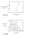
- FIGS. 13A–B show the leakage current for H plasma passivated W/HfO 2 /RTNO capacitors with an equivalent thickness of ⁇ 1 nm.
- FIG. 14 is an illustration of a cross-sectional view of a transistor of the present invention.
- FIGS. 15–22 are illustrations of a cross-sectional view of the fabrication of a transistor.
- FIG. 23 is an illustration of a cross-sectional view of a transistor of the present invention made using a metal gate self-aligned process.
- FIGS. 24–28 are illustrations of a cross-sectional view of the fabrication of a stack capacitor.
- FIG. 29 is an illustration of a cross-sectional view of a trench capacitor.
- the present invention broadly relates to chemical vapor deposition of hafnium oxide and/or zirconium oxide, and fabrication of an electronic device incorporating a film deposited by the inventive method. More specifically, the present invention relates broadly to chemical vapor deposition of hafnium oxide and/or zirconium oxide utilizing a hafnium or zirconium alkoxide precursor dissolved, emulsified or suspended in a liquid, vaporizing at least the alkoxide precursor, and depositing a constituent of the vaporized precursor on a substrate to form a film at a deposition temperature >400° C.
- the precursor employed in the present invention is defined as any hafnium or zirconium alkoxide. Mixtures containing the same or different metal are also contemplated herein.
- a generalized formula for the precursor of the present invention is M(OR) 4 where M is Zr or Hf, R is a ligand selected from linear or branched C 1-22 , preferably C 1-12 , alkyl or phenyl radicals.
- the preferred precursors are hafnium or zirconium isopropoxide, hafnium or zirconium sec-butoxide, hafnium or zirconium ethoxide, hafnium or zirconium isobutoxide, hafnium or zirconium methoxide, hafnium or zirconium propoxide, hafnium or zirconium butoxide, hafnium or zirconium tertiary butoxide, or hafnium or zirconium phenoxide.
- the liquid which is employed in the present invention is selected from aliphatic hydrocarbons, aromatic hydrocarbons, alcohols, ethers, aldehydes, ketones, acids, phenols, esters, amines, alkylnitrile, halgonated hydrocarbons, silyated hydrocarbons, thioethers, amines, cyanates, isocyanates, thiocyanates, silicone oils, nitroalkyl, alkylnitrate and/or mixtures of one or more of the above.
- the alkoxide precursor may be dissolved, emulsified or suspended in the liquid.
- the above-mentioned liquids are inert in that the liquid does not react substantially with the alkoxide precursor.
- the method of hafnium oxide and/or zirconium oxide deposition of the present invention can be used in any CVD process with any delivery means.
- the invention is not limited to a specific CVD apparatus or delivery system.
- Chemical vapor deposition (CVD) is defined as introduction of multiple reagents into a reactor either simultaneously or sequentially, digital chemical vapor deposition, pulsed chemical vapor deposition and other like methods.
- a liquid precursor mixture including the metal alkoxide precursor (or mixtures thereof) and the liquid is first provided.
- the liquid precursor mixture includes from about 0.05 to about 0.4 molar metal alkoxide precursor dissolved, suspended or emulsified in 100%, by weight, of the liquid. More preferably, the liquid precursor mixture includes from about 0.1 to about 0.2 molar metal alkoxide precursor dissolved, suspended or emulsified in 100%, by weight, of the liquid.
- the liquid precursor mixture may be formed outside the reactor chamber of a CVD deposition apparatus, or alternatively the mixture may be formed inside the reactor chamber itself.
- an inert gas such as He, Ar, Ne, Kr, Xe or mixtures thereof can be introduced in the portion of apparatus that includes the liquid precursor mixture.
- the flow rate of the liquid precursor mixture may be from about 40 to about 200 mg/min., with a flow rate of from about 5 to about 100 mg/min. being more preferred.
- dissolved is used in the present invention to denote that the metal alkoxide precursor is substantially distributed more or less evenly throughout the liquid.
- emulsified denotes that the metal alkoxide precursor is substantially dispersed in an immiscible liquid as droplets that are typically larger than colloidal size.
- sustained denotes that particles of the metal alkoxide precursor are mixed with, but not completely dissolved, in the liquid.
- the liquid precursor mixture thus formed is then vaporized in a vaporizer at a temperature of from about 25° to about 250° C., with a temperature of from about 50° to about 80° C. being more highly preferred. It is noted that the above temperatures are sufficiently high enough to at least vaporize the metal alkoxide precursor.
- the vaporization step may include only vaporization of the metal alkoxide, without vaporization of the liquid.
- the unvaporized liquid is typically, but not always, removed from the reactor in liquid form.
- the liquid and metal alkoxide precursor are vaporized together, i.e., they are co-vaporized.
- Anhydrous N 2 may be introduced in the vaporizer at a flow rate of from about 0 to about 1000 sccm, with a flow rate of from about 40 to about 800 sccm being more highly preferred.
- the vaporized precursor component is applied, via deposition, onto a substrate using a deposition temperature of greater than 400° C. More preferably, the deposition temperature is from about 450° to about 1000° C.
- the pressure during the growth of the inventive film of HfO 2 and/or ZrO 2 is from about 1 milliTorr to about 100 Torr, with a pressure of from about 0.3 to about 2 Torr being more highly preferred.
- the vaporized precursor may be used in the presence of a reactant gas, which includes an oxygen-containing source.
- Suitable reactant gases include, but are not limited to: oxygen, N 2 O, NO, H 2 O or ozone.
- a preferred reactant gas is oxygen.
- any CVD process (including apparatus and delivery systems) can be used in the present invention.
- substrate is used in the present invention to denote any semiconducting material such as, for example, Si, Ge, SiGe, InAs and the like; insulating materials including any inorganic dielectric or organic dielectric; or any conductive material including polysilicon, metal silicides, metal nitrides and elemental metals or alloys.
- substrate thus denotes any component of a front-end or back-end of the line device.
- the above deposition process results in the formation of a high-k oxide film of Zr, Hf or a mixture thereof onto the substrate.
- the thickness of the inventive film may vary depending on the deposition conditions and amount of metal alkoxide present in the vaporized precursor, but typically the inventive film has a thickness of from about 5 to about 5000 ⁇ .
- the inventive film is a dense film including a microcrystalline grain structure having a grain size of about 10 nm or less. More preferably, the inventive film has a grain size of from about 0.2 to about 6.5 nm.
- the inventive film contains little or no FTIR detectable amounts of C or OH.
- the film forms an atomically smooth interface with the underlying substrate.
- atomically smooth it is meant that the interface between the substrate and the deposited film is substantially continuous across the entire substrate.
- inventive film has improved surface roughness which means that substantially no defect regions such as divots are present on the upper surface of the inventive film
- a yet further characteristic feature of the inventive high-k oxide film is that the film is stable to reducing conditions necessary to passivate the underlying substrate. Without wishing to be bound by any theory, it is believed that this stabilization to reducing conditions is caused by the dense films of the present invention which contain little or no FTIR detectable amounts of C or OH.
- One aspect of the present invention relates broadly to fabrication of a structure of a complementary metal oxide semiconductor (CMOS) integrated circuit logic device incorporating hafnium oxide and/or zirconium oxide deposited by the inventive method. More specifically, the present invention relates to the fabrication of a CMOS integrated circuit that contains both n-type field effect transistors (NFET) and p-type field effect transistors (PFET) formed on a single substrate 10 . As shown in FIG. 1 , NFET device 11 is formed on a p-type conductivity region 13 of substrate 10 and contains a gate electrode 14 formed on a gate dielectric 15 and a pair of n-type source/drain regions 16 formed on laterally opposite sides of gate electrode 14 .
- CMOS complementary metal oxide semiconductor
- PFET device 17 is formed on a n-type conductivity region 18 of substrate 10 and contains the gate electrode 19 formed on gate dielectric 15 and a pair of p-type conductivity source/drain regions 20 formed along opposite sidewalls of gate electrode 19 .
- the NFET and PFET devices are separated by shallow trench isolation 21 and by spacers 22 .
- gate dielectric 15 incorporates hafnium oxide and/or zirconium oxide deposited by the inventive method.
- Another aspect of the present invention relates broadly to fabrication of a structure of an integrated circuit capacitor incorporating hafnium oxide and/or zirconium oxide deposited by the inventive method. More specifically, the present invention relates to the fabrication of a capacitor. As shown in FIG. 2 , a typical capacitor is formed on a substrate 30 , connected by a plug 31 to a transistor, with a barrier 32 and consists of a bottom electrode 33 , a dielectric material 34 , and a top electrode 35 .
- the dielectric material 34 incorporates hafnium oxide and/or zirconium oxide deposited by the inventive method.
- the capacitor may be stack or trench.
- the inventive high-k oxide film can be used in various electronic devices, it is preferred to use the high-k oxide in devices wherein a conductive material, such as, Ni, W, Mo, Ti, Cr, Te, Cu, Pd, Pt, Be, Au, Ir, Ta, Rh, Fe, Mn, Nb, V, Re, Ag, Bi, Cd, Ga, Hf, In, Y, Zr, TaN, TaSiN, TiAlN, TiSiN, TaWN, TiWN, TaAlN, NbN, ZrN, TaTiN, IrO 2 , SiC, TiNPt, TiAlN-PT, Ru, RuO 2 , RuPt, WSi, TiSi, dopped and undoped polysilicon, Al, IrO x , Os, OsO x , MoSi, ReO 2 , doped or undoped alloys, mixtures and mutilayers, preferably W, is formed thereon.
- the conductive material
- the high-k oxide film provides passivation during an H 2 plasma treatment process or a conventional forming gas anneal.
- Al reacts with trapped water at the Al/Hf and/or Zr oxide interface forming a thin Al 2 O 3 layer which releases H. The released H facilitates the passivation of the stack.
- the hafnium oxide films were deposited in a quartz horizontal hot wall CVD reactor equipped with a 1 ⁇ 3 ⁇ 8′′ quartz flow cell.
- the hafnium alkoxide source mixture was comprised of 40 grams of hafnium tert-butoxide Hf(t-OC4H 9 ) 4 and 1 liter of octane.
- a thin layer ( ⁇ 20 ⁇ ) of SiO x N y layer was deposited on the silicon wafer prior to growth of hafnium oxide.
- the hafnium alkoxide source mixture was flowed at 0.5–0.01 ml/min, preferably 0.05 ml/min.
- the vaporizer temperature was 120–180° C., preferably 120° C.
- Anhydrous nitrogen was introduced into the vaporizer at 20–2000 sccm, preferably 200 sccm as a carrier gas for the volatilized hafnium isopropoxide.
- a reactant gas selected from the group including, oxygen, N 2 O, NO, H 2 O, ozone, preferably, oxygen was introduced through a separate inlet as the reactant gas.
- the system pressure was 5 Torr during growth.
- the substrate was heated by an external high intensity infrared lamp and the susceptor was comprised of Hastalloy. The temperature of the susceptor was monitored by insertion of a thermocouple into the susceptor.
- Hafnium oxide was deposited at 300–700° C., preferably at temperatures >400° C.
- the hafnium oxide film deposited at 300° C. was not crystalline and absorption bands attributable to OH, H 2 O, CH and carbonate were observed.
- the hafnium oxide film deposited at 400° C. was crystalline but absorption bands attributable to OH, H 2 O, CH and carbonate were observed in the FTIR spectrum. However at deposition temperature of 500° C. and greater, absorption bands attributable to OH, H 2 O, CH and carbonate are not observed.
- annealing the HfO 2 film deposited at 400° C. and 600° C. at 1000° C. for 30 min in oxygen resulted in the formation of SiO 2 .
- Strong absorptions assignable to SiO 2 were observed at 1200 and 1080 cm ⁇ 1 and are ascribed to the LO and TO components of the asymmetric stretch of the SiO 4 unit, respectively.
- the absorption bands at 460 cm ⁇ 1 are attributed to skeletal network Si—O—Si symmetric bond bending.
- the remaining absorption bands are assigned to Hf—O stretching and bending vibrations.
- the relative calculated peak area under the Si—O peaks at 1200 and 1080 cm ⁇ 1 is 6.3 times the amount under the Hf—O peak at 512 cm ⁇ 1 .
- the relative calculated peak area under the Si—O peaks is only 3.5 times the amount under the Hf—O peak.
- Hafnium oxide deposited at temperatures less than 400° C. contains significant quantities of OH and/or absorbed water as observed in the FTIR spectra and are less dense, facilitating the formation of an interfacial oxide layer during post deposition annealing.
- the hafnium oxide films were deposited in a single wafer, lamp heated susceptor type CVD reactor equipped with a 300 mm showerhead as supplied by TEL. A liquid delivery system and vaporizer was used to introduce precursors into the reactor.
- the hafnium alkoxide source mixture was comprised of 40 grams of hafnium tert-butoxide and 1 liter of octane.
- a thin layer ( ⁇ 20 ⁇ ) of ultra-thin (SiO 2 ) oxide (UTO) or rapid thermal thin oxide containing nitrogen (RTNO) was deposited on the silicon wafer prior to growth of hafnium oxide.
- the hafnium alkoxide source mixture was flowed at between 1 and 400 mg/min, preferably 80.
- the vaporizer temperature was 30–300° C., preferably 50° C.
- Anhydrous nitrogen was introduced into the vaporizer at 10–2000 sccm, preferably 40 sccm as a carrier gas for the volatilized hafnium tert-butoxide.
- Oxygen was introduced through a separate inlet as the reactant gas.
- the system pressure was 1 mT to 100 Torr during growth, preferably 1.5 Torr.
- the substrate was heated by an external high intensity infrared lamp and the susceptor was comprised of AlN. The temperature of the susceptor was monitored by insertion of a thermocouple into the susceptor.
- Hafnium oxide was deposited at 250–850° C., preferably at 500° C.
- the liquid is not vaporized and is diverted from the CVD reactor.
- the hafnium alkoxide is dissolved, emulsified or suspended in a liquid which vaporizes at a higher temperature.
- the hafnium alkoxide and the liquid is introduced into a vaporizer where the hafnium alkoxide is vaporized.
- the liquid is not vaporized, but instead is diverted from the reactor in liquid form.
- FIG. 5 One possible apparatus configuration is shown in FIG. 5 .
- the hafnium alkoxide and liquid would flow from ampoule 100 to vaporizer 102 .
- the hafnium alkoxide is volatilized in the vaporizer, but the liquid would not.
- the vaporized hafnium alkoxide is then transported to reactor 106 , and the nonvaporized inert liquid is drained out of the vaporizer and collected in trap 04 .
- the vaporizer temperature is set at less than the boiling point of the liquid.
- Inlet 101 and outlet 103 are also shown, together with arrows which depict the flow within the reactor.
- hafnium isopropoxide and dodecane (boiling point 216° C.) with the vaporizer temperature set at 60° C., and the deposition temperature >400° C.
- FIG. 6 depicts a Al/HfO 2 /capacitor structure 150 that can be formed using the method of the present invention.
- a thin layer ( ⁇ 20 ⁇ ) of ultra-thin (SiO 2 ) oxide (UTO) or rapid thermal thin oxide 154 containing nitrogen (RTNO) was deposited on the silicon wafer 152 prior to growth of hafnium oxide.
- the hafnium oxide film 156 having a thickness of about 20 ⁇ was deposited as described in example 2.
- Capacitors were formed by Al 160 evaporation through a shadow Si mask with the substrates held at room temperature. Capacitor area is 5.6E ⁇ 4 cm 2 .
- the Al/HfO 2 /RTNO/Si stack was passivated by annealing in air at 315° C. It is theorized that when annealed in air at 315° C., the Al reacts with trapped water at the Al/HfO 2 interface to form a thin Al 2 O 3 layer 158 releasing H which passivates the gate stack.
- the nearly ideal capacitance voltage (CV) characteristics at 100 Khz are depicted in FIG. 7 for n and p type substrates.
- the flat band voltage is ⁇ 1V for p-type substrate and ⁇ 0.4V for the n type which are close to ideal.
- the HfO 2 was formed on an ultra-thin (SiO 2 ) oxide (UTO) and for the n-type the HfO 2 was formed on rapid thermal thin oxide containing nitrogen (RTNO).
- Hystersis is about 8 mV for the p-type and 14 mV for the n-type.
- the CV characteristics for a n-type capacitors which received no anneal is also shown in FIG. 7 . In this case, the flatband shift is about ⁇ 0.8V which is far from ideal when compared with the passivated capacitor.
- FIG. 8 shows CV characteristics for two different HfO 2 thicknesses. Note that the flat band voltage does not shift with film thickness indicating that the stack has low fixed charge and passivation has occurred at the bottom interface near the Si substrate.
- FIG. 9 shows the structure of a W/HfO 2 /RTNO capacitor 170 which can be formed using the inventive method.
- Vias are etched into blanket SiO 2 174 on n+Si 172 .
- the vias in the thick SiO 2 define the capacitor area.
- a thin layer ( ⁇ 20 ⁇ ) of ultra-thin (SiO 2 ) oxide (UTO) or rapid thermal thin oxide containing nitrogen (RTNO) 176 was deposited on the silicon wafer prior to growth of hafnium oxide 178 .
- the hafnium oxide films were deposited as described in example 2.
- the W top electrode 180 is deposited by chemical vapor deposition. The W is patterned by masking off the capacitor area with photoresist and etching the unmasked areas in a wet process.
- the capacitor is passivated by using a 13 MHz rf generated H plasma in a parallel plate configuration.
- the rf cathode was 8 inches in diameter.
- the substrate was grounded.
- Process was carried out at 0.1 mTorr to 100 torr, preferably, 100 mTorr with a substrate temperature between 25–900° C., preferably, 350° C., 1–1000 Watts, preferably, 100 Watts, for 1 s–6 hours, preferably 30 minutes.
- the CV characteristics of the W/HfO 2 /RTNO capacitor are shown in FIG. 10 . Before passivation the CV shows clear evidence of interface states. After the H plasma passivation, reduction of interface states is achieved.
- FIG. 11 shows the same stack capacitors W/HfO 2 /RTNO furnace annealed in forming gas (5% H2 in N2). In this case, best passivation was achieved by using a temperature of 600° C. for 30 m. Also as in the case of H plasma passivation, interface states are reduced as shown in FIG. 11 and W workfunction is ⁇ 4.74 eV.
- FIG. 12 shows charge trapping as a function of stress time at stress voltage of 1.5 V and varying temperatures (140° C. and 25° C.) for capacitors passivated by the Hydrogen plasma at 100 W for 30 minutes.
- the symbols are the measurements and solid lines are the model calculations for estimating lifetimes.
- the estimated lifetime at 10 years of stressing and operating conditions of 1.5 V and 140° C. meet the reliability specification for charge trapping.
- FIG. 13A shows leakage current for a passivated W/HfO 2 /RTNO capacitors with an equivalent quantum mechanical thickness of ⁇ 1 nm as calculated by S. H. Lo, et al., IEEE Electron Device Letters, 18, 209 (1997). Note that the leakage current is four orders of magnitude less than SiO 2 , See FIG. 13B .
- the inventive method is used to deposit hafnium or zirconium oxide as the gate dielectric layer 15 of the PFET and NFET as shown in FIG. 1 .
- a Si wafer substrate containing patterned structures is used. Selected regions of the substrate contain shallow trench isolation (STI) oxide located between the sites of transistor, other regions contain the field oxide, and selected regions of bare Si are exposed in the regions where transistor are to be located.
- the substrate is then placed in a suitable modular cluster tool, the surface of the bare Si is treated to form a SiO x N y layer in situ without breaking vacuum, before a layer of hafnium oxide is deposited to a thickness of 1–100 nm using the CVD process of this invention.
- the wafer is then transported to a second module of the modular cluster tool where the gate electrode can be deposited on the hafnium oxide and/or zirconium oxide in situ without breaking vacuum.
- the inventive method is used to deposit a multilayer gate dielectric, 53 where at least one of the layers is hafnium oxide and/or zirconium oxide doped or undoped.
- a transistor device is formed on a conductivity region 51 and contains a gate electrode 52 formed on a gate dielectric 53 and a pair of n-type source/drain regions 54 formed on laterally opposite sides of gate electrode 52 .
- the multilayer gate dielectric, 53 is comprised of an optional upper layer, 57 which may act as a dopant diffusion barrier and stabilize the structure during deposition of the gate electrode 52 .
- An optional lower layer, 55 which may act as an electron barrier layer and as a layer to prevent oxidation of the underlying silicon during processing or both.
- the middle layer, 56 is a high-K dielectric layer.
- a suitable lower layer 55 is composed of dielectric materials including, but not limited to: SiO 2 , SiO x N y , Si 3 N 4 , prepared from oxidation or nitridation of the silicon substrate or deposited separately. Other suitable lower layer materials include metal oxides or metal silicates.
- a high-K dielectric layer 56 selected from the group consisting of hafnium oxide and/or zirconium oxide or a multilayer structure where at least one of the layers is hafnium oxide and/or zirconium oxide.
- the dielectric materials comprising the multilayer structure with hafnium oxide and/or zirconium oxide are selected from the group including, but not limited to: Ta 2 O 5 , TiO 2 , ZrO 2 , HfO 2 , Al 2 O 3 , La 2 O 3 , Y 2 O 3 , yttrium alumnate, lathnaum alumnate, lanthanum silicate, yttrium silicate, hafnium silicate, zirconium silicate, doped or undoped mixtures, layers or combinations thereof.
- the multilayer structure with hafnium oxide and/or zirconium oxide may be comprised of several layers of different materials such as a layer of hafnium oxide and/or zirconium oxide sandwiched between layers of hafnium oxide and/or zirconium oxide.
- the optional upper layer 57 may be an oxidized or nitrided surface of the middle layer, or a deposited dielectric material including, but not limited to: SiO 2 , SiO x N y , Si 3 N 4 , ZrO 2 , HfO 2 , Al 2 O 3 , aluminosilicate, ytrrium silicate, zirconium silicate, hafnium silicate, lanthanum silicate doped or undoped mixtures, layers or combinations thereof
- Preferred gate dielectrics are comprised of a lower layer of SiO x N y , a layer of hafnium oxide and/or zirconium oxide, and an upper barrier layer of nitrided hafnium oxide and/or zirconium oxide.
- the hafnium oxide and/or zirconium oxide in the gate dielectric 53 is deposited by the inventive method.
- FIGS. 15 through 22 are cross sectional views showing one preferred fabrication of a transistor using the inventive method. Fabrication of the gate dielectric 53 is done in situ in a cluster tool as manufactured by TEL. In FIG. 15 a silicon substrate 50 with a clean (no native SiO 2 ) surface is the starting point. In FIG. 16 the lower layer 55 has been formed by oxidationlnitridation of the silicon substrate 50 to form a SiO x N y layer. In FIG. 16 , a layer 56 of hafnium oxide and/or zirconium oxide has been formed by the inventive method, comprised of depositing hafnium oxide and/or zirconium oxide by chemical vapor deposition at temperatures >400° C.
- the upper layer 57 is formed by plasma nitridation of the hafnium oxide and/or zirconium oxide surface.
- polysilicon is deposited as the gate electrode 52 .
- the gates are formed, extension implant done, spacers 58 formed, and source/drain implants performed to produce a fully formed devices. The subsequent steps of contact formation, etc. are not shown.
- FIG. 23 A possible metal gate self-aligned process is outlined below.
- the resultant structure is shown in FIG. 23 .
- the self-aligned process uses a replacement gate flow.
- a dielectric layer 1000 was deposited on top of a standard CMOS structure shown in FIG. 1 .
- the structure was then planarized by CMP, the poly Si n+ and p+ layers ( 14 and 19 ) and oxides ( 15 ) were then removed.
- the RTNO or UTO 1001 and HfO 2 1002 are deposited in the vias.
- Metal 15 a (NFET) and 16 a (PFET) were deposited on top of the HfO 2 .
- the via was finally filled with a suitable material 17 a , which may be a metal or an insulator.
- the structure was finally planarized using CMP.
- FIG. 23 shows the final integrated structure.
- the reference numerals not specifically mentioned herein are representative of the elements previously described in FIG. 1 .
- Materials suitable for the NFET gate electrode 16 a include, but not limited: to polysilicon, W, Mo, TiN, TaN, TaSiN, Fe, Mn, Nb, V, Ag, Bi, Cd, Fe, Ga, Hf, In, Mn, Y, Zr doped or undoped alloys, mixtures and multilayers, thereof.
- Materials suitable for the gate electrode 17 a for PFET include, but not limited to: polysilicon, Ni, W, Mo, Ti, TiN, Pd, Pt, Au, Ir, Rh, doped or undoped alloys, mixtures and multilayers, thereof.
- the gate dielectric 1002 hafnium oxide and/or zirconium oxide, was deposited by the inventive method as described in examples 1–5.
- an integrated circuit capacitor is fabricated incorporating hafnium oxide and/or zirconium oxide deposited by the inventive method.
- a typical capacitor is formed on a substrate 30 , connected by a plug 31 to a transistor, with a barrier 32 and consists of a bottom electrode 33 , a dielectric material 34 , and a top electrode 35 .
- the dielectric material, 34 hafnium oxide and/or zirconium oxide is deposited by the inventive method.
- FIGS. 24 through 28 are partial cross sectional views showing one example of a possible fabrication sequence for a capacitor.
- a substrate 30 having a trench is formed.
- Substrates include, but are not limited to Si-containing semiconductor substrates, silicon on insulator substrates, Ge substrates, SiGe substrates, GaAs substrates, and other like substrates, dielectrics, metals, organic substrates, glasses, metal oxides, plastic polymeric substrates and mixtures, combinations and layers thereof.
- a plug material 31 and an optional barrier 32 is formed.
- the plug material is composed of conventional conductive materials including, but not limited to: polysilicon, W, Mo, Ti, Cr, Cu, and may deposited utilizing the inventive method.
- the optional conductive barrier 32 is composed of conventional conductive materials including, but not limited to TaN, TaSiN, TiAlN, TiSiN, TaSiN, TaWN, TiWN, TaSiN, TaAlN, NbN, ZrN, TaTiN, TiSiN, TiAlN, IrO 2 , SiC, TiPt 2 , TiNPt, TiAlN-Pt, Ru, RuO 2 , RuPt, RuO 2 , WSi, Ti, TiSi, doped and undoped polysilicon, Al, Pd, Ir, IrO x , Os, OsO x , MoSi, TiSi, ReO 2 , mixtures or multilayers thereof and may be deposited utilizing the inventive method.
- conventional conductive materials including, but not limited to TaN, TaSiN, TiAlN, TiSiN, TaSiN, TaWN, TiWN, TaSiN, TaAlN, NbN
- a bottom electrode 33 is formed.
- the bottom electrode is composed of conductive materials including, but not limited to: polysilicon, Ni, Pd, Pt, Cu, Ag, Au, Ru, Ir, Rh, IrO x , RuO x , TaN, TaSiN, Ta, SrRuO 3 , LaSrCoO 3 , doped or undoped alloys, mixtures, or multilayer, thereof.
- a dielectric material 34 is formed.
- the dielectric material is selected from the group consisting of hafnium oxide and/or zirconium oxide or a multilayer structure where at least one of the layers is hafnium oxide and/or zirconium oxide.
- the dielectric materials comprising the multilayer structure with hafnium oxide and/or zirconium oxide are selected from any insulating material including, but not limited to: SiO 2 , SiO x N y , Si 3 N 4 , metal oxides such as Ta 2 O 5 , TiO 2 , ZrO 2 , HfO 2 , La 2 O 3 , Y 2 O 3 mixtures or layers thereof, or multicomponent metal oxides such as pervoskite type oxide having the formula ABO 3 wherein B is at least one acid oxide containing a metal selected from the group consisting of Al, Ti, Zr, Hf, V, Nb, Ta, Cr, Mo, W and Cu, and A is at least one additional cation having a positive formal charge of from about 1 to about 3.
- insulating material including, but not limited to: SiO 2 , SiO x N y , Si 3 N 4 , metal oxides such as Ta 2 O 5 , TiO 2 , ZrO 2 , HfO 2
- Examples include but are not limited to: barium strontium titanate, zirconate, hafnate, lead titanate, yttrium alumnate, lanthanum alumnate, lead zirconium titanate, silicates such as hafnium silicate, zirconium silicate including rare earth doped silicates.
- a top electrode 35 is formed.
- the top electrode is composed of conductive materials including, but not limited to: polysilicon, Ni, Pd, Pt, Cu, Ag, Au, Ru, Ir, Rh,IrO x , RuO x , TaN, TaSiN, Ta, SrRuO 3 , LaSrCoO 3 , doped or undoped alloys, mixtures, or multilayer, thereof.
- the top and bottom electrode may or may not be similar.
- the dielectric material 34 hafnium oxide and/or zirconium oxide, is deposited by the inventive method.
- an integrated circuit trench capacitor is fabricated incorporating at least one component deposited by the inventive method.
- One possible example for fabricating a trench capacitor on a substrate 30 is shown in FIG. 29 .
- a capacitor recess is formed in the substrate 30 which is connected to underlying circuitry via plug 31 .
- the circuitry is covered with a dielectric insulating layer (isolation dielectric) 83 .
- Substrates include, but are not limited to Si-containing semiconductor substrates, silicon on insulator substrates, Ge substrates, SiGe substrates, GaAs substrates, and other like substrates, dielectrics, metals, organic substrates, glasses, metal oxides, plastic polymeric substrates and mixtures, combinations and layers thereof.
- the dielectric insulating layer (isolation dielectric) 83 is selected from any insulating material including, but not limited to: SiO 2 , SiO x N y , Si 3 N 4 , phosphosilicate glass, or metal oxides such as hafnium oxide and/or zirconium oxide doped or undoped mixtures, or multilayer, thereof.
- the plug material is composed of conventional conductive materials including, but not limited to: polysilicon, W, Mo, Ti, Cr, Cu, and may deposited utilizing the inventive method.
- the optional conductive barrier 32 is composed of conventional conductive materials including, but not limited to TaN, TaSiN, TiAlN, TiSiN, TaSiN, TaWN, TiWN, TaSiN, TaAlN, NbN, ZrN, TaTiN, TiSiN, TiAlN, IrO 2 , SiC, TiPt, TiNPt, TiAlN-Pt, Ru, RuO 2 , RuPt, RuO 2 , WSi, Ti, TiSi, doped and undoped polysilicon, Al, Pd, Ir, IrO x , Os, OsO x , MoSi, TiSi, ReO 2 , mixtures or multilayers thereof and may be deposited utilizing the inventive method.
- conventional conductive materials including, but not limited to TaN, TaSiN, TiAlN, TiSiN, TaSiN, TaWN, TiWN, TaSiN, TaAlN, NbN, Z
- the bottom electrode 33 is composed of conductive materials including, but not limited to: polysilicon, Ni, Pd, Pt, Cu, Ag, Au, Ru, Ir, Rh,IrO x , RuO x , TaN, TaSiN, Ta, SrRuO 3 , LaSrCoO 3 , doped or undoped alloys, mixtures, or multilayer, thereof.
- the dielectric material, 34 is selected from the group consisting of hafnium oxide and/or zirconium oxide or a multilayer structure where at least one of the layers is hafnium oxide and/or zirconium oxide.
- the dielectric materials comprising the multilayer structure with hafnium oxide and/or zirconium oxide are selected from any insulating material including, but not limited to: SiO 2 , SiO x N y , Si 3 N 4 , metal oxides such as Ta 2 O 5 , TiO 2 , ZrO 2 , HfO 2 , Al 2 O 3 , La 2 O 3 , Y 2 O 3 alloys, mixtures or layers thereof, or multicomponent metal oxides such as pervoskite type oxide having the formula ABO 3 wherein B is at least one acid oxide containing a metal selected from the group consisting of Al, Ti, Zr, Hf, V, Nb, Ta, Cr, Mo, W and Cu, and A is at least one additional cation having a positive formal charge of from about 1 to about 3.
- insulating material including, but not limited to: SiO 2 , SiO x N y , Si 3 N 4 , metal oxides such as Ta 2 O 5 , TiO 2 , Z
- the top electrode 35 is composed of conductive materials including, but not limited to: polysilicon, Ni, Pd, Pt, Cu, Ag, Au, Ru, Ir, Rh,IrO x , RuO x , TaN, TaSiN, Ta, SrRuO 3 , LaSrCoO 3 , doped or undoped alloys, mixtures, or multilayer, thereof.
- the top and bottom electrode may or may not be similar.
- the optional dielectric barrier is composed of any insulating material including, but not limited to SiO 2 , SiO x N y , Si 3 N 4 , TiON, AlN, SiN, TiN, metal oxides such as Ta 2 O 5 , TiO 2 , ZrO 2 , HfO 2 , Al 2 O 3 , La 2 O 3 , Y 2 O 3 , alloys, mixtures or layers thereof, or multicomponent metal oxides.
- the sequentially deposited layers are planarized to yield a trench capacitor in the capacitor recess.
- the insulating passivation layer 37 is composed of any insulating material including, but not limited to SiO 2 , SiO x N y , Si 3 N 4 , TiON, AlN, SiN, TiN, metal oxides such as Ta 2 O 5 , TiO 2 , ZrO 2 , HfO 2 , Al 2 O 3 , oxide, La 2 O 3 , Y 2 O 3 , alloys, mixtures or layers thereof, or multicomponent metal oxides.
- the inter-layer dielectric 38 is selected from any insulating material including, but not limited to: SiO 2 , SiO x N y , Si 3 N 4 , phosphosilicate glass, or metal oxides such as hafnium oxide and/or zirconium oxide doped or undoped mixtures, or multilayer, thereof.
- a via is formed in the barrier structure.
- a diffusion barrier layer 81 and a metallazation layer 82 is deposited over the barrier structure and via.
- the diffusion barrier layer 81 includes, but not limited to: WN, TiN, or TaN.
- the metallazation layer 82 is selected from any conductive material including, but not limited to: Al, W, Mo, Ti, Cr, or Cu doped or undoped alloys, mixtures, or layers thereof.
- the dielectric material 34 hafnium oxide and/or zirconium oxide, is deposited by the inventive method, optionally hafnium oxide and/or zirconium oxide may be utilized as the dielectric including, but not limited to insulating passivation layer, inter-layer dielectric, diffusion barrier layer, isolation dielectric.
Abstract
Description
t eq =t phy(∈SiO2/∈high-k)
where tphy is the actual thickness of the substitute metal oxide gate dielectric, such as hafnium oxide, zirconium oxide, aluminum oxide, lanthanum oxide, yttrium oxide, lanthanum aluminum oxide, and the like, and where ∈SiO2 and ∈high-k are the dielectric constants of SiO2 and the metal oxide gate dielectric film, respectively. Similar problems are encountered in scaling capacitors in memory devices. As the circuits become denser and the devices smaller, a material with a higher capacitance, such as HfO2, ZrO2, or Al2O3, is necessary to store adequate charge in the capacitor. High-k dielectrics, such as HfO2, ZrO2, or Al2O3, have dielectric constants more than double the dielectric constant of SiO2 (k=4) and are thus an attractive material for replacement of SiO2 in transistors and capacitors. The term “high-k” denotes a dielectric having a dielectric constant of greater than SiO2, preferably 7 or above.
Claims (14)
M(OR)4
Priority Applications (2)
| Application Number | Priority Date | Filing Date | Title |
|---|---|---|---|
| US10/291,334 US6982230B2 (en) | 2002-11-08 | 2002-11-08 | Deposition of hafnium oxide and/or zirconium oxide and fabrication of passivated electronic structures |
| US11/281,032 US7566938B2 (en) | 2002-11-08 | 2005-11-17 | Deposition of hafnium oxide and/or zirconium oxide and fabrication of passivated electronic structures |
Applications Claiming Priority (1)
| Application Number | Priority Date | Filing Date | Title |
|---|---|---|---|
| US10/291,334 US6982230B2 (en) | 2002-11-08 | 2002-11-08 | Deposition of hafnium oxide and/or zirconium oxide and fabrication of passivated electronic structures |
Related Child Applications (1)
| Application Number | Title | Priority Date | Filing Date |
|---|---|---|---|
| US11/281,032 Division US7566938B2 (en) | 2002-11-08 | 2005-11-17 | Deposition of hafnium oxide and/or zirconium oxide and fabrication of passivated electronic structures |
Publications (2)
| Publication Number | Publication Date |
|---|---|
| US20040092073A1 US20040092073A1 (en) | 2004-05-13 |
| US6982230B2 true US6982230B2 (en) | 2006-01-03 |
Family
ID=32229244
Family Applications (2)
| Application Number | Title | Priority Date | Filing Date |
|---|---|---|---|
| US10/291,334 Expired - Fee Related US6982230B2 (en) | 2002-11-08 | 2002-11-08 | Deposition of hafnium oxide and/or zirconium oxide and fabrication of passivated electronic structures |
| US11/281,032 Expired - Fee Related US7566938B2 (en) | 2002-11-08 | 2005-11-17 | Deposition of hafnium oxide and/or zirconium oxide and fabrication of passivated electronic structures |
Family Applications After (1)
| Application Number | Title | Priority Date | Filing Date |
|---|---|---|---|
| US11/281,032 Expired - Fee Related US7566938B2 (en) | 2002-11-08 | 2005-11-17 | Deposition of hafnium oxide and/or zirconium oxide and fabrication of passivated electronic structures |
Country Status (1)
| Country | Link |
|---|---|
| US (2) | US6982230B2 (en) |
Cited By (43)
| Publication number | Priority date | Publication date | Assignee | Title |
|---|---|---|---|---|
| US20030004744A1 (en) * | 2000-05-22 | 2003-01-02 | Greene William S. | Method and system for implementing a Global Information Bus in a global ecosystem of interrelated services |
| US20040105935A1 (en) * | 2002-11-12 | 2004-06-03 | Park Young Hoon | Method of depositing thin film using hafnium compound |
| US20050062130A1 (en) * | 2003-09-23 | 2005-03-24 | Anthony Ciancio | Semiconductor device and making thereof |
| US20050260347A1 (en) * | 2004-05-21 | 2005-11-24 | Narwankar Pravin K | Formation of a silicon oxynitride layer on a high-k dielectric material |
| US20060001151A1 (en) * | 2003-03-04 | 2006-01-05 | Micron Technology, Inc. | Atomic layer deposited dielectric layers |
| US20060024975A1 (en) * | 2004-08-02 | 2006-02-02 | Micron Technology, Inc. | Atomic layer deposition of zirconium-doped tantalum oxide films |
| US20060043492A1 (en) * | 2004-08-26 | 2006-03-02 | Micron Technology, Inc. | Ruthenium gate for a lanthanide oxide dielectric layer |
| US20060160303A1 (en) * | 2005-01-20 | 2006-07-20 | Chartered Semiconductor Manufacturing Ltd | Method for forming high-K charge storage device |
| US20060223337A1 (en) * | 2005-03-29 | 2006-10-05 | Micron Technology, Inc. | Atomic layer deposited titanium silicon oxide films |
| US20060244082A1 (en) * | 2005-04-28 | 2006-11-02 | Micron Technology, Inc. | Atomic layer desposition of a ruthenium layer to a lanthanide oxide dielectric layer |
| US20060261397A1 (en) * | 2003-06-24 | 2006-11-23 | Micron Technology, Inc. | Lanthanide oxide/hafnium oxide dielectric layers |
| US20060270147A1 (en) * | 2005-05-27 | 2006-11-30 | Micron Technology, Inc. | Hafnium titanium oxide films |
| US20060267066A1 (en) * | 2004-08-31 | 2006-11-30 | Jiutao Li | High dielectric constant transition metal oxide materials |
| US20070048953A1 (en) * | 2005-08-30 | 2007-03-01 | Micron Technology, Inc. | Graded dielectric layers |
| US20070048926A1 (en) * | 2005-08-31 | 2007-03-01 | Micron Technology, Inc. | Lanthanum aluminum oxynitride dielectric films |
| US20070049023A1 (en) * | 2005-08-29 | 2007-03-01 | Micron Technology, Inc. | Zirconium-doped gadolinium oxide films |
| US20070059881A1 (en) * | 2003-03-31 | 2007-03-15 | Micron Technology, Inc. | Atomic layer deposited zirconium aluminum oxide |
| US20070059948A1 (en) * | 2002-06-14 | 2007-03-15 | Metzner Craig R | Ald metal oxide deposition process using direct oxidation |
| US20070092989A1 (en) * | 2005-08-04 | 2007-04-26 | Micron Technology, Inc. | Conductive nanoparticles |
| US20070090441A1 (en) * | 2004-08-31 | 2007-04-26 | Micron Technology, Inc. | Titanium aluminum oxide films |
| US20070181931A1 (en) * | 2005-01-05 | 2007-08-09 | Micron Technology, Inc. | Hafnium tantalum oxide dielectrics |
| US20070212896A1 (en) * | 2006-03-09 | 2007-09-13 | Applied Materials, Inc. | Method and apparatus for fabricating a high dielectric constant transistor gate using a low energy plasma system |
| US20070212895A1 (en) * | 2006-03-09 | 2007-09-13 | Thai Cheng Chua | Method and apparatus for fabricating a high dielectric constant transistor gate using a low energy plasma system |
| US20070218623A1 (en) * | 2006-03-09 | 2007-09-20 | Applied Materials, Inc. | Method of fabricating a high dielectric constant transistor gate using a low energy plasma apparatus |
| US20070259111A1 (en) * | 2006-05-05 | 2007-11-08 | Singh Kaushal K | Method and apparatus for photo-excitation of chemicals for atomic layer deposition of dielectric film |
| US20080076268A1 (en) * | 2006-09-26 | 2008-03-27 | Applied Materials, Inc. | Fluorine plasma treatment of high-k gate stack for defect passivation |
| US20080173242A1 (en) * | 2007-01-24 | 2008-07-24 | Yuri Makarov | Method, system, and apparatus for the growth of SiC and related or similar material, by chemical vapor deposition, using precursors in modified cold-wall reactor |
| US20080173239A1 (en) * | 2007-01-24 | 2008-07-24 | Yuri Makarov | Method, system, and apparatus for the growth of SiC and related or similar material, by chemical vapor deposition, using precursors in modified cold-wall reactor |
| US20080261368A1 (en) * | 2007-04-20 | 2008-10-23 | Manfred Ramin | Work function adjustment with the implant of lanthanides |
| US20090068807A1 (en) * | 2007-09-07 | 2009-03-12 | Karve Gauri V | Dual gate oxide device integration |
| US20090101956A1 (en) * | 2007-10-17 | 2009-04-23 | International Business Machines Corporation | Embedded trench capacitor having a high-k node dielectric and a metallic inner electrode |
| US20090173991A1 (en) * | 2005-08-04 | 2009-07-09 | Marsh Eugene P | Methods for forming rhodium-based charge traps and apparatus including rhodium-based charge traps |
| US20100015765A1 (en) * | 2008-07-18 | 2010-01-21 | James William Adkisson | Shallow and deep trench isolation structures in semiconductor integrated circuits |
| US20100164064A1 (en) * | 2008-12-31 | 2010-07-01 | Hyun Dong Kim | Capacitor and Method for Manufacturing the Same |
| US20110037117A1 (en) * | 2004-08-31 | 2011-02-17 | Ahn Kie Y | Lanthanum-metal oxide dielectric apparatus, methods, and systems |
| US7927948B2 (en) | 2005-07-20 | 2011-04-19 | Micron Technology, Inc. | Devices with nanocrystals and methods of formation |
| US20120146160A1 (en) * | 2010-12-10 | 2012-06-14 | Globalfoundries Singapore Pte. Ltd. | High-k metal gate device |
| US20120287553A1 (en) * | 2011-05-13 | 2012-11-15 | Intermolecular, Inc. | Method for fabricating a dram capacitor having increased thermal and chemical stability |
| US9299802B2 (en) | 2012-10-28 | 2016-03-29 | International Business Machines Corporation | Method to improve reliability of high-K metal gate stacks |
| US9653534B2 (en) | 2014-12-17 | 2017-05-16 | International Business Machines Corporation | Trench metal-insulator-metal capacitor with oxygen gettering layer |
| US9714262B2 (en) | 2012-07-19 | 2017-07-25 | Hitachi Chemical Company, Ltd. | Composition for forming passivation layer, semiconductor substrate having passivation layer, method of producing semiconductor substrate having passivation layer, photovoltaic cell element, method of producing photovoltaic cell element and photovoltaic cell |
| US10825893B2 (en) | 2017-11-28 | 2020-11-03 | Samsung Electronics Co., Ltd. | Semiconductor devices |
| US11230098B2 (en) | 2018-05-11 | 2022-01-25 | Hewlett-Packard Development Company, L.P. | Passivation stacks |
Families Citing this family (324)
| Publication number | Priority date | Publication date | Assignee | Title |
|---|---|---|---|---|
| TW538500B (en) * | 2002-06-12 | 2003-06-21 | Nanya Technology Corp | Method of manufacturing gate of field effect transistor |
| JP4358492B2 (en) * | 2002-09-25 | 2009-11-04 | レール・リキード−ソシエテ・アノニム・プール・レテュード・エ・レクスプロワタシオン・デ・プロセデ・ジョルジュ・クロード | Method for producing silicon nitride film or silicon oxynitride film by thermal chemical vapor deposition |
| DE10255841A1 (en) * | 2002-11-29 | 2004-06-17 | Infineon Technologies Ag | Process for structuring ruthenium or ruthenium (IV) oxide layers used for a trench capacitor comprises depositing ruthenium or ruthenium (IV) oxide on sections of a substrate, depositing a covering layer, and further processing |
| US7101813B2 (en) | 2002-12-04 | 2006-09-05 | Micron Technology Inc. | Atomic layer deposited Zr-Sn-Ti-O films |
| US20040168627A1 (en) * | 2003-02-27 | 2004-09-02 | Sharp Laboratories Of America, Inc. | Atomic layer deposition of oxide film |
| JP4507232B2 (en) * | 2003-03-24 | 2010-07-21 | ローム株式会社 | Manufacturing method of semiconductor device |
| US7183186B2 (en) | 2003-04-22 | 2007-02-27 | Micro Technology, Inc. | Atomic layer deposited ZrTiO4 films |
| US6939815B2 (en) * | 2003-08-28 | 2005-09-06 | Intel Corporation | Method for making a semiconductor device having a high-k gate dielectric |
| US7205247B2 (en) * | 2003-09-30 | 2007-04-17 | Aviza Technology, Inc. | Atomic layer deposition of hafnium-based high-k dielectric |
| US7247534B2 (en) * | 2003-11-19 | 2007-07-24 | International Business Machines Corporation | Silicon device on Si:C-OI and SGOI and method of manufacture |
| KR100519800B1 (en) * | 2004-01-13 | 2005-10-10 | 삼성전자주식회사 | method of fabricating Lanthanum oxide layer and method of fabricating MOSFET transistor and capacitor using the same |
| DE102004005385A1 (en) * | 2004-02-03 | 2005-10-20 | Infineon Technologies Ag | Use of dissolved hafnium alkoxides or zirconium alkoxides as precursors for hafnium oxide and hafnium oxynitride layers or zirconium oxide and zirconium oxynitride layers |
| US8399934B2 (en) * | 2004-12-20 | 2013-03-19 | Infineon Technologies Ag | Transistor device |
| US7141857B2 (en) * | 2004-06-30 | 2006-11-28 | Freescale Semiconductor, Inc. | Semiconductor structures and methods of fabricating semiconductor structures comprising hafnium oxide modified with lanthanum, a lanthanide-series metal, or a combination thereof |
| JP4938262B2 (en) * | 2004-08-25 | 2012-05-23 | ルネサスエレクトロニクス株式会社 | Semiconductor device and manufacturing method thereof |
| US20060051975A1 (en) * | 2004-09-07 | 2006-03-09 | Ashutosh Misra | Novel deposition of SiON dielectric films |
| US7374984B2 (en) * | 2004-10-29 | 2008-05-20 | Randy Hoffman | Method of forming a thin film component |
| KR100647484B1 (en) * | 2004-11-23 | 2006-11-23 | 삼성전자주식회사 | method of forming a thin film layer, and method of forming a gate structure, capacitor and flash memory device using the same |
| US7235501B2 (en) | 2004-12-13 | 2007-06-26 | Micron Technology, Inc. | Lanthanum hafnium oxide dielectrics |
| JP2006278550A (en) * | 2005-03-28 | 2006-10-12 | Fujitsu Ltd | Manufacturing method of semiconductor device |
| TW200731404A (en) * | 2005-04-07 | 2007-08-16 | Aviza Tech Inc | Multilayer, multicomponent high-k films and methods for depositing the same |
| JP2006344836A (en) * | 2005-06-09 | 2006-12-21 | Matsushita Electric Ind Co Ltd | Semiconductor apparatus and manufacturing method thereof |
| DE102005030585B4 (en) * | 2005-06-30 | 2011-07-28 | Globalfoundries Inc. | Semiconductor device with a vertical decoupling capacitor and method for its production |
| GB2442400B (en) * | 2005-06-30 | 2010-09-29 | Advanced Micro Devices Inc | A semiconductor device including a vertical decoupling capacitor |
| KR100718835B1 (en) * | 2005-09-13 | 2007-05-16 | 삼성전자주식회사 | semiconductor MOS transistor and method of manufacturing the same |
| US20070120186A1 (en) * | 2005-11-29 | 2007-05-31 | Synopsys, Inc. | Engineered barrier layer and gate gap for transistors with negative differential resistance |
| US7592251B2 (en) * | 2005-12-08 | 2009-09-22 | Micron Technology, Inc. | Hafnium tantalum titanium oxide films |
| US7972974B2 (en) | 2006-01-10 | 2011-07-05 | Micron Technology, Inc. | Gallium lanthanide oxide films |
| US7709402B2 (en) | 2006-02-16 | 2010-05-04 | Micron Technology, Inc. | Conductive layers for hafnium silicon oxynitride films |
| US20070209930A1 (en) * | 2006-03-09 | 2007-09-13 | Applied Materials, Inc. | Apparatus for fabricating a high dielectric constant transistor gate using a low energy plasma system |
| US7727908B2 (en) | 2006-08-03 | 2010-06-01 | Micron Technology, Inc. | Deposition of ZrA1ON films |
| JP5142494B2 (en) * | 2006-08-03 | 2013-02-13 | ルネサスエレクトロニクス株式会社 | Manufacturing method of semiconductor device |
| US7759747B2 (en) | 2006-08-31 | 2010-07-20 | Micron Technology, Inc. | Tantalum aluminum oxynitride high-κ dielectric |
| US7776765B2 (en) | 2006-08-31 | 2010-08-17 | Micron Technology, Inc. | Tantalum silicon oxynitride high-k dielectrics and metal gates |
| US7605030B2 (en) | 2006-08-31 | 2009-10-20 | Micron Technology, Inc. | Hafnium tantalum oxynitride high-k dielectric and metal gates |
| US7544604B2 (en) | 2006-08-31 | 2009-06-09 | Micron Technology, Inc. | Tantalum lanthanide oxynitride films |
| KR20080046438A (en) * | 2006-11-22 | 2008-05-27 | 삼성전자주식회사 | Semiconductor device and method of fabricating the same |
| JP2008198763A (en) * | 2007-02-13 | 2008-08-28 | Matsushita Electric Ind Co Ltd | Semiconductor device and manufacturing method thereof |
| TWI459471B (en) * | 2007-03-08 | 2014-11-01 | Applied Materials Inc | Method and apparatus for fabricating a high dielectric constant transistor gate using a low energy plasma system |
| KR100909967B1 (en) * | 2007-06-08 | 2009-07-29 | 삼성전자주식회사 | Manufacturing method of semiconductor device |
| JP2009133000A (en) * | 2007-10-30 | 2009-06-18 | Fujifilm Corp | Silicon-nitrogen compound film, and gas-barrier film and thin-film device using the silicon-nitrogen compound film |
| US9394608B2 (en) | 2009-04-06 | 2016-07-19 | Asm America, Inc. | Semiconductor processing reactor and components thereof |
| US7943457B2 (en) * | 2009-04-14 | 2011-05-17 | International Business Machines Corporation | Dual metal and dual dielectric integration for metal high-k FETs |
| US8802201B2 (en) * | 2009-08-14 | 2014-08-12 | Asm America, Inc. | Systems and methods for thin-film deposition of metal oxides using excited nitrogen-oxygen species |
| KR101800844B1 (en) | 2010-04-23 | 2017-11-23 | 가부시키가이샤 한도오따이 에네루기 켄큐쇼 | Method for manufacturing semiconductor device |
| US20110298089A1 (en) * | 2010-06-03 | 2011-12-08 | International Business Machines Corporation | Trench capacitor and method of fabrication |
| US8633119B2 (en) | 2011-05-10 | 2014-01-21 | Applied Materials, Inc. | Methods for manufacturing high dielectric constant films |
| US8633114B2 (en) * | 2011-05-10 | 2014-01-21 | Applied Materials, Inc. | Methods for manufacturing high dielectric constant films |
| US9312155B2 (en) | 2011-06-06 | 2016-04-12 | Asm Japan K.K. | High-throughput semiconductor-processing apparatus equipped with multiple dual-chamber modules |
| US10854498B2 (en) | 2011-07-15 | 2020-12-01 | Asm Ip Holding B.V. | Wafer-supporting device and method for producing same |
| US20130023129A1 (en) | 2011-07-20 | 2013-01-24 | Asm America, Inc. | Pressure transmitter for a semiconductor processing environment |
| US9017481B1 (en) | 2011-10-28 | 2015-04-28 | Asm America, Inc. | Process feed management for semiconductor substrate processing |
| US9112003B2 (en) | 2011-12-09 | 2015-08-18 | Asm International N.V. | Selective formation of metallic films on metallic surfaces |
| KR101690392B1 (en) | 2011-12-20 | 2016-12-27 | 인텔 코포레이션 | Conformal low temperature hermetic dielectric diffusion barriers |
| US10714315B2 (en) | 2012-10-12 | 2020-07-14 | Asm Ip Holdings B.V. | Semiconductor reaction chamber showerhead |
| US9337296B2 (en) * | 2013-07-22 | 2016-05-10 | GlobalFoundries, Inc. | Integrated circuits having a metal gate structure and methods for fabricating the same |
| TWI661072B (en) | 2014-02-04 | 2019-06-01 | 荷蘭商Asm Ip控股公司 | Selective deposition of metals, metal oxides, and dielectrics |
| CN103898844B (en) * | 2014-02-20 | 2016-01-13 | 长沙理工大学 | A kind of slabstone buttress reinforced earth compound embankment culvert pipe structure |
| US10683571B2 (en) | 2014-02-25 | 2020-06-16 | Asm Ip Holding B.V. | Gas supply manifold and method of supplying gases to chamber using same |
| US10167557B2 (en) | 2014-03-18 | 2019-01-01 | Asm Ip Holding B.V. | Gas distribution system, reactor including the system, and methods of using the same |
| US11015245B2 (en) | 2014-03-19 | 2021-05-25 | Asm Ip Holding B.V. | Gas-phase reactor and system having exhaust plenum and components thereof |
| US10047435B2 (en) | 2014-04-16 | 2018-08-14 | Asm Ip Holding B.V. | Dual selective deposition |
| US10858737B2 (en) | 2014-07-28 | 2020-12-08 | Asm Ip Holding B.V. | Showerhead assembly and components thereof |
| US9890456B2 (en) | 2014-08-21 | 2018-02-13 | Asm Ip Holding B.V. | Method and system for in situ formation of gas-phase compounds |
| US9657845B2 (en) | 2014-10-07 | 2017-05-23 | Asm Ip Holding B.V. | Variable conductance gas distribution apparatus and method |
| US10941490B2 (en) | 2014-10-07 | 2021-03-09 | Asm Ip Holding B.V. | Multiple temperature range susceptor, assembly, reactor and system including the susceptor, and methods of using the same |
| US9490145B2 (en) | 2015-02-23 | 2016-11-08 | Asm Ip Holding B.V. | Removal of surface passivation |
| US10276355B2 (en) | 2015-03-12 | 2019-04-30 | Asm Ip Holding B.V. | Multi-zone reactor, system including the reactor, and method of using the same |
| US10458018B2 (en) | 2015-06-26 | 2019-10-29 | Asm Ip Holding B.V. | Structures including metal carbide material, devices including the structures, and methods of forming same |
| US10600673B2 (en) | 2015-07-07 | 2020-03-24 | Asm Ip Holding B.V. | Magnetic susceptor to baseplate seal |
| US9356125B1 (en) * | 2015-07-28 | 2016-05-31 | United Microelectronics Corp. | Manufacturing method of semiconductor structure |
| US10428421B2 (en) * | 2015-08-03 | 2019-10-01 | Asm Ip Holding B.V. | Selective deposition on metal or metallic surfaces relative to dielectric surfaces |
| US10121699B2 (en) | 2015-08-05 | 2018-11-06 | Asm Ip Holding B.V. | Selective deposition of aluminum and nitrogen containing material |
| US10566185B2 (en) | 2015-08-05 | 2020-02-18 | Asm Ip Holding B.V. | Selective deposition of aluminum and nitrogen containing material |
| US10695794B2 (en) | 2015-10-09 | 2020-06-30 | Asm Ip Holding B.V. | Vapor phase deposition of organic films |
| US10814349B2 (en) | 2015-10-09 | 2020-10-27 | Asm Ip Holding B.V. | Vapor phase deposition of organic films |
| US10211308B2 (en) | 2015-10-21 | 2019-02-19 | Asm Ip Holding B.V. | NbMC layers |
| US11139308B2 (en) | 2015-12-29 | 2021-10-05 | Asm Ip Holding B.V. | Atomic layer deposition of III-V compounds to form V-NAND devices |
| US10529554B2 (en) | 2016-02-19 | 2020-01-07 | Asm Ip Holding B.V. | Method for forming silicon nitride film selectively on sidewalls or flat surfaces of trenches |
| US10865475B2 (en) | 2016-04-21 | 2020-12-15 | Asm Ip Holding B.V. | Deposition of metal borides and silicides |
| US10190213B2 (en) | 2016-04-21 | 2019-01-29 | Asm Ip Holding B.V. | Deposition of metal borides |
| US10032628B2 (en) | 2016-05-02 | 2018-07-24 | Asm Ip Holding B.V. | Source/drain performance through conformal solid state doping |
| US10367080B2 (en) | 2016-05-02 | 2019-07-30 | Asm Ip Holding B.V. | Method of forming a germanium oxynitride film |
| US11081342B2 (en) | 2016-05-05 | 2021-08-03 | Asm Ip Holding B.V. | Selective deposition using hydrophobic precursors |
| US11453943B2 (en) | 2016-05-25 | 2022-09-27 | Asm Ip Holding B.V. | Method for forming carbon-containing silicon/metal oxide or nitride film by ALD using silicon precursor and hydrocarbon precursor |
| US10373820B2 (en) | 2016-06-01 | 2019-08-06 | Asm Ip Holding B.V. | Deposition of organic films |
| US10453701B2 (en) | 2016-06-01 | 2019-10-22 | Asm Ip Holding B.V. | Deposition of organic films |
| US9803277B1 (en) | 2016-06-08 | 2017-10-31 | Asm Ip Holding B.V. | Reaction chamber passivation and selective deposition of metallic films |
| US10612137B2 (en) | 2016-07-08 | 2020-04-07 | Asm Ip Holdings B.V. | Organic reactants for atomic layer deposition |
| US9859151B1 (en) | 2016-07-08 | 2018-01-02 | Asm Ip Holding B.V. | Selective film deposition method to form air gaps |
| US10714385B2 (en) | 2016-07-19 | 2020-07-14 | Asm Ip Holding B.V. | Selective deposition of tungsten |
| US9812320B1 (en) | 2016-07-28 | 2017-11-07 | Asm Ip Holding B.V. | Method and apparatus for filling a gap |
| US9887082B1 (en) | 2016-07-28 | 2018-02-06 | Asm Ip Holding B.V. | Method and apparatus for filling a gap |
| KR102532607B1 (en) | 2016-07-28 | 2023-05-15 | 에이에스엠 아이피 홀딩 비.브이. | Substrate processing apparatus and method of operating the same |
| US10643826B2 (en) | 2016-10-26 | 2020-05-05 | Asm Ip Holdings B.V. | Methods for thermally calibrating reaction chambers |
| US11532757B2 (en) | 2016-10-27 | 2022-12-20 | Asm Ip Holding B.V. | Deposition of charge trapping layers |
| US10643904B2 (en) | 2016-11-01 | 2020-05-05 | Asm Ip Holdings B.V. | Methods for forming a semiconductor device and related semiconductor device structures |
| US10229833B2 (en) | 2016-11-01 | 2019-03-12 | Asm Ip Holding B.V. | Methods for forming a transition metal nitride film on a substrate by atomic layer deposition and related semiconductor device structures |
| US10714350B2 (en) | 2016-11-01 | 2020-07-14 | ASM IP Holdings, B.V. | Methods for forming a transition metal niobium nitride film on a substrate by atomic layer deposition and related semiconductor device structures |
| US10134757B2 (en) | 2016-11-07 | 2018-11-20 | Asm Ip Holding B.V. | Method of processing a substrate and a device manufactured by using the method |
| KR102546317B1 (en) | 2016-11-15 | 2023-06-21 | 에이에스엠 아이피 홀딩 비.브이. | Gas supply unit and substrate processing apparatus including the same |
| US11430656B2 (en) | 2016-11-29 | 2022-08-30 | Asm Ip Holding B.V. | Deposition of oxide thin films |
| KR20180068582A (en) | 2016-12-14 | 2018-06-22 | 에이에스엠 아이피 홀딩 비.브이. | Substrate processing apparatus |
| US11581186B2 (en) | 2016-12-15 | 2023-02-14 | Asm Ip Holding B.V. | Sequential infiltration synthesis apparatus |
| US11447861B2 (en) | 2016-12-15 | 2022-09-20 | Asm Ip Holding B.V. | Sequential infiltration synthesis apparatus and a method of forming a patterned structure |
| KR20180070971A (en) | 2016-12-19 | 2018-06-27 | 에이에스엠 아이피 홀딩 비.브이. | Substrate processing apparatus |
| US10269558B2 (en) | 2016-12-22 | 2019-04-23 | Asm Ip Holding B.V. | Method of forming a structure on a substrate |
| US10867788B2 (en) | 2016-12-28 | 2020-12-15 | Asm Ip Holding B.V. | Method of forming a structure on a substrate |
| US11390950B2 (en) | 2017-01-10 | 2022-07-19 | Asm Ip Holding B.V. | Reactor system and method to reduce residue buildup during a film deposition process |
| US10655221B2 (en) | 2017-02-09 | 2020-05-19 | Asm Ip Holding B.V. | Method for depositing oxide film by thermal ALD and PEALD |
| JP7169072B2 (en) | 2017-02-14 | 2022-11-10 | エーエスエム アイピー ホールディング ビー.ブイ. | Selective passivation and selective deposition |
| US10468261B2 (en) | 2017-02-15 | 2019-11-05 | Asm Ip Holding B.V. | Methods for forming a metallic film on a substrate by cyclical deposition and related semiconductor device structures |
| US10529563B2 (en) | 2017-03-29 | 2020-01-07 | Asm Ip Holdings B.V. | Method for forming doped metal oxide films on a substrate by cyclical deposition and related semiconductor device structures |
| USD876504S1 (en) | 2017-04-03 | 2020-02-25 | Asm Ip Holding B.V. | Exhaust flow control ring for semiconductor deposition apparatus |
| KR102457289B1 (en) | 2017-04-25 | 2022-10-21 | 에이에스엠 아이피 홀딩 비.브이. | Method for depositing a thin film and manufacturing a semiconductor device |
| US11501965B2 (en) | 2017-05-05 | 2022-11-15 | Asm Ip Holding B.V. | Plasma enhanced deposition processes for controlled formation of metal oxide thin films |
| US10892156B2 (en) | 2017-05-08 | 2021-01-12 | Asm Ip Holding B.V. | Methods for forming a silicon nitride film on a substrate and related semiconductor device structures |
| US10770286B2 (en) | 2017-05-08 | 2020-09-08 | Asm Ip Holdings B.V. | Methods for selectively forming a silicon nitride film on a substrate and related semiconductor device structures |
| CN115233183A (en) | 2017-05-16 | 2022-10-25 | Asm Ip 控股有限公司 | Selective PEALD of oxide on dielectric |
| US11306395B2 (en) | 2017-06-28 | 2022-04-19 | Asm Ip Holding B.V. | Methods for depositing a transition metal nitride film on a substrate by atomic layer deposition and related deposition apparatus |
| US10685834B2 (en) | 2017-07-05 | 2020-06-16 | Asm Ip Holdings B.V. | Methods for forming a silicon germanium tin layer and related semiconductor device structures |
| US10900120B2 (en) | 2017-07-14 | 2021-01-26 | Asm Ip Holding B.V. | Passivation against vapor deposition |
| KR20190009245A (en) | 2017-07-18 | 2019-01-28 | 에이에스엠 아이피 홀딩 비.브이. | Methods for forming a semiconductor device structure and related semiconductor device structures |
| US11374112B2 (en) | 2017-07-19 | 2022-06-28 | Asm Ip Holding B.V. | Method for depositing a group IV semiconductor and related semiconductor device structures |
| US10541333B2 (en) | 2017-07-19 | 2020-01-21 | Asm Ip Holding B.V. | Method for depositing a group IV semiconductor and related semiconductor device structures |
| US11018002B2 (en) | 2017-07-19 | 2021-05-25 | Asm Ip Holding B.V. | Method for selectively depositing a Group IV semiconductor and related semiconductor device structures |
| US10590535B2 (en) | 2017-07-26 | 2020-03-17 | Asm Ip Holdings B.V. | Chemical treatment, deposition and/or infiltration apparatus and method for using the same |
| US10770336B2 (en) | 2017-08-08 | 2020-09-08 | Asm Ip Holding B.V. | Substrate lift mechanism and reactor including same |
| US10692741B2 (en) | 2017-08-08 | 2020-06-23 | Asm Ip Holdings B.V. | Radiation shield |
| US11769682B2 (en) | 2017-08-09 | 2023-09-26 | Asm Ip Holding B.V. | Storage apparatus for storing cassettes for substrates and processing apparatus equipped therewith |
| US11139191B2 (en) | 2017-08-09 | 2021-10-05 | Asm Ip Holding B.V. | Storage apparatus for storing cassettes for substrates and processing apparatus equipped therewith |
| US10249524B2 (en) | 2017-08-09 | 2019-04-02 | Asm Ip Holding B.V. | Cassette holder assembly for a substrate cassette and holding member for use in such assembly |
| USD900036S1 (en) | 2017-08-24 | 2020-10-27 | Asm Ip Holding B.V. | Heater electrical connector and adapter |
| US11830730B2 (en) | 2017-08-29 | 2023-11-28 | Asm Ip Holding B.V. | Layer forming method and apparatus |
| US11056344B2 (en) | 2017-08-30 | 2021-07-06 | Asm Ip Holding B.V. | Layer forming method |
| US11295980B2 (en) | 2017-08-30 | 2022-04-05 | Asm Ip Holding B.V. | Methods for depositing a molybdenum metal film over a dielectric surface of a substrate by a cyclical deposition process and related semiconductor device structures |
| KR102491945B1 (en) | 2017-08-30 | 2023-01-26 | 에이에스엠 아이피 홀딩 비.브이. | Substrate processing apparatus |
| KR102630301B1 (en) | 2017-09-21 | 2024-01-29 | 에이에스엠 아이피 홀딩 비.브이. | Method of sequential infiltration synthesis treatment of infiltrateable material and structures and devices formed using same |
| US10844484B2 (en) | 2017-09-22 | 2020-11-24 | Asm Ip Holding B.V. | Apparatus for dispensing a vapor phase reactant to a reaction chamber and related methods |
| US10658205B2 (en) | 2017-09-28 | 2020-05-19 | Asm Ip Holdings B.V. | Chemical dispensing apparatus and methods for dispensing a chemical to a reaction chamber |
| US10403504B2 (en) | 2017-10-05 | 2019-09-03 | Asm Ip Holding B.V. | Method for selectively depositing a metallic film on a substrate |
| US10319588B2 (en) | 2017-10-10 | 2019-06-11 | Asm Ip Holding B.V. | Method for depositing a metal chalcogenide on a substrate by cyclical deposition |
| US10923344B2 (en) | 2017-10-30 | 2021-02-16 | Asm Ip Holding B.V. | Methods for forming a semiconductor structure and related semiconductor structures |
| US10910262B2 (en) | 2017-11-16 | 2021-02-02 | Asm Ip Holding B.V. | Method of selectively depositing a capping layer structure on a semiconductor device structure |
| KR102443047B1 (en) | 2017-11-16 | 2022-09-14 | 에이에스엠 아이피 홀딩 비.브이. | Method of processing a substrate and a device manufactured by the same |
| US11022879B2 (en) | 2017-11-24 | 2021-06-01 | Asm Ip Holding B.V. | Method of forming an enhanced unexposed photoresist layer |
| JP7206265B2 (en) | 2017-11-27 | 2023-01-17 | エーエスエム アイピー ホールディング ビー.ブイ. | Equipment with a clean mini-environment |
| CN111316417B (en) | 2017-11-27 | 2023-12-22 | 阿斯莫Ip控股公司 | Storage device for storing wafer cassettes for use with batch ovens |
| US10872771B2 (en) | 2018-01-16 | 2020-12-22 | Asm Ip Holding B. V. | Method for depositing a material film on a substrate within a reaction chamber by a cyclical deposition process and related device structures |
| TW202325889A (en) | 2018-01-19 | 2023-07-01 | 荷蘭商Asm 智慧財產控股公司 | Deposition method |
| CN111630203A (en) | 2018-01-19 | 2020-09-04 | Asm Ip私人控股有限公司 | Method for depositing gap filling layer by plasma auxiliary deposition |
| USD903477S1 (en) | 2018-01-24 | 2020-12-01 | Asm Ip Holdings B.V. | Metal clamp |
| US11018047B2 (en) | 2018-01-25 | 2021-05-25 | Asm Ip Holding B.V. | Hybrid lift pin |
| USD880437S1 (en) | 2018-02-01 | 2020-04-07 | Asm Ip Holding B.V. | Gas supply plate for semiconductor manufacturing apparatus |
| US11081345B2 (en) | 2018-02-06 | 2021-08-03 | Asm Ip Holding B.V. | Method of post-deposition treatment for silicon oxide film |
| US10896820B2 (en) | 2018-02-14 | 2021-01-19 | Asm Ip Holding B.V. | Method for depositing a ruthenium-containing film on a substrate by a cyclical deposition process |
| WO2019158960A1 (en) | 2018-02-14 | 2019-08-22 | Asm Ip Holding B.V. | A method for depositing a ruthenium-containing film on a substrate by a cyclical deposition process |
| US10731249B2 (en) | 2018-02-15 | 2020-08-04 | Asm Ip Holding B.V. | Method of forming a transition metal containing film on a substrate by a cyclical deposition process, a method for supplying a transition metal halide compound to a reaction chamber, and related vapor deposition apparatus |
| US10658181B2 (en) | 2018-02-20 | 2020-05-19 | Asm Ip Holding B.V. | Method of spacer-defined direct patterning in semiconductor fabrication |
| KR102636427B1 (en) | 2018-02-20 | 2024-02-13 | 에이에스엠 아이피 홀딩 비.브이. | Substrate processing method and apparatus |
| US10975470B2 (en) | 2018-02-23 | 2021-04-13 | Asm Ip Holding B.V. | Apparatus for detecting or monitoring for a chemical precursor in a high temperature environment |
| US11473195B2 (en) | 2018-03-01 | 2022-10-18 | Asm Ip Holding B.V. | Semiconductor processing apparatus and a method for processing a substrate |
| US11629406B2 (en) | 2018-03-09 | 2023-04-18 | Asm Ip Holding B.V. | Semiconductor processing apparatus comprising one or more pyrometers for measuring a temperature of a substrate during transfer of the substrate |
| US11114283B2 (en) | 2018-03-16 | 2021-09-07 | Asm Ip Holding B.V. | Reactor, system including the reactor, and methods of manufacturing and using same |
| KR102646467B1 (en) | 2018-03-27 | 2024-03-11 | 에이에스엠 아이피 홀딩 비.브이. | Method of forming an electrode on a substrate and a semiconductor device structure including an electrode |
| US11230766B2 (en) | 2018-03-29 | 2022-01-25 | Asm Ip Holding B.V. | Substrate processing apparatus and method |
| US11088002B2 (en) | 2018-03-29 | 2021-08-10 | Asm Ip Holding B.V. | Substrate rack and a substrate processing system and method |
| KR102501472B1 (en) | 2018-03-30 | 2023-02-20 | 에이에스엠 아이피 홀딩 비.브이. | Substrate processing method |
| JP7146690B2 (en) | 2018-05-02 | 2022-10-04 | エーエスエム アイピー ホールディング ビー.ブイ. | Selective layer formation using deposition and removal |
| KR20190128558A (en) | 2018-05-08 | 2019-11-18 | 에이에스엠 아이피 홀딩 비.브이. | Methods for depositing an oxide film on a substrate by a cyclical deposition process and related device structures |
| TW202349473A (en) | 2018-05-11 | 2023-12-16 | 荷蘭商Asm Ip私人控股有限公司 | Methods for forming a doped metal carbide film on a substrate and related semiconductor device structures |
| KR102596988B1 (en) | 2018-05-28 | 2023-10-31 | 에이에스엠 아이피 홀딩 비.브이. | Method of processing a substrate and a device manufactured by the same |
| US11718913B2 (en) | 2018-06-04 | 2023-08-08 | Asm Ip Holding B.V. | Gas distribution system and reactor system including same |
| TW202013553A (en) | 2018-06-04 | 2020-04-01 | 荷蘭商Asm 智慧財產控股公司 | Wafer handling chamber with moisture reduction |
| US11286562B2 (en) | 2018-06-08 | 2022-03-29 | Asm Ip Holding B.V. | Gas-phase chemical reactor and method of using same |
| KR102568797B1 (en) | 2018-06-21 | 2023-08-21 | 에이에스엠 아이피 홀딩 비.브이. | Substrate processing system |
| US10797133B2 (en) | 2018-06-21 | 2020-10-06 | Asm Ip Holding B.V. | Method for depositing a phosphorus doped silicon arsenide film and related semiconductor device structures |
| CN112292478A (en) | 2018-06-27 | 2021-01-29 | Asm Ip私人控股有限公司 | Cyclic deposition methods for forming metal-containing materials and films and structures containing metal-containing materials |
| WO2020003000A1 (en) | 2018-06-27 | 2020-01-02 | Asm Ip Holding B.V. | Cyclic deposition methods for forming metal-containing material and films and structures including the metal-containing material |
| US10612136B2 (en) | 2018-06-29 | 2020-04-07 | ASM IP Holding, B.V. | Temperature-controlled flange and reactor system including same |
| KR20200002519A (en) | 2018-06-29 | 2020-01-08 | 에이에스엠 아이피 홀딩 비.브이. | Method for depositing a thin film and manufacturing a semiconductor device |
| US10755922B2 (en) | 2018-07-03 | 2020-08-25 | Asm Ip Holding B.V. | Method for depositing silicon-free carbon-containing film as gap-fill layer by pulse plasma-assisted deposition |
| US10388513B1 (en) | 2018-07-03 | 2019-08-20 | Asm Ip Holding B.V. | Method for depositing silicon-free carbon-containing film as gap-fill layer by pulse plasma-assisted deposition |
| US10767789B2 (en) | 2018-07-16 | 2020-09-08 | Asm Ip Holding B.V. | Diaphragm valves, valve components, and methods for forming valve components |
| US11053591B2 (en) | 2018-08-06 | 2021-07-06 | Asm Ip Holding B.V. | Multi-port gas injection system and reactor system including same |
| US10883175B2 (en) | 2018-08-09 | 2021-01-05 | Asm Ip Holding B.V. | Vertical furnace for processing substrates and a liner for use therein |
| US10829852B2 (en) | 2018-08-16 | 2020-11-10 | Asm Ip Holding B.V. | Gas distribution device for a wafer processing apparatus |
| US11430674B2 (en) | 2018-08-22 | 2022-08-30 | Asm Ip Holding B.V. | Sensor array, apparatus for dispensing a vapor phase reactant to a reaction chamber and related methods |
| US11024523B2 (en) | 2018-09-11 | 2021-06-01 | Asm Ip Holding B.V. | Substrate processing apparatus and method |
| KR20200030162A (en) | 2018-09-11 | 2020-03-20 | 에이에스엠 아이피 홀딩 비.브이. | Method for deposition of a thin film |
| US11049751B2 (en) | 2018-09-14 | 2021-06-29 | Asm Ip Holding B.V. | Cassette supply system to store and handle cassettes and processing apparatus equipped therewith |
| CN110970344A (en) | 2018-10-01 | 2020-04-07 | Asm Ip控股有限公司 | Substrate holding apparatus, system including the same, and method of using the same |
| JP2020056104A (en) | 2018-10-02 | 2020-04-09 | エーエスエム アイピー ホールディング ビー.ブイ. | Selective passivation and selective deposition |
| US11232963B2 (en) | 2018-10-03 | 2022-01-25 | Asm Ip Holding B.V. | Substrate processing apparatus and method |
| KR102592699B1 (en) | 2018-10-08 | 2023-10-23 | 에이에스엠 아이피 홀딩 비.브이. | Substrate support unit and apparatuses for depositing thin film and processing the substrate including the same |
| US10847365B2 (en) | 2018-10-11 | 2020-11-24 | Asm Ip Holding B.V. | Method of forming conformal silicon carbide film by cyclic CVD |
| US10811256B2 (en) | 2018-10-16 | 2020-10-20 | Asm Ip Holding B.V. | Method for etching a carbon-containing feature |
| KR102546322B1 (en) | 2018-10-19 | 2023-06-21 | 에이에스엠 아이피 홀딩 비.브이. | Substrate processing apparatus and substrate processing method |
| KR102605121B1 (en) | 2018-10-19 | 2023-11-23 | 에이에스엠 아이피 홀딩 비.브이. | Substrate processing apparatus and substrate processing method |
| USD948463S1 (en) | 2018-10-24 | 2022-04-12 | Asm Ip Holding B.V. | Susceptor for semiconductor substrate supporting apparatus |
| US11087997B2 (en) | 2018-10-31 | 2021-08-10 | Asm Ip Holding B.V. | Substrate processing apparatus for processing substrates |
| KR20200051105A (en) | 2018-11-02 | 2020-05-13 | 에이에스엠 아이피 홀딩 비.브이. | Substrate support unit and substrate processing apparatus including the same |
| US11572620B2 (en) | 2018-11-06 | 2023-02-07 | Asm Ip Holding B.V. | Methods for selectively depositing an amorphous silicon film on a substrate |
| US11031242B2 (en) | 2018-11-07 | 2021-06-08 | Asm Ip Holding B.V. | Methods for depositing a boron doped silicon germanium film |
| US10818758B2 (en) | 2018-11-16 | 2020-10-27 | Asm Ip Holding B.V. | Methods for forming a metal silicate film on a substrate in a reaction chamber and related semiconductor device structures |
| US10847366B2 (en) | 2018-11-16 | 2020-11-24 | Asm Ip Holding B.V. | Methods for depositing a transition metal chalcogenide film on a substrate by a cyclical deposition process |
| US10559458B1 (en) | 2018-11-26 | 2020-02-11 | Asm Ip Holding B.V. | Method of forming oxynitride film |
| US11217444B2 (en) | 2018-11-30 | 2022-01-04 | Asm Ip Holding B.V. | Method for forming an ultraviolet radiation responsive metal oxide-containing film |
| KR102636428B1 (en) | 2018-12-04 | 2024-02-13 | 에이에스엠 아이피 홀딩 비.브이. | A method for cleaning a substrate processing apparatus |
| US11158513B2 (en) | 2018-12-13 | 2021-10-26 | Asm Ip Holding B.V. | Methods for forming a rhenium-containing film on a substrate by a cyclical deposition process and related semiconductor device structures |
| TW202037745A (en) | 2018-12-14 | 2020-10-16 | 荷蘭商Asm Ip私人控股有限公司 | Method of forming device structure, structure formed by the method and system for performing the method |
| TWI819180B (en) | 2019-01-17 | 2023-10-21 | 荷蘭商Asm 智慧財產控股公司 | Methods of forming a transition metal containing film on a substrate by a cyclical deposition process |
| KR20200091543A (en) | 2019-01-22 | 2020-07-31 | 에이에스엠 아이피 홀딩 비.브이. | Semiconductor processing device |
| CN111524788B (en) | 2019-02-01 | 2023-11-24 | Asm Ip私人控股有限公司 | Method for topologically selective film formation of silicon oxide |
| US11482533B2 (en) | 2019-02-20 | 2022-10-25 | Asm Ip Holding B.V. | Apparatus and methods for plug fill deposition in 3-D NAND applications |
| TW202104632A (en) | 2019-02-20 | 2021-02-01 | 荷蘭商Asm Ip私人控股有限公司 | Cyclical deposition method and apparatus for filling a recess formed within a substrate surface |
| KR102626263B1 (en) | 2019-02-20 | 2024-01-16 | 에이에스엠 아이피 홀딩 비.브이. | Cyclical deposition method including treatment step and apparatus for same |
| JP2020136678A (en) | 2019-02-20 | 2020-08-31 | エーエスエム・アイピー・ホールディング・ベー・フェー | Method for filing concave part formed inside front surface of base material, and device |
| TW202100794A (en) | 2019-02-22 | 2021-01-01 | 荷蘭商Asm Ip私人控股有限公司 | Substrate processing apparatus and method for processing substrate |
| US11742198B2 (en) | 2019-03-08 | 2023-08-29 | Asm Ip Holding B.V. | Structure including SiOCN layer and method of forming same |
| KR20200108243A (en) | 2019-03-08 | 2020-09-17 | 에이에스엠 아이피 홀딩 비.브이. | Structure Including SiOC Layer and Method of Forming Same |
| KR20200108242A (en) | 2019-03-08 | 2020-09-17 | 에이에스엠 아이피 홀딩 비.브이. | Method for Selective Deposition of Silicon Nitride Layer and Structure Including Selectively-Deposited Silicon Nitride Layer |
| JP2020167398A (en) | 2019-03-28 | 2020-10-08 | エーエスエム・アイピー・ホールディング・ベー・フェー | Door opener and substrate processing apparatus provided therewith |
| KR20200116855A (en) | 2019-04-01 | 2020-10-13 | 에이에스엠 아이피 홀딩 비.브이. | Method of manufacturing semiconductor device |
| KR20200123380A (en) | 2019-04-19 | 2020-10-29 | 에이에스엠 아이피 홀딩 비.브이. | Layer forming method and apparatus |
| KR20200125453A (en) | 2019-04-24 | 2020-11-04 | 에이에스엠 아이피 홀딩 비.브이. | Gas-phase reactor system and method of using same |
| KR20200130121A (en) | 2019-05-07 | 2020-11-18 | 에이에스엠 아이피 홀딩 비.브이. | Chemical source vessel with dip tube |
| KR20200130118A (en) | 2019-05-07 | 2020-11-18 | 에이에스엠 아이피 홀딩 비.브이. | Method for Reforming Amorphous Carbon Polymer Film |
| KR20200130652A (en) | 2019-05-10 | 2020-11-19 | 에이에스엠 아이피 홀딩 비.브이. | Method of depositing material onto a surface and structure formed according to the method |
| JP2020188255A (en) | 2019-05-16 | 2020-11-19 | エーエスエム アイピー ホールディング ビー.ブイ. | Wafer boat handling device, vertical batch furnace, and method |
| USD975665S1 (en) | 2019-05-17 | 2023-01-17 | Asm Ip Holding B.V. | Susceptor shaft |
| USD947913S1 (en) | 2019-05-17 | 2022-04-05 | Asm Ip Holding B.V. | Susceptor shaft |
| USD935572S1 (en) | 2019-05-24 | 2021-11-09 | Asm Ip Holding B.V. | Gas channel plate |
| USD922229S1 (en) | 2019-06-05 | 2021-06-15 | Asm Ip Holding B.V. | Device for controlling a temperature of a gas supply unit |
| KR20200141002A (en) | 2019-06-06 | 2020-12-17 | 에이에스엠 아이피 홀딩 비.브이. | Method of using a gas-phase reactor system including analyzing exhausted gas |
| KR20200143254A (en) | 2019-06-11 | 2020-12-23 | 에이에스엠 아이피 홀딩 비.브이. | Method of forming an electronic structure using an reforming gas, system for performing the method, and structure formed using the method |
| USD944946S1 (en) | 2019-06-14 | 2022-03-01 | Asm Ip Holding B.V. | Shower plate |
| USD931978S1 (en) | 2019-06-27 | 2021-09-28 | Asm Ip Holding B.V. | Showerhead vacuum transport |
| KR20210005515A (en) | 2019-07-03 | 2021-01-14 | 에이에스엠 아이피 홀딩 비.브이. | Temperature control assembly for substrate processing apparatus and method of using same |
| JP2021015791A (en) | 2019-07-09 | 2021-02-12 | エーエスエム アイピー ホールディング ビー.ブイ. | Plasma device and substrate processing method using coaxial waveguide |
| CN112216646A (en) | 2019-07-10 | 2021-01-12 | Asm Ip私人控股有限公司 | Substrate supporting assembly and substrate processing device comprising same |
| KR20210010307A (en) | 2019-07-16 | 2021-01-27 | 에이에스엠 아이피 홀딩 비.브이. | Substrate processing apparatus |
| KR20210010816A (en) | 2019-07-17 | 2021-01-28 | 에이에스엠 아이피 홀딩 비.브이. | Radical assist ignition plasma system and method |
| KR20210010820A (en) | 2019-07-17 | 2021-01-28 | 에이에스엠 아이피 홀딩 비.브이. | Methods of forming silicon germanium structures |
| US11643724B2 (en) | 2019-07-18 | 2023-05-09 | Asm Ip Holding B.V. | Method of forming structures using a neutral beam |
| TW202121506A (en) | 2019-07-19 | 2021-06-01 | 荷蘭商Asm Ip私人控股有限公司 | Method of forming topology-controlled amorphous carbon polymer film |
| CN112309843A (en) | 2019-07-29 | 2021-02-02 | Asm Ip私人控股有限公司 | Selective deposition method for achieving high dopant doping |
| CN112309900A (en) | 2019-07-30 | 2021-02-02 | Asm Ip私人控股有限公司 | Substrate processing apparatus |
| CN112309899A (en) | 2019-07-30 | 2021-02-02 | Asm Ip私人控股有限公司 | Substrate processing apparatus |
| US11587814B2 (en) | 2019-07-31 | 2023-02-21 | Asm Ip Holding B.V. | Vertical batch furnace assembly |
| US11587815B2 (en) | 2019-07-31 | 2023-02-21 | Asm Ip Holding B.V. | Vertical batch furnace assembly |
| US11227782B2 (en) | 2019-07-31 | 2022-01-18 | Asm Ip Holding B.V. | Vertical batch furnace assembly |
| CN112323048B (en) | 2019-08-05 | 2024-02-09 | Asm Ip私人控股有限公司 | Liquid level sensor for chemical source container |
| USD965524S1 (en) | 2019-08-19 | 2022-10-04 | Asm Ip Holding B.V. | Susceptor support |
| USD965044S1 (en) | 2019-08-19 | 2022-09-27 | Asm Ip Holding B.V. | Susceptor shaft |
| JP2021031769A (en) | 2019-08-21 | 2021-03-01 | エーエスエム アイピー ホールディング ビー.ブイ. | Production apparatus of mixed gas of film deposition raw material and film deposition apparatus |
| USD930782S1 (en) | 2019-08-22 | 2021-09-14 | Asm Ip Holding B.V. | Gas distributor |
| USD949319S1 (en) | 2019-08-22 | 2022-04-19 | Asm Ip Holding B.V. | Exhaust duct |
| USD940837S1 (en) | 2019-08-22 | 2022-01-11 | Asm Ip Holding B.V. | Electrode |
| KR20210024423A (en) | 2019-08-22 | 2021-03-05 | 에이에스엠 아이피 홀딩 비.브이. | Method for forming a structure with a hole |
| USD979506S1 (en) | 2019-08-22 | 2023-02-28 | Asm Ip Holding B.V. | Insulator |
| KR20210024420A (en) | 2019-08-23 | 2021-03-05 | 에이에스엠 아이피 홀딩 비.브이. | Method for depositing silicon oxide film having improved quality by peald using bis(diethylamino)silane |
| US11286558B2 (en) | 2019-08-23 | 2022-03-29 | Asm Ip Holding B.V. | Methods for depositing a molybdenum nitride film on a surface of a substrate by a cyclical deposition process and related semiconductor device structures including a molybdenum nitride film |
| KR20210029090A (en) | 2019-09-04 | 2021-03-15 | 에이에스엠 아이피 홀딩 비.브이. | Methods for selective deposition using a sacrificial capping layer |
| KR20210029663A (en) | 2019-09-05 | 2021-03-16 | 에이에스엠 아이피 홀딩 비.브이. | Substrate processing apparatus |
| US11562901B2 (en) | 2019-09-25 | 2023-01-24 | Asm Ip Holding B.V. | Substrate processing method |
| CN112593212B (en) | 2019-10-02 | 2023-12-22 | Asm Ip私人控股有限公司 | Method for forming topologically selective silicon oxide film by cyclic plasma enhanced deposition process |
| TW202129060A (en) | 2019-10-08 | 2021-08-01 | 荷蘭商Asm Ip控股公司 | Substrate processing device, and substrate processing method |
| TW202115273A (en) | 2019-10-10 | 2021-04-16 | 荷蘭商Asm Ip私人控股有限公司 | Method of forming a photoresist underlayer and structure including same |
| KR20210045930A (en) | 2019-10-16 | 2021-04-27 | 에이에스엠 아이피 홀딩 비.브이. | Method of Topology-Selective Film Formation of Silicon Oxide |
| US11637014B2 (en) | 2019-10-17 | 2023-04-25 | Asm Ip Holding B.V. | Methods for selective deposition of doped semiconductor material |
| KR20210047808A (en) | 2019-10-21 | 2021-04-30 | 에이에스엠 아이피 홀딩 비.브이. | Apparatus and methods for selectively etching films |
| US11646205B2 (en) | 2019-10-29 | 2023-05-09 | Asm Ip Holding B.V. | Methods of selectively forming n-type doped material on a surface, systems for selectively forming n-type doped material, and structures formed using same |
| US11139163B2 (en) | 2019-10-31 | 2021-10-05 | Asm Ip Holding B.V. | Selective deposition of SiOC thin films |
| KR20210054983A (en) | 2019-11-05 | 2021-05-14 | 에이에스엠 아이피 홀딩 비.브이. | Structures with doped semiconductor layers and methods and systems for forming same |
| US11501968B2 (en) | 2019-11-15 | 2022-11-15 | Asm Ip Holding B.V. | Method for providing a semiconductor device with silicon filled gaps |
| KR20210062561A (en) | 2019-11-20 | 2021-05-31 | 에이에스엠 아이피 홀딩 비.브이. | Method of depositing carbon-containing material on a surface of a substrate, structure formed using the method, and system for forming the structure |
| CN112951697A (en) | 2019-11-26 | 2021-06-11 | Asm Ip私人控股有限公司 | Substrate processing apparatus |
| KR20210065848A (en) | 2019-11-26 | 2021-06-04 | 에이에스엠 아이피 홀딩 비.브이. | Methods for selectivley forming a target film on a substrate comprising a first dielectric surface and a second metallic surface |
| CN112885692A (en) | 2019-11-29 | 2021-06-01 | Asm Ip私人控股有限公司 | Substrate processing apparatus |
| CN112885693A (en) | 2019-11-29 | 2021-06-01 | Asm Ip私人控股有限公司 | Substrate processing apparatus |
| JP2021090042A (en) | 2019-12-02 | 2021-06-10 | エーエスエム アイピー ホールディング ビー.ブイ. | Substrate processing apparatus and substrate processing method |
| KR20210070898A (en) | 2019-12-04 | 2021-06-15 | 에이에스엠 아이피 홀딩 비.브이. | Substrate processing apparatus |
| KR20210078405A (en) | 2019-12-17 | 2021-06-28 | 에이에스엠 아이피 홀딩 비.브이. | Method of forming vanadium nitride layer and structure including the vanadium nitride layer |
| US11527403B2 (en) | 2019-12-19 | 2022-12-13 | Asm Ip Holding B.V. | Methods for filling a gap feature on a substrate surface and related semiconductor structures |
| KR20210095050A (en) | 2020-01-20 | 2021-07-30 | 에이에스엠 아이피 홀딩 비.브이. | Method of forming thin film and method of modifying surface of thin film |
| TW202130846A (en) | 2020-02-03 | 2021-08-16 | 荷蘭商Asm Ip私人控股有限公司 | Method of forming structures including a vanadium or indium layer |
| TW202146882A (en) | 2020-02-04 | 2021-12-16 | 荷蘭商Asm Ip私人控股有限公司 | Method of verifying an article, apparatus for verifying an article, and system for verifying a reaction chamber |
| US11776846B2 (en) | 2020-02-07 | 2023-10-03 | Asm Ip Holding B.V. | Methods for depositing gap filling fluids and related systems and devices |
| TW202146715A (en) | 2020-02-17 | 2021-12-16 | 荷蘭商Asm Ip私人控股有限公司 | Method for growing phosphorous-doped silicon layer and system of the same |
| KR20210116240A (en) | 2020-03-11 | 2021-09-27 | 에이에스엠 아이피 홀딩 비.브이. | Substrate handling device with adjustable joints |
| US11876356B2 (en) | 2020-03-11 | 2024-01-16 | Asm Ip Holding B.V. | Lockout tagout assembly and system and method of using same |
| TW202204658A (en) | 2020-03-30 | 2022-02-01 | 荷蘭商Asm Ip私人控股有限公司 | Simultaneous selective deposition of two different materials on two different surfaces |
| TW202140832A (en) | 2020-03-30 | 2021-11-01 | 荷蘭商Asm Ip私人控股有限公司 | Selective deposition of silicon oxide on metal surfaces |
| TW202140833A (en) | 2020-03-30 | 2021-11-01 | 荷蘭商Asm Ip私人控股有限公司 | Selective deposition of silicon oxide on dielectric surfaces relative to metal surfaces |
| KR20210124042A (en) | 2020-04-02 | 2021-10-14 | 에이에스엠 아이피 홀딩 비.브이. | Thin film forming method |
| TW202146689A (en) | 2020-04-03 | 2021-12-16 | 荷蘭商Asm Ip控股公司 | Method for forming barrier layer and method for manufacturing semiconductor device |
| TW202145344A (en) | 2020-04-08 | 2021-12-01 | 荷蘭商Asm Ip私人控股有限公司 | Apparatus and methods for selectively etching silcon oxide films |
| US11821078B2 (en) | 2020-04-15 | 2023-11-21 | Asm Ip Holding B.V. | Method for forming precoat film and method for forming silicon-containing film |
| KR20210132600A (en) | 2020-04-24 | 2021-11-04 | 에이에스엠 아이피 홀딩 비.브이. | Methods and systems for depositing a layer comprising vanadium, nitrogen, and a further element |
| US11898243B2 (en) | 2020-04-24 | 2024-02-13 | Asm Ip Holding B.V. | Method of forming vanadium nitride-containing layer |
| KR20210132605A (en) | 2020-04-24 | 2021-11-04 | 에이에스엠 아이피 홀딩 비.브이. | Vertical batch furnace assembly comprising a cooling gas supply |
| KR20210134869A (en) | 2020-05-01 | 2021-11-11 | 에이에스엠 아이피 홀딩 비.브이. | Fast FOUP swapping with a FOUP handler |
| KR20210141379A (en) | 2020-05-13 | 2021-11-23 | 에이에스엠 아이피 홀딩 비.브이. | Laser alignment fixture for a reactor system |
| KR20210143653A (en) | 2020-05-19 | 2021-11-29 | 에이에스엠 아이피 홀딩 비.브이. | Substrate processing apparatus |
| KR20210145078A (en) | 2020-05-21 | 2021-12-01 | 에이에스엠 아이피 홀딩 비.브이. | Structures including multiple carbon layers and methods of forming and using same |
| TW202201602A (en) | 2020-05-29 | 2022-01-01 | 荷蘭商Asm Ip私人控股有限公司 | Substrate processing device |
| TW202218133A (en) | 2020-06-24 | 2022-05-01 | 荷蘭商Asm Ip私人控股有限公司 | Method for forming a layer provided with silicon |
| TW202217953A (en) | 2020-06-30 | 2022-05-01 | 荷蘭商Asm Ip私人控股有限公司 | Substrate processing method |
| KR20220010438A (en) | 2020-07-17 | 2022-01-25 | 에이에스엠 아이피 홀딩 비.브이. | Structures and methods for use in photolithography |
| TW202204662A (en) | 2020-07-20 | 2022-02-01 | 荷蘭商Asm Ip私人控股有限公司 | Method and system for depositing molybdenum layers |
| TW202212623A (en) | 2020-08-26 | 2022-04-01 | 荷蘭商Asm Ip私人控股有限公司 | Method of forming metal silicon oxide layer and metal silicon oxynitride layer, semiconductor structure, and system |
| USD990534S1 (en) | 2020-09-11 | 2023-06-27 | Asm Ip Holding B.V. | Weighted lift pin |
| USD1012873S1 (en) | 2020-09-24 | 2024-01-30 | Asm Ip Holding B.V. | Electrode for semiconductor processing apparatus |
| TW202229613A (en) | 2020-10-14 | 2022-08-01 | 荷蘭商Asm Ip私人控股有限公司 | Method of depositing material on stepped structure |
| TW202217037A (en) | 2020-10-22 | 2022-05-01 | 荷蘭商Asm Ip私人控股有限公司 | Method of depositing vanadium metal, structure, device and a deposition assembly |
| TW202223136A (en) | 2020-10-28 | 2022-06-16 | 荷蘭商Asm Ip私人控股有限公司 | Method for forming layer on substrate, and semiconductor processing system |
| TW202235675A (en) | 2020-11-30 | 2022-09-16 | 荷蘭商Asm Ip私人控股有限公司 | Injector, and substrate processing apparatus |
| US11946137B2 (en) | 2020-12-16 | 2024-04-02 | Asm Ip Holding B.V. | Runout and wobble measurement fixtures |
| TW202231903A (en) | 2020-12-22 | 2022-08-16 | 荷蘭商Asm Ip私人控股有限公司 | Transition metal deposition method, transition metal layer, and deposition assembly for depositing transition metal on substrate |
| USD981973S1 (en) | 2021-05-11 | 2023-03-28 | Asm Ip Holding B.V. | Reactor wall for substrate processing apparatus |
| USD980813S1 (en) | 2021-05-11 | 2023-03-14 | Asm Ip Holding B.V. | Gas flow control plate for substrate processing apparatus |
| USD980814S1 (en) | 2021-05-11 | 2023-03-14 | Asm Ip Holding B.V. | Gas distributor for substrate processing apparatus |
| USD990441S1 (en) | 2021-09-07 | 2023-06-27 | Asm Ip Holding B.V. | Gas flow control plate |
Citations (12)
| Publication number | Priority date | Publication date | Assignee | Title |
|---|---|---|---|---|
| US6014310A (en) | 1997-01-16 | 2000-01-11 | International Business Machines Corporation | High dielectric TiO2 -SiN composite films for memory applications |
| US6060755A (en) | 1999-07-19 | 2000-05-09 | Sharp Laboratories Of America, Inc. | Aluminum-doped zirconium dielectric film transistor structure and deposition method for same |
| US6087231A (en) | 1999-08-05 | 2000-07-11 | Advanced Micro Devices, Inc. | Fabrication of dual gates of field transistors with prevention of reaction between the gate electrode and the gate dielectric with a high dielectric constant |
| US20010019901A1 (en) | 1994-08-15 | 2001-09-06 | Naoki Sano | Process of manufacturing semiconductor device |
| US6297539B1 (en) | 1999-07-19 | 2001-10-02 | Sharp Laboratories Of America, Inc. | Doped zirconia, or zirconia-like, dielectric film transistor structure and deposition method for same |
| US20010034106A1 (en) | 1999-12-22 | 2001-10-25 | Theodore Moise | Hardmask designs for dry etching FeRAM capacitor stacks |
| US20020019109A1 (en) | 1999-04-21 | 2002-02-14 | Nec Corporation | Semiconductor memory device production method |
| US6387761B1 (en) | 1998-09-14 | 2002-05-14 | Applied Materials, Inc. | Anneal for enhancing the electrical characteristic of semiconductor devices |
| US20020072223A1 (en) | 1999-12-22 | 2002-06-13 | Gilbert Stephen R. | Method of enhancing adhesion of a conductive barrier layer to an underlying conductive plug and contact for ferroelectric applications |
| US6413386B1 (en) | 2000-07-19 | 2002-07-02 | International Business Machines Corporation | Reactive sputtering method for forming metal-silicon layer |
| US6444264B2 (en) * | 1995-03-31 | 2002-09-03 | Advanced Technology Materials, Inc. | Method for liquid delivery CVD utilizing alkane and polyamine solvent compositions |
| US6486080B2 (en) * | 2000-11-30 | 2002-11-26 | Chartered Semiconductor Manufacturing Ltd. | Method to form zirconium oxide and hafnium oxide for high dielectric constant materials |
Family Cites Families (6)
| Publication number | Priority date | Publication date | Assignee | Title |
|---|---|---|---|---|
| KR100471053B1 (en) * | 2000-08-04 | 2005-03-07 | 삼성전자주식회사 | Computer and method for controlling the same |
| US7087482B2 (en) * | 2001-01-19 | 2006-08-08 | Samsung Electronics Co., Ltd. | Method of forming material using atomic layer deposition and method of forming capacitor of semiconductor device using the same |
| US6485080B2 (en) | 2001-02-02 | 2002-11-26 | Johnson Controls Technology Company | Electrification system for removable vehicle seats |
| US7135734B2 (en) * | 2001-08-30 | 2006-11-14 | Micron Technology, Inc. | Graded composition metal oxide tunnel barrier interpoly insulators |
| US6683011B2 (en) * | 2001-11-14 | 2004-01-27 | Regents Of The University Of Minnesota | Process for forming hafnium oxide films |
| US7087480B1 (en) * | 2002-04-18 | 2006-08-08 | Taiwan Semiconductor Manufacturing Company, Ltd. | Process to make high-k transistor dielectrics |
-
2002
- 2002-11-08 US US10/291,334 patent/US6982230B2/en not_active Expired - Fee Related
-
2005
- 2005-11-17 US US11/281,032 patent/US7566938B2/en not_active Expired - Fee Related
Patent Citations (13)
| Publication number | Priority date | Publication date | Assignee | Title |
|---|---|---|---|---|
| US20010019901A1 (en) | 1994-08-15 | 2001-09-06 | Naoki Sano | Process of manufacturing semiconductor device |
| US6291366B1 (en) | 1994-08-15 | 2001-09-18 | Sony Corporation | Process of manufacturing semiconductor devices |
| US6444264B2 (en) * | 1995-03-31 | 2002-09-03 | Advanced Technology Materials, Inc. | Method for liquid delivery CVD utilizing alkane and polyamine solvent compositions |
| US6014310A (en) | 1997-01-16 | 2000-01-11 | International Business Machines Corporation | High dielectric TiO2 -SiN composite films for memory applications |
| US6387761B1 (en) | 1998-09-14 | 2002-05-14 | Applied Materials, Inc. | Anneal for enhancing the electrical characteristic of semiconductor devices |
| US20020019109A1 (en) | 1999-04-21 | 2002-02-14 | Nec Corporation | Semiconductor memory device production method |
| US6060755A (en) | 1999-07-19 | 2000-05-09 | Sharp Laboratories Of America, Inc. | Aluminum-doped zirconium dielectric film transistor structure and deposition method for same |
| US6297539B1 (en) | 1999-07-19 | 2001-10-02 | Sharp Laboratories Of America, Inc. | Doped zirconia, or zirconia-like, dielectric film transistor structure and deposition method for same |
| US6087231A (en) | 1999-08-05 | 2000-07-11 | Advanced Micro Devices, Inc. | Fabrication of dual gates of field transistors with prevention of reaction between the gate electrode and the gate dielectric with a high dielectric constant |
| US20010034106A1 (en) | 1999-12-22 | 2001-10-25 | Theodore Moise | Hardmask designs for dry etching FeRAM capacitor stacks |
| US20020072223A1 (en) | 1999-12-22 | 2002-06-13 | Gilbert Stephen R. | Method of enhancing adhesion of a conductive barrier layer to an underlying conductive plug and contact for ferroelectric applications |
| US6413386B1 (en) | 2000-07-19 | 2002-07-02 | International Business Machines Corporation | Reactive sputtering method for forming metal-silicon layer |
| US6486080B2 (en) * | 2000-11-30 | 2002-11-26 | Chartered Semiconductor Manufacturing Ltd. | Method to form zirconium oxide and hafnium oxide for high dielectric constant materials |
Non-Patent Citations (4)
| Title |
|---|
| Abstract No. 7124598 from Inspec Database, "Physical and electrical characaterization of Hafnium oxide and Hafnium silicate sputtered films", Journal of Applied Physics, vol. 90, No. 12, Dec. 15, 2001. |
| Abstract No. 7339529 from Inspec Database; "Characterisation of ALCVD A1203-Zr02 nanolaminates, link between electrical and structural properties", Journal of Non-Crystalline Solids, vol. 303, No. 1, May 2002. |
| Robert M. Wallace, et al., "Identifying the Most Promising High-k Gate Dielectrics", Semiconductor International, Jul. 2001, pp. 227236. |
| Smith et al., Chemical Vapor Deposition of the Oxides of Titanium, Zirconium and Hafnium for Use as High-K Materials in Microelectronic Device, Adv. Mater. Opt Electron., vol. 10, pp. 105-114, Jun. 2000. * |
Cited By (100)
| Publication number | Priority date | Publication date | Assignee | Title |
|---|---|---|---|---|
| US20030004744A1 (en) * | 2000-05-22 | 2003-01-02 | Greene William S. | Method and system for implementing a Global Information Bus in a global ecosystem of interrelated services |
| US20070059948A1 (en) * | 2002-06-14 | 2007-03-15 | Metzner Craig R | Ald metal oxide deposition process using direct oxidation |
| US20040105935A1 (en) * | 2002-11-12 | 2004-06-03 | Park Young Hoon | Method of depositing thin film using hafnium compound |
| US7163719B2 (en) * | 2002-11-12 | 2007-01-16 | Ips, Ltd. | Method of depositing thin film using hafnium compound |
| US20060001151A1 (en) * | 2003-03-04 | 2006-01-05 | Micron Technology, Inc. | Atomic layer deposited dielectric layers |
| US20070059881A1 (en) * | 2003-03-31 | 2007-03-15 | Micron Technology, Inc. | Atomic layer deposited zirconium aluminum oxide |
| US20060261397A1 (en) * | 2003-06-24 | 2006-11-23 | Micron Technology, Inc. | Lanthanide oxide/hafnium oxide dielectric layers |
| US20050062130A1 (en) * | 2003-09-23 | 2005-03-24 | Anthony Ciancio | Semiconductor device and making thereof |
| US7078785B2 (en) * | 2003-09-23 | 2006-07-18 | Freescale Semiconductor, Inc. | Semiconductor device and making thereof |
| US20050260347A1 (en) * | 2004-05-21 | 2005-11-24 | Narwankar Pravin K | Formation of a silicon oxynitride layer on a high-k dielectric material |
| US8119210B2 (en) | 2004-05-21 | 2012-02-21 | Applied Materials, Inc. | Formation of a silicon oxynitride layer on a high-k dielectric material |
| US8288809B2 (en) | 2004-08-02 | 2012-10-16 | Micron Technology, Inc. | Zirconium-doped tantalum oxide films |
| US8765616B2 (en) | 2004-08-02 | 2014-07-01 | Micron Technology, Inc. | Zirconium-doped tantalum oxide films |
| US7776762B2 (en) | 2004-08-02 | 2010-08-17 | Micron Technology, Inc. | Zirconium-doped tantalum oxide films |
| US20100301406A1 (en) * | 2004-08-02 | 2010-12-02 | Ahn Kie Y | Zirconium-doped tantalum oxide films |
| US20060024975A1 (en) * | 2004-08-02 | 2006-02-02 | Micron Technology, Inc. | Atomic layer deposition of zirconium-doped tantalum oxide films |
| US8907486B2 (en) | 2004-08-26 | 2014-12-09 | Micron Technology, Inc. | Ruthenium for a dielectric containing a lanthanide |
| US7719065B2 (en) | 2004-08-26 | 2010-05-18 | Micron Technology, Inc. | Ruthenium layer for a dielectric layer containing a lanthanide oxide |
| US8558325B2 (en) | 2004-08-26 | 2013-10-15 | Micron Technology, Inc. | Ruthenium for a dielectric containing a lanthanide |
| US20060043492A1 (en) * | 2004-08-26 | 2006-03-02 | Micron Technology, Inc. | Ruthenium gate for a lanthanide oxide dielectric layer |
| US8237216B2 (en) * | 2004-08-31 | 2012-08-07 | Micron Technology, Inc. | Apparatus having a lanthanum-metal oxide semiconductor device |
| US20060267066A1 (en) * | 2004-08-31 | 2006-11-30 | Jiutao Li | High dielectric constant transition metal oxide materials |
| US20100213574A1 (en) * | 2004-08-31 | 2010-08-26 | Micron Technology, Inc. | High dielectric constant transition metal oxide materials |
| US8541276B2 (en) | 2004-08-31 | 2013-09-24 | Micron Technology, Inc. | Methods of forming an insulating metal oxide |
| US8791519B2 (en) | 2004-08-31 | 2014-07-29 | Micron Technology, Inc. | High dielectric constant transition metal oxide materials |
| US8154066B2 (en) | 2004-08-31 | 2012-04-10 | Micron Technology, Inc. | Titanium aluminum oxide films |
| US20070090441A1 (en) * | 2004-08-31 | 2007-04-26 | Micron Technology, Inc. | Titanium aluminum oxide films |
| US7723767B2 (en) | 2004-08-31 | 2010-05-25 | Micron Technology, Inc. | High dielectric constant transition metal oxide materials |
| US20110037117A1 (en) * | 2004-08-31 | 2011-02-17 | Ahn Kie Y | Lanthanum-metal oxide dielectric apparatus, methods, and systems |
| US8278225B2 (en) | 2005-01-05 | 2012-10-02 | Micron Technology, Inc. | Hafnium tantalum oxide dielectrics |
| US20070181931A1 (en) * | 2005-01-05 | 2007-08-09 | Micron Technology, Inc. | Hafnium tantalum oxide dielectrics |
| US8524618B2 (en) | 2005-01-05 | 2013-09-03 | Micron Technology, Inc. | Hafnium tantalum oxide dielectrics |
| US20100029054A1 (en) * | 2005-01-05 | 2010-02-04 | Ahn Kie Y | Hafnium tantalum oxide dielectrics |
| US7479425B2 (en) * | 2005-01-20 | 2009-01-20 | Chartered Semiconductor Manufacturing, Ltd | Method for forming high-K charge storage device |
| US20060160303A1 (en) * | 2005-01-20 | 2006-07-20 | Chartered Semiconductor Manufacturing Ltd | Method for forming high-K charge storage device |
| US20060223337A1 (en) * | 2005-03-29 | 2006-10-05 | Micron Technology, Inc. | Atomic layer deposited titanium silicon oxide films |
| US8076249B2 (en) | 2005-03-29 | 2011-12-13 | Micron Technology, Inc. | Structures containing titanium silicon oxide |
| US7687409B2 (en) | 2005-03-29 | 2010-03-30 | Micron Technology, Inc. | Atomic layer deposited titanium silicon oxide films |
| US8399365B2 (en) | 2005-03-29 | 2013-03-19 | Micron Technology, Inc. | Methods of forming titanium silicon oxide |
| US20060244082A1 (en) * | 2005-04-28 | 2006-11-02 | Micron Technology, Inc. | Atomic layer desposition of a ruthenium layer to a lanthanide oxide dielectric layer |
| US7662729B2 (en) | 2005-04-28 | 2010-02-16 | Micron Technology, Inc. | Atomic layer deposition of a ruthenium layer to a lanthanide oxide dielectric layer |
| US7700989B2 (en) | 2005-05-27 | 2010-04-20 | Micron Technology, Inc. | Hafnium titanium oxide films |
| US20060270147A1 (en) * | 2005-05-27 | 2006-11-30 | Micron Technology, Inc. | Hafnium titanium oxide films |
| US20070090439A1 (en) * | 2005-05-27 | 2007-04-26 | Micron Technology, Inc. | Hafnium titanium oxide films |
| US8501563B2 (en) | 2005-07-20 | 2013-08-06 | Micron Technology, Inc. | Devices with nanocrystals and methods of formation |
| US8288818B2 (en) | 2005-07-20 | 2012-10-16 | Micron Technology, Inc. | Devices with nanocrystals and methods of formation |
| US8921914B2 (en) | 2005-07-20 | 2014-12-30 | Micron Technology, Inc. | Devices with nanocrystals and methods of formation |
| US7927948B2 (en) | 2005-07-20 | 2011-04-19 | Micron Technology, Inc. | Devices with nanocrystals and methods of formation |
| US8314456B2 (en) | 2005-08-04 | 2012-11-20 | Micron Technology, Inc. | Apparatus including rhodium-based charge traps |
| US20090302371A1 (en) * | 2005-08-04 | 2009-12-10 | Micron Technology, Inc. | Conductive nanoparticles |
| US20090173991A1 (en) * | 2005-08-04 | 2009-07-09 | Marsh Eugene P | Methods for forming rhodium-based charge traps and apparatus including rhodium-based charge traps |
| US7989290B2 (en) | 2005-08-04 | 2011-08-02 | Micron Technology, Inc. | Methods for forming rhodium-based charge traps and apparatus including rhodium-based charge traps |
| US9496355B2 (en) | 2005-08-04 | 2016-11-15 | Micron Technology, Inc. | Conductive nanoparticles |
| US20070092989A1 (en) * | 2005-08-04 | 2007-04-26 | Micron Technology, Inc. | Conductive nanoparticles |
| US20070049023A1 (en) * | 2005-08-29 | 2007-03-01 | Micron Technology, Inc. | Zirconium-doped gadolinium oxide films |
| US20070048953A1 (en) * | 2005-08-30 | 2007-03-01 | Micron Technology, Inc. | Graded dielectric layers |
| US8110469B2 (en) | 2005-08-30 | 2012-02-07 | Micron Technology, Inc. | Graded dielectric layers |
| US9627501B2 (en) | 2005-08-30 | 2017-04-18 | Micron Technology, Inc. | Graded dielectric structures |
| US8951903B2 (en) | 2005-08-30 | 2015-02-10 | Micron Technology, Inc. | Graded dielectric structures |
| US20070048926A1 (en) * | 2005-08-31 | 2007-03-01 | Micron Technology, Inc. | Lanthanum aluminum oxynitride dielectric films |
| US20070090440A1 (en) * | 2005-08-31 | 2007-04-26 | Micron Technology, Inc. | Lanthanum aluminum oxynitride dielectric films |
| US20070212896A1 (en) * | 2006-03-09 | 2007-09-13 | Applied Materials, Inc. | Method and apparatus for fabricating a high dielectric constant transistor gate using a low energy plasma system |
| US7837838B2 (en) | 2006-03-09 | 2010-11-23 | Applied Materials, Inc. | Method of fabricating a high dielectric constant transistor gate using a low energy plasma apparatus |
| US7645710B2 (en) | 2006-03-09 | 2010-01-12 | Applied Materials, Inc. | Method and apparatus for fabricating a high dielectric constant transistor gate using a low energy plasma system |
| US7678710B2 (en) | 2006-03-09 | 2010-03-16 | Applied Materials, Inc. | Method and apparatus for fabricating a high dielectric constant transistor gate using a low energy plasma system |
| US20070212895A1 (en) * | 2006-03-09 | 2007-09-13 | Thai Cheng Chua | Method and apparatus for fabricating a high dielectric constant transistor gate using a low energy plasma system |
| US20070218623A1 (en) * | 2006-03-09 | 2007-09-20 | Applied Materials, Inc. | Method of fabricating a high dielectric constant transistor gate using a low energy plasma apparatus |
| US20070259111A1 (en) * | 2006-05-05 | 2007-11-08 | Singh Kaushal K | Method and apparatus for photo-excitation of chemicals for atomic layer deposition of dielectric film |
| US20080076268A1 (en) * | 2006-09-26 | 2008-03-27 | Applied Materials, Inc. | Fluorine plasma treatment of high-k gate stack for defect passivation |
| US7902018B2 (en) | 2006-09-26 | 2011-03-08 | Applied Materials, Inc. | Fluorine plasma treatment of high-k gate stack for defect passivation |
| US20110223757A1 (en) * | 2006-10-31 | 2011-09-15 | Texas Instruments Incorporated | Work function adjustment with the implant of lanthanides |
| US8802519B2 (en) | 2006-10-31 | 2014-08-12 | Texas Instruments Incorporated | Work function adjustment with the implant of lanthanides |
| US8409943B2 (en) * | 2006-10-31 | 2013-04-02 | Texas Instruments Incorporated | Work function adjustment with the implant of lanthanides |
| US20080173242A1 (en) * | 2007-01-24 | 2008-07-24 | Yuri Makarov | Method, system, and apparatus for the growth of SiC and related or similar material, by chemical vapor deposition, using precursors in modified cold-wall reactor |
| US8329252B2 (en) | 2007-01-24 | 2012-12-11 | Widetronix, Inc. | Method for the growth of SiC, by chemical vapor deposition, using precursors in modified cold-wall reactor |
| US20080173239A1 (en) * | 2007-01-24 | 2008-07-24 | Yuri Makarov | Method, system, and apparatus for the growth of SiC and related or similar material, by chemical vapor deposition, using precursors in modified cold-wall reactor |
| US7901508B2 (en) | 2007-01-24 | 2011-03-08 | Widetronix, Inc. | Method, system, and apparatus for the growth of SiC and related or similar material, by chemical vapor deposition, using precursors in modified cold-wall reactor |
| US7858459B2 (en) * | 2007-04-20 | 2010-12-28 | Texas Instruments Incorporated | Work function adjustment with the implant of lanthanides |
| US20080261368A1 (en) * | 2007-04-20 | 2008-10-23 | Manfred Ramin | Work function adjustment with the implant of lanthanides |
| US20090068807A1 (en) * | 2007-09-07 | 2009-03-12 | Karve Gauri V | Dual gate oxide device integration |
| US7709331B2 (en) | 2007-09-07 | 2010-05-04 | Freescale Semiconductor, Inc. | Dual gate oxide device integration |
| US7671394B2 (en) | 2007-10-17 | 2010-03-02 | International Business Machines Corporation | Embedded trench capacitor having a high-k node dielectric and a metallic inner electrode |
| US20090101956A1 (en) * | 2007-10-17 | 2009-04-23 | International Business Machines Corporation | Embedded trench capacitor having a high-k node dielectric and a metallic inner electrode |
| US20100015765A1 (en) * | 2008-07-18 | 2010-01-21 | James William Adkisson | Shallow and deep trench isolation structures in semiconductor integrated circuits |
| US7723178B2 (en) * | 2008-07-18 | 2010-05-25 | International Business Machines Corporation | Shallow and deep trench isolation structures in semiconductor integrated circuits |
| US20100164064A1 (en) * | 2008-12-31 | 2010-07-01 | Hyun Dong Kim | Capacitor and Method for Manufacturing the Same |
| CN102592979B (en) * | 2010-12-10 | 2016-04-27 | 新加坡商格罗方德半导体私人有限公司 | Height-dielectric coefficient metal gate device |
| US20120146160A1 (en) * | 2010-12-10 | 2012-06-14 | Globalfoundries Singapore Pte. Ltd. | High-k metal gate device |
| US8691638B2 (en) * | 2010-12-10 | 2014-04-08 | Globalfoundries Singapore Pte. Ltd. | High-K metal gate device |
| CN102592979A (en) * | 2010-12-10 | 2012-07-18 | 新加坡商格罗方德半导体私人有限公司 | High-k dielectric coefficient metal gate device |
| US20120287553A1 (en) * | 2011-05-13 | 2012-11-15 | Intermolecular, Inc. | Method for fabricating a dram capacitor having increased thermal and chemical stability |
| US8574983B2 (en) * | 2011-05-13 | 2013-11-05 | Intermolecular, Inc. | Method for fabricating a DRAM capacitor having increased thermal and chemical stability |
| US9714262B2 (en) | 2012-07-19 | 2017-07-25 | Hitachi Chemical Company, Ltd. | Composition for forming passivation layer, semiconductor substrate having passivation layer, method of producing semiconductor substrate having passivation layer, photovoltaic cell element, method of producing photovoltaic cell element and photovoltaic cell |
| TWI608007B (en) * | 2012-07-19 | 2017-12-11 | 日立化成股份有限公司 | Composition for forming passivation layer for photovoltaic cell, semiconductor substrate with passivation layer for photovoltaic cell, method for producing semiconductor substrate with passivation layer for photovoltaic cell, photovoltaic cell element, m |
| US9299802B2 (en) | 2012-10-28 | 2016-03-29 | International Business Machines Corporation | Method to improve reliability of high-K metal gate stacks |
| US9634116B2 (en) | 2012-10-28 | 2017-04-25 | International Business Machines Corporation | Method to improve reliability of high-K metal gate stacks |
| US9653534B2 (en) | 2014-12-17 | 2017-05-16 | International Business Machines Corporation | Trench metal-insulator-metal capacitor with oxygen gettering layer |
| US9911597B2 (en) | 2014-12-17 | 2018-03-06 | International Business Machines Corporation | Trench metal insulator metal capacitor with oxygen gettering layer |
| US10825893B2 (en) | 2017-11-28 | 2020-11-03 | Samsung Electronics Co., Ltd. | Semiconductor devices |
| US11230098B2 (en) | 2018-05-11 | 2022-01-25 | Hewlett-Packard Development Company, L.P. | Passivation stacks |
Also Published As
| Publication number | Publication date |
|---|---|
| US20040092073A1 (en) | 2004-05-13 |
| US20060138603A1 (en) | 2006-06-29 |
| US7566938B2 (en) | 2009-07-28 |
Similar Documents
| Publication | Publication Date | Title |
|---|---|---|
| US6982230B2 (en) | Deposition of hafnium oxide and/or zirconium oxide and fabrication of passivated electronic structures | |
| US6664186B1 (en) | Method of film deposition, and fabrication of structures | |
| TWI278039B (en) | Semiconductor device for high-k gate dielectrics and fabrication method thereof | |
| US6620713B2 (en) | Interfacial layer for gate electrode and high-k dielectric layer and methods of fabrication | |
| US6444592B1 (en) | Interfacial oxidation process for high-k gate dielectric process integration | |
| US8569844B2 (en) | Metal gate CMOS with at least a single gate metal and dual gate dielectrics | |
| US6303481B2 (en) | Method for forming a gate insulating film for semiconductor devices | |
| US7704896B2 (en) | Atomic layer deposition of thin films on germanium | |
| US6797599B2 (en) | Gate structure and method | |
| JP3937892B2 (en) | Thin film forming method and semiconductor device manufacturing method | |
| US6133051A (en) | Amorphously deposited metal oxide ceramic films | |
| US7833849B2 (en) | Method of fabricating a semiconductor structure including one device region having a metal gate electrode located atop a thinned polygate electrode | |
| US20080093711A1 (en) | Dielectric layers and methods of forming the same | |
| US20030057432A1 (en) | Ultrathin high-k gate dielectric with favorable interface properties for improved semiconductor device performance | |
| US7564114B2 (en) | Semiconductor devices and methods of manufacture thereof | |
| US20090008725A1 (en) | Method for deposition of an ultra-thin electropositive metal-containing cap layer | |
| JP4277268B2 (en) | Method for manufacturing metal compound thin film, and method for manufacturing semiconductor device including the metal compound thin film | |
| US8288833B2 (en) | Semiconductor device and manufacturing method thereof | |
| JPWO2003019643A1 (en) | Semiconductor device having high dielectric constant insulating film and method of manufacturing the same | |
| US20110312148A1 (en) | Chemical vapor deposition of ruthenium films containing oxygen or carbon | |
| KR100843223B1 (en) | Semiconductor device having different gate structures according to its channel type and method for manufacturing the same | |
| WO2004107451A1 (en) | Semiconductor device fitted with mis type field-effect transistor, process for producing the same and method of forming metal oxide film | |
| WO2003001605A1 (en) | Semiconductor device and its manufacturing method | |
| KR100634256B1 (en) | Method of forming tacn layer and manufacturing of semiconductor device using the same | |
| JP2002324901A (en) | Field-effect semiconductor device and method of manufacturing the same |
Legal Events
| Date | Code | Title | Description |
|---|---|---|---|
| AS | Assignment |
Owner name: INTERNATIONAL BUSINESS MACHINES CORPORATION, NEW Y Free format text: ASSIGNMENT OF ASSIGNORS INTEREST;ASSIGNORS:CABRAL, CYRIL;CALLEGARI, ALESSANDRO C.;GRIBELYUK, MICHAEL A.;AND OTHERS;REEL/FRAME:013812/0845;SIGNING DATES FROM 20030214 TO 20030227 |
|
| FEPP | Fee payment procedure |
Free format text: PAYOR NUMBER ASSIGNED (ORIGINAL EVENT CODE: ASPN); ENTITY STATUS OF PATENT OWNER: LARGE ENTITY |
|
| CC | Certificate of correction | ||
| FPAY | Fee payment |
Year of fee payment: 4 |
|
| REMI | Maintenance fee reminder mailed | ||
| LAPS | Lapse for failure to pay maintenance fees | ||
| STCH | Information on status: patent discontinuation |
Free format text: PATENT EXPIRED DUE TO NONPAYMENT OF MAINTENANCE FEES UNDER 37 CFR 1.362 |
|
| FP | Lapsed due to failure to pay maintenance fee |
Effective date: 20140103 |
|
| AS | Assignment |
Owner name: GLOBALFOUNDRIES U.S. 2 LLC, NEW YORK Free format text: ASSIGNMENT OF ASSIGNORS INTEREST;ASSIGNOR:INTERNATIONAL BUSINESS MACHINES CORPORATION;REEL/FRAME:036550/0001 Effective date: 20150629 |
|
| AS | Assignment |
Owner name: GLOBALFOUNDRIES INC., CAYMAN ISLANDS Free format text: ASSIGNMENT OF ASSIGNORS INTEREST;ASSIGNORS:GLOBALFOUNDRIES U.S. 2 LLC;GLOBALFOUNDRIES U.S. INC.;REEL/FRAME:036779/0001 Effective date: 20150910 |