US6828236B2 - Method for forming silicide wires in a semiconductor device - Google Patents
Method for forming silicide wires in a semiconductor device Download PDFInfo
- Publication number
- US6828236B2 US6828236B2 US10/378,705 US37870503A US6828236B2 US 6828236 B2 US6828236 B2 US 6828236B2 US 37870503 A US37870503 A US 37870503A US 6828236 B2 US6828236 B2 US 6828236B2
- Authority
- US
- United States
- Prior art keywords
- film
- silicide
- gate
- region
- wiring region
- Prior art date
- Legal status (The legal status is an assumption and is not a legal conclusion. Google has not performed a legal analysis and makes no representation as to the accuracy of the status listed.)
- Expired - Lifetime, expires
Links
- 229910021332 silicide Inorganic materials 0.000 title claims abstract description 80
- FVBUAEGBCNSCDD-UHFFFAOYSA-N silicide(4-) Chemical compound [Si-4] FVBUAEGBCNSCDD-UHFFFAOYSA-N 0.000 title claims abstract description 80
- 238000000034 method Methods 0.000 title claims abstract description 49
- 239000004065 semiconductor Substances 0.000 title claims abstract description 28
- 230000004888 barrier function Effects 0.000 claims description 29
- 239000002184 metal Substances 0.000 claims description 24
- 229910052751 metal Inorganic materials 0.000 claims description 24
- 229920002120 photoresistant polymer Polymers 0.000 claims description 20
- 238000006243 chemical reaction Methods 0.000 claims description 13
- 239000000758 substrate Substances 0.000 claims description 11
- ATJFFYVFTNAWJD-UHFFFAOYSA-N Tin Chemical compound [Sn] ATJFFYVFTNAWJD-UHFFFAOYSA-N 0.000 claims description 7
- 125000006850 spacer group Chemical group 0.000 claims description 7
- 238000004140 cleaning Methods 0.000 claims description 4
- 238000000206 photolithography Methods 0.000 claims description 2
- 238000000151 deposition Methods 0.000 claims 2
- 229910017052 cobalt Inorganic materials 0.000 description 13
- 239000010941 cobalt Substances 0.000 description 13
- GUTLYIVDDKVIGB-UHFFFAOYSA-N cobalt atom Chemical compound [Co] GUTLYIVDDKVIGB-UHFFFAOYSA-N 0.000 description 13
- 229910021420 polycrystalline silicon Inorganic materials 0.000 description 11
- 229920005591 polysilicon Polymers 0.000 description 11
- 238000000926 separation method Methods 0.000 description 9
- 238000005468 ion implantation Methods 0.000 description 5
- 239000000463 material Substances 0.000 description 5
- 238000001259 photo etching Methods 0.000 description 4
- 230000015572 biosynthetic process Effects 0.000 description 3
- XUIMIQQOPSSXEZ-UHFFFAOYSA-N Silicon Chemical compound [Si] XUIMIQQOPSSXEZ-UHFFFAOYSA-N 0.000 description 2
- 239000003989 dielectric material Substances 0.000 description 2
- 230000003647 oxidation Effects 0.000 description 2
- 238000007254 oxidation reaction Methods 0.000 description 2
- 229910052710 silicon Inorganic materials 0.000 description 2
- 239000010703 silicon Substances 0.000 description 2
- 239000013078 crystal Substances 0.000 description 1
- 230000008021 deposition Effects 0.000 description 1
- 150000002500 ions Chemical class 0.000 description 1
- 238000002955 isolation Methods 0.000 description 1
- 238000012421 spiking Methods 0.000 description 1
- 230000008719 thickening Effects 0.000 description 1
- 238000001039 wet etching Methods 0.000 description 1
Images


Classifications
-
- H—ELECTRICITY
- H01—ELECTRIC ELEMENTS
- H01L—SEMICONDUCTOR DEVICES NOT COVERED BY CLASS H10
- H01L21/00—Processes or apparatus adapted for the manufacture or treatment of semiconductor or solid state devices or of parts thereof
- H01L21/02—Manufacture or treatment of semiconductor devices or of parts thereof
- H01L21/04—Manufacture or treatment of semiconductor devices or of parts thereof the devices having at least one potential-jump barrier or surface barrier, e.g. PN junction, depletion layer or carrier concentration layer
- H01L21/18—Manufacture or treatment of semiconductor devices or of parts thereof the devices having at least one potential-jump barrier or surface barrier, e.g. PN junction, depletion layer or carrier concentration layer the devices having semiconductor bodies comprising elements of Group IV of the Periodic System or AIIIBV compounds with or without impurities, e.g. doping materials
- H01L21/22—Diffusion of impurity materials, e.g. doping materials, electrode materials, into or out of a semiconductor body, or between semiconductor regions; Interactions between two or more impurities; Redistribution of impurities
-
- H—ELECTRICITY
- H01—ELECTRIC ELEMENTS
- H01L—SEMICONDUCTOR DEVICES NOT COVERED BY CLASS H10
- H01L21/00—Processes or apparatus adapted for the manufacture or treatment of semiconductor or solid state devices or of parts thereof
- H01L21/70—Manufacture or treatment of devices consisting of a plurality of solid state components formed in or on a common substrate or of parts thereof; Manufacture of integrated circuit devices or of parts thereof
- H01L21/77—Manufacture or treatment of devices consisting of a plurality of solid state components or integrated circuits formed in, or on, a common substrate
- H01L21/78—Manufacture or treatment of devices consisting of a plurality of solid state components or integrated circuits formed in, or on, a common substrate with subsequent division of the substrate into plural individual devices
- H01L21/82—Manufacture or treatment of devices consisting of a plurality of solid state components or integrated circuits formed in, or on, a common substrate with subsequent division of the substrate into plural individual devices to produce devices, e.g. integrated circuits, each consisting of a plurality of components
- H01L21/822—Manufacture or treatment of devices consisting of a plurality of solid state components or integrated circuits formed in, or on, a common substrate with subsequent division of the substrate into plural individual devices to produce devices, e.g. integrated circuits, each consisting of a plurality of components the substrate being a semiconductor, using silicon technology
- H01L21/8232—Field-effect technology
- H01L21/8234—MIS technology, i.e. integration processes of field effect transistors of the conductor-insulator-semiconductor type
- H01L21/8238—Complementary field-effect transistors, e.g. CMOS
- H01L21/823814—Complementary field-effect transistors, e.g. CMOS with a particular manufacturing method of the source or drain structures, e.g. specific source or drain implants or silicided source or drain structures or raised source or drain structures
-
- H—ELECTRICITY
- H01—ELECTRIC ELEMENTS
- H01L—SEMICONDUCTOR DEVICES NOT COVERED BY CLASS H10
- H01L21/00—Processes or apparatus adapted for the manufacture or treatment of semiconductor or solid state devices or of parts thereof
- H01L21/02—Manufacture or treatment of semiconductor devices or of parts thereof
- H01L21/04—Manufacture or treatment of semiconductor devices or of parts thereof the devices having at least one potential-jump barrier or surface barrier, e.g. PN junction, depletion layer or carrier concentration layer
- H01L21/18—Manufacture or treatment of semiconductor devices or of parts thereof the devices having at least one potential-jump barrier or surface barrier, e.g. PN junction, depletion layer or carrier concentration layer the devices having semiconductor bodies comprising elements of Group IV of the Periodic System or AIIIBV compounds with or without impurities, e.g. doping materials
- H01L21/28—Manufacture of electrodes on semiconductor bodies using processes or apparatus not provided for in groups H01L21/20 - H01L21/268
- H01L21/283—Deposition of conductive or insulating materials for electrodes conducting electric current
- H01L21/285—Deposition of conductive or insulating materials for electrodes conducting electric current from a gas or vapour, e.g. condensation
- H01L21/28506—Deposition of conductive or insulating materials for electrodes conducting electric current from a gas or vapour, e.g. condensation of conductive layers
- H01L21/28512—Deposition of conductive or insulating materials for electrodes conducting electric current from a gas or vapour, e.g. condensation of conductive layers on semiconductor bodies comprising elements of Group IV of the Periodic System
- H01L21/28518—Deposition of conductive or insulating materials for electrodes conducting electric current from a gas or vapour, e.g. condensation of conductive layers on semiconductor bodies comprising elements of Group IV of the Periodic System the conductive layers comprising silicides
-
- H—ELECTRICITY
- H01—ELECTRIC ELEMENTS
- H01L—SEMICONDUCTOR DEVICES NOT COVERED BY CLASS H10
- H01L21/00—Processes or apparatus adapted for the manufacture or treatment of semiconductor or solid state devices or of parts thereof
- H01L21/70—Manufacture or treatment of devices consisting of a plurality of solid state components formed in or on a common substrate or of parts thereof; Manufacture of integrated circuit devices or of parts thereof
- H01L21/77—Manufacture or treatment of devices consisting of a plurality of solid state components or integrated circuits formed in, or on, a common substrate
- H01L21/78—Manufacture or treatment of devices consisting of a plurality of solid state components or integrated circuits formed in, or on, a common substrate with subsequent division of the substrate into plural individual devices
- H01L21/82—Manufacture or treatment of devices consisting of a plurality of solid state components or integrated circuits formed in, or on, a common substrate with subsequent division of the substrate into plural individual devices to produce devices, e.g. integrated circuits, each consisting of a plurality of components
- H01L21/822—Manufacture or treatment of devices consisting of a plurality of solid state components or integrated circuits formed in, or on, a common substrate with subsequent division of the substrate into plural individual devices to produce devices, e.g. integrated circuits, each consisting of a plurality of components the substrate being a semiconductor, using silicon technology
- H01L21/8232—Field-effect technology
- H01L21/8234—MIS technology, i.e. integration processes of field effect transistors of the conductor-insulator-semiconductor type
- H01L21/8238—Complementary field-effect transistors, e.g. CMOS
- H01L21/823828—Complementary field-effect transistors, e.g. CMOS with a particular manufacturing method of the gate conductors, e.g. particular materials, shapes
- H01L21/823835—Complementary field-effect transistors, e.g. CMOS with a particular manufacturing method of the gate conductors, e.g. particular materials, shapes silicided or salicided gate conductors
-
- H—ELECTRICITY
- H01—ELECTRIC ELEMENTS
- H01L—SEMICONDUCTOR DEVICES NOT COVERED BY CLASS H10
- H01L29/00—Semiconductor devices adapted for rectifying, amplifying, oscillating or switching, or capacitors or resistors with at least one potential-jump barrier or surface barrier, e.g. PN junction depletion layer or carrier concentration layer; Details of semiconductor bodies or of electrodes thereof ; Multistep manufacturing processes therefor
- H01L29/66—Types of semiconductor device ; Multistep manufacturing processes therefor
- H01L29/66007—Multistep manufacturing processes
- H01L29/66075—Multistep manufacturing processes of devices having semiconductor bodies comprising group 14 or group 13/15 materials
- H01L29/66227—Multistep manufacturing processes of devices having semiconductor bodies comprising group 14 or group 13/15 materials the devices being controllable only by the electric current supplied or the electric potential applied, to an electrode which does not carry the current to be rectified, amplified or switched, e.g. three-terminal devices
- H01L29/66409—Unipolar field-effect transistors
- H01L29/66477—Unipolar field-effect transistors with an insulated gate, i.e. MISFET
- H01L29/665—Unipolar field-effect transistors with an insulated gate, i.e. MISFET using self aligned silicidation, i.e. salicide
Definitions
- the present invention relates to a method of forming wires in a semiconductor device; and more particularly, to a method of forming silicide wires in a semiconductor device, in which operating speed can be improved by increasing the thickness of the silicide wire.
- Silicide films are commonly applied in semiconductor devices for reducing contact resistance with polysilicon materials, for example polysilicon materials found in source and drain regions of a device
- the use of cobalt silicide film has recently become popular for this purpose. It is preferable to form the cobalt silicide film in a bi-layer system composed of a silicon surface and a cobalt film, wherein the silicon surface has a crystal structure that is compatible with the cobalt silicide film.
- the cobalt film is formed by an initial deposition of a capping layer made of Ti, TiW or TiN prior to cobalt reaction. The capping layer improves the electrical characteristics of the device and mitigates excessive oxidation of the cobalt.
- An example of a Ti capping layer is disclosed in U.S. Pat. No. 5,736,461, illustrating a process for preventing cobalt oxidation during silicide formation.
- the cobalt silicide film of uniform thickness is formed on a source region, a drain region, and a polysilicon gate region of a semiconductor device. Since the thickness of the silicide film plays an important role in the performance of the resulting semiconductor device, two separate semiconductor devices having mutually different junction depths between source and drain regions can be provided in a single integrated circuit. In other words, in a semiconductor device having a relatively shallow source and drain junction depth it is required to form a comparatively shallow cobalt silicide film on the source and drain regions in order to reduce the risk of a “spiking” phenomenon. In a semiconductor device having a relatively deep junction depth it is required to form a comparatively thick cobalt silicide film on regions having the deep junction depth in order to reduce contact resistance.
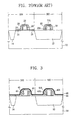
- FIGS. 1 and 2 are sectional views formation of silicide wiring in a conventional semiconductor device.
- a device separation region 14 and a wire separation region 12 are formed in a trench isolation process.
- the trenches are filled with a dielectric material according to standard practices.
- the device separation region 14 is provided in order to isolate separate respective devices, and the wire separation region 12 isolates respective wires.
- ion implantation of a device channel is performed, and the top of the resultant structure is coated with polysilicon to form a polysilicon 22 gate structure that is pattered via a photo etching process.
- appropriate ion implantation is performed.
- a gate spacer 20 is then formed, and a deep source/drain ion implantation is performed.
- material of Co, Ti or Ni etc. 24 is deposited, and then material nonreactive to a silicidation, such as TiN is deposited 26 .
- silicide reaction is performed in a thermal process, to thus form silicide films 16 , 18 , 28 in the device region 100 and the wiring region 200 .
- silicide films 16 , 18 are formed on regions where source and drain of a transistor will be formed, and silicide film 28 is formed on a gate electrode 22 .
- a silicide film 28 is formed on structure 22 A, which serves as a wire.
- the semiconductor process continues to strive toward gate lengths of ever-decreasing size, and, as a result, gate thickness also continues to decrease.
- the thickness of the silicide for reducing gate resistance becomes thinner while the junction depth becomes shallower. Consequently, the wiring resistance of the gate poly is increased and the operating speed of the resulting device is therefore reduced due to increased RC delay.
- Another object of the present invention is to provide a method of forming silicide wires in a semiconductor device, in which performance can be improved by reduction of resistance between a drain and source by using two transistors including a gate poly having mutually different thicknesses and a silicide layer having mutually different thicknesses, in the event that transistors are required that exhibit different input/output voltages and internal operating voltages.
- the present invention is directed to a method of forming silicide contacts in a semiconductor device.
- a gate film and a gate spacer are formed on a substrate in a device region and a wiring region of the substrate.
- a first metal film reactive to silicide and a reactive barrier film are sequentially formed on the resultant structure.
- Photoresist is deposited on the device region, the reactive barrier film of the wiring region is therefore exposed.
- the exposed reactive barrier film is removed and, the photoresist is removed.
- a second metal film reactive to the silicide is formed on the resultant structure.
- a silicide reaction is performed on the resultant structure, thereby providing a first silicide film formed on the gate film of the wiring region that is greater in thickness than a second silicide film formed on the gate film of the device region.
- the reactive barrier film may comprise, for example, TiN.
- the first and second metal films may comprise, for example, Co, Ti, or Ni
- the reacting and non-reacting residuals are removed in a cleaning process after performing the silicide reaction.
- the silicide reaction may comprise a rapid thermal process.
- the reactive barrier film is exposed by eliminating the photoresist formed on the wiring region while retaining the photoresist formed on the device region, through a photolithography process.
- the gate film of the wiring region may comprise, for example, an interconnect wire, or a transistor gate.
- the present invention is directed to a method of forming silicide wires in a semiconductor device.
- a gate film and a gate spacer are formed on a substrate in a device region and a wiring region of the substrate.
- a first metal film reactive to silicide and a reactive barrier film on the resultant structure are sequentially formed.
- Photoresist is deposited on the reactive barrier film.
- the photoresist formed on the wiring region is then removed so as to expose the reactive barrier film in the wiring region.
- the exposed reactive barrier film is removed and the photoresist in the device region is removed.
- a second metal film reactive to silicide on the resultant structure is formed after removing the photoresist in the device region.
- a silicide reaction is performed on the resultant structure, thereby providing a first silicide film formed on the gate film of the wiring region that is greater in thickness that a second silicide film formed on the gate film of the device region.
- FIGS. 1 and 2 represent sectional views in forming silicide wires in a conventional semiconductor device
- FIGS. 3 through 7 set forth sectional views in forming silicide wires in a semiconductor device in accordance with the preferred embodiment of the present invention.
- FIGS. 3 through 7 are sectional views showing a fabricating process for forming silicide wires in a semiconductor device in accordance with an embodiment of the present invention.
- a semiconductor substrate 30 comprises a device region 300 including respective devices and a wiring region 400 including wires, or interconnects.
- the device region 300 includes a device separation region 34 for isolating respective devices.
- the wiring region 400 includes a wire separation region 32 to provide for separation of wires.
- These device separation region 34 and wire separation region 32 are formed, for example, by a standard trench process in the semiconductor substrate 30 . Following trench formation, the trenches are filled with dielectric material, e.g., oxide. Following this, an ion implantation process of the channel is performed. The top of the resulting structure is coated with a polysilicon layer.
- the polysilicon layer is patterned, for example using photo etching, to form a transistor gate 42 in the device region and a wire pattern 42 A in the wiring region.
- an appropriate ion procedure is executed to form source and drain regions of the device.
- a deep source/drain ion implantation is performed.
- the entire surface of the resulting structure is deposited with a first metal film 44 reactive to silicide, for example comprising Co, Ti or Ni.
- a reactive barrier film 46 is deposited.
- the reactive barrier film 46 comprises a material nonreactive to silicidation, such as TiN.
- a layer of photoresist is deposited on the resultant structure.
- the photoresist is removed from the wiring region 400 using a photo etching process, to expose the portion of the reactive barrier film 46 deposited on the wiring region 400 .
- the photoresist 48 remains only in the device region 300 .
- the reactive barrier film 46 is removed in the exposed wiring region 400 is removed.
- the reactive barrier film 46 comprises, for example, TiN
- the reactive barrier film 46 is removed in a wet etching process using H 2 O 2 having high selectivity to cobalt.
- a second metal film 50 reactive to silicide for example comprising Co, Ti or Ni, is deposited on the surface of the resulting structure.
- a silicide reaction is performed, for example by rapid thermal processing (RTP), in the device region 300 and the wiring region 400 , so as to form a silicide film.
- RTP rapid thermal processing
- residue from the silicide reaction for example any nonreactive metal film and nonreactive barrier film 46 , are removed in a cleaning process.
- Silicide films 36 , 38 , 52 , 54 are then formed within the device region 300 and the wiring region 400 as shown in FIG. 7 .
- silicide films 36 and 38 are formed on regions corresponding to the transistor source and drain, while silicide film 52 is formed on the gate electrode 42 .
- silicide film 54 is formed on the polysilicon patter 42 A that comprises the wiring structure.
- the silicide film formed in the device region 300 has a layered structure composed of the first metal film 44 , the reactive barrier film 46 and the second metal film 50 .
- the reactive barrier film 46 thus remains between the first and second silicide-reactive metal films 44 , 50 .
- only the first metal film 44 reactive to the silicide reacts with the polysilicon gate pattern 42 so as to form the silicide film 52 .
- the first and second silicide-reactive metal films 44 , 50 both react with the polysilicon pattern 42 A so as to form the silicide film 54 . Since both metal layers 44 , 50 react in the wiring. region 400 , the resulting thickness of the silicide film 54 formed on the polysilicon wire pattern 42 A is, for example, on the order of twice the thickness of the silicide film 52 formed on the gate pattern 42 of the device region 300 . Accordingly, the operating speed of the semiconductor device is improved by reducing wiring resistance, since the thickness of the silicide film 54 on the wire pattern 42 A is increased.
- a silicide film formed on a wire pattern in the wiring region is formed to a greater thickness than a silicide film formed on a gate pattern in the device region, so as to reduce a wiring resistance. Accordingly, the operating speed of an integrated circuit composed of a large number of transistors can be improved.
- the process of the present invention can be applied to the case where multiple transistors of different silicide film thicknesses are required.
- the wire region 400 may comprise a second device region having a second gate pattern 42 A, rather than a wiring pattern. This is especially applicable to an embodiment requiring a difference between I/O voltage and internal operating voltage; therefore, gate poly layers of mutually different thicknesses and silicide layers of mutually different thicknesses are used so as to improve the performance of the device resulting from a reduction in the resistance between the source and drain.
Abstract
In an apparatus and method for forming a silicide wire in a semiconductor device, a first gate film is provided with a first silicide layer in a first region (for example a wiring region of the device that is relatively thicker than a second silicide layer on a second gate film in a second region of the device. In this manner, the operating speed of the semiconductor device is improved.
Description
1. Field of the Invention
The present invention relates to a method of forming wires in a semiconductor device; and more particularly, to a method of forming silicide wires in a semiconductor device, in which operating speed can be improved by increasing the thickness of the silicide wire.
2. Description of the Related Art
Silicide films are commonly applied in semiconductor devices for reducing contact resistance with polysilicon materials, for example polysilicon materials found in source and drain regions of a device The use of cobalt silicide film has recently become popular for this purpose. It is preferable to form the cobalt silicide film in a bi-layer system composed of a silicon surface and a cobalt film, wherein the silicon surface has a crystal structure that is compatible with the cobalt silicide film. Further, the cobalt film is formed by an initial deposition of a capping layer made of Ti, TiW or TiN prior to cobalt reaction. The capping layer improves the electrical characteristics of the device and mitigates excessive oxidation of the cobalt. An example of a Ti capping layer is disclosed in U.S. Pat. No. 5,736,461, illustrating a process for preventing cobalt oxidation during silicide formation.
In a typical cobalt silicide film process, the cobalt silicide film of uniform thickness is formed on a source region, a drain region, and a polysilicon gate region of a semiconductor device. Since the thickness of the silicide film plays an important role in the performance of the resulting semiconductor device, two separate semiconductor devices having mutually different junction depths between source and drain regions can be provided in a single integrated circuit. In other words, in a semiconductor device having a relatively shallow source and drain junction depth it is required to form a comparatively shallow cobalt silicide film on the source and drain regions in order to reduce the risk of a “spiking” phenomenon. In a semiconductor device having a relatively deep junction depth it is required to form a comparatively thick cobalt silicide film on regions having the deep junction depth in order to reduce contact resistance.
FIGS. 1 and 2 are sectional views formation of silicide wiring in a conventional semiconductor device.
With reference to FIG. 1, in a semiconductor substrate 10, a device separation region 14 and a wire separation region 12 are formed in a trench isolation process. The trenches are filled with a dielectric material according to standard practices. The device separation region 14 is provided in order to isolate separate respective devices, and the wire separation region 12 isolates respective wires. Subsequently, ion implantation of a device channel is performed, and the top of the resultant structure is coated with polysilicon to form a polysilicon 22 gate structure that is pattered via a photo etching process. Next, appropriate ion implantation is performed. A gate spacer 20 is then formed, and a deep source/drain ion implantation is performed. On the resultant structure, material of Co, Ti or Ni etc. 24 is deposited, and then material nonreactive to a silicidation, such as TiN is deposited 26.
With reference to FIG. 2, following this, silicide reaction is performed in a thermal process, to thus form silicide films 16, 18, 28 in the device region 100 and the wiring region 200. At this time, in the device region 100, silicide films 16, 18 are formed on regions where source and drain of a transistor will be formed, and silicide film 28 is formed on a gate electrode 22. In the wiring region 200, a silicide film 28 is formed on structure 22A, which serves as a wire.
In the conventional wiring method, the semiconductor process continues to strive toward gate lengths of ever-decreasing size, and, as a result, gate thickness also continues to decrease. As a result, the thickness of the silicide for reducing gate resistance becomes thinner while the junction depth becomes shallower. Consequently, the wiring resistance of the gate poly is increased and the operating speed of the resulting device is therefore reduced due to increased RC delay.
It is therefore an object of the present invention to provide a method of forming silicide wires in a semiconductor device, in which a wiring resistance can be reduced and in which operating speed can be improved by thickening the gate silicide for a gate structure that is used as a wire in the semiconductor device.
Another object of the present invention is to provide a method of forming silicide wires in a semiconductor device, in which performance can be improved by reduction of resistance between a drain and source by using two transistors including a gate poly having mutually different thicknesses and a silicide layer having mutually different thicknesses, in the event that transistors are required that exhibit different input/output voltages and internal operating voltages.
In one aspect, the present invention is directed to a method of forming silicide contacts in a semiconductor device. A gate film and a gate spacer are formed on a substrate in a device region and a wiring region of the substrate. A first metal film reactive to silicide and a reactive barrier film are sequentially formed on the resultant structure. Photoresist is deposited on the device region, the reactive barrier film of the wiring region is therefore exposed. The exposed reactive barrier film is removed and, the photoresist is removed. A second metal film reactive to the silicide is formed on the resultant structure. A silicide reaction is performed on the resultant structure, thereby providing a first silicide film formed on the gate film of the wiring region that is greater in thickness than a second silicide film formed on the gate film of the device region.
The reactive barrier film may comprise, for example, TiN. The first and second metal films may comprise, for example, Co, Ti, or Ni
In an optional embodiment, the reacting and non-reacting residuals are removed in a cleaning process after performing the silicide reaction. The silicide reaction may comprise a rapid thermal process.
The reactive barrier film is exposed by eliminating the photoresist formed on the wiring region while retaining the photoresist formed on the device region, through a photolithography process.
The gate film of the wiring region may comprise, for example, an interconnect wire, or a transistor gate.
In another aspect, the present invention is directed to a method of forming silicide wires in a semiconductor device. A gate film and a gate spacer are formed on a substrate in a device region and a wiring region of the substrate. A first metal film reactive to silicide and a reactive barrier film on the resultant structure are sequentially formed. Photoresist is deposited on the reactive barrier film. The photoresist formed on the wiring region is then removed so as to expose the reactive barrier film in the wiring region. The exposed reactive barrier film is removed and the photoresist in the device region is removed. A second metal film reactive to silicide on the resultant structure is formed after removing the photoresist in the device region. A silicide reaction is performed on the resultant structure, thereby providing a first silicide film formed on the gate film of the wiring region that is greater in thickness that a second silicide film formed on the gate film of the device region.
The above and other objects and features of the instant invention will become apparent from the following description of preferred embodiments taken in conjunction with the accompanying drawings, in which:
FIGS. 1 and 2 represent sectional views in forming silicide wires in a conventional semiconductor device; and
FIGS. 3 through 7 set forth sectional views in forming silicide wires in a semiconductor device in accordance with the preferred embodiment of the present invention.
Hereinafter, preferred embodiments of the present invention will be described in detail with reference to the accompanying drawings. Like reference numerals refer to like components throughout the drawings.
FIGS. 3 through 7 are sectional views showing a fabricating process for forming silicide wires in a semiconductor device in accordance with an embodiment of the present invention.
In FIG. 3, a semiconductor substrate 30 comprises a device region 300 including respective devices and a wiring region 400 including wires, or interconnects. The device region 300 includes a device separation region 34 for isolating respective devices. The wiring region 400 includes a wire separation region 32 to provide for separation of wires. These device separation region 34 and wire separation region 32 are formed, for example, by a standard trench process in the semiconductor substrate 30. Following trench formation, the trenches are filled with dielectric material, e.g., oxide. Following this, an ion implantation process of the channel is performed. The top of the resulting structure is coated with a polysilicon layer. The polysilicon layer is patterned, for example using photo etching, to form a transistor gate 42 in the device region and a wire pattern 42A in the wiring region. Next, an appropriate ion procedure is executed to form source and drain regions of the device. After forming a gate spacer 40, and wire pattern spacer 40A, a deep source/drain ion implantation is performed. The entire surface of the resulting structure is deposited with a first metal film 44 reactive to silicide, for example comprising Co, Ti or Ni. Next, a reactive barrier film 46 is deposited. The reactive barrier film 46 comprises a material nonreactive to silicidation, such as TiN.
Next, with reference to FIG. 4, a layer of photoresist is deposited on the resultant structure. The photoresist is removed from the wiring region 400 using a photo etching process, to expose the portion of the reactive barrier film 46 deposited on the wiring region 400. Thus the photoresist 48 remains only in the device region 300.
As shown in FIG. 5, the reactive barrier film 46 is removed in the exposed wiring region 400 is removed. Assuming the reactive barrier film 46 comprises, for example, TiN, the reactive barrier film 46 is removed in a wet etching process using H2O2 having high selectivity to cobalt.
As shown in FIG. 6, after removing the photoresist 48 deposited on the device region 300 by the photo etching process, a second metal film 50 reactive to silicide, for example comprising Co, Ti or Ni, is deposited on the surface of the resulting structure. Subsequently, a silicide reaction is performed, for example by rapid thermal processing (RTP), in the device region 300 and the wiring region 400, so as to form a silicide film. After forming the silicide film, residue from the silicide reaction, for example any nonreactive metal film and nonreactive barrier film 46, are removed in a cleaning process. Silicide films 36, 38, 52, 54 are then formed within the device region 300 and the wiring region 400 as shown in FIG. 7.
At this time, in the device region 300, silicide films 36 and 38 are formed on regions corresponding to the transistor source and drain, while silicide film 52 is formed on the gate electrode 42. In the wiring region 400, silicide film 54 is formed on the polysilicon patter 42A that comprises the wiring structure.
With reference to FIGS. 6 and 7, the silicide film formed in the device region 300 has a layered structure composed of the first metal film 44, the reactive barrier film 46 and the second metal film 50. The reactive barrier film 46 thus remains between the first and second silicide- reactive metal films 44, 50. Thus, in the device region 300, only the first metal film 44 reactive to the silicide reacts with the polysilicon gate pattern 42 so as to form the silicide film 52.
In the wiring region 400 however, owing to the absence of the barrier layer, the first and second silicide- reactive metal films 44, 50 both react with the polysilicon pattern 42A so as to form the silicide film 54. Since both metal layers 44, 50 react in the wiring. region 400, the resulting thickness of the silicide film 54 formed on the polysilicon wire pattern 42A is, for example, on the order of twice the thickness of the silicide film 52 formed on the gate pattern 42 of the device region 300. Accordingly, the operating speed of the semiconductor device is improved by reducing wiring resistance, since the thickness of the silicide film 54 on the wire pattern 42A is increased.
As described above, in accordance with the present invention, in fabricating a semiconductor memory device, a silicide film formed on a wire pattern in the wiring region is formed to a greater thickness than a silicide film formed on a gate pattern in the device region, so as to reduce a wiring resistance. Accordingly, the operating speed of an integrated circuit composed of a large number of transistors can be improved.
Further, the process of the present invention can be applied to the case where multiple transistors of different silicide film thicknesses are required. In this embodiment, the wire region 400 may comprise a second device region having a second gate pattern 42A, rather than a wiring pattern. This is especially applicable to an embodiment requiring a difference between I/O voltage and internal operating voltage; therefore, gate poly layers of mutually different thicknesses and silicide layers of mutually different thicknesses are used so as to improve the performance of the device resulting from a reduction in the resistance between the source and drain.
While this invention has been particularly described with reference to preferred embodiments thereof, it will be understood by those skilled in the art that various changes in form and details may be made therein without departing from the spirit and scope of the invention as defined by the appended claims.
Claims (18)
1. A method of forming silicide contacts in a semiconductor device, comprising the steps of:
forming a gate film and a gate spacer on a substrate in a device region and a wiring region of the substrate;
sequentially forming a first metal film reactive to silicide and a reactive barrier film on the resultant structure;
depositing photoresist on the device region, and exposing the reactive barrier film of the wiring region;
removing the exposed reactive barrier film, removing the photoresist, and forming a second metal film reactive to the silicide on the resultant structure; and
performing a silicide reaction on the resultant structure, thereby providing a first silicide film formed on the gate film of the wiring region that is greater in thickness than a second silicide film formed on the gate film of the device region.
2. The method of claim 1 , wherein said reactive barrier film comprises TiN.
3. The method of claim 1 , wherein said first and second metal films comprise Co.
4. The method of claim 1 , wherein said first and second metal films comprise Ti.
5. The method of claim 1 , wherein said first and second metal films comprise Ni.
6. The method of claim 1 , further comprising the step of removing reacting and non-reacting residuals in a cleaning process after performing the silicide reaction.
7. The method of claim 1 , wherein said silicide reaction comprises a rapid thermal process.
8. The method of claim 1 , wherein said reactive barrier film is exposed by eliminating the photoresist formed on the wiring region while retaining the photoresist formed on the device region, through a photolithography process.
9. The method of claim 1 wherein the gate film of the wiring region comprises an interconnect wire.
10. The method of claim 1 wherein the gate film of the wiring region comprises a transistor gate.
11. A method of forming silicide wires in a semiconductor device, comprising the steps of:
forming a gate film and a gate spacer on a substrate in a device region and a wiring region of the substrate;
sequentially forming a first metal film reactive to silicide and a reactive barrier film on the resultant structure;
depositing photoresist on the reactive barrier film;
removing the photoresist formed on the wiring region so as to expose the reactive barrier film in the wiring region;
removing the exposed reactive barrier film, and removing the photoresist in the device region;
forming a second metal film reactive to silicide on the resultant structure after removing the photoresist in the device region; and
performing a silicide reaction on the resultant structure, thereby providing a first silicide film formed on the gate film of the wiring region that is greater in thickness that a second silicide film formed on the gate film of the device region.
12. The method of claim 11 , further comprising the step of removing reacting and non-reacting residuals in a cleaning process after performing the silicide reaction.
13. The method of claim 11 , wherein said reactive barrier film comprises TiN.
14. The method of claim 11 , wherein said first and second metal films comprise Co.
15. The method of claim 11 , wherein said first and second metal films comprise Ti.
16. The method of claim 11 , wherein said first and second metal films comprise Ni.
17. The method of claim 11 wherein the gate film of the wiring region comprises an interconnect wire.
18. The method of claim 11 wherein the gate film of the wiring region comprises a transistor gate.
Applications Claiming Priority (2)
| Application Number | Priority Date | Filing Date | Title |
|---|---|---|---|
| KR02-43843 | 2002-07-25 | ||
| KR10-2002-0043843A KR100465876B1 (en) | 2002-07-25 | 2002-07-25 | Method for forming silicide wires of semiconductor element |
Publications (2)
| Publication Number | Publication Date |
|---|---|
| US20040029348A1 US20040029348A1 (en) | 2004-02-12 |
| US6828236B2 true US6828236B2 (en) | 2004-12-07 |
Family
ID=31492778
Family Applications (1)
| Application Number | Title | Priority Date | Filing Date |
|---|---|---|---|
| US10/378,705 Expired - Lifetime US6828236B2 (en) | 2002-07-25 | 2003-03-04 | Method for forming silicide wires in a semiconductor device |
Country Status (2)
| Country | Link |
|---|---|
| US (1) | US6828236B2 (en) |
| KR (1) | KR100465876B1 (en) |
Cited By (2)
| Publication number | Priority date | Publication date | Assignee | Title |
|---|---|---|---|---|
| US20050042831A1 (en) * | 2003-08-19 | 2005-02-24 | Manoj Mehrotra | Dual salicide process for optimum performance |
| US7112529B2 (en) * | 2004-04-09 | 2006-09-26 | Magnachip Semiconductor, Ltd. | Method of improving residue and thermal characteristics of semiconductor device |
Families Citing this family (4)
| Publication number | Priority date | Publication date | Assignee | Title |
|---|---|---|---|---|
| JP4398829B2 (en) * | 2004-09-17 | 2010-01-13 | 株式会社東芝 | Semiconductor device |
| KR100642648B1 (en) * | 2005-09-13 | 2006-11-10 | 삼성전자주식회사 | Contact structure having silicide layers, semiconductor device employing the same, and methods of fabricating the same |
| US20070123042A1 (en) * | 2005-11-28 | 2007-05-31 | International Business Machines Corporation | Methods to form heterogeneous silicides/germanides in cmos technology |
| DE102006046376B4 (en) * | 2006-09-29 | 2011-03-03 | Advanced Micro Devices, Inc., Sunnyvale | A method of fabricating field effect transistors having a technique for locally adjusting transistor characteristics by using advanced laser / flashlamping techniques suitable also for the fabrication of transistor elements of SRAM cells |
Citations (11)
| Publication number | Priority date | Publication date | Assignee | Title |
|---|---|---|---|---|
| US5387535A (en) * | 1992-06-15 | 1995-02-07 | Deutsche Itt Industries Gmbh | Method of fabricating semiconductor devices in CMOS technology with local interconnects |
| US5736461A (en) | 1992-03-02 | 1998-04-07 | Digital Equipment Corporation | Self-aligned cobalt silicide on MOS integrated circuits |
| US5889331A (en) * | 1996-12-31 | 1999-03-30 | Intel Corporation | Silicide for achieving low sheet resistance on poly-Si and low Si consumption in source/drain |
| US5891785A (en) * | 1997-01-15 | 1999-04-06 | Winbond Electronics Corp. | Process for forming self-aligned silicide |
| US5902129A (en) | 1997-04-07 | 1999-05-11 | Lsi Logic Corporation | Process for forming improved cobalt silicide layer on integrated circuit structure using two capping layers |
| US5911114A (en) * | 1997-03-21 | 1999-06-08 | National Semiconductor Corporation | Method of simultaneous formation of salicide and local interconnects in an integrated circuit structure |
| US6180469B1 (en) * | 1998-11-06 | 2001-01-30 | Advanced Micro Devices, Inc. | Low resistance salicide technology with reduced silicon consumption |
| US6329276B1 (en) | 1998-12-01 | 2001-12-11 | Samsung Electronics Co. Ltd. | Method of forming self-aligned silicide in semiconductor device |
| US6514859B1 (en) * | 2000-12-08 | 2003-02-04 | Advanced Micro Devices, Inc. | Method of salicide formation with a double gate silicide |
| US6521528B1 (en) * | 1996-06-26 | 2003-02-18 | Kabushiki Kaisha Toshiba | Semiconductor device and method of making thereof |
| US6673665B2 (en) * | 2002-02-28 | 2004-01-06 | Advanced Micro Devices, Inc. | Semiconductor device having increased metal silicide portions and method of forming the semiconductor |
Family Cites Families (2)
| Publication number | Priority date | Publication date | Assignee | Title |
|---|---|---|---|---|
| US6040606A (en) * | 1998-11-04 | 2000-03-21 | National Semiconductor Corporation | Integrated circuit structure with dual thickness cobalt silicide layers and method for its manufacture |
| JP2000332220A (en) * | 1999-05-25 | 2000-11-30 | Sony Corp | Semiconductor device and manufacture thereof |
-
2002
- 2002-07-25 KR KR10-2002-0043843A patent/KR100465876B1/en active IP Right Grant
-
2003
- 2003-03-04 US US10/378,705 patent/US6828236B2/en not_active Expired - Lifetime
Patent Citations (11)
| Publication number | Priority date | Publication date | Assignee | Title |
|---|---|---|---|---|
| US5736461A (en) | 1992-03-02 | 1998-04-07 | Digital Equipment Corporation | Self-aligned cobalt silicide on MOS integrated circuits |
| US5387535A (en) * | 1992-06-15 | 1995-02-07 | Deutsche Itt Industries Gmbh | Method of fabricating semiconductor devices in CMOS technology with local interconnects |
| US6521528B1 (en) * | 1996-06-26 | 2003-02-18 | Kabushiki Kaisha Toshiba | Semiconductor device and method of making thereof |
| US5889331A (en) * | 1996-12-31 | 1999-03-30 | Intel Corporation | Silicide for achieving low sheet resistance on poly-Si and low Si consumption in source/drain |
| US5891785A (en) * | 1997-01-15 | 1999-04-06 | Winbond Electronics Corp. | Process for forming self-aligned silicide |
| US5911114A (en) * | 1997-03-21 | 1999-06-08 | National Semiconductor Corporation | Method of simultaneous formation of salicide and local interconnects in an integrated circuit structure |
| US5902129A (en) | 1997-04-07 | 1999-05-11 | Lsi Logic Corporation | Process for forming improved cobalt silicide layer on integrated circuit structure using two capping layers |
| US6180469B1 (en) * | 1998-11-06 | 2001-01-30 | Advanced Micro Devices, Inc. | Low resistance salicide technology with reduced silicon consumption |
| US6329276B1 (en) | 1998-12-01 | 2001-12-11 | Samsung Electronics Co. Ltd. | Method of forming self-aligned silicide in semiconductor device |
| US6514859B1 (en) * | 2000-12-08 | 2003-02-04 | Advanced Micro Devices, Inc. | Method of salicide formation with a double gate silicide |
| US6673665B2 (en) * | 2002-02-28 | 2004-01-06 | Advanced Micro Devices, Inc. | Semiconductor device having increased metal silicide portions and method of forming the semiconductor |
Cited By (3)
| Publication number | Priority date | Publication date | Assignee | Title |
|---|---|---|---|---|
| US20050042831A1 (en) * | 2003-08-19 | 2005-02-24 | Manoj Mehrotra | Dual salicide process for optimum performance |
| US6987061B2 (en) * | 2003-08-19 | 2006-01-17 | Texas Instruments Incorporated | Dual salicide process for optimum performance |
| US7112529B2 (en) * | 2004-04-09 | 2006-09-26 | Magnachip Semiconductor, Ltd. | Method of improving residue and thermal characteristics of semiconductor device |
Also Published As
| Publication number | Publication date |
|---|---|
| US20040029348A1 (en) | 2004-02-12 |
| KR100465876B1 (en) | 2005-01-13 |
| KR20040009785A (en) | 2004-01-31 |
Similar Documents
| Publication | Publication Date | Title |
|---|---|---|
| US7759202B2 (en) | Method for forming semiconductor device with gates of different materials | |
| JP4767946B2 (en) | Complementary metal oxide semiconductor integrated circuit with NMOS and PMOS transistors using different gate dielectrics | |
| US6103610A (en) | Integrated circuit structure with dual thickness cobalt silicide layers and method for its manufacture | |
| US8658487B2 (en) | Semiconductor device and fabrication method thereof | |
| US5573980A (en) | Method of forming salicided self-aligned contact for SRAM cells | |
| US7186605B2 (en) | Method of fabricating gates | |
| US20090035902A1 (en) | Integrated method of fabricating a memory device with reduced pitch | |
| US6794252B2 (en) | Method and system for forming dual work function gate electrodes in a semiconductor device | |
| US7622347B2 (en) | Self-aligned metal electrode to eliminate native oxide effect for metal insulator semiconductor (MIS) capacitor | |
| JP2004140262A (en) | Semiconductor device and manufacturing method thereof | |
| US6288430B1 (en) | Semiconductor device having silicide layer with siliconrich region and method for making the same | |
| US6828236B2 (en) | Method for forming silicide wires in a semiconductor device | |
| US6352899B1 (en) | Raised silicide source/drain MOS transistors having enlarged source/drain contact regions and method | |
| US7432147B2 (en) | Method of manufacturing semiconductor device | |
| JP2001093888A (en) | Method for manufacturing semiconductor device | |
| US8877577B2 (en) | Semiconductor device and manufacturing method thereof | |
| US20010045661A1 (en) | Composite metallization process for filling high aspect ratio contact holes | |
| JP2008021935A (en) | Electronic device and manufacturing method thereof | |
| JPH08321591A (en) | Semiconductor device and fabrication thereof | |
| US20060246685A1 (en) | Semiconductor device fabrication method | |
| US7045422B2 (en) | Semiconductor gate structure and method for fabricating a semiconductor gate structure | |
| WO2016169202A1 (en) | Method for manufacture of array substrate, array substrate, and display device | |
| KR950011554B1 (en) | Multi-layer metalizing method of semiconductor device | |
| US20070202688A1 (en) | Method for forming contact opening | |
| KR100564432B1 (en) | Method for manufacturing Transistor |
Legal Events
| Date | Code | Title | Description |
|---|---|---|---|
| AS | Assignment |
Owner name: SAMSUNG ELECTRONICS, CO., LTD., KOREA, REPUBLIC OF Free format text: ASSIGNMENT OF ASSIGNORS INTEREST;ASSIGNOR:LEE, DONG-HUN;REEL/FRAME:013854/0719 Effective date: 20030221 |
|
| STCF | Information on status: patent grant |
Free format text: PATENTED CASE |
|
| FEPP | Fee payment procedure |
Free format text: PAYOR NUMBER ASSIGNED (ORIGINAL EVENT CODE: ASPN); ENTITY STATUS OF PATENT OWNER: LARGE ENTITY |
|
| FPAY | Fee payment |
Year of fee payment: 4 |
|
| FPAY | Fee payment |
Year of fee payment: 8 |
|
| FPAY | Fee payment |
Year of fee payment: 12 |