US6806580B2 - Multichip module including substrate with an array of interconnect structures - Google Patents
Multichip module including substrate with an array of interconnect structures Download PDFInfo
- Publication number
- US6806580B2 US6806580B2 US10/330,741 US33074102A US6806580B2 US 6806580 B2 US6806580 B2 US 6806580B2 US 33074102 A US33074102 A US 33074102A US 6806580 B2 US6806580 B2 US 6806580B2
- Authority
- US
- United States
- Prior art keywords
- multichip module
- substrate
- semiconductor die
- vertical transistor
- semiconductor
- Prior art date
- Legal status (The legal status is an assumption and is not a legal conclusion. Google has not performed a legal analysis and makes no representation as to the accuracy of the status listed.)
- Expired - Lifetime, expires
Links
- 239000000758 substrate Substances 0.000 title claims abstract description 64
- 239000004065 semiconductor Substances 0.000 claims abstract description 82
- 238000004891 communication Methods 0.000 claims abstract description 9
- 229910000679 solder Inorganic materials 0.000 claims description 39
- 239000000919 ceramic Substances 0.000 claims description 14
- 230000001360 synchronised effect Effects 0.000 claims description 9
- PNEYBMLMFCGWSK-UHFFFAOYSA-N aluminium oxide Inorganic materials [O-2].[O-2].[O-2].[Al+3].[Al+3] PNEYBMLMFCGWSK-UHFFFAOYSA-N 0.000 claims description 3
- 230000002093 peripheral effect Effects 0.000 claims description 3
- 239000002356 single layer Substances 0.000 claims 3
- 238000000034 method Methods 0.000 description 12
- 238000010586 diagram Methods 0.000 description 4
- 239000000463 material Substances 0.000 description 4
- RYGMFSIKBFXOCR-UHFFFAOYSA-N Copper Chemical compound [Cu] RYGMFSIKBFXOCR-UHFFFAOYSA-N 0.000 description 3
- 229910052802 copper Inorganic materials 0.000 description 3
- 239000010949 copper Substances 0.000 description 3
- 230000007423 decrease Effects 0.000 description 3
- 241001133184 Colletotrichum agaves Species 0.000 description 2
- 239000003990 capacitor Substances 0.000 description 2
- 150000001875 compounds Chemical class 0.000 description 2
- 230000005669 field effect Effects 0.000 description 2
- 230000014509 gene expression Effects 0.000 description 2
- 230000017525 heat dissipation Effects 0.000 description 2
- 239000012778 molding material Substances 0.000 description 2
- 238000000465 moulding Methods 0.000 description 2
- 238000007639 printing Methods 0.000 description 2
- 229910020220 Pb—Sn Inorganic materials 0.000 description 1
- 229910045601 alloy Inorganic materials 0.000 description 1
- 239000000956 alloy Substances 0.000 description 1
- 229910052782 aluminium Inorganic materials 0.000 description 1
- XAGFODPZIPBFFR-UHFFFAOYSA-N aluminium Chemical compound [Al] XAGFODPZIPBFFR-UHFFFAOYSA-N 0.000 description 1
- 230000000295 complement effect Effects 0.000 description 1
- 238000000151 deposition Methods 0.000 description 1
- 230000008021 deposition Effects 0.000 description 1
- 238000009792 diffusion process Methods 0.000 description 1
- 230000009977 dual effect Effects 0.000 description 1
- 230000000694 effects Effects 0.000 description 1
- 238000009713 electroplating Methods 0.000 description 1
- 238000005516 engineering process Methods 0.000 description 1
- 229910052751 metal Inorganic materials 0.000 description 1
- 239000002184 metal Substances 0.000 description 1
- 229910044991 metal oxide Inorganic materials 0.000 description 1
- 150000004706 metal oxides Chemical class 0.000 description 1
- 238000001465 metallisation Methods 0.000 description 1
- 238000012986 modification Methods 0.000 description 1
- 230000004048 modification Effects 0.000 description 1
- 238000005457 optimization Methods 0.000 description 1
- 238000004806 packaging method and process Methods 0.000 description 1
- 238000000206 photolithography Methods 0.000 description 1
- 239000003870 refractory metal Substances 0.000 description 1
- 238000004544 sputter deposition Methods 0.000 description 1
Images


Classifications
-
- H—ELECTRICITY
- H05—ELECTRIC TECHNIQUES NOT OTHERWISE PROVIDED FOR
- H05K—PRINTED CIRCUITS; CASINGS OR CONSTRUCTIONAL DETAILS OF ELECTRIC APPARATUS; MANUFACTURE OF ASSEMBLAGES OF ELECTRICAL COMPONENTS
- H05K1/00—Printed circuits
- H05K1/02—Details
- H05K1/14—Structural association of two or more printed circuits
- H05K1/141—One or more single auxiliary printed circuits mounted on a main printed circuit, e.g. modules, adapters
-
- H—ELECTRICITY
- H01—ELECTRIC ELEMENTS
- H01L—SEMICONDUCTOR DEVICES NOT COVERED BY CLASS H10
- H01L2924/00—Indexing scheme for arrangements or methods for connecting or disconnecting semiconductor or solid-state bodies as covered by H01L24/00
- H01L2924/0001—Technical content checked by a classifier
- H01L2924/0002—Not covered by any one of groups H01L24/00, H01L24/00 and H01L2224/00
-
- H—ELECTRICITY
- H05—ELECTRIC TECHNIQUES NOT OTHERWISE PROVIDED FOR
- H05K—PRINTED CIRCUITS; CASINGS OR CONSTRUCTIONAL DETAILS OF ELECTRIC APPARATUS; MANUFACTURE OF ASSEMBLAGES OF ELECTRICAL COMPONENTS
- H05K1/00—Printed circuits
- H05K1/02—Details
- H05K1/03—Use of materials for the substrate
- H05K1/0306—Inorganic insulating substrates, e.g. ceramic, glass
-
- H—ELECTRICITY
- H05—ELECTRIC TECHNIQUES NOT OTHERWISE PROVIDED FOR
- H05K—PRINTED CIRCUITS; CASINGS OR CONSTRUCTIONAL DETAILS OF ELECTRIC APPARATUS; MANUFACTURE OF ASSEMBLAGES OF ELECTRICAL COMPONENTS
- H05K1/00—Printed circuits
- H05K1/18—Printed circuits structurally associated with non-printed electric components
- H05K1/181—Printed circuits structurally associated with non-printed electric components associated with surface mounted components
-
- H—ELECTRICITY
- H05—ELECTRIC TECHNIQUES NOT OTHERWISE PROVIDED FOR
- H05K—PRINTED CIRCUITS; CASINGS OR CONSTRUCTIONAL DETAILS OF ELECTRIC APPARATUS; MANUFACTURE OF ASSEMBLAGES OF ELECTRICAL COMPONENTS
- H05K2201/00—Indexing scheme relating to printed circuits covered by H05K1/00
- H05K2201/10—Details of components or other objects attached to or integrated in a printed circuit board
- H05K2201/10613—Details of electrical connections of non-printed components, e.g. special leads
- H05K2201/10621—Components characterised by their electrical contacts
- H05K2201/10689—Leaded Integrated Circuit [IC] package, e.g. dual-in-line [DIL]
-
- H—ELECTRICITY
- H05—ELECTRIC TECHNIQUES NOT OTHERWISE PROVIDED FOR
- H05K—PRINTED CIRCUITS; CASINGS OR CONSTRUCTIONAL DETAILS OF ELECTRIC APPARATUS; MANUFACTURE OF ASSEMBLAGES OF ELECTRICAL COMPONENTS
- H05K2203/00—Indexing scheme relating to apparatus or processes for manufacturing printed circuits covered by H05K3/00
- H05K2203/15—Position of the PCB during processing
- H05K2203/1572—Processing both sides of a PCB by the same process; Providing a similar arrangement of components on both sides; Making interlayer connections from two sides
-
- H—ELECTRICITY
- H05—ELECTRIC TECHNIQUES NOT OTHERWISE PROVIDED FOR
- H05K—PRINTED CIRCUITS; CASINGS OR CONSTRUCTIONAL DETAILS OF ELECTRIC APPARATUS; MANUFACTURE OF ASSEMBLAGES OF ELECTRICAL COMPONENTS
- H05K3/00—Apparatus or processes for manufacturing printed circuits
- H05K3/30—Assembling printed circuits with electric components, e.g. with resistor
- H05K3/32—Assembling printed circuits with electric components, e.g. with resistor electrically connecting electric components or wires to printed circuits
- H05K3/34—Assembling printed circuits with electric components, e.g. with resistor electrically connecting electric components or wires to printed circuits by soldering
- H05K3/341—Surface mounted components
- H05K3/3431—Leadless components
- H05K3/3436—Leadless components having an array of bottom contacts, e.g. pad grid array or ball grid array components
Definitions
- a semiconductor die package There are a number of semiconductor die packages.
- a semiconductor die is mounted to a lead frame with leads. Wires couple the semiconductor die to the leads. The wires, the semiconductor die and then the most of the lead frame (except for the leads that extend outward) are then encapsulated in a molding material. The molding material is then shaped.
- the formed semiconductor die package includes a molded body that has leads extending laterally away from the molded body. The semiconductor die package is then mounted onto a circuit board.
- Embodiments of the invention address these and other problems individually and collectively.
- Embodiments of the invention relate to multichip modules.
- the multichip modules may contain components that can form part of an electrical device such as a synchronous buck converter.
- the multichip module comprises: (a) a substrate having a first side and a second side, the second side being opposite the first side; (b) a chip at the first side of the substrate; (c) a semiconductor die comprising a vertical transistor at the second side, wherein the chip and the semiconductor die are in electrical communication through the substrate; and (d) an array of solder interconnect structures at the second side of the substrate.
- the multichip module comprises: (a) a ceramic substrate having a first side and a second side, the first side being opposite the first side; (b) a driver chip at the first side of the substrate; (c) a first semiconductor die comprising a first vertical transistor at the second side, wherein the driver chip and the first semiconductor die are in electrical communication through the ceramic substrate; (d) a second semiconductor die comprising a second vertical transistor at the second side, wherein the driver chip and the second semiconductor die are in electrical communication through the ceramic substrate; and (e) an array of solder interconnect structures disposed around the first and second semiconductor dies.
- FIG. 1 shows a top perspective view of a multichip module according to an embodiment of the invention.
- FIG. 2 shows a bottom perspective view of a multichip module according to an embodiment of the invention.
- FIG. 3 shows a top plan view of a multichip module according to an embodiment of the invention.
- FIG. 4 shows a side view of a multichip module according to an embodiment of the invention.
- FIG. 5 shows a front view of a multichip module according to an embodiment of the invention.
- FIG. 6 shows a bottom plan view of a multichip module according to an embodiment of the invention.
- FIG. 7 shows an exploded view of a multichip module according to an embodiment of the invention.
- FIG. 8 shows an electrical diagram for a synchronous buck converter application.
- Embodiments of the invention are directed to multichip modules.
- One embodiment of the invention is directed to a multichip module comprising a substrate having a first side and a second side, the second side being opposite the first side.
- a driver chip package comprising a driver chip is at the first side of the substrate.
- a semiconductor die comprising a vertical transistor is at the second side.
- the driver chip package and the semiconductor die are in electrical communication through the substrate.
- the substrate comprises a ceramic substrate (e.g., an alumina substrate) and an array of solder interconnect structures is formed at the second side of the substrate around the semiconductor die.
- the components in the multichip module may form part of any suitable electronic circuit.
- the components in the multichip modules according to embodiments of the invention can form part of a synchronous Buck converter.
- Synchronous Buck converters are used to step down an input voltage, and are described in further detail below.
- synchronous Buck converters are described in detail herein, it is understood that the multichip modules according to embodiments of the invention could be part of electronic circuits that do not include a synchronous Buck converter.
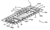
- FIG. 1 shows a top perspective view of a multichip module 100 according to an embodiment of the invention.
- the multichip module 100 includes a driver chip package 2 having a number of leads 2 ( a ), and is mounted on a first side 1 ( a ) of a substrate 1 .
- Solder such as Pb-Sn solder may be used to mechanically and electrically couple the leads 2 ( a ) of the driver chip package 2 to the substrate 1 .
- the solder that is used to couple the leads 2 ( a ) of the driver chip package 2 to the substrate 1 may be present on the conductive lands 4 .
- the driver chip package 2 is illustrated as being a leaded package. In other embodiments, the driver chip package could be a leadless chip package. Regardless of whether the driver chip package is leaded or leadless, suitable driver chip packages can be commercially obtained.
- suitable driver chip packages e.g., FAN 5003 drivers
- FAN 5003 drivers can be obtained from Fairchild Semiconductor, Inc. of Portland, Me.
- the conductive traces 3 and conductive lands 4 are at the first side 1 ( a ) of the substrate 1 .
- the conductive traces 3 and the conductive lands 4 can comprise any suitable material and can be made in any suitable manner.
- the conductive traces 3 and the conductive lands 4 can comprise a material such as copper, aluminum, refractory metals, and alloys thereof. They can be made using processes known to those skilled in the art.
- exemplary processes include metal deposition processes such as electroplating and sputtering that are used in conjunction with photolithography processes.
- FIG. 2 shows the multichip module 100 shown in FIG. 1 from a bottom perspective view.
- the substrate 1 has a second side 1 ( b ) that is opposite to the first side 1 ( a ).
- a first semiconductor die 7 and a second semiconductor die 8 are mounted to the second side 1 ( b ).
- the first semiconductor die 7 can include a first MOSFET including a first source region and a first gate region at a first side of the first semiconductor die 7 , and a first drain region at an opposite second side of the semiconductor die 7 .
- the second semiconductor die 8 can also include a second MOSFET including a second source region and a second gate region at a first side, and a second drain region at a second side of the second semiconductor die 8 .
- the first and second drain regions of the first and second semiconductor dies 7 , 8 would face away from the driver chip package 2 and would be mounted to a circuit board (not shown) using solder.
- embodiments of the invention have electronic components mounted on both sides of the substrate.
- the components can be “stacked” so that their density is maximized in the final multichip module. This increases the density of components while it also decreases the footprint of components on a circuit board.
- the first MOSFET in the first semiconductor die 7 can be a “low drive field effect transistor”, while the second MOSFET in the second semiconductor die 8 can be a “high drive filed effect transistor” in a synchronous Buck converter.
- a Buck topology is used to convert an input voltage to a lower output voltage.
- a synchronous Buck converter includes a pair of switching transistors coupled in series across the input voltage source, with a high side switch coupled to the input voltage and a low side switch coupled to ground. The switches are controlled to alternately conduct with complementary duty cycles to maintain a predetermined output voltage. In the embodiment shown in FIGS.
- the driver chip in the driver chip package 2 can be used to control the switching in the first and second MOSFETs in the first and second semiconductor dies 7 , 8 .
- An output filter (not shown in FIGS. 1 and 2 ), including an inductor and a capacitor, is coupled to the interconnection between the pair of switching transistors and averages the switched input voltage to provide the lower output voltage.
- Buck converters are known in the art. An exemplary circuit diagram for a Buck converter is shown in FIG. 8 of the present application. It includes a driver 200 that controls MOSFETs Q 1 and Q 2 .
- Other examples of Buck converters are described in U.S. Pat. Nos. 5,627,460, 6,222,352, and 6,166,528. All of these U.S. Patents are herein incorporated by reference in their entity.
- the transistors in the first and second semiconductor dies 7 , 8 can include vertical power transistors.
- Vertical power transistors include VDMOS transistors and vertical bipolar power transistors.
- a VDMOS transistor is a MOSFET (metal oxide semiconductor field effect transistor) that has two or more semiconductor regions formed by diffusion. It has a source region, a drain region, and a gate. The device is vertical in that the source region and the drain region are at opposite surfaces of the semiconductor die.
- the gate may be a trenched gate structure or a planar gate structure, and is formed at the same surface as the source region. During operation, the current flow from the source region to the drain region in a VDMOS device is substantially perpendicular to the die surfaces.
- the transistors in the semiconductor dies can be bipolar transistors. In such embodiments, one side of the semiconductor die can have an emitter region and a base region. The other side of the die can have a collector region.
- the first and the second semiconductor dies 7 , 8 can be mounted to the second side 1 ( b ) of the substrate 1 using first and second sets of solder joints 17 , 18 .
- the first set of solder joints 17 can include a first plurality of source solder joints 17 ( s ) coupled to a first source region of a first MOSFET in the first semiconductor die 7 , and a first gate solder joint 17 ( g ) coupled to a first gate region of a MOSFET in the first semiconductor die 7 .
- the second set of solder joints 18 can include a second plurality of source solder joints 18 ( s ) coupled to a second source region of a second MOSFET in the second semiconductor die 8 , and a gate solder joint 18 ( g ) coupled to a gate region of the second MOSFET.
- the drain regions of the first and second MOSFETs in the first and second semiconductor dies 7 , 8 would be distal to the substrate 1 while the source and the gate regions would be proximate to the substrate 1 .
- the drain regions of the first and second MOSFETs in the first and second semiconductor dies 7 , 8 are soldered to conductive pads on the circuit board.
- the second side 1 ( b ) of the substrate 1 can be metallized with conductive regions 9 such as conductive lines, conductive lands, etc.
- the conductive regions 9 can include the same or different materials, and/or can be made by the same or different method as the conductive traces 3 and conductive lands 4 on the first side 1 ( a ) of the substrate 1 .
- the substrate 1 has a bottom side conductive region 6 ( a ) that provides a source connection (e.g., a low side source connection) for the first semiconductor die 7 .
- the substrate 1 also has a bottom side conductive region 6 ( b ) that provides a source connection (e.g., a high side source connection) for the second semiconductor die 8 .
- an array of solder interconnect structures 10 (e.g., solder balls) is disposed around the first and second semiconductor dies 7 , 8 .
- the solder interconnect structures 10 can be at the periphery of the substrate 1 and can substantially completely surround the first and second semiconductor dies 7 , 8 .
- Some of the solder interconnect structures 10 are in communication the driver chip package 2 on the first side 1 ( a ) of the substrate through a number of conductive vias 5 that are also at the periphery of the substrate 1 .
- the array of solder interconnect structures 10 can be formed by any suitable method including solder paste printing, solder ball pick and place, etc. A subsequent reflow step can be performed to reflow the deposited solder. Solder deposition and reflow processes are known in the art.
- the first and second semiconductor dies 7 , 8 are unpackaged. Unpackaged semiconductor dies do not have a molding compound that encapsulates them. However, in other embodiments, the first and second semiconductor dies 7 , 8 , could be packaged with a molding compound, or with any other suitable material. If they are packaged, the resulting die packages may be leadless or leaded. Examples of packaged dies are described in U.S. Pat. Nos. 6,469,384 and 6,133,634, both by Rajeev Joshi, a co-inventor in the present application. These U.S. Patents are herein incorporated by reference.
- FIG. 3 shows a top, planar view the multichip module 100 .
- a number of abbreviations e.g., D 1 , S 1 , etc.
- These abbreviations correspond to the solder interconnect structures at the second side of the substrate 1 .
- the abbreviations are described below with reference to FIGS. 6 and 8.
- Reference numeral 101 shows a connection between a lead of the driver chip package 2 and gate region in the low side MOSFET in the first semiconductor die 7 .
- Reference numeral 103 shows a connection between a lead of the driver chip package 2 and the gate region of the high side MOSFET in the second semiconductor die 8 .
- Low drive signals pass through the circuit path shown by reference numeral 101 and high drive signals pass through the circuit path shown by reference numeral 103 .
- the interconnect path lengths between the driver chip package 2 and the MOSFETs in the semiconductor dies 7 , 8 are short. This reduces inductance in the conductive paths leading to the MOSFETs.
- FIG. 4 shows a side, cross-sectional view of the multichip module 100 .
- FIG. 5 shows a front view of the multichip module 100 .
- first and second drain regions 7 ( d ), 8 ( d ) of the first and second MOSFETs in the first and second semiconductor dies 7 , 8 are shown.
- the first and second drain regions 7 ( d ), 8 ( d ) can be soldered directly to conductive regions (e.g., conductive copper regions) of a circuit board (not shown). This helps to dissipate heat from the first and second semiconductor dies 7 , 8 .
- conductive regions e.g., conductive copper regions
- the MOSFETs Q 1 and Q 2 are cooled via their drain connections to the printed circuit board. Both MOSFETs Q 1 and Q 2 will dissipate considerable heat. Maximizing the contact area between the copper on a circuit board and the drains of MOSFETs Q 1 and Q 2 maximizes heat dissipation.
- the multichip module 100 has optimum RDSon and power dissipation performance. A lower RDSon will consequently allow for high speed switching performance.
- the planar die back stand-off to the peripheral solder balls 10 ensures uniform stand-off height of the final multichip module 100 after mounting it to a circuit board (not shown).
- FIG. 6 shows a bottom view of the multichip module 100 .
- the various peripheral solder interconnect structures 10 in FIG. 6 can correspond to the various pins in the driver 200 in the circuit diagram shown in FIG. 8, and the driver chip package 2 shown in FIGS. 1 and 2.
- BOOT refers to “Boot strap input”.
- a capacitor is connected from this pin to the SW node.
- SW refers to “switch node”.
- These balls are connected to the source of Q 1 as well as the driver chip package's SW pin. It is connected to the drain pad of Q 2 to form the junction between the source of the upper MOSFET and the drain of the lower MOSFET.
- SW is also the return path for Q 1 's gate drive current.
- S 2 refers to “Source of Q 2 /PGND”. S 2 is connected to power ground.
- VDD refers to a power supply input such as a 5 V IC power supply input.
- VSCO refers to “current sense voltage out”. The voltage at this pin can be 10 times the voltage drop across the MOSFET Q 2 when LGATE (low side gate) is driven high and UGATE (high side gate) is driven low.
- PWM refers to “PWM input signal”. This pulse width modulation signal comes from the PWM controller and is used to control the states of the gate drives. If the pin is high, the upper MOSFET is driven on and the LGATE is driven low. If low, the LGATE is driven high and the UGATE is driven low.
- SGND refers to “signal ground”. This is connected to the ground of the PWM controller.
- VP is a 12 Volt power input that is sensed via an internal divider for under-voltage lockout.
- N/C means no connection.
- LDRV means low side MOSFET gate drive output.
- HDRV means high-side MOSFET gate drive output.
- FIG. 7 shows an exploded view of the multichip module 100 .
- top and bottom surface metal traces provide for shorter interconnection lengths between the driver chip package 2 and the MOSFETs in the first and second semiconductor dies 7 , 8 .
- the particular trace layouts can be altered as desired by the end user, while retaining the same solder interconnect and die-back footprint layout to the circuit board (not shown).
- the solder interconnect structures 10 at the periphery of the substrate 1 allow for shorter interconnect paths to adjacent devices for further performance optimization as per the intended application, while at the same time, improving board space utilization.
- the substrate 1 can be a ceramic substrate.
- Ceramic substrates have good thermal conductivity through the substrate, good thermal stability, and good moisture resistance. Of course, other substrates could be used in embodiments of the invention depending on the particular field of use for the multichip module 100 .
- the top driver chip package 2 experiences lower temperatures during duty cycles as compared to those when the components are individually mounted on a circuit board. In a dual MOSFET with driver as illustrated in FIG. 8, the simulated thermal performance on different board configurations showed that a FAN5003 driver (commercially available from Fairchild Semiconductor, Inc.) will be 42 to 56 degrees C lower than a conventional layout for that same component.
- the multichip module 100 can be formed in any suitable manner. For example, in some embodiments, conductive traces can be formed on the first and second sides 1 ( a ), 1 ( b ) of the substrate 1 . Then, a preformed driver chip package 2 can be mounted on the first side of the substrate 1 using, for example, solder. After the driver chip package 2 is mounted to the substrate 1 , the first and second semiconductor dies 7 , 8 can be mounted to the second side 1 ( b ) of the substrate 1 using a flip chip process. Then, the solder interconnect structures 10 at the periphery can be formed as described above. As noted above, the solder interconnect structures 10 can be formed by stencil printing, pick and place processes, etc. Once the multichip module 100 is formed, it can, in turn, be mounted to a circuit board (not shown) using a flip chip process. Of course, it is possible to reverse the order of one or more of these processes and one can still produce the multichip module 100 .
Abstract
Description
Claims (18)
Priority Applications (6)
| Application Number | Priority Date | Filing Date | Title |
|---|---|---|---|
| US10/330,741 US6806580B2 (en) | 2002-12-26 | 2002-12-26 | Multichip module including substrate with an array of interconnect structures |
| CNB2003801004067A CN100411500C (en) | 2002-12-26 | 2003-11-18 | Multichip module including substrate with an array of interconnect structures |
| DE10392312T DE10392312T5 (en) | 2002-12-26 | 2003-11-18 | A multi-chip module having a substrate comprising an array of interconnect assemblies |
| PCT/US2003/036868 WO2004062335A1 (en) | 2002-12-26 | 2003-11-18 | Multichip module including substrate with an array of interconnect structures |
| AU2003295612A AU2003295612A1 (en) | 2002-12-26 | 2003-11-18 | Multichip module including substrate with an array of interconnect structures |
| TW092133213A TWI324040B (en) | 2002-12-26 | 2003-11-26 | Multichip module including substrate with an array of interconnect structures |
Applications Claiming Priority (1)
| Application Number | Priority Date | Filing Date | Title |
|---|---|---|---|
| US10/330,741 US6806580B2 (en) | 2002-12-26 | 2002-12-26 | Multichip module including substrate with an array of interconnect structures |
Publications (2)
| Publication Number | Publication Date |
|---|---|
| US20040125573A1 US20040125573A1 (en) | 2004-07-01 |
| US6806580B2 true US6806580B2 (en) | 2004-10-19 |
Family
ID=32654577
Family Applications (1)
| Application Number | Title | Priority Date | Filing Date |
|---|---|---|---|
| US10/330,741 Expired - Lifetime US6806580B2 (en) | 2002-12-26 | 2002-12-26 | Multichip module including substrate with an array of interconnect structures |
Country Status (6)
| Country | Link |
|---|---|
| US (1) | US6806580B2 (en) |
| CN (1) | CN100411500C (en) |
| AU (1) | AU2003295612A1 (en) |
| DE (1) | DE10392312T5 (en) |
| TW (1) | TWI324040B (en) |
| WO (1) | WO2004062335A1 (en) |
Cited By (51)
| Publication number | Priority date | Publication date | Assignee | Title |
|---|---|---|---|---|
| US20040241977A1 (en) * | 2000-12-04 | 2004-12-02 | Fairchild Semiconductor Corporation | Passivation scheme for bumped wafers |
| US20050051878A1 (en) * | 2000-07-19 | 2005-03-10 | Fairchild Semiconductor Corporation | Flip chip substrate design |
| US20050218300A1 (en) * | 2004-04-02 | 2005-10-06 | Quinones Maria Clemens Y | Surface mount multi-channel optocoupler |
| US20070001278A1 (en) * | 2005-06-30 | 2007-01-04 | Oseob Jeon | Semiconductor die package and method for making the same |
| US20070155058A1 (en) * | 2006-01-05 | 2007-07-05 | Jereza Armand Vincent C | Clipless and wireless semiconductor die package and method for making the same |
| US20070164428A1 (en) * | 2006-01-18 | 2007-07-19 | Alan Elbanhawy | High power module with open frame package |
| US20070187807A1 (en) * | 2006-02-13 | 2007-08-16 | Jeongil Lee | Multi-chip module for battery power control |
| US7280343B1 (en) | 2006-10-31 | 2007-10-09 | Avx Corporation | Low profile electrolytic capacitor assembly |
| US7285849B2 (en) | 2005-11-18 | 2007-10-23 | Fairchild Semiconductor Corporation | Semiconductor die package using leadframe and clip and method of manufacturing |
| US20070249092A1 (en) * | 2006-04-24 | 2007-10-25 | Rajeev Joshi | Semiconductor die package including multiple dies and a common node structure |
| US20080001279A1 (en) * | 2006-06-30 | 2008-01-03 | Alan Elbanhawy | Chip module for complete power train |
| US20080054417A1 (en) * | 2006-08-29 | 2008-03-06 | Sangdo Lee | Semiconductor die package including stacked dice and heat sink structures |
| US20080173991A1 (en) * | 2007-01-24 | 2008-07-24 | Erwin Victor Cruz | Pre-molded clip structure |
| US20080185696A1 (en) * | 2007-02-05 | 2008-08-07 | Ruben Madrid | Semiconductor die package including leadframe with die attach pad with folded edge |
| US20080203559A1 (en) * | 2007-02-28 | 2008-08-28 | Lee Keun-Hyuk | Power device package and semiconductor package mold for fabricating the same |
| US20080224285A1 (en) * | 2007-03-12 | 2008-09-18 | Lim Seung-Won | Power module having stacked flip-chip and method of fabricating the power module |
| US20080251739A1 (en) * | 2007-04-13 | 2008-10-16 | Yoon Hwa Choi | Optical coupler package |
| US20080258272A1 (en) * | 2007-04-19 | 2008-10-23 | Lay Yeap Lim | Etched leadframe structure |
| US20090057852A1 (en) * | 2007-08-27 | 2009-03-05 | Madrid Ruben P | Thermally enhanced thin semiconductor package |
| US20090057855A1 (en) * | 2007-08-30 | 2009-03-05 | Maria Clemens Quinones | Semiconductor die package including stand off structures |
| US20090057854A1 (en) * | 2007-08-28 | 2009-03-05 | Gomez Jocel P | Self locking and aligning clip structure for semiconductor die package |
| DE112007000832T5 (en) | 2006-04-06 | 2009-04-09 | Fairchild Semiconductor Corp. | Thin wafer packages and metal substrates using semiconductor die packages |
| US20090140179A1 (en) * | 2007-11-30 | 2009-06-04 | Yong Liu | Semiconductor die packages suitable for optoelectronic applications having clip attach structures for angled mounting of dice |
| US20090140266A1 (en) * | 2007-11-30 | 2009-06-04 | Yong Liu | Package including oriented devices |
| US20090160036A1 (en) * | 2007-12-19 | 2009-06-25 | David Grey | Package with multiple dies |
| US20090174044A1 (en) * | 2007-12-13 | 2009-07-09 | Eom Joo-Yang | Multi-chip package |
| US20090179325A1 (en) * | 2008-01-10 | 2009-07-16 | Sung-Min Park | Leadless package |
| US20090179313A1 (en) * | 2008-01-10 | 2009-07-16 | Maria Clemens Quinones | Flex clip connector for semiconductor device |
| US20090189266A1 (en) * | 2008-01-28 | 2009-07-30 | Yong Liu | Semiconductor package with stacked dice for a buck converter |
| US20090194857A1 (en) * | 2008-02-01 | 2009-08-06 | Yong Liu | Thin Compact Semiconductor Die Packages Suitable for Smart-Power Modules, Methods of Making the Same, and Systems Using the Same |
| US20090194856A1 (en) * | 2008-02-06 | 2009-08-06 | Gomez Jocel P | Molded package assembly |
| US20090218666A1 (en) * | 2008-02-28 | 2009-09-03 | Yang Gwi-Gyeon | Power device package and method of fabricating the same |
| US20090230536A1 (en) * | 2008-03-12 | 2009-09-17 | Yong Liu | Semiconductor die package including multiple semiconductor dice |
| US20090256245A1 (en) * | 2008-04-14 | 2009-10-15 | Yong Liu | Stacked Micro-Module Packages, Systems Using the Same, and Methods of Making the Same |
| US20090278241A1 (en) * | 2008-05-08 | 2009-11-12 | Yong Liu | Semiconductor die package including die stacked on premolded substrate including die |
| US20090315163A1 (en) * | 2008-06-20 | 2009-12-24 | Terry Johnson | Semiconductor Die Packages with Stacked Flexible Modules Having Passive Components, Systems Using the Same, and Methods of Making the Same |
| US7737548B2 (en) | 2007-08-29 | 2010-06-15 | Fairchild Semiconductor Corporation | Semiconductor die package including heat sinks |
| US20100148346A1 (en) * | 2008-12-12 | 2010-06-17 | Quinones Maria Clemens Y | Semiconductor die package including low stress configuration |
| US7768108B2 (en) | 2008-03-12 | 2010-08-03 | Fairchild Semiconductor Corporation | Semiconductor die package including embedded flip chip |
| US20100193921A1 (en) * | 2009-02-05 | 2010-08-05 | Jereza Armand Vincent C | Semiconductor die package and method for making the same |
| US7791084B2 (en) | 2008-01-09 | 2010-09-07 | Fairchild Semiconductor Corporation | Package with overlapping devices |
| US20110108747A1 (en) * | 2009-11-12 | 2011-05-12 | Yong Liu | Optocoupler devices |
| US7973393B2 (en) | 2009-02-04 | 2011-07-05 | Fairchild Semiconductor Corporation | Stacked micro optocouplers and methods of making the same |
| US8193618B2 (en) | 2008-12-12 | 2012-06-05 | Fairchild Semiconductor Corporation | Semiconductor die package with clip interconnection |
| US20130026638A1 (en) * | 2003-08-26 | 2013-01-31 | Lacap Efren M | Wafer-Level Chip Scale Package |
| US8421204B2 (en) | 2011-05-18 | 2013-04-16 | Fairchild Semiconductor Corporation | Embedded semiconductor power modules and packages |
| JPWO2015151292A1 (en) * | 2014-04-04 | 2017-04-13 | 三菱電機株式会社 | Printed wiring board unit |
| US11063525B2 (en) | 2019-01-07 | 2021-07-13 | Delta Electronics (Shanghai) Co., Ltd. | Power supply module and manufacture method for same |
| US11227856B2 (en) | 2019-01-07 | 2022-01-18 | Delta Electronics (Shanghai) Co., Ltd. | Multi-chip package power module |
| US11399438B2 (en) | 2019-01-07 | 2022-07-26 | Delta Electronics (Shanghai) Co., Ltd. | Power module, chip-embedded package module and manufacturing method of chip-embedded package module |
| US11676756B2 (en) | 2019-01-07 | 2023-06-13 | Delta Electronics (Shanghai) Co., Ltd. | Coupled inductor and power supply module |
Families Citing this family (12)
| Publication number | Priority date | Publication date | Assignee | Title |
|---|---|---|---|---|
| US7256479B2 (en) * | 2005-01-13 | 2007-08-14 | Fairchild Semiconductor Corporation | Method to manufacture a universal footprint for a package with exposed chip |
| DE102005049978A1 (en) * | 2005-10-17 | 2007-04-26 | Infineon Technologies Ag | Circuit arrangement for buck-converter, has half-bridges accommodated in semiconductor housing |
| JP4739059B2 (en) * | 2006-02-23 | 2011-08-03 | ルネサスエレクトロニクス株式会社 | Semiconductor device for DC / DC converter |
| US7750445B2 (en) * | 2007-09-18 | 2010-07-06 | Fairchild Semiconductor Corporation | Stacked synchronous buck converter |
| US7825502B2 (en) * | 2008-01-09 | 2010-11-02 | Fairchild Semiconductor Corporation | Semiconductor die packages having overlapping dice, system using the same, and methods of making the same |
| KR101519062B1 (en) * | 2008-03-31 | 2015-05-11 | 페어차일드코리아반도체 주식회사 | Semiconductor Device Package |
| US8168490B2 (en) * | 2008-12-23 | 2012-05-01 | Intersil Americas, Inc. | Co-packaging approach for power converters based on planar devices, structure and method |
| US9088215B2 (en) * | 2011-06-08 | 2015-07-21 | Futurewei Technologies, Inc. | Power converter package structure and method |
| KR102059610B1 (en) * | 2015-12-18 | 2019-12-26 | 주식회사 엘지화학 | Radiant heating system of printed circuit board using high conductance radiator pad |
| TWI632655B (en) * | 2016-02-05 | 2018-08-11 | 萬國半導體股份有限公司 | Power semiconductor device and manufacturing method thereof |
| CN107046010B (en) * | 2016-02-05 | 2019-08-02 | 万国半导体股份有限公司 | Power device and preparation method |
| US10135335B2 (en) * | 2016-08-22 | 2018-11-20 | Infineon Technologies Americas Corp. | Powerstage attached to inductor |
Citations (9)
| Publication number | Priority date | Publication date | Assignee | Title |
|---|---|---|---|---|
| US5627460A (en) | 1994-12-28 | 1997-05-06 | Unitrode Corporation | DC/DC converter having a bootstrapped high side driver |
| US5841197A (en) * | 1994-11-18 | 1998-11-24 | Adamic, Jr.; Fred W. | Inverted dielectric isolation process |
| US5973367A (en) | 1995-10-13 | 1999-10-26 | Siliconix Incorporated | Multiple gated MOSFET for use in DC-DC converter |
| US6031279A (en) * | 1996-09-02 | 2000-02-29 | Siemens Aktiengesellschaft | Power semiconductor component |
| US6133634A (en) | 1998-08-05 | 2000-10-17 | Fairchild Semiconductor Corporation | High performance flip chip package |
| US6166528A (en) | 1999-11-02 | 2000-12-26 | Fairchild Semiconductor Corporation | Lossless current sensing in buck converters working with low duty cycles and high clock frequencies |
| US6294829B1 (en) * | 1997-04-21 | 2001-09-25 | Advanced Micro Devices, Inc. | Multilayer quadruple gate field effect transistor structure for use in integrated circuit devices |
| US6423623B1 (en) | 1998-06-09 | 2002-07-23 | Fairchild Semiconductor Corporation | Low Resistance package for semiconductor devices |
| US6469384B2 (en) | 2001-02-01 | 2002-10-22 | Fairchild Semiconductor Corporation | Unmolded package for a semiconductor device |
Family Cites Families (3)
| Publication number | Priority date | Publication date | Assignee | Title |
|---|---|---|---|---|
| US5973387A (en) * | 1997-12-18 | 1999-10-26 | Advanced Micro Devices, Inc. | Tapered isolated metal profile to reduce dielectric layer cracking |
| JPH11284178A (en) * | 1998-03-30 | 1999-10-15 | Hitachi Ltd | Insulating gate transistor, its manufacture and semiconductor integrated circuit device |
| US6211462B1 (en) * | 1998-11-05 | 2001-04-03 | Texas Instruments Incorporated | Low inductance power package for integrated circuits |
-
2002
- 2002-12-26 US US10/330,741 patent/US6806580B2/en not_active Expired - Lifetime
-
2003
- 2003-11-18 DE DE10392312T patent/DE10392312T5/en not_active Withdrawn
- 2003-11-18 AU AU2003295612A patent/AU2003295612A1/en not_active Abandoned
- 2003-11-18 WO PCT/US2003/036868 patent/WO2004062335A1/en not_active Application Discontinuation
- 2003-11-18 CN CNB2003801004067A patent/CN100411500C/en not_active Expired - Fee Related
- 2003-11-26 TW TW092133213A patent/TWI324040B/en not_active IP Right Cessation
Patent Citations (10)
| Publication number | Priority date | Publication date | Assignee | Title |
|---|---|---|---|---|
| US5841197A (en) * | 1994-11-18 | 1998-11-24 | Adamic, Jr.; Fred W. | Inverted dielectric isolation process |
| US5627460A (en) | 1994-12-28 | 1997-05-06 | Unitrode Corporation | DC/DC converter having a bootstrapped high side driver |
| US5973367A (en) | 1995-10-13 | 1999-10-26 | Siliconix Incorporated | Multiple gated MOSFET for use in DC-DC converter |
| US6031279A (en) * | 1996-09-02 | 2000-02-29 | Siemens Aktiengesellschaft | Power semiconductor component |
| US6294829B1 (en) * | 1997-04-21 | 2001-09-25 | Advanced Micro Devices, Inc. | Multilayer quadruple gate field effect transistor structure for use in integrated circuit devices |
| US6423623B1 (en) | 1998-06-09 | 2002-07-23 | Fairchild Semiconductor Corporation | Low Resistance package for semiconductor devices |
| US6133634A (en) | 1998-08-05 | 2000-10-17 | Fairchild Semiconductor Corporation | High performance flip chip package |
| US6489678B1 (en) | 1998-08-05 | 2002-12-03 | Fairchild Semiconductor Corporation | High performance multi-chip flip chip package |
| US6166528A (en) | 1999-11-02 | 2000-12-26 | Fairchild Semiconductor Corporation | Lossless current sensing in buck converters working with low duty cycles and high clock frequencies |
| US6469384B2 (en) | 2001-02-01 | 2002-10-22 | Fairchild Semiconductor Corporation | Unmolded package for a semiconductor device |
Non-Patent Citations (2)
| Title |
|---|
| Dehkordi, P., et al, "Performance Comparison of MCM-D and SMT Packaging Technologies for a DSP Subsystem," University of Tennessee. |
| Klein, M. et al, "Comparison of Planar and 3D MCM Technology," TU-Berlin and Fraunhofer Institut IZM, Germany, Oct. 5, 2000. |
Cited By (102)
| Publication number | Priority date | Publication date | Assignee | Title |
|---|---|---|---|---|
| US7101734B2 (en) | 2000-07-19 | 2006-09-05 | Fairchild Semiconductor Corporation | Flip chip substrate design |
| US20050051878A1 (en) * | 2000-07-19 | 2005-03-10 | Fairchild Semiconductor Corporation | Flip chip substrate design |
| US20040241977A1 (en) * | 2000-12-04 | 2004-12-02 | Fairchild Semiconductor Corporation | Passivation scheme for bumped wafers |
| US7008868B2 (en) | 2000-12-04 | 2006-03-07 | Fairchild Semiconductor Corporation | Passivation scheme for bumped wafers |
| US20130026638A1 (en) * | 2003-08-26 | 2013-01-31 | Lacap Efren M | Wafer-Level Chip Scale Package |
| US8710664B2 (en) * | 2003-08-26 | 2014-04-29 | Volterra Semiconductor Corporation | Wafer-level chip scale package |
| US7196313B2 (en) | 2004-04-02 | 2007-03-27 | Fairchild Semiconductor Corporation | Surface mount multi-channel optocoupler |
| US20050218300A1 (en) * | 2004-04-02 | 2005-10-06 | Quinones Maria Clemens Y | Surface mount multi-channel optocoupler |
| US20070001278A1 (en) * | 2005-06-30 | 2007-01-04 | Oseob Jeon | Semiconductor die package and method for making the same |
| WO2007005263A2 (en) * | 2005-06-30 | 2007-01-11 | Fairchild Semiconductor Corporation | Semiconductor die package and method for making the same |
| WO2007005263A3 (en) * | 2005-06-30 | 2007-04-19 | Fairchild Semiconductor | Semiconductor die package and method for making the same |
| US7772681B2 (en) | 2005-06-30 | 2010-08-10 | Fairchild Semiconductor Corporation | Semiconductor die package and method for making the same |
| US8183088B2 (en) | 2005-06-30 | 2012-05-22 | Fairchild Semiconductor Corporation | Semiconductor die package and method for making the same |
| US8664752B2 (en) | 2005-06-30 | 2014-03-04 | Fairchild Semiconductor Corporation | Semiconductor die package and method for making the same |
| US20100258925A1 (en) * | 2005-06-30 | 2010-10-14 | Oseob Jeon | Semiconductor die package and method for making the same |
| US20080044946A1 (en) * | 2005-11-18 | 2008-02-21 | Cruz Erwin Victor R | Semiconductor die package using leadframe and clip and method of manufacturing |
| US7285849B2 (en) | 2005-11-18 | 2007-10-23 | Fairchild Semiconductor Corporation | Semiconductor die package using leadframe and clip and method of manufacturing |
| US8058107B2 (en) | 2005-11-18 | 2011-11-15 | Cruz Erwin Victor R | Semiconductor die package using leadframe and clip and method of manufacturing |
| US20070155058A1 (en) * | 2006-01-05 | 2007-07-05 | Jereza Armand Vincent C | Clipless and wireless semiconductor die package and method for making the same |
| US7371616B2 (en) | 2006-01-05 | 2008-05-13 | Fairchild Semiconductor Corporation | Clipless and wireless semiconductor die package and method for making the same |
| US20070164428A1 (en) * | 2006-01-18 | 2007-07-19 | Alan Elbanhawy | High power module with open frame package |
| US7868432B2 (en) | 2006-02-13 | 2011-01-11 | Fairchild Semiconductor Corporation | Multi-chip module for battery power control |
| US20070187807A1 (en) * | 2006-02-13 | 2007-08-16 | Jeongil Lee | Multi-chip module for battery power control |
| DE112007000832T5 (en) | 2006-04-06 | 2009-04-09 | Fairchild Semiconductor Corp. | Thin wafer packages and metal substrates using semiconductor die packages |
| US7768075B2 (en) | 2006-04-06 | 2010-08-03 | Fairchild Semiconductor Corporation | Semiconductor die packages using thin dies and metal substrates |
| US8212361B2 (en) | 2006-04-24 | 2012-07-03 | Fairchild Semiconductor Corporation | Semiconductor die package including multiple dies and a common node structure |
| US20070249092A1 (en) * | 2006-04-24 | 2007-10-25 | Rajeev Joshi | Semiconductor die package including multiple dies and a common node structure |
| US7618896B2 (en) | 2006-04-24 | 2009-11-17 | Fairchild Semiconductor Corporation | Semiconductor die package including multiple dies and a common node structure |
| US20080001279A1 (en) * | 2006-06-30 | 2008-01-03 | Alan Elbanhawy | Chip module for complete power train |
| US7875498B2 (en) | 2006-06-30 | 2011-01-25 | Fairchild Semiconductor Corporation | Chip module for complete power train |
| US7656024B2 (en) | 2006-06-30 | 2010-02-02 | Fairchild Semiconductor Corporation | Chip module for complete power train |
| US20080054417A1 (en) * | 2006-08-29 | 2008-03-06 | Sangdo Lee | Semiconductor die package including stacked dice and heat sink structures |
| US7564124B2 (en) | 2006-08-29 | 2009-07-21 | Fairchild Semiconductor Corporation | Semiconductor die package including stacked dice and heat sink structures |
| US7280343B1 (en) | 2006-10-31 | 2007-10-09 | Avx Corporation | Low profile electrolytic capacitor assembly |
| US9583454B2 (en) | 2007-01-24 | 2017-02-28 | Fairchild Semiconductor Corporation | Semiconductor die package including low stress configuration |
| US7838340B2 (en) | 2007-01-24 | 2010-11-23 | Fairchild Semiconductor Corporation | Pre-molded clip structure |
| US8513059B2 (en) | 2007-01-24 | 2013-08-20 | Fairchild Semiconductor Corporation | Pre-molded clip structure |
| US7768105B2 (en) | 2007-01-24 | 2010-08-03 | Fairchild Semiconductor Corporation | Pre-molded clip structure |
| US8008759B2 (en) | 2007-01-24 | 2011-08-30 | Fairchild Semiconductor Corporation | Pre-molded clip structure |
| US20080173991A1 (en) * | 2007-01-24 | 2008-07-24 | Erwin Victor Cruz | Pre-molded clip structure |
| US20100258924A1 (en) * | 2007-01-24 | 2010-10-14 | Erwin Victor Cruz | Pre-molded clip structure |
| US20080185696A1 (en) * | 2007-02-05 | 2008-08-07 | Ruben Madrid | Semiconductor die package including leadframe with die attach pad with folded edge |
| US7821116B2 (en) | 2007-02-05 | 2010-10-26 | Fairchild Semiconductor Corporation | Semiconductor die package including leadframe with die attach pad with folded edge |
| US20110008935A1 (en) * | 2007-02-05 | 2011-01-13 | Fairchild Semiconductor Corporation | Semiconductor die package including leadframe with die attach pad with folded edge |
| US20080203559A1 (en) * | 2007-02-28 | 2008-08-28 | Lee Keun-Hyuk | Power device package and semiconductor package mold for fabricating the same |
| US8258622B2 (en) | 2007-02-28 | 2012-09-04 | Fairchild Korea Semiconductor, Ltd. | Power device package and semiconductor package mold for fabricating the same |
| US20080224285A1 (en) * | 2007-03-12 | 2008-09-18 | Lim Seung-Won | Power module having stacked flip-chip and method of fabricating the power module |
| US7675148B2 (en) | 2007-03-12 | 2010-03-09 | Fairchild Korea Semiconductor Ltd. | Power module having stacked flip-chip and method of fabricating the power module |
| US9130065B2 (en) | 2007-03-12 | 2015-09-08 | Fairchild Korea Semiconductor, Ltd | Power module having stacked flip-chip and method for fabricating the power module |
| US20080251739A1 (en) * | 2007-04-13 | 2008-10-16 | Yoon Hwa Choi | Optical coupler package |
| US7659531B2 (en) | 2007-04-13 | 2010-02-09 | Fairchild Semiconductor Corporation | Optical coupler package |
| US20080258272A1 (en) * | 2007-04-19 | 2008-10-23 | Lay Yeap Lim | Etched leadframe structure |
| US7683463B2 (en) | 2007-04-19 | 2010-03-23 | Fairchild Semiconductor Corporation | Etched leadframe structure including recesses |
| US20090057852A1 (en) * | 2007-08-27 | 2009-03-05 | Madrid Ruben P | Thermally enhanced thin semiconductor package |
| US20090057854A1 (en) * | 2007-08-28 | 2009-03-05 | Gomez Jocel P | Self locking and aligning clip structure for semiconductor die package |
| US8067273B2 (en) | 2007-08-28 | 2011-11-29 | Fairchild Semiconductor Corporation | Self locking and aligning clip structure for semiconductor die package |
| US20110076807A1 (en) * | 2007-08-28 | 2011-03-31 | Gomez Jocel P | Self locking and aligning clip structure for semiconductor die package |
| US7902657B2 (en) | 2007-08-28 | 2011-03-08 | Fairchild Semiconductor Corporation | Self locking and aligning clip structure for semiconductor die package |
| US7737548B2 (en) | 2007-08-29 | 2010-06-15 | Fairchild Semiconductor Corporation | Semiconductor die package including heat sinks |
| US20090057855A1 (en) * | 2007-08-30 | 2009-03-05 | Maria Clemens Quinones | Semiconductor die package including stand off structures |
| US20090140179A1 (en) * | 2007-11-30 | 2009-06-04 | Yong Liu | Semiconductor die packages suitable for optoelectronic applications having clip attach structures for angled mounting of dice |
| US7589338B2 (en) | 2007-11-30 | 2009-09-15 | Fairchild Semiconductor Corporation | Semiconductor die packages suitable for optoelectronic applications having clip attach structures for angled mounting of dice |
| US20090140266A1 (en) * | 2007-11-30 | 2009-06-04 | Yong Liu | Package including oriented devices |
| US20090174044A1 (en) * | 2007-12-13 | 2009-07-09 | Eom Joo-Yang | Multi-chip package |
| US7936054B2 (en) | 2007-12-13 | 2011-05-03 | Fairchild Korea Semiconductor Ltd. | Multi-chip package |
| US7781872B2 (en) | 2007-12-19 | 2010-08-24 | Fairchild Semiconductor Corporation | Package with multiple dies |
| US20090160036A1 (en) * | 2007-12-19 | 2009-06-25 | David Grey | Package with multiple dies |
| US7791084B2 (en) | 2008-01-09 | 2010-09-07 | Fairchild Semiconductor Corporation | Package with overlapping devices |
| US7824966B2 (en) | 2008-01-10 | 2010-11-02 | Fairchild Semiconductor Corporation | Flex chip connector for semiconductor device |
| US7626249B2 (en) | 2008-01-10 | 2009-12-01 | Fairchild Semiconductor Corporation | Flex clip connector for semiconductor device |
| US20090179325A1 (en) * | 2008-01-10 | 2009-07-16 | Sung-Min Park | Leadless package |
| US20090311832A1 (en) * | 2008-01-10 | 2009-12-17 | Quinones Maria Clemens Y | Flex Chip Connector For Semiconductor Device |
| US7808103B2 (en) | 2008-01-10 | 2010-10-05 | Fairchild Korea Semiconductor Ltd. | Leadless package |
| US20090179313A1 (en) * | 2008-01-10 | 2009-07-16 | Maria Clemens Quinones | Flex clip connector for semiconductor device |
| US8063472B2 (en) * | 2008-01-28 | 2011-11-22 | Fairchild Semiconductor Corporation | Semiconductor package with stacked dice for a buck converter |
| US20090189266A1 (en) * | 2008-01-28 | 2009-07-30 | Yong Liu | Semiconductor package with stacked dice for a buck converter |
| US20090194857A1 (en) * | 2008-02-01 | 2009-08-06 | Yong Liu | Thin Compact Semiconductor Die Packages Suitable for Smart-Power Modules, Methods of Making the Same, and Systems Using the Same |
| US20090194856A1 (en) * | 2008-02-06 | 2009-08-06 | Gomez Jocel P | Molded package assembly |
| US20090218666A1 (en) * | 2008-02-28 | 2009-09-03 | Yang Gwi-Gyeon | Power device package and method of fabricating the same |
| US8198139B2 (en) | 2008-02-28 | 2012-06-12 | Fairchild Korea Semiconductor Ltd. | Power device package and method of fabricating the same |
| US20090230536A1 (en) * | 2008-03-12 | 2009-09-17 | Yong Liu | Semiconductor die package including multiple semiconductor dice |
| US7768108B2 (en) | 2008-03-12 | 2010-08-03 | Fairchild Semiconductor Corporation | Semiconductor die package including embedded flip chip |
| US8018054B2 (en) | 2008-03-12 | 2011-09-13 | Fairchild Semiconductor Corporation | Semiconductor die package including multiple semiconductor dice |
| US20090256245A1 (en) * | 2008-04-14 | 2009-10-15 | Yong Liu | Stacked Micro-Module Packages, Systems Using the Same, and Methods of Making the Same |
| US20090278241A1 (en) * | 2008-05-08 | 2009-11-12 | Yong Liu | Semiconductor die package including die stacked on premolded substrate including die |
| US20090315163A1 (en) * | 2008-06-20 | 2009-12-24 | Terry Johnson | Semiconductor Die Packages with Stacked Flexible Modules Having Passive Components, Systems Using the Same, and Methods of Making the Same |
| US20100148346A1 (en) * | 2008-12-12 | 2010-06-17 | Quinones Maria Clemens Y | Semiconductor die package including low stress configuration |
| US8193618B2 (en) | 2008-12-12 | 2012-06-05 | Fairchild Semiconductor Corporation | Semiconductor die package with clip interconnection |
| US8106501B2 (en) | 2008-12-12 | 2012-01-31 | Fairchild Semiconductor Corporation | Semiconductor die package including low stress configuration |
| US7973393B2 (en) | 2009-02-04 | 2011-07-05 | Fairchild Semiconductor Corporation | Stacked micro optocouplers and methods of making the same |
| US8222718B2 (en) | 2009-02-05 | 2012-07-17 | Fairchild Semiconductor Corporation | Semiconductor die package and method for making the same |
| US20100193921A1 (en) * | 2009-02-05 | 2010-08-05 | Jereza Armand Vincent C | Semiconductor die package and method for making the same |
| US20110108747A1 (en) * | 2009-11-12 | 2011-05-12 | Yong Liu | Optocoupler devices |
| US8410463B2 (en) * | 2009-11-12 | 2013-04-02 | Fairchild Semiconductor Corporation | Optocoupler devices |
| US8421204B2 (en) | 2011-05-18 | 2013-04-16 | Fairchild Semiconductor Corporation | Embedded semiconductor power modules and packages |
| JPWO2015151292A1 (en) * | 2014-04-04 | 2017-04-13 | 三菱電機株式会社 | Printed wiring board unit |
| US11063525B2 (en) | 2019-01-07 | 2021-07-13 | Delta Electronics (Shanghai) Co., Ltd. | Power supply module and manufacture method for same |
| US11227856B2 (en) | 2019-01-07 | 2022-01-18 | Delta Electronics (Shanghai) Co., Ltd. | Multi-chip package power module |
| US11316438B2 (en) | 2019-01-07 | 2022-04-26 | Delta Eletronics (Shanghai) Co., Ltd. | Power supply module and manufacture method for same |
| US11399438B2 (en) | 2019-01-07 | 2022-07-26 | Delta Electronics (Shanghai) Co., Ltd. | Power module, chip-embedded package module and manufacturing method of chip-embedded package module |
| US11676756B2 (en) | 2019-01-07 | 2023-06-13 | Delta Electronics (Shanghai) Co., Ltd. | Coupled inductor and power supply module |
| US11901113B2 (en) | 2019-01-07 | 2024-02-13 | Delta Electronics (Shanghai) Co., Ltd. | Inversely coupled inductor and power supply module |
Also Published As
| Publication number | Publication date |
|---|---|
| DE10392312T5 (en) | 2005-04-14 |
| TW200425828A (en) | 2004-11-16 |
| TWI324040B (en) | 2010-04-21 |
| US20040125573A1 (en) | 2004-07-01 |
| CN1692687A (en) | 2005-11-02 |
| WO2004062335A1 (en) | 2004-07-22 |
| CN100411500C (en) | 2008-08-13 |
| AU2003295612A1 (en) | 2004-07-29 |
Similar Documents
| Publication | Publication Date | Title |
|---|---|---|
| US6806580B2 (en) | Multichip module including substrate with an array of interconnect structures | |
| US7045884B2 (en) | Semiconductor device package | |
| US7842555B2 (en) | Integrated transistor module and method of fabricating same | |
| KR100616129B1 (en) | High power mcm package | |
| US8212361B2 (en) | Semiconductor die package including multiple dies and a common node structure | |
| US7149088B2 (en) | Half-bridge power module with insert molded heatsinks | |
| US7592688B2 (en) | Semiconductor package | |
| US20050161785A1 (en) | Semiconductor device | |
| US9468087B1 (en) | Power module with improved cooling and method for making | |
| US7786604B2 (en) | Dual MOSFET package | |
| KR101157305B1 (en) | Dual side cooling integrated transistor module and methodes of manufacture | |
| JP4250191B2 (en) | Semiconductor device for DC / DC converter | |
| US9837386B2 (en) | Power device and preparation method thereof | |
| JP2008053748A (en) | Semiconductor device | |
| JP4250193B2 (en) | Semiconductor device for DC / DC converter | |
| KR100852016B1 (en) | Semiconductor device module with flip chip devices on a common lead frame | |
| JP2008078685A (en) | Semiconductor device |
Legal Events
| Date | Code | Title | Description |
|---|---|---|---|
| AS | Assignment |
Owner name: FAIRCHILD SEMICONDUCTOR CORPORATION, MAINE Free format text: ASSIGNMENT OF ASSIGNORS INTEREST;ASSIGNORS:JOSHI, RAJEEV;ESTACIO, MARIA CRISTINA B.;REEL/FRAME:014731/0559;SIGNING DATES FROM 20021217 TO 20040609 |
|
| STCF | Information on status: patent grant |
Free format text: PATENTED CASE |
|
| FPAY | Fee payment |
Year of fee payment: 4 |
|
| REMI | Maintenance fee reminder mailed | ||
| FPAY | Fee payment |
Year of fee payment: 8 |
|
| FPAY | Fee payment |
Year of fee payment: 12 |
|
| AS | Assignment |
Owner name: DEUTSCHE BANK AG NEW YORK BRANCH, AS COLLATERAL AGENT, NEW YORK Free format text: PATENT SECURITY AGREEMENT;ASSIGNOR:FAIRCHILD SEMICONDUCTOR CORPORATION;REEL/FRAME:040075/0644 Effective date: 20160916 Owner name: DEUTSCHE BANK AG NEW YORK BRANCH, AS COLLATERAL AG Free format text: PATENT SECURITY AGREEMENT;ASSIGNOR:FAIRCHILD SEMICONDUCTOR CORPORATION;REEL/FRAME:040075/0644 Effective date: 20160916 |
|
| AS | Assignment |
Owner name: SEMICONDUCTOR COMPONENTS INDUSTRIES, LLC, ARIZONA Free format text: ASSIGNMENT OF ASSIGNORS INTEREST;ASSIGNOR:FAIRCHILD SEMICONDUCTOR CORPORATION;REEL/FRAME:057694/0374 Effective date: 20210722 |
|
| AS | Assignment |
Owner name: FAIRCHILD SEMICONDUCTOR CORPORATION, ARIZONA Free format text: RELEASE BY SECURED PARTY;ASSIGNOR:DEUTSCHE BANK AG NEW YORK BRANCH;REEL/FRAME:057969/0206 Effective date: 20211027 |
|
| AS | Assignment |
Owner name: DEUTSCHE BANK AG NEW YORK BRANCH, AS COLLATERAL AGENT, NEW YORK Free format text: SECURITY INTEREST;ASSIGNOR:SEMICONDUCTOR COMPONENTS INDUSTRIES, LLC;REEL/FRAME:058871/0799 Effective date: 20211028 |
|
| AS | Assignment |
Owner name: FAIRCHILD SEMICONDUCTOR CORPORATION, ARIZONA Free format text: RELEASE OF SECURITY INTEREST IN PATENTS RECORDED AT REEL 040075, FRAME 0644;ASSIGNOR:DEUTSCHE BANK AG NEW YORK BRANCH, AS COLLATERAL AGENT;REEL/FRAME:064070/0536 Effective date: 20230622 Owner name: SEMICONDUCTOR COMPONENTS INDUSTRIES, LLC, ARIZONA Free format text: RELEASE OF SECURITY INTEREST IN PATENTS RECORDED AT REEL 040075, FRAME 0644;ASSIGNOR:DEUTSCHE BANK AG NEW YORK BRANCH, AS COLLATERAL AGENT;REEL/FRAME:064070/0536 Effective date: 20230622 |
|
| AS | Assignment |
Owner name: FAIRCHILD SEMICONDUCTOR CORPORATION, ARIZONA Free format text: RELEASE OF SECURITY INTEREST IN PATENTS RECORDED AT REEL 058871, FRAME 0799;ASSIGNOR:DEUTSCHE BANK AG NEW YORK BRANCH, AS COLLATERAL AGENT;REEL/FRAME:065653/0001 Effective date: 20230622 Owner name: SEMICONDUCTOR COMPONENTS INDUSTRIES, LLC, ARIZONA Free format text: RELEASE OF SECURITY INTEREST IN PATENTS RECORDED AT REEL 058871, FRAME 0799;ASSIGNOR:DEUTSCHE BANK AG NEW YORK BRANCH, AS COLLATERAL AGENT;REEL/FRAME:065653/0001 Effective date: 20230622 |