US6696341B1 - Method of manufacturing a semiconductor device having electrostatic discharge protection element - Google Patents
Method of manufacturing a semiconductor device having electrostatic discharge protection element Download PDFInfo
- Publication number
- US6696341B1 US6696341B1 US09/667,497 US66749700A US6696341B1 US 6696341 B1 US6696341 B1 US 6696341B1 US 66749700 A US66749700 A US 66749700A US 6696341 B1 US6696341 B1 US 6696341B1
- Authority
- US
- United States
- Prior art keywords
- region
- semiconductor
- semiconductor substrate
- esd protection
- forming
- Prior art date
- Legal status (The legal status is an assumption and is not a legal conclusion. Google has not performed a legal analysis and makes no representation as to the accuracy of the status listed.)
- Expired - Fee Related, expires
Links
Images


Classifications
-
- H—ELECTRICITY
- H01—ELECTRIC ELEMENTS
- H01L—SEMICONDUCTOR DEVICES NOT COVERED BY CLASS H10
- H01L27/00—Devices consisting of a plurality of semiconductor or other solid-state components formed in or on a common substrate
- H01L27/02—Devices consisting of a plurality of semiconductor or other solid-state components formed in or on a common substrate including semiconductor components specially adapted for rectifying, oscillating, amplifying or switching and having at least one potential-jump barrier or surface barrier; including integrated passive circuit elements with at least one potential-jump barrier or surface barrier
- H01L27/0203—Particular design considerations for integrated circuits
- H01L27/0248—Particular design considerations for integrated circuits for electrical or thermal protection, e.g. electrostatic discharge [ESD] protection
- H01L27/0251—Particular design considerations for integrated circuits for electrical or thermal protection, e.g. electrostatic discharge [ESD] protection for MOS devices
- H01L27/0266—Particular design considerations for integrated circuits for electrical or thermal protection, e.g. electrostatic discharge [ESD] protection for MOS devices using field effect transistors as protective elements
Definitions
- the present invention relates to the improvement of the semiconductor device having the electrostatic discharge (hereinafter referred to as “ESD”) resistance of an ESD protection element that protect an internal circuit from the breakdown due to an ESD.
- ESD electrostatic discharge
- An integrated circuit is usually provided with a protection circuit in order to protect an internal circuit from the breakdown due to ESDs, such as discharge of the charge from the exterior, and discharge of the charge charged to the integrated circuit.
- An ESD protection element that comprises an MOS transistor or a field transistor utilizing a local oxidation of silicon (hereinafter referred to as “LOCOS”) oxide film is used as a protection circuit.
- LOCOS local oxidation of silicon
- one electrode of a transistor serving as an ESD protection element is connected an I/O terminal, and the other electrode is connected to a fixed potential setting terminal, e.g., a ground terminal.
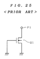
- FIG. 25 is a circuit diagram showing a connection example of an NMOS transistor for protection. As shown in FIG. 25, the drain of an NMOS transistor for protection Q 1 is connected to an I/O terminal P 1 , and the source and gate are grounded. An internal circuit (not shown) for performing the actual operation is also connected to the I/O terminal P 1 .
- the NMOS transistor for protection Q 1 When the normal voltage is applied to the I/O terminal P 1 , the NMOS transistor for protection Q 1 is in OFF state, causing no influence on the internal circuit. On the other hand, when an ESD occurs and the surge voltage SV is applied to the I/O terminal P 1 , the PN junction between an N type drain region and a P type well region (substrate) results in breakdown to discharge the surge voltage from the I/O terminal P 1 to a ground level (grounding terminal), thereby protecting the internal circuit.
- a field transistor has the structure in which an LOCOS oxide film is provided in place of the gate section (i.e., the gate oxide film and gate electrode) of an MOS transistor. Therefore, such a field transistor does not maintain the original transistor structure, but it is called field transistor in the technical fields that deal with ESD.
- the regions of a field transistor which correspond to the drain and source regions of an MOS transistor are also referred to as drain and source regions, respectively.
- An N type field transistor for protection (whose drain and source regions are of the N type) having the above-mentioned structure may be connected in the same manner as in the NMOS transistor for protection Q 1 shown in FIG. 25 . However, no potential setting is required for a LOCOS oxide film.
- an ESD protection element has been formed together with an internal circuit on a single semiconductor substrate under the same conditions.
- a semiconductor device having an ESD protection element comprises: a semiconductor substrate of a first conductivity type mainly composed of a first material; a first semiconductor region of a second conductivity type, formed in a surface of the semiconductor substrate; a second semiconductor region formed in a surface of the semiconductor substrate, independently of the first semiconductor region, edge portions in the first and second semiconductor regions opposed to each other being defined as first and second edge regions, respectively; and a semiconductor region for ESD protection of the first conductivity type, formed in a region of the semiconductor substrate including at least a region in the vicinity of a junction with the first and second edge portions, the semiconductor region for ESD protection being mainly composed of a second material having a smaller breakdown field than the first material.
- the semiconductor device having the ESD protection element of the first aspect further comprises: an insulting film on the semiconductor substrate between the first and second semiconductor regions; and a gate electrode on the insulating film.
- the semiconductor device having the ESD protection element of the first aspect further comprises an isolated insulating region, some of which projects from the semiconductor substrate between the first and second semiconductor regions, and the rest is buried in a surface of the semiconductor substrate.
- the semiconductor device having the ESD protection element of the first aspect is characterized in that the semiconductor region for ESD protection is selectively formed in an upper portion of the semiconductor substrate; and the first edge portion of the first semiconductor region and the second edge portion of the second semiconductor region are formed in the semiconductor region for ESD protection.
- the semiconductor device having the ESD protection element of the fourth aspect is characterized in that the semiconductor region for ESD protection includes first and second partial semiconductor regions for ESD spaced from each other in an upper portion of the semiconductor substrate; and the first edge portion is formed in the first partial semiconductor region for ESD, and the second edge portion is formed in the second partial semiconductor region for ESD.
- the semiconductor device having the ESD protection element of the fourth aspect further comprises a preliminary semiconductor region mainly composed of a specific material, interposed between the semiconductor substrate and the semiconductor region for ESD protection, the specific material containing a mixture of the first material and the second material.
- a method of manufacturing a semiconductor device having an ESD protection element comprises the steps of: (a) preparing a semiconductor substrate of a first conductivity type mainly composed of a first material; (b) selectively forming a semiconductor region for ESD protection mainly composed of a second material, in an upper portion of the semiconductor substrate, the second material having a smaller breakdown field than the first material; and (c) forming first and second semiconductor regions of a second conductivity type independently of each other in a surface of the semiconductor substrate including the semiconductor region for ESD protection, the step (c) forming first and second edge portions opposed to each other in the semiconductor region for ESD protection, the first and second edge portion being edge portions of the first and second semiconductor regions, respectively.
- the method of the seventh aspect is characterized in that: the step (b) includes performing an ion implantation of a specific material having a smaller breakdown field than the first material in an upper portion of the semiconductor substrate, to form the semiconductor region for ESD protection mainly composed of a mixture of the specific material and the first material; and the second material contains the mixture.
- the semiconductor region for ESD protection includes first and second partial semiconductor regions for ESD;
- the step (b) includes the steps of: (b-1) selectively forming a mask portion on the semiconductor substrate; and (b-2) performing an oblique ion implantation of the specific material from above the semiconductor substrate by using the mask portion as a mask, to form the first and second partial semiconductor regions for ESD spaced from each other so as to sandwich an underlying region of the mask region;
- the step (c) includes performing a vertical ion implantation of an impurity of a second conductivity type from above the semiconductor substrate by using the mask portion as a mask, to form the first and second semiconductor regions, the first edge portion being formed in the first partial semiconductor region for ESD, the second edge portion being formed in the second partial semiconductor region for ESD.
- step (b-1) includes the steps of: (b-1-1) selectively forming an insulating film on the semiconductor substrate; and (b-1-2) forming a gate electrode on the insulating film; and the mask portion includes the insulated film and the gate electrode.
- the second material contains a mixture of the first material and a specific material having a smaller breakdown field than the first material; and the step (b) includes the steps of: (b-1) forming a groove in an upper portion of the semiconductor substrate; and (b-2) forming the semiconductor region for ESD protection mainly composed of the second material in the groove by an epitaxial growth of the second material from the semiconductor substrate around the groove.
- the second material contains a material having a smaller breakdown field than the first material
- the step (b) includes the steps of: (b-1) forming a groove in an upper portion of the semiconductor substrate; (b-2) forming a preliminary semiconductor region mainly composed of a mixture of the first material and the second material along an inner periphery of the groove by an epitaxial growth of the mixture from the semiconductor substrate around the groove; and (b-3) forming a partial semiconductor region for ESD mainly composed of the second material in the groove including the preliminary semiconductor region by an epitaxial growth of the second material from the preliminary semiconductor region.
- the step (c) includes the steps of: (c-1) selectively forming an insulating film on the semiconductor substrate; (c-2) forming a gate electrode on the insulating film; and (c-3) forming the first and second semiconductor regions in a surface of the semiconductor substrate bed using portions including the gate electrode, as a mask.
- the method of the seventh aspect further comprises step (d), between the steps (a) and (b), of forming an isolated insulating film, some of which projects from the semiconductor substrate, and the rest is buried in a surface of the semiconductor substrate, wherein the step (c) includes forming the first and second semiconductor regions in a surface of the semiconductor substrate by using the isolated insulating film as a mask.
- a semiconductor region for ESD protection is formed in the region of a semiconductor substrate including at least the region in the vicinity of the junction with the first and second edge portions opposed to each other in first and second semiconductor regions.
- the semiconductor region for ESD protection is mainly composed of a second material having a smaller breakdown field than a first material which is the principal constituent of the semiconductor substrate.
- the PN junction of the ESD protection element causes a breakdown to discharge the serge voltage, at a voltage lower than that in the case where the semiconductor region for ESD protection is mainly composed of the first material.
- An element for use in the normal operation can be formed without degrading its operation characteristics, by forming it in the semiconductor substrate mainly composed of the first material.
- the semiconductor device having the ESD protection element of the second aspect has an insulating film formed on the semiconductor substrate between the first and second semiconductor regions, and a gate electrode formed on the insulating film.
- the semiconductor device having the ESD protection element of the third aspect has an isolated insulating region, some of which projects from the semiconductor substrate between the first and second semiconductor region, and the rest is buried in the surface of the semiconductor substrate.
- a semiconductor region for ESD protection is selectively formed in the upper portion of a semiconductor substrate. Therefore, it is relatively easy to form an ESD protection element mainly composed of a second material which comprises a mixture of a first material and a specific material, by performing, for example, an ion implantation of the specific material having a smaller breakdown field than the first material, from above the semiconductor substrate.
- the semiconductor region for ESD protection includes a first partial semiconductor region for ESD wherein a first edge portion is present, and a second partial semiconductor region for ESD wherein a second edge portion is present. This enables to obtain an ESD protection element excellent in ESD resistance while minimizing the region for forming the semiconductor region for ESD protection.
- the semiconductor device having the ESD protection element of the sixth aspect has a preliminary semiconductor region that is interposed between a semiconductor substrate and the semiconductor region for ESD protection, and is mainly composed of a specific material containing a mixture of first and second materials.
- a semiconductor region for ESD protection mainly composed of the second material by performing, for example, an epitaxial growth of a specific material (a mixture of the first and second materials) from above the semiconductor substrate, to form a preliminary semiconductor region mainly composed of the specific material, and then performing an epitaxial growth of the second material from the preliminary semiconductor region.
- a specific material a mixture of the first and second materials
- the semiconductor region for ESD protection mainly composed of the second material completely different from the first material.
- step (b) a semiconductor region for ESD protection mainly composed of a second material having a smaller breakdown voltage than a first material is selectively formed on the upper portion of a semiconductor substrate, and in step (c) the first and second semiconductor regions of a second conductivity type are formed in the surface of the semiconductor substrate including the semiconductor region for ESD protection.
- step (c) first and second edge portions which are the edge portions of the first and second semiconductor regions and face with each other, are formed in the semiconductor region for ESD protection.
- the PN junction of the ESD protection element causes a breakdown to discharge the serge voltage, at a voltage lower than that in the case where the semiconductor region for ESD protection is mainly composed of the first material.
- an element for use in the normal operation can be formed without degrading its operation characteristics, by forming it in the semiconductor substrate mainly composed of the first material in other manufacturing step.
- step (b) includes performing an ion implantation of a specific material having a smaller breakdown field than a first material in the upper portion of a semiconductor substrate, to form a semiconductor region for ESD protection mainly composed of a mixture of the first material and a specific material.
- a semiconductor region for ESD protection mainly composed of a second material, which is a mixture of the specific material and the first material, can be obtained with a relatively simple ion implantation processing.
- step (b-2) in the method of manufacturing an ESD protection element according to the ninth aspect, in step (b-2), hb using a mask portion selectively formed on the semiconductor substrate as a mask, an oblique rotational ion implantation of a specific material is performed from above a semiconductor substrate, to form first and second partial semiconductor regions for ESD which are isolated by the underlying region of the mask portion.
- step (b-1) comprises step (b-1-1) of selectively forming an insulating film on a semiconductor substrate, and step (b-1-2) of forming a gate electrode on the insulating film, so that a mask portion includes the insulating film and the gate electrode.
- an ESD protection element having the MOS transistor structure by connecting, for example, a first semiconductor region to an I/O terminal and setting the potential between the gate electrode and a second semiconductor region so as not to enter ON state in the normal state.
- the first and second partial semiconductor regions for ESD can be formed in the self alignment manner in the oblique rotational ion implantation of the specific material.
- step (b-2) a second material that is a mixture of a first material and a specific material having a smaller breakdown field than the first material, is epitaxially grown from the semiconductor substrate around a groove so that a semiconductor region for ESD protection mainly composed of the second material is formed in the groove. Therefore, a semiconductor region for ESD protection mainly composed of the second material which is a mixture of the specific material and the first material can be obtained by employing epitaxial growth method.
- step (b-2) a mixture of first and second materials is epitaxially grown from the semiconductor substrate to form a preliminary semiconductor region mainly composed of the mixture, and in step (b-3) the second material is epitaxially grown from the preliminary semiconductor region to form a partial semiconductor region for ESD mainly composed of the second material.
- step (b-3) the second material is epitaxially grown from the preliminary semiconductor region to form a partial semiconductor region for ESD mainly composed of the second material.
- step (c) includes step (c-1) of selectively forming an insulating film on a semiconductor substrate, step (c-2) of forming a gate electrode on the insulating film, and step (c-3) of forming first and second semiconductor regions on the surface of the semiconductor substrate by using the gate electrode as a mask. Therefore, it is possible to obtain an ESD protection element having the MOS transistor structure by connecting, for example, the first semiconductor region to an I/O terminal and setting the potential between the gate electrode and the second semiconductor region so as not to enter ON state in the normal state.
- the method of manufacturing a semiconductor device having an ESD protection element according to the fourteenth aspect includes step (d), between steps (a) and (b), of forming an isolated insulating film, some of which projects from a semiconductor substrate, and the rest is buried in the semiconductor substrate. This permits an ESD protection element having the field transistor structure which always enters OFF state in the normal state by connecting, for example, the first semiconductor region to an I/O terminal.
- an object of the present invention is to obtain a semiconductor device having an ESD protection element with an improved ESD resistance even when it is formed on a single substrate together with an internal circuit.
- FIG. 1 is a cross-sectional view of the structure of an MOS transistor for protection according to a first preferred embodiment of the present invention
- FIG. 2 is a graph showing the current changes with time when an MOS transistor for protection makes a discharge operation
- FIG. 3 is a graph showing the current and voltage changes when an MOS transistor for protection and an MOS transistor for internal circuit make a discharge operation, respectively;
- FIG. 4 is a graph showing the temperature changes with time when an MOS transistor for protection and an MOS transistor for internal circuit make a discharge operation, respectively;
- FIG. 5 is a cross-sectional view illustrating a manufacturing step in a method of manufacturing an MOS transistor for protection according to the first preferred embodiment
- FIG. 6 is a cross-sectional view illustrating another manufacturing step in the method of the first preferred embodiment
- FIG. 7 is a cross-sectional view illustrating another manufacturing step in the method of the first preferred embodiment
- FIG. 8 is a cross-sectional view illustrating another manufacturing step in the method of the first preferred embodiment
- FIG. 9 is a cross-sectional view illustrating a manufacturing step in a method of manufacturing an MOS transistor for protection according to a second preferred embodiment of the present invention.
- FIG. 10 is a cross-sectional view illustrating another manufacturing step in the method of the second preferred embodiment
- FIG. 11 is a cross-sectional view illustrating another manufacturing step in the method of the second preferred embodiment
- FIG. 12 is a cross-sectional view illustrating another manufacturing step in the method of the second preferred embodiment
- FIG. 13 is a cross-sectional view illustrating another manufacturing step in the method of the second preferred embodiment
- FIG. 14 is a cross-sectional view illustrating an example of a modified MOS transistor for protection of the second preferred embodiment
- FIG. 15 is a cross-sectional view of the structure illustrating a field transistor for protection according to a third preferred embodiment of the present invention.
- FIG. 16 is a cross-sectional view illustrating a manufacturing step in a method of manufacturing a field transistor for protection according to the third preferred embodiment
- FIG. 17 is a cross-sectional view illustrating another manufacturing step in the method of the third preferred embodiment.
- FIG. 18 is a cross-sectional view illustrating another manufacturing step in the method of the third preferred embodiment.
- FIG. 19 is a cross-sectional view illustrating another manufacturing step in the method of the third preferred embodiment.
- FIG. 20 is a cross-sectional view of the structure of an MOS transistor for protection according to a fourth preferred embodiment of the present invention.
- FIG. 21 is a cross-sectional view illustrating a manufacturing step in a method of manufacturing an MOS transistor for protection according to the fourth preferred embodiment
- FIG. 22 is a cross-sectional view illustrating another manufacturing step in the method of the fourth preferred embodiment.
- FIG. 23 is a cross-sectional view illustrating another manufacturing step in the method of the fourth preferred embodiment.
- FIG. 24 is a cross-sectional view illustrating another manufacturing step in the method of the fourth preferred embodiment.
- FIG. 25 is a circuit diagram showing a configuration of a conventional MOS transistor for protection.
- Silicon (Si) substrates made of silicon are often employed as a semiconductor substrate. Meanwhile, the breakdown field of germanium (Ge) is 80 kV/cm, which is lower than that of Si, i.e., 300 kV/cm. Therefore, the formation of an ESD protection element in the region of Ge or silicon germanium (SiGe) may improve ESD resistance because its breakdown field is reduced compared to the formation in the region mainly composed of Si.
- ESD resistance a further improvement of ESD resistance than prior art can be expected by forming an ESD protection element in which opposed edge portions in the drain and source regions form a PN junction with the region of Ge or SiGe. This is because the field concentration occurs at these edge portions when a surge voltage is applied.
- the region mainly composed of Ge or SiGe can be formed on an Si substrate by an ion implantation of Ge to the Si substrate, or by an epitaxial growth of SiGe (and Ge).
- FIG. 1 is a cross-sectional view showing the structure of an MOS transistor for protection according to a first preferred embodiment of the present invention.
- a P well region 10 is selectively formed in the upper portion of a P type Si substrate 1 (in FIG. 1, the region 10 is formed in the enter surface, but in practice it is formed only on part of the upper portion of the Si substrate 1 ).
- the P well region 10 comprises an Si—P well region 2 mainly composed of Si, and an SiGe—P well region 3 mainly composed of SiGe.
- the SiGe—P well region 3 is formed on the Si—P well region 2 .
- a drain region 4 and a source region 5 are selectively formed in the surface of the SiGe—P well region 3 .
- a gate oxide film 6 is formed on the SiGe—P well region 3 extending between the drain region 4 and the source region 5 .
- a gate polysilicon layer 7 serving as a gate electrode is formed on the gate oxide film 6 .
- An oxide film 8 is formed on the gate polysilicon layer 7 . Sidewalls 9 are formed on the portions of the drain region 4 and the source region 5 adjacent to the gate oxide film 6 , the gate polysilicon layer 7 , and the oxide film 8 .
- MOS transistor for protection comprising the SiGe—P well region 3 , the, drain region 4 , the source region 5 , the gate oxide film 6 , and the gate polysilicon layer 7 .
- An MOS transistor for internal circuit (not shown) is also formed directly on the Si substrate 1 , or formed in a well region mainly composed of Si. Therefore, the operation characteristics of the MOS transistor for internal circuit may not deteriorate.
- the MOS transistor for protection having the above structure is formed on the SiGe region, the breakdown voltage of the junction between the source and drain is lower than that of the MOS transistor for internal circuit which is formed on a P type Si region.
- FIG. 2 is a graph showing the result of simulation of the discharge operation in an MOS transistor for protection when an ESD occurs.
- the drain current Id is plotted as ordinate and the time elapsed as abscissa. As can be seen from this graph, initially the drain current Id flows in large quantities, and thereafter, the quantity of the drain current Id is reduced with time.
- FIG. 3 is a graph showing the results of simulations of both discharge operations in an MOS transistor for protection and an MOS transistor for internal circuit when an ESD occurs.
- the drain current Id is plotted as ordinate and the drain voltage Vd as abscissa
- L 1 indicates the result of the MOS transistor for protection
- L 2 indicates the result of the MOS transistor for interrial circuit.
- Ideogram ⁇ circle around (1) ⁇ denotes the behavior until the MOS transistor for protection and the MOS transistor for internal circuit reach the breakdown voltage VBD 1 and VBD 2 , respectively;
- ideogram ⁇ circle around (2) ⁇ denotes the behavior until a peak current flows after the breakdown;
- ideogram ⁇ circle around (3) ⁇ denotes the behavior after the peak current flows.
- the breakdown voltage VBD 1 of the MOS transistor for protection is lower than the breakdown voltage VBD 2 of the MOS transistor for internal circuit.
- FIG. 4 is a graph showing the temperature changes with time during the operations of the MOS transistor for protection and the MOS transistor for internal circuit shown in FIG. 3 .
- the temperature is plotted as ordinate and the time elapsed as abscissa, and L 11 (broken line) indicates the result of the MOS transistor for protection, and L 12 (solid line) indicates the result of the MOS transistor for internal circuit.
- the breakdown voltage VBD 1 of the MOS transistor for protection is lower than the breakdown voltage VBD 2 of the MOS transistor for internal circuit, and therefore, the rise of the temperature is retarded in the former. That is, compared to the MOS transistor for internal circuit, the MOS transistor for protection is resistant to thermal breakdown and suppresses the temperature rise more satisfactorily, thus permitting the improvement of ESD resistance.
- the drain region 4 and the source region 5 of the MOS transistor for protection is formed in the SiGe—P well region 3 (i.e., a semiconductor region for ESD protection) formed in the upper portion of the Si substrate 1 . It is therefore possible to obtain a favorable ESD resistance without degrading the performance of the MOS transistor for internal circuit.
- FIGS. 5 to 8 are a cross-sectional view illustrating a manufacturing step in a method of manufacturing the MOS transistor for protection shown in FIG. 1, according to the first preferred embodiment. Its manufacturing steps will be described hereafter by referring to these figures.
- an ion implantation of Ge is conducted to an Si substrate 1 at an energy of 100 KeV and a dosage of 1 ⁇ 10 14 cm ⁇ 2 , to from an SiGe latter 11 mainly composed of SiGe in the upper portion of the Si substrate 1 .
- the energy is set so that the SiGe layer 11 is thicker than the source and drain regions of the ultimately formed MOS transistor.
- the dosage is set so that the MOS transistor to be formed on the SiGe layer 11 has a breakdown voltage lower than that of the MOS transistor to be formed on the Si substrate 1 or a well region of Si.
- an ion implantation of boron (B) (i.e., a first ion implantation) is conducted at an energy of 120 KeV and a dosage of 1 ⁇ 10 12 cm ⁇ 2
- another ion implantation of boron (B) (i.e., a second ion implantation) is conducted at an energy of 70 KeV and a dosage of 1 ⁇ 10 13 cm ⁇ 2 , to form a P well region 10 .
- the region mainly composed of Si becomes an Si—P well region 2 and the region mainly composed of SiGe becomes an SiGe—P well region 3 .
- the main object of the first ion implantation is to increase the P type impurity concentration of the under portion of the P well region 10 , in order to prevent the punch through phenomenon of the MOS transistor.
- the object of the second ion implantation is to increase the P type impurity concentration of the upper portion of the P well region 10 , in order to adjust the threshold voltage.
- a gate oxide film 6 is selectively formed on the SiGe—P well region 3 , and a gate polysilicon layer 7 serving as a gate electrode is formed on the gate oxide film 6 .
- a gate polysilicon layer 7 serving as a gate electrode is formed on the gate oxide film 6 .
- an oxide film 8 By using the oxide film 8 (the gate oxide film 6 , the gate polysilicon film 7 ) as a mask, an ion implantation of phosphorus (P) is conducted at an energy of 30 KeV and a dosage of 2 ⁇ 10 13 cm ⁇ 2 , to form a drain region 4 A and a source region 5 A in the surface of the SiGe—P well region 3 .
- sidewalls 9 composed of an oxide film are formed on the sides of the gate oxide film 6 , the gate polysilicon layer 7 , and the oxide film 8 . Then, by using the oxide film 8 and the sidewalls 9 as a mask, an ion implantation of arsenic (As) is conducted at an energy of 30 KeV and a dosage of 1 ⁇ 10 15 cm ⁇ 2 , and a heat treatment is performed at 820° C. for 15 minutes, so that a drain region 4 and a source region 5 are formed by double diffusion, resulting in the MOS transistor for protection having the structure shown in FIG. 1 .
- Ars arsenic
- the MOS transistor for protection excellent in ESD resistance can be formed on the Si substrate 1 by means of ion implantation.
- FIG. 9 is a cross-sectional view showing the structure of an MOS transistor for protection according to a second preferred embodiment of the present invention.
- a P well region 20 is selectively formed in the upper portion of a P type Si substrate 1 (in FIG. 9, the region 20 is formed in the enter surface, but in practice it is formed only in part of the upper portion of the Si substrate 1 ).
- the P well region 20 comprises an Si—P well region 12 mainly composed of Si, and an SiGe—P well region 13 mainly composed of SiGe.
- the SiGe—P well region 13 is buried in the upper portion of the Si—P well region 12 .
- a drain region 4 and a source region 5 are selectively formed in the surfaces of the Si—P well region 12 and the SiGe—P well region 13 .
- edge portions 4 E and 5 E in the drain region 4 and the source region 5 opposed to each other, respectively, are formed in the SiGe—P well region 13 .
- a gate oxide film 6 is formed on the SiGe—P well region 13 extending between the drain region 4 and the source region 5 .
- a gate polysilicon layer 7 serving as a gate electrode is formed on the gate oxide film 6 .
- An oxide film 8 is formed on the gate polysilicon latter 7 .
- Sidewalls 9 are formed on the portions of the drain region 4 and the source region 5 adjacent to the gate oxide film 6 , the gate polysilicon layer 7 , and the oxide film 8 .
- MOS transistor for protection comprising the SiGe—P well region 13 , the drain region 4 , the source region 5 , the gate oxide film 6 , and the gate polysilicon layer 7 .
- An MOS transistor for internal circuit (not shown) is also formed in a region mainly composed of Si, such as the Si substrate 1 .
- the edge portions 4 E, 5 E in the drain and source regions 4 and 5 opposed to each other, respectively, are present in the SiGe—P well region 13 (a semiconductor region for ESD protection). Therefore, like the first preferred embodiment, a favorable ESD resistance can be obtained without degrading the performance of the MOS transistor for internal circuit.
- FIGS. 10 to 13 are a cross-sectional view illustrating a manufacturing step in a method of manufacturing the MOS transistor for protection shown in FIG. 9, according to the second preferred embodiment. Its manufacturing steps will be described hereafter by referring to these figures.
- the upper portion of an Si substrate 1 is selectively etched to form a groove, and SiGe is epitaxially grown from the Si substrate 1 extending around the groove, so that an SiGe layer 21 mainly composed of SiGe is formed in the groove.
- an epitaxial growth method there are an MBE (molecular beam epitaxy) method and a CVD (chemical vapor deposition), and the like.
- an ion implantation of boron is conducted two times to form a P well region 20 .
- the region mainly composed of Si i.e., the Si substrate 1
- the region mainly composed of SiGe i.e., an SiGe layer 21
- FIGS. 12 and 13 the same manufacturing steps as shown in FIGS. 7 and 8 are carried out to obtain an MOS transistor for protection of the second preferred embodiment.
- FIG. 14 is a cross-sectional view of a modified MOS transistor for protection of the second preferred embodiment.
- a P well region 16 is formed in the upper portion of an Si substrate 1 .
- the P well region 16 comprises an Si—P well region 12 mainly composed of Si, an SiGe region 14 mainly composed of SiGe, and a Ge—P well region 15 mainly composed of Ge.
- the Ge—P well region 15 is buried in the upper portion of the Si—P well region 12 through the SiGe region 14 .
- a drain region 4 and a source region 5 are selectively formed in the surfaces of the Si—P well region 12 , the SiGe region 14 , and the Ge—P well region 15 .
- edge portions 4 E and 5 E in the drain and source regions 4 and 5 opposed to each other, respectively, are formed in the Ge—P well region 15 .
- Other structural features of this modified transistor are the same as those shown in FIG. 9 .
- the opposed edge portions 4 E and 5 E of the drain and source regions 4 and 5 are present in the Ge—P well region 15 mainly composed of Ge. This permits a higher ESD resistance than that of the structure shown in FIG. 9, because the principal constituent of that region is Ge instead of SiGe.
- SiGe is epitaxially grown from the Si substrate 1 extending around the groove, so that an SiGe region mainly composed of SiGe is formed along the inner periphery of the groove.
- Ge is epitaxially grown from the SiGe region, so that a Ge-Well region is formed in the groove including the SiGe region.
- the region mainly composed of Si i.e., the Si substrate 1
- the region mainly composed of SiGe becomes an SiGe region 14
- the region mainly composed of Ge becomes a Ge—P well region 15 .
- FIG. 15 is a cross-sectional view showing the structure of a field transistor for protection according to a third preferred embodiment of the present invention.
- a P well region 30 is selectively formed in the upper portion of a P type Si substrate 1 (in FIG. 15, the region 30 is formed in the enter surface, but in practice it is formed only on part of the upper portion of the Si substrate 1 ).
- the P well region 30 comprises an Si—P well region 22 mainly composed of Si, and an SiGe—P well region 23 mainly composed of SiGe.
- the SiGe—P well region 23 is formed on the Si—P well region 22 .
- LOCOS oxide film 26 There is formed an LOCOS oxide film 26 , some of which is buried in the surface of the SiGe—P well region 23 , and the rest projects from the surface of the SiGe—P well region 23 .
- a drain region 24 and a source region 25 are formed so as to sandwich the LOCOS oxide film 26 in the surface of the SiGe—P well region 23 .
- a field transistor for protection which comprises the SiGe—P well region 23 , the drain region 24 , the source region 25 , and the LOCOS oxide film 26 . Also, a field transistor for internal circuit (not shown) is formed directly on the Si substrate 1 .
- the drain region 4 and the source region 5 are formed in the SiGe—P well region 23 (a semiconductor region for ESD protection). Therefore, a favorable ESD resistance can be obtained without degrading the performance of the field transistor for internal circuit.
- FIGS. 16 to 19 are a cross-sectional view illustrating a manufacturing step in a method of manufacturing the field transistor for protection shown in FIG. 15, according to the third preferred embodiment. Its manufacturing steps will be described hereafter by referring to these figures.
- an LOCOS film 26 having a thickness of 4000 ⁇ is formed, some of which is buried in the surface of an Si substrate 1 , and the rest projects from the surface of the Si substrate 1 .
- an ion implantation of Ge is conducted to the Si substrate 1 at an energy of 100 KeV and a dosage of 1 ⁇ 10 14 cm ⁇ 2 , so that an SiGe layer 31 mainly composed of SiGe is formed in the upper portion of the Si substrate 1 .
- the energy is set so that the SiGe layer 31 is thicker than the source and drain regions of the ultimately formed field transistor.
- the dosage is set so that the breakdown voltage of the field transistor to be formed on the SiGe layer 31 is satisfactorily lower than that of the transistor to be directly formed on the Si substrate 1 .
- an ion implantation of boron (B) is conducted at an energy of 120 KeV and a dosage of 1 ⁇ 10 12 cm ⁇ 2
- another ion implantation of boron is conducted at an energy of 70 KeV and a dosage of 1 ⁇ 10 13 cm ⁇ 2 , to form a P well region 30 .
- the region mainly composed of Si L becomes an Si—P well region 22
- the region mainly composed of SiGe becomes an SiGe—P well region 23 .
- the object of the former ion implantation is to prevent the punch through phenomenon of the field transistor, and that of the latter is to adjust the threshold voltage, as in the first preferred embodiment.
- an ion implantation of phosphorus (P) is conducted at an energy of 30 KeV and a dosage of 2 ⁇ 10 13 cm ⁇ 2 , so that a drain region 24 A and a source region 25 A are formed in the surface of the SiGe—P well region 23 . Since an LOCOS oxide film 26 is thick, the phosphorus (P) may not reach the SiGe—P well region 23 underlying the LOCOS oxide film 26 .
- an ion implantation of arsenic (As) is conducted at an energy of 30 KeV and a dosage of 1 ⁇ 10 15 cm ⁇ 2 , and a heat treatment is performed at 820° C. for 15 minutes, so that a drain region 24 and a source region 25 are formed by double diffusion, resulting in the field transistor for protection shown in FIG. 15 .
- As arsenic
- the field transistor for protection excellent in ESD resistance can be formed on the Si substrate 1 by means of ion implantation.
- FIG. 20 is a cross-sectional view showing the structure of an MOS transistor for protection according to a fourth preferred embodiment of the present invention.
- a P well region 40 is selectively formed in the upper portion of a P type Si substrate 1 (in FIG. 20, the region 40 is formed in the enter surface, but in practice it is formed only on part of the upper portion of the Si substrate 1 ).
- SiGe—P well regions 41 A, 41 B are formed apart in the upper portions of the P well region 40 .
- a drain region 4 is selectively formed in the surface of the SiGe—P well region 41 A, and a source region 5 is selectively formed in the surface of the SiGe—P well region 41 B.
- a gate oxide film 6 is formed in the P well region 40 (including the SiGe—P well regions 41 A, 41 B) extending between the drain region 4 and the source region 5 .
- a gate polysilicon layer 7 serving as a gate electrode is formed on the gate oxide film 6 .
- An oxide film 8 is formed on the gate polysilicon layer 7 .
- Sidewalls 9 are formed on the portions of the drain region 4 and the source region 5 adjacent to the gate oxide film 6 , the gate polysilicon layer 7 , and the oxide film 8 .
- MOS transistor for protection which comprises the P well region 40 (including the SiGe—P well regions 41 A, 41 B), the drain region 4 , the source region 5 , the gate oxide film 6 , and the gate polysilicon layer 7 . Also, an MOS transistor for internal circuit (not shown) is formed directly on the Si substrate 1 .
- the drain region 4 and the source region 5 are formed in the SiGe—P well regions 41 A and 41 B mainly composed of SiGe (a semiconductor region for ESD protection), respectively. Therefore, the breakdown voltage of the junction between the source and drain is lower than that of the MOS transistor for internal circuit which is formed in a region mainly composed of a P type Si.
- the MOS transistor for protection of the fourth preferred embodiment permits a favorable ESD resistance without degrading the performance of the MOS transistor for internal circuit.
- the region mainly composed of SiGe is minimized because the edge portion 4 E of the drain region 4 and the edge portion 5 E of the source region 5 are present in the SiGe—P well region 41 A and the SiGe—P well region 41 B, respectively.
- FIGS. 21 to 24 are a cross-sectional view illustrating a manufacturing step in a method of manufacturing the MOS transistor for protection shown in FIG. 20, according to the fourth preferred embodiment. Its manufacturing steps will be described hereafter by referring to these figures.
- an ion implantation of boron (B) (i.e., a first ion implantation) is conducted at an energy of 120 KeV and a dosage of 1 ⁇ 10 12 cm ⁇ 2
- another ion implantation of boron (B) i.e., a second ion implantation
- the main object of the first ion implantation is to increase the P type impurity concentration of the under portion of the P well region 40 , in order to prevent the punch through phenomenon of the MOS transistor.
- the object of the second ion implantation is to increase the P type impurity concentration of the upper portion of the P well region 40 , in order to adjust the threshold voltage.
- a gate oxide film 6 is selectively formed on the P well region 40 , and a gate polysilicon layer 7 serving as a gate electrode is formed on the gate oxide film 6 .
- a gate polysilicon layer 7 serving as a gate electrode is formed on the gate oxide film 6 .
- An oblique rotational ion implantation of Ge is conducted from above to the P well region 40 at an energy of 100 KeV and a dosage of 1 ⁇ 10 14 cm ⁇ 2 , so that SiGe—P well regions 41 A, 41 B are formed in the upper portions of the P well region 40 . This results in the SiGe—P well regions 41 A and 41 B, part of which underlies the gate oxide film 6 .
- the energy is set so that the SiGe—P well regions 41 A, 41 B are thicker than the source and drain regions of the ultimately formed MOS transistor.
- the dosage is set so that the breakdown voltage of the MOS transistor whose drain and source will be formed in the SiGe—P well regions 41 A and 41 B, respectively, is satisfactorily lower than that of the MOS transistor whose drain and source will be directly formed on the Si substrate 1 .
- a vertical ion implantation of phosphorus (P) is conducted from above at an energy of 30 KeV and a dosage of 2 ⁇ 10 13 cm ⁇ 2 , so that a drain region 4 A and a source region 5 A are formed in the surfaces of the SiGe—P well regions 41 A and 41 B, respectively.
- sidewalls 9 comprising an oxide film are formed on the sides of the gate oxide film 6 , the gate polysilicon layer 7 , and the oxide film 8 . Then, by using the oxide film 8 and the sidewalls 9 as a mask, a vertical ion implantation of arsenic (As) is conducted from above at an energy of 30 KeV and a dosage of 1 ⁇ 10 15 cm ⁇ 2 , and a heat treatment is performed at 820° C. for 15 minutes, so that a drain region 4 and a source region 5 are formed by double diffusion, resulting in the MOS transistor for protection having the structure shown in FIG. 20 .
- Arsenic arsenic
- the MOS transistor for protection excellent in ESD resistance can be formed on the Si substrate 1 by means of ion implantation.
- the present invention is, of course, applicable to any kind of ESD protection elements with the above mentioned structure, having a semiconductor region for ESD protection which is formed by a second material having a smaller breakdown field than a first material that is the principal constituent of the substrate.
Abstract
Description
Claims (10)
Priority Applications (1)
| Application Number | Priority Date | Filing Date | Title |
|---|---|---|---|
| US09/667,497 US6696341B1 (en) | 1998-01-21 | 2000-09-22 | Method of manufacturing a semiconductor device having electrostatic discharge protection element |
Applications Claiming Priority (4)
| Application Number | Priority Date | Filing Date | Title |
|---|---|---|---|
| JP10009592A JPH11214627A (en) | 1998-01-21 | 1998-01-21 | Esd protection element and manufacture thereof |
| JPP10-009592 | 1998-01-21 | ||
| US09/092,019 US6198135B1 (en) | 1998-01-21 | 1998-06-05 | Semiconductor device having electrostatic discharge protection element and manufacturing method thereof |
| US09/667,497 US6696341B1 (en) | 1998-01-21 | 2000-09-22 | Method of manufacturing a semiconductor device having electrostatic discharge protection element |
Related Parent Applications (1)
| Application Number | Title | Priority Date | Filing Date |
|---|---|---|---|
| US09/092,019 Division US6198135B1 (en) | 1998-01-21 | 1998-06-05 | Semiconductor device having electrostatic discharge protection element and manufacturing method thereof |
Publications (1)
| Publication Number | Publication Date |
|---|---|
| US6696341B1 true US6696341B1 (en) | 2004-02-24 |
Family
ID=31497325
Family Applications (1)
| Application Number | Title | Priority Date | Filing Date |
|---|---|---|---|
| US09/667,497 Expired - Fee Related US6696341B1 (en) | 1998-01-21 | 2000-09-22 | Method of manufacturing a semiconductor device having electrostatic discharge protection element |
Country Status (1)
| Country | Link |
|---|---|
| US (1) | US6696341B1 (en) |
Cited By (8)
| Publication number | Priority date | Publication date | Assignee | Title |
|---|---|---|---|---|
| US20040072394A1 (en) * | 2002-10-10 | 2004-04-15 | Matsushita Electric Industrial Co., Ltd. | Semiconductor device and method for fabricating the same |
| US20040121524A1 (en) * | 2002-12-20 | 2004-06-24 | Micron Technology, Inc. | Apparatus and method for controlling diffusion |
| US20040212046A1 (en) * | 2003-04-22 | 2004-10-28 | Micron Technology, Inc. | Controlling diffusion in doped semiconductor regions |
| US20060073643A1 (en) * | 2004-02-03 | 2006-04-06 | Hong-Jyh Li | Transistor with doped gate dielectric |
| US20060228875A1 (en) * | 2004-03-22 | 2006-10-12 | Hong-Jyh Li | Transistor with shallow germanium implantation region in channel |
| US20070048953A1 (en) * | 2005-08-30 | 2007-03-01 | Micron Technology, Inc. | Graded dielectric layers |
| US20070123010A1 (en) * | 2005-11-30 | 2007-05-31 | Jan Hoentschel | Technique for reducing crystal defects in strained transistors by tilted preamorphization |
| US10411120B2 (en) * | 2016-08-12 | 2019-09-10 | International Business Machines Corporation | Self-aligned inner-spacer replacement process using implantation |
Citations (22)
| Publication number | Priority date | Publication date | Assignee | Title |
|---|---|---|---|---|
| US4509067A (en) | 1981-06-23 | 1985-04-02 | Tokyo Shibaura Denki Kabushiki Kaisha | Semiconductor integrated circuit devices with protective means against overvoltages |
| USRE33693E (en) | 1985-06-05 | 1991-09-17 | At&T Bell Laboratories | Device using ordered semiconductor alloy |
| JPH0434942A (en) | 1990-05-30 | 1992-02-05 | Nec Corp | Manufacture of semiconductor device |
| US5095358A (en) * | 1990-04-18 | 1992-03-10 | National Semiconductor Corporation | Application of electronic properties of germanium to inhibit n-type or p-type diffusion in silicon |
| US5245208A (en) * | 1991-04-22 | 1993-09-14 | Mitsubishi Denki Kabushiki Kaisha | Semiconductor device and manufacturing method thereof |
| US5312766A (en) | 1991-03-06 | 1994-05-17 | National Semiconductor Corporation | Method of providing lower contact resistance in MOS transistors |
| US5360749A (en) * | 1993-12-10 | 1994-11-01 | Advanced Micro Devices, Inc. | Method of making semiconductor structure with germanium implant for reducing short channel effects and subthreshold current near the substrate surface |
| US5698869A (en) | 1994-09-13 | 1997-12-16 | Kabushiki Kaisha Toshiba | Insulated-gate transistor having narrow-bandgap-source |
| US5885886A (en) * | 1996-12-26 | 1999-03-23 | Lg Semicon Co., Ltd. | Method for manufacturing semiconductor device |
| US5891792A (en) | 1998-08-14 | 1999-04-06 | Taiwan Semiconductor Manufacturing Company, Ltd. | ESD device protection structure and process with high tilt angle GE implant |
| US6087209A (en) * | 1998-07-31 | 2000-07-11 | Advanced Micro Devices, Inc. | Formation of low resistance, ultra shallow LDD junctions employing a sub-surface, non-amorphous implant |
| US6130144A (en) * | 1997-01-02 | 2000-10-10 | Texas Instruments Incorporated | Method for making very shallow junctions in silicon devices |
| US6180476B1 (en) * | 1998-11-06 | 2001-01-30 | Advanced Micro Devices, Inc. | Dual amorphization implant process for ultra-shallow drain and source extensions |
| US6184112B1 (en) * | 1998-12-02 | 2001-02-06 | Advanced Micro Devices, Inc. | Method of forming a MOSFET transistor with a shallow abrupt retrograde dopant profile |
| US6198135B1 (en) * | 1998-01-21 | 2001-03-06 | Mitsubishi Denki Kabushiki Kaisha | Semiconductor device having electrostatic discharge protection element and manufacturing method thereof |
| USRE37158E1 (en) * | 1990-08-09 | 2001-05-01 | Micron Technology, Inc. | High performance sub-micron P-channel transistor with germanium implant |
| US6297115B1 (en) * | 1998-11-06 | 2001-10-02 | Advanced Micro Devices, Inc. | Cmos processs with low thermal budget |
| US6380590B1 (en) * | 2001-02-22 | 2002-04-30 | Advanced Micro Devices, Inc. | SOI chip having multiple threshold voltage MOSFETs by using multiple channel materials and method of fabricating same |
| US6395587B1 (en) * | 2000-02-11 | 2002-05-28 | International Business Machines Corporation | Fully amorphized source/drain for leaky junctions |
| US6445016B1 (en) * | 2001-02-28 | 2002-09-03 | Advanced Micro Devices, Inc. | Silicon-on-insulator (SOI) transistor having partial hetero source/drain junctions fabricated with high energy germanium implantation |
| US6475885B1 (en) * | 2001-06-29 | 2002-11-05 | Advanced Micro Devices, Inc. | Source/drain formation with sub-amorphizing implantation |
| US6486510B2 (en) * | 2000-03-30 | 2002-11-26 | International Business Machines Corporation | Reduction of reverse short channel effects by implantation of neutral dopants |
-
2000
- 2000-09-22 US US09/667,497 patent/US6696341B1/en not_active Expired - Fee Related
Patent Citations (22)
| Publication number | Priority date | Publication date | Assignee | Title |
|---|---|---|---|---|
| US4509067A (en) | 1981-06-23 | 1985-04-02 | Tokyo Shibaura Denki Kabushiki Kaisha | Semiconductor integrated circuit devices with protective means against overvoltages |
| USRE33693E (en) | 1985-06-05 | 1991-09-17 | At&T Bell Laboratories | Device using ordered semiconductor alloy |
| US5095358A (en) * | 1990-04-18 | 1992-03-10 | National Semiconductor Corporation | Application of electronic properties of germanium to inhibit n-type or p-type diffusion in silicon |
| JPH0434942A (en) | 1990-05-30 | 1992-02-05 | Nec Corp | Manufacture of semiconductor device |
| USRE37158E1 (en) * | 1990-08-09 | 2001-05-01 | Micron Technology, Inc. | High performance sub-micron P-channel transistor with germanium implant |
| US5312766A (en) | 1991-03-06 | 1994-05-17 | National Semiconductor Corporation | Method of providing lower contact resistance in MOS transistors |
| US5245208A (en) * | 1991-04-22 | 1993-09-14 | Mitsubishi Denki Kabushiki Kaisha | Semiconductor device and manufacturing method thereof |
| US5360749A (en) * | 1993-12-10 | 1994-11-01 | Advanced Micro Devices, Inc. | Method of making semiconductor structure with germanium implant for reducing short channel effects and subthreshold current near the substrate surface |
| US5698869A (en) | 1994-09-13 | 1997-12-16 | Kabushiki Kaisha Toshiba | Insulated-gate transistor having narrow-bandgap-source |
| US5885886A (en) * | 1996-12-26 | 1999-03-23 | Lg Semicon Co., Ltd. | Method for manufacturing semiconductor device |
| US6130144A (en) * | 1997-01-02 | 2000-10-10 | Texas Instruments Incorporated | Method for making very shallow junctions in silicon devices |
| US6198135B1 (en) * | 1998-01-21 | 2001-03-06 | Mitsubishi Denki Kabushiki Kaisha | Semiconductor device having electrostatic discharge protection element and manufacturing method thereof |
| US6087209A (en) * | 1998-07-31 | 2000-07-11 | Advanced Micro Devices, Inc. | Formation of low resistance, ultra shallow LDD junctions employing a sub-surface, non-amorphous implant |
| US5891792A (en) | 1998-08-14 | 1999-04-06 | Taiwan Semiconductor Manufacturing Company, Ltd. | ESD device protection structure and process with high tilt angle GE implant |
| US6180476B1 (en) * | 1998-11-06 | 2001-01-30 | Advanced Micro Devices, Inc. | Dual amorphization implant process for ultra-shallow drain and source extensions |
| US6297115B1 (en) * | 1998-11-06 | 2001-10-02 | Advanced Micro Devices, Inc. | Cmos processs with low thermal budget |
| US6184112B1 (en) * | 1998-12-02 | 2001-02-06 | Advanced Micro Devices, Inc. | Method of forming a MOSFET transistor with a shallow abrupt retrograde dopant profile |
| US6395587B1 (en) * | 2000-02-11 | 2002-05-28 | International Business Machines Corporation | Fully amorphized source/drain for leaky junctions |
| US6486510B2 (en) * | 2000-03-30 | 2002-11-26 | International Business Machines Corporation | Reduction of reverse short channel effects by implantation of neutral dopants |
| US6380590B1 (en) * | 2001-02-22 | 2002-04-30 | Advanced Micro Devices, Inc. | SOI chip having multiple threshold voltage MOSFETs by using multiple channel materials and method of fabricating same |
| US6445016B1 (en) * | 2001-02-28 | 2002-09-03 | Advanced Micro Devices, Inc. | Silicon-on-insulator (SOI) transistor having partial hetero source/drain junctions fabricated with high energy germanium implantation |
| US6475885B1 (en) * | 2001-06-29 | 2002-11-05 | Advanced Micro Devices, Inc. | Source/drain formation with sub-amorphizing implantation |
Cited By (26)
| Publication number | Priority date | Publication date | Assignee | Title |
|---|---|---|---|---|
| US20070063275A1 (en) * | 2002-10-10 | 2007-03-22 | Matsushita Electric Industrial Co., Ltd | Semiconductor device and method for fabricating the same |
| US7141477B2 (en) * | 2002-10-10 | 2006-11-28 | Matsushita Electric Industrial Co., Ltd. | Semiconductor device and method for fabricating the same |
| US20040072394A1 (en) * | 2002-10-10 | 2004-04-15 | Matsushita Electric Industrial Co., Ltd. | Semiconductor device and method for fabricating the same |
| US20040121524A1 (en) * | 2002-12-20 | 2004-06-24 | Micron Technology, Inc. | Apparatus and method for controlling diffusion |
| US9147735B2 (en) | 2002-12-20 | 2015-09-29 | Micron Technology, Inc. | Apparatus and method for controlling diffusion |
| US20060003535A1 (en) * | 2002-12-20 | 2006-01-05 | Micron Technology, Inc. | Apparatus and method for controlling diffusion |
| US20060003559A1 (en) * | 2002-12-20 | 2006-01-05 | Micron Technology, Inc. | apparatus and method for controlling diffusion |
| US20100237422A1 (en) * | 2002-12-20 | 2010-09-23 | Farrar Paul A | Apparatus and method for controlling diffusion |
| US7727868B2 (en) | 2002-12-20 | 2010-06-01 | Micron Technology, Inc. | Apparatus and method for controlling diffusion |
| US7592242B2 (en) | 2002-12-20 | 2009-09-22 | Micron Technology, Inc. | Apparatus and method for controlling diffusion |
| US7297617B2 (en) | 2003-04-22 | 2007-11-20 | Micron Technology, Inc. | Method for controlling diffusion in semiconductor regions |
| US7585753B2 (en) | 2003-04-22 | 2009-09-08 | Micron Technology, Inc. | Controlling diffusion in doped semiconductor regions |
| US20040212046A1 (en) * | 2003-04-22 | 2004-10-28 | Micron Technology, Inc. | Controlling diffusion in doped semiconductor regions |
| US7301221B2 (en) * | 2003-04-22 | 2007-11-27 | Micron Technology, Inc. | Controlling diffusion in doped semiconductor regions |
| US20080070392A1 (en) * | 2003-04-22 | 2008-03-20 | Micron Technology, Inc. | Controlling diffusion in doped semiconductor regions |
| US20060006499A1 (en) * | 2003-04-22 | 2006-01-12 | Micron Technology, Inc. | Controlling diffusion in doped semiconductor regions |
| US20060073643A1 (en) * | 2004-02-03 | 2006-04-06 | Hong-Jyh Li | Transistor with doped gate dielectric |
| US7368356B2 (en) | 2004-02-03 | 2008-05-06 | Infineon Technologies Ag | Transistor with doped gate dielectric |
| US7417248B2 (en) * | 2004-03-22 | 2008-08-26 | Infineon Technologies Ag | Transistor with shallow germanium implantation region in channel |
| US20060228875A1 (en) * | 2004-03-22 | 2006-10-12 | Hong-Jyh Li | Transistor with shallow germanium implantation region in channel |
| US8110469B2 (en) | 2005-08-30 | 2012-02-07 | Micron Technology, Inc. | Graded dielectric layers |
| US8951903B2 (en) | 2005-08-30 | 2015-02-10 | Micron Technology, Inc. | Graded dielectric structures |
| US20070048953A1 (en) * | 2005-08-30 | 2007-03-01 | Micron Technology, Inc. | Graded dielectric layers |
| US9627501B2 (en) | 2005-08-30 | 2017-04-18 | Micron Technology, Inc. | Graded dielectric structures |
| US20070123010A1 (en) * | 2005-11-30 | 2007-05-31 | Jan Hoentschel | Technique for reducing crystal defects in strained transistors by tilted preamorphization |
| US10411120B2 (en) * | 2016-08-12 | 2019-09-10 | International Business Machines Corporation | Self-aligned inner-spacer replacement process using implantation |
Similar Documents
| Publication | Publication Date | Title |
|---|---|---|
| US6518623B1 (en) | Semiconductor device having a buried-channel MOS structure | |
| US6172401B1 (en) | Transistor device configurations for high voltage applications and improved device performance | |
| JP2965783B2 (en) | Semiconductor device and manufacturing method thereof | |
| US6198135B1 (en) | Semiconductor device having electrostatic discharge protection element and manufacturing method thereof | |
| JPH0817694A (en) | Thin film and bulk mixed semiconductor substrate to be applied to integrated circuit as well as its formation method | |
| US7361957B2 (en) | Device for electrostatic discharge protection and method of manufacturing the same | |
| CN101026124A (en) | Methods for fabricating semiconductor device structures and semiconductor device structures formed by the methods | |
| JP2003282892A (en) | Method and structure of low-capacitance esd-resistant diode | |
| US8946041B2 (en) | Methods for forming high gain tunable bipolar transistors | |
| US5457339A (en) | Semiconductor device for element isolation and manufacturing method thereof | |
| US6696341B1 (en) | Method of manufacturing a semiconductor device having electrostatic discharge protection element | |
| US8269274B2 (en) | Semiconductor device and method for fabricating the same | |
| KR0159141B1 (en) | Semiconductor device having a plurality of impurity layers and manufacturing method thereof | |
| US20090057815A1 (en) | Forming channel stop for deep trench isolation prior to deep trench etch | |
| US5221635A (en) | Method of making a field-effect transistor | |
| JP2004072063A (en) | Semiconductor device and manufacturing method thereof | |
| JPS6035558A (en) | Semiconductor integrated circuit device and manufacture thereof | |
| CN112466950B (en) | Anti-edge leakage SOI MOS structure and forming method thereof | |
| CN110707043B (en) | Field-reinforced total dose radiation resistant CMOS device with silicide and process | |
| US4943536A (en) | Transistor isolation | |
| JP2982759B2 (en) | Method for manufacturing semiconductor device | |
| US5355009A (en) | Semiconductor device and method of fabricating same | |
| JP3175870B2 (en) | Semiconductor device with electrostatic protection function and method of manufacturing the same | |
| JP3403007B2 (en) | ESD protection element | |
| JPH0653420A (en) | Bicmos transistor and its manufacture |
Legal Events
| Date | Code | Title | Description |
|---|---|---|---|
| AS | Assignment |
Owner name: RENESAS TECHNOLOGY CORP., JAPAN Free format text: ASSIGNMENT OF ASSIGNORS INTEREST;ASSIGNOR:MITSUBISHI DENKI KABUSHIKI KAISHA;REEL/FRAME:014502/0289 Effective date: 20030908 |
|
| FEPP | Fee payment procedure |
Free format text: PAYER NUMBER DE-ASSIGNED (ORIGINAL EVENT CODE: RMPN); ENTITY STATUS OF PATENT OWNER: LARGE ENTITY Free format text: PAYOR NUMBER ASSIGNED (ORIGINAL EVENT CODE: ASPN); ENTITY STATUS OF PATENT OWNER: LARGE ENTITY |
|
| AS | Assignment |
Owner name: RENESAS TECHNOLOGY CORP., JAPAN Free format text: ASSIGNMENT OF ASSIGNORS INTEREST;ASSIGNOR:MITSUBISHI DENKI KABUSHIKI KAISHA;REEL/FRAME:015185/0122 Effective date: 20030908 |
|
| CC | Certificate of correction | ||
| CC | Certificate of correction | ||
| FPAY | Fee payment |
Year of fee payment: 4 |
|
| AS | Assignment |
Owner name: RENESAS ELECTRONICS CORPORATION, JAPAN Free format text: CHANGE OF NAME;ASSIGNOR:NEC ELECTRONICS CORPORATION;REEL/FRAME:024915/0526 Effective date: 20100401 Owner name: NEC ELECTRONICS CORPORATION, JAPAN Free format text: MERGER;ASSIGNOR:RENESAS TECHNOLOGY CORP.;REEL/FRAME:024915/0556 Effective date: 20100401 |
|
| REMI | Maintenance fee reminder mailed | ||
| LAPS | Lapse for failure to pay maintenance fees | ||
| STCH | Information on status: patent discontinuation |
Free format text: PATENT EXPIRED DUE TO NONPAYMENT OF MAINTENANCE FEES UNDER 37 CFR 1.362 |
|
| FP | Lapsed due to failure to pay maintenance fee |
Effective date: 20120224 |