US6660597B2 - Method for manufacturing semiconductor integrated circuit device - Google Patents
Method for manufacturing semiconductor integrated circuit device Download PDFInfo
- Publication number
- US6660597B2 US6660597B2 US10/288,539 US28853902A US6660597B2 US 6660597 B2 US6660597 B2 US 6660597B2 US 28853902 A US28853902 A US 28853902A US 6660597 B2 US6660597 B2 US 6660597B2
- Authority
- US
- United States
- Prior art keywords
- insulating film
- film
- region
- silicon substrate
- manufacturing
- Prior art date
- Legal status (The legal status is an assumption and is not a legal conclusion. Google has not performed a legal analysis and makes no representation as to the accuracy of the status listed.)
- Expired - Lifetime
Links
- 239000004065 semiconductor Substances 0.000 title claims abstract description 77
- 238000000034 method Methods 0.000 title claims abstract description 46
- 238000004519 manufacturing process Methods 0.000 title claims description 56
- 239000000758 substrate Substances 0.000 claims abstract description 153
- XUIMIQQOPSSXEZ-UHFFFAOYSA-N Silicon Chemical compound [Si] XUIMIQQOPSSXEZ-UHFFFAOYSA-N 0.000 claims abstract description 77
- 229910052710 silicon Inorganic materials 0.000 claims abstract description 77
- 239000010703 silicon Substances 0.000 claims abstract description 77
- VYPSYNLAJGMNEJ-UHFFFAOYSA-N Silicium dioxide Chemical compound O=[Si]=O VYPSYNLAJGMNEJ-UHFFFAOYSA-N 0.000 claims description 92
- 235000012239 silicon dioxide Nutrition 0.000 claims description 46
- 239000000377 silicon dioxide Substances 0.000 claims description 46
- 229910052581 Si3N4 Inorganic materials 0.000 claims description 20
- HQVNEWCFYHHQES-UHFFFAOYSA-N silicon nitride Chemical compound N12[Si]34N5[Si]62N3[Si]51N64 HQVNEWCFYHHQES-UHFFFAOYSA-N 0.000 claims description 20
- IJGRMHOSHXDMSA-UHFFFAOYSA-N Atomic nitrogen Chemical compound N#N IJGRMHOSHXDMSA-UHFFFAOYSA-N 0.000 claims description 10
- 238000010438 heat treatment Methods 0.000 claims description 10
- 238000004140 cleaning Methods 0.000 claims description 5
- 229910052757 nitrogen Inorganic materials 0.000 claims description 5
- 238000000059 patterning Methods 0.000 claims description 5
- 238000001312 dry etching Methods 0.000 claims 2
- 230000000977 initiatory effect Effects 0.000 claims 2
- 230000015572 biosynthetic process Effects 0.000 abstract description 14
- 150000003376 silicon Chemical class 0.000 abstract 1
- 229920002120 photoresistant polymer Polymers 0.000 description 14
- 238000005530 etching Methods 0.000 description 12
- 238000005229 chemical vapour deposition Methods 0.000 description 11
- 239000012535 impurity Substances 0.000 description 10
- 238000000151 deposition Methods 0.000 description 9
- 239000007789 gas Substances 0.000 description 9
- 239000010410 layer Substances 0.000 description 9
- OAICVXFJPJFONN-UHFFFAOYSA-N Phosphorus Chemical compound [P] OAICVXFJPJFONN-UHFFFAOYSA-N 0.000 description 8
- 230000008021 deposition Effects 0.000 description 8
- 238000005121 nitriding Methods 0.000 description 8
- 229910052698 phosphorus Inorganic materials 0.000 description 8
- 239000011574 phosphorus Substances 0.000 description 8
- 239000010941 cobalt Substances 0.000 description 7
- 229910017052 cobalt Inorganic materials 0.000 description 7
- GUTLYIVDDKVIGB-UHFFFAOYSA-N cobalt atom Chemical compound [Co] GUTLYIVDDKVIGB-UHFFFAOYSA-N 0.000 description 7
- ZOXJGFHDIHLPTG-UHFFFAOYSA-N Boron Chemical compound [B] ZOXJGFHDIHLPTG-UHFFFAOYSA-N 0.000 description 6
- 229910052796 boron Inorganic materials 0.000 description 6
- 230000001590 oxidative effect Effects 0.000 description 6
- YCKRFDGAMUMZLT-UHFFFAOYSA-N Fluorine atom Chemical compound [F] YCKRFDGAMUMZLT-UHFFFAOYSA-N 0.000 description 4
- GWEVSGVZZGPLCZ-UHFFFAOYSA-N Titan oxide Chemical compound O=[Ti]=O GWEVSGVZZGPLCZ-UHFFFAOYSA-N 0.000 description 4
- 230000007547 defect Effects 0.000 description 4
- 238000002955 isolation Methods 0.000 description 4
- WOCIAKWEIIZHES-UHFFFAOYSA-N ruthenium(iv) oxide Chemical compound O=[Ru]=O WOCIAKWEIIZHES-UHFFFAOYSA-N 0.000 description 4
- 229910021332 silicide Inorganic materials 0.000 description 4
- FVBUAEGBCNSCDD-UHFFFAOYSA-N silicide(4-) Chemical compound [Si-4] FVBUAEGBCNSCDD-UHFFFAOYSA-N 0.000 description 4
- WFKWXMTUELFFGS-UHFFFAOYSA-N tungsten Chemical compound [W] WFKWXMTUELFFGS-UHFFFAOYSA-N 0.000 description 4
- 229910052721 tungsten Inorganic materials 0.000 description 4
- 239000010937 tungsten Substances 0.000 description 4
- QGZKDVFQNNGYKY-UHFFFAOYSA-N Ammonia Chemical compound N QGZKDVFQNNGYKY-UHFFFAOYSA-N 0.000 description 3
- QVGXLLKOCUKJST-UHFFFAOYSA-N atomic oxygen Chemical compound [O] QVGXLLKOCUKJST-UHFFFAOYSA-N 0.000 description 3
- 239000013078 crystal Substances 0.000 description 3
- 238000005468 ion implantation Methods 0.000 description 3
- 239000000463 material Substances 0.000 description 3
- 239000001301 oxygen Substances 0.000 description 3
- 229910052760 oxygen Inorganic materials 0.000 description 3
- 238000005498 polishing Methods 0.000 description 3
- 125000006850 spacer group Chemical group 0.000 description 3
- 238000004544 sputter deposition Methods 0.000 description 3
- 239000000126 substance Substances 0.000 description 3
- 239000010936 titanium Substances 0.000 description 3
- OKTJSMMVPCPJKN-UHFFFAOYSA-N Carbon Chemical compound [C] OKTJSMMVPCPJKN-UHFFFAOYSA-N 0.000 description 2
- MCMNRKCIXSYSNV-UHFFFAOYSA-N ZrO2 Inorganic materials O=[Zr]=O MCMNRKCIXSYSNV-UHFFFAOYSA-N 0.000 description 2
- PNEYBMLMFCGWSK-UHFFFAOYSA-N aluminium oxide Inorganic materials [O-2].[O-2].[O-2].[Al+3].[Al+3] PNEYBMLMFCGWSK-UHFFFAOYSA-N 0.000 description 2
- 229910052785 arsenic Inorganic materials 0.000 description 2
- RQNWIZPPADIBDY-UHFFFAOYSA-N arsenic atom Chemical compound [As] RQNWIZPPADIBDY-UHFFFAOYSA-N 0.000 description 2
- 238000004380 ashing Methods 0.000 description 2
- 238000000231 atomic layer deposition Methods 0.000 description 2
- 229910052799 carbon Inorganic materials 0.000 description 2
- 238000010586 diagram Methods 0.000 description 2
- 238000001035 drying Methods 0.000 description 2
- 230000000694 effects Effects 0.000 description 2
- 239000007772 electrode material Substances 0.000 description 2
- 239000011737 fluorine Substances 0.000 description 2
- 229910052731 fluorine Inorganic materials 0.000 description 2
- CJNBYAVZURUTKZ-UHFFFAOYSA-N hafnium(iv) oxide Chemical compound O=[Hf]=O CJNBYAVZURUTKZ-UHFFFAOYSA-N 0.000 description 2
- 229910021421 monocrystalline silicon Inorganic materials 0.000 description 2
- 230000003647 oxidation Effects 0.000 description 2
- 238000007254 oxidation reaction Methods 0.000 description 2
- BPUBBGLMJRNUCC-UHFFFAOYSA-N oxygen(2-);tantalum(5+) Chemical compound [O-2].[O-2].[O-2].[O-2].[O-2].[Ta+5].[Ta+5] BPUBBGLMJRNUCC-UHFFFAOYSA-N 0.000 description 2
- RVTZCBVAJQQJTK-UHFFFAOYSA-N oxygen(2-);zirconium(4+) Chemical compound [O-2].[O-2].[Zr+4] RVTZCBVAJQQJTK-UHFFFAOYSA-N 0.000 description 2
- 229910021420 polycrystalline silicon Inorganic materials 0.000 description 2
- 229920005591 polysilicon Polymers 0.000 description 2
- 239000003870 refractory metal Substances 0.000 description 2
- 238000009877 rendering Methods 0.000 description 2
- 230000001629 suppression Effects 0.000 description 2
- 229910001936 tantalum oxide Inorganic materials 0.000 description 2
- 238000001039 wet etching Methods 0.000 description 2
- KRHYYFGTRYWZRS-UHFFFAOYSA-N Fluorane Chemical compound F KRHYYFGTRYWZRS-UHFFFAOYSA-N 0.000 description 1
- 229910003781 PbTiO3 Inorganic materials 0.000 description 1
- YZCKVEUIGOORGS-IGMARMGPSA-N Protium Chemical compound [1H] YZCKVEUIGOORGS-IGMARMGPSA-N 0.000 description 1
- 229910002370 SrTiO3 Inorganic materials 0.000 description 1
- RTAQQCXQSZGOHL-UHFFFAOYSA-N Titanium Chemical compound [Ti] RTAQQCXQSZGOHL-UHFFFAOYSA-N 0.000 description 1
- 230000004308 accommodation Effects 0.000 description 1
- 229910021529 ammonia Inorganic materials 0.000 description 1
- 238000000137 annealing Methods 0.000 description 1
- 229910052454 barium strontium titanate Inorganic materials 0.000 description 1
- 229910002113 barium titanate Inorganic materials 0.000 description 1
- 239000011248 coating agent Substances 0.000 description 1
- 238000000576 coating method Methods 0.000 description 1
- 239000002131 composite material Substances 0.000 description 1
- 229910052593 corundum Inorganic materials 0.000 description 1
- 239000003989 dielectric material Substances 0.000 description 1
- 230000005669 field effect Effects 0.000 description 1
- 229910052732 germanium Inorganic materials 0.000 description 1
- GNPVGFCGXDBREM-UHFFFAOYSA-N germanium atom Chemical compound [Ge] GNPVGFCGXDBREM-UHFFFAOYSA-N 0.000 description 1
- 239000001257 hydrogen Substances 0.000 description 1
- 229910052739 hydrogen Inorganic materials 0.000 description 1
- 150000002431 hydrogen Chemical class 0.000 description 1
- 229910000040 hydrogen fluoride Inorganic materials 0.000 description 1
- 239000011261 inert gas Substances 0.000 description 1
- 239000012212 insulator Substances 0.000 description 1
- 230000010354 integration Effects 0.000 description 1
- 239000011229 interlayer Substances 0.000 description 1
- 229910052751 metal Inorganic materials 0.000 description 1
- 239000002184 metal Substances 0.000 description 1
- 229910044991 metal oxide Inorganic materials 0.000 description 1
- 150000004706 metal oxides Chemical class 0.000 description 1
- 238000002156 mixing Methods 0.000 description 1
- 238000012986 modification Methods 0.000 description 1
- 230000004048 modification Effects 0.000 description 1
- 229910000069 nitrogen hydride Inorganic materials 0.000 description 1
- 238000009832 plasma treatment Methods 0.000 description 1
- 238000004335 scaling law Methods 0.000 description 1
- 238000004528 spin coating Methods 0.000 description 1
- PBCFLUZVCVVTBY-UHFFFAOYSA-N tantalum pentoxide Inorganic materials O=[Ta](=O)O[Ta](=O)=O PBCFLUZVCVVTBY-UHFFFAOYSA-N 0.000 description 1
- 229910052719 titanium Inorganic materials 0.000 description 1
- 239000004408 titanium dioxide Substances 0.000 description 1
- VXUYXOFXAQZZMF-UHFFFAOYSA-N titanium(IV) isopropoxide Chemical compound CC(C)O[Ti](OC(C)C)(OC(C)C)OC(C)C VXUYXOFXAQZZMF-UHFFFAOYSA-N 0.000 description 1
- 230000007704 transition Effects 0.000 description 1
- 230000005641 tunneling Effects 0.000 description 1
- XLYOFNOQVPJJNP-UHFFFAOYSA-N water Substances O XLYOFNOQVPJJNP-UHFFFAOYSA-N 0.000 description 1
- 229910001845 yogo sapphire Inorganic materials 0.000 description 1
Images


Classifications
-
- H—ELECTRICITY
- H01—ELECTRIC ELEMENTS
- H01L—SEMICONDUCTOR DEVICES NOT COVERED BY CLASS H10
- H01L29/00—Semiconductor devices adapted for rectifying, amplifying, oscillating or switching, or capacitors or resistors with at least one potential-jump barrier or surface barrier, e.g. PN junction depletion layer or carrier concentration layer; Details of semiconductor bodies or of electrodes thereof ; Multistep manufacturing processes therefor
- H01L29/66—Types of semiconductor device ; Multistep manufacturing processes therefor
- H01L29/68—Types of semiconductor device ; Multistep manufacturing processes therefor controllable by only the electric current supplied, or only the electric potential applied, to an electrode which does not carry the current to be rectified, amplified or switched
- H01L29/76—Unipolar devices, e.g. field effect transistors
- H01L29/772—Field effect transistors
- H01L29/78—Field effect transistors with field effect produced by an insulated gate
-
- H—ELECTRICITY
- H01—ELECTRIC ELEMENTS
- H01L—SEMICONDUCTOR DEVICES NOT COVERED BY CLASS H10
- H01L21/00—Processes or apparatus adapted for the manufacture or treatment of semiconductor or solid state devices or of parts thereof
- H01L21/02—Manufacture or treatment of semiconductor devices or of parts thereof
- H01L21/04—Manufacture or treatment of semiconductor devices or of parts thereof the devices having at least one potential-jump barrier or surface barrier, e.g. PN junction, depletion layer or carrier concentration layer
- H01L21/18—Manufacture or treatment of semiconductor devices or of parts thereof the devices having at least one potential-jump barrier or surface barrier, e.g. PN junction, depletion layer or carrier concentration layer the devices having semiconductor bodies comprising elements of Group IV of the Periodic System or AIIIBV compounds with or without impurities, e.g. doping materials
- H01L21/28—Manufacture of electrodes on semiconductor bodies using processes or apparatus not provided for in groups H01L21/20 - H01L21/268
- H01L21/28008—Making conductor-insulator-semiconductor electrodes
- H01L21/28017—Making conductor-insulator-semiconductor electrodes the insulator being formed after the semiconductor body, the semiconductor being silicon
- H01L21/28158—Making the insulator
- H01L21/28167—Making the insulator on single crystalline silicon, e.g. using a liquid, i.e. chemical oxidation
- H01L21/28194—Making the insulator on single crystalline silicon, e.g. using a liquid, i.e. chemical oxidation by deposition, e.g. evaporation, ALD, CVD, sputtering, laser deposition
-
- H—ELECTRICITY
- H01—ELECTRIC ELEMENTS
- H01L—SEMICONDUCTOR DEVICES NOT COVERED BY CLASS H10
- H01L21/00—Processes or apparatus adapted for the manufacture or treatment of semiconductor or solid state devices or of parts thereof
- H01L21/70—Manufacture or treatment of devices consisting of a plurality of solid state components formed in or on a common substrate or of parts thereof; Manufacture of integrated circuit devices or of parts thereof
- H01L21/77—Manufacture or treatment of devices consisting of a plurality of solid state components or integrated circuits formed in, or on, a common substrate
- H01L21/78—Manufacture or treatment of devices consisting of a plurality of solid state components or integrated circuits formed in, or on, a common substrate with subsequent division of the substrate into plural individual devices
- H01L21/82—Manufacture or treatment of devices consisting of a plurality of solid state components or integrated circuits formed in, or on, a common substrate with subsequent division of the substrate into plural individual devices to produce devices, e.g. integrated circuits, each consisting of a plurality of components
- H01L21/822—Manufacture or treatment of devices consisting of a plurality of solid state components or integrated circuits formed in, or on, a common substrate with subsequent division of the substrate into plural individual devices to produce devices, e.g. integrated circuits, each consisting of a plurality of components the substrate being a semiconductor, using silicon technology
- H01L21/8232—Field-effect technology
- H01L21/8234—MIS technology, i.e. integration processes of field effect transistors of the conductor-insulator-semiconductor type
- H01L21/823462—MIS technology, i.e. integration processes of field effect transistors of the conductor-insulator-semiconductor type with a particular manufacturing method of the gate insulating layers, e.g. different gate insulating layer thicknesses, particular gate insulator materials or particular gate insulator implants
-
- H—ELECTRICITY
- H01—ELECTRIC ELEMENTS
- H01L—SEMICONDUCTOR DEVICES NOT COVERED BY CLASS H10
- H01L21/00—Processes or apparatus adapted for the manufacture or treatment of semiconductor or solid state devices or of parts thereof
- H01L21/70—Manufacture or treatment of devices consisting of a plurality of solid state components formed in or on a common substrate or of parts thereof; Manufacture of integrated circuit devices or of parts thereof
- H01L21/77—Manufacture or treatment of devices consisting of a plurality of solid state components or integrated circuits formed in, or on, a common substrate
- H01L21/78—Manufacture or treatment of devices consisting of a plurality of solid state components or integrated circuits formed in, or on, a common substrate with subsequent division of the substrate into plural individual devices
- H01L21/82—Manufacture or treatment of devices consisting of a plurality of solid state components or integrated circuits formed in, or on, a common substrate with subsequent division of the substrate into plural individual devices to produce devices, e.g. integrated circuits, each consisting of a plurality of components
- H01L21/822—Manufacture or treatment of devices consisting of a plurality of solid state components or integrated circuits formed in, or on, a common substrate with subsequent division of the substrate into plural individual devices to produce devices, e.g. integrated circuits, each consisting of a plurality of components the substrate being a semiconductor, using silicon technology
- H01L21/8232—Field-effect technology
- H01L21/8234—MIS technology, i.e. integration processes of field effect transistors of the conductor-insulator-semiconductor type
- H01L21/8238—Complementary field-effect transistors, e.g. CMOS
- H01L21/823828—Complementary field-effect transistors, e.g. CMOS with a particular manufacturing method of the gate conductors, e.g. particular materials, shapes
- H01L21/823842—Complementary field-effect transistors, e.g. CMOS with a particular manufacturing method of the gate conductors, e.g. particular materials, shapes gate conductors with different gate conductor materials or different gate conductor implants, e.g. dual gate structures
-
- H—ELECTRICITY
- H01—ELECTRIC ELEMENTS
- H01L—SEMICONDUCTOR DEVICES NOT COVERED BY CLASS H10
- H01L21/00—Processes or apparatus adapted for the manufacture or treatment of semiconductor or solid state devices or of parts thereof
- H01L21/70—Manufacture or treatment of devices consisting of a plurality of solid state components formed in or on a common substrate or of parts thereof; Manufacture of integrated circuit devices or of parts thereof
- H01L21/77—Manufacture or treatment of devices consisting of a plurality of solid state components or integrated circuits formed in, or on, a common substrate
- H01L21/78—Manufacture or treatment of devices consisting of a plurality of solid state components or integrated circuits formed in, or on, a common substrate with subsequent division of the substrate into plural individual devices
- H01L21/82—Manufacture or treatment of devices consisting of a plurality of solid state components or integrated circuits formed in, or on, a common substrate with subsequent division of the substrate into plural individual devices to produce devices, e.g. integrated circuits, each consisting of a plurality of components
- H01L21/822—Manufacture or treatment of devices consisting of a plurality of solid state components or integrated circuits formed in, or on, a common substrate with subsequent division of the substrate into plural individual devices to produce devices, e.g. integrated circuits, each consisting of a plurality of components the substrate being a semiconductor, using silicon technology
- H01L21/8232—Field-effect technology
- H01L21/8234—MIS technology, i.e. integration processes of field effect transistors of the conductor-insulator-semiconductor type
- H01L21/8238—Complementary field-effect transistors, e.g. CMOS
- H01L21/823857—Complementary field-effect transistors, e.g. CMOS with a particular manufacturing method of the gate insulating layers, e.g. different gate insulating layer thicknesses, particular gate insulator materials or particular gate insulator implants
-
- H—ELECTRICITY
- H01—ELECTRIC ELEMENTS
- H01L—SEMICONDUCTOR DEVICES NOT COVERED BY CLASS H10
- H01L29/00—Semiconductor devices adapted for rectifying, amplifying, oscillating or switching, or capacitors or resistors with at least one potential-jump barrier or surface barrier, e.g. PN junction depletion layer or carrier concentration layer; Details of semiconductor bodies or of electrodes thereof ; Multistep manufacturing processes therefor
- H01L29/40—Electrodes ; Multistep manufacturing processes therefor
- H01L29/43—Electrodes ; Multistep manufacturing processes therefor characterised by the materials of which they are formed
- H01L29/49—Metal-insulator-semiconductor electrodes, e.g. gates of MOSFET
- H01L29/51—Insulating materials associated therewith
- H01L29/517—Insulating materials associated therewith the insulating material comprising a metallic compound, e.g. metal oxide, metal silicate
-
- H—ELECTRICITY
- H01—ELECTRIC ELEMENTS
- H01L—SEMICONDUCTOR DEVICES NOT COVERED BY CLASS H10
- H01L21/00—Processes or apparatus adapted for the manufacture or treatment of semiconductor or solid state devices or of parts thereof
- H01L21/02—Manufacture or treatment of semiconductor devices or of parts thereof
- H01L21/04—Manufacture or treatment of semiconductor devices or of parts thereof the devices having at least one potential-jump barrier or surface barrier, e.g. PN junction, depletion layer or carrier concentration layer
- H01L21/18—Manufacture or treatment of semiconductor devices or of parts thereof the devices having at least one potential-jump barrier or surface barrier, e.g. PN junction, depletion layer or carrier concentration layer the devices having semiconductor bodies comprising elements of Group IV of the Periodic System or AIIIBV compounds with or without impurities, e.g. doping materials
- H01L21/28—Manufacture of electrodes on semiconductor bodies using processes or apparatus not provided for in groups H01L21/20 - H01L21/268
- H01L21/28008—Making conductor-insulator-semiconductor electrodes
- H01L21/28017—Making conductor-insulator-semiconductor electrodes the insulator being formed after the semiconductor body, the semiconductor being silicon
- H01L21/28026—Making conductor-insulator-semiconductor electrodes the insulator being formed after the semiconductor body, the semiconductor being silicon characterised by the conductor
- H01L21/28079—Making conductor-insulator-semiconductor electrodes the insulator being formed after the semiconductor body, the semiconductor being silicon characterised by the conductor the final conductor layer next to the insulator being a single metal, e.g. Ta, W, Mo, Al
-
- H—ELECTRICITY
- H01—ELECTRIC ELEMENTS
- H01L—SEMICONDUCTOR DEVICES NOT COVERED BY CLASS H10
- H01L21/00—Processes or apparatus adapted for the manufacture or treatment of semiconductor or solid state devices or of parts thereof
- H01L21/02—Manufacture or treatment of semiconductor devices or of parts thereof
- H01L21/04—Manufacture or treatment of semiconductor devices or of parts thereof the devices having at least one potential-jump barrier or surface barrier, e.g. PN junction, depletion layer or carrier concentration layer
- H01L21/18—Manufacture or treatment of semiconductor devices or of parts thereof the devices having at least one potential-jump barrier or surface barrier, e.g. PN junction, depletion layer or carrier concentration layer the devices having semiconductor bodies comprising elements of Group IV of the Periodic System or AIIIBV compounds with or without impurities, e.g. doping materials
- H01L21/28—Manufacture of electrodes on semiconductor bodies using processes or apparatus not provided for in groups H01L21/20 - H01L21/268
- H01L21/28008—Making conductor-insulator-semiconductor electrodes
- H01L21/28017—Making conductor-insulator-semiconductor electrodes the insulator being formed after the semiconductor body, the semiconductor being silicon
- H01L21/28158—Making the insulator
- H01L21/28167—Making the insulator on single crystalline silicon, e.g. using a liquid, i.e. chemical oxidation
- H01L21/28202—Making the insulator on single crystalline silicon, e.g. using a liquid, i.e. chemical oxidation in a nitrogen-containing ambient, e.g. nitride deposition, growth, oxynitridation, NH3 nitridation, N2O oxidation, thermal nitridation, RTN, plasma nitridation, RPN
-
- H—ELECTRICITY
- H01—ELECTRIC ELEMENTS
- H01L—SEMICONDUCTOR DEVICES NOT COVERED BY CLASS H10
- H01L29/00—Semiconductor devices adapted for rectifying, amplifying, oscillating or switching, or capacitors or resistors with at least one potential-jump barrier or surface barrier, e.g. PN junction depletion layer or carrier concentration layer; Details of semiconductor bodies or of electrodes thereof ; Multistep manufacturing processes therefor
- H01L29/66—Types of semiconductor device ; Multistep manufacturing processes therefor
- H01L29/66007—Multistep manufacturing processes
- H01L29/66075—Multistep manufacturing processes of devices having semiconductor bodies comprising group 14 or group 13/15 materials
- H01L29/66227—Multistep manufacturing processes of devices having semiconductor bodies comprising group 14 or group 13/15 materials the devices being controllable only by the electric current supplied or the electric potential applied, to an electrode which does not carry the current to be rectified, amplified or switched, e.g. three-terminal devices
- H01L29/66409—Unipolar field-effect transistors
- H01L29/66477—Unipolar field-effect transistors with an insulated gate, i.e. MISFET
- H01L29/665—Unipolar field-effect transistors with an insulated gate, i.e. MISFET using self aligned silicidation, i.e. salicide
-
- H—ELECTRICITY
- H01—ELECTRIC ELEMENTS
- H01L—SEMICONDUCTOR DEVICES NOT COVERED BY CLASS H10
- H01L29/00—Semiconductor devices adapted for rectifying, amplifying, oscillating or switching, or capacitors or resistors with at least one potential-jump barrier or surface barrier, e.g. PN junction depletion layer or carrier concentration layer; Details of semiconductor bodies or of electrodes thereof ; Multistep manufacturing processes therefor
- H01L29/66—Types of semiconductor device ; Multistep manufacturing processes therefor
- H01L29/66007—Multistep manufacturing processes
- H01L29/66075—Multistep manufacturing processes of devices having semiconductor bodies comprising group 14 or group 13/15 materials
- H01L29/66227—Multistep manufacturing processes of devices having semiconductor bodies comprising group 14 or group 13/15 materials the devices being controllable only by the electric current supplied or the electric potential applied, to an electrode which does not carry the current to be rectified, amplified or switched, e.g. three-terminal devices
- H01L29/66409—Unipolar field-effect transistors
- H01L29/66477—Unipolar field-effect transistors with an insulated gate, i.e. MISFET
- H01L29/66545—Unipolar field-effect transistors with an insulated gate, i.e. MISFET using a dummy, i.e. replacement gate in a process wherein at least a part of the final gate is self aligned to the dummy gate
-
- H—ELECTRICITY
- H01—ELECTRIC ELEMENTS
- H01L—SEMICONDUCTOR DEVICES NOT COVERED BY CLASS H10
- H01L29/00—Semiconductor devices adapted for rectifying, amplifying, oscillating or switching, or capacitors or resistors with at least one potential-jump barrier or surface barrier, e.g. PN junction depletion layer or carrier concentration layer; Details of semiconductor bodies or of electrodes thereof ; Multistep manufacturing processes therefor
- H01L29/66—Types of semiconductor device ; Multistep manufacturing processes therefor
- H01L29/68—Types of semiconductor device ; Multistep manufacturing processes therefor controllable by only the electric current supplied, or only the electric potential applied, to an electrode which does not carry the current to be rectified, amplified or switched
- H01L29/76—Unipolar devices, e.g. field effect transistors
- H01L29/772—Field effect transistors
- H01L29/78—Field effect transistors with field effect produced by an insulated gate
- H01L29/7833—Field effect transistors with field effect produced by an insulated gate with lightly doped drain or source extension, e.g. LDD MOSFET's; DDD MOSFET's
Definitions
- the present invention relates to a method of manufacturing a semiconductor integrated circuit device. More particularly, the present invention relates to a technique that is applicable to a semiconductor integrated circuit device in which two or more types of MISFETs (Metal Insulator Semiconductor Field Effect Transistors) have gate insulating films that are mutually different in thickness and are formed on the same semiconductor substrate.
- MISFETs Metal Insulator Semiconductor Field Effect Transistors
- a MISFET with a gate length of not more than 0.2 ⁇ m is required to have a gate insulating film having a small thickness of around 3 nm in terms of a silicon dioxide film.
- the thickness of the gate insulating film using a silicon dioxide film is reduced down to about 3 nm, the direct tunneling current flowing through the gate insulating film increases, so that a gate leakage current at a level that is not negligible from the viewpoint of reducing the power consumption is generated. Therefore, a MISFET in which the gate insulating film is comprised of silicon dioxide imposes a limitation on the increase in gate insulating film capacitance for improving the current driving ability.
- a conceivable alternative as a countermeasure to this problem is to increase the physical film thickness of the gate insulating film by using a high dielectric film of titanium dioxide (TiO 2 ), hafnium dioxide (HfO 2 ), or the like, which has a larger relative dielectric constant than that of silicon nitride.
- a process of forming a part of the gate insulating film with a high dielectric film and forming another part thereof with a silicon dioxide film is required.
- the surface of the semiconductor substrate is exposed to air between the time when the semiconductor substrate surface has been exposed and the time when a gate insulating film made of silicon nitride or tantalum oxide is formed. Accordingly, impurities (foreign matter), such as carbon (C) contained in the air, are deposited on the semiconductor substrate surface, unfavorably resulting in a reduction in the withstand voltage of the gate insulating film deposited thereon.
- a method of manufacturing a semiconductor integrated circuit device in accordance with the present invention, using a high dielectric film for a gate insulating film includes: a step of removing a silicon dioxide film on the semiconductor substrate surface; a step of cleaning the semiconductor substrate surface; and a step of depositing a high dielectric film on the semiconductor substrate surface.
- the semiconductor substrate is held in an inert atmosphere between the time when the semiconductor substrate surface has been cleaned and when the high dielectric film is deposited.
- a method of manufacturing a semiconductor integrated circuit device in accordance with the present invention includes the steps of: (a) preparing a silicon substrate having a first region and a second region on a principal surface; (b) removing a film including a natural oxide film formed on the principal surface of the silicon substrate, and thereby exposing a silicon layer on the principal surface of the silicon substrate; (c) forming, after the step (b), a first insulating film having a smaller relative dielectric constant than that of a silicon nitride film on the silicon layer; (d) selectively removing the first insulating film in the second region, leaving the first insulating film in the first region, and thereby exposing the silicon layer in the second region; (e) forming, after the step (d), a second insulating film having a larger relative dielectric constant than that of a silicon nitride film on the first insulating film in the first region and on the silicon layer in the second region; (f) forming a first conductive layer on the second insulating film
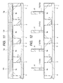
- FIG. 1 is a cross-sectional view of a part of a semiconductor substrate, illustrating a step in the method of manufacturing a MISFET according to one embodiment of the present invention
- FIG. 2 is a cross-sectional view of a part of the semiconductor substrate, illustrating a subsequent step in the method of manufacturing the MISFET according to the one embodiment of the present invention
- FIG. 3 is a schematic diagram of a treatment apparatus to be used for manufacturing a MISFET according to one embodiment of the present invention
- FIG. 4 is a schematic diagram showing a side view of the etching chamber of the treatment apparatus shown in FIG. 3;
- FIG. 5 is a cross-sectional view of a part of the semiconductor substrate, illustrating a subsequent step in the method of manufacturing the MISFET according to the one embodiment of the present invention
- FIG. 6 is a cross-sectional view of a part of the semiconductor substrate, illustrating a subsequent step in the method of manufacturing the MISFET according to the one embodiment of the present invention
- FIG. 7 is a cross-sectional view of a part of the semiconductor substrate, illustrating a subsequent step in the method of manufacturing the MISFET according to the one embodiment of the present invention
- FIG. 8 is a cross-sectional view of a part of the semiconductor substrate, illustrating a subsequent step in the method of manufacturing the MISFET according to the one embodiment of the present invention
- FIG. 9 is a cross-sectional view of a part of the semiconductor substrate, illustrating a subsequent step in the method of manufacturing the MISFET according to the one embodiment of the present invention.
- FIG. 10 is a cross-sectional view of a part of the semiconductor substrate, illustrating a subsequent step in the method of manufacturing the MISFET according to the one embodiment of the present invention
- FIG. 11 is a cross-sectional view of a part of the semiconductor substrate, illustrating a subsequent step in the method of manufacturing the MISFET according to the one embodiment of the present invention
- FIG. 12 is a cross-sectional view of a part of the semiconductor substrate, illustrating a subsequent step in the method of manufacturing the MISFET according to the one embodiment of the present invention
- FIG. 14 is a cross-sectional view of a part of the semiconductor substrate, illustrating a subsequent step in the method of manufacturing the MISFET according to the one embodiment of the present invention
- FIG. 15 is a cross-sectional view of a part of the semiconductor substrate, illustrating a subsequent step in the method for manufacturing the MISFET according to the one embodiment of the present invention
- FIG. 16 is a cross-sectional view of a part of the semiconductor substrate, illustrating a subsequent step in the method for manufacturing the MISFET according to the one embodiment of the present invention
- FIG. 17 is a cross-sectional view of a part of the semiconductor substrate, illustrating a subsequent step in the method of manufacturing the MISFET according to the one embodiment of the present invention.
- FIG. 19 is a cross-sectional view of a part of the semiconductor substrate, illustrating a subsequent step in the method of manufacturing the MISFET according to the one embodiment of the present invention.
- FIG. 21 is a cross-sectional view of a part of the semiconductor substrate, illustrating a subsequent step in the method of manufacturing the MISFET according to the other embodiment of the present invention.
- FIG. 22 is a cross-sectional view of a part of the semiconductor substrate, illustrating a subsequent step in the method of manufacturing the MISFET according to the other embodiment of the present invention.
- FIG. 25 is a cross-sectional view of a part of the semiconductor substrate, illustrating a subsequent step in the method of manufacturing the MISFET according to the other embodiment of the present invention.
- FIG. 26 is a cross-sectional view of a part of the semiconductor substrate, according to the method of manufacturing the MISFET according to the other embodiment of the present invention.
- FIG. 27 is a cross-sectional view of a part of the semiconductor substrate, illustrating a subsequent step in the method of manufacturing the MISFET according to the other embodiment of the present invention.
- FIG. 28 is a cross-sectional view of a part of the semiconductor substrate, illustrating a subsequent step in the method of manufacturing the MISFET according to the other embodiment of the present invention.
- FIG. 29 is a cross-sectional view of a part of the semiconductor substrate, illustrating a subsequent step in the method of manufacturing the MISFET according to the other embodiment of the present invention.
- a MISFET constituting the internal circuit is operated at a low voltage from the viewpoint of reducing the power consumption of the circuit.
- the gate insulating film of the MISFET constituting the internal circuit is comprised of a thin insulating film.
- the gate insulating film is provided in the form of a thick insulating film.
- FIGS. 1 to 19 A method for use in manufacturing the CMOS-LSI of this embodiment will be described with reference to FIGS. 1 to 19 , step by step.
- the left-hand side region and the right-hand side region of each of the cross-sectional views (FIGS. 1, 2 , and 5 to 19 ) of a semiconductor substrate which illustrate the method of manufacturing the CMOS-LSI, represent the internal circuit region and the I/O region, respectively.
- an element isolation trench 2 is formed in a semiconductor substrate (referred to hereinafter as a substrate) 1 made of, for example, p-type single-crystal silicon having a specific resistance of about 1 to 10 ⁇ cm.
- the element isolation trench 2 is formed in the following manner.
- the substrate 1 within an element isolation region, is etched to form a trench.
- a silicon dioxide film 3 is deposited on the substrate 1 , including the inside of the trench, by a CVD method.
- the silicon dioxide film 3 outside the trench is removed by a chemical mechanical polishing method.
- the substrate 1 is thermally oxidized to form a thin silicon dioxide film 7 , having a thickness of not more than 10 nm, on its surface.
- boron is ion-implanted into a part of the substrate 1 via the silicon dioxide film 7
- phosphorus is ion-implanted into another part thereof.
- the substrate 1 is heat-treated to diffuse the impurities (boron and phosphorus) into the inside of the substrate 1 .
- a p-type well 4 is formed in an n-channel type MISFET formation region
- an n-type well 5 is formed in a p-channel type MISFET formation region.
- boron is ion-implanted into the surface of the p-type well 4 (channel formation region), and phosphorus is ion-implanted into the surface of the n-type well 5 (channel formation region) for controlling the threshold voltage of the MISFET.
- the substrate 1 in wafer form that has been transported into the treatment apparatus 100 is first accommodated in the loader 106 . Subsequently, gas replacement in the loader 106 is performed, and then the substrate 1 is fed into the etching chamber 101 via the transport system.
- the etching chamber 101 is made up of a chamber 202 , including a stage 201 for mounting the substrate 1 thereon, and a plasma generation unit 203 disposed outside the chamber 202 .
- a fluorine-containing gas, or a mixed gas of a fluorine-containing gas and hydrogen is supplied to the plasma generation unit 203 .
- the gas is then decomposed by a plasma formed by a microwave or the like, thereby to form a fluorine radical, or a fluorine radical and a hydrogen radical.
- the thin silicon dioxide film 7 that has been formed on the surface of the substrate 1 is decomposed and removed.
- the substrate 1 from which the silicon dioxide film 7 has been removed, is taken out from the etching chamber 101 and transported into the oxidizing treatment chamber 102 . Then, the surface of the substrate 1 is wet oxidized in the oxidizing treatment chamber 102 , thereby to form a silicon dioxide film 6 with a thickness of about 1 to 4 nm on the surface of the substrate 1 (the p-type well 4 , the n-type well 5 ), as shown in FIG. 6 .
- the resulting silicon dioxide film 6 is used as a part of the gate insulating film of the MISFET constituting the I/O circuit.
- the substrate 1 on which the silicon dioxide film 6 has been formed is taken out from the oxidizing treatment chamber 102 and transported into the nitriding treatment chamber 103 .
- the surface of the substrate 1 is then nitrided therein.
- the silicon dioxide film 6 is nitrided to form a silicon oxynitride film 8 .
- the nitriding treatment of the silicon dioxide film 6 is accomplished by, for example, supplying an ammonia (NH 3 ) gas into the nitriding treatment chamber 103 and quickly heating the substrate 1 up to about 900° C. by lamp annealing. It is also possible to perform the nitriding treatment by a plasma treatment using nitrogen as a source gas. In such a case, by using the etching chamber 101 , wherein the chamber 202 for accommodating the substrate 1 therein is separated from the plasma generation unit 203 for generating a plasma, it is possible to reduce the damage to the substrate 1 due to the plasma.
- the foregoing nitriding treatment is not an essential step.
- the interface with a high dielectric film to be deposited on top of the silicon oxynitride film 8 in the subsequent step advantageously becomes less susceptible to oxidation.
- the substrate 1 on which the silicon oxynitride film 8 has been formed, is taken out from the nitriding treatment chamber 103 and transported into the exposing treatment chamber 104 . Then, as shown in FIG. 8, a part of the surface (I/O circuit region) of the substrate 1 is covered with a photoresist film 40 .
- a resist coating apparatus for spin-coating the surface of the substrate 1 with the photoresist film 40
- an exposing apparatus for transferring a prescribed pattern onto the photoresist film 40 that has been coated on the surface of the substrate 1
- a developing apparatus for developing the photoresist film 40 after completion of the exposing treatment
- an ashing apparatus for removing the photoresist film 40 on the surface of the substrate 1 .
- the substrate 1 on which the photoresist film 40 has been formed, is taken out from the exposing treatment chamber 104 and transported into the etching chamber 101 .
- the silicon oxynitride film 8 in the region not covered with the photoresist film 40 (the internal circuit region) is then removed.
- the substrate 1 is transported from the etching chamber 101 to the exposing treatment chamber 104 , and the photoresist film 40 is removed by an ashing treatment. Thereafter, the resulting substrate 1 is transported into the film-forming treatment chamber 105 . Then, as shown in FIG. 10, a high dielectric film 9 , with a thickness in terms of silicon dioxide of about 2 nm to 5 nm, is deposited on the substrate 1 .
- the resulting high dielectric film 9 is used as a gate insulating film of a MISFET constituting the internal circuit, and it is also used as a part of another gate insulating film of a MISFET constituting the I/O circuit.
- the high dielectric film 9 is a film made of a material having a larger relative dielectric constant than that of silicon nitride. More specifically, it is a film made of a material having a relative dielectric constant of not less than 8.0. Examples of a material having such a high relative dielectric constant may include titanium dioxide (TiO 2 ), hafnium dioxide (HfO 2 ), alumina (Al 2 O 3 ), zirconium dioxide (ZrO 2 ), and ruthenium dioxide (RuO 2 ).
- the high dielectric film 9 is a titanium dioxide film
- deposition is performed by a CVD method (deposition temperature, about 400° C.) using tetraisopropoxy titanium (Ti(iso-OC 3 H 7 ) 4 ) and oxygen as source gases.
- a high (ferro) dielectric film made of the foregoing metal oxide has crystal defects, such as oxygen loss, in the film immediately after deposition. For this reason, if it is used as a gate insulating film as it is, the gate withstand voltage may be reduced, or the leakage current may be increased.
- a heat treatment for modifying and crystallizing the dielectric film 9 is performed. This heat treatment is performed in the following manner. First, the substrate 1 is transported into the oxidizing treatment chamber 102 , and the substrate 1 is heat-treated in a high-temperature atmosphere containing oxygen.
- the substrate 1 is transported into the nitriding treatment chamber 103 , and the substrate 1 is heat-treated in a high-temperature atmosphere containing nitrogen.
- the heat treatment in the oxidizing treatment chamber 102 is performed at a temperature that is reduced to as low a level as possible.
- a thin gate insulating film 9 a comprised of the high dielectric film 9
- a thick gate insulating film 9 b comprised of a laminated film of the silicon oxynitride film 8 and the high dielectric film 9 , is formed on the surface of the substrate 1 in the I/O region.
- the foregoing treatment apparatus 100 is used, and a continuous treatment is performed without exposing the substrate 1 to air.
- a continuous treatment is performed without exposing the substrate 1 to air.
- an n-type polycrystal silicon film 10 n is formed on top of the p-type well 4
- a p-type polycrystal silicon film 10 p is formed on top of the n-type well 5 .
- These polycrystal silicon films ( 10 n and 10 p ) are used as gate electrode materials of the MISFETS.
- the polycrystal silicon films ( 10 n and 10 p ) are formed in the following manner.
- a non-doped polycrystal silicon film is deposited by a CVD method.
- phosphorus is doped into the polycrystal silicon film on top of the p-type well 4
- boron is doped into the polycrystal silicon film on top of the n-type well 5 by an ion implantation method using a photoresist film as a mask.
- the film-forming treatment chamber 105 of the treatment apparatus 100 may be used.
- a stand-alone CVD apparatus may also be used.
- the substrate 1 When deposition is performed in the film-forming treatment chamber 105 , the substrate 1 will not be exposed to air between the formation of the gate insulating films 9 a and 9 b and the deposition of the non-doped polycrystal silicon films. Therefore, it is possible to suppress the defects that result in undesired natural oxide films being formed on the surfaces of the gate insulating films 9 a and 9 b , and that result in foreign matter being deposited thereon.
- the gate electrode material may be comprised of a conductive film other than the foregoing polycrystal silicon films ( 10 n and 10 p ), such as a silicon film containing Ge (germanium) in an amount of several percent to several tens percent, a laminated film (polycide film) of a polycrystal silicon film and a refractory metal silicide film, or a laminated film (polymetal film) of a polycrystal silicon film and a refractory metal film.
- a conductive film other than the foregoing polycrystal silicon films ( 10 n and 10 p ) such as a silicon film containing Ge (germanium) in an amount of several percent to several tens percent, a laminated film (polycide film) of a polycrystal silicon film and a refractory metal silicide film, or a laminated film (polymetal film) of a polycrystal silicon film and a refractory metal film.
- the n-type polycrystal silicon film 10 n and the p-type polysilicon film 10 p are dry etched by using a photoresist film 41 as a mask.
- a gate electrode 11 n that is composed of the n-type polysilicon film 10 n
- a gate electrode 11 p that is composed of the p-type polycrystal silicon film 10 p
- n-type semiconductive regions 12 each with a low impurity concentration.
- boron is ion-implanted into the portions of the n-type well 5 on the opposite sides of the gate electrode 11 p to form p-type semiconductive regions 13 , each with a low impurity concentration.
- the n-type semiconductive region 12 is formed for rendering the n-channel type MISFET into a LDD (lightly doped drain) structure.
- the p-type semiconductive region 13 is formed for rendering the p-channel type MISFET into a LDD structure.
- sidewall spacers 14 are formed on the sidewalls of the gate electrodes 11 n and 11 p .
- the sidewall spacers 14 are formed in the following manner. A silicon nitride film is deposited on the substrate 1 by a CVD method. Subsequently, the resulting silicon nitride film is anisotropically etched so as to be partially left on the sidewalls of the gate electrodes 11 n and 11 p.
- phosphorus or arsenic is ion-implanted into the portions of the p-type well 4 on the opposite sides of the gate electrode 11 n .
- boron is ion-implanted into the portions of the n-type well 5 on the opposite sides of the gate electrode 11 p .
- the substrate 1 is heat-treated to diffuse the impurities therein.
- n + -type semiconductive regions (source and drain) 16 each having a high impurity concentration
- p + -type semiconductive regions (source and drain) 17 are formed in the n-type well 5 .
- the gate insulating films 9 a and 9 b that have been formed on top of the n + -type semiconductive regions (source and drain) 16 and the p + -type semiconductive regions (source and drain) 17 , respectively, are removed by etching.
- a cobalt (Co) film 18 a is deposited on the substrate 1 by a sputtering method.
- a Ti (titanium) film may also be deposited in place of the cobalt film 18 a.
- the cobalt film 18 a is allowed to react with silicon (the substrate 1 , and the gate electrodes 11 n and 11 p ). Then, the unreacted cobalt film 18 a is removed by wet etching. As a result, as shown in FIG. 16, cobalt silicide films 18 are formed on the respective surfaces of the n + -type semiconductive regions (source and drain) 16 , and the p + -type semiconductive regions (source and drain) 17 , and the gate electrodes 11 n and 11 p .
- the gate electrode 11 n or 11 p becomes a laminated film (polycide film) of the polycrystal silicon film ( 10 n or 10 p ) and the cobalt silicide film 18 .
- a silicon nitride film 19 is deposited on the substrate 1 by a CVD method.
- a silicon dioxide film 20 is deposited on top of the silicon nitride film 19 by a CVD method.
- the silicon dioxide film 20 and the underlying silicon nitride film 19 are dry etched by using a photoresist film 42 formed on top of the silicon dioxide film 20 as a mask.
- contact holes 21 are respectively formed on top of the n + -type semiconductive regions (source and drain) 16 and on top of the p + -type semiconductive regions (source and drain) 17 .
- the gate insulating film 9 b of the MISFETs (Qn 2 and QP 2 ) constituting the I/O circuit by use of a laminated film of the silicon oxynitride film 8 and the high dielectric film 9 , it is possible to ensure the reliability during high-voltage operation.
- an element isolation trench 2 is formed in a substrate 1 composed of p-type single-crystal silicon. Then, a silicon dioxide film 50 is deposited on the surface of the substrate 1 by a thermal oxidation method or a CVD method.
- a non-doped polycrystal silicon film that has been deposited on the substrate 1 by a CVD method, is patterned to form a dummy gate 51 in a region where a gate electrode will be formed.
- a silicon nitride film 55 and a silicon dioxide film 56 are sequentially deposited on the substrate 1 by a CVD method. Then, as shown in FIG. 24, a part of the silicon dioxide film 56 and a part of the underlying silicon nitride film 55 are removed by a chemical mechanical polishing method. As a consequence, the top face of the dummy gate 51 is exposed. Subsequently, as shown in FIG. 25, the dummy gate 51 is removed by etching.
- the resulting substrate 1 is transported into the etching chamber 101 of the treatment apparatus 100 shown in FIG. 3 .
- the silicon dioxide film 50 is etched in the region exposed by removal of the dummy gate 51 , so that the surface of the substrate 1 is exposed.
- the resulting substrate 1 is transported into the film-forming treatment chamber 105 of the treatment apparatus 100 .
- a high dielectric film 57 is deposited on the surface of the substrate 1 that has been exposed by the removal of the silicon dioxide film 50 and on the silicon dioxide film 56 .
- a W film 58 is deposited on top of the high dielectric film 57 .
- the resulting substrate 1 is transported out from the treatment apparatus 100 .
- the W film and the high dielectric film 57 on top of the silicon dioxide film 56 are removed by a chemical mechanical polishing method.
- a gate electrode 59 composed of the W film 58 is formed, and a gate insulating film 60 composed of the high dielectric film 57 is formed on the sidewall and the bottom of the gate electrode 59 .
- an n-channel type MISFET Qn 3 is formed on the substrate 1 .
- the steps from the removal of the silicon dioxide film 50 to the deposition of the W film 58 are continuously carried out in the treatment apparatus 100 .
- each gate insulating film of the MISFETs constituting the internal circuit is formed of a high dielectric film
- each gate insulating film of the MISFETs constituting the I/O circuit is formed of a laminated film of a silicon dioxide film (or a silicon oxynitride film) and a high dielectric film.
- the present invention is not limited thereto.
- each gate insulating film of a part of MISFETs is formed of a high dielectric film
- each gate insulating film of another part of the MISFETs is formed of a laminated film of a silicon dioxide film (or a silicon oxynitride film) and a high dielectric film.
- the present invention can also be applied to the case where a clean room wholly filled with an inert atmosphere is employed in place of the treatment apparatus 100 of the foregoing embodiments.
- the transport system and the loader/unloader units are filled with an inert atmosphere.
Abstract
Description
Claims (20)
Priority Applications (3)
| Application Number | Priority Date | Filing Date | Title |
|---|---|---|---|
| US10/699,690 US6909133B2 (en) | 2001-11-15 | 2003-11-04 | Method for manufacturing semiconductor integrated circuit device |
| US10/968,050 US7217607B2 (en) | 2001-11-15 | 2004-10-20 | Method for manufacturing semiconductor integrated circuit device |
| US11/738,741 US7655993B2 (en) | 2001-11-15 | 2007-04-23 | Method for manufacturing semiconductor integrated circuit device |
Applications Claiming Priority (2)
| Application Number | Priority Date | Filing Date | Title |
|---|---|---|---|
| JP2001-350636 | 2001-11-15 | ||
| JP2001350636A JP2003152102A (en) | 2001-11-15 | 2001-11-15 | Method of manufacturing semiconductor integrated circuit device |
Related Child Applications (1)
| Application Number | Title | Priority Date | Filing Date |
|---|---|---|---|
| US10/699,690 Division US6909133B2 (en) | 2001-11-15 | 2003-11-04 | Method for manufacturing semiconductor integrated circuit device |
Publications (2)
| Publication Number | Publication Date |
|---|---|
| US20030092233A1 US20030092233A1 (en) | 2003-05-15 |
| US6660597B2 true US6660597B2 (en) | 2003-12-09 |
Family
ID=19163096
Family Applications (4)
| Application Number | Title | Priority Date | Filing Date |
|---|---|---|---|
| US10/288,539 Expired - Lifetime US6660597B2 (en) | 2001-11-15 | 2002-11-06 | Method for manufacturing semiconductor integrated circuit device |
| US10/699,690 Expired - Lifetime US6909133B2 (en) | 2001-11-15 | 2003-11-04 | Method for manufacturing semiconductor integrated circuit device |
| US10/968,050 Expired - Fee Related US7217607B2 (en) | 2001-11-15 | 2004-10-20 | Method for manufacturing semiconductor integrated circuit device |
| US11/738,741 Expired - Fee Related US7655993B2 (en) | 2001-11-15 | 2007-04-23 | Method for manufacturing semiconductor integrated circuit device |
Family Applications After (3)
| Application Number | Title | Priority Date | Filing Date |
|---|---|---|---|
| US10/699,690 Expired - Lifetime US6909133B2 (en) | 2001-11-15 | 2003-11-04 | Method for manufacturing semiconductor integrated circuit device |
| US10/968,050 Expired - Fee Related US7217607B2 (en) | 2001-11-15 | 2004-10-20 | Method for manufacturing semiconductor integrated circuit device |
| US11/738,741 Expired - Fee Related US7655993B2 (en) | 2001-11-15 | 2007-04-23 | Method for manufacturing semiconductor integrated circuit device |
Country Status (5)
| Country | Link |
|---|---|
| US (4) | US6660597B2 (en) |
| JP (1) | JP2003152102A (en) |
| KR (1) | KR100904358B1 (en) |
| CN (1) | CN1301549C (en) |
| TW (1) | TWI291216B (en) |
Cited By (10)
| Publication number | Priority date | Publication date | Assignee | Title |
|---|---|---|---|---|
| US20040023459A1 (en) * | 2001-05-15 | 2004-02-05 | Nec Corporation | Semiconductor device including gate insulation films having different thicknesses |
| US20050009283A1 (en) * | 2003-07-07 | 2005-01-13 | Taiwan Semiconductor Manufacturing Company, Ltd. | Method for removal of a spacer |
| US20050064667A1 (en) * | 2003-09-19 | 2005-03-24 | Kabushiki Kaisha Toshiba | Semiconductor device manufacturing method |
| US20050077548A1 (en) * | 2001-11-15 | 2005-04-14 | Ryoichi Furukawa | Method for manufacturing semiconductor integrated circuit device |
| US20060215313A1 (en) * | 2005-03-25 | 2006-09-28 | Richard Hsiao | Method for using CVD process to encapsulate coil in a magnetic write head |
| US20060292782A1 (en) * | 2005-06-23 | 2006-12-28 | Fujitsu Limited | Semiconductor device and method for manufacturing the same |
| US20080304944A1 (en) * | 2007-06-06 | 2008-12-11 | Chien-Ming Sung | Preventing Contamination in Integrated Circuit Manufacturing Lines |
| US7582549B2 (en) | 2006-08-25 | 2009-09-01 | Micron Technology, Inc. | Atomic layer deposited barium strontium titanium oxide films |
| US20110124172A1 (en) * | 2009-11-24 | 2011-05-26 | Samsung Electronics Co., Ltd. | Method of forming insulating layer and method of manufacturing transistor using the same |
| US20150187659A1 (en) * | 2013-12-31 | 2015-07-02 | Texas Instruments Incorporated | High quality dielectric for hi-k last replacement gate transistors |
Families Citing this family (19)
| Publication number | Priority date | Publication date | Assignee | Title |
|---|---|---|---|---|
| JPWO2004017418A1 (en) * | 2002-08-15 | 2005-12-08 | 株式会社ルネサステクノロジ | Semiconductor integrated circuit device and manufacturing method thereof |
| JP2004158487A (en) * | 2002-11-01 | 2004-06-03 | Matsushita Electric Ind Co Ltd | Method of manufacturing semiconductor device |
| CN100352062C (en) * | 2003-10-30 | 2007-11-28 | 上海集成电路研发中心有限公司 | Grid structure from material with high dielectric constant and preparing technique |
| US7026203B2 (en) * | 2003-12-31 | 2006-04-11 | Dongbuanam Semiconductor Inc. | Method for forming dual gate electrodes using damascene gate process |
| JP4371092B2 (en) | 2004-12-14 | 2009-11-25 | セイコーエプソン株式会社 | Electrostatic actuator, droplet discharge head and method for manufacturing the same, droplet discharge apparatus and device |
| JP4588483B2 (en) * | 2005-02-21 | 2010-12-01 | ルネサスエレクトロニクス株式会社 | Semiconductor device |
| US7625824B2 (en) * | 2005-06-16 | 2009-12-01 | Oerlikon Usa, Inc. | Process change detection through the use of evolutionary algorithms |
| US7256464B2 (en) * | 2005-08-29 | 2007-08-14 | United Microelectronics Corp. | Metal oxide semiconductor transistor and fabrication method thereof |
| JP4991134B2 (en) * | 2005-09-15 | 2012-08-01 | ルネサスエレクトロニクス株式会社 | Semiconductor device and manufacturing method thereof |
| JP2007294082A (en) * | 2006-03-31 | 2007-11-08 | Semiconductor Energy Lab Co Ltd | Method for deleting data from nand type nonvolatile memory |
| JP5629120B2 (en) * | 2010-04-26 | 2014-11-19 | ルネサスエレクトロニクス株式会社 | Semiconductor device |
| US8889251B2 (en) * | 2011-02-09 | 2014-11-18 | Lawrence Livermore National Security, Llc. | Alkali resistant optical coatings for alkali lasers and methods of production thereof |
| US8674410B2 (en) * | 2012-03-07 | 2014-03-18 | Macronix International Co., Ltd. | Method of manufacturing metal silicide and semiconductor structure using the same |
| CN103531453B (en) * | 2012-07-02 | 2016-12-21 | 中芯国际集成电路制造(上海)有限公司 | Semiconductor integrated device and preparation method thereof |
| KR102020446B1 (en) | 2013-01-10 | 2019-09-10 | 삼성전자주식회사 | Method of forming an epitaxial layer, and apparatus and system for performing the same |
| CN104658899B (en) * | 2013-11-22 | 2017-11-10 | 中芯国际集成电路制造(上海)有限公司 | A kind of method for etching gate dielectric |
| CN104779146B (en) * | 2014-01-09 | 2017-11-14 | 中芯国际集成电路制造(上海)有限公司 | A kind of method for making semiconductor devices |
| CN108987249B (en) * | 2017-06-01 | 2021-08-17 | 无锡华润上华科技有限公司 | Method for forming cobalt silicide layer in semiconductor device |
| US20220162118A1 (en) * | 2020-11-23 | 2022-05-26 | Innolux Corporation | Method for preparing cover substrate |
Citations (3)
| Publication number | Priority date | Publication date | Assignee | Title |
|---|---|---|---|---|
| JP2000188338A (en) | 1998-12-21 | 2000-07-04 | Hitachi Ltd | Semiconductor device and its manufacture |
| US6165825A (en) * | 1997-03-28 | 2000-12-26 | Matsushita Electronics Corporation | Semiconductor device and method for producing the same |
| US6417052B1 (en) * | 1999-11-15 | 2002-07-09 | Hitachi, Ltd. | Fabrication process for semiconductor device |
Family Cites Families (33)
| Publication number | Priority date | Publication date | Assignee | Title |
|---|---|---|---|---|
| JPH07114241B2 (en) * | 1986-10-20 | 1995-12-06 | 松下電子工業株式会社 | Semiconductor device |
| JPH07109858B2 (en) * | 1988-04-07 | 1995-11-22 | 株式会社東芝 | Method for manufacturing semiconductor device |
| US5254489A (en) * | 1990-10-18 | 1993-10-19 | Nec Corporation | Method of manufacturing semiconductor device by forming first and second oxide films by use of nitridation |
| DE4304849C2 (en) * | 1992-02-21 | 2000-01-27 | Mitsubishi Electric Corp | Semiconductor device and method of manufacturing a semiconductor device |
| JP2666103B2 (en) * | 1992-06-03 | 1997-10-22 | カシオ計算機株式会社 | Thin film semiconductor device |
| JPH0758212A (en) * | 1993-08-19 | 1995-03-03 | Sony Corp | Cmos integrated circuit |
| US5480828A (en) * | 1994-09-30 | 1996-01-02 | Taiwan Semiconductor Manufacturing Corp. Ltd. | Differential gate oxide process by depressing or enhancing oxidation rate for mixed 3/5 V CMOS process |
| US6033943A (en) * | 1996-08-23 | 2000-03-07 | Advanced Micro Devices, Inc. | Dual gate oxide thickness integrated circuit and process for making same |
| US5926714A (en) * | 1996-12-03 | 1999-07-20 | Advanced Micro Devices, Inc. | Detached drain MOSFET |
| KR100220252B1 (en) * | 1996-12-28 | 1999-09-15 | 김영환 | Method of manufacturing semiconductor device |
| JP3967440B2 (en) * | 1997-12-09 | 2007-08-29 | 株式会社ルネサステクノロジ | Manufacturing method of semiconductor integrated circuit device |
| KR100253394B1 (en) * | 1997-12-29 | 2000-04-15 | 김영환 | Method for fabricating gate electrode having gate insulation film |
| KR100258880B1 (en) * | 1998-02-27 | 2000-06-15 | 김영환 | Method for manufacturing semiconductor device |
| JPH11330460A (en) | 1998-05-11 | 1999-11-30 | Toshiba Corp | Manufacture of semiconductor device |
| US6037222A (en) * | 1998-05-22 | 2000-03-14 | Taiwan Semiconductor Manufacturing Company | Method for fabricating a dual-gate dielectric module for memory embedded logic using salicide technology and polycide technology |
| US5960289A (en) * | 1998-06-22 | 1999-09-28 | Motorola, Inc. | Method for making a dual-thickness gate oxide layer using a nitride/oxide composite region |
| US6911707B2 (en) * | 1998-12-09 | 2005-06-28 | Advanced Micro Devices, Inc. | Ultrathin high-K gate dielectric with favorable interface properties for improved semiconductor device performance |
| JP2000307083A (en) | 1999-04-22 | 2000-11-02 | Hitachi Ltd | Semiconductor device and manufacture of the same |
| JP4149095B2 (en) | 1999-04-26 | 2008-09-10 | 株式会社ルネサステクノロジ | Manufacturing method of semiconductor integrated circuit device |
| JP2000349285A (en) | 1999-06-04 | 2000-12-15 | Hitachi Ltd | Manufacture of semiconductor integrated circuit device and the semiconductor integrated circuit device |
| JP2001127280A (en) | 1999-10-25 | 2001-05-11 | Sony Corp | Method for manufacturing semiconductor device and p- channel type semiconductor device |
| JP2001217415A (en) | 2000-01-31 | 2001-08-10 | Matsushita Electric Ind Co Ltd | Method for manufacturing semiconductor device |
| US6407435B1 (en) * | 2000-02-11 | 2002-06-18 | Sharp Laboratories Of America, Inc. | Multilayer dielectric stack and method |
| JP2001267591A (en) | 2000-03-14 | 2001-09-28 | Nec Corp | Shielding structure for optical unit for optical communication |
| JP2001284463A (en) | 2000-03-30 | 2001-10-12 | Nec Corp | Semiconductor device and method of manufacturing it |
| TW552672B (en) * | 2000-04-04 | 2003-09-11 | Agere Syst Guardian Corp | Dual gate semiconductor device having a nitrogen and oxygen containing barrier layer and a method of manufacture therefor |
| JP2001298095A (en) | 2000-04-13 | 2001-10-26 | Nec Corp | Method of manufacturing mos semiconductor device |
| JP2001308198A (en) * | 2000-04-27 | 2001-11-02 | Ricoh Co Ltd | Manufacturing method of semiconductor device |
| US6383873B1 (en) * | 2000-05-18 | 2002-05-07 | Motorola, Inc. | Process for forming a structure |
| US6524910B1 (en) * | 2000-09-27 | 2003-02-25 | Chartered Semiconductor Manufacturing Ltd. | Method of forming dual thickness gate dielectric structures via use of silicon nitride layers |
| US6562718B1 (en) * | 2000-12-06 | 2003-05-13 | Advanced Micro Devices, Inc. | Process for forming fully silicided gates |
| US6713846B1 (en) * | 2001-01-26 | 2004-03-30 | Aviza Technology, Inc. | Multilayer high κ dielectric films |
| JP2003152102A (en) * | 2001-11-15 | 2003-05-23 | Hitachi Ltd | Method of manufacturing semiconductor integrated circuit device |
-
2001
- 2001-11-15 JP JP2001350636A patent/JP2003152102A/en active Pending
-
2002
- 2002-10-29 TW TW091132063A patent/TWI291216B/en not_active IP Right Cessation
- 2002-11-06 US US10/288,539 patent/US6660597B2/en not_active Expired - Lifetime
- 2002-11-14 KR KR1020020070616A patent/KR100904358B1/en active IP Right Grant
- 2002-11-15 CN CNB021514046A patent/CN1301549C/en not_active Expired - Fee Related
-
2003
- 2003-11-04 US US10/699,690 patent/US6909133B2/en not_active Expired - Lifetime
-
2004
- 2004-10-20 US US10/968,050 patent/US7217607B2/en not_active Expired - Fee Related
-
2007
- 2007-04-23 US US11/738,741 patent/US7655993B2/en not_active Expired - Fee Related
Patent Citations (3)
| Publication number | Priority date | Publication date | Assignee | Title |
|---|---|---|---|---|
| US6165825A (en) * | 1997-03-28 | 2000-12-26 | Matsushita Electronics Corporation | Semiconductor device and method for producing the same |
| JP2000188338A (en) | 1998-12-21 | 2000-07-04 | Hitachi Ltd | Semiconductor device and its manufacture |
| US6417052B1 (en) * | 1999-11-15 | 2002-07-09 | Hitachi, Ltd. | Fabrication process for semiconductor device |
Cited By (24)
| Publication number | Priority date | Publication date | Assignee | Title |
|---|---|---|---|---|
| US6798027B2 (en) * | 2001-05-15 | 2004-09-28 | Nec Electronics Corporation | Semiconductor device including gate insulation films having different thicknesses |
| US20040023459A1 (en) * | 2001-05-15 | 2004-02-05 | Nec Corporation | Semiconductor device including gate insulation films having different thicknesses |
| US20050077548A1 (en) * | 2001-11-15 | 2005-04-14 | Ryoichi Furukawa | Method for manufacturing semiconductor integrated circuit device |
| US7217607B2 (en) * | 2001-11-15 | 2007-05-15 | Renesas Technology Corp. | Method for manufacturing semiconductor integrated circuit device |
| US20070187764A1 (en) * | 2001-11-15 | 2007-08-16 | Ryoichi Furukawa | Method for manufacturing semiconductor integrated circuit device |
| US7655993B2 (en) | 2001-11-15 | 2010-02-02 | Renesas Technology Corporation | Method for manufacturing semiconductor integrated circuit device |
| US20050009283A1 (en) * | 2003-07-07 | 2005-01-13 | Taiwan Semiconductor Manufacturing Company, Ltd. | Method for removal of a spacer |
| US20050064667A1 (en) * | 2003-09-19 | 2005-03-24 | Kabushiki Kaisha Toshiba | Semiconductor device manufacturing method |
| US7816215B2 (en) * | 2003-09-19 | 2010-10-19 | Kabushiki Kaisha Toshiba | Semiconductor device manufacturing method |
| US7627942B2 (en) * | 2005-03-25 | 2009-12-08 | Hitachi Global Storage Technologies Netherlands B.V. | Method for using CVD process to encapsulate coil in a magnetic write head |
| US20060215313A1 (en) * | 2005-03-25 | 2006-09-28 | Richard Hsiao | Method for using CVD process to encapsulate coil in a magnetic write head |
| US20060292782A1 (en) * | 2005-06-23 | 2006-12-28 | Fujitsu Limited | Semiconductor device and method for manufacturing the same |
| US7768039B2 (en) | 2005-06-23 | 2010-08-03 | Fujitsu Semiconductor Limited | Field effect transistors with different gate widths |
| US20100255668A1 (en) * | 2005-06-23 | 2010-10-07 | Fujitsu Microelectronics Limited | Field effect transistors with different gate widths |
| US7927941B2 (en) | 2005-06-23 | 2011-04-19 | Fujitsu Semiconductor Limited | Method of fabricating field effect transistors with different gate widths |
| US7582549B2 (en) | 2006-08-25 | 2009-09-01 | Micron Technology, Inc. | Atomic layer deposited barium strontium titanium oxide films |
| US8581352B2 (en) | 2006-08-25 | 2013-11-12 | Micron Technology, Inc. | Electronic devices including barium strontium titanium oxide films |
| US9202686B2 (en) | 2006-08-25 | 2015-12-01 | Micron Technology, Inc. | Electronic devices including barium strontium titanium oxide films |
| US20080304944A1 (en) * | 2007-06-06 | 2008-12-11 | Chien-Ming Sung | Preventing Contamination in Integrated Circuit Manufacturing Lines |
| US9177843B2 (en) * | 2007-06-06 | 2015-11-03 | Taiwan Semiconductor Manufacturing Company, Ltd. | Preventing contamination in integrated circuit manufacturing lines |
| US20110124172A1 (en) * | 2009-11-24 | 2011-05-26 | Samsung Electronics Co., Ltd. | Method of forming insulating layer and method of manufacturing transistor using the same |
| US8183136B2 (en) * | 2009-11-24 | 2012-05-22 | Samsung Electronics Co., Ltd. | Method of forming insulating layer and method of manufacturing transistor using the same |
| US20150187659A1 (en) * | 2013-12-31 | 2015-07-02 | Texas Instruments Incorporated | High quality dielectric for hi-k last replacement gate transistors |
| US9269636B2 (en) * | 2013-12-31 | 2016-02-23 | Texas Instruments Incorporated | High quality dielectric for hi-k last replacement gate transistors |
Also Published As
| Publication number | Publication date |
|---|---|
| JP2003152102A (en) | 2003-05-23 |
| US20040106289A1 (en) | 2004-06-03 |
| KR100904358B1 (en) | 2009-06-23 |
| US6909133B2 (en) | 2005-06-21 |
| US7655993B2 (en) | 2010-02-02 |
| US20070187764A1 (en) | 2007-08-16 |
| US7217607B2 (en) | 2007-05-15 |
| KR20030040162A (en) | 2003-05-22 |
| US20050077548A1 (en) | 2005-04-14 |
| US20030092233A1 (en) | 2003-05-15 |
| CN1420548A (en) | 2003-05-28 |
| TWI291216B (en) | 2007-12-11 |
| CN1301549C (en) | 2007-02-21 |
| TW200301957A (en) | 2003-07-16 |
Similar Documents
| Publication | Publication Date | Title |
|---|---|---|
| US7655993B2 (en) | Method for manufacturing semiconductor integrated circuit device | |
| US6451647B1 (en) | Integrated plasma etch of gate and gate dielectric and low power plasma post gate etch removal of high-K residual | |
| US6797599B2 (en) | Gate structure and method | |
| KR100623584B1 (en) | Dual-gate structure and method of fabricating integrated circuits having dual-gate structures | |
| US6764898B1 (en) | Implantation into high-K dielectric material after gate etch to facilitate removal | |
| US6909156B2 (en) | Semiconductor device and manufacturing method therefor | |
| US20070210354A1 (en) | Semiconductor device and semiconductor device manufacturing method | |
| US20080001237A1 (en) | Semiconductor device having nitrided high-k gate dielectric and metal gate electrode and methods of forming same | |
| JP2005150737A (en) | Semiconductor element having different types of gate insulating films and method for manufacturing the same | |
| JP2011077421A (en) | Method of manufacturing semiconductor device | |
| US6586293B1 (en) | Semiconductor device and method of manufacturing the same | |
| KR20210110734A (en) | Vertical Transistor Fabrication for Memory Applications | |
| US8557651B2 (en) | Method of manufacturing a semiconductor device using an etchant | |
| JP2002359371A (en) | Semiconductor device and its manufacturing method | |
| US7306985B2 (en) | Method for manufacturing semiconductor device including heat treating with a flash lamp | |
| US9786762B2 (en) | Gate electrode of a semiconductor device, and method for producing same | |
| JP5050351B2 (en) | Manufacturing method of semiconductor device | |
| JP2004079931A (en) | Manufacturing method for semiconductor device | |
| JP2010021200A (en) | Method for manufacturing semiconductor device | |
| KR100814372B1 (en) | Method of manufacturing a semiconductor device | |
| JP2006128416A (en) | Semiconductor apparatus and its manufacturing method | |
| KR100529472B1 (en) | Method of forming a transistor using a dielectric | |
| JP4532925B2 (en) | Semiconductor device manufacturing method and semiconductor device | |
| US6905971B1 (en) | Treatment of dielectric material to enhance etch rate | |
| JP4951585B2 (en) | Manufacturing method of semiconductor integrated circuit device |
Legal Events
| Date | Code | Title | Description |
|---|---|---|---|
| AS | Assignment |
Owner name: HITACHI, LTD., JAPAN Free format text: ASSIGNMENT OF ASSIGNORS INTEREST;ASSIGNORS:FURUKAWA, RYOICHI;SAKAI, SATOSHI;YAMAMOTO, SATOSHI;REEL/FRAME:013465/0755;SIGNING DATES FROM 20020920 TO 20020924 |
|
| AS | Assignment |
Owner name: RENESAS TECHNOLOGY CORPORATION, JAPAN Free format text: ASSIGNMENT OF ASSIGNORS INTEREST;ASSIGNOR:HITACHI, LTD.;REEL/FRAME:014569/0585 Effective date: 20030912 |
|
| STCF | Information on status: patent grant |
Free format text: PATENTED CASE |
|
| FEPP | Fee payment procedure |
Free format text: PAYOR NUMBER ASSIGNED (ORIGINAL EVENT CODE: ASPN); ENTITY STATUS OF PATENT OWNER: LARGE ENTITY |
|
| FPAY | Fee payment |
Year of fee payment: 4 |
|
| AS | Assignment |
Owner name: RENESAS ELECTRONICS CORPORATION, JAPAN Free format text: MERGER;ASSIGNOR:RENESAS TECHNOLOGY CORP.;REEL/FRAME:025204/0512 Effective date: 20100401 |
|
| FPAY | Fee payment |
Year of fee payment: 8 |
|
| FPAY | Fee payment |
Year of fee payment: 12 |
|
| AS | Assignment |
Owner name: RENESAS ELECTRONICS CORPORATION, JAPAN Free format text: CHANGE OF ADDRESS;ASSIGNOR:RENESAS ELECTRONICS CORPORATION;REEL/FRAME:044928/0001 Effective date: 20150806 |