US6614079B2 - All-in-one disposable/permanent spacer elevated source/drain, self-aligned silicide CMOS - Google Patents
All-in-one disposable/permanent spacer elevated source/drain, self-aligned silicide CMOS Download PDFInfo
- Publication number
- US6614079B2 US6614079B2 US09/909,307 US90930701A US6614079B2 US 6614079 B2 US6614079 B2 US 6614079B2 US 90930701 A US90930701 A US 90930701A US 6614079 B2 US6614079 B2 US 6614079B2
- Authority
- US
- United States
- Prior art keywords
- regions
- semiconductor substrate
- cmos device
- gate stack
- spacer
- Prior art date
- Legal status (The legal status is an assumption and is not a legal conclusion. Google has not performed a legal analysis and makes no representation as to the accuracy of the status listed.)
- Expired - Lifetime
Links
- 229910021332 silicide Inorganic materials 0.000 title claims abstract description 40
- FVBUAEGBCNSCDD-UHFFFAOYSA-N silicide(4-) Chemical compound [Si-4] FVBUAEGBCNSCDD-UHFFFAOYSA-N 0.000 title claims abstract description 38
- 125000006850 spacer group Chemical group 0.000 title claims description 33
- 239000000758 substrate Substances 0.000 claims abstract description 56
- 239000004065 semiconductor Substances 0.000 claims abstract description 46
- 229910044991 metal oxide Inorganic materials 0.000 claims abstract description 5
- 150000004706 metal oxides Chemical class 0.000 claims abstract description 5
- 230000000295 complement effect Effects 0.000 claims abstract description 4
- 150000004767 nitrides Chemical class 0.000 claims description 30
- 125000001475 halogen functional group Chemical group 0.000 claims description 28
- 239000007943 implant Substances 0.000 claims description 28
- 239000000463 material Substances 0.000 claims description 19
- 229910052751 metal Inorganic materials 0.000 claims description 13
- 239000002184 metal Substances 0.000 claims description 13
- VYPSYNLAJGMNEJ-UHFFFAOYSA-N Silicium dioxide Chemical compound O=[Si]=O VYPSYNLAJGMNEJ-UHFFFAOYSA-N 0.000 claims description 7
- 229910052710 silicon Inorganic materials 0.000 claims description 7
- 229910021420 polycrystalline silicon Inorganic materials 0.000 claims description 6
- 229920005591 polysilicon Polymers 0.000 claims description 6
- 229910000577 Silicon-germanium Inorganic materials 0.000 claims description 4
- MCMNRKCIXSYSNV-UHFFFAOYSA-N Zirconium dioxide Chemical compound O=[Zr]=O MCMNRKCIXSYSNV-UHFFFAOYSA-N 0.000 claims description 4
- 229910021417 amorphous silicon Inorganic materials 0.000 claims description 4
- 150000002739 metals Chemical class 0.000 claims description 4
- 229910052581 Si3N4 Inorganic materials 0.000 claims description 3
- 229910052681 coesite Inorganic materials 0.000 claims description 3
- 229910052906 cristobalite Inorganic materials 0.000 claims description 3
- 239000012212 insulator Substances 0.000 claims description 3
- 239000000377 silicon dioxide Substances 0.000 claims description 3
- 229910052682 stishovite Inorganic materials 0.000 claims description 3
- 229910052905 tridymite Inorganic materials 0.000 claims description 3
- 206010010144 Completed suicide Diseases 0.000 claims description 2
- 229910001218 Gallium arsenide Inorganic materials 0.000 claims description 2
- 229910000673 Indium arsenide Inorganic materials 0.000 claims description 2
- 229910045601 alloy Inorganic materials 0.000 claims description 2
- 239000000956 alloy Substances 0.000 claims description 2
- PNEYBMLMFCGWSK-UHFFFAOYSA-N aluminium oxide Inorganic materials [O-2].[O-2].[O-2].[Al+3].[Al+3] PNEYBMLMFCGWSK-UHFFFAOYSA-N 0.000 claims description 2
- 229910052593 corundum Inorganic materials 0.000 claims description 2
- 229910052732 germanium Inorganic materials 0.000 claims description 2
- CJNBYAVZURUTKZ-UHFFFAOYSA-N hafnium(IV) oxide Inorganic materials O=[Hf]=O CJNBYAVZURUTKZ-UHFFFAOYSA-N 0.000 claims description 2
- RPQDHPTXJYYUPQ-UHFFFAOYSA-N indium arsenide Chemical compound [In]#[As] RPQDHPTXJYYUPQ-UHFFFAOYSA-N 0.000 claims description 2
- -1 silicon, elemental metals Chemical class 0.000 claims description 2
- PBCFLUZVCVVTBY-UHFFFAOYSA-N tantalum pentoxide Inorganic materials O=[Ta](=O)O[Ta](=O)=O PBCFLUZVCVVTBY-UHFFFAOYSA-N 0.000 claims description 2
- 229910001845 yogo sapphire Inorganic materials 0.000 claims description 2
- 238000004519 manufacturing process Methods 0.000 abstract description 5
- 238000000034 method Methods 0.000 description 49
- 239000002019 doping agent Substances 0.000 description 12
- 238000005530 etching Methods 0.000 description 12
- 238000005468 ion implantation Methods 0.000 description 12
- 230000015572 biosynthetic process Effects 0.000 description 11
- 238000000137 annealing Methods 0.000 description 10
- 239000002131 composite material Substances 0.000 description 10
- 239000003989 dielectric material Substances 0.000 description 8
- 238000013459 approach Methods 0.000 description 7
- 230000004913 activation Effects 0.000 description 6
- 238000005137 deposition process Methods 0.000 description 6
- 238000005229 chemical vapour deposition Methods 0.000 description 5
- 238000000151 deposition Methods 0.000 description 5
- 238000009792 diffusion process Methods 0.000 description 5
- 229920002120 photoresistant polymer Polymers 0.000 description 5
- 239000003870 refractory metal Substances 0.000 description 5
- 230000003213 activating effect Effects 0.000 description 4
- 239000000126 substance Substances 0.000 description 4
- 230000008021 deposition Effects 0.000 description 3
- 229910052738 indium Inorganic materials 0.000 description 3
- 238000001020 plasma etching Methods 0.000 description 3
- 238000000623 plasma-assisted chemical vapour deposition Methods 0.000 description 3
- 230000004888 barrier function Effects 0.000 description 2
- 238000000224 chemical solution deposition Methods 0.000 description 2
- 239000004020 conductor Substances 0.000 description 2
- 238000001704 evaporation Methods 0.000 description 2
- 230000008020 evaporation Effects 0.000 description 2
- 238000002513 implantation Methods 0.000 description 2
- 238000001459 lithography Methods 0.000 description 2
- 230000003647 oxidation Effects 0.000 description 2
- 238000007254 oxidation reaction Methods 0.000 description 2
- 238000000059 patterning Methods 0.000 description 2
- 230000001052 transient effect Effects 0.000 description 2
- 229910052721 tungsten Inorganic materials 0.000 description 2
- 229910000531 Co alloy Inorganic materials 0.000 description 1
- NBIIXXVUZAFLBC-UHFFFAOYSA-N Phosphoric acid Chemical compound OP(O)(O)=O NBIIXXVUZAFLBC-UHFFFAOYSA-N 0.000 description 1
- XUIMIQQOPSSXEZ-UHFFFAOYSA-N Silicon Chemical compound [Si] XUIMIQQOPSSXEZ-UHFFFAOYSA-N 0.000 description 1
- 229910004200 TaSiN Inorganic materials 0.000 description 1
- ATJFFYVFTNAWJD-UHFFFAOYSA-N Tin Chemical compound [Sn] ATJFFYVFTNAWJD-UHFFFAOYSA-N 0.000 description 1
- 229910052782 aluminium Inorganic materials 0.000 description 1
- 150000001875 compounds Chemical class 0.000 description 1
- 238000001312 dry etching Methods 0.000 description 1
- 230000000694 effects Effects 0.000 description 1
- 230000005669 field effect Effects 0.000 description 1
- 229910052735 hafnium Inorganic materials 0.000 description 1
- 238000010884 ion-beam technique Methods 0.000 description 1
- 229910052741 iridium Inorganic materials 0.000 description 1
- 238000002955 isolation Methods 0.000 description 1
- 238000000608 laser ablation Methods 0.000 description 1
- 229910001092 metal group alloy Inorganic materials 0.000 description 1
- 229910052759 nickel Inorganic materials 0.000 description 1
- 229910052763 palladium Inorganic materials 0.000 description 1
- 238000007747 plating Methods 0.000 description 1
- 229910052697 platinum Inorganic materials 0.000 description 1
- 230000005855 radiation Effects 0.000 description 1
- 238000004151 rapid thermal annealing Methods 0.000 description 1
- 239000000376 reactant Substances 0.000 description 1
- 238000010405 reoxidation reaction Methods 0.000 description 1
- 229910052703 rhodium Inorganic materials 0.000 description 1
- 229910052707 ruthenium Inorganic materials 0.000 description 1
- 239000010703 silicon Substances 0.000 description 1
- 229910052814 silicon oxide Inorganic materials 0.000 description 1
- 229910052715 tantalum Inorganic materials 0.000 description 1
- 229910052719 titanium Inorganic materials 0.000 description 1
- 229910052726 zirconium Inorganic materials 0.000 description 1
Images


Classifications
-
- H—ELECTRICITY
- H01—ELECTRIC ELEMENTS
- H01L—SEMICONDUCTOR DEVICES NOT COVERED BY CLASS H10
- H01L29/00—Semiconductor devices adapted for rectifying, amplifying, oscillating or switching, or capacitors or resistors with at least one potential-jump barrier or surface barrier, e.g. PN junction depletion layer or carrier concentration layer; Details of semiconductor bodies or of electrodes thereof ; Multistep manufacturing processes therefor
- H01L29/66—Types of semiconductor device ; Multistep manufacturing processes therefor
- H01L29/66007—Multistep manufacturing processes
- H01L29/66075—Multistep manufacturing processes of devices having semiconductor bodies comprising group 14 or group 13/15 materials
- H01L29/66227—Multistep manufacturing processes of devices having semiconductor bodies comprising group 14 or group 13/15 materials the devices being controllable only by the electric current supplied or the electric potential applied, to an electrode which does not carry the current to be rectified, amplified or switched, e.g. three-terminal devices
- H01L29/66409—Unipolar field-effect transistors
- H01L29/66477—Unipolar field-effect transistors with an insulated gate, i.e. MISFET
- H01L29/6653—Unipolar field-effect transistors with an insulated gate, i.e. MISFET using the removal of at least part of spacer, e.g. disposable spacer
-
- H—ELECTRICITY
- H01—ELECTRIC ELEMENTS
- H01L—SEMICONDUCTOR DEVICES NOT COVERED BY CLASS H10
- H01L21/00—Processes or apparatus adapted for the manufacture or treatment of semiconductor or solid state devices or of parts thereof
- H01L21/70—Manufacture or treatment of devices consisting of a plurality of solid state components formed in or on a common substrate or of parts thereof; Manufacture of integrated circuit devices or of parts thereof
- H01L21/77—Manufacture or treatment of devices consisting of a plurality of solid state components or integrated circuits formed in, or on, a common substrate
- H01L21/78—Manufacture or treatment of devices consisting of a plurality of solid state components or integrated circuits formed in, or on, a common substrate with subsequent division of the substrate into plural individual devices
- H01L21/82—Manufacture or treatment of devices consisting of a plurality of solid state components or integrated circuits formed in, or on, a common substrate with subsequent division of the substrate into plural individual devices to produce devices, e.g. integrated circuits, each consisting of a plurality of components
- H01L21/822—Manufacture or treatment of devices consisting of a plurality of solid state components or integrated circuits formed in, or on, a common substrate with subsequent division of the substrate into plural individual devices to produce devices, e.g. integrated circuits, each consisting of a plurality of components the substrate being a semiconductor, using silicon technology
- H01L21/8232—Field-effect technology
- H01L21/8234—MIS technology, i.e. integration processes of field effect transistors of the conductor-insulator-semiconductor type
- H01L21/823418—MIS technology, i.e. integration processes of field effect transistors of the conductor-insulator-semiconductor type with a particular manufacturing method of the source or drain structures, e.g. specific source or drain implants or silicided source or drain structures or raised source or drain structures
- H01L21/823425—MIS technology, i.e. integration processes of field effect transistors of the conductor-insulator-semiconductor type with a particular manufacturing method of the source or drain structures, e.g. specific source or drain implants or silicided source or drain structures or raised source or drain structures manufacturing common source or drain regions between a plurality of conductor-insulator-semiconductor structures
-
- H—ELECTRICITY
- H01—ELECTRIC ELEMENTS
- H01L—SEMICONDUCTOR DEVICES NOT COVERED BY CLASS H10
- H01L21/00—Processes or apparatus adapted for the manufacture or treatment of semiconductor or solid state devices or of parts thereof
- H01L21/70—Manufacture or treatment of devices consisting of a plurality of solid state components formed in or on a common substrate or of parts thereof; Manufacture of integrated circuit devices or of parts thereof
- H01L21/77—Manufacture or treatment of devices consisting of a plurality of solid state components or integrated circuits formed in, or on, a common substrate
- H01L21/78—Manufacture or treatment of devices consisting of a plurality of solid state components or integrated circuits formed in, or on, a common substrate with subsequent division of the substrate into plural individual devices
- H01L21/82—Manufacture or treatment of devices consisting of a plurality of solid state components or integrated circuits formed in, or on, a common substrate with subsequent division of the substrate into plural individual devices to produce devices, e.g. integrated circuits, each consisting of a plurality of components
- H01L21/822—Manufacture or treatment of devices consisting of a plurality of solid state components or integrated circuits formed in, or on, a common substrate with subsequent division of the substrate into plural individual devices to produce devices, e.g. integrated circuits, each consisting of a plurality of components the substrate being a semiconductor, using silicon technology
- H01L21/8232—Field-effect technology
- H01L21/8234—MIS technology, i.e. integration processes of field effect transistors of the conductor-insulator-semiconductor type
- H01L21/8238—Complementary field-effect transistors, e.g. CMOS
- H01L21/823814—Complementary field-effect transistors, e.g. CMOS with a particular manufacturing method of the source or drain structures, e.g. specific source or drain implants or silicided source or drain structures or raised source or drain structures
-
- H—ELECTRICITY
- H01—ELECTRIC ELEMENTS
- H01L—SEMICONDUCTOR DEVICES NOT COVERED BY CLASS H10
- H01L29/00—Semiconductor devices adapted for rectifying, amplifying, oscillating or switching, or capacitors or resistors with at least one potential-jump barrier or surface barrier, e.g. PN junction depletion layer or carrier concentration layer; Details of semiconductor bodies or of electrodes thereof ; Multistep manufacturing processes therefor
- H01L29/66—Types of semiconductor device ; Multistep manufacturing processes therefor
- H01L29/66007—Multistep manufacturing processes
- H01L29/66075—Multistep manufacturing processes of devices having semiconductor bodies comprising group 14 or group 13/15 materials
- H01L29/66227—Multistep manufacturing processes of devices having semiconductor bodies comprising group 14 or group 13/15 materials the devices being controllable only by the electric current supplied or the electric potential applied, to an electrode which does not carry the current to be rectified, amplified or switched, e.g. three-terminal devices
- H01L29/66409—Unipolar field-effect transistors
- H01L29/66477—Unipolar field-effect transistors with an insulated gate, i.e. MISFET
- H01L29/6656—Unipolar field-effect transistors with an insulated gate, i.e. MISFET using multiple spacer layers, e.g. multiple sidewall spacers
-
- H—ELECTRICITY
- H01—ELECTRIC ELEMENTS
- H01L—SEMICONDUCTOR DEVICES NOT COVERED BY CLASS H10
- H01L29/00—Semiconductor devices adapted for rectifying, amplifying, oscillating or switching, or capacitors or resistors with at least one potential-jump barrier or surface barrier, e.g. PN junction depletion layer or carrier concentration layer; Details of semiconductor bodies or of electrodes thereof ; Multistep manufacturing processes therefor
- H01L29/66—Types of semiconductor device ; Multistep manufacturing processes therefor
- H01L29/66007—Multistep manufacturing processes
- H01L29/66075—Multistep manufacturing processes of devices having semiconductor bodies comprising group 14 or group 13/15 materials
- H01L29/66227—Multistep manufacturing processes of devices having semiconductor bodies comprising group 14 or group 13/15 materials the devices being controllable only by the electric current supplied or the electric potential applied, to an electrode which does not carry the current to be rectified, amplified or switched, e.g. three-terminal devices
- H01L29/66409—Unipolar field-effect transistors
- H01L29/66477—Unipolar field-effect transistors with an insulated gate, i.e. MISFET
- H01L29/66568—Lateral single gate silicon transistors
- H01L29/66575—Lateral single gate silicon transistors where the source and drain or source and drain extensions are self-aligned to the sides of the gate
- H01L29/6659—Lateral single gate silicon transistors where the source and drain or source and drain extensions are self-aligned to the sides of the gate with both lightly doped source and drain extensions and source and drain self-aligned to the sides of the gate, e.g. lightly doped drain [LDD] MOSFET, double diffused drain [DDD] MOSFET
-
- H—ELECTRICITY
- H01—ELECTRIC ELEMENTS
- H01L—SEMICONDUCTOR DEVICES NOT COVERED BY CLASS H10
- H01L29/00—Semiconductor devices adapted for rectifying, amplifying, oscillating or switching, or capacitors or resistors with at least one potential-jump barrier or surface barrier, e.g. PN junction depletion layer or carrier concentration layer; Details of semiconductor bodies or of electrodes thereof ; Multistep manufacturing processes therefor
- H01L29/66—Types of semiconductor device ; Multistep manufacturing processes therefor
- H01L29/66007—Multistep manufacturing processes
- H01L29/66075—Multistep manufacturing processes of devices having semiconductor bodies comprising group 14 or group 13/15 materials
- H01L29/66227—Multistep manufacturing processes of devices having semiconductor bodies comprising group 14 or group 13/15 materials the devices being controllable only by the electric current supplied or the electric potential applied, to an electrode which does not carry the current to be rectified, amplified or switched, e.g. three-terminal devices
- H01L29/66409—Unipolar field-effect transistors
- H01L29/66477—Unipolar field-effect transistors with an insulated gate, i.e. MISFET
- H01L29/66568—Lateral single gate silicon transistors
- H01L29/66613—Lateral single gate silicon transistors with a gate recessing step, e.g. using local oxidation
- H01L29/66628—Lateral single gate silicon transistors with a gate recessing step, e.g. using local oxidation recessing the gate by forming single crystalline semiconductor material at the source or drain location
-
- H—ELECTRICITY
- H01—ELECTRIC ELEMENTS
- H01L—SEMICONDUCTOR DEVICES NOT COVERED BY CLASS H10
- H01L29/00—Semiconductor devices adapted for rectifying, amplifying, oscillating or switching, or capacitors or resistors with at least one potential-jump barrier or surface barrier, e.g. PN junction depletion layer or carrier concentration layer; Details of semiconductor bodies or of electrodes thereof ; Multistep manufacturing processes therefor
- H01L29/66—Types of semiconductor device ; Multistep manufacturing processes therefor
- H01L29/68—Types of semiconductor device ; Multistep manufacturing processes therefor controllable by only the electric current supplied, or only the electric potential applied, to an electrode which does not carry the current to be rectified, amplified or switched
- H01L29/76—Unipolar devices, e.g. field effect transistors
- H01L29/772—Field effect transistors
- H01L29/78—Field effect transistors with field effect produced by an insulated gate
- H01L29/7833—Field effect transistors with field effect produced by an insulated gate with lightly doped drain or source extension, e.g. LDD MOSFET's; DDD MOSFET's
- H01L29/7834—Field effect transistors with field effect produced by an insulated gate with lightly doped drain or source extension, e.g. LDD MOSFET's; DDD MOSFET's with a non-planar structure, e.g. the gate or the source or the drain being non-planar
Definitions
- the present invention relates to complementary metal oxide semiconductor (CMOS) devices, and more particularly to a process and structure for forming a metal oxide semiconductor field effect transistor (MOSFET), wherein gate sidewall composite spacers, which are partially removed during device processing, are employed.
- CMOS complementary metal oxide semiconductor
- MOSFET metal oxide semiconductor field effect transistor
- the present invention thus provides a method to form low temperature silicide contacts that are self-aligned to the deep junction edges present in the device, while still achieving the lower thermal budget of a conventional disposable spacer process.
- CMOS technology becomes smaller and smaller, e.g., less than about 50 nm gate length, it becomes more and more difficult to improve the short channel device performance and at the same time maintain acceptable values for off-state leakage current.
- the extension regions near the channel must be abrupt, i.e., less than 4 nm/decade, but the halo profile in proximity to the extension junction must be abrupt, i.e., less than 20 nm/decade.
- halo formation is typically carried out by a general approach wherein the halo dopants are implanted at an angle ranging from 0° to about 70° into the channel region.
- This prior art approach varies either the dose, the type of halo dopant or angle of halo implants for improving device performance.
- None of the above cited prior art references provides a method of improving the abruptness of the halo dopant profiles in the area next to the channel.
- the halo implants will suffer enhanced transient diffusion during extension junction and high thermal budget deep source/drain rapid thermal annealing (typically on the order of about 1000° C. for about 5 seconds). Consequently, these much degraded halo implant regions severely compromise their usefulness for improving short channel device characteristics, which is especially the case for device channel widths below 50 nm.
- all the prior art approaches provide no means to minimize transient enhanced diffusion of the halo dopants and hence the prior art approaches are not capable of creating abrupt super-halo implants in the region next to the channel region.
- One object of the present invention is to provide a method of fabricating a complementary metal oxide semiconductor (CMOS) device that includes a low temperature silicide that is self-aligned to the deep junction edges present in the device.
- CMOS complementary metal oxide semiconductor
- Another object of the present invention is to provide a method wherein a low thermal budget is used in fabricating a CMOS device.
- a further object of the present invention is to provide a method of fabricating a CMOS device that includes a self-aligned silicide region that is formed without the need of a second spacer.
- a yet further object of the present invention is to fabricate a raised or non-raised source/drain (S/D) CMOS device, wherein all high temperature processes, such as source/drain anneals and selective epi growth, are performed prior to halo formation.
- S/D source/drain
- a still further object of the present invention is to provide a method of fabricating a CMOS device having abrupt junction profiles therein.
- the inventive method is capable of forming low temperature silicide contacts which are self-aligned to the deep junction edges, while still achieving the low thermal budget of conventional disposable spacer processes.
- the inventive spacer is formed by deposition of a bilayer of a thin nitride followed by a thicker Si-containing film and subsequent patterning to form sidewall spacers.
- the source/drain regions defined by the sidewall spacer are then formed via ion implantation, after which the thick Si-containing layer of the spacer is removed, leaving the thin nitride layer of the composite spacer on the structure.
- the nitride layer is thereafter etched so as to form L-shaped nitride spacer on the structure.
- Source/drain extension regions and halo implant regions are formed by implanting through the thin horizontal elemental of the L-shaped nitride spacers. Subsequently, this allows for the formation of silicide contacts that are self-aligned to the source/drain junction, without the need for deposition of a second, non-self aligned spacer.
- the inventive method thus allows for the fabrication of a raised or non-raised S/D CMOS device with all high temperature processes such as source/drain anneals and selective epi growth occurring prior to halo formation. Moreover, the inventive method provides a manner to align the subsequent silicide contact away from the shallow junction.
- the method of the present invention also eliminates the need to form any separate permanent spacer.
- Other disposable spacer schemes known to the inventors do not have a built-in method to align the silicide contact after halo formation.
- the prior art schemes require a permanent spacer which does not permit self-alignment of the silicide contact and junction edges.
- CMOS device which includes an L-shaped nitride spacer formed on each vertical gate sidewall.
- inventive CMOS device comprises:
- a plurality of patterned gate stack regions formed on a surface of a semiconductor substrate, wherein said plurality of patterned gate stack regions each includes an L-shaped nitride spacer formed on exposed vertical sidewalls thereof, said L-shaped nitride spacer having a vertical element and a horizontal element, said horizontal element is formed on a portion of said substrate that abuts the patterned gate stack region;
- silicide contacts formed on other portions of said semiconductor substrate between adjacent patterned gate stack regions not containing said horizontal element of said L-shaped nitride spacer, said silicide contacts being self-aligned to deep junction edges formed in said semiconductor substrate.
- the silicide contacts are formed on a selective epitaxial Si layer that is grown on the surface of the semiconductor substrate.
- Another aspect of the present invention relates to a method of forming the aforementioned CMOS device. Specifically, the inventive method comprises the steps of:
- a selective epi Si layer is formed on exposed regions of the semiconductor substrate, after junction formation, but prior to performing step (f).
- This embodiment of the present invention forms raised source/drain areas in the CMOS device.
- halo and source/drain extension regions are formed in the substrate after formation of the source/drain regions, but prior to forming the silicide contact.
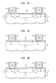
- FIG. 1 is a pictorial representation (through a cross-sectional view) showing the inventive CMOS device of the present invention.
- FIGS. 2A-2F are pictorial representations (through cross-sectional views) showing the basic processing steps of the present invention.
- FIGS. 3A-C are pictorial representations (through cross-sectional views) showing an embodiment wherein an epi Si layer is formed in the structure.
- FIG. 1 shows the basic CMOS device of the present invention.
- the structure shown in FIG. 1 comprises semiconductor substrate 10 having a plurality of patterned gate stack regions 12 formed thereon.
- Each patterned gate stack region includes at least gate dielectric 14 and gate material 16 .
- L-shaped nitride spacer 22 which includes vertical element 22 v and horizontal element 22 h , is formed on each exposed vertical sidewall on the patterned gate stack regions. Note that horizontal element 22 h of the L-shaped nitride spacer is formed on a portion of semiconductor substrate 10 , whereas the vertical element of the L-shaped nitride spacers is formed on the vertical sidewalls of the patterned gate regions.
- semiconductor substrate 10 includes deep source/drain regions 11 , shallow junction regions (not shown in the drawings), source/drain extension regions 15 and halo implant regions 17 .
- the CMOS device shown in FIG. 1 also includes silicide contacts 26 that are formed on exposed surfaces of the semiconductor substrate 10 that do not include horizontal element 22 h of L-shaped nitride spacer 22 .
- An important feature of the structure illustrated in FIG. 1 is the L-shaped nitride spacer which permits the formation of silicide contacts 26 that are self-aligned to the deep junction vertical edge present in the substrate. Such self-alignment of the silicide contacts with the deep junction edge as well as allowing the formation of shallow junctions is not achieved using any prior art process known to the inventors.
- FIG. 2A illustrates an initial structure that is employed in the present invention.
- the initial structure shown in FIG. 2A comprises semiconductor substrate 10 having a plurality of patterned gate stack regions 12 formed on portions of the semiconductor substrate.
- each patterned gate stack region includes at least gate dielectric 14 and gate material 16 formed atop the gate dielectric.
- semiconductor substrate 10 comprises any semiconducting material including, but not limited to: Si, Ge, SiGe, GaAs, InAs, InP and all other III/V semiconductor compounds.
- Semiconductor substrate 10 may also include a layered substrate comprising the same or different semiconducting material, e.g., Si/Si or Si/SiGe, as well as a silicon-on-insulator (SOI) substrate.
- the substrate may be of the n- or p-type depending on the desired device to be fabricated.
- semiconductor substrate 10 may contain active device regions, wiring regions, isolation regions or other like regions that are typically present in CMOS devices. For clarity, these regions are not shown in the drawings, but are nevertheless meant to be included within region 10 .
- semiconductor substrate 10 is comprised of Si or an SOI substrate. When an SOI substrate is employed, the CMOS device of the present invention is fabricated on the top Si-containing layer of the SOI substrate which is present above a buried oxide region.
- a layer of gate dielectric material 14 such as an oxide, nitride, oxynitride or any combination and multilayer thereof, is then formed on a surface of semiconductor substrate 10 utilizing a conventional process well known in the art.
- the layer of gate dielectric material may be formed by utilizing a conventional deposition process such as chemical vapor deposition (CVD), plasma-assisted CVD, evaporation or chemical solution deposition, or alternatively, the gate dielectric material may be formed by a thermal growing process such as oxidation, nitridation or oxynitridation.
- gate dielectric 14 has a thickness of from about 1 to about 20 nm after deposition, with a thickness of from about 1.5 to about 10 nm being more highly preferred.
- the gate dielectric material employed in the present invention may be a conventional dielectric material such as SiO 2 or Si 3 N 4 , or alternatively, high-k dielectrics such as oxides of Ta, Zr, Hf, Al or combinations thereof may be employed.
- gate dielectric 14 is comprised of an oxide such as SiO 2 , ZrO 2 , Ta 2 O 5 , HfO 2 or Al 2 O 3 .
- gate dielectric 14 After forming gate dielectric 14 on a surface of semiconductor substrate 10 , a gate stack including at least gate material 16 which may further contain an optional dielectric capping layer formed thereon is formed on gate dielectric 14 .
- gate material denotes a conductive material, a material that can be made conductive via a subsequent process such as ion implantation, or any combination thereof.
- Suitable gate materials include, but are not limited to: polysilicon, amorphous silicon, elemental metals that are conductive such as W, Pt, Pd, Ru, Rh and Ir, alloys of these elemental metals, silicides or nitrides of these elemental metals, and combinations thereof, e.g., a gate stack including a layer of polysilicon and a layer of conductive metal.
- a highly preferred gate material employed in the present invention is a gate material that is comprised of polysilicon or amorphous silicon.
- the gate material is formed on the surface of gate dielectric 14 utilizing conventional deposition processes well known in the art including, but not limited to: CVD, plasma-assisted CVD, evaporation, plating, or chemical solution deposition.
- a conventional silicide process may be used in forming the silicide layer.
- One such silicide process that can be used in the present invention includes the steps of: first forming an elemental metal such as W, Co, or Ti, annealing the layers so as to form a metal silicide layer therefrom, and removing any unreacted elemental metal utilizing a conventional wet etch process that has a high selectivity for removing elemental metal as compared to silicide.
- an optional diffusion barrier may be formed between each layer of the gate stack.
- the optional diffusion barrier which is formed utilizing conventional deposition processes such as those mentioned hereinabove, is comprised of a material such as SiN, TaN, TaSiN, WN, TiN and other like materials which can prevent diffusion of a conductive material therethrough.
- an optional dielectric capping layer may be present atop the gate material.
- the optional dielectric capping layer is comprised of an oxide, nitride or oxynitride and it is formed utilizing a conventional deposition process such as, for example, CVD or plasma-assisted CVD.
- a conventional thermal growing process such as, for example, oxidation, may be used in forming the optional dielectric capping layer.
- the gate stack and the gate dielectric are then patterned utilizing conventional processing steps well known in the art which are capable of forming patterned gate stack regions 12 shown in FIG. 2 A. Specifically, the patterning shown in FIG. 2A is formed by lithography and etching.
- the lithography step includes the following: applying a photoresist (not shown in the drawings) to the top surface of the gate stack, exposing the photoresist to a pattern of radiation and developing the pattern utilizing a conventional resist developer solution.
- Etching is performed utilizing a conventional dry etching process such as reactive-ion etching, plasma etching, ion beam etching, laser ablation or any combination thereof
- the etching step may remove portions of the gate stack and the underlying gate dielectric material that are not protected by the patterned photoresist in a single step, or alternatively, multiple etching steps may be performed wherein the exposed portions of the gate stack is first removed stopping on a surface of the gate dielectric, and thereafter the exposed portions of the gate dielectric are removed stopping on the surface of semiconductor substrate 10 .
- the patterned photoresist is removed utilizing a conventional stripping process well known in the art providing the structure shown, for example, in FIG. 2 A.
- the patterned gate stack regions are subjected to a conventional reoxidation process prior to proceeding to the next step of the present invention.
- spacers 18 which include a bilayer of thin nitride 20 followed by a thicker Si-containing film 24 such as silicon or silicon oxide are formed on exposed vertical sidewalls of each patterned gate stack region.
- Spacers 18 may be formed by first depositing a conformal nitride layer (via chemical vapor deposition or a similar conformal deposition process) on the structure shown in FIG. 2A, depositing a Si-containing film (via a conventional deposition process) on the nitride layer, and thereafter etching the Si-containing film (via an anisotropic spacer etch process). Note that nitride layer 20 remains on the structure after the Si-containing film has been etched.
- a preferred nitride layer employed in the present invention is Si 3 N 4 .
- the thickness of the conformal nitride layer formed at this point of the present invention is from about 3 to about 50 nm, with a thickness of from about 5 to about 35 nm being more highly preferred.
- that film has a thickness, after etching, of from about 20 to about 200 nm, with a thickness of from about 30 to about 150 nm being more highly preferred. Note that the above thickness are exemplary and that other thickness are also contemplated in the present invention.
- deep source/drain regions 11 are implanted into the surface of semiconductor substrate 10 utilizing a conventional ion implantation process well known in the art.
- the term “deep source/drain regions” is used herein to denote implant regions whose maximum implant depth is proportional to spacer 24 width, which from the top surface of the substrate is from about 30 to about 200 nm. It is noted that at this point of the present invention, it is also possible to implant dopants within the gate material.
- ion implantation conditions may be used in forming the deep source/drain regions within the substrate, but typically the ion implantation used in forming the deep source/drain regions is carried out at a dopant dosage of about 1E15 cm ⁇ 2 or greater using an implant energy of about 5 keV or greater. More preferably, the ion implantation used in forming the deep source/drain regions is carried out at a dopant dosage of from about 2E15 to about 2E16 cm ⁇ 2 using an implant energy of from about 7 to about 50 keV.
- the source/drain regions may be activated at this point of the present invention utilizing conventional activation annealing conditions well known to those skilled in the art. Although such an embodiment is possible, it is highly preferred to delay the activation of the S/D regions.
- the source/drain regions may be activated by annealing at a temperature of about 900° C. or greater, for a time period of from about 30 seconds or less. Other annealing conditions which are capable of activating the source/drain regions may also be employed in the present invention. It is again emphasized that although the source/drain regions may be activated at this point of the present invention, it is highly preferred to delay the activation of the source/drain regions until after shallow junction regions have been formed in the substrate.
- Si-containing film 24 of composite spacer 18 is removed from the structure utilizing a conventional etching process which is highly selective in removing the Si-containing film as compared to either the gate material or the nitride layer.
- the Si-containing film is removed from the structure utilizing a wet chemical etch process wherein a chemical etchant such as KOH is employed in selectively removing the Si-containing film.
- a chemical etchant such as KOH
- reactive-ion etching may be employed in selectively removing the Si-containing film from the composite spacer.
- thin nitride layer 20 remains on the patterned structure after removal of the Si-containing film.
- the resultant structure that is obtained after the aforementioned removal step of the present invention is shown, for example, in FIG. 2 C.
- FIG. 2D illustrates the structure after L-shaped nitride spacers 22 are formed. Specifically, following the removal of the thick Si spacers, portions of nitride layer 20 are removed so as to form L-shaped spacers 22 , each having vertical element 22 v and horizontal element 22 h . Specifically, the L-shaped nitride spacers are formed utilizing an etching process which is capable of selectively removing portions of the nitride layer. Note a photoresist may be placed over portions of the nitride layer that are not to be removed during this etching step.
- a preferred etching process which is employed in the present invention in removing portions of the nitride layer includes a wet chemical etch process wherein a chemical etchant such as H 3 PO 4 is employed. Using this etchant, the implanted regions of layer 20 are selectively etched leaving the unimplanted regions to form an L-shaped spacer.
- a chemical etchant such as H 3 PO 4
- the structure is subjected to a conventional activation annealing step which is capable of activating the shallow junctions, and optionally the deep source/drain regions.
- the activation annealing step is carried out utilizing the same conditions as mentioned hereinabove.
- shallow junction is used herein to denote an implant region whose maximum implant depth from the top surface of the substrate is from about 5 to about 50 nm.
- the implant energy is sufficient to penetrate under the L-shaped spacer forming extension regions near the gate.
- the ion implantation used in forming the shallow junction regions is carried out at a dopant dosage of about 2E15 cm ⁇ 2 or less using an implant energy of about 20 keV or less. More preferably, the ion implantation used in forming the shallow junction regions is carried out at a dopant dosage of from about 3E14 to about 1E15 cm ⁇ 2 using an implant energy of from about 0.5 to about 5 keV.
- halo implant regions 17 may be implanted into the surface of the semiconductor substrate providing the structure shown, for example, in FIG. 2 E. These implant regions are formed utilizing conventional ion implantation processes well known to those skilled in the art. Following the implantation of the source/drain extensions regions and the halo implant regions, each implant region is subjected to a conventional activation annealing process that is capable of activating both the source/drain extension regions and the halo implant regions.
- extension regions near the channel of the CMOS device are abrupt, i.e., less than about 10 nm/decade.
- the channel region is the portion of the semiconductor substrate which is beneath the patterned gate stack region.
- the halo profile in proximity to the extension junction is also abrupt, i.e., less than about 30 nm/decade.
- FIG. 2F shows the structure that is obtained after silicide contacts 26 are formed on portions of the semiconductor substrate 10 that are not protected by the horizontal element of the L-shaped nitride spacers.
- the silicide contacts are formed utilizing a conventional silicidation process which includes the steps of forming a layer of refractory metal, such as Ti, Ni or Co, or metal alloy on the exposed surfaces of the semiconductor substrate; annealing the layer of refractory metal under conditions that are capable of converting said refractory metal layer into a refractory metal silicide layer and, if needed, removing any non-reactant refractory metal from the structure that was not converted into a silicide layer.
- a conventional silicidation process which includes the steps of forming a layer of refractory metal, such as Ti, Ni or Co, or metal alloy on the exposed surfaces of the semiconductor substrate; annealing the layer of refractory metal under conditions that are capable of converting said refractory metal layer into a
- a typical annealing temperature used in forming the silicide contacts in the present invention is about 350° C. or greater, with an annealing temperature of from about 450° C. or greater being more highly preferred. Note that because of the L-shaped nitride spacers, the silicide contacts are self-aligned to the deep junction 11 vertical edge present in the underlying substrate.
- silicide regions are also formed atop each of the patterned gate stack regions. This embodiment of the present invention is not however depicted in the drawings of the present application.
- FIGS. 3A-3C show an embodiment of the present invention wherein raised/source drain regions are formed.
- the processing steps leading up to the structure shown in FIG. 2D are first performed.
- epi Si layer 28 is formed on exposed surfaces of semiconductor substrate 10 providing the structure shown in FIG. 3 A.
- the epi Si layer is formed utilizing conventional epitaxial growing processes well known in the art.
- the source/drain extension regions and halo implant regions are formed in the structure utilizing the above mentioned processes providing the structure shown, for example, in FIG. 3B, Silicide contacts 26 are then formed on the epi Si layer utilizing a conventional silicidation process, as was also mentioned hereinabove, providing the structure shown, for example, in FIG. 3 C.
Abstract
Description
Claims (11)
Priority Applications (2)
| Application Number | Priority Date | Filing Date | Title |
|---|---|---|---|
| US09/909,307 US6614079B2 (en) | 2001-07-19 | 2001-07-19 | All-in-one disposable/permanent spacer elevated source/drain, self-aligned silicide CMOS |
| US10/464,339 US6727135B2 (en) | 2001-07-19 | 2003-06-18 | All-in-one disposable/permanent spacer elevated source/drain, self-aligned silicide CMOS |
Applications Claiming Priority (1)
| Application Number | Priority Date | Filing Date | Title |
|---|---|---|---|
| US09/909,307 US6614079B2 (en) | 2001-07-19 | 2001-07-19 | All-in-one disposable/permanent spacer elevated source/drain, self-aligned silicide CMOS |
Related Child Applications (1)
| Application Number | Title | Priority Date | Filing Date |
|---|---|---|---|
| US10/464,339 Division US6727135B2 (en) | 2001-07-19 | 2003-06-18 | All-in-one disposable/permanent spacer elevated source/drain, self-aligned silicide CMOS |
Publications (2)
| Publication Number | Publication Date |
|---|---|
| US20030015762A1 US20030015762A1 (en) | 2003-01-23 |
| US6614079B2 true US6614079B2 (en) | 2003-09-02 |
Family
ID=25427000
Family Applications (2)
| Application Number | Title | Priority Date | Filing Date |
|---|---|---|---|
| US09/909,307 Expired - Lifetime US6614079B2 (en) | 2001-07-19 | 2001-07-19 | All-in-one disposable/permanent spacer elevated source/drain, self-aligned silicide CMOS |
| US10/464,339 Expired - Lifetime US6727135B2 (en) | 2001-07-19 | 2003-06-18 | All-in-one disposable/permanent spacer elevated source/drain, self-aligned silicide CMOS |
Family Applications After (1)
| Application Number | Title | Priority Date | Filing Date |
|---|---|---|---|
| US10/464,339 Expired - Lifetime US6727135B2 (en) | 2001-07-19 | 2003-06-18 | All-in-one disposable/permanent spacer elevated source/drain, self-aligned silicide CMOS |
Country Status (1)
| Country | Link |
|---|---|
| US (2) | US6614079B2 (en) |
Cited By (13)
| Publication number | Priority date | Publication date | Assignee | Title |
|---|---|---|---|---|
| US20030098489A1 (en) * | 2001-11-29 | 2003-05-29 | International Business Machines Corporation | High temperature processing compatible metal gate electrode for pFETS and methods for fabrication |
| US20030118948A1 (en) * | 2001-12-21 | 2003-06-26 | Rohit Grover | Method of etching semiconductor material to achieve structure suitable for optics |
| US20040140513A1 (en) * | 2002-08-22 | 2004-07-22 | Micron Technology, Inc. | Atomic layer deposition of CMOS gates with variable work functions |
| US20040157397A1 (en) * | 2003-02-10 | 2004-08-12 | Chartered Semiconductor Manufacturing Ltd. | Method of forming a pocket implant region after formation of composite insulator spacers |
| US20070122988A1 (en) * | 2005-11-29 | 2007-05-31 | International Business Machines Corporation | Methods of forming semiconductor devices using embedded l-shape spacers |
| US7256113B1 (en) * | 2001-12-14 | 2007-08-14 | Advanced Micro Devices, Inc. | System for forming a semiconductor device and method thereof |
| US7462903B1 (en) * | 2005-09-14 | 2008-12-09 | Spansion Llc | Methods for fabricating semiconductor devices and contacts to semiconductor devices |
| US20090039426A1 (en) * | 2007-08-10 | 2009-02-12 | International Business Machines Corporation | Extremely-thin silicon-on-insulator transistor with raised source/drain |
| US7709402B2 (en) | 2006-02-16 | 2010-05-04 | Micron Technology, Inc. | Conductive layers for hafnium silicon oxynitride films |
| TWI383501B (en) * | 2007-05-09 | 2013-01-21 | Sony Corp | Semiconductor device and semiconductor device manufacturing method |
| US8633110B2 (en) | 2005-07-20 | 2014-01-21 | Micron Technology, Inc. | Titanium nitride films |
| US8962434B2 (en) | 2012-07-10 | 2015-02-24 | International Business Machines Corporation | Field effect transistors with varying threshold voltages |
| US20150108586A1 (en) * | 2013-06-26 | 2015-04-23 | Globalfoundries Inc. | Transistor device with improved source/drain junction architecture and methods of making such a device |
Families Citing this family (15)
| Publication number | Priority date | Publication date | Assignee | Title |
|---|---|---|---|---|
| KR100763898B1 (en) * | 2003-08-02 | 2007-10-05 | 삼성전자주식회사 | Fabrication method of semiconductor device and semiconductor device fabricated using the same |
| US7125805B2 (en) * | 2004-05-05 | 2006-10-24 | Freescale Semiconductor, Inc. | Method of semiconductor fabrication incorporating disposable spacer into elevated source/drain processing |
| US7274073B2 (en) | 2004-10-08 | 2007-09-25 | International Business Machines Corporation | Integrated circuit with bulk and SOI devices connected with an epitaxial region |
| US20060094194A1 (en) * | 2004-11-04 | 2006-05-04 | Taiwan Semiconductor Manufacturing Company, Ltd. | Advanced disposable spacer process by low-temperature high-stress nitride film for sub-90NM CMOS technology |
| KR100618908B1 (en) * | 2005-08-12 | 2006-09-05 | 삼성전자주식회사 | Semiconductor device for improving resistance of gate and method of manufacturing the same |
| US7488660B2 (en) * | 2006-02-21 | 2009-02-10 | International Business Machines Corporation | Extended raised source/drain structure for enhanced contact area and method for forming extended raised source/drain structure |
| US7618867B2 (en) * | 2006-07-26 | 2009-11-17 | Infineon Technologies Ag | Method of forming a doped portion of a semiconductor and method of forming a transistor |
| US7598572B2 (en) * | 2006-10-25 | 2009-10-06 | International Business Machines Corporation | Silicided polysilicon spacer for enhanced contact area |
| US7732298B2 (en) * | 2007-01-31 | 2010-06-08 | Taiwan Semiconductor Manufacturing Company, Ltd. | Metal salicide formation having nitride liner to reduce silicide stringer and encroachment |
| DE102007025326B4 (en) * | 2007-05-31 | 2011-01-20 | Advanced Micro Devices, Inc., Sunnyvale | A method of forming a semiconductor structure comprising implanting ions into a material layer to be etched |
| US7799650B2 (en) | 2007-08-08 | 2010-09-21 | Freescale Semiconductor, Inc. | Method for making a transistor with a stressor |
| US20100038705A1 (en) * | 2008-08-12 | 2010-02-18 | International Business Machines Corporation | Field effect device with gate electrode edge enhanced gate dielectric and method for fabrication |
| US8652963B2 (en) * | 2011-09-20 | 2014-02-18 | GlobalFoundries, Inc. | MOSFET integrated circuit with uniformly thin silicide layer and methods for its manufacture |
| US10003014B2 (en) * | 2014-06-20 | 2018-06-19 | International Business Machines Corporation | Method of forming an on-pitch self-aligned hard mask for contact to a tunnel junction using ion beam etching |
| DE102018124675A1 (en) | 2017-11-30 | 2019-06-06 | Taiwan Semiconductor Manufacturing Co., Ltd. | Annealing of film at different temperatures and structures formed thereby |
Citations (3)
| Publication number | Priority date | Publication date | Assignee | Title |
|---|---|---|---|---|
| US5716862A (en) * | 1993-05-26 | 1998-02-10 | Micron Technology, Inc. | High performance PMOSFET using split-polysilicon CMOS process incorporating advanced stacked capacitior cells for fabricating multi-megabit DRAMS |
| US6025267A (en) * | 1998-07-15 | 2000-02-15 | Chartered Semiconductor Manufacturing, Ltd. | Silicon nitride--TEOS oxide, salicide blocking layer for deep sub-micron devices |
| US6165826A (en) * | 1994-12-23 | 2000-12-26 | Intel Corporation | Transistor with low resistance tip and method of fabrication in a CMOS process |
Family Cites Families (9)
| Publication number | Priority date | Publication date | Assignee | Title |
|---|---|---|---|---|
| US4843023A (en) * | 1985-09-25 | 1989-06-27 | Hewlett-Packard Company | Process for forming lightly-doped-drain (LDD) without extra masking steps |
| US4818714A (en) * | 1987-12-02 | 1989-04-04 | Advanced Micro Devices, Inc. | Method of making a high performance MOS device having LDD regions with graded junctions |
| JPH1187703A (en) * | 1997-09-10 | 1999-03-30 | Toshiba Corp | Manufacture of semiconductor device |
| US6087234A (en) * | 1997-12-19 | 2000-07-11 | Texas Instruments - Acer Incorporated | Method of forming a self-aligned silicide MOSFET with an extended ultra-shallow S/D junction |
| US6177323B1 (en) * | 1998-03-02 | 2001-01-23 | Texas Instruments - Acer Incorporated | Method to form MOSFET with an elevated source/drain for PMOSFET |
| US6065826A (en) * | 1998-10-06 | 2000-05-23 | Hewlett-Packard Company | Modular print cartridge receptacle for use in inkjet printing systems |
| US6228730B1 (en) * | 1999-04-28 | 2001-05-08 | United Microelectronics Corp. | Method of fabricating field effect transistor |
| US6087235A (en) * | 1999-10-14 | 2000-07-11 | Advanced Micro Devices, Inc. | Method for effective fabrication of a field effect transistor with elevated drain and source contact structures |
| US6277683B1 (en) * | 2000-02-28 | 2001-08-21 | Chartered Semiconductor Manufacturing Ltd. | Method of forming a sidewall spacer and a salicide blocking shape, using only one silicon nitride layer |
-
2001
- 2001-07-19 US US09/909,307 patent/US6614079B2/en not_active Expired - Lifetime
-
2003
- 2003-06-18 US US10/464,339 patent/US6727135B2/en not_active Expired - Lifetime
Patent Citations (3)
| Publication number | Priority date | Publication date | Assignee | Title |
|---|---|---|---|---|
| US5716862A (en) * | 1993-05-26 | 1998-02-10 | Micron Technology, Inc. | High performance PMOSFET using split-polysilicon CMOS process incorporating advanced stacked capacitior cells for fabricating multi-megabit DRAMS |
| US6165826A (en) * | 1994-12-23 | 2000-12-26 | Intel Corporation | Transistor with low resistance tip and method of fabrication in a CMOS process |
| US6025267A (en) * | 1998-07-15 | 2000-02-15 | Chartered Semiconductor Manufacturing, Ltd. | Silicon nitride--TEOS oxide, salicide blocking layer for deep sub-micron devices |
Cited By (25)
| Publication number | Priority date | Publication date | Assignee | Title |
|---|---|---|---|---|
| US20030098489A1 (en) * | 2001-11-29 | 2003-05-29 | International Business Machines Corporation | High temperature processing compatible metal gate electrode for pFETS and methods for fabrication |
| US7863083B2 (en) | 2001-11-29 | 2011-01-04 | International Business Machines Corporation | High temperature processing compatible metal gate electrode for pFETS and methods for fabrication |
| US20080311745A1 (en) * | 2001-11-29 | 2008-12-18 | International Business Machines Corporation | High Temperature Processing Compatible Metal Gate Electrode For pFETS and Methods For Fabrication |
| US7256113B1 (en) * | 2001-12-14 | 2007-08-14 | Advanced Micro Devices, Inc. | System for forming a semiconductor device and method thereof |
| US20030118948A1 (en) * | 2001-12-21 | 2003-06-26 | Rohit Grover | Method of etching semiconductor material to achieve structure suitable for optics |
| US7351628B2 (en) | 2002-08-22 | 2008-04-01 | Micron Technology, Inc. | Atomic layer deposition of CMOS gates with variable work functions |
| US20050032342A1 (en) * | 2002-08-22 | 2005-02-10 | Micron Technology, Inc. | Atomic layer deposition of CMOS gates with variable work functions |
| US20040140513A1 (en) * | 2002-08-22 | 2004-07-22 | Micron Technology, Inc. | Atomic layer deposition of CMOS gates with variable work functions |
| US6924180B2 (en) * | 2003-02-10 | 2005-08-02 | Chartered Semiconductor Manufacturing Ltd. | Method of forming a pocket implant region after formation of composite insulator spacers |
| US20040157397A1 (en) * | 2003-02-10 | 2004-08-12 | Chartered Semiconductor Manufacturing Ltd. | Method of forming a pocket implant region after formation of composite insulator spacers |
| US8633110B2 (en) | 2005-07-20 | 2014-01-21 | Micron Technology, Inc. | Titanium nitride films |
| US7462903B1 (en) * | 2005-09-14 | 2008-12-09 | Spansion Llc | Methods for fabricating semiconductor devices and contacts to semiconductor devices |
| US20070122988A1 (en) * | 2005-11-29 | 2007-05-31 | International Business Machines Corporation | Methods of forming semiconductor devices using embedded l-shape spacers |
| US7759206B2 (en) | 2005-11-29 | 2010-07-20 | International Business Machines Corporation | Methods of forming semiconductor devices using embedded L-shape spacers |
| US8067794B2 (en) | 2006-02-16 | 2011-11-29 | Micron Technology, Inc. | Conductive layers for hafnium silicon oxynitride films |
| US8785312B2 (en) | 2006-02-16 | 2014-07-22 | Micron Technology, Inc. | Conductive layers for hafnium silicon oxynitride |
| US7709402B2 (en) | 2006-02-16 | 2010-05-04 | Micron Technology, Inc. | Conductive layers for hafnium silicon oxynitride films |
| TWI383501B (en) * | 2007-05-09 | 2013-01-21 | Sony Corp | Semiconductor device and semiconductor device manufacturing method |
| US7871869B2 (en) | 2007-08-10 | 2011-01-18 | International Business Machines Corporation | Extremely-thin silicon-on-insulator transistor with raised source/drain |
| US7652332B2 (en) | 2007-08-10 | 2010-01-26 | International Business Machines Corporation | Extremely-thin silicon-on-insulator transistor with raised source/drain |
| US20090039426A1 (en) * | 2007-08-10 | 2009-02-12 | International Business Machines Corporation | Extremely-thin silicon-on-insulator transistor with raised source/drain |
| US8962434B2 (en) | 2012-07-10 | 2015-02-24 | International Business Machines Corporation | Field effect transistors with varying threshold voltages |
| US9673196B2 (en) | 2012-07-10 | 2017-06-06 | GlobalFoundries, Inc. | Field effect transistors with varying threshold voltages |
| US20150108586A1 (en) * | 2013-06-26 | 2015-04-23 | Globalfoundries Inc. | Transistor device with improved source/drain junction architecture and methods of making such a device |
| US9178053B2 (en) * | 2013-06-26 | 2015-11-03 | Globalfoundries Inc. | Transistor device with improved source/drain junction architecture and methods of making such a device |
Also Published As
| Publication number | Publication date |
|---|---|
| US20030015762A1 (en) | 2003-01-23 |
| US20030209765A1 (en) | 2003-11-13 |
| US6727135B2 (en) | 2004-04-27 |
Similar Documents
| Publication | Publication Date | Title |
|---|---|---|
| US6614079B2 (en) | All-in-one disposable/permanent spacer elevated source/drain, self-aligned silicide CMOS | |
| US10374068B2 (en) | Tunnel field effect transistors | |
| US6432754B1 (en) | Double SOI device with recess etch and epitaxy | |
| US6720630B2 (en) | Structure and method for MOSFET with metallic gate electrode | |
| US7459752B2 (en) | Ultra thin body fully-depleted SOI MOSFETs | |
| US6512266B1 (en) | Method of fabricating SiO2 spacers and annealing caps | |
| US6743686B2 (en) | Sacrificial polysilicon sidewall process and rapid thermal spike annealing for advance CMOS fabrication | |
| US7314794B2 (en) | Low-cost high-performance planar back-gate CMOS | |
| US6656824B1 (en) | Low resistance T-gate MOSFET device using a damascene gate process and an innovative oxide removal etch | |
| US6432763B1 (en) | Field effect transistor having doped gate with prevention of contamination from the gate during implantation | |
| US7074684B2 (en) | Elevated source drain disposable spacer CMOS | |
| US20040135212A1 (en) | Damascene method for improved mos transistor | |
| US20070275532A1 (en) | Optimized deep source/drain junctions with thin poly gate in a field effect transistor | |
| EP1205980A1 (en) | A method for forming a field effect transistor in a semiconductor substrate | |
| US6437406B1 (en) | Super-halo formation in FETs | |
| US8658530B2 (en) | Method of fabricating an epitaxial Ni silicide film | |
| JP2009509359A (en) | Multiple low and high K gate oxides on a single gate for reduced mirror capacitance and improved drive current | |
| US20100117163A1 (en) | Semiconductor device and method of fabricating the same | |
| US6469350B1 (en) | Active well schemes for SOI technology | |
| JP2003188373A (en) | Semiconductor device and method of manufacturing the same | |
| US6635517B2 (en) | Use of disposable spacer to introduce gettering in SOI layer | |
| US6365468B1 (en) | Method for forming doped p-type gate with anti-reflection layer | |
| US7851297B2 (en) | Dual workfunction semiconductor device | |
| JP2004253707A (en) | Semiconductor device, and manufacturing method thereof |
Legal Events
| Date | Code | Title | Description |
|---|---|---|---|
| AS | Assignment |
Owner name: INTERNATIONAL BUSINESS MACHINES CORPORATION, NEW Y Free format text: ASSIGNMENT OF ASSIGNORS INTEREST;ASSIGNORS:LEE, KAM LEUNG;ROY, RONNEN ANDREW;REEL/FRAME:012026/0527 Effective date: 20010716 |
|
| STCF | Information on status: patent grant |
Free format text: PATENTED CASE |
|
| FEPP | Fee payment procedure |
Free format text: PAYOR NUMBER ASSIGNED (ORIGINAL EVENT CODE: ASPN); ENTITY STATUS OF PATENT OWNER: LARGE ENTITY |
|
| CC | Certificate of correction | ||
| FPAY | Fee payment |
Year of fee payment: 4 |
|
| FPAY | Fee payment |
Year of fee payment: 8 |
|
| FPAY | Fee payment |
Year of fee payment: 12 |
|
| AS | Assignment |
Owner name: GLOBALFOUNDRIES U.S. 2 LLC, NEW YORK Free format text: ASSIGNMENT OF ASSIGNORS INTEREST;ASSIGNOR:INTERNATIONAL BUSINESS MACHINES CORPORATION;REEL/FRAME:036550/0001 Effective date: 20150629 |
|
| AS | Assignment |
Owner name: GLOBALFOUNDRIES INC., CAYMAN ISLANDS Free format text: ASSIGNMENT OF ASSIGNORS INTEREST;ASSIGNORS:GLOBALFOUNDRIES U.S. 2 LLC;GLOBALFOUNDRIES U.S. INC.;REEL/FRAME:036779/0001 Effective date: 20150910 |
|
| AS | Assignment |
Owner name: WILMINGTON TRUST, NATIONAL ASSOCIATION, DELAWARE Free format text: SECURITY AGREEMENT;ASSIGNOR:GLOBALFOUNDRIES INC.;REEL/FRAME:049490/0001 Effective date: 20181127 |
|
| AS | Assignment |
Owner name: GLOBALFOUNDRIES U.S. INC., CALIFORNIA Free format text: ASSIGNMENT OF ASSIGNORS INTEREST;ASSIGNOR:GLOBALFOUNDRIES INC.;REEL/FRAME:054633/0001 Effective date: 20201022 |
|
| AS | Assignment |
Owner name: GLOBALFOUNDRIES INC., CAYMAN ISLANDS Free format text: RELEASE BY SECURED PARTY;ASSIGNOR:WILMINGTON TRUST, NATIONAL ASSOCIATION;REEL/FRAME:054636/0001 Effective date: 20201117 |
|
| AS | Assignment |
Owner name: GLOBALFOUNDRIES U.S. INC., NEW YORK Free format text: RELEASE BY SECURED PARTY;ASSIGNOR:WILMINGTON TRUST, NATIONAL ASSOCIATION;REEL/FRAME:056987/0001 Effective date: 20201117 |