US6528362B1 - Metal gate with CVD amorphous silicon layer for CMOS devices and method of making with a replacement gate process - Google Patents
Metal gate with CVD amorphous silicon layer for CMOS devices and method of making with a replacement gate process Download PDFInfo
- Publication number
- US6528362B1 US6528362B1 US09/691,181 US69118100A US6528362B1 US 6528362 B1 US6528362 B1 US 6528362B1 US 69118100 A US69118100 A US 69118100A US 6528362 B1 US6528362 B1 US 6528362B1
- Authority
- US
- United States
- Prior art keywords
- gate
- amorphous silicon
- metal
- recess
- silicon layer
- Prior art date
- Legal status (The legal status is an assumption and is not a legal conclusion. Google has not performed a legal analysis and makes no representation as to the accuracy of the status listed.)
- Expired - Lifetime, expires
Links
- 229910052751 metal Inorganic materials 0.000 title claims abstract description 45
- 239000002184 metal Substances 0.000 title claims abstract description 45
- 229910021417 amorphous silicon Inorganic materials 0.000 title claims abstract description 40
- 238000000034 method Methods 0.000 title claims abstract description 25
- 238000004519 manufacturing process Methods 0.000 title 1
- 239000004065 semiconductor Substances 0.000 claims abstract description 27
- 239000000758 substrate Substances 0.000 claims abstract description 20
- 238000000151 deposition Methods 0.000 claims description 20
- 230000008021 deposition Effects 0.000 claims description 14
- 238000005229 chemical vapour deposition Methods 0.000 claims description 9
- 238000000623 plasma-assisted chemical vapour deposition Methods 0.000 claims description 6
- 125000006850 spacer group Chemical group 0.000 claims description 5
- 239000002243 precursor Substances 0.000 claims description 4
- 238000011065 in-situ storage Methods 0.000 claims description 2
- 229910052750 molybdenum Inorganic materials 0.000 claims description 2
- 229910052759 nickel Inorganic materials 0.000 claims description 2
- 229910052719 titanium Inorganic materials 0.000 claims description 2
- 229910052721 tungsten Inorganic materials 0.000 claims description 2
- 229910021420 polycrystalline silicon Inorganic materials 0.000 abstract description 31
- 229920005591 polysilicon Polymers 0.000 abstract description 31
- XUIMIQQOPSSXEZ-UHFFFAOYSA-N Silicon Chemical compound [Si] XUIMIQQOPSSXEZ-UHFFFAOYSA-N 0.000 abstract description 13
- 229910052710 silicon Inorganic materials 0.000 abstract description 13
- 239000010703 silicon Substances 0.000 abstract description 13
- 239000000126 substance Substances 0.000 abstract description 5
- 239000000463 material Substances 0.000 description 10
- 230000015572 biosynthetic process Effects 0.000 description 5
- VYPSYNLAJGMNEJ-UHFFFAOYSA-N Silicium dioxide Chemical compound O=[Si]=O VYPSYNLAJGMNEJ-UHFFFAOYSA-N 0.000 description 3
- 239000007769 metal material Substances 0.000 description 3
- PXHVJJICTQNCMI-UHFFFAOYSA-N Nickel Chemical compound [Ni] PXHVJJICTQNCMI-UHFFFAOYSA-N 0.000 description 2
- XYFCBTPGUUZFHI-UHFFFAOYSA-N Phosphine Chemical compound P XYFCBTPGUUZFHI-UHFFFAOYSA-N 0.000 description 2
- BLRPTPMANUNPDV-UHFFFAOYSA-N Silane Chemical compound [SiH4] BLRPTPMANUNPDV-UHFFFAOYSA-N 0.000 description 2
- MCMNRKCIXSYSNV-UHFFFAOYSA-N Zirconium dioxide Chemical compound O=[Zr]=O MCMNRKCIXSYSNV-UHFFFAOYSA-N 0.000 description 2
- 239000006117 anti-reflective coating Substances 0.000 description 2
- 239000003989 dielectric material Substances 0.000 description 2
- 238000005468 ion implantation Methods 0.000 description 2
- 229910000077 silane Inorganic materials 0.000 description 2
- ZAMOUSCENKQFHK-UHFFFAOYSA-N Chlorine atom Chemical compound [Cl] ZAMOUSCENKQFHK-UHFFFAOYSA-N 0.000 description 1
- ZOKXTWBITQBERF-UHFFFAOYSA-N Molybdenum Chemical compound [Mo] ZOKXTWBITQBERF-UHFFFAOYSA-N 0.000 description 1
- 229910052581 Si3N4 Inorganic materials 0.000 description 1
- 229910004160 TaO2 Inorganic materials 0.000 description 1
- RTAQQCXQSZGOHL-UHFFFAOYSA-N Titanium Chemical compound [Ti] RTAQQCXQSZGOHL-UHFFFAOYSA-N 0.000 description 1
- 239000000654 additive Substances 0.000 description 1
- 230000000903 blocking effect Effects 0.000 description 1
- 239000000969 carrier Substances 0.000 description 1
- 229910052801 chlorine Inorganic materials 0.000 description 1
- 239000000460 chlorine Substances 0.000 description 1
- 238000007796 conventional method Methods 0.000 description 1
- 230000008878 coupling Effects 0.000 description 1
- 238000010168 coupling process Methods 0.000 description 1
- 238000005859 coupling reaction Methods 0.000 description 1
- 238000005137 deposition process Methods 0.000 description 1
- NQKXFODBPINZFK-UHFFFAOYSA-N dioxotantalum Chemical compound O=[Ta]=O NQKXFODBPINZFK-UHFFFAOYSA-N 0.000 description 1
- 239000002019 doping agent Substances 0.000 description 1
- 230000005684 electric field Effects 0.000 description 1
- 238000005516 engineering process Methods 0.000 description 1
- CJNBYAVZURUTKZ-UHFFFAOYSA-N hafnium(IV) oxide Inorganic materials O=[Hf]=O CJNBYAVZURUTKZ-UHFFFAOYSA-N 0.000 description 1
- 238000002513 implantation Methods 0.000 description 1
- 150000002500 ions Chemical class 0.000 description 1
- 229910044991 metal oxide Inorganic materials 0.000 description 1
- 150000004706 metal oxides Chemical class 0.000 description 1
- 150000002739 metals Chemical class 0.000 description 1
- 239000011733 molybdenum Substances 0.000 description 1
- 229910021334 nickel silicide Inorganic materials 0.000 description 1
- RUFLMLWJRZAWLJ-UHFFFAOYSA-N nickel silicide Chemical compound [Ni]=[Si]=[Ni] RUFLMLWJRZAWLJ-UHFFFAOYSA-N 0.000 description 1
- 230000003647 oxidation Effects 0.000 description 1
- 238000007254 oxidation reaction Methods 0.000 description 1
- 238000000059 patterning Methods 0.000 description 1
- 229910000073 phosphorus hydride Inorganic materials 0.000 description 1
- 229910021332 silicide Inorganic materials 0.000 description 1
- FVBUAEGBCNSCDD-UHFFFAOYSA-N silicide(4-) Chemical compound [Si-4] FVBUAEGBCNSCDD-UHFFFAOYSA-N 0.000 description 1
- 235000012239 silicon dioxide Nutrition 0.000 description 1
- 239000000377 silicon dioxide Substances 0.000 description 1
- HQVNEWCFYHHQES-UHFFFAOYSA-N silicon nitride Chemical compound N12[Si]34N5[Si]62N3[Si]51N64 HQVNEWCFYHHQES-UHFFFAOYSA-N 0.000 description 1
- 229910052814 silicon oxide Inorganic materials 0.000 description 1
- XUIMIQQOPSSXEZ-IGMARMGPSA-N silicon-28 atom Chemical compound [28Si] XUIMIQQOPSSXEZ-IGMARMGPSA-N 0.000 description 1
- 239000010936 titanium Substances 0.000 description 1
- WFKWXMTUELFFGS-UHFFFAOYSA-N tungsten Chemical compound [W] WFKWXMTUELFFGS-UHFFFAOYSA-N 0.000 description 1
- 239000010937 tungsten Substances 0.000 description 1
- 230000005641 tunneling Effects 0.000 description 1
Images

Classifications
-
- H—ELECTRICITY
- H01—ELECTRIC ELEMENTS
- H01L—SEMICONDUCTOR DEVICES NOT COVERED BY CLASS H10
- H01L21/00—Processes or apparatus adapted for the manufacture or treatment of semiconductor or solid state devices or of parts thereof
- H01L21/02—Manufacture or treatment of semiconductor devices or of parts thereof
- H01L21/04—Manufacture or treatment of semiconductor devices or of parts thereof the devices having at least one potential-jump barrier or surface barrier, e.g. PN junction, depletion layer or carrier concentration layer
- H01L21/18—Manufacture or treatment of semiconductor devices or of parts thereof the devices having at least one potential-jump barrier or surface barrier, e.g. PN junction, depletion layer or carrier concentration layer the devices having semiconductor bodies comprising elements of Group IV of the Periodic System or AIIIBV compounds with or without impurities, e.g. doping materials
- H01L21/28—Manufacture of electrodes on semiconductor bodies using processes or apparatus not provided for in groups H01L21/20 - H01L21/268
- H01L21/28008—Making conductor-insulator-semiconductor electrodes
- H01L21/28017—Making conductor-insulator-semiconductor electrodes the insulator being formed after the semiconductor body, the semiconductor being silicon
- H01L21/28158—Making the insulator
- H01L21/28167—Making the insulator on single crystalline silicon, e.g. using a liquid, i.e. chemical oxidation
- H01L21/28194—Making the insulator on single crystalline silicon, e.g. using a liquid, i.e. chemical oxidation by deposition, e.g. evaporation, ALD, CVD, sputtering, laser deposition
-
- H—ELECTRICITY
- H01—ELECTRIC ELEMENTS
- H01L—SEMICONDUCTOR DEVICES NOT COVERED BY CLASS H10
- H01L21/00—Processes or apparatus adapted for the manufacture or treatment of semiconductor or solid state devices or of parts thereof
- H01L21/02—Manufacture or treatment of semiconductor devices or of parts thereof
- H01L21/04—Manufacture or treatment of semiconductor devices or of parts thereof the devices having at least one potential-jump barrier or surface barrier, e.g. PN junction, depletion layer or carrier concentration layer
- H01L21/18—Manufacture or treatment of semiconductor devices or of parts thereof the devices having at least one potential-jump barrier or surface barrier, e.g. PN junction, depletion layer or carrier concentration layer the devices having semiconductor bodies comprising elements of Group IV of the Periodic System or AIIIBV compounds with or without impurities, e.g. doping materials
- H01L21/28—Manufacture of electrodes on semiconductor bodies using processes or apparatus not provided for in groups H01L21/20 - H01L21/268
- H01L21/28008—Making conductor-insulator-semiconductor electrodes
- H01L21/28017—Making conductor-insulator-semiconductor electrodes the insulator being formed after the semiconductor body, the semiconductor being silicon
- H01L21/28026—Making conductor-insulator-semiconductor electrodes the insulator being formed after the semiconductor body, the semiconductor being silicon characterised by the conductor
- H01L21/28035—Making conductor-insulator-semiconductor electrodes the insulator being formed after the semiconductor body, the semiconductor being silicon characterised by the conductor the final conductor layer next to the insulator being silicon, e.g. polysilicon, with or without impurities
- H01L21/28044—Making conductor-insulator-semiconductor electrodes the insulator being formed after the semiconductor body, the semiconductor being silicon characterised by the conductor the final conductor layer next to the insulator being silicon, e.g. polysilicon, with or without impurities the conductor comprising at least another non-silicon conductive layer
- H01L21/28061—Making conductor-insulator-semiconductor electrodes the insulator being formed after the semiconductor body, the semiconductor being silicon characterised by the conductor the final conductor layer next to the insulator being silicon, e.g. polysilicon, with or without impurities the conductor comprising at least another non-silicon conductive layer the conductor comprising a metal or metal silicide formed by deposition, e.g. sputter deposition, i.e. without a silicidation reaction
-
- H—ELECTRICITY
- H01—ELECTRIC ELEMENTS
- H01L—SEMICONDUCTOR DEVICES NOT COVERED BY CLASS H10
- H01L29/00—Semiconductor devices adapted for rectifying, amplifying, oscillating or switching, or capacitors or resistors with at least one potential-jump barrier or surface barrier, e.g. PN junction depletion layer or carrier concentration layer; Details of semiconductor bodies or of electrodes thereof ; Multistep manufacturing processes therefor
- H01L29/40—Electrodes ; Multistep manufacturing processes therefor
- H01L29/43—Electrodes ; Multistep manufacturing processes therefor characterised by the materials of which they are formed
- H01L29/49—Metal-insulator-semiconductor electrodes, e.g. gates of MOSFET
- H01L29/4916—Metal-insulator-semiconductor electrodes, e.g. gates of MOSFET the conductor material next to the insulator being a silicon layer, e.g. polysilicon doped with boron, phosphorus or nitrogen
- H01L29/4925—Metal-insulator-semiconductor electrodes, e.g. gates of MOSFET the conductor material next to the insulator being a silicon layer, e.g. polysilicon doped with boron, phosphorus or nitrogen with a multiple layer structure, e.g. several silicon layers with different crystal structure or grain arrangement
-
- H—ELECTRICITY
- H01—ELECTRIC ELEMENTS
- H01L—SEMICONDUCTOR DEVICES NOT COVERED BY CLASS H10
- H01L29/00—Semiconductor devices adapted for rectifying, amplifying, oscillating or switching, or capacitors or resistors with at least one potential-jump barrier or surface barrier, e.g. PN junction depletion layer or carrier concentration layer; Details of semiconductor bodies or of electrodes thereof ; Multistep manufacturing processes therefor
- H01L29/40—Electrodes ; Multistep manufacturing processes therefor
- H01L29/43—Electrodes ; Multistep manufacturing processes therefor characterised by the materials of which they are formed
- H01L29/49—Metal-insulator-semiconductor electrodes, e.g. gates of MOSFET
- H01L29/51—Insulating materials associated therewith
- H01L29/517—Insulating materials associated therewith the insulating material comprising a metallic compound, e.g. metal oxide, metal silicate
-
- H—ELECTRICITY
- H01—ELECTRIC ELEMENTS
- H01L—SEMICONDUCTOR DEVICES NOT COVERED BY CLASS H10
- H01L29/00—Semiconductor devices adapted for rectifying, amplifying, oscillating or switching, or capacitors or resistors with at least one potential-jump barrier or surface barrier, e.g. PN junction depletion layer or carrier concentration layer; Details of semiconductor bodies or of electrodes thereof ; Multistep manufacturing processes therefor
- H01L29/66—Types of semiconductor device ; Multistep manufacturing processes therefor
- H01L29/66007—Multistep manufacturing processes
- H01L29/66075—Multistep manufacturing processes of devices having semiconductor bodies comprising group 14 or group 13/15 materials
- H01L29/66227—Multistep manufacturing processes of devices having semiconductor bodies comprising group 14 or group 13/15 materials the devices being controllable only by the electric current supplied or the electric potential applied, to an electrode which does not carry the current to be rectified, amplified or switched, e.g. three-terminal devices
- H01L29/66409—Unipolar field-effect transistors
- H01L29/66477—Unipolar field-effect transistors with an insulated gate, i.e. MISFET
- H01L29/66545—Unipolar field-effect transistors with an insulated gate, i.e. MISFET using a dummy, i.e. replacement gate in a process wherein at least a part of the final gate is self aligned to the dummy gate
Definitions
- the present invention contains subject matter similar to that disclosed in U.S. patent application Ser. No. 09/691,224, filed on Oct. 19, 2000, now U.S. Pat. No. 6,392,280; issued May. 21, 2002; U.S. patent application Ser. No. 09/691,259, filed on Oct. 19, 2000, now U.S. Pat. No. 6,440,868; issued Aug. 27, 2002; U.S. patent application Ser. No. 09/691,179, filed on Oct. 19, 2000, now abandoned; and U.S. patent application Ser. No. 09/691,188, filed on Oct. 19, 2000, now U.S. Pat. No. 6,436,840, issued Aug. 20, 2002.
- the present invention relates to the field of semiconductor processing, and more particularly, to the formation of metallic gate electrodes using the replacement gate process technique.
- MOS transistors In the integrated circuit (IC) industry, metal-oxide-semiconductor (MOS) transistors have typically been formed utilizing polysilicon gate electrodes.
- Polysilicon material has been preferred for use as an MOS gate electrode due to its thermal resistive properties (i.e., polysilicon can better withstand subsequent high temperature processing).
- Polysilicon's robustness during high temperature processing allows polysilicon to be annealed at high temperatures along with source and drain regions.
- polysilicon's ability to block the ion implantation of doped atoms into a channel region is advantageous. Due to the ion implantation blocking potential of polysilicon, polysilicon allows for the easy formation of self-aligned source and drain structures after gate patterning is completed.
- polysilicon gate electrodes have certain disadvantages.
- polysilicon gate electrodes are formed from semiconductor materials that suffer from higher resistivities than most metal materials. Therefore, polysilicon gate electrodes may operate at much slower speeds than gates made of metallic materials. To partially compensate for this higher resistance, polysilicon materials often require extensive and expensive silicide processing in order to increase their speed of operation to acceptable levels.
- metal gates can not withstand the higher temperatures and oxidation ambients which can be withstood by conventional polysilicon gate electrodes.
- a replacement damascene metal gate process has been created.
- a damascene gate process uses a disposable gate, which is formed with a source, drain, spacer, etch stops and anti-reflective coatings as in conventional processing. The disposable gate and dielectrics are etched away, exposing an original gate oxide. The disposable polysilicon gate is then replaced by a metal gate to achieve the lower resistivity provided by the metal material.
- a design consideration in semiconductor technology is that of the work function, which is the amount of energy required to excite electrons across a threshold.
- Polysilicon gates on silicon substrates provide a work function that allows the gates to be adequately controlled.
- the use of metal, however, as the gate material on a silicon substrate undesirably changes the work function in comparison to polysilicon gates. This reduces the controllability of the gate.
- This and other needs are met by the embodiments of the present invention which provide a semiconductor structure comprising a substrate, active regions in the substrate, and a gate structure on the substrate.
- This gate structure includes a high dielectric constant (high k) gate dielectric on the substrate, a chemical vapor deposited (CVD) layer of amorphous silicon on the high k gate dielectric, and a metal on the CVD amorphous silicon layer.
- high k high dielectric constant
- CVD chemical vapor deposited
- the advantages of a metal gate including that of lower resistivity, is achieved without compromising the work function of the gate structure.
- the CVD amorphous silicon layer causes the work function of the metal gate to appear like a standard gate.
- embodiments of the present invention provide a method of forming a semiconductor structure, comprising the steps of forming a precursor having a substrate with active regions separated by a channel, and a temporary gate over the channel and between dielectric structures.
- the temporary gate is removed to form a recess with a bottom and sidewalls between the dielectric structures.
- Amorphous silicon is deposited in the recess by chemical vapor deposition.
- the metal is then deposited in the recess on the amorphous silicon.
- the formation of a semiconductor structure in accordance with the present invention is advantageous in that high-temperature processes may be performed prior to the deposition of the metal gate. Also, the formation of source and drain electrodes self-aligned to the subsequently formed metal gate is possible. The formation of the metal gate in this replacement gate process, however, allows the metal gate to be formed after the implantation of the dopant atoms. By depositing amorphous silicon in the recess by chemical vapor deposition prior to the depositing of the metal in the recess on the amorphous silicon, the work function will be same as if the gate were made of polysilicon instead of metal. This provides increased control of the gate and avoids leakage.
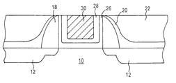
- FIG. 1 is a schematic depiction of a cross-section of a semiconductor structure precursor in accordance with embodiments of the present invention.
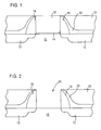
- FIG. 2 depicts the structure of FIG. 1 after the dummy gate and the gate dielectric have been removed.
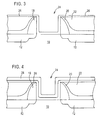
- FIG. 3 shows the semiconductor structure of FIG. 2 after a high k dielectric has been deposited.
- FIG. 4 depicts the semiconductor structure of FIG. 3 following the chemical vapor deposition of amorphous silicon over the high k gate dielectric.
- FIG. 5 illustrates the semiconductor structure of FIG. 4 after a metal has been deposited within the recess in accordance with the embodiments of the present invention.
- FIG. 6 is a cross-section of the semiconductor structure of FIG. 5 after a planarizing procedure has been performed.
- the present invention addresses and solves problems related to the use of metal gates in semiconductor structures.
- the work function has changed due to the use of metal on a silicon substrate.
- the present invention provides a work function that is at least substantially the same as the work function of a polysilicon gate on a silicon substrate. This is achieved by providing a chemically vapor deposited amorphous silicon layer over the silicon substrate.
- the metal of the gate structure is deposited on the amorphous silicon.
- the presence of the amorphous silicon between the metal gate and the silicon substrate causes the work function to be substantially the same as the work function of a polysilicon gate on a silicon substrate.
- the resistance of the gate is reduced due to the replacement of the polysilicon gate with the metal gate structure.
- FIG. 1 is a cross-section of a precursor for the semiconductor structure constructed in accordance with embodiments of the present invention.
- the features in the drawings are not necessarily represented accurately in terms of relative sizes or shapes, but have been rendered for illustrative purposes.
- the silicon substrate 10 has active regions 12 formed therein by conventional doping techniques.
- a gate oxide 14 has been provided on the surface of the substrate 10 .
- a polysilicon gate 16 which serves as a temporary (or “dummy”) gate is provided on top of the gate oxide 14 .
- Spacers 18 are provided on the sidewalls of the gate 16 .
- the sidewalls 18 may be made of material, such as silicon nitride, silicon oxide, silicon oxynitride, or different layers thereof.
- Layer 20 is an etch stop layer and/or a bottom anti-reflective coating (BARC) layer.
- BARC bottom anti-reflective coating
- a dielectric layer 22 is provided on top of the BARC layer 20 .
- the semiconductor structure of FIG. 1 has been planarized, by chemical mechanical planarization (CMP), for example, to provide a planarized upper surface.
- CMP chemical mechanical planarization
- the structure of FIG. 1 is a conventional semiconductor structure with active regions and a polysilicon gate.
- the polysilicon gate 16 may be removed and replaced by a metal gate, as provided for in the present invention.
- a metal gate structure undesirably changes the work function of the gate. This is avoided in the present invention by the use of a chemical vapor deposited amorphous silicon layer.
- the polysilicon gate 16 and gate oxide 14 have been removed from the region between spacers 18 . This leaves a recess 24 bounded by the top of the substrate 10 and the sidewalls formed by the spacers 18 .
- a plasma reactive ion etch (RIE) using chlorine or a wet polysilicon etch using conventional etch chemistry may be utilized to remove the polysilicon layer to form the opening (i.e. recess) 24 .
- a high k dielectric is provided as layer 26 within the recess 24 .
- the high k gate dielectric 26 can provided in a layer having a thickness between about 15 and about 200 Angstroms thick, for example.
- Conventional methods of deposition, such as chemical vapor deposition, may be used to deposit the high k gate dielectric layer 26 .
- Typical materials that may be used in the high k gate dielectric layer 26 include ZrO 2 , HfO 2 , InO 2 , LaO 2 , TaO 2 , for example.
- Other multiple metal oxides may be used or perovskites may be employed as the high k gate dielectric material in layer 26 .
- a reason for using high k material as a gate dielectric is that it provides better electrical coupling with the gate and the channel. Furthermore, silicon dioxide is no longer extendible. Tunneling leakage is an important consideration. With high k material, a thicker film can be used while still obtaining the same electric field.
- One of the concerns with high k material is its low temperature stability. In other words, at high temperatures, high k materials react with the silicon substrate. Processing at lower temperatures, such as with nickel silicide, mitigate this concern.
- FIG. 4 depicts the semiconductor structure of FIG. 3 after the deposition of an amorphous silicon layer 28 .
- the amorphous silicon layer 28 is provided within the recess 24 on top of the high k gate dielectric layer 26 .
- the amporhous silicon layer 28 is deposited by chemical vapor deposition or plasma enhanced chemical vapor deposition.
- the layer 28 is a CVD amorphous silicon layer or a PECVD amorphous silicon layer.
- a conventional chemical vapor deposition or plasma enhanced chemical vapor deposition process may be used to deposit the amorphous silicon layer 28 .
- the amorphous silicon is normally deposited at temperatures less than 550° C.
- Deposition is from a pure silane gas, i.e. with no additives or carriers.
- a pressure in the deposition chamber is maintained between about 100 to about 400 mT.
- the temperature is controlled between about 520 and about 550° C.
- the deposition rate is between about 10 to about 20 ⁇ /second.
- a thickness of the amorphous silicon layer 28 is between approximately 50 and approximately 500 Angstroms in certain preferred embodiments, and between approximately 50 and approximately 200 Angstroms in especially preferred embodiments.
- Such thicknesses are typically used when the final gate structure is between approximately 1000 and approximately 2000 Angstroms high.
- One of the advantages of CVD and PECVD deposition is the substantially uniform thickness provided on the sidewalls and bottom of the recess 24 due to the excellent step coverage of the CVD and the PECVD processes.
- phosphine and BF 2 are added to the silane gas to dope the CVD amorphous silicon layer to lower the resistivity of the CVD amorphous silicon layer.
- a metal layer 30 is deposited over the amorphous silicon layer 28 .
- the deposition may take place by chemical vapor deposition, for example.
- the use of a CVD deposition of the amorphous silicon, followed by the CVD deposition of the metal 30 allows both processes to be performed in situ so that the semiconductor structure does not have to be removed from the deposition chamber between the different deposition processes. This reduces processing time and handling of the wafer.
- the metal that is deposited in metal layer 30 may be any of a number of different types of metals, such as tungsten, titanium, molybdenum, nickel, etc.
- the CVD deposition of the metal layer 30 is achieved by conventional deposition techniques.
- the semiconductor structure of FIG. 5 has been planarized, by chemical mechanical planarization, for example. This presents a smooth, top surface suitable for further processing.
- the semiconductor structure now has a complete replacement gate electrode comprising the high k gate dielectric 26 , the CVD amorphous silicon 28 and the metal 30 .
- the gate structure depicted in FIG. 6 exhibits the lower resisitivity provided by a metal gate, but does not have a changed work function in comparison to a polysilcon gate due to the presence of the CVD amorphous silicon layer 28 .
- the gate structure appears electrically like a polysilicon gate. Control of the gate is therefore improved over conventional metal gates.
- the method of forming the metal gate in accordance with the present invention ensures that the metal on the gate is not subjected to high temperature processing.
Abstract
Description
Claims (10)
Priority Applications (1)
| Application Number | Priority Date | Filing Date | Title |
|---|---|---|---|
| US09/691,181 US6528362B1 (en) | 2000-10-19 | 2000-10-19 | Metal gate with CVD amorphous silicon layer for CMOS devices and method of making with a replacement gate process |
Applications Claiming Priority (1)
| Application Number | Priority Date | Filing Date | Title |
|---|---|---|---|
| US09/691,181 US6528362B1 (en) | 2000-10-19 | 2000-10-19 | Metal gate with CVD amorphous silicon layer for CMOS devices and method of making with a replacement gate process |
Publications (1)
| Publication Number | Publication Date |
|---|---|
| US6528362B1 true US6528362B1 (en) | 2003-03-04 |
Family
ID=24775475
Family Applications (1)
| Application Number | Title | Priority Date | Filing Date |
|---|---|---|---|
| US09/691,181 Expired - Lifetime US6528362B1 (en) | 2000-10-19 | 2000-10-19 | Metal gate with CVD amorphous silicon layer for CMOS devices and method of making with a replacement gate process |
Country Status (1)
| Country | Link |
|---|---|
| US (1) | US6528362B1 (en) |
Cited By (11)
| Publication number | Priority date | Publication date | Assignee | Title |
|---|---|---|---|---|
| US20050051854A1 (en) * | 2003-09-09 | 2005-03-10 | International Business Machines Corporation | Structure and method for metal replacement gate of high performance |
| US20050055494A1 (en) * | 2003-09-10 | 2005-03-10 | International Business Machines Corporation | Structure and method for silicided metal gate transistors |
| US20050136677A1 (en) * | 2003-12-18 | 2005-06-23 | Brask Justin K. | Method for making a semiconductor device that includes a metal gate electrode |
| US20050280118A1 (en) * | 2004-06-18 | 2005-12-22 | Taiwan Semiconductor Manufacturing Company, Ltd. | Methods of manufacturing metal-silicide features |
| US20060128055A1 (en) * | 2004-12-14 | 2006-06-15 | International Business Machines Corporation | Replacement gate with tera cap |
| US20090087974A1 (en) * | 2007-09-29 | 2009-04-02 | Andrew Waite | Method of forming high-k gate electrode structures after transistor fabrication |
| US20090206416A1 (en) * | 2008-02-19 | 2009-08-20 | International Business Machines Corporation | Dual metal gate structures and methods |
| US20090242936A1 (en) * | 2008-03-28 | 2009-10-01 | International Business Machines Corporation | Strained ultra-thin soi transistor formed by replacement gate |
| WO2013016852A1 (en) * | 2011-07-29 | 2013-02-07 | 中国科学院微电子研究所 | Method of fabricating semiconductor device |
| US9269634B2 (en) | 2011-05-16 | 2016-02-23 | Globalfoundries Inc. | Self-aligned metal gate CMOS with metal base layer and dummy gate structure |
| US9502416B1 (en) | 2015-06-04 | 2016-11-22 | Samsung Electronics Co., Ltd. | Semiconductor device including transistors having different threshold voltages |
Citations (8)
| Publication number | Priority date | Publication date | Assignee | Title |
|---|---|---|---|---|
| US5397909A (en) * | 1990-10-12 | 1995-03-14 | Texas Instruments Incorporated | High-performance insulated-gate field-effect transistor |
| US5960270A (en) | 1997-08-11 | 1999-09-28 | Motorola, Inc. | Method for forming an MOS transistor having a metallic gate electrode that is formed after the formation of self-aligned source and drain regions |
| US5966597A (en) * | 1998-01-06 | 1999-10-12 | Altera Corporation | Method of forming low resistance gate electrodes |
| US6033963A (en) * | 1999-08-30 | 2000-03-07 | Taiwan Semiconductor Manufacturing Company | Method of forming a metal gate for CMOS devices using a replacement gate process |
| US6054355A (en) * | 1997-06-30 | 2000-04-25 | Kabushiki Kaisha Toshiba | Method of manufacturing a semiconductor device which includes forming a dummy gate |
| US6258679B1 (en) * | 1999-12-20 | 2001-07-10 | International Business Machines Corporation | Sacrificial silicon sidewall for damascene gate formation |
| US6303418B1 (en) * | 2000-06-30 | 2001-10-16 | Chartered Semiconductor Manufacturing Ltd. | Method of fabricating CMOS devices featuring dual gate structures and a high dielectric constant gate insulator layer |
| US6368950B1 (en) * | 2000-12-12 | 2002-04-09 | Advanced Micro Devices, Inc. | Silicide gate transistors |
-
2000
- 2000-10-19 US US09/691,181 patent/US6528362B1/en not_active Expired - Lifetime
Patent Citations (8)
| Publication number | Priority date | Publication date | Assignee | Title |
|---|---|---|---|---|
| US5397909A (en) * | 1990-10-12 | 1995-03-14 | Texas Instruments Incorporated | High-performance insulated-gate field-effect transistor |
| US6054355A (en) * | 1997-06-30 | 2000-04-25 | Kabushiki Kaisha Toshiba | Method of manufacturing a semiconductor device which includes forming a dummy gate |
| US5960270A (en) | 1997-08-11 | 1999-09-28 | Motorola, Inc. | Method for forming an MOS transistor having a metallic gate electrode that is formed after the formation of self-aligned source and drain regions |
| US5966597A (en) * | 1998-01-06 | 1999-10-12 | Altera Corporation | Method of forming low resistance gate electrodes |
| US6033963A (en) * | 1999-08-30 | 2000-03-07 | Taiwan Semiconductor Manufacturing Company | Method of forming a metal gate for CMOS devices using a replacement gate process |
| US6258679B1 (en) * | 1999-12-20 | 2001-07-10 | International Business Machines Corporation | Sacrificial silicon sidewall for damascene gate formation |
| US6303418B1 (en) * | 2000-06-30 | 2001-10-16 | Chartered Semiconductor Manufacturing Ltd. | Method of fabricating CMOS devices featuring dual gate structures and a high dielectric constant gate insulator layer |
| US6368950B1 (en) * | 2000-12-12 | 2002-04-09 | Advanced Micro Devices, Inc. | Silicide gate transistors |
Non-Patent Citations (4)
| Title |
|---|
| Ducroquet et al., Full CMP Integration of CVD TiN Damascene Sub-0.1-um Metal Gate Devices for ULSI Applications, IEEE Trans. Electron Devices, 48 (Aug. 2001) 1816.* * |
| Inumiya et al., Conformable Formation of High Quality Ultra-Thin Amorphous Ta2O5 Gate Dielectrics Utilizing Water Assisted Deposition (WAD) for Sub 50 nm Damascene Metal Gate MOSFETs, IEDM 2000, 28.4.1.* * |
| Yagashita et al., High Performance Damascene Metal Gate MOSFET's for 0.1 um Regime, IEEE Trans. Electron Devices, 47 (May 2000) 1028. * |
| Yagishita et al., Improvement of Threshold Voltage Deviation in Damascene Metal Gate Transistors, IEEE Trans. Electron Devices, 48 (Aug. 2001) 1604.* * |
Cited By (27)
| Publication number | Priority date | Publication date | Assignee | Title |
|---|---|---|---|---|
| US20050051854A1 (en) * | 2003-09-09 | 2005-03-10 | International Business Machines Corporation | Structure and method for metal replacement gate of high performance |
| US6921711B2 (en) | 2003-09-09 | 2005-07-26 | International Business Machines Corporation | Method for forming metal replacement gate of high performance |
| US6908850B2 (en) | 2003-09-10 | 2005-06-21 | International Business Machines Corporation | Structure and method for silicided metal gate transistors |
| US20050055494A1 (en) * | 2003-09-10 | 2005-03-10 | International Business Machines Corporation | Structure and method for silicided metal gate transistors |
| US7160767B2 (en) * | 2003-12-18 | 2007-01-09 | Intel Corporation | Method for making a semiconductor device that includes a metal gate electrode |
| US20050136677A1 (en) * | 2003-12-18 | 2005-06-23 | Brask Justin K. | Method for making a semiconductor device that includes a metal gate electrode |
| US20050280118A1 (en) * | 2004-06-18 | 2005-12-22 | Taiwan Semiconductor Manufacturing Company, Ltd. | Methods of manufacturing metal-silicide features |
| US20070284678A1 (en) * | 2004-06-18 | 2007-12-13 | Taiwan Semiconductor Manufacturing Company, Ltd. | Methods of Manufacturing Metal-Silicide Features |
| US7268065B2 (en) | 2004-06-18 | 2007-09-11 | Taiwan Semiconductor Manufacturing Company, Ltd. | Methods of manufacturing metal-silicide features |
| US8202799B2 (en) | 2004-06-18 | 2012-06-19 | Taiwan Semiconductor Manufacturing Company, Ltd. | Methods of manufacturing metal-silicide features |
| US8791528B2 (en) | 2004-06-18 | 2014-07-29 | Taiwan Semiconductor Manufacturing Company, Ltd. | Methods of manufacturing metal-silicide features |
| US7781316B2 (en) | 2004-06-18 | 2010-08-24 | Taiwan Semiconductor Manufacturing Company, Ltd. | Methods of manufacturing metal-silicide features |
| US20100273324A1 (en) * | 2004-06-18 | 2010-10-28 | Taiwan Semiconductor Manufacturing Company, Ltd. | Methods of manufacturing metal-silicide features |
| US20100314698A1 (en) * | 2004-06-18 | 2010-12-16 | Taiwan Semiconductor Manufacturing Company, Ltd. | Methods of manufacturing metal-silicide features |
| US20060128055A1 (en) * | 2004-12-14 | 2006-06-15 | International Business Machines Corporation | Replacement gate with tera cap |
| US7138308B2 (en) | 2004-12-14 | 2006-11-21 | International Business Machines Corporation | Replacement gate with TERA cap |
| US20090087974A1 (en) * | 2007-09-29 | 2009-04-02 | Andrew Waite | Method of forming high-k gate electrode structures after transistor fabrication |
| US20090206416A1 (en) * | 2008-02-19 | 2009-08-20 | International Business Machines Corporation | Dual metal gate structures and methods |
| US7955909B2 (en) | 2008-03-28 | 2011-06-07 | International Business Machines Corporation | Strained ultra-thin SOI transistor formed by replacement gate |
| US20110121363A1 (en) * | 2008-03-28 | 2011-05-26 | International Business Machines Corporation | Strained ultra-thin soi transistor formed by replacement gate |
| US8536650B2 (en) | 2008-03-28 | 2013-09-17 | International Business Machines Corporation | Strained ultra-thin SOI transistor formed by replacement gate |
| US20090242936A1 (en) * | 2008-03-28 | 2009-10-01 | International Business Machines Corporation | Strained ultra-thin soi transistor formed by replacement gate |
| US9269634B2 (en) | 2011-05-16 | 2016-02-23 | Globalfoundries Inc. | Self-aligned metal gate CMOS with metal base layer and dummy gate structure |
| WO2013016852A1 (en) * | 2011-07-29 | 2013-02-07 | 中国科学院微电子研究所 | Method of fabricating semiconductor device |
| US8664119B2 (en) | 2011-07-29 | 2014-03-04 | Institute of Microelectronics, Chinese Academy of Sciences | Semiconductor device manufacturing method |
| US9502416B1 (en) | 2015-06-04 | 2016-11-22 | Samsung Electronics Co., Ltd. | Semiconductor device including transistors having different threshold voltages |
| US9947671B2 (en) | 2015-06-04 | 2018-04-17 | Samsung Electronics Co., Ltd. | Semiconductor device including transistors having different threshold voltages |
Similar Documents
| Publication | Publication Date | Title |
|---|---|---|
| US6392280B1 (en) | Metal gate with PVD amorphous silicon layer for CMOS devices and method of making with a replacement gate process | |
| US7071086B2 (en) | Method of forming a metal gate structure with tuning of work function by silicon incorporation | |
| US7042033B2 (en) | ULSI MOS with high dielectric constant gate insulator | |
| US7119407B2 (en) | Semiconductor device and manufacturing method thereof | |
| US7521345B2 (en) | High-temperature stable gate structure with metallic electrode | |
| KR100530401B1 (en) | Semiconductor device having a low-resistance gate electrode | |
| US6436840B1 (en) | Metal gate with CVD amorphous silicon layer and a barrier layer for CMOS devices and method of making with a replacement gate process | |
| JP2007513498A (en) | CVD Tantalum Compound for FET Gate Electrode (Chemical Vapor Deposition Method of Compounds Containing Ta and N and Semiconductor Field Effect Device) | |
| US6440868B1 (en) | Metal gate with CVD amorphous silicon layer and silicide for CMOS devices and method of making with a replacement gate process | |
| JP2006108602A (en) | Semiconductor device and its manufacturing method | |
| US6002150A (en) | Compound material T gate structure for devices with gate dielectrics having a high dielectric constant | |
| JP4239188B2 (en) | Method for manufacturing MOSFET element | |
| US20010024860A1 (en) | Method for manufacturing a gate structure incorporating therein aluminum oxide as a gate dielectric | |
| US6589866B1 (en) | Metal gate with PVD amorphous silicon layer having implanted dopants for CMOS devices and method of making with a replacement gate process | |
| US6528362B1 (en) | Metal gate with CVD amorphous silicon layer for CMOS devices and method of making with a replacement gate process | |
| US6440867B1 (en) | Metal gate with PVD amorphous silicon and silicide for CMOS devices and method of making the same with a replacement gate process | |
| KR100755121B1 (en) | Method for forming electrode structure and method for fabricating semiconductor device | |
| US6642590B1 (en) | Metal gate with PVD amorphous silicon layer and barrier layer for CMOS devices and method of making with a replacement gate process | |
| JP2004207481A (en) | Semiconductor device and its manufacturing method | |
| US7138339B2 (en) | Method of manufacturing semiconductor device including etching a conductive layer by using a gas including SiCl4 and NF3 | |
| KR20000048093A (en) | Tungsten silicide nitride as an electrode for tantalum pentoxide devices | |
| US6893910B1 (en) | One step deposition method for high-k dielectric and metal gate electrode | |
| KR100315043B1 (en) | Method of manufacturing semiconductor device having gate dielectric made of aluminium oxide | |
| KR20020047510A (en) | Method of manufacturing a transistor in a semiconductor device | |
| JP2000049340A (en) | Semiconductor device and fabrication thereof |
Legal Events
| Date | Code | Title | Description |
|---|---|---|---|
| AS | Assignment |
Owner name: ADVANCED MICRO DEVICES, INC., CALIFORNIA Free format text: ASSIGNMENT OF ASSIGNORS INTEREST;ASSIGNORS:BESSER, PAUL R.;XIANG, QI;BUYNOSKI, MATTHEW S.;REEL/FRAME:011227/0873;SIGNING DATES FROM 20001003 TO 20001016 |
|
| STCF | Information on status: patent grant |
Free format text: PATENTED CASE |
|
| FPAY | Fee payment |
Year of fee payment: 4 |
|
| AS | Assignment |
Owner name: GLOBALFOUNDRIES INC., CAYMAN ISLANDS Free format text: AFFIRMATION OF PATENT ASSIGNMENT;ASSIGNOR:ADVANCED MICRO DEVICES, INC.;REEL/FRAME:023119/0083 Effective date: 20090630 |
|
| FPAY | Fee payment |
Year of fee payment: 8 |
|
| FPAY | Fee payment |
Year of fee payment: 12 |
|
| AS | Assignment |
Owner name: WILMINGTON TRUST, NATIONAL ASSOCIATION, DELAWARE Free format text: SECURITY AGREEMENT;ASSIGNOR:GLOBALFOUNDRIES INC.;REEL/FRAME:049490/0001 Effective date: 20181127 |
|
| AS | Assignment |
Owner name: GLOBALFOUNDRIES U.S. INC., CALIFORNIA Free format text: ASSIGNMENT OF ASSIGNORS INTEREST;ASSIGNOR:GLOBALFOUNDRIES INC.;REEL/FRAME:054633/0001 Effective date: 20201022 |
|
| AS | Assignment |
Owner name: GLOBALFOUNDRIES INC., CAYMAN ISLANDS Free format text: RELEASE BY SECURED PARTY;ASSIGNOR:WILMINGTON TRUST, NATIONAL ASSOCIATION;REEL/FRAME:054636/0001 Effective date: 20201117 |
|
| AS | Assignment |
Owner name: GLOBALFOUNDRIES U.S. INC., NEW YORK Free format text: RELEASE BY SECURED PARTY;ASSIGNOR:WILMINGTON TRUST, NATIONAL ASSOCIATION;REEL/FRAME:056987/0001 Effective date: 20201117 |