US6512266B1 - Method of fabricating SiO2 spacers and annealing caps - Google Patents
Method of fabricating SiO2 spacers and annealing caps Download PDFInfo
- Publication number
- US6512266B1 US6512266B1 US09/902,830 US90283001A US6512266B1 US 6512266 B1 US6512266 B1 US 6512266B1 US 90283001 A US90283001 A US 90283001A US 6512266 B1 US6512266 B1 US 6512266B1
- Authority
- US
- United States
- Prior art keywords
- cmos device
- oxide film
- patterned gate
- comprised
- gate stack
- Prior art date
- Legal status (The legal status is an assumption and is not a legal conclusion. Google has not performed a legal analysis and makes no representation as to the accuracy of the status listed.)
- Expired - Lifetime
Links
- VYPSYNLAJGMNEJ-UHFFFAOYSA-N silicon dioxide Inorganic materials O=[Si]=O VYPSYNLAJGMNEJ-UHFFFAOYSA-N 0.000 title claims abstract description 50
- 229910052681 coesite Inorganic materials 0.000 title claims abstract description 32
- 229910052906 cristobalite Inorganic materials 0.000 title claims abstract description 32
- 239000000377 silicon dioxide Substances 0.000 title claims abstract description 32
- 229910052682 stishovite Inorganic materials 0.000 title claims abstract description 32
- 229910052905 tridymite Inorganic materials 0.000 title claims abstract description 32
- 238000000137 annealing Methods 0.000 title abstract description 33
- 238000004519 manufacturing process Methods 0.000 title description 2
- 235000012239 silicon dioxide Nutrition 0.000 title 1
- 239000004065 semiconductor Substances 0.000 claims abstract description 49
- 229910021332 silicide Inorganic materials 0.000 claims abstract description 20
- 230000000295 complement effect Effects 0.000 claims abstract description 4
- 229910044991 metal oxide Inorganic materials 0.000 claims abstract description 4
- 150000004706 metal oxides Chemical class 0.000 claims abstract description 4
- 125000006850 spacer group Chemical group 0.000 claims description 80
- 239000000463 material Substances 0.000 claims description 58
- 239000000758 substrate Substances 0.000 claims description 41
- 229910052751 metal Inorganic materials 0.000 claims description 24
- 239000002184 metal Substances 0.000 claims description 24
- 150000004767 nitrides Chemical class 0.000 claims description 15
- 229910052710 silicon Inorganic materials 0.000 claims description 11
- 229910021420 polycrystalline silicon Inorganic materials 0.000 claims description 9
- 229920005591 polysilicon Polymers 0.000 claims description 9
- 229910000577 Silicon-germanium Inorganic materials 0.000 claims description 6
- MCMNRKCIXSYSNV-UHFFFAOYSA-N Zirconium dioxide Chemical compound O=[Zr]=O MCMNRKCIXSYSNV-UHFFFAOYSA-N 0.000 claims description 6
- 229910021417 amorphous silicon Inorganic materials 0.000 claims description 6
- 150000002739 metals Chemical class 0.000 claims description 6
- 229910001218 Gallium arsenide Inorganic materials 0.000 claims description 3
- 229910000673 Indium arsenide Inorganic materials 0.000 claims description 3
- 229910045601 alloy Inorganic materials 0.000 claims description 3
- 239000000956 alloy Substances 0.000 claims description 3
- PNEYBMLMFCGWSK-UHFFFAOYSA-N aluminium oxide Inorganic materials [O-2].[O-2].[O-2].[Al+3].[Al+3] PNEYBMLMFCGWSK-UHFFFAOYSA-N 0.000 claims description 3
- 229910052593 corundum Inorganic materials 0.000 claims description 3
- 229910052732 germanium Inorganic materials 0.000 claims description 3
- RPQDHPTXJYYUPQ-UHFFFAOYSA-N indium arsenide Chemical compound [In]#[As] RPQDHPTXJYYUPQ-UHFFFAOYSA-N 0.000 claims description 3
- 239000012212 insulator Substances 0.000 claims description 3
- -1 silicon, elemental metals Chemical class 0.000 claims description 3
- PBCFLUZVCVVTBY-UHFFFAOYSA-N tantalum pentoxide Inorganic materials O=[Ta](=O)O[Ta](=O)=O PBCFLUZVCVVTBY-UHFFFAOYSA-N 0.000 claims description 3
- 229910001845 yogo sapphire Inorganic materials 0.000 claims description 3
- XUIMIQQOPSSXEZ-UHFFFAOYSA-N Silicon Chemical compound [Si] XUIMIQQOPSSXEZ-UHFFFAOYSA-N 0.000 claims 2
- 239000010703 silicon Substances 0.000 claims 2
- 206010010144 Completed suicide Diseases 0.000 claims 1
- 238000000034 method Methods 0.000 abstract description 60
- FVBUAEGBCNSCDD-UHFFFAOYSA-N silicide(4-) Chemical compound [Si-4] FVBUAEGBCNSCDD-UHFFFAOYSA-N 0.000 abstract description 18
- 238000004140 cleaning Methods 0.000 abstract description 5
- 238000005530 etching Methods 0.000 description 26
- 239000003989 dielectric material Substances 0.000 description 23
- 239000007943 implant Substances 0.000 description 13
- 238000005137 deposition process Methods 0.000 description 9
- 238000005468 ion implantation Methods 0.000 description 9
- 238000005229 chemical vapour deposition Methods 0.000 description 8
- 239000003870 refractory metal Substances 0.000 description 8
- 238000009792 diffusion process Methods 0.000 description 7
- 239000002019 doping agent Substances 0.000 description 7
- 238000000623 plasma-assisted chemical vapour deposition Methods 0.000 description 7
- 238000000151 deposition Methods 0.000 description 5
- 238000001312 dry etching Methods 0.000 description 5
- 125000001475 halogen functional group Chemical group 0.000 description 5
- IJGRMHOSHXDMSA-UHFFFAOYSA-N Atomic nitrogen Chemical compound N#N IJGRMHOSHXDMSA-UHFFFAOYSA-N 0.000 description 4
- 230000015572 biosynthetic process Effects 0.000 description 4
- 230000008021 deposition Effects 0.000 description 4
- 229920002120 photoresistant polymer Polymers 0.000 description 4
- 239000000126 substance Substances 0.000 description 4
- YCKRFDGAMUMZLT-UHFFFAOYSA-N Fluorine atom Chemical compound [F] YCKRFDGAMUMZLT-UHFFFAOYSA-N 0.000 description 3
- 238000000224 chemical solution deposition Methods 0.000 description 3
- 238000001704 evaporation Methods 0.000 description 3
- 230000008020 evaporation Effects 0.000 description 3
- 229910052731 fluorine Inorganic materials 0.000 description 3
- 239000011737 fluorine Substances 0.000 description 3
- 230000003071 parasitic effect Effects 0.000 description 3
- 238000001020 plasma etching Methods 0.000 description 3
- 229910052581 Si3N4 Inorganic materials 0.000 description 2
- 230000004913 activation Effects 0.000 description 2
- 230000004888 barrier function Effects 0.000 description 2
- 239000004020 conductor Substances 0.000 description 2
- 150000002500 ions Chemical class 0.000 description 2
- 238000001459 lithography Methods 0.000 description 2
- 229910052759 nickel Inorganic materials 0.000 description 2
- 229910052757 nitrogen Inorganic materials 0.000 description 2
- 239000000376 reactant Substances 0.000 description 2
- 229910004200 TaSiN Inorganic materials 0.000 description 1
- ATJFFYVFTNAWJD-UHFFFAOYSA-N Tin Chemical compound [Sn] ATJFFYVFTNAWJD-UHFFFAOYSA-N 0.000 description 1
- 229910052782 aluminium Inorganic materials 0.000 description 1
- 150000001875 compounds Chemical class 0.000 description 1
- 230000001747 exhibiting effect Effects 0.000 description 1
- 230000005669 field effect Effects 0.000 description 1
- 238000002513 implantation Methods 0.000 description 1
- 238000011065 in-situ storage Methods 0.000 description 1
- 238000010884 ion-beam technique Methods 0.000 description 1
- 229910052741 iridium Inorganic materials 0.000 description 1
- 238000002955 isolation Methods 0.000 description 1
- 238000000608 laser ablation Methods 0.000 description 1
- QJGQUHMNIGDVPM-UHFFFAOYSA-N nitrogen group Chemical group [N] QJGQUHMNIGDVPM-UHFFFAOYSA-N 0.000 description 1
- 230000010355 oscillation Effects 0.000 description 1
- 230000003647 oxidation Effects 0.000 description 1
- 238000007254 oxidation reaction Methods 0.000 description 1
- 229910052763 palladium Inorganic materials 0.000 description 1
- 238000000059 patterning Methods 0.000 description 1
- 238000007747 plating Methods 0.000 description 1
- 229910052697 platinum Inorganic materials 0.000 description 1
- 230000005855 radiation Effects 0.000 description 1
- 238000009877 rendering Methods 0.000 description 1
- 238000010405 reoxidation reaction Methods 0.000 description 1
- 229910052703 rhodium Inorganic materials 0.000 description 1
- 229910052707 ruthenium Inorganic materials 0.000 description 1
- 229910052814 silicon oxide Inorganic materials 0.000 description 1
- 238000004088 simulation Methods 0.000 description 1
- 229910052715 tantalum Inorganic materials 0.000 description 1
- 229910052721 tungsten Inorganic materials 0.000 description 1
- 238000003631 wet chemical etching Methods 0.000 description 1
- 238000001039 wet etching Methods 0.000 description 1
- 229910052726 zirconium Inorganic materials 0.000 description 1
Images


Classifications
-
- H—ELECTRICITY
- H01—ELECTRIC ELEMENTS
- H01L—SEMICONDUCTOR DEVICES NOT COVERED BY CLASS H10
- H01L29/00—Semiconductor devices adapted for rectifying, amplifying, oscillating or switching, or capacitors or resistors with at least one potential-jump barrier or surface barrier, e.g. PN junction depletion layer or carrier concentration layer; Details of semiconductor bodies or of electrodes thereof ; Multistep manufacturing processes therefor
- H01L29/66—Types of semiconductor device ; Multistep manufacturing processes therefor
- H01L29/66007—Multistep manufacturing processes
- H01L29/66075—Multistep manufacturing processes of devices having semiconductor bodies comprising group 14 or group 13/15 materials
- H01L29/66227—Multistep manufacturing processes of devices having semiconductor bodies comprising group 14 or group 13/15 materials the devices being controllable only by the electric current supplied or the electric potential applied, to an electrode which does not carry the current to be rectified, amplified or switched, e.g. three-terminal devices
- H01L29/66409—Unipolar field-effect transistors
- H01L29/66477—Unipolar field-effect transistors with an insulated gate, i.e. MISFET
- H01L29/66568—Lateral single gate silicon transistors
- H01L29/66575—Lateral single gate silicon transistors where the source and drain or source and drain extensions are self-aligned to the sides of the gate
- H01L29/6659—Lateral single gate silicon transistors where the source and drain or source and drain extensions are self-aligned to the sides of the gate with both lightly doped source and drain extensions and source and drain self-aligned to the sides of the gate, e.g. lightly doped drain [LDD] MOSFET, double diffused drain [DDD] MOSFET
-
- H—ELECTRICITY
- H01—ELECTRIC ELEMENTS
- H01L—SEMICONDUCTOR DEVICES NOT COVERED BY CLASS H10
- H01L21/00—Processes or apparatus adapted for the manufacture or treatment of semiconductor or solid state devices or of parts thereof
- H01L21/70—Manufacture or treatment of devices consisting of a plurality of solid state components formed in or on a common substrate or of parts thereof; Manufacture of integrated circuit devices or of parts thereof
- H01L21/77—Manufacture or treatment of devices consisting of a plurality of solid state components or integrated circuits formed in, or on, a common substrate
- H01L21/78—Manufacture or treatment of devices consisting of a plurality of solid state components or integrated circuits formed in, or on, a common substrate with subsequent division of the substrate into plural individual devices
- H01L21/82—Manufacture or treatment of devices consisting of a plurality of solid state components or integrated circuits formed in, or on, a common substrate with subsequent division of the substrate into plural individual devices to produce devices, e.g. integrated circuits, each consisting of a plurality of components
- H01L21/822—Manufacture or treatment of devices consisting of a plurality of solid state components or integrated circuits formed in, or on, a common substrate with subsequent division of the substrate into plural individual devices to produce devices, e.g. integrated circuits, each consisting of a plurality of components the substrate being a semiconductor, using silicon technology
- H01L21/8232—Field-effect technology
- H01L21/8234—MIS technology, i.e. integration processes of field effect transistors of the conductor-insulator-semiconductor type
- H01L21/8238—Complementary field-effect transistors, e.g. CMOS
- H01L21/823864—Complementary field-effect transistors, e.g. CMOS with a particular manufacturing method of the gate sidewall spacers, e.g. double spacers, particular spacer material or shape
-
- H—ELECTRICITY
- H01—ELECTRIC ELEMENTS
- H01L—SEMICONDUCTOR DEVICES NOT COVERED BY CLASS H10
- H01L29/00—Semiconductor devices adapted for rectifying, amplifying, oscillating or switching, or capacitors or resistors with at least one potential-jump barrier or surface barrier, e.g. PN junction depletion layer or carrier concentration layer; Details of semiconductor bodies or of electrodes thereof ; Multistep manufacturing processes therefor
- H01L29/66—Types of semiconductor device ; Multistep manufacturing processes therefor
- H01L29/66007—Multistep manufacturing processes
- H01L29/66075—Multistep manufacturing processes of devices having semiconductor bodies comprising group 14 or group 13/15 materials
- H01L29/66227—Multistep manufacturing processes of devices having semiconductor bodies comprising group 14 or group 13/15 materials the devices being controllable only by the electric current supplied or the electric potential applied, to an electrode which does not carry the current to be rectified, amplified or switched, e.g. three-terminal devices
- H01L29/66409—Unipolar field-effect transistors
- H01L29/66477—Unipolar field-effect transistors with an insulated gate, i.e. MISFET
- H01L29/6653—Unipolar field-effect transistors with an insulated gate, i.e. MISFET using the removal of at least part of spacer, e.g. disposable spacer
-
- H—ELECTRICITY
- H01—ELECTRIC ELEMENTS
- H01L—SEMICONDUCTOR DEVICES NOT COVERED BY CLASS H10
- H01L29/00—Semiconductor devices adapted for rectifying, amplifying, oscillating or switching, or capacitors or resistors with at least one potential-jump barrier or surface barrier, e.g. PN junction depletion layer or carrier concentration layer; Details of semiconductor bodies or of electrodes thereof ; Multistep manufacturing processes therefor
- H01L29/66—Types of semiconductor device ; Multistep manufacturing processes therefor
- H01L29/66007—Multistep manufacturing processes
- H01L29/66075—Multistep manufacturing processes of devices having semiconductor bodies comprising group 14 or group 13/15 materials
- H01L29/66227—Multistep manufacturing processes of devices having semiconductor bodies comprising group 14 or group 13/15 materials the devices being controllable only by the electric current supplied or the electric potential applied, to an electrode which does not carry the current to be rectified, amplified or switched, e.g. three-terminal devices
- H01L29/66409—Unipolar field-effect transistors
- H01L29/66477—Unipolar field-effect transistors with an insulated gate, i.e. MISFET
- H01L29/6656—Unipolar field-effect transistors with an insulated gate, i.e. MISFET using multiple spacer layers, e.g. multiple sidewall spacers
-
- H—ELECTRICITY
- H01—ELECTRIC ELEMENTS
- H01L—SEMICONDUCTOR DEVICES NOT COVERED BY CLASS H10
- H01L29/00—Semiconductor devices adapted for rectifying, amplifying, oscillating or switching, or capacitors or resistors with at least one potential-jump barrier or surface barrier, e.g. PN junction depletion layer or carrier concentration layer; Details of semiconductor bodies or of electrodes thereof ; Multistep manufacturing processes therefor
- H01L29/66—Types of semiconductor device ; Multistep manufacturing processes therefor
- H01L29/68—Types of semiconductor device ; Multistep manufacturing processes therefor controllable by only the electric current supplied, or only the electric potential applied, to an electrode which does not carry the current to be rectified, amplified or switched
- H01L29/76—Unipolar devices, e.g. field effect transistors
- H01L29/772—Field effect transistors
- H01L29/78—Field effect transistors with field effect produced by an insulated gate
- H01L29/7833—Field effect transistors with field effect produced by an insulated gate with lightly doped drain or source extension, e.g. LDD MOSFET's; DDD MOSFET's
-
- H—ELECTRICITY
- H01—ELECTRIC ELEMENTS
- H01L—SEMICONDUCTOR DEVICES NOT COVERED BY CLASS H10
- H01L29/00—Semiconductor devices adapted for rectifying, amplifying, oscillating or switching, or capacitors or resistors with at least one potential-jump barrier or surface barrier, e.g. PN junction depletion layer or carrier concentration layer; Details of semiconductor bodies or of electrodes thereof ; Multistep manufacturing processes therefor
- H01L29/66—Types of semiconductor device ; Multistep manufacturing processes therefor
- H01L29/66007—Multistep manufacturing processes
- H01L29/66075—Multistep manufacturing processes of devices having semiconductor bodies comprising group 14 or group 13/15 materials
- H01L29/66227—Multistep manufacturing processes of devices having semiconductor bodies comprising group 14 or group 13/15 materials the devices being controllable only by the electric current supplied or the electric potential applied, to an electrode which does not carry the current to be rectified, amplified or switched, e.g. three-terminal devices
- H01L29/66409—Unipolar field-effect transistors
- H01L29/66477—Unipolar field-effect transistors with an insulated gate, i.e. MISFET
- H01L29/665—Unipolar field-effect transistors with an insulated gate, i.e. MISFET using self aligned silicidation, i.e. salicide
Definitions
- the present invention relates to complementary metal oxide semiconductor (CMOS) devices, and more particularly to metal oxide semiconductor field effect transistors (MOSFETs) that include an oxide spacer to reduce parasitic capacitance and an annealing cap that prevents dopant loss in the gate material during an activation-annealing step.
- CMOS complementary metal oxide semiconductor
- MOSFETs metal oxide semiconductor field effect transistors
- the present invention also provides methods of manufacturing the CMOS devices of the present invention.
- SiN spacers are typically used to implant source/drain extensions (SDE) and halos for CMOS devices.
- SDE source/drain extensions
- the use of SiO 2 spacers is advantageous compared to SiN spacers because the lower dielectric constant of SiO 2 reduces the parasitic capacitance between the gate and S/D regions.
- Annealing caps are used to protect the patterned gate stack, source/drain (S/D) and SDE regions from dopant loss during activation annealing.
- the utilization of a deposited oxide material as the annealing cap is advantageous since low energy implantation can be performed through the bare Si substrate. After the implant, a low temperature SiO 2 film may be deposited over the entire wafer to prevent dopant loss during annealing.
- the SiO 2 cap also serves as an etch stop for the thicker SiN spacer formation used to implant the S/D regions. As in the case of the thin SiO 2 spacer, the SiO 2 annealing cap reduces the parasitic capacitance between the gate and S/D regions. Simulations have shown that switching from a nitride annealing cap to an oxide annealing cap improves the ring oscillation delay by as much as 5%.
- a major problem of integrating thin SiO 2 spacers and/or SiO 2 annealing caps into prior art processes is that any SiO 2 that is exposed during the pre-silicide cleaning or other process steps may be excessively etched.
- any SiO 2 that is exposed during the pre-silicide cleaning or other process steps may be excessively etched.
- excessive etching may cause the entire SiO 2 spacer to be removed thus leaving Si substrate area exposed. This leads to gate to substrate shorting by silicide bridging.
- the SiO 2 annealing cap if the etching is excessive then the thick SiN spacers are undercut and may become completely detached rendering the device inoperable. This leads to silicide bridging since the spacers are present to prevent this from occurring.
- One object of the present invention is to provide a method of forming a CMOS device in which a thin SiO 2 spacer and/or annealing cap is employed.
- Another object of the present invention is to provide a method of forming a CMOS device in which the thin SiO 2 spacer and/or annealing cap is not aggressively attacked during the silicide pre-cleaning step or other process.
- the divot fill process provides a means for protecting the exposed surfaces of the thin SiO 2 spacer and/or annealing cap such that those surfaces are not capable of being attacked by a subsequent silicide pre-cleaning or other process steps.
- a first method of the present invention which forms an SiO 2 annealing cap, comprises the steps of:
- said semiconductor structure comprises at least a semiconductor substrate having at least one patterned gate stack region formed thereon;
- the oxide film remaining in the structure after the recessing step is in the shape of the letter “L”.
- the oxide film remaining in the structure after recessing is present on portions of the vertical sidewalls of the patterned gate stack region as well as on a portion of the semiconductor substrate.
- the first method of the present invention provides a CMOS device which comprises:
- a semiconductor structure having at least one patterned gate stack region formed thereon, said patterned gate stack region having vertical sidewalls;
- thick spacers formed on said oxide film, wherein said thick spacers extend beyond edges of said oxide film such that a divot region is present between at least said thick spacers and a top surface of said patterned gate stack region;
- a second method of the present invention which forms a thin SiO 2 spacer and/or annealing cap comprises the steps of:
- said semiconductor structure comprises at least a semiconductor substrate having at least one patterned gate stack region formed thereon;
- the second method of the present invention provides a CMOS device which comprises:
- a semiconductor structure having at least one patterned gate stack region formed thereon, said patterned gate stack region having vertical sidewalls;
- thick spacers formed on said oxide film and said semiconductor substrate, wherein said thick spacers extend beyond edges of said oxide film such that a divot region is present between at least said thick spacers and a top surface of said patterned gate stack region;
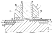
- FIGS. 1A-1F are pictorial representations (through cross-sectional views) illustrating the inventive CMOS device through various processing steps employed in the first method of the present invention.
- FIGS. 2A-2G are pictorial representations (through cross-sectional views) illustrating the inventive CMOS device through various processing steps employed in a second method of the present invention.
- FIG. 1A illustrates an initial structure that is employed in the present invention.
- the initial structure shown in FIG. 1A comprises semiconductor substrate 10 , patterned gate dielectric 12 formed on a portion of semiconductor substrate 10 , and patterned gate stack 14 formed atop patterned gate dielectric 12 .
- patterned gate dielectric 12 formed on a portion of semiconductor substrate 10
- patterned gate stack 14 formed atop patterned gate dielectric 12 .
- semiconductor substrate 10 is comprised of a semiconductor material including, but not limited to: Si, Ge, SiGe, GaAs, InAs, InP and all other III/V semiconductor compounds.
- semiconductor substrate 10 may also include a layered substrate comprising the same or different semiconductor material, e.g., Si/Si or Si/SiGe, as well as a silicon-on-insulator (SOI) substrate.
- the substrate may be of the n- or p-type depending on the desired device to be fabricated.
- semiconductor substrate 10 may contain active device regions, wiring regions, isolation regions or other like regions that are typically present in CMOS-containing devices. For clarity, these regions are not shown in the drawings, but are nevertheless meant to be included within region 10 .
- semiconductor substrate 10 is comprised of Si.
- a layer of gate dielectric material such as an oxide, nitride, oxynitride or any combination and multilayer thereof is then formed on a surface of semiconductor substrate 10 utilizing a conventional process well known in the art.
- the layer of gate dielectric material may be formed utilizing a conventional deposition process such as chemical vapor deposition (CVD), plasma-assisted CVD, evaporation or chemical solution deposition, or alternatively, the gate dielectric material may be formed by a thermal growing process such as oxidation, nitridation or oxynitridation. It is noted that the gate dielectric material will be subsequently patterned and etched into patterned gate dielectric 12 shown in FIG. 1 A.
- the thickness of the layer of gate dielectric material is not critical to the present invention, but typically, the gate dielectric material has a thickness of from about 1 to about 20 nm after deposition, with a thickness of from about 1.5 to about 10 nm being more highly preferred.
- the gate dielectric material employed in the present invention may be a conventional dielectric material such as SiO 2 or Si 3 N 4 , or alternatively, high-k dielectrics such as oxides of Ta, Zr, Al or combinations thereof may be employed.
- gate dielectric 12 is comprised of an oxide such as SiO 2 , ZrO 2 , Ta 2 O 5 or Al 2 O 3 .
- gate stack 14 which includes at least a gate material is formed on the gate dielectric material.
- gate material denotes a conductive material, a material that can be made conductive via a subsequent process such as ion implantation, or any combination thereof.
- suitable gate materials include, but are not limited to: polysilicon, amorphous silicon, elemental metals that are conductive such as W, Pt, Pd, Ru, Rh and Ir, alloys of these elemental metals, silicide or nitrides of these elemental metals and combinations thereof, e.g., a gate stack including a layer of polysilicon and a layer of conductive metal.
- a highly preferred gate material employed in the present invention is a gate material that is comprised of polysilicon or amorphous silicon.
- the gate material is formed on the surface of the gate dielectric material utilizing a conventional deposition process including, but not limited to: CVD, plasma-assisted CVD, evaporation, plating or chemical solution deposition.
- a conventional silicide process may be used in forming the silicide layer.
- One such silicide process that can be used in the present invention includes the steps of: first forming an elemental metal on the gate dielectric material, annealing the layers so as to form a metal silicide layer therefrom, and removing any unreacted elemental metal utilizing a conventional wet etch process that has a high selectivity for removing elemental metal as compared to silicide.
- the polysilicon layer may be formed utilizing an in-situ doping deposition process or by a conventional deposition process followed by ion implantation. Note that the ion implantation step may be formed immediately after deposition of the polysilicon layer, or in a later step of the present invention, i.e., after patterning of the gate stack.
- an optional diffusion barrier (not shown in the drawings) may be formed between each layer of the gate stack.
- the optional diffusion barrier which is formed utilizing a conventional deposition process such as CVD or plasma-assisted CVD, is comprised of a material such as SiN, TaN, TaSiN, WN, TiN, and other like materials which can prevent diffusion of a conductive material therethrough.
- the gate stack and the gate dielectric are then patterned utilizing conventional processing steps well known in the art which are capable of forming the patterned structure shown in FIG. 1 A. Specifically, the structure shown in FIG. 1A is formed by lithography and etching.
- the lithography step includes the following: applying a photoresist (not shown in the drawings) to the top surface of the gate stack, exposing the photoresist to a pattern of radiation and developing the pattern utilizing a conventional resist developer solution.
- Etching is performed utilizing a conventional dry etching process such as reactive-ion etching, plasma etching, ion beam etching, laser ablation or a combination thereof.
- the etching step may remove portions of the gate stack and the underlying gate dielectric material that are not protected by the patterned photoresist in a single step, or alternatively, multiple etching steps may be performed wherein the exposed portions of the gate stack is first removed stopping on a surface of the gate dielectric material, and thereafter the exposed portions of the gate dielectric are removed stopping on the surface of semiconductor substrate 10 .
- the patterned photoresist is removed utilizing a conventional stripping process well known in the art providing the structure shown, for example, in FIG. 1 A.
- source/drain extension and halo implants may be performed.
- region 18 denotes the source/drain extension regions and region 20 denotes the halo implant region.
- the source/drain extension and halo implant implants may be formed after the structure shown in FIG. 1B is formed.
- the deep source/drain diffusion regions (labeled as 16 in FIG. 1C) are formed utilizing conventional processes (i.e., ion implantation and annealing) anytime after the structure shown in FIG. 1C is formed, i.e., after thick spacers 24 are formed in the structure.
- the structure illustrated in FIG. 1A is subjected to a conventional reoxidation process prior to proceeding to the next step of the present invention.
- FIG. 1B illustrates the structure after oxide film 22 is formed over the patterned gate stack structure of FIG. 1 A.
- the oxide film which is the annealing cap or thin inner spacer of the inventive structure, is formed utilizing any conformal deposition process that is capable of depositing a film that follows the contour of the structure shown in FIG. 1 A.
- CVD plasma-assisted CVD, evaporation or chemical solution deposition may be employed in forming oxide film 22 on the structure.
- fluorine or nitrogen-containing dopants may be incorporated (via ion implantation or another conventional process) into oxide film 22 so as to alter the dielectric constant of oxide film 22 .
- a highly preferred oxide film employed in the present invention is a film that is comprised of SiO 2 , which may or may not be doped with fluorine or nitrogen.
- oxide film 22 is not critical to the present invention, but typically oxide film 22 has a thickness of from about 2 ⁇ to about 40 nm, with a thickness of from about 5 to about 10 nm being more highly preferred.
- an annealing step may be performed to activate the dopants, if implanted, and to possibly heal the implant damage.
- the activation-annealing step is conducted utilizing conditions well known in the art. For example, activation annealing at a temperature of about 900° C. or greater for a time period of about 30 seconds or less may be employed at this point of the present invention. Additionally, the various implants steps mentioned hereinabove may also be performed at this point of the present invention.
- thick spacers 24 which may include a single spacer material or a combination of spacer materials, are formed on the oxide film that abuts the patterned gate stack so as to provide the structure shown in FIG. 1 C.
- the thick spacers are formed of a dielectric material other than an oxide.
- the thick spacers are comprised of a nitride, an oxynitride or combinations and multilayers thereof.
- the thick spacers are formed by a conventional deposition process such as CVD or plasma-assisted CVD, followed by etching.
- the thick spacers are comprised of a combination of spacer materials
- the spacer materials may be deposited sequentially followed by a single etching step, or alternatively, one spacer material is first deposited and etched, and thereafter a second spacer material is deposited and etched. This combination of spacer material deposition and etching may be repeated any number of times.
- the etching step used in forming thick spacers 24 is a highly anisotropic etching process which is capable of removing the spacer material from atop the oxide layer that lays above the patterned gate stack.
- thick spacers is used herein to denote spacers that have a thickness of from about 2 to about 100 nm, with a thickness of from about 20 to about 80 nm being more highly preferred.
- the deep source/drain diffusion regions may be formed by utilizing conventional ion implantation and annealing processes well known in the art.
- the structure shown in FIG. 1C is then subjected to an etching step wherein oxide film 22 is recessed below the uppermost horizontal edge of thick spacers 24 providing the structure shown, for example, in FIG. 1 D.
- an etching step is employed in the present invention so as to provide divot regions 26 which exist between the thick spacers 24 and patterned gate stack 14 .
- the recessing process may be conducted laterally providing divot region 26 between the thick spacers and semiconductor substrate 10 . Note this recessing step converts oxide film 22 into an L-shaped structures 23 .
- the etching process used in forming divots 26 in the structure includes a wet chemical etch process or a dry chemical etch process.
- a chemical etchant such as HF that has a high selectivity for removing portions of the oxide film as compared with either the thick spacer material, the patterned gate stack and the semiconductor substrate is employed.
- the dry etching process includes any dry etch process which is also capable of selectively removing portions of the oxide film as compared with either the thick spacer material, the patterned gate stack and the semiconductor substrate is employed.
- divot fill material 28 is formed by a conformal deposition process such as CVD or plasma-assisted CVD so as to provide the structure shown, for example, in FIG. 1 E.
- the divot fill material includes a dielectric material other than an oxide, e.g., nitride, or oxynitride, that is not capable of being removed by a subsequent silicide precleaning or other processes which follow the processing steps of the present invention.
- the thickness of the divot fill material is not critical to the present invention, but typically the thickness of the divot fill material is from about 4 to about 80 nm with a thickness of from about 10 to about 20 nm being more highly preferred.
- the divot fill material is next etched back by utilizing a spacer type etching process or a combination of isotropic and anisotropic etches that removes the divot fill material from horizontal surfaces and possibly removes some of the divot fill material from the vertical surfaces so that the divot fill material is left completely or partially covering the recessed oxide film (both on the vertical and lateral portions).
- the etch back step results in the formation of the structure shown in FIG. 1 F.
- the silicidation process is performed after the structure illustrated in FIG. 1F is formed. Specifically, the silicidation process includes the steps of forming a refractory metal such as Co, Ni or Ti on the surface of semiconductor substrate 10 , annealing the refractory metal under conditions that are capable of converting the refractory metal layer into a metal silicide layer, and, if needed, removing any non-reactant refractory metal from the structure.
- a refractory metal such as Co, Ni or Ti
- the present invention also contemplates other well known CMOS processing steps that are typically employed in the prior art.
- the present invention also contemplates forming a metal contact to the metal silicide layer, and connecting the metal contact to an external contact.
- FIGS. 2A-2G illustrate a second method of the present invention wherein an “I” shaped oxide film is employed as an extension and halo spacer.
- FIG. 2A shows an initial structure that is employed in the second method of the present application.
- the initial structure includes semiconductor substrate 10 , patterned gate dielectric 12 formed on a portion of semiconductor substrate 10 , and patterned gate stack 14 formed atop patterned gate dielectric 12 .
- FIG. 2A the initial structure shown in FIG. 2A is identical to the one shown in FIG. 1A therefore no further details concerning the initial structure is needed herein. That is, the detailed description concerning the various elements of the structure shown in FIG. 2A as well as the processing steps used in forming the same are identical to that previously described in connection with FIG. 1A; therefore the above description regarding FIG. 1A is incorporated herein by reference.
- various ion implantation steps may be performed to implant source/drain extension regions and halo implant regions into the semiconductor substrate. Note that these implant regions are shown in FIG. 2 A.
- the various implant steps may be postponed until after the structures shown in FIGS. 2B or 2 C have been formed.
- the deep source/drain diffusion regions are again formed anytime after spacers 24 are present on the structure, i.e., after the formation of the structure shown in FIG. 2 D.
- FIG. 2B shows the structure that is obtained after oxide film 22 is formed over the patterned gate region as well as the exposed surface of semiconductor substrate 10 .
- oxide film 22 may include dopant ions such as nitrogen or fluorine incorporated therein via ion implantation so as to provide an oxide layer that has a modified dielectric constant.
- oxide film 22 is comprised of SiO 2 , which may or may not include dopant ions incorporated therein.
- oxide film 22 is formed by a conventional deposition processes such as CVD and plasma-assisted CVD which are capable of forming a conformal oxide film on the structure.
- the thickness of oxide film 22 is not critical to the present invention, but typically oxide film 22 has a thickness of from about 2 to about 30 nm, with a thickness of from about 5 to about 15 nm being more highly preferred.
- a spacer etch step is performed so as to provide the structure shown in FIG. 2 C.
- the spacer etch forms “I” shaped oxide film 25 on the structure.
- a spacer etching step is performed so as to convert oxide film 22 into “I” shaped spacers 25 which are present on at least a portion of the vertical sidewalls of the patterned gate stack. Note that in FIG. 2C, the I-shaped oxide spacers are not present on the upper portion of the patterned gate stack.
- the I-shaped oxide spacers are formed by utilizing an etching process that is highly anisotropic so that the dielectric film is removed from all horizontal surfaces, but still remains on substantially all the vertical surfaces.
- a conventional reactive ion etching process or any other like dry etching process may be utilized in etching oxide film 22 into I-shaped oxide spacers 25 .
- thick spacers 24 which may be comprised of a single spacer material or a combination of spacer materials, are formed on the structure such that the structure shown in FIG. 2D is formed.
- the thick spacers are comprised of a dielectric material, such as a nitride, or an oxynitride, which is different from I-shaped oxide spacers 25 .
- the thin spacers are comprised of SiO 2
- the thick spacers are formed of a nitride (e.g., Si 3 N 4 ) or oxynitride (e.g., SiON).
- thick spacers 24 are formed utilizing the processing steps mentioned hereinabove, e.g., deposition and etching.
- deep source/drain diffusion regions 16 may be formed in the substrate (for either NFET, PFET or both) utilizing conventional ion implantation and annealing processes well known to those skilled in the art.
- FIG. 2E shows the structure wherein I-shaped oxide spacers 25 are recessed to a level below that of the thick spacers so as to form divot region 26 in the structure.
- the oxide spacer recessing step may be carried out by a wet chemical etching process which includes the use of a chemical etch such as HF that has a high selectivity for recessing oxide spacer 25 as compared with thick spacer 24 . Note that the I-shaped spacers are recessed below the top most edge of the thick spacers.
- the recess may also be achieved by utilizing a dry etching process that is capable of etching oxide spacer 25 but is selective to the gate stack material, the thick spacers and the semiconductor substrate.
- FIG. 2F shows the structure that is obtained after divot fill material 28 is formed on all exposed surfaces of the structure.
- the divot fill material includes the same material as mentioned previously in respect to the first method of the present invention and it is formed utilizing one of the above mentioned processing steps.
- FIG. 2G shows the structure that is obtained after the divot fill material has been subjected to the above-mentioned etch back process.
- the etch back process may include a spacer type etching process or a combination of isotropic etching and anisotropic etching that removes some of the material from the vertical surfaces so that the divot fill material is left completely or partially covering oxide spacers 25 .
- the silicidation process is performed after the structure illustrated in FIG. 2G is formed. Specifically, the silicidation process includes the steps of forming a refractory metal such as Co, Ni or Ti on the surface of semiconductor substrate 10 , annealing the refractory metal under conditions that are capable of converting the refractory metal layer into a metal silicide layer, and, if needed, removing any non-reactant refractory metal from the structure.
- a refractory metal such as Co, Ni or Ti
- the present invention also contemplates other well known complementary oxide semiconductor (CMOS) processing steps that are typically employed in the prior art.
- CMOS complementary oxide semiconductor
- the present invention also contemplates forming a metal contact to the metal silicide layer, and connecting the metal contact to an external contact.
Abstract
Description
Claims (24)
Priority Applications (1)
| Application Number | Priority Date | Filing Date | Title |
|---|---|---|---|
| US09/902,830 US6512266B1 (en) | 2001-07-11 | 2001-07-11 | Method of fabricating SiO2 spacers and annealing caps |
Applications Claiming Priority (1)
| Application Number | Priority Date | Filing Date | Title |
|---|---|---|---|
| US09/902,830 US6512266B1 (en) | 2001-07-11 | 2001-07-11 | Method of fabricating SiO2 spacers and annealing caps |
Publications (2)
| Publication Number | Publication Date |
|---|---|
| US20030011080A1 US20030011080A1 (en) | 2003-01-16 |
| US6512266B1 true US6512266B1 (en) | 2003-01-28 |
Family
ID=25416463
Family Applications (1)
| Application Number | Title | Priority Date | Filing Date |
|---|---|---|---|
| US09/902,830 Expired - Lifetime US6512266B1 (en) | 2001-07-11 | 2001-07-11 | Method of fabricating SiO2 spacers and annealing caps |
Country Status (1)
| Country | Link |
|---|---|
| US (1) | US6512266B1 (en) |
Cited By (23)
| Publication number | Priority date | Publication date | Assignee | Title |
|---|---|---|---|---|
| US20030170958A1 (en) * | 2002-03-05 | 2003-09-11 | Mitsubishi Denki Kabushiki Kaisha | Method of manufacturing semiconductor device |
| US20040005750A1 (en) * | 2002-02-07 | 2004-01-08 | Taiwan Semiconductor Manufacturing Company | Approach to prevent spacer undercut by low temperature nitridation |
| US20040063289A1 (en) * | 2002-09-30 | 2004-04-01 | Fujitsu Limited | Reduction in source-drain resistance of semiconductor device |
| US6734072B1 (en) * | 2003-03-05 | 2004-05-11 | Chartered Semiconductor Manufacturing Ltd. | Method of fabricating a MOSFET device using a spike rapid thermal oxidation procedure |
| US6812105B1 (en) * | 2003-07-16 | 2004-11-02 | International Business Machines Corporation | Ultra-thin channel device with raised source and drain and solid source extension doping |
| US20050012142A1 (en) * | 2003-06-06 | 2005-01-20 | Hiroaki Hazama | Nonvolatile semiconductor memory device and manufacturing method therefor |
| US20050019998A1 (en) * | 2003-07-25 | 2005-01-27 | Chien-Chao Huang | Semiconductor device with modified channel compressive stress and the method for making same |
| US20050127410A1 (en) * | 2002-07-25 | 2005-06-16 | Dongbu Electronics Col., Ltd. | Method of making a MOS transistor |
| US20050139938A1 (en) * | 2003-12-27 | 2005-06-30 | Dongbuanam Semiconductor Inc. | Semiconductor device and method of manufacturing the same |
| US20050164460A1 (en) * | 2004-01-23 | 2005-07-28 | Agency For Science, Technology And Research | Salicide process for metal gate CMOS devices |
| US6936512B2 (en) | 2002-09-27 | 2005-08-30 | International Business Machines Corporation | Semiconductor method and structure for simultaneously forming a trench capacitor dielectric and trench sidewall device dielectric |
| US20050212040A1 (en) * | 2004-03-25 | 2005-09-29 | Kabushiki Kaisha Toshiba | Semiconductor device having gate sidewall structure in silicide process and producing method of the semiconductor device |
| US20060094194A1 (en) * | 2004-11-04 | 2006-05-04 | Taiwan Semiconductor Manufacturing Company, Ltd. | Advanced disposable spacer process by low-temperature high-stress nitride film for sub-90NM CMOS technology |
| US20070037336A1 (en) * | 2005-08-12 | 2007-02-15 | Samsung Electronics Co., Ltd. | Semiconductor device with improved gate resistance and method of its manufacture |
| US20070122958A1 (en) * | 2005-11-30 | 2007-05-31 | Fang C C | Spacer barrier structure to prevent spacer voids and method for forming the same |
| US20070122988A1 (en) * | 2005-11-29 | 2007-05-31 | International Business Machines Corporation | Methods of forming semiconductor devices using embedded l-shape spacers |
| US20070196972A1 (en) * | 2006-02-22 | 2007-08-23 | Fujitsu Limited | Semiconductor device having carrier mobility raised by generating strain in channel region and its manufacture method |
| US20080116493A1 (en) * | 2006-11-17 | 2008-05-22 | Adkisson James W | Multi-layer spacer with inhibited recess/undercut and method for fabrication thereof |
| US7393738B1 (en) | 2007-01-16 | 2008-07-01 | International Business Machines Corporation | Subground rule STI fill for hot structure |
| US20080230815A1 (en) * | 2007-03-21 | 2008-09-25 | Texas Instruments Inc. | Mitigation of gate to contact capacitance in CMOS flow |
| US20130049142A1 (en) * | 2011-08-26 | 2013-02-28 | Globalfoundries Inc. | Transistor with reduced parasitic capacitance |
| CN102976264A (en) * | 2012-12-13 | 2013-03-20 | 中国科学院物理研究所 | Method for preparing self-supporting multilayer micro nano structure |
| US10868143B2 (en) * | 2013-12-05 | 2020-12-15 | Taiwan Semiconductor Manufacturing Company, Ltd. | Spacers with rectangular profile and methods of forming the same |
Families Citing this family (21)
| Publication number | Priority date | Publication date | Assignee | Title |
|---|---|---|---|---|
| US20030098489A1 (en) * | 2001-11-29 | 2003-05-29 | International Business Machines Corporation | High temperature processing compatible metal gate electrode for pFETS and methods for fabrication |
| US6855606B2 (en) * | 2003-02-20 | 2005-02-15 | Taiwan Semiconductor Manufacturing Company, Ltd. | Semiconductor nano-rod devices |
| US6844238B2 (en) * | 2003-03-26 | 2005-01-18 | Taiwan Semiconductor Manufacturing Co., Ltd | Multiple-gate transistors with improved gate control |
| US7074656B2 (en) * | 2003-04-29 | 2006-07-11 | Taiwan Semiconductor Manufacturing Company, Ltd. | Doping of semiconductor fin devices |
| US7005330B2 (en) * | 2003-06-27 | 2006-02-28 | Taiwan Semiconductor Manufacturing Company, Ltd. | Structure and method for forming the gate electrode in a multiple-gate transistor |
| DE10335100B4 (en) * | 2003-07-31 | 2008-06-05 | Advanced Micro Devices, Inc., Sunnyvale | A method of fabricating truncated sidewall spacers for a polysilicon line and method of fabricating a field effect transistor |
| US6991979B2 (en) * | 2003-09-22 | 2006-01-31 | International Business Machines Corporation | Method for avoiding oxide undercut during pre-silicide clean for thin spacer FETs |
| US20050104142A1 (en) * | 2003-11-13 | 2005-05-19 | Vijav Narayanan | CVD tantalum compounds for FET get electrodes |
| DE10361635B4 (en) * | 2003-12-30 | 2010-05-06 | Advanced Micro Devices, Inc., Sunnyvale | A method of manufacturing a spacer element for a line element by applying an etch stop layer applied by a high directional deposition technique and a spacer transistor |
| US7452778B2 (en) * | 2004-06-10 | 2008-11-18 | Taiwan Semiconductor Manufacturing Company, Ltd. | Semiconductor nano-wire devices and methods of fabrication |
| US7078285B1 (en) | 2005-01-21 | 2006-07-18 | Sony Corporation | SiGe nickel barrier structure employed in a CMOS device to prevent excess diffusion of nickel used in the silicide material |
| US7179715B2 (en) * | 2005-03-22 | 2007-02-20 | Taiwan Semiconductor Manufacturing Co., Ltd. | Method for controlling spacer oxide loss |
| CN101237902B (en) | 2005-06-06 | 2012-02-29 | 雷斯梅德有限公司 | Mask system |
| US7495280B2 (en) * | 2006-05-16 | 2009-02-24 | Taiwan Semiconductor Manufacturing Company, Ltd. | MOS devices with corner spacers |
| US20080230839A1 (en) * | 2007-03-23 | 2008-09-25 | Joern Regul | Method of producing a semiconductor structure |
| US20080272438A1 (en) * | 2007-05-02 | 2008-11-06 | Doris Bruce B | CMOS Circuits with High-K Gate Dielectric |
| US7955964B2 (en) * | 2008-05-14 | 2011-06-07 | Taiwan Semiconductor Manufacturing Company, Ltd. | Dishing-free gap-filling with multiple CMPs |
| US8048752B2 (en) | 2008-07-24 | 2011-11-01 | Taiwan Semiconductor Manufacturing Company, Ltd. | Spacer shape engineering for void-free gap-filling process |
| US9941388B2 (en) * | 2014-06-19 | 2018-04-10 | Globalfoundries Inc. | Method and structure for protecting gates during epitaxial growth |
| FR3046290B1 (en) * | 2015-12-23 | 2019-09-20 | Commissariat A L'energie Atomique Et Aux Energies Alternatives | METHOD FOR PRODUCING SPACERS WITH LOW PERMITTIVITY |
| US20230178633A1 (en) | 2021-12-08 | 2023-06-08 | Taiwan Semiconductor Manufacturing Company, Ltd. | Self-filling spacer structure |
Citations (10)
| Publication number | Priority date | Publication date | Assignee | Title |
|---|---|---|---|---|
| US5880500A (en) | 1995-07-05 | 1999-03-09 | Sharp Kabushiki Kaisha | Semiconductor device and process and apparatus of fabricating the same |
| US5895246A (en) * | 1997-09-29 | 1999-04-20 | Lg Semicon Co., Ltd. | Method of making semiconductor device with air gap between the gate electrode and substrate during processing |
| US5936279A (en) * | 1997-10-20 | 1999-08-10 | United Microelectronics Corp. | Method of fabricating self-align contact window with silicon nitride side wall |
| US6010954A (en) | 1997-07-11 | 2000-01-04 | Chartered Semiconductor Manufacturing, Ltd. | Cmos gate architecture for integration of salicide process in sub 0.1 . .muM devices |
| US6034388A (en) | 1998-05-15 | 2000-03-07 | International Business Machines Corporation | Depleted polysilicon circuit element and method for producing the same |
| US6087706A (en) | 1998-04-07 | 2000-07-11 | Advanced Micro Devices, Inc. | Compact transistor structure with adjacent trench isolation and source/drain regions implanted vertically into trench walls |
| US6121100A (en) | 1997-12-31 | 2000-09-19 | Intel Corporation | Method of fabricating a MOS transistor with a raised source/drain extension |
| US6127712A (en) * | 1998-05-22 | 2000-10-03 | Texas Instruments--Acer Incorporated | Mosfet with buried contact and air-gap gate structure |
| US6153485A (en) | 1998-11-09 | 2000-11-28 | Chartered Semiconductor Manufacturing Ltd. | Salicide formation on narrow poly lines by pulling back of spacer |
| US6160299A (en) | 1997-08-29 | 2000-12-12 | Texas Instruments Incorporated | Shallow-implant elevated source/drain doping from a sidewall dopant source |
-
2001
- 2001-07-11 US US09/902,830 patent/US6512266B1/en not_active Expired - Lifetime
Patent Citations (10)
| Publication number | Priority date | Publication date | Assignee | Title |
|---|---|---|---|---|
| US5880500A (en) | 1995-07-05 | 1999-03-09 | Sharp Kabushiki Kaisha | Semiconductor device and process and apparatus of fabricating the same |
| US6010954A (en) | 1997-07-11 | 2000-01-04 | Chartered Semiconductor Manufacturing, Ltd. | Cmos gate architecture for integration of salicide process in sub 0.1 . .muM devices |
| US6160299A (en) | 1997-08-29 | 2000-12-12 | Texas Instruments Incorporated | Shallow-implant elevated source/drain doping from a sidewall dopant source |
| US5895246A (en) * | 1997-09-29 | 1999-04-20 | Lg Semicon Co., Ltd. | Method of making semiconductor device with air gap between the gate electrode and substrate during processing |
| US5936279A (en) * | 1997-10-20 | 1999-08-10 | United Microelectronics Corp. | Method of fabricating self-align contact window with silicon nitride side wall |
| US6121100A (en) | 1997-12-31 | 2000-09-19 | Intel Corporation | Method of fabricating a MOS transistor with a raised source/drain extension |
| US6087706A (en) | 1998-04-07 | 2000-07-11 | Advanced Micro Devices, Inc. | Compact transistor structure with adjacent trench isolation and source/drain regions implanted vertically into trench walls |
| US6034388A (en) | 1998-05-15 | 2000-03-07 | International Business Machines Corporation | Depleted polysilicon circuit element and method for producing the same |
| US6127712A (en) * | 1998-05-22 | 2000-10-03 | Texas Instruments--Acer Incorporated | Mosfet with buried contact and air-gap gate structure |
| US6153485A (en) | 1998-11-09 | 2000-11-28 | Chartered Semiconductor Manufacturing Ltd. | Salicide formation on narrow poly lines by pulling back of spacer |
Non-Patent Citations (1)
| Title |
|---|
| "Preservation of Integrity of Protective Coatings During Anneal in Oxygen-Free Ambients," IBM Technical Disclosure Bulletin, vol. 30, No. 5, pp. 328-329, Oct. 1987. |
Cited By (40)
| Publication number | Priority date | Publication date | Assignee | Title |
|---|---|---|---|---|
| US20040005750A1 (en) * | 2002-02-07 | 2004-01-08 | Taiwan Semiconductor Manufacturing Company | Approach to prevent spacer undercut by low temperature nitridation |
| US6916718B2 (en) * | 2002-02-07 | 2005-07-12 | Taiwan Semiconductor Manufacturing Company, Ltd. | Approach to prevent undercut of oxide layer below gate spacer through nitridation |
| US7015107B2 (en) * | 2002-03-05 | 2006-03-21 | Renesas Technology Corp. | Method of manufacturing semiconductor device |
| US20030170958A1 (en) * | 2002-03-05 | 2003-09-11 | Mitsubishi Denki Kabushiki Kaisha | Method of manufacturing semiconductor device |
| US20050127410A1 (en) * | 2002-07-25 | 2005-06-16 | Dongbu Electronics Col., Ltd. | Method of making a MOS transistor |
| US6936512B2 (en) | 2002-09-27 | 2005-08-30 | International Business Machines Corporation | Semiconductor method and structure for simultaneously forming a trench capacitor dielectric and trench sidewall device dielectric |
| US20040063289A1 (en) * | 2002-09-30 | 2004-04-01 | Fujitsu Limited | Reduction in source-drain resistance of semiconductor device |
| US6734072B1 (en) * | 2003-03-05 | 2004-05-11 | Chartered Semiconductor Manufacturing Ltd. | Method of fabricating a MOSFET device using a spike rapid thermal oxidation procedure |
| US20050012142A1 (en) * | 2003-06-06 | 2005-01-20 | Hiroaki Hazama | Nonvolatile semiconductor memory device and manufacturing method therefor |
| US7271446B2 (en) | 2003-07-16 | 2007-09-18 | International Business Machines Corporation | Ultra-thin channel device with raised source and drain and solid source extension doping |
| US6812105B1 (en) * | 2003-07-16 | 2004-11-02 | International Business Machines Corporation | Ultra-thin channel device with raised source and drain and solid source extension doping |
| US20050019998A1 (en) * | 2003-07-25 | 2005-01-27 | Chien-Chao Huang | Semiconductor device with modified channel compressive stress and the method for making same |
| US7462554B2 (en) | 2003-07-25 | 2008-12-09 | Taiwan Semiconductor Manufacturing Co., Ltd | Method for forming semiconductor device with modified channel compressive stress |
| US6975006B2 (en) * | 2003-07-25 | 2005-12-13 | Taiwan Semiconductor Manufacturing Company | Semiconductor device with modified channel compressive stress |
| US20060003520A1 (en) * | 2003-07-25 | 2006-01-05 | Taiwan Semiconductor Manufacturing Co., Ltd. | Method for forming semiconductor device with modified channel compressive stress |
| US20050139938A1 (en) * | 2003-12-27 | 2005-06-30 | Dongbuanam Semiconductor Inc. | Semiconductor device and method of manufacturing the same |
| US7482256B2 (en) * | 2003-12-27 | 2009-01-27 | Dongbu Electronics Co., Ltd. | Semiconductor device and method of manufacturing the same |
| US20050164460A1 (en) * | 2004-01-23 | 2005-07-28 | Agency For Science, Technology And Research | Salicide process for metal gate CMOS devices |
| US20050212040A1 (en) * | 2004-03-25 | 2005-09-29 | Kabushiki Kaisha Toshiba | Semiconductor device having gate sidewall structure in silicide process and producing method of the semiconductor device |
| US20060094194A1 (en) * | 2004-11-04 | 2006-05-04 | Taiwan Semiconductor Manufacturing Company, Ltd. | Advanced disposable spacer process by low-temperature high-stress nitride film for sub-90NM CMOS technology |
| US20070037336A1 (en) * | 2005-08-12 | 2007-02-15 | Samsung Electronics Co., Ltd. | Semiconductor device with improved gate resistance and method of its manufacture |
| US7696048B2 (en) * | 2005-08-12 | 2010-04-13 | Samsung Electronics Co., Ltd. | Method of improving gate resistance in a memory array |
| US20070122988A1 (en) * | 2005-11-29 | 2007-05-31 | International Business Machines Corporation | Methods of forming semiconductor devices using embedded l-shape spacers |
| US7759206B2 (en) | 2005-11-29 | 2010-07-20 | International Business Machines Corporation | Methods of forming semiconductor devices using embedded L-shape spacers |
| US20070122958A1 (en) * | 2005-11-30 | 2007-05-31 | Fang C C | Spacer barrier structure to prevent spacer voids and method for forming the same |
| US7411245B2 (en) * | 2005-11-30 | 2008-08-12 | Taiwan Semiconductor Manufacturing Co., Ltd. | Spacer barrier structure to prevent spacer voids and method for forming the same |
| US20070196972A1 (en) * | 2006-02-22 | 2007-08-23 | Fujitsu Limited | Semiconductor device having carrier mobility raised by generating strain in channel region and its manufacture method |
| US8106467B2 (en) * | 2006-02-22 | 2012-01-31 | Fujitsu Semiconductor Limited | Semiconductor device having carrier mobility raised by generating strain in channel region |
| US7446007B2 (en) * | 2006-11-17 | 2008-11-04 | International Business Machines Corporation | Multi-layer spacer with inhibited recess/undercut and method for fabrication thereof |
| US20080116493A1 (en) * | 2006-11-17 | 2008-05-22 | Adkisson James W | Multi-layer spacer with inhibited recess/undercut and method for fabrication thereof |
| US20080224255A1 (en) * | 2007-01-16 | 2008-09-18 | International Business Machines Corporation | Subground rule sti fill for hot structure |
| US20080169528A1 (en) * | 2007-01-16 | 2008-07-17 | International Business Machines Corporation | Subground rule sti fill for hot structure |
| US7393738B1 (en) | 2007-01-16 | 2008-07-01 | International Business Machines Corporation | Subground rule STI fill for hot structure |
| US20080230815A1 (en) * | 2007-03-21 | 2008-09-25 | Texas Instruments Inc. | Mitigation of gate to contact capacitance in CMOS flow |
| US8119470B2 (en) * | 2007-03-21 | 2012-02-21 | Texas Instruments Incorporated | Mitigation of gate to contact capacitance in CMOS flow |
| US20130049142A1 (en) * | 2011-08-26 | 2013-02-28 | Globalfoundries Inc. | Transistor with reduced parasitic capacitance |
| US8809962B2 (en) * | 2011-08-26 | 2014-08-19 | Globalfoundries Inc. | Transistor with reduced parasitic capacitance |
| CN102976264A (en) * | 2012-12-13 | 2013-03-20 | 中国科学院物理研究所 | Method for preparing self-supporting multilayer micro nano structure |
| CN102976264B (en) * | 2012-12-13 | 2015-04-15 | 中国科学院物理研究所 | Method for preparing self-supporting multilayer micro nano structure |
| US10868143B2 (en) * | 2013-12-05 | 2020-12-15 | Taiwan Semiconductor Manufacturing Company, Ltd. | Spacers with rectangular profile and methods of forming the same |
Also Published As
| Publication number | Publication date |
|---|---|
| US20030011080A1 (en) | 2003-01-16 |
Similar Documents
| Publication | Publication Date | Title |
|---|---|---|
| US6512266B1 (en) | Method of fabricating SiO2 spacers and annealing caps | |
| US6720630B2 (en) | Structure and method for MOSFET with metallic gate electrode | |
| US6790733B1 (en) | Preserving TEOS hard mask using COR for raised source-drain including removable/disposable spacer | |
| US7397091B2 (en) | SiGe nickel barrier structure employed in a CMOS device to prevent excess diffusion of nickel used in the silicide material | |
| US6271094B1 (en) | Method of making MOSFET with high dielectric constant gate insulator and minimum overlap capacitance | |
| US7041538B2 (en) | Method of manufacturing a disposable reversed spacer process for high performance recessed channel CMOS | |
| US7012027B2 (en) | Zirconium oxide and hafnium oxide etching using halogen containing chemicals | |
| US6806534B2 (en) | Damascene method for improved MOS transistor | |
| US8058120B2 (en) | Integration scheme for strained source/drain CMOS using oxide hard mask | |
| US6656824B1 (en) | Low resistance T-gate MOSFET device using a damascene gate process and an innovative oxide removal etch | |
| US6657244B1 (en) | Structure and method to reduce silicon substrate consumption and improve gate sheet resistance during silicide formation | |
| US6800530B2 (en) | Triple layer hard mask for gate patterning to fabricate scaled CMOS transistors | |
| US20050003589A1 (en) | Structure and method to fabricate ultra-thin Si channel devices | |
| US6727135B2 (en) | All-in-one disposable/permanent spacer elevated source/drain, self-aligned silicide CMOS | |
| US20050263831A1 (en) | Hybrid planar and FinFET CMOS devices | |
| US6440808B1 (en) | Damascene-gate process for the fabrication of MOSFET devices with minimum poly-gate depletion, silicided source and drain junctions, and low sheet resistance gate-poly | |
| US20080237867A1 (en) | Low contact resistance metal contact | |
| US7847356B2 (en) | Metal gate high-K devices having a layer comprised of amorphous silicon | |
| US5915181A (en) | Method for forming a deep submicron MOSFET device using a silicidation process | |
| JP2009117621A (en) | Semiconductor device and manufacturing method thereof | |
| US20080299767A1 (en) | Method for Forming a Semiconductor Device Having a Salicide Layer | |
| US7833853B2 (en) | Method of defining gate structure height for semiconductor devices | |
| KR100850096B1 (en) | Method for manufacturing mos transistor |
Legal Events
| Date | Code | Title | Description |
|---|---|---|---|
| AS | Assignment |
Owner name: INTERNATIONAL BUSINESS MACHINES CORPORATION, NEW Y Free format text: ASSIGNMENT OF ASSIGNORS INTEREST;ASSIGNORS:DESHPANDE, SADANAND V.;DORIS, BRUCE B.;JAMMY, RAJARAO;AND OTHERS;REEL/FRAME:012007/0734;SIGNING DATES FROM 20010628 TO 20010706 |
|
| FEPP | Fee payment procedure |
Free format text: PAYOR NUMBER ASSIGNED (ORIGINAL EVENT CODE: ASPN); ENTITY STATUS OF PATENT OWNER: LARGE ENTITY Free format text: PAYER NUMBER DE-ASSIGNED (ORIGINAL EVENT CODE: RMPN); ENTITY STATUS OF PATENT OWNER: LARGE ENTITY |
|
| STCF | Information on status: patent grant |
Free format text: PATENTED CASE |
|
| FPAY | Fee payment |
Year of fee payment: 4 |
|
| FPAY | Fee payment |
Year of fee payment: 8 |
|
| REMI | Maintenance fee reminder mailed | ||
| FPAY | Fee payment |
Year of fee payment: 12 |
|
| SULP | Surcharge for late payment |
Year of fee payment: 11 |
|
| AS | Assignment |
Owner name: GLOBALFOUNDRIES U.S. 2 LLC, NEW YORK Free format text: ASSIGNMENT OF ASSIGNORS INTEREST;ASSIGNOR:INTERNATIONAL BUSINESS MACHINES CORPORATION;REEL/FRAME:036550/0001 Effective date: 20150629 |
|
| AS | Assignment |
Owner name: GLOBALFOUNDRIES INC., CAYMAN ISLANDS Free format text: ASSIGNMENT OF ASSIGNORS INTEREST;ASSIGNORS:GLOBALFOUNDRIES U.S. 2 LLC;GLOBALFOUNDRIES U.S. INC.;REEL/FRAME:036779/0001 Effective date: 20150910 |
|
| AS | Assignment |
Owner name: AURIGA INNOVATIONS, INC., CANADA Free format text: ASSIGNMENT OF ASSIGNORS INTEREST;ASSIGNOR:GLOBALFOUNDRIES INC.;REEL/FRAME:041741/0358 Effective date: 20161207 |