US6498355B1 - High flux LED array - Google Patents
High flux LED array Download PDFInfo
- Publication number
- US6498355B1 US6498355B1 US09/974,563 US97456301A US6498355B1 US 6498355 B1 US6498355 B1 US 6498355B1 US 97456301 A US97456301 A US 97456301A US 6498355 B1 US6498355 B1 US 6498355B1
- Authority
- US
- United States
- Prior art keywords
- light emitting
- vias
- metal substrate
- emitting diodes
- electrical contact
- Prior art date
- Legal status (The legal status is an assumption and is not a legal conclusion. Google has not performed a legal analysis and makes no representation as to the accuracy of the status listed.)
- Expired - Lifetime
Links
- 230000004907 flux Effects 0.000 title description 17
- 229910052751 metal Inorganic materials 0.000 claims abstract description 75
- 239000002184 metal Substances 0.000 claims abstract description 75
- 239000000758 substrate Substances 0.000 claims abstract description 62
- 239000004020 conductor Substances 0.000 claims abstract description 51
- 229910000679 solder Inorganic materials 0.000 claims description 18
- 238000000034 method Methods 0.000 claims description 13
- 239000000463 material Substances 0.000 claims description 9
- 229910052710 silicon Inorganic materials 0.000 claims description 5
- 239000010703 silicon Substances 0.000 claims description 5
- 230000008878 coupling Effects 0.000 claims 1
- 238000010168 coupling process Methods 0.000 claims 1
- 238000005859 coupling reaction Methods 0.000 claims 1
- 239000010410 layer Substances 0.000 description 33
- 238000003491 array Methods 0.000 description 10
- 239000004593 Epoxy Substances 0.000 description 4
- 230000000712 assembly Effects 0.000 description 4
- 238000000429 assembly Methods 0.000 description 4
- 150000002739 metals Chemical class 0.000 description 4
- RYGMFSIKBFXOCR-UHFFFAOYSA-N Copper Chemical compound [Cu] RYGMFSIKBFXOCR-UHFFFAOYSA-N 0.000 description 3
- XUIMIQQOPSSXEZ-UHFFFAOYSA-N Silicon Chemical compound [Si] XUIMIQQOPSSXEZ-UHFFFAOYSA-N 0.000 description 3
- 229910052802 copper Inorganic materials 0.000 description 3
- 239000010949 copper Substances 0.000 description 3
- 238000009434 installation Methods 0.000 description 3
- 229920001296 polysiloxane Polymers 0.000 description 3
- PXHVJJICTQNCMI-UHFFFAOYSA-N Nickel Chemical compound [Ni] PXHVJJICTQNCMI-UHFFFAOYSA-N 0.000 description 2
- BQCADISMDOOEFD-UHFFFAOYSA-N Silver Chemical compound [Ag] BQCADISMDOOEFD-UHFFFAOYSA-N 0.000 description 2
- 230000000593 degrading effect Effects 0.000 description 2
- 238000002955 isolation Methods 0.000 description 2
- 229910052709 silver Inorganic materials 0.000 description 2
- 239000004332 silver Substances 0.000 description 2
- 238000012360 testing method Methods 0.000 description 2
- ATJFFYVFTNAWJD-UHFFFAOYSA-N Tin Chemical compound [Sn] ATJFFYVFTNAWJD-UHFFFAOYSA-N 0.000 description 1
- 239000000853 adhesive Substances 0.000 description 1
- 230000001070 adhesive effect Effects 0.000 description 1
- 239000012790 adhesive layer Substances 0.000 description 1
- 238000013459 approach Methods 0.000 description 1
- 229910010293 ceramic material Inorganic materials 0.000 description 1
- 238000003486 chemical etching Methods 0.000 description 1
- 230000003247 decreasing effect Effects 0.000 description 1
- 238000013461 design Methods 0.000 description 1
- 229910003460 diamond Inorganic materials 0.000 description 1
- 239000010432 diamond Substances 0.000 description 1
- 229920001971 elastomer Polymers 0.000 description 1
- 239000000806 elastomer Substances 0.000 description 1
- 230000008030 elimination Effects 0.000 description 1
- 238000003379 elimination reaction Methods 0.000 description 1
- 239000008393 encapsulating agent Substances 0.000 description 1
- 238000010348 incorporation Methods 0.000 description 1
- 238000000608 laser ablation Methods 0.000 description 1
- 239000007788 liquid Substances 0.000 description 1
- 239000004973 liquid crystal related substance Substances 0.000 description 1
- 238000012986 modification Methods 0.000 description 1
- 230000004048 modification Effects 0.000 description 1
- 229910052759 nickel Inorganic materials 0.000 description 1
- 230000003287 optical effect Effects 0.000 description 1
- 238000013021 overheating Methods 0.000 description 1
- 238000012856 packing Methods 0.000 description 1
- 238000001020 plasma etching Methods 0.000 description 1
- 238000004080 punching Methods 0.000 description 1
- 238000007650 screen-printing Methods 0.000 description 1
- 239000011343 solid material Substances 0.000 description 1
- 230000007480 spreading Effects 0.000 description 1
- WFKWXMTUELFFGS-UHFFFAOYSA-N tungsten Chemical compound [W] WFKWXMTUELFFGS-UHFFFAOYSA-N 0.000 description 1
- 229910052721 tungsten Inorganic materials 0.000 description 1
- 239000010937 tungsten Substances 0.000 description 1
Images


Classifications
-
- H—ELECTRICITY
- H01—ELECTRIC ELEMENTS
- H01L—SEMICONDUCTOR DEVICES NOT COVERED BY CLASS H10
- H01L33/00—Semiconductor devices with at least one potential-jump barrier or surface barrier specially adapted for light emission; Processes or apparatus specially adapted for the manufacture or treatment thereof or of parts thereof; Details thereof
- H01L33/48—Semiconductor devices with at least one potential-jump barrier or surface barrier specially adapted for light emission; Processes or apparatus specially adapted for the manufacture or treatment thereof or of parts thereof; Details thereof characterised by the semiconductor body packages
- H01L33/64—Heat extraction or cooling elements
- H01L33/642—Heat extraction or cooling elements characterized by the shape
-
- H—ELECTRICITY
- H01—ELECTRIC ELEMENTS
- H01L—SEMICONDUCTOR DEVICES NOT COVERED BY CLASS H10
- H01L25/00—Assemblies consisting of a plurality of individual semiconductor or other solid state devices ; Multistep manufacturing processes thereof
- H01L25/03—Assemblies consisting of a plurality of individual semiconductor or other solid state devices ; Multistep manufacturing processes thereof all the devices being of a type provided for in the same subgroup of groups H01L27/00 - H01L33/00, or in a single subclass of H10K, H10N, e.g. assemblies of rectifier diodes
- H01L25/04—Assemblies consisting of a plurality of individual semiconductor or other solid state devices ; Multistep manufacturing processes thereof all the devices being of a type provided for in the same subgroup of groups H01L27/00 - H01L33/00, or in a single subclass of H10K, H10N, e.g. assemblies of rectifier diodes the devices not having separate containers
- H01L25/075—Assemblies consisting of a plurality of individual semiconductor or other solid state devices ; Multistep manufacturing processes thereof all the devices being of a type provided for in the same subgroup of groups H01L27/00 - H01L33/00, or in a single subclass of H10K, H10N, e.g. assemblies of rectifier diodes the devices not having separate containers the devices being of a type provided for in group H01L33/00
- H01L25/0753—Assemblies consisting of a plurality of individual semiconductor or other solid state devices ; Multistep manufacturing processes thereof all the devices being of a type provided for in the same subgroup of groups H01L27/00 - H01L33/00, or in a single subclass of H10K, H10N, e.g. assemblies of rectifier diodes the devices not having separate containers the devices being of a type provided for in group H01L33/00 the devices being arranged next to each other
-
- H—ELECTRICITY
- H05—ELECTRIC TECHNIQUES NOT OTHERWISE PROVIDED FOR
- H05K—PRINTED CIRCUITS; CASINGS OR CONSTRUCTIONAL DETAILS OF ELECTRIC APPARATUS; MANUFACTURE OF ASSEMBLAGES OF ELECTRICAL COMPONENTS
- H05K1/00—Printed circuits
- H05K1/02—Details
- H05K1/0201—Thermal arrangements, e.g. for cooling, heating or preventing overheating
- H05K1/0203—Cooling of mounted components
- H05K1/0204—Cooling of mounted components using means for thermal conduction connection in the thickness direction of the substrate
- H05K1/0206—Cooling of mounted components using means for thermal conduction connection in the thickness direction of the substrate by printed thermal vias
-
- H—ELECTRICITY
- H01—ELECTRIC ELEMENTS
- H01L—SEMICONDUCTOR DEVICES NOT COVERED BY CLASS H10
- H01L2224/00—Indexing scheme for arrangements for connecting or disconnecting semiconductor or solid-state bodies and methods related thereto as covered by H01L24/00
- H01L2224/01—Means for bonding being attached to, or being formed on, the surface to be connected, e.g. chip-to-package, die-attach, "first-level" interconnects; Manufacturing methods related thereto
- H01L2224/42—Wire connectors; Manufacturing methods related thereto
- H01L2224/47—Structure, shape, material or disposition of the wire connectors after the connecting process
- H01L2224/48—Structure, shape, material or disposition of the wire connectors after the connecting process of an individual wire connector
- H01L2224/4805—Shape
- H01L2224/4809—Loop shape
- H01L2224/48091—Arched
-
- H—ELECTRICITY
- H01—ELECTRIC ELEMENTS
- H01L—SEMICONDUCTOR DEVICES NOT COVERED BY CLASS H10
- H01L2224/00—Indexing scheme for arrangements for connecting or disconnecting semiconductor or solid-state bodies and methods related thereto as covered by H01L24/00
- H01L2224/73—Means for bonding being of different types provided for in two or more of groups H01L2224/10, H01L2224/18, H01L2224/26, H01L2224/34, H01L2224/42, H01L2224/50, H01L2224/63, H01L2224/71
- H01L2224/732—Location after the connecting process
- H01L2224/73251—Location after the connecting process on different surfaces
- H01L2224/73265—Layer and wire connectors
-
- H—ELECTRICITY
- H05—ELECTRIC TECHNIQUES NOT OTHERWISE PROVIDED FOR
- H05K—PRINTED CIRCUITS; CASINGS OR CONSTRUCTIONAL DETAILS OF ELECTRIC APPARATUS; MANUFACTURE OF ASSEMBLAGES OF ELECTRICAL COMPONENTS
- H05K1/00—Printed circuits
- H05K1/02—Details
- H05K1/03—Use of materials for the substrate
- H05K1/05—Insulated conductive substrates, e.g. insulated metal substrate
- H05K1/056—Insulated conductive substrates, e.g. insulated metal substrate the metal substrate being covered by an organic insulating layer
-
- H—ELECTRICITY
- H05—ELECTRIC TECHNIQUES NOT OTHERWISE PROVIDED FOR
- H05K—PRINTED CIRCUITS; CASINGS OR CONSTRUCTIONAL DETAILS OF ELECTRIC APPARATUS; MANUFACTURE OF ASSEMBLAGES OF ELECTRICAL COMPONENTS
- H05K2201/00—Indexing scheme relating to printed circuits covered by H05K1/00
- H05K2201/03—Conductive materials
- H05K2201/0302—Properties and characteristics in general
- H05K2201/0305—Solder used for other purposes than connections between PCB or components, e.g. for filling vias or for programmable patterns
-
- H—ELECTRICITY
- H05—ELECTRIC TECHNIQUES NOT OTHERWISE PROVIDED FOR
- H05K—PRINTED CIRCUITS; CASINGS OR CONSTRUCTIONAL DETAILS OF ELECTRIC APPARATUS; MANUFACTURE OF ASSEMBLAGES OF ELECTRICAL COMPONENTS
- H05K2201/00—Indexing scheme relating to printed circuits covered by H05K1/00
- H05K2201/10—Details of components or other objects attached to or integrated in a printed circuit board
- H05K2201/10007—Types of components
- H05K2201/10106—Light emitting diode [LED]
-
- H—ELECTRICITY
- H05—ELECTRIC TECHNIQUES NOT OTHERWISE PROVIDED FOR
- H05K—PRINTED CIRCUITS; CASINGS OR CONSTRUCTIONAL DETAILS OF ELECTRIC APPARATUS; MANUFACTURE OF ASSEMBLAGES OF ELECTRICAL COMPONENTS
- H05K3/00—Apparatus or processes for manufacturing printed circuits
- H05K3/40—Forming printed elements for providing electric connections to or between printed circuits
- H05K3/4038—Through-connections; Vertical interconnect access [VIA] connections
Definitions
- the present invention relates to light emitting diodes and more particularly to arrays of light emitting diodes.
- LEDs light emitting diodes
- high flux applications such as street lighting, traffic signals, and liquid crystal display back-lighting. It is advantageous in such applications to increase the flux provided per unit area of the LED array.
- Such an increase in flux per unit area can in principle be accomplished by decreasing the spacing between LEDs in the array (thus increasing the number of LEDs per unit area of the array) and/or by increasing the flux provided by the individual LEDs.
- either approach to increasing the flux per unit area of an LED array also typically increases the amount of heat that must be dissipated per unit area of the array to avoid significantly degrading the performance of the LEDs.
- LED lamps which each comprise a die attached to a metal leadframe within a molded or cast plastic body.
- the two metal leads of each lamp are typically soldered to conductive traces on a common printed circuit board of conventional design.
- the space taken up by the lamps' plastic bodies and metal leads limits the packing density of lamps in the array.
- such lamps typically cannot dissipate much heat, since heat generated in the lamps is conducted away primarily through the leads and the conductive traces. Consequently, the lamps cannot be driven by high current to produce high flux.
- LED array LED dice are attached with silver filled epoxy to the surface of a conventional printed circuit board.
- the LED dice are electrically connected to conductive traces on the printed circuit board with wire bonds which limit how closely the dice may be spaced.
- the conventional printed circuit board to which the dice are attached is typically not effective at spreading the heat generated by the LED dice. This limits the maximum operating current of the LED dice and thus the maximum flux provided by an individual LED die.
- An LED array in accordance with the present invention includes a metal substrate, a dielectric layer disposed above the metal substrate, and a plurality of electrically conductive traces disposed on the dielectric layer.
- a plurality of vias pass through the dielectric layer.
- the LED array also includes a plurality of LEDs, each of which is disposed above a corresponding one of said vias and each of which includes a first electrical contact and a second electrical contact electrically coupled to separate ones of the electrically conductive traces.
- Each of the vias contains a thermally conductive material in thermal contact with the metal substrate and in thermal contact with the corresponding LED.
- the thermally conductive material may include, for example, a solder material.
- the thermally conductive material in a via is in direct physical contact with the metal substrate, in direct physical contact with the corresponding LED, or in direct physical contact with both the metal substrate and the LED. Such direct physical contact is sufficient but not necessary to establish thermal contact.
- the thermally conductive material in a via provides an advantageously low thermal resistance path for heat to flow from an LED disposed above the via to the metal substrate, which then effectively conducts the heat away. Consequently, LEDs in arrays in accordance with the present invention may be operated at higher currents and may be spaced closer together than is conventional without raising their temperatures to levels that degrade their performance. Hence, the inventive LED arrays may provide more flux per unit area than is provided by conventional LED arrays.
- a submount is disposed between an LED and the corresponding via and in direct physical contact with the thermally conductive material in the via. Use of such a submount allows incorporation of additional circuitry and testing of the LED prior to installation in the array.
- FIG. 1 schematically illustrates a portion of an LED array in accordance with a first embodiment of the present invention.
- FIG. 2 schematically illustrates a portion of an LED array in accordance with a second embodiment of the present invention.
- FIG. 3 schematically illustrates a portion of an LED array in accordance with a third embodiment of the present invention.
- FIG. 4 schematically illustrates a portion of an LED array in accordance with a fourth embodiment of the present invention.
- FIG. 5 schematically illustrates a bottom side of an LED or an LED submount in accordance with an embodiment of the present invention.
- FIG. 6 schematically illustrates in a top view a portion of an LED array in accordance with an embodiment of the present invention.
- FIG. 7 schematically illustrates in a top view the LED array of FIG. 6 .
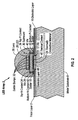
- an LED array 2 includes a plurality of LEDs (e.g., LED 4 ) and a metal substrate 6 .
- a layer 8 of conventional conductive electrical traces is disposed on a dielectric layer 10 overlying metal substrate 6 .
- a plurality of vias (e.g., via 12 ) pass through trace layer 8 and dielectric layer 10 to terminate on or in metal substrate 6 .
- Each of the LEDs is disposed over a corresponding via.
- LED 4 may be any suitable conventional light emitting diode.
- LED 4 may be an AlInGaN LED disclosed in U.S. Pat. No. 6,133,589 or an AlInGaN LED disclosed in U.S. patent application Ser. No. 09/469,657, both of which are assigned to the assignee of the present invention and incorporated herein by reference in their entirety.
- LED 4 is a high flux AlInGaN or AlInGaP LED driven, for example, by a current greater than about 70 milliamps (mA).
- Such high flux LEDs are commercially available from, for example, LumiLeds Lighting U.S., LLC of San Jose, Calif.
- LED 4 includes conventional N-contact 14 and conventional P-contact 16 .
- LED 4 is mounted as a “flip chip” with N-contact 14 and P-contact 16 disposed on the same side of the LED die and oriented to face trace layer 8 .
- N-contact 14 and P-contact 16 are electrically connected to separate ones of the conductive traces in trace layer 8 with conventional reflowed solder 18 .
- LED 4 also includes thermal contact 20 (e.g., a metal pad) disposed on the same side of LED 4 as contacts 14 and 16 .
- thermal contact 20 is electrically isolated from contacts 14 and 16 . Such electrical isolation may be provided, for example, by optional dielectric layer 22 . Other means of electrically isolating thermal contact 20 from contacts 14 and 16 may also be used.
- Electrical contacts 14 and 16 and thermal contact 20 may be conventionally formed, for example, from suitable conventional solderable metal layers.
- Via 12 contains a thermally conductive material 24 in thermal contact with metal substrate 6 and in thermal contact with LED 4 .
- Thermally conductive material 24 forms part of a continuous solid material heat flow path between LED 4 and metal substrate 6 uninterrupted by, for example, liquid or gas filled gaps.
- thermally conductive material 24 is in direct contact with thermal contact 20 of LED 4 and in direct contact with metal substrate 6 . In other embodiments, however, thermal contact may be established without such direct physical contact between thermally conductive material 24 and LED 4 or metal substrate 6 .
- thermally conductive material 24 is or includes a conventional reflowed solder deposited in via 12 by conventional means such as, for example, screen printing.
- thermally conductive material 24 may be the same material as used for reflowed solder 18 , and conductive material 24 and solder 18 may be deposited in the same process step and reflowed in the same process step.
- thermally conductive material 24 includes diamond filled epoxy, silver filled epoxy, or other conventional materials having high adhesion strength and good thermal conductivity.
- thermally conductive material 24 may include metals conventionally plated into via 12 . Such plated metals may fill via 12 to, for example, about the level of trace layer 8 .
- thermally conductive material 24 is electrically conductive, it may be electrically isolated from trace layer 8 and LED 4 by dielectric layer 10 and optional dielectric layer 22 . If thermally conductive material 24 is a reflowable solder material, the thickness of thermally conductive material 24 between metal substrate 6 and thermal contact 20 is, for example, about 0.0002 inches to about 0.005 inches, typically about 0.001 inches.
- Metal substrate 6 is, for example, a copper plate having a thickness greater than about 0.01 inches optionally plated with a solderable material such as nickel or tin to provide good mechanical and thermal contact with thermally conductive material 24 .
- Metal substrate 6 may also be formed from other metals or combinations of metals, and may include two or more metal layers.
- trace layer 8 is formed from an etched and plated copper sheet attached to metal substrate 6 with a conventional dielectric adhesive, such as an epoxy, from which dielectric layer 10 is formed.
- Vias e.g., via 12
- trace layer 8 and dielectric layer 10 may be formed in trace layer 8 and dielectric layer 10 with conventional machine tools, plasma or chemical etching, or by laser ablation, for example.
- LED array 2 may also include lenses (e.g., lens 26 ) disposed over some or all of the LEDs to collect and direct light emitted by the LEDs.
- lenses may be conventionally cast or molded in clear plastic or elastomer onto some or all of the LEDs.
- small portions of silicone or similar clear material may be conventionally dispensed onto some or all of the LEDs and then cured to form simple lenses, or hollow clear lenses may be conventionally heat staked, glued, or press fit over some or all of the LEDs and then filled with silicone, for example, to encapsulate the LEDs.
- Thermal contact 20 and thermally conductive material 24 provide an advantageously low thermal resistance path for heat to flow from LED 4 to metal substrate 6 , which then spreads the heat effectively.
- the thermal resistance of this path is lower than that of thermal paths in, for example, conventional LED arrays formed on conventional printed circuit boards.
- This low resistance thermal path allows the LEDs in array 2 to be operated at higher than conventional current (and thus provide higher than conventional flux) without raising their temperatures to levels that degrade their performance.
- the effective dissipation of heat by thermally conductive material 24 and metal substrate 6 also allows high flux LEDs to be arranged in LED array 2 with a spacing between LEDs less than that in conventional arrays of high flux LEDs without overheating the LEDs and degrading their performance.
- LED array 2 may provide a flux per unit area greater than that in conventional LED arrays.
- wire bonds also improves the reliability of LED array 2 in this embodiment, as wire bonds are typically the least reliable elements of LED arrays.
- each of the LEDs in LED array 2 (e.g., LED 28 ) is attached to a separate submount (e.g., submount 30 ).
- the submounts may be formed, for example, from silicon or ceramic materials.
- Conventional reflowed solder (e.g., Sn/Pb) bumps 32 electrically connect an N-type region of LED 28 to a top N-contact 34 on submount 30 and electrically connect a P-type region of LED 28 to a top P-contact 36 on submount 30 .
- Vias 38 and 40 in submount 30 each contains a conventional electrically conductive material (e.g., tungsten and/or copper) which carries current from, respectively, top N-contact 34 and top P-contact 36 to, respectively, bottom N-contact 42 and bottom P-contact 44 .
- N-contact 42 and P-contact 44 are electrically connected to separate ones of the traces in trace layer 8 with conventional reflowed solder 18 .
- vias 38 and 40 may include a conventionally deposited dielectric tube or liner to prevent shorting of the vias through the submount.
- Submount 30 also includes thermal contact 46 (e.g., a metal pad) disposed on the bottom side of submount 30 adjacent to electrical contacts 42 and 44 .
- thermal contact 46 is electrically isolated from contacts 42 and 44 . Such electrical isolation may be provided, for example, by optional dielectric layer 48 . Other means of electrically isolating thermal contact 46 from contacts 42 and 44 may also be used. Electrical contacts 34 , 36 , 42 , and 44 and thermal contact 46 may be conventionally formed, for example, from suitable conventional solderable metal layers.
- thermally conductive material 24 in via 12 is in direct contact with thermal contact 46 on submount 30 and in thermal contact with LED 28 through submount 30 and solder bumps 32 .
- a reflowed solder used in thermally conductive material 24 has a lower reflow temperature than a reflowed solder used in solder bumps 32 , allowing submount 30 to be attached to metal substrate 6 without disturbing the solder connections between LED 28 and submount 30 .
- submount 30 is thin and formed from a thermally conductive material in order to reduce the thermal resistance provided by submount 30 to the flow of heat from LED 28 to metal substrate 6 .
- a submount formed from silicon typically has a thickness less than about 0.010 inches.
- solder bumps 32 , submount 30 , thermal contact 46 , and thermally conductive material 24 provides a low thermal resistance path for heat to flow from LED 28 to metal substrate 6 .
- This low thermal resistance path provides advantages similar to those of the previous embodiment.
- LEDs mounted on submounts may be pre-tested prior to installation in LED array 2 . Such pre-testing allows the LEDs in LED array 2 to be selected based on well-characterized values for emission wavelength and flux, for example.
- the submounts may include additional circuitry such as electrostatic discharge protection circuitry, for example, which may be advantageous for LED array 2 .
- vias 38 and 40 are absent and N-contact 34 and P-contact 36 on submount 30 are electrically connected to separate ones of the traces in trace layer 8 by, respectively, wire bonds 48 and 50 .
- Wire bonds 48 and 50 may be less expensive to produce than electrical connections through vias.
- trace layer 8 and dielectric layer 10 are included in a thin conventional printed circuit board or flex circuit 52 attached to metal substrate 6 with a conventional dielectric adhesive layer 54 .
- An additional dielectric layer 56 may overlie trace layer 8 .
- Vias may be formed in printed circuit board 52 by punching, for example.
- FIG. 5 schematically illustrates the arrangement of electrical and thermal contacts on the bottom side of an LED assembly 58 included in an LED array in accordance with one embodiment of the present invention.
- LED assembly 58 may include, for example, an LED without a submount such as LED 4 (FIG. 1) or an LED attached to a submount such as LED 28 attached to submount 30 (FIGS. 2, 3 , 4 ).
- N-contact 60 may be, for example, N-contact 14 of LED 4 or bottom N-contact 42 of submount 30 .
- P-contact 62 may be, for example, P-contact 16 of LED 4 or bottom P-contact 44 of submount 30 .
- Thermal contact 64 may be, for example, thermal contact 20 of LED 4 or thermal contact 46 of submount 30 . Thermal contact 64 typically occupies a large fraction of the bottom surface of LED assembly 58 in order to promote the flow of heat through thermal contact 64 to metal substrate 6 .
- FIG. 6 schematically illustrates in a top view an LED array 2 in accordance with one embodiment of the present invention prior to installation of LED assemblies (LEDs with or without submounts) at a plurality of locations 66 - 1 - 66 - 9 .
- a via e.g., via 12
- conductive traces 8 - 1 - 8 - 18 in trace layer 8
- are exposed to make electrical contact with separate ones of the electrical contacts on the bottom side of an LED assembly such as electrical contacts 60 and 62 of LED assembly 58 (FIG. 5 ).
- Conductive electrical traces 8 - 1 - 8 - 18 may be interconnected to put some or all of the LEDs in series, in parallel, or in anti-parallel.
- Through-holes such as through-hole 68 pass through metal substrate 6 and the dielectric and trace layers overlying metal substrate 6 to allow lenses such as lens 26 (FIG. 1) to be filled with an encapsulant such as silicone, for example.
- FIG. 7 schematically illustrates in a top view the LED array 2 of FIG. 6 after attachment of LED assemblies 58 - 1 - 58 - 9 to metal substrate 6 and to conductive traces 8 - 1 - 8 - 16 .
- Each LED assembly is in thermal contact with metal substrate 6 through a thermally conductive material 24 (FIGS. 1-4) deposited in a via located below the LED assembly.
- LED array 2 includes 9 LED assemblies (LEDs with or without submounts). Other embodiments include more or fewer than nine such LED assemblies.
- LEDs 4 and 28 shown in FIGS. 1-4 are flip chips
- the present invention may employ LEDs having one or more electrical contacts on a top side of the LED. Such contacts may be wire bonded, for example, to electrical contacts on a submount or to conductive traces in a trace layer overlying the metal substrate.
- FIGS. 2-4 show only one LED attached to each submount, some embodiments may employ more than one LED per submount. In such embodiments some or all of the multiple LEDs on a submount may be electrically connected, for example, in series, in parallel, or in anti-parallel.
- an LED array in accordance with the present invention may include some LEDs disposed on submounts and some LEDs attached directly to the metal substrate.
- FIGS. 1-4 show only one layer 8 of conductive traces disposed above metal substrate 6 , other embodiments may employ multiple layers of conductive traces.
Abstract
Description
Claims (25)
Priority Applications (4)
| Application Number | Priority Date | Filing Date | Title |
|---|---|---|---|
| US09/974,563 US6498355B1 (en) | 2001-10-09 | 2001-10-09 | High flux LED array |
| TW091123138A TW561635B (en) | 2001-10-09 | 2002-10-07 | High flux LED array |
| DE10246892.3A DE10246892B4 (en) | 2001-10-09 | 2002-10-08 | LED matrix with high radiation power |
| JP2002295370A JP4330863B2 (en) | 2001-10-09 | 2002-10-08 | High bundle LED array |
Applications Claiming Priority (1)
| Application Number | Priority Date | Filing Date | Title |
|---|---|---|---|
| US09/974,563 US6498355B1 (en) | 2001-10-09 | 2001-10-09 | High flux LED array |
Publications (1)
| Publication Number | Publication Date |
|---|---|
| US6498355B1 true US6498355B1 (en) | 2002-12-24 |
Family
ID=25522181
Family Applications (1)
| Application Number | Title | Priority Date | Filing Date |
|---|---|---|---|
| US09/974,563 Expired - Lifetime US6498355B1 (en) | 2001-10-09 | 2001-10-09 | High flux LED array |
Country Status (4)
| Country | Link |
|---|---|
| US (1) | US6498355B1 (en) |
| JP (1) | JP4330863B2 (en) |
| DE (1) | DE10246892B4 (en) |
| TW (1) | TW561635B (en) |
Cited By (287)
| Publication number | Priority date | Publication date | Assignee | Title |
|---|---|---|---|---|
| US20030107885A1 (en) * | 2001-12-10 | 2003-06-12 | Galli Robert D. | LED lighting assembly |
| US20030189201A1 (en) * | 2002-03-04 | 2003-10-09 | United Epitaxy Co., Ltd. | Package of lightemitting diode with protective element |
| US20040026708A1 (en) * | 2002-08-09 | 2004-02-12 | United Epitaxy Co., Ltd. | Sub-mount for high power light emitting diode |
| US20040075399A1 (en) * | 2002-10-22 | 2004-04-22 | Hall David Charles | LED light engine for AC operation and methods of fabricating same |
| US20040135159A1 (en) * | 2003-01-09 | 2004-07-15 | Siegel Stephen B. | Light emitting apparatus and method for curing inks, coatings and adhesives |
| US20040140543A1 (en) * | 2003-01-16 | 2004-07-22 | Elpedes Cresente S. | Accurate alignment of an LED assembly |
| US20040160173A1 (en) * | 2003-02-19 | 2004-08-19 | Yu-Chen Shen | High-powered light emitting device with improved thermal properties |
| US20040164325A1 (en) * | 2003-01-09 | 2004-08-26 | Con-Trol-Cure, Inc. | UV curing for ink jet printer |
| US20040166249A1 (en) * | 2003-01-09 | 2004-08-26 | Con-Trol-Cure, Inc. | UV curing method and apparatus |
| US20040169451A1 (en) * | 2003-02-28 | 2004-09-02 | Citizen Electronics Co., Ltd. | Light emitting element and light emitting device with the light emitting element and method for manufacturing the light emitting element |
| WO2004100265A2 (en) * | 2003-05-08 | 2004-11-18 | Koninklijke Philips Electronics N.V. | Light-emitting diode system |
| US20040238111A1 (en) * | 2003-01-09 | 2004-12-02 | Con-Trol-Cure, Inc. | UV LED control loop and controller for UV curing |
| WO2004105142A1 (en) * | 2003-05-26 | 2004-12-02 | Matsushita Electric Works, Ltd. | Light-emitting device |
| US20040257007A1 (en) * | 1997-12-17 | 2004-12-23 | Color Kinetics, Incorporated | Geometric panel lighting apparatus and methods |
| US20050017366A1 (en) * | 2001-12-10 | 2005-01-27 | Galli Robert D. | LED lighting assembly with improved heat management |
| US20050017256A1 (en) * | 2001-07-23 | 2005-01-27 | Slater David B. | Flip-chip bonding of light emitting devices |
| US20050024864A1 (en) * | 2002-12-10 | 2005-02-03 | Galli Robert D. | Flashlight housing |
| US20050042390A1 (en) * | 2003-01-09 | 2005-02-24 | Siegel Stephen B. | Rotary UV curing method and apparatus |
| EP1511090A2 (en) * | 2003-08-29 | 2005-03-02 | LumiLeds Lighting U.S., LLC | Package for a semiconductor light emitting device |
| US20050051789A1 (en) * | 2003-09-09 | 2005-03-10 | Negley Gerald H. | Solid metal block mounting substrates for semiconductor light emitting devices, and oxidizing methods for fabricating same |
| US20050104946A1 (en) * | 2003-01-09 | 2005-05-19 | Con-Trol-Cure, Inc. | Ink jet UV curing |
| US20050110395A1 (en) * | 2003-10-24 | 2005-05-26 | Seiko Epson Corporation | Light source apparatus and projector |
| WO2005048358A1 (en) | 2003-11-07 | 2005-05-26 | Tridonic Optoelectronics Gmbh | Light-emitting diode arrangement comprising a heat-dissipating plate |
| US20050116667A1 (en) * | 2001-09-17 | 2005-06-02 | Color Kinetics, Incorporated | Tile lighting methods and systems |
| JP2005158957A (en) * | 2003-11-25 | 2005-06-16 | Matsushita Electric Works Ltd | Light emitting device |
| US20050161692A1 (en) * | 2001-12-10 | 2005-07-28 | Galli Robert D. | Led lighting assembly |
| US20050168990A1 (en) * | 2004-01-13 | 2005-08-04 | Seiko Epson Corporation | Light source apparatus and projection display apparatus |
| US20050179049A1 (en) * | 2004-02-13 | 2005-08-18 | Ying-Ming Ho | Light emitting diode |
| US20050199899A1 (en) * | 2004-03-11 | 2005-09-15 | Ming-Der Lin | Package array and package unit of flip chip LED |
| US20050207166A1 (en) * | 2004-01-28 | 2005-09-22 | Peter Kan | Directly viewable luminaire |
| US20050222295A1 (en) * | 2003-01-09 | 2005-10-06 | Con-Trol-Cure, Inc. | UV Curing System and Process with Increased Light Intensity |
| US20050230600A1 (en) * | 2004-03-30 | 2005-10-20 | Olson Steven J | LED array having array-based LED detectors |
| US20050239227A1 (en) * | 2002-08-30 | 2005-10-27 | Gelcore, Llc | Light emitting diode component |
| EP1598591A2 (en) * | 2003-12-05 | 2005-11-23 | Welwyn Components Limited | Light emitting assembly |
| EP1605525A2 (en) * | 2004-06-10 | 2005-12-14 | LG Electronics Inc. | High power LED package |
| US20050276052A1 (en) * | 2002-12-16 | 2005-12-15 | Junichi Shimada | Led illumination system |
| US20060002125A1 (en) * | 2004-07-01 | 2006-01-05 | Samsung Electro-Mechanics Co., Ltd. | Light emitting diode module for automobile headlights and automobile headlight having the same |
| US20060006405A1 (en) * | 2003-05-05 | 2006-01-12 | Lamina Ceramics, Inc. | Surface mountable light emitting diode assemblies packaged for high temperature operation |
| US20060006524A1 (en) * | 2004-07-07 | 2006-01-12 | Min-Hsun Hsieh | Light emitting diode having an adhesive layer formed with heat paths |
| US20060012299A1 (en) * | 2003-07-17 | 2006-01-19 | Yoshinobu Suehiro | Light emitting device |
| US20060013014A1 (en) * | 2004-07-02 | 2006-01-19 | Robert Hayman | Dental light devices having an improved heat sink |
| US20060018123A1 (en) * | 2004-07-02 | 2006-01-26 | Rose Eric P | Curing light having a reflector |
| US20060023432A1 (en) * | 2004-07-30 | 2006-02-02 | Patent-Treuhand-Gesellschaft Fur Elektrische Gluhlampen Mbh | Printed circuit board and method for producing such a printed circuit board |
| US20060024638A1 (en) * | 2004-07-02 | 2006-02-02 | Kenneth Rosenblood | Curing light |
| WO2006013503A2 (en) * | 2004-07-27 | 2006-02-09 | Koninklijke Philips Electronics N.V. | Light emitting diode assembly |
| WO2006023300A2 (en) * | 2004-08-18 | 2006-03-02 | Cree, Inc. | Methods of assembly for a semiconductor light emitting device package |
| DE102004045950A1 (en) * | 2004-09-22 | 2006-03-30 | Osram Opto Semiconductors Gmbh | Housing for an optoelectronic component, optoelectronic component and method for producing an optoelectronic component |
| US20060071329A1 (en) * | 2004-09-24 | 2006-04-06 | Du Shawn X | Power led package |
| WO2006038543A2 (en) | 2004-10-04 | 2006-04-13 | Toshiba Kk | Light emitting device, lighting equipment or liquid crystal display device using such light emitting device |
| US20060097245A1 (en) * | 2002-08-30 | 2006-05-11 | Aanegola Srinath K | Light emitting diode component |
| US20060121208A1 (en) * | 2003-01-09 | 2006-06-08 | Siegel Stephen B | Multiple wavelength UV curing |
| US20060131601A1 (en) * | 2004-12-21 | 2006-06-22 | Ouderkirk Andrew J | Illumination assembly and method of making same |
| US20060131602A1 (en) * | 2004-12-21 | 2006-06-22 | Ouderkirk Andrew J | Illumination assembly and method of making same |
| US20060131596A1 (en) * | 2004-12-21 | 2006-06-22 | Ouderkirk Andrew J | Illumination assembly and method of making same |
| US20060138621A1 (en) * | 2002-09-30 | 2006-06-29 | Osram Opto Semiconductors Gmbh | Optoelectronic component and a module based thereon |
| US20060139945A1 (en) * | 2004-12-23 | 2006-06-29 | Negley Gerald H | Light emitting diode arrays for direct backlighting of liquid crystal displays |
| US20060145180A1 (en) * | 2001-12-10 | 2006-07-06 | Galli Robert D | Led lighting assembly |
| US20060154393A1 (en) * | 2005-01-11 | 2006-07-13 | Doan Trung T | Systems and methods for removing operating heat from a light emitting diode |
| US20060152651A1 (en) * | 2005-01-12 | 2006-07-13 | Negley Gerald H | Solid colloidal dispersions for backlighting of liquid crystal displays |
| US20060151801A1 (en) * | 2005-01-11 | 2006-07-13 | Doan Trung T | Light emitting diode with thermo-electric cooler |
| US20060186423A1 (en) * | 2003-05-05 | 2006-08-24 | Greg Blonder | Method of making optical light engines with elevated LEDs and resulting product |
| US20060192222A1 (en) * | 2004-12-08 | 2006-08-31 | Jyh-Chen Chen | Light emitting device |
| US20060208271A1 (en) * | 2005-03-21 | 2006-09-21 | Lg Electronics Inc. | Light source apparatus and fabrication method thereof |
| WO2006101257A1 (en) * | 2005-03-23 | 2006-09-28 | Matsushita Electric Industrial Co., Ltd. | Light-emitting module |
| US20060216865A1 (en) * | 2004-03-18 | 2006-09-28 | Phoseon Technology, Inc. | Direct cooling of leds |
| US20060261470A1 (en) * | 2005-04-05 | 2006-11-23 | Tir Systems Ltd. | Electronic device package with an integrated evaporator |
| US20060278885A1 (en) * | 2005-06-14 | 2006-12-14 | Industrial Technology Research Institute | LED wafer-level chip scale packaging |
| US20060286697A1 (en) * | 2005-06-16 | 2006-12-21 | Leem See J | Method for manufacturing light emitting diodes |
| US20060289887A1 (en) * | 2005-06-24 | 2006-12-28 | Jabil Circuit, Inc. | Surface mount light emitting diode (LED) assembly with improved power dissipation |
| WO2007000037A1 (en) * | 2005-06-29 | 2007-01-04 | Mitchell, Richard, J. | Bendable high flux led array |
| US20070001564A1 (en) * | 2005-06-30 | 2007-01-04 | Lg.Philips Lcd Co., Ltd. | Light emitting diode package in backlight unit for liquid crystal display device |
| US20070018175A1 (en) * | 2003-05-05 | 2007-01-25 | Joseph Mazzochette | Light emitting diodes with improved light collimation |
| US20070044357A1 (en) * | 2004-03-15 | 2007-03-01 | Onscreen Technologies, Inc. | Rapid Dispatch Emergency Signs |
| US20070051964A1 (en) * | 2004-04-12 | 2007-03-08 | Owen Mark D | High density led array |
| US7201492B2 (en) | 2001-12-10 | 2007-04-10 | Robert Galli | LED lighting assembly |
| US20070081339A1 (en) * | 2005-10-07 | 2007-04-12 | Chung Huai-Ku | LED light source module with high efficiency heat dissipation |
| US20070086188A1 (en) * | 2004-05-18 | 2007-04-19 | Onscreen Technologies, Inc. | LED Assembly with Vented Circuit Board |
| US20070111351A1 (en) * | 2003-07-11 | 2007-05-17 | Tridonic Optoelectronics Gmbh | Led and led light source |
| EP1791187A1 (en) * | 2005-11-29 | 2007-05-30 | National Central University | Light emitting device |
| US20070176182A1 (en) * | 2006-01-27 | 2007-08-02 | Way-Jze Wen | Structure for integrating LED circuit onto heat-dissipation substrate |
| US20070189042A1 (en) * | 2006-02-08 | 2007-08-16 | Chi Mei Optoelectronics Corporation | Flat panel display having backlight module |
| US20070194709A1 (en) * | 2003-01-10 | 2007-08-23 | Toyoda Gosei Co., Ltd. | Light emitting device |
| US20070291503A1 (en) * | 2004-02-26 | 2007-12-20 | Marco Friedrich | Light-Emitting Diode Arrangement for a High-Power Ligth-Emitting Diode and Method for Producing a Light-Emitting Diode Arrangement |
| US20080012506A1 (en) * | 1997-08-26 | 2008-01-17 | Color Kinetics Incorporated | Multicolored led lighting method and apparatus |
| KR100796670B1 (en) | 2006-04-27 | 2008-01-22 | (주)루멘스 | Light Emitting Diode and Method for manufacturing thereof |
| EP1883120A2 (en) * | 2006-07-28 | 2008-01-30 | Gia Tzoong Enterprise Co. Ltd. | LED substrate |
| US20080036045A1 (en) * | 2006-08-08 | 2008-02-14 | Silicon Base Development Inc. | Package-base structure of power semiconductor device and manufacturing process of the same |
| US20080042867A1 (en) * | 2006-08-21 | 2008-02-21 | Swantner Michael J | Illuminable indicator and light engine therefor |
| US20080054280A1 (en) * | 2006-09-06 | 2008-03-06 | Gelcore Llc | Light emitting packages and methods of making same |
| CN100375300C (en) * | 2003-11-25 | 2008-03-12 | 葛世潮 | High power LED |
| US20080062715A1 (en) * | 2006-09-08 | 2008-03-13 | Samsung Electronics Co., Ltd. | Backlight assembly and liquid crystal display having the same |
| US20080061314A1 (en) * | 2006-09-13 | 2008-03-13 | Tsung-Jen Liaw | Light emitting device with high heat-dissipating capability |
| US20080068807A1 (en) * | 2006-09-20 | 2008-03-20 | Sunonwealth Electric Machine Industry Co., Ltd. | Heat-dissipating device for back light source for flat panel display |
| DE202006017583U1 (en) * | 2006-11-17 | 2008-03-27 | Patent-Treuhand-Gesellschaft für elektrische Glühlampen mbH | lighting device |
| DE102006059702A1 (en) * | 2006-09-29 | 2008-04-03 | Osram Opto Semiconductors Gmbh | Opto-electronic element has metal core plate, metal core, dielectric layer applied on metal core and electrically conductive layer applied on dielectric layer and element also has chip carrier connected with metal core plate |
| US20080101073A1 (en) * | 2006-11-01 | 2008-05-01 | Discus Dental, Llc | Dental Light Devices Having an Improved Heat Sink |
| CN100388513C (en) * | 2003-05-14 | 2008-05-14 | 纳米封装工艺公司 | Light emitting device, package structure thereof and manufacturing method thereof |
| US20080111470A1 (en) * | 2006-11-09 | 2008-05-15 | Thomas Cheng-Hsin Yuan | Expandable LED array interconnect |
| CN100391017C (en) * | 2003-05-26 | 2008-05-28 | 松下电工株式会社 | Light-emitting device |
| US20080123334A1 (en) * | 2006-11-03 | 2008-05-29 | Hochstein Peter A | LED light engine with applied foil construction |
| EP1928029A1 (en) * | 2005-09-20 | 2008-06-04 | Matsushita Electric Works, Ltd. | Light emitting device |
| US20080169480A1 (en) * | 2007-01-11 | 2008-07-17 | Visera Technologies Company Limited | Optoelectronic device package and packaging method thereof |
| US20080180960A1 (en) * | 2006-10-31 | 2008-07-31 | Shane Harrah | Lighting device package |
| EP1953834A1 (en) * | 2005-11-21 | 2008-08-06 | Matsushita Electric Works, Ltd. | Light-emitting device |
| WO2008104103A1 (en) * | 2007-03-01 | 2008-09-04 | Tsungwen Chan | Method for manufacturing a plurality of smd leds and structure thereof |
| CN100420019C (en) * | 2005-04-20 | 2008-09-17 | 王锐勋 | Packaging method for colony light-emitting diode chips and devices thereof |
| US20080254649A1 (en) * | 2007-04-10 | 2008-10-16 | Raled, Inc. | Thermal management of leds on a printed circuit board and associated methods |
| US20080278954A1 (en) * | 2005-04-05 | 2008-11-13 | Tir Systems Ltd. | Mounting Assembly for Optoelectronic Devices |
| US20080296589A1 (en) * | 2005-03-24 | 2008-12-04 | Ingo Speier | Solid-State Lighting Device Package |
| US20080296599A1 (en) * | 2005-06-27 | 2008-12-04 | Mazzochette Joseph B | LED Package with Stepped Aperture |
| US20090008662A1 (en) * | 2007-07-05 | 2009-01-08 | Ian Ashdown | Lighting device package |
| US20090015134A1 (en) * | 2007-07-13 | 2009-01-15 | Kai-Yu Lin | Heat dissipation arrangement of a light emitting module |
| US20090026485A1 (en) * | 2005-06-30 | 2009-01-29 | Matsushita Electric Works, Ltd. | Light-emitting device |
| US7498065B2 (en) | 2003-01-09 | 2009-03-03 | Con-Trol-Cure, Inc. | UV printing and curing of CDs, DVDs, Golf Balls And Other Products |
| US20090086438A1 (en) * | 2007-09-27 | 2009-04-02 | Beijing Boe Optoelectronics Technology Co., Ltd. | Led element and printed circuit board with the same |
| US20090086491A1 (en) * | 2007-09-28 | 2009-04-02 | Ruud Lighting, Inc. | Aerodynamic LED Floodlight Fixture |
| US20090095967A1 (en) * | 2005-11-21 | 2009-04-16 | Mikio Masui | Light emitting device |
| US7524085B2 (en) | 2003-10-31 | 2009-04-28 | Phoseon Technology, Inc. | Series wiring of highly reliable light sources |
| US20090129076A1 (en) * | 2007-11-19 | 2009-05-21 | Osram Gesellschaft Mit Beschrankter Haftung | Illumination device comprising a heat sink |
| US20090135567A1 (en) * | 2007-11-23 | 2009-05-28 | Industrial Technology Research Institute | Metal thermal interface material and thermal module and packaged microelectronic component containing the material |
| GB2455069A (en) * | 2007-11-16 | 2009-06-03 | Uriel Meyer Wittenberg | LED cooling arrangement |
| US7543956B2 (en) | 2005-02-28 | 2009-06-09 | Philips Solid-State Lighting Solutions, Inc. | Configurations and methods for embedding electronics or light emitters in manufactured materials |
| US20090208894A1 (en) * | 2008-02-18 | 2009-08-20 | Discus Dental, Llc | Curing Light |
| US20090231849A1 (en) * | 2008-03-12 | 2009-09-17 | Bright Led Electronics Corp. | Light emitting diode lighting module and method for making the same |
| US7618163B2 (en) | 2007-04-02 | 2009-11-17 | Ruud Lighting, Inc. | Light-directing LED apparatus |
| US20090284932A1 (en) * | 2008-03-25 | 2009-11-19 | Bridge Semiconductor Corporation | Thermally Enhanced Package with Embedded Metal Slug and Patterned Circuitry |
| US7638808B2 (en) | 2004-03-18 | 2009-12-29 | Phoseon Technology, Inc. | Micro-reflectors on a substrate for high-density LED array |
| US7642527B2 (en) | 2005-12-30 | 2010-01-05 | Phoseon Technology, Inc. | Multi-attribute light effects for use in curing and other applications involving photoreactions and processing |
| US20100001309A1 (en) * | 2008-03-25 | 2010-01-07 | Bridge Semiconductor Corporation | Semiconductor chip assembly with post/base heat spreader and horizontal signal routing |
| US20100006867A1 (en) * | 2006-09-30 | 2010-01-14 | Seoul Opto Device Co., Ltd. | Light emitting diode having light emitting cell with different size and light emitting device thereof |
| US7659674B2 (en) | 1997-08-26 | 2010-02-09 | Philips Solid-State Lighting Solutions, Inc. | Wireless lighting control methods and apparatus |
| US7671346B2 (en) | 2003-01-09 | 2010-03-02 | Con-Trol-Cure, Inc. | Light emitting apparatus and method for curing inks, coatings and adhesives |
| US20100052005A1 (en) * | 2008-03-25 | 2010-03-04 | Lin Charles W C | Semiconductor chip assembly with post/base heat spreader and conductive trace |
| US20100066236A1 (en) * | 2008-09-12 | 2010-03-18 | Bridgelux, Inc. | Method and Apparatus for Generating Phosphor Film with Textured Surface |
| US20100075448A1 (en) * | 2008-03-25 | 2010-03-25 | Bridge Semiconductor Corporation | Method of making a semiconductor chip assembly with a post/base/cap heat spreader |
| US20100072511A1 (en) * | 2008-03-25 | 2010-03-25 | Lin Charles W C | Semiconductor chip assembly with copper/aluminum post/base heat spreader |
| US7686469B2 (en) | 2006-09-30 | 2010-03-30 | Ruud Lighting, Inc. | LED lighting fixture |
| EP1544924A3 (en) * | 2003-12-19 | 2010-03-31 | Philips Lumileds Lighting Company LLC | LED package assembly |
| US20100096662A1 (en) * | 2008-03-25 | 2010-04-22 | Bridge Semiconductor Corporation | Semiconductor chip assembly with post/base heat spreader and signal post |
| US20100102354A1 (en) * | 2008-10-23 | 2010-04-29 | Everlight Electronics Co., Ltd. | Light emitting diode package |
| USD615504S1 (en) * | 2007-10-31 | 2010-05-11 | Cree, Inc. | Emitter package |
| US20100148196A1 (en) * | 2005-09-20 | 2010-06-17 | Matsushita Electric Works, Ltd. | Led lighting fixture |
| US20100148208A1 (en) * | 2002-12-10 | 2010-06-17 | Galli Robert D | Led lighting assembly with improved heat management |
| US20100155751A1 (en) * | 2007-05-09 | 2010-06-24 | Foxsemicon Integrated Technology, Inc. | Light emitting diode assembly and light emitting diode display device |
| US20100155769A1 (en) * | 2008-03-25 | 2010-06-24 | Bridge Semiconductor Corporation | Semiconductor chip assembly with base heat spreader and cavity in base |
| US20100155768A1 (en) * | 2008-03-25 | 2010-06-24 | Bridge Semiconductor Corporation | Semiconductor chip assembly with post/base heat spreader and cavity in post |
| US20100163921A1 (en) * | 2008-03-25 | 2010-07-01 | Bridge Semiconductor Corporation | Semiconductor chip assembly with aluminum post/base heat spreader and silver/copper conductive trace |
| US20100181890A1 (en) * | 2009-01-17 | 2010-07-22 | Bright Led Electronics Corp. | Lighting device and method for making the same |
| US20100181594A1 (en) * | 2008-03-25 | 2010-07-22 | Lin Charles W C | Semiconductor chip assembly with post/base heat spreader and cavity over post |
| US20100237369A1 (en) * | 2009-03-17 | 2010-09-23 | Toyoda Gosei Co., Ltd. | Light-emitting device |
| US20100243230A1 (en) * | 2009-03-25 | 2010-09-30 | Wah Hong Industrial Corp. | Heat-dissipating device including a plating metal layer |
| US7819550B2 (en) | 2003-10-31 | 2010-10-26 | Phoseon Technology, Inc. | Collection optics for led array with offset hemispherical or faceted surfaces |
| US20100289054A1 (en) * | 2008-03-25 | 2010-11-18 | Bridge Semiconductor Corporation | Semiconductor chip assembly with post/base heat spreader and adhesive between base and terminal |
| US7841750B2 (en) | 2008-08-01 | 2010-11-30 | Ruud Lighting, Inc. | Light-directing lensing member with improved angled light distribution |
| US20100302789A1 (en) * | 2009-05-28 | 2010-12-02 | Qing Li | LED Light Source Module and Method for Producing the Same |
| WO2010140875A1 (en) * | 2009-06-05 | 2010-12-09 | Alfredo Villafranca Quinto | Light fitting for the exterior environment and public highways with leds as lighting element |
| US20100322785A1 (en) * | 2008-02-25 | 2010-12-23 | Marcel Buse | Compressor Unit |
| US20100327310A1 (en) * | 2008-03-25 | 2010-12-30 | Lin Charles W C | Semiconductor chip assembly with post/base/flange heat spreader and cavity in flange |
| WO2011008278A1 (en) * | 2009-07-16 | 2011-01-20 | Prism Projection, Inc. | Solid state light fixture |
| US20110039374A1 (en) * | 2008-03-25 | 2011-02-17 | Bridge Semiconductor Corporation | Method of making a semiconductor chip assembly with a bump/base heat spreader and a cavity in the bump |
| WO2011018689A1 (en) * | 2009-08-13 | 2011-02-17 | SemiLEDs Optoelectronics Co., Ltd. | Smart integrated semiconductor light emitting system including light emitting diodes and application specific integrated circuits (asic) |
| US20110049558A1 (en) * | 2008-03-25 | 2011-03-03 | Lin Charles W C | Semiconductor chip assembly with post/base heat spreader, signal post and cavity |
| US7906793B2 (en) | 2004-10-25 | 2011-03-15 | Cree, Inc. | Solid metal block semiconductor light emitting device mounting substrates |
| US7906794B2 (en) | 2006-07-05 | 2011-03-15 | Koninklijke Philips Electronics N.V. | Light emitting device package with frame and optically transmissive element |
| US20110065241A1 (en) * | 2008-03-25 | 2011-03-17 | Bridge Semiconductor Corporation | Method of making a semiconductor chip assembly with a bump/base heat spreader and a dual-angle cavity in the bump |
| WO2011037655A1 (en) * | 2009-09-24 | 2011-03-31 | Molex Incorporated | Light module system |
| US20110089465A1 (en) * | 2008-03-25 | 2011-04-21 | Lin Charles W C | Semiconductor chip assembly with post/base heat spreader with esd protection layer |
| US20110095325A1 (en) * | 2005-01-18 | 2011-04-28 | Epistar Corporation | Optoelectronic semiconductor device and manufacturing method thereof |
| US20110101410A1 (en) * | 2008-03-25 | 2011-05-05 | Lin Charles W C | Semiconductor chip assembly with post/base/post heat spreader |
| US20110104855A1 (en) * | 2008-03-25 | 2011-05-05 | Bridge Semiconductor Corporation | Method of making a semiconductor chip assembly with a post/base heat spreader with an ESD protection layer |
| US7952262B2 (en) | 2006-09-30 | 2011-05-31 | Ruud Lighting, Inc. | Modular LED unit incorporating interconnected heat sinks configured to mount and hold adjacent LED modules |
| US20110140150A1 (en) * | 2009-09-11 | 2011-06-16 | Soraa, Inc. | System and Method for LED Packaging |
| US20110151626A1 (en) * | 2008-03-25 | 2011-06-23 | Lin Charles W C | Method of making a semiconductor chip assembly with a post/base/post heat spreader and asymmetric posts |
| US20110163348A1 (en) * | 2008-03-25 | 2011-07-07 | Bridge Semiconductor Corporation | Semiconductor chip assembly with bump/base heat spreader and inverted cavity in bump |
| US20110183472A1 (en) * | 2008-03-25 | 2011-07-28 | Bridge Semiconductor Corporation | Method of making a semiconductor chip assembly with a post/base heat spreader and a plated through-hole |
| US20110186873A1 (en) * | 2009-06-05 | 2011-08-04 | Emerson David T | Light emitting device packages, systems and methods |
| US20110201157A1 (en) * | 2008-03-25 | 2011-08-18 | Bridge Semiconductor Corporation. | Method of making a semiconductor chip assembly with a post/base heat spreader and a multilevel conductive trace |
| US20110214851A1 (en) * | 2009-08-14 | 2011-09-08 | Wah Hong Industrial Corp. | Use of a graphite heat-dissipation device including a plating metal layer |
| US20110227122A1 (en) * | 2008-03-25 | 2011-09-22 | Bridge Semiconductor Corporation | Semiconductor chip assembly with post/base heat spreader with thermal via |
| US8033692B2 (en) | 2006-05-23 | 2011-10-11 | Cree, Inc. | Lighting device |
| US20110273904A1 (en) * | 2010-05-06 | 2011-11-10 | Funai Electric Co., Ltd. | Light source structure |
| US20110279981A1 (en) * | 2010-05-17 | 2011-11-17 | Alex Horng | Heat Dissipating Assembly |
| US8077305B2 (en) | 2004-04-19 | 2011-12-13 | Owen Mark D | Imaging semiconductor structures using solid state illumination |
| EP2398072A1 (en) * | 2009-02-10 | 2011-12-21 | Nichia Corporation | Semiconductor light-emitting device |
| CN102299080A (en) * | 2011-08-29 | 2011-12-28 | 深南电路有限公司 | Substrate and processing method thereof |
| CN101594730B (en) * | 2008-05-26 | 2012-01-04 | 欣兴电子股份有限公司 | Circuit board with conductive structure |
| DE102010033093A1 (en) * | 2010-08-02 | 2012-02-02 | Osram Opto Semiconductors Gmbh | Optoelectronic light module and vehicle headlamp |
| US8153477B2 (en) | 2008-03-25 | 2012-04-10 | Bridge Semiconductor Corporation | Method of making a semiconductor chip assembly with a post/dielectric/post heat spreader |
| FR2966286A1 (en) * | 2010-10-14 | 2012-04-20 | Sgame | Unitary or elementary components for receiving power LEDs of e.g. lighting tube, has specific printed circuit whose thickness corresponds to thickness of standard printed circuit for receiving other components |
| US8192053B2 (en) | 2002-05-08 | 2012-06-05 | Phoseon Technology, Inc. | High efficiency solid-state light source and methods of use and manufacture |
| CN102569278A (en) * | 2010-10-26 | 2012-07-11 | 东芝照明技术株式会社 | Light emitting device and illumination device |
| US8232576B1 (en) | 2008-03-25 | 2012-07-31 | Bridge Semiconductor Corporation | Semiconductor chip assembly with post/base heat spreader and ceramic block in post |
| CN102637804A (en) * | 2012-04-23 | 2012-08-15 | 木林森股份有限公司 | Inversion structure for bonding-free LED (Light Emitting Diode) chip |
| US8293551B2 (en) | 2010-06-18 | 2012-10-23 | Soraa, Inc. | Gallium and nitrogen containing triangular or diamond-shaped configuration for optical devices |
| US8304292B1 (en) | 2009-08-06 | 2012-11-06 | Bridge Semiconductor Corporation | Method of making a semiconductor chip assembly with a ceramic/metal substrate |
| US8314408B2 (en) | 2008-12-31 | 2012-11-20 | Draka Comteq, B.V. | UVLED apparatus for curing glass-fiber coatings |
| CN102790161A (en) * | 2011-05-18 | 2012-11-21 | 台湾积体电路制造股份有限公司 | Light emitting diode carrier |
| US8348475B2 (en) | 2008-05-23 | 2013-01-08 | Ruud Lighting, Inc. | Lens with controlled backlight management |
| US20130011946A1 (en) * | 2010-06-28 | 2013-01-10 | Cree, Inc. | Led package with efficient, isolated thermal path |
| US8354688B2 (en) | 2008-03-25 | 2013-01-15 | Bridge Semiconductor Corporation | Semiconductor chip assembly with bump/base/ledge heat spreader, dual adhesives and cavity in bump |
| EP2339900A3 (en) * | 2009-12-22 | 2013-01-23 | Automotive Lighting Reutlingen GmbH | Light module for a lighting device of a motor vehicle and lighting device with such a light module |
| US8388193B2 (en) | 2008-05-23 | 2013-03-05 | Ruud Lighting, Inc. | Lens with TIR for off-axial light distribution |
| US8502465B2 (en) | 2009-09-18 | 2013-08-06 | Soraa, Inc. | Power light emitting diode and method with current density operation |
| US8511851B2 (en) | 2009-12-21 | 2013-08-20 | Cree, Inc. | High CRI adjustable color temperature lighting devices |
| US20130229800A1 (en) * | 2004-12-17 | 2013-09-05 | Lg Innotek Co., Ltd. | Package for light emitting device and method for packaging the same |
| US8541951B1 (en) | 2010-11-17 | 2013-09-24 | Soraa, Inc. | High temperature LED system using an AC power source |
| EP2645436A1 (en) * | 2012-03-28 | 2013-10-02 | Commissariat à l'Énergie Atomique et aux Énergies Alternatives | LED component with low thermal resistance having separate electrical and thermal pathways |
| WO2013149772A1 (en) * | 2012-04-02 | 2013-10-10 | Osram Opto Semiconductors Gmbh | Light-emitting semiconductor component and method for producing a light-emitting semiconductor component |
| US20130271992A1 (en) * | 2010-11-02 | 2013-10-17 | Shinwoo Tech Co., Ltd. | Led array module and manufacturing method thereof |
| US8575642B1 (en) | 2009-10-30 | 2013-11-05 | Soraa, Inc. | Optical devices having reflection mode wavelength material |
| US8618560B2 (en) | 2009-04-07 | 2013-12-31 | Soraa, Inc. | Polarized white light devices using non-polar or semipolar gallium containing materials and transparent phosphors |
| USD697664S1 (en) | 2012-05-07 | 2014-01-14 | Cree, Inc. | LED lens |
| US8648359B2 (en) | 2010-06-28 | 2014-02-11 | Cree, Inc. | Light emitting devices and methods |
| USD700584S1 (en) | 2011-07-06 | 2014-03-04 | Cree, Inc. | LED component |
| US8686431B2 (en) | 2011-08-22 | 2014-04-01 | Soraa, Inc. | Gallium and nitrogen containing trilateral configuration for optical devices |
| US8686445B1 (en) | 2009-06-05 | 2014-04-01 | Cree, Inc. | Solid state lighting devices and methods |
| USD704358S1 (en) | 2011-01-03 | 2014-05-06 | Cree, Inc. | High brightness LED package |
| US8740413B1 (en) | 2010-02-03 | 2014-06-03 | Soraa, Inc. | System and method for providing color light sources in proximity to predetermined wavelength conversion structures |
| USD708156S1 (en) | 2010-07-16 | 2014-07-01 | Cree, Inc. | Package for light emitting diode (LED) lighting |
| US8772817B2 (en) | 2010-12-22 | 2014-07-08 | Cree, Inc. | Electronic device submounts including substrates with thermally conductive vias |
| US8786053B2 (en) | 2011-01-24 | 2014-07-22 | Soraa, Inc. | Gallium-nitride-on-handle substrate materials and devices and method of manufacture |
| US8783915B2 (en) | 2010-02-11 | 2014-07-22 | Bridgelux, Inc. | Surface-textured encapsulations for use with light emitting diodes |
| WO2014111384A1 (en) * | 2013-01-17 | 2014-07-24 | Osram Opto Semiconductors Gmbh | Optoelectronic semiconductor chip |
| US8791499B1 (en) | 2009-05-27 | 2014-07-29 | Soraa, Inc. | GaN containing optical devices and method with ESD stability |
| US8802471B1 (en) | 2012-12-21 | 2014-08-12 | Soraa, Inc. | Contacts for an n-type gallium and nitrogen substrate for optical devices |
| US8858004B2 (en) | 2005-12-22 | 2014-10-14 | Cree, Inc. | Lighting device |
| US8866166B2 (en) | 2009-06-05 | 2014-10-21 | Cree, Inc. | Solid state lighting device |
| US8871311B2 (en) | 2010-06-03 | 2014-10-28 | Draka Comteq, B.V. | Curing method employing UV sources that emit differing ranges of UV radiation |
| US8896235B1 (en) | 2010-11-17 | 2014-11-25 | Soraa, Inc. | High temperature LED system using an AC power source |
| USD718490S1 (en) | 2013-03-15 | 2014-11-25 | Cree, Inc. | LED lens |
| US8905588B2 (en) | 2010-02-03 | 2014-12-09 | Sorra, Inc. | System and method for providing color light sources in proximity to predetermined wavelength conversion structures |
| US8912025B2 (en) | 2011-11-23 | 2014-12-16 | Soraa, Inc. | Method for manufacture of bright GaN LEDs using a selective removal process |
| US20140375212A1 (en) * | 2013-06-21 | 2014-12-25 | Micron Technology, Inc. | Multi-junction solid state transducer devices for direct ac power and associated systems and methods |
| US8926145B2 (en) | 2008-12-05 | 2015-01-06 | Permlight Products, Inc. | LED-based light engine having thermally insulated zones |
| US20150028376A1 (en) * | 2013-07-23 | 2015-01-29 | Grote Industries, Llc | Flexible lighting device having unobtrusive conductive layers |
| US8971368B1 (en) | 2012-08-16 | 2015-03-03 | Soraa Laser Diode, Inc. | Laser devices having a gallium and nitrogen containing semipolar surface orientation |
| US20150061513A1 (en) * | 2013-08-30 | 2015-03-05 | Paragon Semiconductor Lighting Technology Co., Ltd. | Multichip package structure |
| US8974080B2 (en) | 2009-10-12 | 2015-03-10 | Molex Incorporated | Light module |
| US8985794B1 (en) | 2012-04-17 | 2015-03-24 | Soraa, Inc. | Providing remote blue phosphors in an LED lamp |
| US8994033B2 (en) | 2013-07-09 | 2015-03-31 | Soraa, Inc. | Contacts for an n-type gallium and nitrogen substrate for optical devices |
| US9000466B1 (en) | 2010-08-23 | 2015-04-07 | Soraa, Inc. | Methods and devices for light extraction from a group III-nitride volumetric LED using surface and sidewall roughening |
| US9028087B2 (en) | 2006-09-30 | 2015-05-12 | Cree, Inc. | LED light fixture |
| US9046227B2 (en) | 2009-09-18 | 2015-06-02 | Soraa, Inc. | LED lamps with improved quality of light |
| US9105806B2 (en) | 2009-03-09 | 2015-08-11 | Soraa, Inc. | Polarization direction of optical devices using selected spatial configurations |
| US9111778B2 (en) | 2009-06-05 | 2015-08-18 | Cree, Inc. | Light emitting diode (LED) devices, systems, and methods |
| US9123874B2 (en) | 2009-01-12 | 2015-09-01 | Cree, Inc. | Light emitting device packages with improved heat transfer |
| US9187367B2 (en) | 2010-05-20 | 2015-11-17 | Draka Comteq, B.V. | Curing apparatus employing angled UVLEDs |
| WO2016004341A1 (en) * | 2014-07-03 | 2016-01-07 | Sansi Technology, Inc. | Lighting device and led luminaire incorporating the same. |
| US9243794B2 (en) | 2006-09-30 | 2016-01-26 | Cree, Inc. | LED light fixture with fluid flow to and from the heat sink |
| US9255686B2 (en) | 2009-05-29 | 2016-02-09 | Cree, Inc. | Multi-lens LED-array optic system |
| US9269876B2 (en) | 2012-03-06 | 2016-02-23 | Soraa, Inc. | Light emitting diodes with low refractive index material layers to reduce light guiding effects |
| US9281001B2 (en) | 2004-11-08 | 2016-03-08 | Phoseon Technology, Inc. | Methods and systems relating to light sources for use in industrial processes |
| US9293644B2 (en) | 2009-09-18 | 2016-03-22 | Soraa, Inc. | Power light emitting diode and method with uniform current density operation |
| US9293667B2 (en) | 2010-08-19 | 2016-03-22 | Soraa, Inc. | System and method for selected pump LEDs with multiple phosphors |
| US9303861B2 (en) | 2009-09-14 | 2016-04-05 | Us Vaopto, Inc. | Light emitting diode light source modules |
| US20160100479A1 (en) * | 2014-10-06 | 2016-04-07 | E.G.O. Elektro-Geraetebau Gmbh | Display device |
| US9335006B2 (en) | 2006-04-18 | 2016-05-10 | Cree, Inc. | Saturated yellow phosphor converted LED and blue converted red LED |
| US9419189B1 (en) | 2013-11-04 | 2016-08-16 | Soraa, Inc. | Small LED source with high brightness and high efficiency |
| US9423096B2 (en) | 2008-05-23 | 2016-08-23 | Cree, Inc. | LED lighting apparatus |
| US9450143B2 (en) | 2010-06-18 | 2016-09-20 | Soraa, Inc. | Gallium and nitrogen containing triangular or diamond-shaped configuration for optical devices |
| US9488324B2 (en) | 2011-09-02 | 2016-11-08 | Soraa, Inc. | Accessories for LED lamp systems |
| US9523479B2 (en) | 2014-01-03 | 2016-12-20 | Cree, Inc. | LED lens |
| US9541258B2 (en) | 2012-02-29 | 2017-01-10 | Cree, Inc. | Lens for wide lateral-angle distribution |
| US9541257B2 (en) | 2012-02-29 | 2017-01-10 | Cree, Inc. | Lens for primarily-elongate light distribution |
| US9583678B2 (en) | 2009-09-18 | 2017-02-28 | Soraa, Inc. | High-performance LED fabrication |
| US9648750B2 (en) | 2014-09-30 | 2017-05-09 | Rsm Electron Power, Inc. | Light emitting diode (LED) assembly and flexible circuit board with improved thermal conductivity |
| US9761763B2 (en) | 2012-12-21 | 2017-09-12 | Soraa, Inc. | Dense-luminescent-materials-coated violet LEDs |
| US9786811B2 (en) | 2011-02-04 | 2017-10-10 | Cree, Inc. | Tilted emission LED array |
| US9841175B2 (en) | 2012-05-04 | 2017-12-12 | GE Lighting Solutions, LLC | Optics system for solid state lighting apparatus |
| US9859471B2 (en) | 2011-01-31 | 2018-01-02 | Cree, Inc. | High brightness light emitting diode (LED) packages, systems and methods with improved resin filling and high adhesion |
| US9951938B2 (en) | 2009-10-02 | 2018-04-24 | GE Lighting Solutions, LLC | LED lamp |
| US9978904B2 (en) | 2012-10-16 | 2018-05-22 | Soraa, Inc. | Indium gallium nitride light emitting devices |
| US10029942B2 (en) | 2010-08-10 | 2018-07-24 | Draka Comteq B.V. | Method and apparatus providing increased UVLED intensity and uniform curing of optical-fiber coatings |
| US10147850B1 (en) | 2010-02-03 | 2018-12-04 | Soraa, Inc. | System and method for providing color light sources in proximity to predetermined wavelength conversion structures |
| US20190162372A1 (en) * | 2016-05-13 | 2019-05-30 | Rohinni, LLC | Light Vectoring Apparatus |
| US10408429B2 (en) | 2012-02-29 | 2019-09-10 | Ideal Industries Lighting Llc | Lens for preferential-side distribution |
| US20190333903A1 (en) * | 2017-10-20 | 2019-10-31 | Facebook Technologies, Llc | Elastomeric layer fabrication for light emitting diodes |
| US10468566B2 (en) | 2017-04-10 | 2019-11-05 | Ideal Industries Lighting Llc | Hybrid lens for controlled light distribution |
| US10516084B2 (en) | 2014-10-31 | 2019-12-24 | eLux, Inc. | Encapsulated fluid assembly emissive elements |
| CN111148353A (en) * | 2019-12-30 | 2020-05-12 | 乐健科技(珠海)有限公司 | Preparation method of circuit board with copper-based heat sink |
| US10842016B2 (en) | 2011-07-06 | 2020-11-17 | Cree, Inc. | Compact optically efficient solid state light source with integrated thermal management |
| US11032976B1 (en) | 2020-03-16 | 2021-06-15 | Hgci, Inc. | Light fixture for indoor grow application and components thereof |
| US11101408B2 (en) | 2011-02-07 | 2021-08-24 | Creeled, Inc. | Components and methods for light emitting diode (LED) lighting |
| USD933872S1 (en) | 2020-03-16 | 2021-10-19 | Hgci, Inc. | Light fixture |
| USD933881S1 (en) | 2020-03-16 | 2021-10-19 | Hgci, Inc. | Light fixture having heat sink |
| US11380828B2 (en) * | 2017-10-26 | 2022-07-05 | Epistar Corporation | Light-emitting device |
| US20230003372A1 (en) * | 2021-07-04 | 2023-01-05 | Ming-Teng KUO | Light source module |
Families Citing this family (23)
| Publication number | Priority date | Publication date | Assignee | Title |
|---|---|---|---|---|
| JP2006525682A (en) | 2003-04-30 | 2006-11-09 | クリー インコーポレイテッド | High power solid state light emitting device package |
| US7005679B2 (en) | 2003-05-01 | 2006-02-28 | Cree, Inc. | Multiple component solid state white light |
| WO2004102685A1 (en) * | 2003-05-14 | 2004-11-25 | Nano Packaging Technology, Inc. | Light emitting device, package structure thereof and manufacturing method thereof |
| JP4712293B2 (en) * | 2003-10-01 | 2011-06-29 | 株式会社半導体エネルギー研究所 | projector |
| JP5349755B2 (en) * | 2003-12-09 | 2013-11-20 | ジーイー ライティング ソリューションズ エルエルシー | Surface mount light emitting chip package |
| DE102004016847A1 (en) | 2004-04-07 | 2005-12-22 | P.M.C. Projekt Management Consult Gmbh | Light emitting diode arrangement and method for producing a light emitting diode array |
| US7534633B2 (en) | 2004-07-02 | 2009-05-19 | Cree, Inc. | LED with substrate modifications for enhanced light extraction and method of making same |
| KR101197046B1 (en) | 2005-01-26 | 2012-11-06 | 삼성디스플레이 주식회사 | Two dimensional light source of using light emitting diode and liquid crystal display panel of using the two dimensional light source |
| JP5237540B2 (en) * | 2005-09-20 | 2013-07-17 | パナソニック株式会社 | Light emitting device |
| JP5155540B2 (en) * | 2005-09-20 | 2013-03-06 | パナソニック株式会社 | Light emitting device |
| JP5237539B2 (en) * | 2005-09-20 | 2013-07-17 | パナソニック株式会社 | Light emitting device |
| JP2007234886A (en) * | 2006-03-01 | 2007-09-13 | Compal Communications Inc | Electronic element assembly with thermal dissipation constitution |
| CN102437152A (en) | 2006-04-24 | 2012-05-02 | 克利公司 | Side-view surface mount white LED |
| JP5149601B2 (en) * | 2007-11-27 | 2013-02-20 | パナソニック株式会社 | Light emitting device |
| US9431589B2 (en) | 2007-12-14 | 2016-08-30 | Cree, Inc. | Textured encapsulant surface in LED packages |
| DE102008022414B4 (en) * | 2008-05-06 | 2013-03-14 | Rüdiger Lanz | Illuminants for use in street lighting and a device for street lighting |
| DE102009034082A1 (en) | 2009-07-21 | 2011-01-27 | Osram Gesellschaft mit beschränkter Haftung | Optoelectronic assembly and method for producing such a unit |
| KR100962706B1 (en) * | 2009-11-27 | 2010-06-15 | 주식회사 테크엔 | Manufacture method of the large illuminations with power led |
| US8455895B2 (en) * | 2010-11-08 | 2013-06-04 | Bridgelux, Inc. | LED-based light source utilizing asymmetric conductors |
| KR101995538B1 (en) * | 2012-09-28 | 2019-07-02 | 제너럴 일렉트릭 캄파니 | Overlay circuit structure for interconnecting light emitting semiconductors |
| CN104241262B (en) | 2013-06-14 | 2020-11-06 | 惠州科锐半导体照明有限公司 | Light emitting device and display device |
| FR3025859A1 (en) * | 2014-09-15 | 2016-03-18 | Valeo Vision | LUMINOUS MODULE SUBSTRATE WITH METALLIC TRACK FOR SHIELDING, THERMAL SCREEN AND / OR OPTICAL REFLECTOR |
| KR102085649B1 (en) * | 2019-06-26 | 2020-03-06 | 제너럴 일렉트릭 캄파니 | Overlay circuit structure for interconnecting light emitting semiconductors |
Citations (2)
| Publication number | Priority date | Publication date | Assignee | Title |
|---|---|---|---|---|
| US6045240A (en) * | 1996-06-27 | 2000-04-04 | Relume Corporation | LED lamp assembly with means to conduct heat away from the LEDS |
| US6133589A (en) | 1999-06-08 | 2000-10-17 | Lumileds Lighting, U.S., Llc | AlGaInN-based LED having thick epitaxial layer for improved light extraction |
Family Cites Families (1)
| Publication number | Priority date | Publication date | Assignee | Title |
|---|---|---|---|---|
| US6428189B1 (en) * | 2000-03-31 | 2002-08-06 | Relume Corporation | L.E.D. thermal management |
-
2001
- 2001-10-09 US US09/974,563 patent/US6498355B1/en not_active Expired - Lifetime
-
2002
- 2002-10-07 TW TW091123138A patent/TW561635B/en not_active IP Right Cessation
- 2002-10-08 JP JP2002295370A patent/JP4330863B2/en not_active Expired - Lifetime
- 2002-10-08 DE DE10246892.3A patent/DE10246892B4/en not_active Expired - Lifetime
Patent Citations (2)
| Publication number | Priority date | Publication date | Assignee | Title |
|---|---|---|---|---|
| US6045240A (en) * | 1996-06-27 | 2000-04-04 | Relume Corporation | LED lamp assembly with means to conduct heat away from the LEDS |
| US6133589A (en) | 1999-06-08 | 2000-10-17 | Lumileds Lighting, U.S., Llc | AlGaInN-based LED having thick epitaxial layer for improved light extraction |
Cited By (558)
| Publication number | Priority date | Publication date | Assignee | Title |
|---|---|---|---|---|
| US7659674B2 (en) | 1997-08-26 | 2010-02-09 | Philips Solid-State Lighting Solutions, Inc. | Wireless lighting control methods and apparatus |
| US20080012506A1 (en) * | 1997-08-26 | 2008-01-17 | Color Kinetics Incorporated | Multicolored led lighting method and apparatus |
| US20040257007A1 (en) * | 1997-12-17 | 2004-12-23 | Color Kinetics, Incorporated | Geometric panel lighting apparatus and methods |
| US7180252B2 (en) | 1997-12-17 | 2007-02-20 | Color Kinetics Incorporated | Geometric panel lighting apparatus and methods |
| US7259033B2 (en) | 2001-07-23 | 2007-08-21 | Cree, Inc. | Flip-chip bonding of light emitting devices |
| US20050017256A1 (en) * | 2001-07-23 | 2005-01-27 | Slater David B. | Flip-chip bonding of light emitting devices |
| US7608860B2 (en) | 2001-07-23 | 2009-10-27 | Cree, Inc. | Light emitting devices suitable for flip-chip bonding |
| US6888167B2 (en) | 2001-07-23 | 2005-05-03 | Cree, Inc. | Flip-chip bonding of light emitting devices and light emitting devices suitable for flip-chip bonding |
| US20070241360A1 (en) * | 2001-07-23 | 2007-10-18 | Cree, Inc. | Light emitting devices suitable for flip-chip bonding |
| US7358929B2 (en) | 2001-09-17 | 2008-04-15 | Philips Solid-State Lighting Solutions, Inc. | Tile lighting methods and systems |
| US20050116667A1 (en) * | 2001-09-17 | 2005-06-02 | Color Kinetics, Incorporated | Tile lighting methods and systems |
| US7121680B2 (en) | 2001-12-10 | 2006-10-17 | Galli Robert D | LED lighting assembly with improved heat management |
| US20030107885A1 (en) * | 2001-12-10 | 2003-06-12 | Galli Robert D. | LED lighting assembly |
| US20050161692A1 (en) * | 2001-12-10 | 2005-07-28 | Galli Robert D. | Led lighting assembly |
| US20060145180A1 (en) * | 2001-12-10 | 2006-07-06 | Galli Robert D | Led lighting assembly |
| US7201492B2 (en) | 2001-12-10 | 2007-04-10 | Robert Galli | LED lighting assembly |
| US6827468B2 (en) * | 2001-12-10 | 2004-12-07 | Robert D. Galli | LED lighting assembly |
| US7652303B2 (en) | 2001-12-10 | 2010-01-26 | Galli Robert D | LED lighting assembly |
| US20050017366A1 (en) * | 2001-12-10 | 2005-01-27 | Galli Robert D. | LED lighting assembly with improved heat management |
| US7118255B2 (en) | 2001-12-10 | 2006-10-10 | Galli Robert D | LED lighting assembly with improved heat exchange |
| US6861677B2 (en) * | 2002-03-04 | 2005-03-01 | United Epitaxy Co., Ltd. | Package of lightemitting diode with protective element |
| US20030189201A1 (en) * | 2002-03-04 | 2003-10-09 | United Epitaxy Co., Ltd. | Package of lightemitting diode with protective element |
| US8496356B2 (en) | 2002-05-08 | 2013-07-30 | Phoseon Technology, Inc. | High efficiency solid-state light source and methods of use and manufacture |
| US8192053B2 (en) | 2002-05-08 | 2012-06-05 | Phoseon Technology, Inc. | High efficiency solid-state light source and methods of use and manufacture |
| US10401012B2 (en) | 2002-05-08 | 2019-09-03 | Phoseon Technology, Inc. | High efficiency solid-state light source and methods of use and manufacture |
| US20040026708A1 (en) * | 2002-08-09 | 2004-02-12 | United Epitaxy Co., Ltd. | Sub-mount for high power light emitting diode |
| US7800121B2 (en) | 2002-08-30 | 2010-09-21 | Lumination Llc | Light emitting diode component |
| US20050239227A1 (en) * | 2002-08-30 | 2005-10-27 | Gelcore, Llc | Light emitting diode component |
| US20110001422A1 (en) * | 2002-08-30 | 2011-01-06 | Lumination Llc | Light emitting diode component |
| US8436380B2 (en) | 2002-08-30 | 2013-05-07 | GE Lighting Solutions, LLC | Light emitting diode component |
| US8362695B2 (en) | 2002-08-30 | 2013-01-29 | GE Lighting Solutions, LLC | Light emitting diode component |
| US20060097245A1 (en) * | 2002-08-30 | 2006-05-11 | Aanegola Srinath K | Light emitting diode component |
| US7224000B2 (en) * | 2002-08-30 | 2007-05-29 | Lumination, Llc | Light emitting diode component |
| US20060138621A1 (en) * | 2002-09-30 | 2006-06-29 | Osram Opto Semiconductors Gmbh | Optoelectronic component and a module based thereon |
| US7586190B2 (en) * | 2002-09-30 | 2009-09-08 | Osram Opto Semiconductors Gmbh | Optoelectronic component and a module based thereon |
| WO2004038801A3 (en) * | 2002-10-22 | 2004-10-07 | Cree Inc | Light emitting diode assembly for ac operation and methods of fabricating same |
| US20040075399A1 (en) * | 2002-10-22 | 2004-04-22 | Hall David Charles | LED light engine for AC operation and methods of fabricating same |
| WO2004038801A2 (en) * | 2002-10-22 | 2004-05-06 | Cree, Inc. | Light emitting diode assembly for ac operation and methods of fabricating same |
| US7009199B2 (en) * | 2002-10-22 | 2006-03-07 | Cree, Inc. | Electronic devices having a header and antiparallel connected light emitting diodes for producing light from AC current |
| US20050024864A1 (en) * | 2002-12-10 | 2005-02-03 | Galli Robert D. | Flashlight housing |
| US20100148208A1 (en) * | 2002-12-10 | 2010-06-17 | Galli Robert D | Led lighting assembly with improved heat management |
| US8093620B2 (en) | 2002-12-10 | 2012-01-10 | Galli Robert D | LED lighting assembly with improved heat management |
| US7153004B2 (en) | 2002-12-10 | 2006-12-26 | Galli Robert D | Flashlight housing |
| US7400029B2 (en) * | 2002-12-16 | 2008-07-15 | Yanchers Inc. | LED illumination system |
| US20080259607A1 (en) * | 2002-12-16 | 2008-10-23 | Yanchers Inc. | LED illumination system |
| US20050276052A1 (en) * | 2002-12-16 | 2005-12-15 | Junichi Shimada | Led illumination system |
| US7834434B2 (en) * | 2002-12-16 | 2010-11-16 | Yanchers Inc. | LED illumination system |
| US20050042390A1 (en) * | 2003-01-09 | 2005-02-24 | Siegel Stephen B. | Rotary UV curing method and apparatus |
| US7399982B2 (en) | 2003-01-09 | 2008-07-15 | Con-Trol-Cure, Inc | UV curing system and process with increased light intensity |
| US7175712B2 (en) | 2003-01-09 | 2007-02-13 | Con-Trol-Cure, Inc. | Light emitting apparatus and method for curing inks, coatings and adhesives |
| US20040166249A1 (en) * | 2003-01-09 | 2004-08-26 | Con-Trol-Cure, Inc. | UV curing method and apparatus |
| US20040164325A1 (en) * | 2003-01-09 | 2004-08-26 | Con-Trol-Cure, Inc. | UV curing for ink jet printer |
| US20050104946A1 (en) * | 2003-01-09 | 2005-05-19 | Con-Trol-Cure, Inc. | Ink jet UV curing |
| US7498065B2 (en) | 2003-01-09 | 2009-03-03 | Con-Trol-Cure, Inc. | UV printing and curing of CDs, DVDs, Golf Balls And Other Products |
| US7137696B2 (en) | 2003-01-09 | 2006-11-21 | Con-Trol-Cure, Inc. | Ink jet UV curing |
| US7465909B2 (en) | 2003-01-09 | 2008-12-16 | Con-Trol-Cure, Inc. | UV LED control loop and controller for causing emitting UV light at a much greater intensity for UV curing |
| US7671346B2 (en) | 2003-01-09 | 2010-03-02 | Con-Trol-Cure, Inc. | Light emitting apparatus and method for curing inks, coatings and adhesives |
| US20040238111A1 (en) * | 2003-01-09 | 2004-12-02 | Con-Trol-Cure, Inc. | UV LED control loop and controller for UV curing |
| US20060121208A1 (en) * | 2003-01-09 | 2006-06-08 | Siegel Stephen B | Multiple wavelength UV curing |
| US20050222295A1 (en) * | 2003-01-09 | 2005-10-06 | Con-Trol-Cure, Inc. | UV Curing System and Process with Increased Light Intensity |
| US7211299B2 (en) | 2003-01-09 | 2007-05-01 | Con-Trol-Cure, Inc. | UV curing method and apparatus |
| US20040135159A1 (en) * | 2003-01-09 | 2004-07-15 | Siegel Stephen B. | Light emitting apparatus and method for curing inks, coatings and adhesives |
| US20070194709A1 (en) * | 2003-01-10 | 2007-08-23 | Toyoda Gosei Co., Ltd. | Light emitting device |
| US7550777B2 (en) * | 2003-01-10 | 2009-06-23 | Toyoda Gosei, Co., Ltd. | Light emitting device including adhesion layer |
| US7795051B2 (en) | 2003-01-16 | 2010-09-14 | Philips Lumileds Lighting Company, Llc | Accurate alignment of an LED assembly |
| US20070117273A1 (en) * | 2003-01-16 | 2007-05-24 | Philips Lumileds Lighting Company, Llc | Accurate Alignment of an LED Assembly |
| JP2004221598A (en) * | 2003-01-16 | 2004-08-05 | Lumileds Lighting Us Llc | Accurate alignment for led assembly |
| US20040140543A1 (en) * | 2003-01-16 | 2004-07-22 | Elpedes Cresente S. | Accurate alignment of an LED assembly |
| US7170151B2 (en) * | 2003-01-16 | 2007-01-30 | Philips Lumileds Lighting Company, Llc | Accurate alignment of an LED assembly |
| EP1450417A1 (en) * | 2003-02-19 | 2004-08-25 | LumiLeds Lighting U.S., LLC | High-powered light emitting device with improved thermal properties |
| US6977396B2 (en) | 2003-02-19 | 2005-12-20 | Lumileds Lighting U.S., Llc | High-powered light emitting device with improved thermal properties |
| US7351599B2 (en) | 2003-02-19 | 2008-04-01 | Philips Lumileds Lighting Company Llc | High-powered light emitting device with improved thermal properties |
| US20040160173A1 (en) * | 2003-02-19 | 2004-08-19 | Yu-Chen Shen | High-powered light emitting device with improved thermal properties |
| US20060097336A1 (en) * | 2003-02-19 | 2006-05-11 | Yu-Chen Shen | High-powered light emitting device with improved thermal properties |
| US20040169451A1 (en) * | 2003-02-28 | 2004-09-02 | Citizen Electronics Co., Ltd. | Light emitting element and light emitting device with the light emitting element and method for manufacturing the light emitting element |
| US7253447B2 (en) * | 2003-02-28 | 2007-08-07 | Citizen Electronics Co., Ltd. | Light emitting element and light emitting device with the light emitting element and method for manufacturing the light emitting element |
| DE102004009998B4 (en) * | 2003-02-28 | 2010-05-06 | Citizen Electronics Co., Ltd., Fujiyoshida-shi | A light emitting diode and light emitting diode device comprising a light emitting diode |
| US7528421B2 (en) | 2003-05-05 | 2009-05-05 | Lamina Lighting, Inc. | Surface mountable light emitting diode assemblies packaged for high temperature operation |
| US7777235B2 (en) | 2003-05-05 | 2010-08-17 | Lighting Science Group Corporation | Light emitting diodes with improved light collimation |
| US20060186423A1 (en) * | 2003-05-05 | 2006-08-24 | Greg Blonder | Method of making optical light engines with elevated LEDs and resulting product |
| US20060006405A1 (en) * | 2003-05-05 | 2006-01-12 | Lamina Ceramics, Inc. | Surface mountable light emitting diode assemblies packaged for high temperature operation |
| US20070018175A1 (en) * | 2003-05-05 | 2007-01-25 | Joseph Mazzochette | Light emitting diodes with improved light collimation |
| US7633093B2 (en) * | 2003-05-05 | 2009-12-15 | Lighting Science Group Corporation | Method of making optical light engines with elevated LEDs and resulting product |
| WO2004100265A3 (en) * | 2003-05-08 | 2005-06-02 | Koninkl Philips Electronics Nv | Light-emitting diode system |
| WO2004100265A2 (en) * | 2003-05-08 | 2004-11-18 | Koninklijke Philips Electronics N.V. | Light-emitting diode system |
| CN100388513C (en) * | 2003-05-14 | 2008-05-14 | 纳米封装工艺公司 | Light emitting device, package structure thereof and manufacturing method thereof |
| US7495322B2 (en) * | 2003-05-26 | 2009-02-24 | Panasonic Electric Works Co., Ltd. | Light-emitting device |
| CN100391017C (en) * | 2003-05-26 | 2008-05-28 | 松下电工株式会社 | Light-emitting device |
| WO2004105142A1 (en) * | 2003-05-26 | 2004-12-02 | Matsushita Electric Works, Ltd. | Light-emitting device |
| EP2365539A1 (en) * | 2003-05-26 | 2011-09-14 | Panasonic Electric Works Co., Ltd | Light-emitting device |
| US20070007540A1 (en) * | 2003-05-26 | 2007-01-11 | Matsushita Electric Works, Ltd. | Light-emitting device |
| US8614456B2 (en) * | 2003-07-11 | 2013-12-24 | Tridonic Optoelectronics Gmbh | LED and LED light source |
| US20070111351A1 (en) * | 2003-07-11 | 2007-05-17 | Tridonic Optoelectronics Gmbh | Led and led light source |
| DE102004063978B4 (en) | 2003-07-17 | 2019-01-24 | Toyoda Gosei Co., Ltd. | Light-emitting device |
| US7391153B2 (en) | 2003-07-17 | 2008-06-24 | Toyoda Gosei Co., Ltd. | Light emitting device provided with a submount assembly for improved thermal dissipation |
| US20060012299A1 (en) * | 2003-07-17 | 2006-01-19 | Yoshinobu Suehiro | Light emitting device |
| EP1511090A2 (en) * | 2003-08-29 | 2005-03-02 | LumiLeds Lighting U.S., LLC | Package for a semiconductor light emitting device |
| US7759144B2 (en) | 2003-08-29 | 2010-07-20 | Philips Lumileds Lighting Company Llc | Package for a semiconductor light emitting device |
| US20090170226A1 (en) * | 2003-08-29 | 2009-07-02 | Philips Lumileds Lighting Company, Llc | Package for a Semiconductor Light Emitting Device |
| EP1511090A3 (en) * | 2003-08-29 | 2009-12-09 | Philips Lumileds Lighting Company LLC | Package for a semiconductor light emitting device |
| US20050051789A1 (en) * | 2003-09-09 | 2005-03-10 | Negley Gerald H. | Solid metal block mounting substrates for semiconductor light emitting devices, and oxidizing methods for fabricating same |
| US7183587B2 (en) | 2003-09-09 | 2007-02-27 | Cree, Inc. | Solid metal block mounting substrates for semiconductor light emitting devices |
| US20050110395A1 (en) * | 2003-10-24 | 2005-05-26 | Seiko Epson Corporation | Light source apparatus and projector |
| US7304418B2 (en) * | 2003-10-24 | 2007-12-04 | Seiko Epson Corporation | Light source apparatus with light-emitting chip which generates light and heat |
| US8523387B2 (en) | 2003-10-31 | 2013-09-03 | Phoseon Technology, Inc. | Collection optics for LED array with offset hemispherical or faceted surfaces |
| US7524085B2 (en) | 2003-10-31 | 2009-04-28 | Phoseon Technology, Inc. | Series wiring of highly reliable light sources |
| US7819550B2 (en) | 2003-10-31 | 2010-10-26 | Phoseon Technology, Inc. | Collection optics for led array with offset hemispherical or faceted surfaces |
| AU2004310132B2 (en) * | 2003-11-07 | 2010-04-22 | Ledon Lighting Jennersdorf Gmbh | Light-emitting diode arrangement comprising a heat-dissipating plate |
| CN100442552C (en) * | 2003-11-07 | 2008-12-10 | 特里多尼克光电子有限公司 | Light-emitting diode arrangement comprising a heat-dissipating plate |
| US8766283B2 (en) * | 2003-11-07 | 2014-07-01 | Tridonic Optoelectronics Gmbh | Light-emitting diode arrangement with heat dissipating plate |
| US20070138488A1 (en) * | 2003-11-07 | 2007-06-21 | Tridonic Optoelectronics Gmgh | Light-emitting diode arrangement with heat dissipating plate |
| WO2005048358A1 (en) | 2003-11-07 | 2005-05-26 | Tridonic Optoelectronics Gmbh | Light-emitting diode arrangement comprising a heat-dissipating plate |
| JP2005158957A (en) * | 2003-11-25 | 2005-06-16 | Matsushita Electric Works Ltd | Light emitting device |
| CN100375300C (en) * | 2003-11-25 | 2008-03-12 | 葛世潮 | High power LED |
| EP1598591A2 (en) * | 2003-12-05 | 2005-11-23 | Welwyn Components Limited | Light emitting assembly |
| EP1598591A3 (en) * | 2003-12-05 | 2007-08-01 | Welwyn Components Limited | Light emitting assembly |
| EP1544924A3 (en) * | 2003-12-19 | 2010-03-31 | Philips Lumileds Lighting Company LLC | LED package assembly |
| TWI382559B (en) * | 2003-12-19 | 2013-01-11 | Philips Lumileds Lighting Co | Led package assembly |
| CN100416405C (en) * | 2004-01-13 | 2008-09-03 | 精工爱普生株式会社 | Light source apparatus and projection display apparatus |
| US20050168990A1 (en) * | 2004-01-13 | 2005-08-04 | Seiko Epson Corporation | Light source apparatus and projection display apparatus |
| US7309145B2 (en) | 2004-01-13 | 2007-12-18 | Seiko Epson Corporation | Light source apparatus and projection display apparatus |
| US20050207166A1 (en) * | 2004-01-28 | 2005-09-22 | Peter Kan | Directly viewable luminaire |
| US7267461B2 (en) | 2004-01-28 | 2007-09-11 | Tir Systems, Ltd. | Directly viewable luminaire |
| US7654703B2 (en) | 2004-01-28 | 2010-02-02 | Koninklijke Philips Electronics, N.V. | Directly viewable luminaire |
| US20070274084A1 (en) * | 2004-01-28 | 2007-11-29 | Tir Systems Ltd. | Directly viewable luminaire |
| US20050179049A1 (en) * | 2004-02-13 | 2005-08-18 | Ying-Ming Ho | Light emitting diode |
| US20070291503A1 (en) * | 2004-02-26 | 2007-12-20 | Marco Friedrich | Light-Emitting Diode Arrangement for a High-Power Ligth-Emitting Diode and Method for Producing a Light-Emitting Diode Arrangement |
| US8975532B2 (en) * | 2004-02-26 | 2015-03-10 | OSPAM Opto Semiconductor GmbH | Light-emitting diode arrangement for a high-power light-emitting diode and method for producing a light-emitting diode arrangement |
| US20050199899A1 (en) * | 2004-03-11 | 2005-09-15 | Ming-Der Lin | Package array and package unit of flip chip LED |
| US20070044357A1 (en) * | 2004-03-15 | 2007-03-01 | Onscreen Technologies, Inc. | Rapid Dispatch Emergency Signs |
| US8637332B2 (en) | 2004-03-18 | 2014-01-28 | Phoseon Technology, Inc. | Micro-reflectors on a substrate for high-density LED array |
| US7638808B2 (en) | 2004-03-18 | 2009-12-29 | Phoseon Technology, Inc. | Micro-reflectors on a substrate for high-density LED array |
| US20060216865A1 (en) * | 2004-03-18 | 2006-09-28 | Phoseon Technology, Inc. | Direct cooling of leds |
| US20100052002A1 (en) * | 2004-03-18 | 2010-03-04 | Phoseon Technology, Inc. | Micro-reflectors on a substrate for high-density led array |
| US7285445B2 (en) | 2004-03-18 | 2007-10-23 | Phoseon Technology, Inc. | Direct cooling of LEDs |
| US7235878B2 (en) | 2004-03-18 | 2007-06-26 | Phoseon Technology, Inc. | Direct cooling of LEDs |
| US7816638B2 (en) | 2004-03-30 | 2010-10-19 | Phoseon Technology, Inc. | LED array having array-based LED detectors |
| US20050230600A1 (en) * | 2004-03-30 | 2005-10-20 | Olson Steven J | LED array having array-based LED detectors |
| US20070051964A1 (en) * | 2004-04-12 | 2007-03-08 | Owen Mark D | High density led array |
| US8077305B2 (en) | 2004-04-19 | 2011-12-13 | Owen Mark D | Imaging semiconductor structures using solid state illumination |
| AU2005239406B2 (en) * | 2004-04-26 | 2011-10-06 | Gelcore Llc | Light emitting diode component |
| CN103633228A (en) * | 2004-04-26 | 2014-03-12 | 吉尔科有限公司 | Light emitting package and method for manufacturing light emitting package |
| WO2005106926A3 (en) * | 2004-04-26 | 2006-06-01 | Gelcore Llc | Light emitting diode component |
| US20070086187A1 (en) * | 2004-05-18 | 2007-04-19 | Onscreen Technologies, Inc. | LED Assembly with Vented Circuit Board |
| US20070086188A1 (en) * | 2004-05-18 | 2007-04-19 | Onscreen Technologies, Inc. | LED Assembly with Vented Circuit Board |
| US20050274959A1 (en) * | 2004-06-10 | 2005-12-15 | Geun-Ho Kim | High power LED package |
| EP1605525A2 (en) * | 2004-06-10 | 2005-12-14 | LG Electronics Inc. | High power LED package |
| EP1605525A3 (en) * | 2004-06-10 | 2006-10-04 | LG Electronics Inc. | High power LED package |
| US20060002125A1 (en) * | 2004-07-01 | 2006-01-05 | Samsung Electro-Mechanics Co., Ltd. | Light emitting diode module for automobile headlights and automobile headlight having the same |
| US7128454B2 (en) * | 2004-07-01 | 2006-10-31 | Samsung Electro-Mechanics Co., Ltd. | Light emitting diode module for automobile headlights and automobile headlight having the same |
| US7273369B2 (en) | 2004-07-02 | 2007-09-25 | Discus Dental, Llc | Curing light |
| US7581846B2 (en) | 2004-07-02 | 2009-09-01 | Discus Dental, Llc | Dental light devices having an improved heat sink |
| US20060040231A1 (en) * | 2004-07-02 | 2006-02-23 | Discus Dental Impressions, Inc. | Curing light capable of multiple wavelengths |
| US20060024638A1 (en) * | 2004-07-02 | 2006-02-02 | Kenneth Rosenblood | Curing light |
| US20060018123A1 (en) * | 2004-07-02 | 2006-01-26 | Rose Eric P | Curing light having a reflector |
| US20060013014A1 (en) * | 2004-07-02 | 2006-01-19 | Robert Hayman | Dental light devices having an improved heat sink |
| US20060006524A1 (en) * | 2004-07-07 | 2006-01-12 | Min-Hsun Hsieh | Light emitting diode having an adhesive layer formed with heat paths |
| US20080290354A1 (en) * | 2004-07-27 | 2008-11-27 | Koninklijke Philips Electronics, N.V. | Light Emitting Diode Assembly |
| WO2006013503A2 (en) * | 2004-07-27 | 2006-02-09 | Koninklijke Philips Electronics N.V. | Light emitting diode assembly |
| WO2006013503A3 (en) * | 2004-07-27 | 2006-07-06 | Koninkl Philips Electronics Nv | Light emitting diode assembly |
| US20060023432A1 (en) * | 2004-07-30 | 2006-02-02 | Patent-Treuhand-Gesellschaft Fur Elektrische Gluhlampen Mbh | Printed circuit board and method for producing such a printed circuit board |
| US7405093B2 (en) * | 2004-08-18 | 2008-07-29 | Cree, Inc. | Methods of assembly for a semiconductor light emitting device package |
| WO2006023300A2 (en) * | 2004-08-18 | 2006-03-02 | Cree, Inc. | Methods of assembly for a semiconductor light emitting device package |
| US20060063287A1 (en) * | 2004-08-18 | 2006-03-23 | Peter Andrews | Methods of assembly for a semiconductor light emitting device package |
| TWI385817B (en) * | 2004-08-18 | 2013-02-11 | Cree Inc | Methods of assembly for a semiconductor light emitting device package |
| WO2006023300A3 (en) * | 2004-08-18 | 2006-11-02 | Cree Inc | Methods of assembly for a semiconductor light emitting device package |
| US20080265266A1 (en) * | 2004-09-22 | 2008-10-30 | Osram Opto Semiconductors Gmbh | Housing for an Optoelectronic Component, Optoelectronic Component and Method for the Production of an Optoelectronic Component |
| US8227821B2 (en) * | 2004-09-22 | 2012-07-24 | Osram Opto Semiconductors Gmbh | Housing for an optoelectronic component, optoelectronic component and method for the production of an optoelectronic component |
| DE102004045950A1 (en) * | 2004-09-22 | 2006-03-30 | Osram Opto Semiconductors Gmbh | Housing for an optoelectronic component, optoelectronic component and method for producing an optoelectronic component |
| US7081667B2 (en) | 2004-09-24 | 2006-07-25 | Gelcore, Llc | Power LED package |
| US20060071329A1 (en) * | 2004-09-24 | 2006-04-06 | Du Shawn X | Power led package |
| WO2006038543A2 (en) | 2004-10-04 | 2006-04-13 | Toshiba Kk | Light emitting device, lighting equipment or liquid crystal display device using such light emitting device |
| EP1806789A4 (en) * | 2004-10-04 | 2009-09-02 | Toshiba Kk | Light emitting device, lighting equipment or liquid crystal display device using such light emitting device |
| US7812360B2 (en) | 2004-10-04 | 2010-10-12 | Kabushiki Kaisha Toshiba | Light emitting device, lighting equipment or liquid crystal display device using such light emitting device |
| US20070247855A1 (en) * | 2004-10-04 | 2007-10-25 | Kabushiki Kaisha Toshiba | Light Emitting Device,Lighting Equipment or Liquid Crystal Display Device Using Such Light Emitting Device |
| EP1806789A2 (en) * | 2004-10-04 | 2007-07-11 | Kabushiki Kaisha Toshiba | Light emitting device, lighting equipment or liquid crystal display device using such light emitting device |
| US7906793B2 (en) | 2004-10-25 | 2011-03-15 | Cree, Inc. | Solid metal block semiconductor light emitting device mounting substrates |
| US8598606B2 (en) | 2004-10-25 | 2013-12-03 | Cree, Inc. | Solid metal block semiconductor light emitting device mounting substrates and packages |
| US9281001B2 (en) | 2004-11-08 | 2016-03-08 | Phoseon Technology, Inc. | Methods and systems relating to light sources for use in industrial processes |
| US20060192222A1 (en) * | 2004-12-08 | 2006-08-31 | Jyh-Chen Chen | Light emitting device |
| US9671099B2 (en) * | 2004-12-17 | 2017-06-06 | Lg Innotek Co., Ltd. | Package for light emitting device and method for packaging the same |
| US20130229800A1 (en) * | 2004-12-17 | 2013-09-05 | Lg Innotek Co., Ltd. | Package for light emitting device and method for packaging the same |
| US10677417B2 (en) | 2004-12-17 | 2020-06-09 | Lg Innotek Co., Ltd. | Package for light emitting device and method for packaging the same |
| US20060131601A1 (en) * | 2004-12-21 | 2006-06-22 | Ouderkirk Andrew J | Illumination assembly and method of making same |
| US7296916B2 (en) | 2004-12-21 | 2007-11-20 | 3M Innovative Properties Company | Illumination assembly and method of making same |
| WO2006068765A2 (en) * | 2004-12-21 | 2006-06-29 | 3M Innovative Properties Company | Illumination assembly and method of making same |
| WO2006068762A2 (en) * | 2004-12-21 | 2006-06-29 | 3M Innovative Properties Company | Illumination assembly and method of making same |
| WO2006068765A3 (en) * | 2004-12-21 | 2006-09-21 | 3M Innovative Properties Co | Illumination assembly and method of making same |
| WO2006068762A3 (en) * | 2004-12-21 | 2006-11-02 | 3M Innovative Properties Co | Illumination assembly and method of making same |
| US20060131602A1 (en) * | 2004-12-21 | 2006-06-22 | Ouderkirk Andrew J | Illumination assembly and method of making same |
| US20060131596A1 (en) * | 2004-12-21 | 2006-06-22 | Ouderkirk Andrew J | Illumination assembly and method of making same |
| US7285802B2 (en) * | 2004-12-21 | 2007-10-23 | 3M Innovative Properties Company | Illumination assembly and method of making same |
| USRE42598E1 (en) | 2004-12-23 | 2011-08-09 | Cree, Inc. | Light emitting diode arrays for direct backlighting of liquid crystal displays |
| USRE45796E1 (en) | 2004-12-23 | 2015-11-10 | Cree, Inc. | Light emitting diode arrays for direct backlighting of liquid crystal displays |
| US20060139945A1 (en) * | 2004-12-23 | 2006-06-29 | Negley Gerald H | Light emitting diode arrays for direct backlighting of liquid crystal displays |
| US7322732B2 (en) | 2004-12-23 | 2008-01-29 | Cree, Inc. | Light emitting diode arrays for direct backlighting of liquid crystal displays |
| US20060151801A1 (en) * | 2005-01-11 | 2006-07-13 | Doan Trung T | Light emitting diode with thermo-electric cooler |
| US20060154393A1 (en) * | 2005-01-11 | 2006-07-13 | Doan Trung T | Systems and methods for removing operating heat from a light emitting diode |
| US20060152651A1 (en) * | 2005-01-12 | 2006-07-13 | Negley Gerald H | Solid colloidal dispersions for backlighting of liquid crystal displays |
| US7304694B2 (en) | 2005-01-12 | 2007-12-04 | Cree, Inc. | Solid colloidal dispersions for backlighting of liquid crystal displays |
| US20110095325A1 (en) * | 2005-01-18 | 2011-04-28 | Epistar Corporation | Optoelectronic semiconductor device and manufacturing method thereof |
| US8860065B2 (en) | 2005-01-18 | 2014-10-14 | Epistar Corporation | Optoelectronic semiconductor device |
| US7543956B2 (en) | 2005-02-28 | 2009-06-09 | Philips Solid-State Lighting Solutions, Inc. | Configurations and methods for embedding electronics or light emitters in manufactured materials |
| US20060208271A1 (en) * | 2005-03-21 | 2006-09-21 | Lg Electronics Inc. | Light source apparatus and fabrication method thereof |
| US7411225B2 (en) * | 2005-03-21 | 2008-08-12 | Lg Electronics Inc. | Light source apparatus |
| US20100032697A1 (en) * | 2005-03-23 | 2010-02-11 | Matsushita Electric Industrial Co., Ltd. | Light-emitting module |
| WO2006101257A1 (en) * | 2005-03-23 | 2006-09-28 | Matsushita Electric Industrial Co., Ltd. | Light-emitting module |
| US7847307B2 (en) | 2005-03-23 | 2010-12-07 | Panasonic Corporation | Light-emitting module |
| US20080296589A1 (en) * | 2005-03-24 | 2008-12-04 | Ingo Speier | Solid-State Lighting Device Package |
| US20060261470A1 (en) * | 2005-04-05 | 2006-11-23 | Tir Systems Ltd. | Electronic device package with an integrated evaporator |
| US20080278954A1 (en) * | 2005-04-05 | 2008-11-13 | Tir Systems Ltd. | Mounting Assembly for Optoelectronic Devices |
| US7505268B2 (en) | 2005-04-05 | 2009-03-17 | Tir Technology Lp | Electronic device package with an integrated evaporator |
| CN100420019C (en) * | 2005-04-20 | 2008-09-17 | 王锐勋 | Packaging method for colony light-emitting diode chips and devices thereof |
| US8049330B2 (en) | 2005-06-14 | 2011-11-01 | Industrial Technology Research Institute | Wafer-level chip scale packaging for LED comprising carrier substrate with thermally conductive through holes and fill channels |
| US20060278885A1 (en) * | 2005-06-14 | 2006-12-14 | Industrial Technology Research Institute | LED wafer-level chip scale packaging |
| EP2264795B1 (en) * | 2005-06-16 | 2015-04-22 | LG Electronics Inc. | Light emitting diode and manufacturing method thereof |
| US8709835B2 (en) | 2005-06-16 | 2014-04-29 | Lg Electronics Inc. | Method for manufacturing light emitting diodes |
| US20060286697A1 (en) * | 2005-06-16 | 2006-12-21 | Leem See J | Method for manufacturing light emitting diodes |
| US20060289887A1 (en) * | 2005-06-24 | 2006-12-28 | Jabil Circuit, Inc. | Surface mount light emitting diode (LED) assembly with improved power dissipation |
| US20080296599A1 (en) * | 2005-06-27 | 2008-12-04 | Mazzochette Joseph B | LED Package with Stepped Aperture |
| US20120110842A1 (en) * | 2005-06-27 | 2012-05-10 | Mazzochette Joseph B | Led package with stepped aperture |
| US8129734B2 (en) | 2005-06-27 | 2012-03-06 | Lighting Science Group Corporation | LED package with stepped aperture |
| WO2007000037A1 (en) * | 2005-06-29 | 2007-01-04 | Mitchell, Richard, J. | Bendable high flux led array |
| US20100301373A1 (en) * | 2005-06-30 | 2010-12-02 | Youji Urano | Light-emitting device |
| US20070001564A1 (en) * | 2005-06-30 | 2007-01-04 | Lg.Philips Lcd Co., Ltd. | Light emitting diode package in backlight unit for liquid crystal display device |
| US20090026485A1 (en) * | 2005-06-30 | 2009-01-29 | Matsushita Electric Works, Ltd. | Light-emitting device |
| US7800124B2 (en) * | 2005-06-30 | 2010-09-21 | Panasonic Electric Works Co., Ltd. | Light-emitting device |
| CN102522464A (en) * | 2005-06-30 | 2012-06-27 | 乐金显示有限公司 | Method of manufacturing light emitting diode package |
| US8044424B2 (en) | 2005-06-30 | 2011-10-25 | Panasonic Electric Works Co., Ltd. | Light-emitting device |
| US20100148196A1 (en) * | 2005-09-20 | 2010-06-17 | Matsushita Electric Works, Ltd. | Led lighting fixture |
| US7948001B2 (en) * | 2005-09-20 | 2011-05-24 | Panasonic Electric Works, Co., Ltd. | LED lighting fixture |
| EP1928029A4 (en) * | 2005-09-20 | 2011-11-23 | Panasonic Elec Works Co Ltd | Light emitting device |
| EP1928029A1 (en) * | 2005-09-20 | 2008-06-04 | Matsushita Electric Works, Ltd. | Light emitting device |
| US20070081339A1 (en) * | 2005-10-07 | 2007-04-12 | Chung Huai-Ku | LED light source module with high efficiency heat dissipation |
| US20090095967A1 (en) * | 2005-11-21 | 2009-04-16 | Mikio Masui | Light emitting device |
| EP1953834A4 (en) * | 2005-11-21 | 2013-09-25 | Panasonic Corp | Light-emitting device |
| US8278678B2 (en) * | 2005-11-21 | 2012-10-02 | Panasonic Corporation | Light emitting device |
| EP1953834A1 (en) * | 2005-11-21 | 2008-08-06 | Matsushita Electric Works, Ltd. | Light-emitting device |
| EP1791187A1 (en) * | 2005-11-29 | 2007-05-30 | National Central University | Light emitting device |
| US8858004B2 (en) | 2005-12-22 | 2014-10-14 | Cree, Inc. | Lighting device |
| US7642527B2 (en) | 2005-12-30 | 2010-01-05 | Phoseon Technology, Inc. | Multi-attribute light effects for use in curing and other applications involving photoreactions and processing |
| US20070176182A1 (en) * | 2006-01-27 | 2007-08-02 | Way-Jze Wen | Structure for integrating LED circuit onto heat-dissipation substrate |
| US20070189042A1 (en) * | 2006-02-08 | 2007-08-16 | Chi Mei Optoelectronics Corporation | Flat panel display having backlight module |
| US9335006B2 (en) | 2006-04-18 | 2016-05-10 | Cree, Inc. | Saturated yellow phosphor converted LED and blue converted red LED |
| KR100796670B1 (en) | 2006-04-27 | 2008-01-22 | (주)루멘스 | Light Emitting Diode and Method for manufacturing thereof |
| US8529104B2 (en) | 2006-05-23 | 2013-09-10 | Cree, Inc. | Lighting device |
| US8033692B2 (en) | 2006-05-23 | 2011-10-11 | Cree, Inc. | Lighting device |
| US7906794B2 (en) | 2006-07-05 | 2011-03-15 | Koninklijke Philips Electronics N.V. | Light emitting device package with frame and optically transmissive element |
| EP1883120A3 (en) * | 2006-07-28 | 2008-04-09 | Gia Tzoong Enterprise Co. Ltd. | LED substrate |
| EP1883120A2 (en) * | 2006-07-28 | 2008-01-30 | Gia Tzoong Enterprise Co. Ltd. | LED substrate |
| US20080036045A1 (en) * | 2006-08-08 | 2008-02-14 | Silicon Base Development Inc. | Package-base structure of power semiconductor device and manufacturing process of the same |
| US20080042867A1 (en) * | 2006-08-21 | 2008-02-21 | Swantner Michael J | Illuminable indicator and light engine therefor |
| US7753540B2 (en) * | 2006-08-21 | 2010-07-13 | Osram Sylvania Inc. | Illuminable indicator and light engine therefor |
| US7842960B2 (en) | 2006-09-06 | 2010-11-30 | Lumination Llc | Light emitting packages and methods of making same |
| US20080054280A1 (en) * | 2006-09-06 | 2008-03-06 | Gelcore Llc | Light emitting packages and methods of making same |
| US8444296B2 (en) * | 2006-09-08 | 2013-05-21 | Samsung Display Co., Ltd. | Backlight assembly and liquid crystal display having the same |
| US8794810B2 (en) | 2006-09-08 | 2014-08-05 | Samsung Display Co., Ltd. | Backlight assembly and liquid crystal display having the same |
| US20080062715A1 (en) * | 2006-09-08 | 2008-03-13 | Samsung Electronics Co., Ltd. | Backlight assembly and liquid crystal display having the same |
| US20080061314A1 (en) * | 2006-09-13 | 2008-03-13 | Tsung-Jen Liaw | Light emitting device with high heat-dissipating capability |
| US20080068807A1 (en) * | 2006-09-20 | 2008-03-20 | Sunonwealth Electric Machine Industry Co., Ltd. | Heat-dissipating device for back light source for flat panel display |
| DE102006059702A1 (en) * | 2006-09-29 | 2008-04-03 | Osram Opto Semiconductors Gmbh | Opto-electronic element has metal core plate, metal core, dielectric layer applied on metal core and electrically conductive layer applied on dielectric layer and element also has chip carrier connected with metal core plate |
| WO2008040296A1 (en) * | 2006-09-29 | 2008-04-10 | Osram Opto Semiconductors Gmbh | Optoelectronic component |
| US20100006867A1 (en) * | 2006-09-30 | 2010-01-14 | Seoul Opto Device Co., Ltd. | Light emitting diode having light emitting cell with different size and light emitting device thereof |
| US9039223B2 (en) | 2006-09-30 | 2015-05-26 | Cree, Inc. | LED lighting fixture |
| US7952262B2 (en) | 2006-09-30 | 2011-05-31 | Ruud Lighting, Inc. | Modular LED unit incorporating interconnected heat sinks configured to mount and hold adjacent LED modules |
| US20100149809A1 (en) * | 2006-09-30 | 2010-06-17 | Ruud Lighting, Inc. | Led lighting fixture |
| US8274089B2 (en) * | 2006-09-30 | 2012-09-25 | Seoul Opto Device Co., Ltd. | Light emitting diode having light emitting cell with different size and light emitting device thereof |
| US8070306B2 (en) | 2006-09-30 | 2011-12-06 | Ruud Lighting, Inc. | LED lighting fixture |
| US9541246B2 (en) | 2006-09-30 | 2017-01-10 | Cree, Inc. | Aerodynamic LED light fixture |
| US9534775B2 (en) | 2006-09-30 | 2017-01-03 | Cree, Inc. | LED light fixture |
| US9028087B2 (en) | 2006-09-30 | 2015-05-12 | Cree, Inc. | LED light fixture |
| US8425071B2 (en) | 2006-09-30 | 2013-04-23 | Cree, Inc. | LED lighting fixture |
| US20100072494A1 (en) * | 2006-09-30 | 2010-03-25 | Seoul Opto Device Co., Ltd. | Light emitting diode having light emitting cell with different size and light emitting device thereof |
| US7686469B2 (en) | 2006-09-30 | 2010-03-30 | Ruud Lighting, Inc. | LED lighting fixture |
| US8299476B2 (en) | 2006-09-30 | 2012-10-30 | Seoul Opto Device Co., Ltd. | Light emitting diode having light emitting cell with different size and light emitting device thereof |
| US9243794B2 (en) | 2006-09-30 | 2016-01-26 | Cree, Inc. | LED light fixture with fluid flow to and from the heat sink |
| US9261270B2 (en) | 2006-09-30 | 2016-02-16 | Cree, Inc. | LED lighting fixture |
| US7631986B2 (en) | 2006-10-31 | 2009-12-15 | Koninklijke Philips Electronics, N.V. | Lighting device package |
| US20080180960A1 (en) * | 2006-10-31 | 2008-07-31 | Shane Harrah | Lighting device package |
| US20080101073A1 (en) * | 2006-11-01 | 2008-05-01 | Discus Dental, Llc | Dental Light Devices Having an Improved Heat Sink |
| US8256113B2 (en) * | 2006-11-03 | 2012-09-04 | Relume Technologies, Inc. | Method of manufacturing an electrically driven LED lamp assembly |
| US20080123334A1 (en) * | 2006-11-03 | 2008-05-29 | Hochstein Peter A | LED light engine with applied foil construction |
| US8779444B2 (en) * | 2006-11-03 | 2014-07-15 | Relume Technologies, Inc. | LED light engine with applied foil construction |
| US20090223047A1 (en) * | 2006-11-03 | 2009-09-10 | Hochstein Peter A | Led light engine with applied foil construction |
| US20120291273A1 (en) * | 2006-11-03 | 2012-11-22 | Hochstein Peter A | Method for manufacturing an led light engine with applied foil construction |
| US20080111470A1 (en) * | 2006-11-09 | 2008-05-15 | Thomas Cheng-Hsin Yuan | Expandable LED array interconnect |
| US7897980B2 (en) | 2006-11-09 | 2011-03-01 | Cree, Inc. | Expandable LED array interconnect |
| US7868339B2 (en) | 2006-11-17 | 2011-01-11 | Osram Gesellschaft mit beschränkter Haftung | Illuminating device |
| DE202006017583U1 (en) * | 2006-11-17 | 2008-03-27 | Patent-Treuhand-Gesellschaft für elektrische Glühlampen mbH | lighting device |
| US20080169480A1 (en) * | 2007-01-11 | 2008-07-17 | Visera Technologies Company Limited | Optoelectronic device package and packaging method thereof |
| WO2008104103A1 (en) * | 2007-03-01 | 2008-09-04 | Tsungwen Chan | Method for manufacturing a plurality of smd leds and structure thereof |
| US7618163B2 (en) | 2007-04-02 | 2009-11-17 | Ruud Lighting, Inc. | Light-directing LED apparatus |
| US7898811B2 (en) | 2007-04-10 | 2011-03-01 | Raled, Inc. | Thermal management of LEDs on a printed circuit board and associated methods |
| US20080254649A1 (en) * | 2007-04-10 | 2008-10-16 | Raled, Inc. | Thermal management of leds on a printed circuit board and associated methods |
| US20100155751A1 (en) * | 2007-05-09 | 2010-06-24 | Foxsemicon Integrated Technology, Inc. | Light emitting diode assembly and light emitting diode display device |
| US20090008662A1 (en) * | 2007-07-05 | 2009-01-08 | Ian Ashdown | Lighting device package |
| US20090015134A1 (en) * | 2007-07-13 | 2009-01-15 | Kai-Yu Lin | Heat dissipation arrangement of a light emitting module |
| US11245060B2 (en) | 2007-08-27 | 2022-02-08 | Epistar Corporation | Optoelectronic semiconductor device |
| US20090086438A1 (en) * | 2007-09-27 | 2009-04-02 | Beijing Boe Optoelectronics Technology Co., Ltd. | Led element and printed circuit board with the same |
| US7679918B2 (en) * | 2007-09-27 | 2010-03-16 | Beijing Boe Optoelectronics Technology Co., Ltd. | LED element and printed circuit board with the same |
| US20090086491A1 (en) * | 2007-09-28 | 2009-04-02 | Ruud Lighting, Inc. | Aerodynamic LED Floodlight Fixture |
| USD615504S1 (en) * | 2007-10-31 | 2010-05-11 | Cree, Inc. | Emitter package |
| GB2455069A (en) * | 2007-11-16 | 2009-06-03 | Uriel Meyer Wittenberg | LED cooling arrangement |
| GB2455069B (en) * | 2007-11-16 | 2010-05-12 | Uriel Meyer Wittenberg | Improved led device |
| US8157418B2 (en) * | 2007-11-19 | 2012-04-17 | Osram Ag | Illumination device comprising a heat sink |
| US20090129076A1 (en) * | 2007-11-19 | 2009-05-21 | Osram Gesellschaft Mit Beschrankter Haftung | Illumination device comprising a heat sink |
| US8373991B2 (en) * | 2007-11-23 | 2013-02-12 | Industrial Technology Research Institute | Metal thermal interface material and thermal module and packaged microelectronic component containing the material |
| US20090135567A1 (en) * | 2007-11-23 | 2009-05-28 | Industrial Technology Research Institute | Metal thermal interface material and thermal module and packaged microelectronic component containing the material |
| US20090208894A1 (en) * | 2008-02-18 | 2009-08-20 | Discus Dental, Llc | Curing Light |
| US20100322785A1 (en) * | 2008-02-25 | 2010-12-23 | Marcel Buse | Compressor Unit |
| US8157415B2 (en) | 2008-03-12 | 2012-04-17 | Bright Led Electronics Corp. | Light emitting diode lighting module and method for making the same |
| US20090231849A1 (en) * | 2008-03-12 | 2009-09-17 | Bright Led Electronics Corp. | Light emitting diode lighting module and method for making the same |
| US20090284932A1 (en) * | 2008-03-25 | 2009-11-19 | Bridge Semiconductor Corporation | Thermally Enhanced Package with Embedded Metal Slug and Patterned Circuitry |
| US20100096662A1 (en) * | 2008-03-25 | 2010-04-22 | Bridge Semiconductor Corporation | Semiconductor chip assembly with post/base heat spreader and signal post |
| US20110003437A1 (en) * | 2008-03-25 | 2011-01-06 | Lin Charles W C | Method of making a semiconductor chip assembly with a post/base/flange heat spreader and a cavity in the flange |
| US20110079811A1 (en) * | 2008-03-25 | 2011-04-07 | Lin Charles W C | Semiconductor chip assembly with bump/base heat spreader and dual-angle cavity in bump |
| US20100327310A1 (en) * | 2008-03-25 | 2010-12-30 | Lin Charles W C | Semiconductor chip assembly with post/base/flange heat spreader and cavity in flange |
| US20110039357A1 (en) * | 2008-03-25 | 2011-02-17 | Bridge Semiconductor Corporation | Method of making a semiconductor chip assembly with a post/base heat spreader and an adhesive between the base and a terminal |
| US8415703B2 (en) | 2008-03-25 | 2013-04-09 | Bridge Semiconductor Corporation | Semiconductor chip assembly with post/base/flange heat spreader and cavity in flange |
| US20100001309A1 (en) * | 2008-03-25 | 2010-01-07 | Bridge Semiconductor Corporation | Semiconductor chip assembly with post/base heat spreader and horizontal signal routing |
| US8148207B2 (en) | 2008-03-25 | 2012-04-03 | Bridge Semiconductor Corporation | Method of making a semiconductor chip assembly with a post/base/cap heat spreader |
| US8153477B2 (en) | 2008-03-25 | 2012-04-10 | Bridge Semiconductor Corporation | Method of making a semiconductor chip assembly with a post/dielectric/post heat spreader |
| US20110039374A1 (en) * | 2008-03-25 | 2011-02-17 | Bridge Semiconductor Corporation | Method of making a semiconductor chip assembly with a bump/base heat spreader and a cavity in the bump |
| US20100075448A1 (en) * | 2008-03-25 | 2010-03-25 | Bridge Semiconductor Corporation | Method of making a semiconductor chip assembly with a post/base/cap heat spreader |
| US20100072511A1 (en) * | 2008-03-25 | 2010-03-25 | Lin Charles W C | Semiconductor chip assembly with copper/aluminum post/base heat spreader |
| US8163603B2 (en) | 2008-03-25 | 2012-04-24 | Bridge Semiconductor Corporation | Method of making a semiconductor chip assembly with a post/base heat spreader and a substrate using grinding |
| US20100190300A1 (en) * | 2008-03-25 | 2010-07-29 | Bridge Semiconductor Corporation | Method of making a semiconductor chip assembly with a base heat spreader and a cavity in the base |
| US20100155769A1 (en) * | 2008-03-25 | 2010-06-24 | Bridge Semiconductor Corporation | Semiconductor chip assembly with base heat spreader and cavity in base |
| US8178395B2 (en) | 2008-03-25 | 2012-05-15 | Bridge Semiconductor Corporation | Method of making a semiconductor chip assembly with a post/base heat spreader with a thermal via |
| US20100155768A1 (en) * | 2008-03-25 | 2010-06-24 | Bridge Semiconductor Corporation | Semiconductor chip assembly with post/base heat spreader and cavity in post |
| US8193556B2 (en) | 2008-03-25 | 2012-06-05 | Bridge Semiconductor Corporation | Semiconductor chip assembly with post/base heat spreader and cavity in post |
| US20100181594A1 (en) * | 2008-03-25 | 2010-07-22 | Lin Charles W C | Semiconductor chip assembly with post/base heat spreader and cavity over post |
| US8203167B2 (en) | 2008-03-25 | 2012-06-19 | Bridge Semiconductor Corporation | Semiconductor chip assembly with post/base heat spreader and adhesive between base and terminal |
| US8207019B2 (en) | 2008-03-25 | 2012-06-26 | Bridge Semiconductor Corporation | Method of making a semiconductor chip assembly with a post/base/post heat spreader and asymmetric posts |
| US8207553B2 (en) | 2008-03-25 | 2012-06-26 | Bridge Semiconductor Corporation | Semiconductor chip assembly with base heat spreader and cavity in base |
| US20110037094A1 (en) * | 2008-03-25 | 2011-02-17 | Bridge Semiconductor Corporation | Semiconductor chip assembly with bump/base heat spreader and cavity in bump |
| US20110227122A1 (en) * | 2008-03-25 | 2011-09-22 | Bridge Semiconductor Corporation | Semiconductor chip assembly with post/base heat spreader with thermal via |
| US8212279B2 (en) | 2008-03-25 | 2012-07-03 | Bridge Semiconductor Corporation | Semiconductor chip assembly with post/base heat spreader, signal post and cavity |
| US8378372B2 (en) | 2008-03-25 | 2013-02-19 | Bridge Semiconductor Corporation | Semiconductor chip assembly with post/base heat spreader and horizontal signal routing |
| US8227270B2 (en) | 2008-03-25 | 2012-07-24 | Bridge Semiconductor Corporation | Method of making a semiconductor chip assembly with a post/base heat spreader and an adhesive between the base and a terminal |
| US20110198662A1 (en) * | 2008-03-25 | 2011-08-18 | Bridge Semiconductor Corporation | Semiconductor chip assembly with post/base heat spreader and multilevel conductive trace |
| US8232576B1 (en) | 2008-03-25 | 2012-07-31 | Bridge Semiconductor Corporation | Semiconductor chip assembly with post/base heat spreader and ceramic block in post |
| US8232573B2 (en) | 2008-03-25 | 2012-07-31 | Bridge Semiconductor Corporation | Semiconductor chip assembly with aluminum post/base heat spreader and silver/copper conductive trace |
| US8236619B2 (en) | 2008-03-25 | 2012-08-07 | Bridge Semiconductor Corporation | Method of making a semiconductor chip assembly with a post/base heat spreader and a mulitlevel conductive trace |
| US8236618B2 (en) | 2008-03-25 | 2012-08-07 | Bridge Semiconductor Corporation | Method of making a semiconductor chip assembly with a post/base/post heat spreader |
| US8241962B2 (en) | 2008-03-25 | 2012-08-14 | Bridge Semiconductor Corporation | Method of making a semiconductor chip assembly with a post/base heat spreader, a signal post and a cavity |
| US20110201157A1 (en) * | 2008-03-25 | 2011-08-18 | Bridge Semiconductor Corporation. | Method of making a semiconductor chip assembly with a post/base heat spreader and a multilevel conductive trace |
| US20110089465A1 (en) * | 2008-03-25 | 2011-04-21 | Lin Charles W C | Semiconductor chip assembly with post/base heat spreader with esd protection layer |
| US20100052005A1 (en) * | 2008-03-25 | 2010-03-04 | Lin Charles W C | Semiconductor chip assembly with post/base heat spreader and conductive trace |
| US8269336B2 (en) | 2008-03-25 | 2012-09-18 | Bridge Semiconductor Corporation | Semiconductor chip assembly with post/base heat spreader and signal post |
| US20110183472A1 (en) * | 2008-03-25 | 2011-07-28 | Bridge Semiconductor Corporation | Method of making a semiconductor chip assembly with a post/base heat spreader and a plated through-hole |
| US20100289054A1 (en) * | 2008-03-25 | 2010-11-18 | Bridge Semiconductor Corporation | Semiconductor chip assembly with post/base heat spreader and adhesive between base and terminal |
| US20110049558A1 (en) * | 2008-03-25 | 2011-03-03 | Lin Charles W C | Semiconductor chip assembly with post/base heat spreader, signal post and cavity |
| US8283211B2 (en) | 2008-03-25 | 2012-10-09 | Bridge Semiconductor Corporation | Method of making a semiconductor chip assembly with a bump/base heat spreader and a dual-angle cavity in the bump |
| US8288792B2 (en) | 2008-03-25 | 2012-10-16 | Bridge Semiconductor Corporation | Semiconductor chip assembly with post/base/post heat spreader |
| US20110171785A1 (en) * | 2008-03-25 | 2011-07-14 | Bridge Semiconductor Corporation | Method of making a semiconductor chip assembly with a bump/base heat spreader and an inverted cavity in the bump |
| US8298868B2 (en) | 2008-03-25 | 2012-10-30 | Bridge Semiconductor Corporation | Method of making a semiconductor chip assembly with a post/base heat spreader and a plated through-hole |
| US20100163921A1 (en) * | 2008-03-25 | 2010-07-01 | Bridge Semiconductor Corporation | Semiconductor chip assembly with aluminum post/base heat spreader and silver/copper conductive trace |
| US8535985B2 (en) | 2008-03-25 | 2013-09-17 | Bridge Semiconductor Corporation | Method of making a semiconductor chip assembly with a bump/base heat spreader and an inverted cavity in the bump |
| US8310043B2 (en) | 2008-03-25 | 2012-11-13 | Bridge Semiconductor Corporation | Semiconductor chip assembly with post/base heat spreader with ESD protection layer |
| US8314438B2 (en) | 2008-03-25 | 2012-11-20 | Bridge Semiconductor Corporation | Semiconductor chip assembly with bump/base heat spreader and cavity in bump |
| US8531024B2 (en) | 2008-03-25 | 2013-09-10 | Bridge Semiconductor Corporation | Semiconductor chip assembly with post/base heat spreader and multilevel conductive trace |
| US20110163348A1 (en) * | 2008-03-25 | 2011-07-07 | Bridge Semiconductor Corporation | Semiconductor chip assembly with bump/base heat spreader and inverted cavity in bump |
| US20110156090A1 (en) * | 2008-03-25 | 2011-06-30 | Lin Charles W C | Semiconductor chip assembly with post/base/post heat spreader and asymmetric posts |
| US20110151626A1 (en) * | 2008-03-25 | 2011-06-23 | Lin Charles W C | Method of making a semiconductor chip assembly with a post/base/post heat spreader and asymmetric posts |
| US8324723B2 (en) | 2008-03-25 | 2012-12-04 | Bridge Semiconductor Corporation | Semiconductor chip assembly with bump/base heat spreader and dual-angle cavity in bump |
| US20110059578A1 (en) * | 2008-03-25 | 2011-03-10 | Bridge Semiconductor Corporation | Method of making a semiconductor chip assembly with a post/base heat spreader, a signal post and a cavity |
| US8329510B2 (en) | 2008-03-25 | 2012-12-11 | Bridge Semiconductor Corporation | Method of making a semiconductor chip assembly with a post/base heat spreader with an ESD protection layer |
| US20110101410A1 (en) * | 2008-03-25 | 2011-05-05 | Lin Charles W C | Semiconductor chip assembly with post/base/post heat spreader |
| US8525214B2 (en) | 2008-03-25 | 2013-09-03 | Bridge Semiconductor Corporation | Semiconductor chip assembly with post/base heat spreader with thermal via |
| US20110065241A1 (en) * | 2008-03-25 | 2011-03-17 | Bridge Semiconductor Corporation | Method of making a semiconductor chip assembly with a bump/base heat spreader and a dual-angle cavity in the bump |
| US8354688B2 (en) | 2008-03-25 | 2013-01-15 | Bridge Semiconductor Corporation | Semiconductor chip assembly with bump/base/ledge heat spreader, dual adhesives and cavity in bump |
| US8354283B2 (en) | 2008-03-25 | 2013-01-15 | Bridge Semiconductor Corporation | Method of making a semiconductor chip assembly with a bump/base/ledge heat spreader, dual adhesives and a cavity in the bump |
| US20110104855A1 (en) * | 2008-03-25 | 2011-05-05 | Bridge Semiconductor Corporation | Method of making a semiconductor chip assembly with a post/base heat spreader with an ESD protection layer |
| US20110104856A1 (en) * | 2008-03-25 | 2011-05-05 | Bridge Semiconductor Corporation | Method of making a semiconductor chip assembly with a post/base/post heat spreader |
| US8348475B2 (en) | 2008-05-23 | 2013-01-08 | Ruud Lighting, Inc. | Lens with controlled backlight management |
| US9476570B2 (en) | 2008-05-23 | 2016-10-25 | Cree, Inc. | Lens with controlled backlight management |
| US8388193B2 (en) | 2008-05-23 | 2013-03-05 | Ruud Lighting, Inc. | Lens with TIR for off-axial light distribution |
| US9423096B2 (en) | 2008-05-23 | 2016-08-23 | Cree, Inc. | LED lighting apparatus |
| US9657918B2 (en) | 2008-05-23 | 2017-05-23 | Cree, Inc. | Light fixture with wide-angle light distribution |
| CN101594730B (en) * | 2008-05-26 | 2012-01-04 | 欣兴电子股份有限公司 | Circuit board with conductive structure |
| US7841750B2 (en) | 2008-08-01 | 2010-11-30 | Ruud Lighting, Inc. | Light-directing lensing member with improved angled light distribution |
| US8169141B2 (en) * | 2008-09-12 | 2012-05-01 | Bridgelux, Inc. | Method and apparatus for generating phosphor film with textured surface |
| US20110025191A1 (en) * | 2008-09-12 | 2011-02-03 | Bridgelux, Inc. | Method and Apparatus for Generating Phosphor Film with Textured Surface |
| US20100066236A1 (en) * | 2008-09-12 | 2010-03-18 | Bridgelux, Inc. | Method and Apparatus for Generating Phosphor Film with Textured Surface |
| US7825427B2 (en) * | 2008-09-12 | 2010-11-02 | Bridgelux, Inc. | Method and apparatus for generating phosphor film with textured surface |
| US20100102354A1 (en) * | 2008-10-23 | 2010-04-29 | Everlight Electronics Co., Ltd. | Light emitting diode package |
| US8926145B2 (en) | 2008-12-05 | 2015-01-06 | Permlight Products, Inc. | LED-based light engine having thermally insulated zones |
| US9067241B2 (en) | 2008-12-31 | 2015-06-30 | Draka Comteq, B.V. | Method for curing glass-fiber coatings |
| US8604448B2 (en) | 2008-12-31 | 2013-12-10 | Draka Comteq, B.V. | UVLED apparatus for curing glass-fiber coatings |
| US8314408B2 (en) | 2008-12-31 | 2012-11-20 | Draka Comteq, B.V. | UVLED apparatus for curing glass-fiber coatings |
| US9123874B2 (en) | 2009-01-12 | 2015-09-01 | Cree, Inc. | Light emitting device packages with improved heat transfer |
| US20100181890A1 (en) * | 2009-01-17 | 2010-07-22 | Bright Led Electronics Corp. | Lighting device and method for making the same |
| US8100558B2 (en) | 2009-01-17 | 2012-01-24 | Bright Led Electronics Corp. | Lighting device and method for making the same |
| TWI423421B (en) * | 2009-01-17 | 2014-01-11 | Bright Led Electronics Corp | A light emitting device and a manufacturing method thereof |
| EP2398072A1 (en) * | 2009-02-10 | 2011-12-21 | Nichia Corporation | Semiconductor light-emitting device |
| EP2398072A4 (en) * | 2009-02-10 | 2014-10-29 | Nichia Corp | Semiconductor light-emitting device |
| US9105806B2 (en) | 2009-03-09 | 2015-08-11 | Soraa, Inc. | Polarization direction of optical devices using selected spatial configurations |
| US9087969B2 (en) * | 2009-03-17 | 2015-07-21 | Toyoda Gosei Co., Ltd. | Light-emitting device |
| US20100237369A1 (en) * | 2009-03-17 | 2010-09-23 | Toyoda Gosei Co., Ltd. | Light-emitting device |
| US9097468B2 (en) * | 2009-03-25 | 2015-08-04 | Wah Hong Industrial Corp. | Use of a graphite heat-dissipation device including a plating metal layer |
| US20100243230A1 (en) * | 2009-03-25 | 2010-09-30 | Wah Hong Industrial Corp. | Heat-dissipating device including a plating metal layer |
| US20120132404A1 (en) * | 2009-03-25 | 2012-05-31 | Wah Hong Industrial Corp. | Use of a graphite heat-dissipation device including a plating metal layer |
| USRE47241E1 (en) | 2009-04-07 | 2019-02-12 | Soraa, Inc. | Polarized white light devices using non-polar or semipolar gallium containing materials and transparent phosphors |
| US8618560B2 (en) | 2009-04-07 | 2013-12-31 | Soraa, Inc. | Polarized white light devices using non-polar or semipolar gallium containing materials and transparent phosphors |
| US8791499B1 (en) | 2009-05-27 | 2014-07-29 | Soraa, Inc. | GaN containing optical devices and method with ESD stability |
| US20100302789A1 (en) * | 2009-05-28 | 2010-12-02 | Qing Li | LED Light Source Module and Method for Producing the Same |
| US9689552B2 (en) | 2009-05-29 | 2017-06-27 | Cree, Inc. | Multi-lens LED-array optic system |
| US9255686B2 (en) | 2009-05-29 | 2016-02-09 | Cree, Inc. | Multi-lens LED-array optic system |
| US9111778B2 (en) | 2009-06-05 | 2015-08-18 | Cree, Inc. | Light emitting diode (LED) devices, systems, and methods |
| US8866166B2 (en) | 2009-06-05 | 2014-10-21 | Cree, Inc. | Solid state lighting device |
| US20110176300A1 (en) * | 2009-06-05 | 2011-07-21 | Alfredo Villafranca Quinto | Luminaries for outdoors and public roads with leds as illuminating elements. |
| WO2010140875A1 (en) * | 2009-06-05 | 2010-12-09 | Alfredo Villafranca Quinto | Light fitting for the exterior environment and public highways with leds as lighting element |
| US8686445B1 (en) | 2009-06-05 | 2014-04-01 | Cree, Inc. | Solid state lighting devices and methods |
| US20110186873A1 (en) * | 2009-06-05 | 2011-08-04 | Emerson David T | Light emitting device packages, systems and methods |
| US8860043B2 (en) | 2009-06-05 | 2014-10-14 | Cree, Inc. | Light emitting device packages, systems and methods |
| US8434895B2 (en) * | 2009-06-05 | 2013-05-07 | Alfredo Villafranca Quinto | Luminaries for outdoors and public roads with LEDs as illuminating elements |
| WO2011008278A1 (en) * | 2009-07-16 | 2011-01-20 | Prism Projection, Inc. | Solid state light fixture |
| US20140301075A1 (en) * | 2009-07-16 | 2014-10-09 | Prism Projection, Inc. | Solid state light fixture with enhanced thermal cooling and color mixing |
| US8760060B2 (en) | 2009-07-16 | 2014-06-24 | Prism Projection, Inc. | Solid state light fixture with enhanced thermal cooling and color mixing |
| US20170082277A1 (en) * | 2009-07-16 | 2017-03-23 | Prism Projection, Inc. | Solid state light fixture with enhanced thermal cooling and color mixing |
| US8304292B1 (en) | 2009-08-06 | 2012-11-06 | Bridge Semiconductor Corporation | Method of making a semiconductor chip assembly with a ceramic/metal substrate |
| US8324653B1 (en) | 2009-08-06 | 2012-12-04 | Bridge Semiconductor Corporation | Semiconductor chip assembly with ceramic/metal substrate |
| WO2011018689A1 (en) * | 2009-08-13 | 2011-02-17 | SemiLEDs Optoelectronics Co., Ltd. | Smart integrated semiconductor light emitting system including light emitting diodes and application specific integrated circuits (asic) |
| US20110214851A1 (en) * | 2009-08-14 | 2011-09-08 | Wah Hong Industrial Corp. | Use of a graphite heat-dissipation device including a plating metal layer |
| US8955580B2 (en) * | 2009-08-14 | 2015-02-17 | Wah Hong Industrial Corp. | Use of a graphite heat-dissipation device including a plating metal layer |
| US20120235201A1 (en) * | 2009-09-11 | 2012-09-20 | Soraa, Inc. | System and method for led packaging |
| US8207554B2 (en) * | 2009-09-11 | 2012-06-26 | Soraa, Inc. | System and method for LED packaging |
| US8674395B2 (en) * | 2009-09-11 | 2014-03-18 | Soraa, Inc. | System and method for LED packaging |
| US20110140150A1 (en) * | 2009-09-11 | 2011-06-16 | Soraa, Inc. | System and Method for LED Packaging |
| US9303861B2 (en) | 2009-09-14 | 2016-04-05 | Us Vaopto, Inc. | Light emitting diode light source modules |
| US9046227B2 (en) | 2009-09-18 | 2015-06-02 | Soraa, Inc. | LED lamps with improved quality of light |
| US10553754B2 (en) | 2009-09-18 | 2020-02-04 | Soraa, Inc. | Power light emitting diode and method with uniform current density operation |
| US11105473B2 (en) | 2009-09-18 | 2021-08-31 | EcoSense Lighting, Inc. | LED lamps with improved quality of light |
| US9583678B2 (en) | 2009-09-18 | 2017-02-28 | Soraa, Inc. | High-performance LED fabrication |
| US9293644B2 (en) | 2009-09-18 | 2016-03-22 | Soraa, Inc. | Power light emitting diode and method with uniform current density operation |
| US11662067B2 (en) | 2009-09-18 | 2023-05-30 | Korrus, Inc. | LED lamps with improved quality of light |
| US10557595B2 (en) | 2009-09-18 | 2020-02-11 | Soraa, Inc. | LED lamps with improved quality of light |
| US8502465B2 (en) | 2009-09-18 | 2013-08-06 | Soraa, Inc. | Power light emitting diode and method with current density operation |
| US10693041B2 (en) | 2009-09-18 | 2020-06-23 | Soraa, Inc. | High-performance LED fabrication |
| US9759415B2 (en) | 2009-09-24 | 2017-09-12 | Molex, Llc | Light module |
| US9163811B2 (en) | 2009-09-24 | 2015-10-20 | Molex, Llc | Light module |
| CN102639932A (en) * | 2009-09-24 | 2012-08-15 | 莫列斯公司 | Light module system |
| WO2011037655A1 (en) * | 2009-09-24 | 2011-03-31 | Molex Incorporated | Light module system |
| CN103712184B (en) * | 2009-09-24 | 2016-05-25 | 莫列斯公司 | Socket |
| US9097405B2 (en) | 2009-09-24 | 2015-08-04 | Molex Incorporated | Light module system |
| CN103712184A (en) * | 2009-09-24 | 2014-04-09 | 莫列斯公司 | Socket |
| CN102639932B (en) * | 2009-09-24 | 2014-05-28 | 莫列斯公司 | Light module system |
| US9951938B2 (en) | 2009-10-02 | 2018-04-24 | GE Lighting Solutions, LLC | LED lamp |
| US8974080B2 (en) | 2009-10-12 | 2015-03-10 | Molex Incorporated | Light module |
| US8575642B1 (en) | 2009-10-30 | 2013-11-05 | Soraa, Inc. | Optical devices having reflection mode wavelength material |
| US8511851B2 (en) | 2009-12-21 | 2013-08-20 | Cree, Inc. | High CRI adjustable color temperature lighting devices |
| EP2339900A3 (en) * | 2009-12-22 | 2013-01-23 | Automotive Lighting Reutlingen GmbH | Light module for a lighting device of a motor vehicle and lighting device with such a light module |
| US8905588B2 (en) | 2010-02-03 | 2014-12-09 | Sorra, Inc. | System and method for providing color light sources in proximity to predetermined wavelength conversion structures |
| US8740413B1 (en) | 2010-02-03 | 2014-06-03 | Soraa, Inc. | System and method for providing color light sources in proximity to predetermined wavelength conversion structures |
| US10147850B1 (en) | 2010-02-03 | 2018-12-04 | Soraa, Inc. | System and method for providing color light sources in proximity to predetermined wavelength conversion structures |
| US9406851B2 (en) | 2010-02-11 | 2016-08-02 | Bridgelux Incorporated | Surface-textured encapsulations for use with light emitting diodes |
| US8783915B2 (en) | 2010-02-11 | 2014-07-22 | Bridgelux, Inc. | Surface-textured encapsulations for use with light emitting diodes |
| US10043957B2 (en) | 2010-02-11 | 2018-08-07 | Bridgelux Inc. | Surface-textured encapsulations for use with light emitting diodes |
| US8517590B2 (en) * | 2010-05-06 | 2013-08-27 | Funai Electric Co., Ltd. | Light source structure |
| US20110273904A1 (en) * | 2010-05-06 | 2011-11-10 | Funai Electric Co., Ltd. | Light source structure |
| US20110279981A1 (en) * | 2010-05-17 | 2011-11-17 | Alex Horng | Heat Dissipating Assembly |
| US9687875B2 (en) | 2010-05-20 | 2017-06-27 | Draka Comteq, B.V. | Curing apparatus employing angled UVLEDs |
| US9187367B2 (en) | 2010-05-20 | 2015-11-17 | Draka Comteq, B.V. | Curing apparatus employing angled UVLEDs |
| US8871311B2 (en) | 2010-06-03 | 2014-10-28 | Draka Comteq, B.V. | Curing method employing UV sources that emit differing ranges of UV radiation |
| US8293551B2 (en) | 2010-06-18 | 2012-10-23 | Soraa, Inc. | Gallium and nitrogen containing triangular or diamond-shaped configuration for optical devices |
| US9450143B2 (en) | 2010-06-18 | 2016-09-20 | Soraa, Inc. | Gallium and nitrogen containing triangular or diamond-shaped configuration for optical devices |
| US8878217B2 (en) * | 2010-06-28 | 2014-11-04 | Cree, Inc. | LED package with efficient, isolated thermal path |
| US20130011946A1 (en) * | 2010-06-28 | 2013-01-10 | Cree, Inc. | Led package with efficient, isolated thermal path |
| US8648359B2 (en) | 2010-06-28 | 2014-02-11 | Cree, Inc. | Light emitting devices and methods |
| USD708156S1 (en) | 2010-07-16 | 2014-07-01 | Cree, Inc. | Package for light emitting diode (LED) lighting |
| US9046258B2 (en) | 2010-08-02 | 2015-06-02 | Osram Opto Semiconductors Gmbh | Optoelectronic lighting module and automotive headlamp |
| DE102010033093A1 (en) * | 2010-08-02 | 2012-02-02 | Osram Opto Semiconductors Gmbh | Optoelectronic light module and vehicle headlamp |
| US10029942B2 (en) | 2010-08-10 | 2018-07-24 | Draka Comteq B.V. | Method and apparatus providing increased UVLED intensity and uniform curing of optical-fiber coatings |
| US11611023B2 (en) | 2010-08-19 | 2023-03-21 | Korrus, Inc. | System and method for selected pump LEDs with multiple phosphors |
| US9293667B2 (en) | 2010-08-19 | 2016-03-22 | Soraa, Inc. | System and method for selected pump LEDs with multiple phosphors |
| US10700244B2 (en) | 2010-08-19 | 2020-06-30 | EcoSense Lighting, Inc. | System and method for selected pump LEDs with multiple phosphors |
| US9000466B1 (en) | 2010-08-23 | 2015-04-07 | Soraa, Inc. | Methods and devices for light extraction from a group III-nitride volumetric LED using surface and sidewall roughening |
| FR2966286A1 (en) * | 2010-10-14 | 2012-04-20 | Sgame | Unitary or elementary components for receiving power LEDs of e.g. lighting tube, has specific printed circuit whose thickness corresponds to thickness of standard printed circuit for receiving other components |
| CN102569278A (en) * | 2010-10-26 | 2012-07-11 | 东芝照明技术株式会社 | Light emitting device and illumination device |
| EP2447596A3 (en) * | 2010-10-26 | 2013-04-03 | Toshiba Lighting & Technology Corporation | Light emitting device and illumination device |
| US20130271992A1 (en) * | 2010-11-02 | 2013-10-17 | Shinwoo Tech Co., Ltd. | Led array module and manufacturing method thereof |
| US9091421B2 (en) * | 2010-11-02 | 2015-07-28 | Korea Institute Of Ceramic Eng. & Tech. | LED array module and manufacturing method thereof |
| US8896235B1 (en) | 2010-11-17 | 2014-11-25 | Soraa, Inc. | High temperature LED system using an AC power source |
| US8541951B1 (en) | 2010-11-17 | 2013-09-24 | Soraa, Inc. | High temperature LED system using an AC power source |
| US8772817B2 (en) | 2010-12-22 | 2014-07-08 | Cree, Inc. | Electronic device submounts including substrates with thermally conductive vias |
| USD704358S1 (en) | 2011-01-03 | 2014-05-06 | Cree, Inc. | High brightness LED package |
| US8786053B2 (en) | 2011-01-24 | 2014-07-22 | Soraa, Inc. | Gallium-nitride-on-handle substrate materials and devices and method of manufacture |
| US8946865B2 (en) | 2011-01-24 | 2015-02-03 | Soraa, Inc. | Gallium—nitride-on-handle substrate materials and devices and method of manufacture |
| US9859471B2 (en) | 2011-01-31 | 2018-01-02 | Cree, Inc. | High brightness light emitting diode (LED) packages, systems and methods with improved resin filling and high adhesion |
| US9786811B2 (en) | 2011-02-04 | 2017-10-10 | Cree, Inc. | Tilted emission LED array |
| US11101408B2 (en) | 2011-02-07 | 2021-08-24 | Creeled, Inc. | Components and methods for light emitting diode (LED) lighting |
| US20120292655A1 (en) * | 2011-05-18 | 2012-11-22 | Taiwan Semiconductor Manufacturing Company, Ltd. | Light emitting diode carrier |
| CN102790161A (en) * | 2011-05-18 | 2012-11-21 | 台湾积体电路制造股份有限公司 | Light emitting diode carrier |
| CN102790161B (en) * | 2011-05-18 | 2016-02-03 | 晶元光电股份有限公司 | Light-emitting diode carrier |
| US9006770B2 (en) * | 2011-05-18 | 2015-04-14 | Tsmc Solid State Lighting Ltd. | Light emitting diode carrier |
| US10842016B2 (en) | 2011-07-06 | 2020-11-17 | Cree, Inc. | Compact optically efficient solid state light source with integrated thermal management |
| USD700584S1 (en) | 2011-07-06 | 2014-03-04 | Cree, Inc. | LED component |
| US9076926B2 (en) | 2011-08-22 | 2015-07-07 | Soraa, Inc. | Gallium and nitrogen containing trilateral configuration for optical devices |
| US8686431B2 (en) | 2011-08-22 | 2014-04-01 | Soraa, Inc. | Gallium and nitrogen containing trilateral configuration for optical devices |
| CN102299080A (en) * | 2011-08-29 | 2011-12-28 | 深南电路有限公司 | Substrate and processing method thereof |
| US11054117B2 (en) | 2011-09-02 | 2021-07-06 | EcoSense Lighting, Inc. | Accessories for LED lamp systems |
| US9488324B2 (en) | 2011-09-02 | 2016-11-08 | Soraa, Inc. | Accessories for LED lamp systems |
| US8912025B2 (en) | 2011-11-23 | 2014-12-16 | Soraa, Inc. | Method for manufacture of bright GaN LEDs using a selective removal process |
| US9541258B2 (en) | 2012-02-29 | 2017-01-10 | Cree, Inc. | Lens for wide lateral-angle distribution |
| US9541257B2 (en) | 2012-02-29 | 2017-01-10 | Cree, Inc. | Lens for primarily-elongate light distribution |
| US10408429B2 (en) | 2012-02-29 | 2019-09-10 | Ideal Industries Lighting Llc | Lens for preferential-side distribution |
| US9269876B2 (en) | 2012-03-06 | 2016-02-23 | Soraa, Inc. | Light emitting diodes with low refractive index material layers to reduce light guiding effects |
| EP2645436A1 (en) * | 2012-03-28 | 2013-10-02 | Commissariat à l'Énergie Atomique et aux Énergies Alternatives | LED component with low thermal resistance having separate electrical and thermal pathways |
| US9954150B2 (en) | 2012-04-02 | 2018-04-24 | Osram Opto Semiconductors Gmbh | Light-emitting semiconductor component and method for producing a light-emitting semiconductor component |
| CN104221173A (en) * | 2012-04-02 | 2014-12-17 | 欧司朗光电半导体有限公司 | Light-emitting semiconductor component and method for producing a light-emitting semiconductor component |
| WO2013149772A1 (en) * | 2012-04-02 | 2013-10-10 | Osram Opto Semiconductors Gmbh | Light-emitting semiconductor component and method for producing a light-emitting semiconductor component |
| CN104221173B (en) * | 2012-04-02 | 2018-01-05 | 欧司朗光电半导体有限公司 | Luminous semiconductor device and the method for manufacturing luminous semiconductor device |
| US8985794B1 (en) | 2012-04-17 | 2015-03-24 | Soraa, Inc. | Providing remote blue phosphors in an LED lamp |
| CN102637804A (en) * | 2012-04-23 | 2012-08-15 | 木林森股份有限公司 | Inversion structure for bonding-free LED (Light Emitting Diode) chip |
| US9841175B2 (en) | 2012-05-04 | 2017-12-12 | GE Lighting Solutions, LLC | Optics system for solid state lighting apparatus |
| US10139095B2 (en) | 2012-05-04 | 2018-11-27 | GE Lighting Solutions, LLC | Reflector and lamp comprised thereof |
| USD697664S1 (en) | 2012-05-07 | 2014-01-14 | Cree, Inc. | LED lens |
| USD708387S1 (en) | 2012-05-07 | 2014-07-01 | Cree, Inc. | LED lens |
| US9166373B1 (en) | 2012-08-16 | 2015-10-20 | Soraa Laser Diode, Inc. | Laser devices having a gallium and nitrogen containing semipolar surface orientation |
| US8971368B1 (en) | 2012-08-16 | 2015-03-03 | Soraa Laser Diode, Inc. | Laser devices having a gallium and nitrogen containing semipolar surface orientation |
| US9978904B2 (en) | 2012-10-16 | 2018-05-22 | Soraa, Inc. | Indium gallium nitride light emitting devices |
| US8802471B1 (en) | 2012-12-21 | 2014-08-12 | Soraa, Inc. | Contacts for an n-type gallium and nitrogen substrate for optical devices |
| US9761763B2 (en) | 2012-12-21 | 2017-09-12 | Soraa, Inc. | Dense-luminescent-materials-coated violet LEDs |
| WO2014111384A1 (en) * | 2013-01-17 | 2014-07-24 | Osram Opto Semiconductors Gmbh | Optoelectronic semiconductor chip |
| USD718490S1 (en) | 2013-03-15 | 2014-11-25 | Cree, Inc. | LED lens |
| US9585206B2 (en) | 2013-06-21 | 2017-02-28 | Micron Technology, Inc. | Multi-junction solid state transducer devices for direct AC power and associated systems and methods |
| US20140375212A1 (en) * | 2013-06-21 | 2014-12-25 | Micron Technology, Inc. | Multi-junction solid state transducer devices for direct ac power and associated systems and methods |
| US9326338B2 (en) * | 2013-06-21 | 2016-04-26 | Micron Technology, Inc. | Multi-junction solid state transducer devices for direct AC power and associated systems and methods |
| US8994033B2 (en) | 2013-07-09 | 2015-03-31 | Soraa, Inc. | Contacts for an n-type gallium and nitrogen substrate for optical devices |
| US9614139B2 (en) | 2013-07-23 | 2017-04-04 | Grote Industries, Llc | Flexible lighting device having unobtrusive conductive layers |
| US20150028376A1 (en) * | 2013-07-23 | 2015-01-29 | Grote Industries, Llc | Flexible lighting device having unobtrusive conductive layers |
| US9299899B2 (en) * | 2013-07-23 | 2016-03-29 | Grote Industries, Llc | Flexible lighting device having unobtrusive conductive layers |
| US10355186B2 (en) | 2013-07-23 | 2019-07-16 | Grote Industries, Llc | Flexible lighting device having unobtrusive conductive layers |
| US9917237B2 (en) | 2013-07-23 | 2018-03-13 | Grote Industries, Llc | Flexible lighting device having unobtrusive conductive layers |
| US9018662B2 (en) * | 2013-08-30 | 2015-04-28 | Paragon Semiconductor Lighting Technology Co., Ltd. | Multichip package structure |
| US20150061513A1 (en) * | 2013-08-30 | 2015-03-05 | Paragon Semiconductor Lighting Technology Co., Ltd. | Multichip package structure |
| US9419189B1 (en) | 2013-11-04 | 2016-08-16 | Soraa, Inc. | Small LED source with high brightness and high efficiency |
| US10529902B2 (en) | 2013-11-04 | 2020-01-07 | Soraa, Inc. | Small LED source with high brightness and high efficiency |
| US9523479B2 (en) | 2014-01-03 | 2016-12-20 | Cree, Inc. | LED lens |
| WO2016004341A1 (en) * | 2014-07-03 | 2016-01-07 | Sansi Technology, Inc. | Lighting device and led luminaire incorporating the same. |
| EP3823051A1 (en) * | 2014-07-03 | 2021-05-19 | Sansi LED Lighting INC. | Lighting device and led luminaire |
| US10024530B2 (en) | 2014-07-03 | 2018-07-17 | Sansi Led Lighting Inc. | Lighting device and LED luminaire |
| US9648750B2 (en) | 2014-09-30 | 2017-05-09 | Rsm Electron Power, Inc. | Light emitting diode (LED) assembly and flexible circuit board with improved thermal conductivity |
| US20160100479A1 (en) * | 2014-10-06 | 2016-04-07 | E.G.O. Elektro-Geraetebau Gmbh | Display device |
| US10516084B2 (en) | 2014-10-31 | 2019-12-24 | eLux, Inc. | Encapsulated fluid assembly emissive elements |
| US20190162372A1 (en) * | 2016-05-13 | 2019-05-30 | Rohinni, LLC | Light Vectoring Apparatus |
| US11293603B2 (en) * | 2016-05-13 | 2022-04-05 | Rohinni, LLC | Light vectoring apparatus |
| US10468566B2 (en) | 2017-04-10 | 2019-11-05 | Ideal Industries Lighting Llc | Hybrid lens for controlled light distribution |
| CN111373542A (en) * | 2017-10-20 | 2020-07-03 | 脸谱科技有限责任公司 | Elastomeric layer fabrication of light emitting diodes |
| US10685946B2 (en) * | 2017-10-20 | 2020-06-16 | Facebook Technologies, Llc | Elastomeric layer fabrication for light emitting diodes |
| US20190333903A1 (en) * | 2017-10-20 | 2019-10-31 | Facebook Technologies, Llc | Elastomeric layer fabrication for light emitting diodes |
| US11380828B2 (en) * | 2017-10-26 | 2022-07-05 | Epistar Corporation | Light-emitting device |
| CN111148353A (en) * | 2019-12-30 | 2020-05-12 | 乐健科技(珠海)有限公司 | Preparation method of circuit board with copper-based heat sink |
| US11032976B1 (en) | 2020-03-16 | 2021-06-15 | Hgci, Inc. | Light fixture for indoor grow application and components thereof |
| USD933872S1 (en) | 2020-03-16 | 2021-10-19 | Hgci, Inc. | Light fixture |
| USD933881S1 (en) | 2020-03-16 | 2021-10-19 | Hgci, Inc. | Light fixture having heat sink |
| US20230003372A1 (en) * | 2021-07-04 | 2023-01-05 | Ming-Teng KUO | Light source module |
Also Published As
| Publication number | Publication date |
|---|---|
| JP4330863B2 (en) | 2009-09-16 |
| DE10246892A1 (en) | 2003-04-24 |
| DE10246892B4 (en) | 2020-03-26 |
| TW561635B (en) | 2003-11-11 |
| JP2003124524A (en) | 2003-04-25 |
Similar Documents
| Publication | Publication Date | Title |
|---|---|---|
| US6498355B1 (en) | High flux LED array | |
| US6936855B1 (en) | Bendable high flux LED array | |
| US6876008B2 (en) | Mount for semiconductor light emitting device | |
| US7728341B2 (en) | Illumination device for providing directionally guided light | |
| US9887338B2 (en) | Light emitting diode device | |
| US20060181878A1 (en) | LED light module assembly | |
| KR102503462B1 (en) | Mounting of LED elements on a flat carrier | |
| KR20060026015A (en) | Light emitting diodes packaged for high temperature operation | |
| US8592830B2 (en) | LED unit | |
| US8487339B2 (en) | Light-emitting diode chip package body and method for manufacturing same | |
| US20120132952A1 (en) | Light-emitting diode lamp with low thermal resistance | |
| US20060289887A1 (en) | Surface mount light emitting diode (LED) assembly with improved power dissipation | |
| JP3685633B2 (en) | Chip-type light emitting device and manufacturing method thereof | |
| JP2005123657A (en) | Chip-type light emitting device and its manufacturing method | |
| JP5389034B2 (en) | Arrangement structure with optoelectronic components | |
| KR100726967B1 (en) | Wireless Bonding Method in LED Packaging | |
| JP2006279080A (en) | Fixing method for light emitting element wafer | |
| EP1714327A1 (en) | Arrangement with a light emitting device on a substrate | |
| KR200404237Y1 (en) | Array structure for light emitted diode | |
| JP2007306035A (en) | Method for manufacturing luminous element | |
| KR20170037907A (en) | Light emitting device | |
| KR20230111840A (en) | Light emitting diode module |
Legal Events
| Date | Code | Title | Description |
|---|---|---|---|
| AS | Assignment |
Owner name: LUMILEDS LIGHTING, U.S., LLC, CALIFORNIA Free format text: ASSIGNMENT OF ASSIGNORS INTEREST;ASSIGNORS:HARRAH, SHANE;WOOLVERTON, DOUGLAS P.;REEL/FRAME:012257/0968;SIGNING DATES FROM 20010920 TO 20011004 |
|
| STCF | Information on status: patent grant |
Free format text: PATENTED CASE |
|
| FPAY | Fee payment |
Year of fee payment: 4 |
|
| FPAY | Fee payment |
Year of fee payment: 8 |
|
| AS | Assignment |
Owner name: PHILIPS LUMILEDS LIGHTING COMPANY LLC, CALIFORNIA Free format text: CHANGE OF NAME;ASSIGNORS:LUMILEDS LIGHTING U.S., LLC;LUMILEDS LIGHTING, U.S., LLC;LUMILEDS LIGHTING, U.S. LLC;AND OTHERS;REEL/FRAME:025850/0770 Effective date: 20110211 |
|
| FPAY | Fee payment |
Year of fee payment: 12 |
|
| AS | Assignment |
Owner name: DEUTSCHE BANK AG NEW YORK BRANCH, AS COLLATERAL AGENT, NEW YORK Free format text: SECURITY INTEREST;ASSIGNOR:LUMILEDS LLC;REEL/FRAME:043108/0001 Effective date: 20170630 Owner name: DEUTSCHE BANK AG NEW YORK BRANCH, AS COLLATERAL AG Free format text: SECURITY INTEREST;ASSIGNOR:LUMILEDS LLC;REEL/FRAME:043108/0001 Effective date: 20170630 |
|
| AS | Assignment |
Owner name: LUMILEDS LLC, CALIFORNIA Free format text: CHANGE OF NAME;ASSIGNOR:PHILIPS LUMILEDS LIGHTING COMPANY, LLC;REEL/FRAME:046111/0261 Effective date: 20150326 |
|
| AS | Assignment |
Owner name: SOUND POINT AGENCY LLC, NEW YORK Free format text: SECURITY INTEREST;ASSIGNORS:LUMILEDS LLC;LUMILEDS HOLDING B.V.;REEL/FRAME:062299/0338 Effective date: 20221230 |