US6465283B1 - Structure and fabrication method using latch-up implantation for improving latch-up immunity in CMOS fabrication process - Google Patents
Structure and fabrication method using latch-up implantation for improving latch-up immunity in CMOS fabrication process Download PDFInfo
- Publication number
- US6465283B1 US6465283B1 US09/654,810 US65481000A US6465283B1 US 6465283 B1 US6465283 B1 US 6465283B1 US 65481000 A US65481000 A US 65481000A US 6465283 B1 US6465283 B1 US 6465283B1
- Authority
- US
- United States
- Prior art keywords
- conductive type
- latch
- doped region
- mos
- forming
- Prior art date
- Legal status (The legal status is an assumption and is not a legal conclusion. Google has not performed a legal analysis and makes no representation as to the accuracy of the status listed.)
- Expired - Lifetime, expires
Links
- 238000000034 method Methods 0.000 title claims abstract description 53
- 238000002513 implantation Methods 0.000 title claims abstract description 33
- 230000036039 immunity Effects 0.000 title claims abstract description 17
- 238000004519 manufacturing process Methods 0.000 title claims abstract description 13
- 239000000758 substrate Substances 0.000 claims description 60
- 230000003071 parasitic effect Effects 0.000 abstract description 22
- 230000000694 effects Effects 0.000 abstract description 15
- 238000005468 ion implantation Methods 0.000 abstract description 10
- 229920002120 photoresistant polymer Polymers 0.000 description 16
- XUIMIQQOPSSXEZ-UHFFFAOYSA-N Silicon Chemical compound [Si] XUIMIQQOPSSXEZ-UHFFFAOYSA-N 0.000 description 3
- 150000002500 ions Chemical class 0.000 description 3
- 238000002955 isolation Methods 0.000 description 3
- 229910021420 polycrystalline silicon Inorganic materials 0.000 description 3
- 229920005591 polysilicon Polymers 0.000 description 3
- 239000004065 semiconductor Substances 0.000 description 3
- 229910052710 silicon Inorganic materials 0.000 description 3
- 239000010703 silicon Substances 0.000 description 3
- 238000007796 conventional method Methods 0.000 description 2
- 238000010586 diagram Methods 0.000 description 2
- 230000008929 regeneration Effects 0.000 description 2
- 238000011069 regeneration method Methods 0.000 description 2
- 230000003213 activating effect Effects 0.000 description 1
- 230000004075 alteration Effects 0.000 description 1
- 230000015572 biosynthetic process Effects 0.000 description 1
- 230000000295 complement effect Effects 0.000 description 1
- 238000006073 displacement reaction Methods 0.000 description 1
- 239000007943 implant Substances 0.000 description 1
- 230000002401 inhibitory effect Effects 0.000 description 1
- 239000012212 insulator Substances 0.000 description 1
- 230000005865 ionizing radiation Effects 0.000 description 1
- 229910044991 metal oxide Inorganic materials 0.000 description 1
- 150000004706 metal oxides Chemical class 0.000 description 1
- 230000002265 prevention Effects 0.000 description 1
- 230000001052 transient effect Effects 0.000 description 1
- 230000001960 triggered effect Effects 0.000 description 1
Images


Classifications
-
- H—ELECTRICITY
- H01—ELECTRIC ELEMENTS
- H01L—SEMICONDUCTOR DEVICES NOT COVERED BY CLASS H10
- H01L21/00—Processes or apparatus adapted for the manufacture or treatment of semiconductor or solid state devices or of parts thereof
- H01L21/70—Manufacture or treatment of devices consisting of a plurality of solid state components formed in or on a common substrate or of parts thereof; Manufacture of integrated circuit devices or of parts thereof
- H01L21/77—Manufacture or treatment of devices consisting of a plurality of solid state components or integrated circuits formed in, or on, a common substrate
- H01L21/78—Manufacture or treatment of devices consisting of a plurality of solid state components or integrated circuits formed in, or on, a common substrate with subsequent division of the substrate into plural individual devices
- H01L21/82—Manufacture or treatment of devices consisting of a plurality of solid state components or integrated circuits formed in, or on, a common substrate with subsequent division of the substrate into plural individual devices to produce devices, e.g. integrated circuits, each consisting of a plurality of components
- H01L21/822—Manufacture or treatment of devices consisting of a plurality of solid state components or integrated circuits formed in, or on, a common substrate with subsequent division of the substrate into plural individual devices to produce devices, e.g. integrated circuits, each consisting of a plurality of components the substrate being a semiconductor, using silicon technology
- H01L21/8232—Field-effect technology
- H01L21/8234—MIS technology, i.e. integration processes of field effect transistors of the conductor-insulator-semiconductor type
- H01L21/8238—Complementary field-effect transistors, e.g. CMOS
- H01L21/823814—Complementary field-effect transistors, e.g. CMOS with a particular manufacturing method of the source or drain structures, e.g. specific source or drain implants or silicided source or drain structures or raised source or drain structures
-
- H—ELECTRICITY
- H01—ELECTRIC ELEMENTS
- H01L—SEMICONDUCTOR DEVICES NOT COVERED BY CLASS H10
- H01L21/00—Processes or apparatus adapted for the manufacture or treatment of semiconductor or solid state devices or of parts thereof
- H01L21/70—Manufacture or treatment of devices consisting of a plurality of solid state components formed in or on a common substrate or of parts thereof; Manufacture of integrated circuit devices or of parts thereof
- H01L21/77—Manufacture or treatment of devices consisting of a plurality of solid state components or integrated circuits formed in, or on, a common substrate
- H01L21/78—Manufacture or treatment of devices consisting of a plurality of solid state components or integrated circuits formed in, or on, a common substrate with subsequent division of the substrate into plural individual devices
- H01L21/82—Manufacture or treatment of devices consisting of a plurality of solid state components or integrated circuits formed in, or on, a common substrate with subsequent division of the substrate into plural individual devices to produce devices, e.g. integrated circuits, each consisting of a plurality of components
- H01L21/822—Manufacture or treatment of devices consisting of a plurality of solid state components or integrated circuits formed in, or on, a common substrate with subsequent division of the substrate into plural individual devices to produce devices, e.g. integrated circuits, each consisting of a plurality of components the substrate being a semiconductor, using silicon technology
- H01L21/8232—Field-effect technology
- H01L21/8234—MIS technology, i.e. integration processes of field effect transistors of the conductor-insulator-semiconductor type
- H01L21/8238—Complementary field-effect transistors, e.g. CMOS
- H01L21/823878—Complementary field-effect transistors, e.g. CMOS isolation region manufacturing related aspects, e.g. to avoid interaction of isolation region with adjacent structure
-
- H—ELECTRICITY
- H01—ELECTRIC ELEMENTS
- H01L—SEMICONDUCTOR DEVICES NOT COVERED BY CLASS H10
- H01L27/00—Devices consisting of a plurality of semiconductor or other solid-state components formed in or on a common substrate
- H01L27/02—Devices consisting of a plurality of semiconductor or other solid-state components formed in or on a common substrate including semiconductor components specially adapted for rectifying, oscillating, amplifying or switching and having at least one potential-jump barrier or surface barrier; including integrated passive circuit elements with at least one potential-jump barrier or surface barrier
- H01L27/04—Devices consisting of a plurality of semiconductor or other solid-state components formed in or on a common substrate including semiconductor components specially adapted for rectifying, oscillating, amplifying or switching and having at least one potential-jump barrier or surface barrier; including integrated passive circuit elements with at least one potential-jump barrier or surface barrier the substrate being a semiconductor body
- H01L27/08—Devices consisting of a plurality of semiconductor or other solid-state components formed in or on a common substrate including semiconductor components specially adapted for rectifying, oscillating, amplifying or switching and having at least one potential-jump barrier or surface barrier; including integrated passive circuit elements with at least one potential-jump barrier or surface barrier the substrate being a semiconductor body including only semiconductor components of a single kind
- H01L27/085—Devices consisting of a plurality of semiconductor or other solid-state components formed in or on a common substrate including semiconductor components specially adapted for rectifying, oscillating, amplifying or switching and having at least one potential-jump barrier or surface barrier; including integrated passive circuit elements with at least one potential-jump barrier or surface barrier the substrate being a semiconductor body including only semiconductor components of a single kind including field-effect components only
- H01L27/088—Devices consisting of a plurality of semiconductor or other solid-state components formed in or on a common substrate including semiconductor components specially adapted for rectifying, oscillating, amplifying or switching and having at least one potential-jump barrier or surface barrier; including integrated passive circuit elements with at least one potential-jump barrier or surface barrier the substrate being a semiconductor body including only semiconductor components of a single kind including field-effect components only the components being field-effect transistors with insulated gate
- H01L27/092—Devices consisting of a plurality of semiconductor or other solid-state components formed in or on a common substrate including semiconductor components specially adapted for rectifying, oscillating, amplifying or switching and having at least one potential-jump barrier or surface barrier; including integrated passive circuit elements with at least one potential-jump barrier or surface barrier the substrate being a semiconductor body including only semiconductor components of a single kind including field-effect components only the components being field-effect transistors with insulated gate complementary MIS field-effect transistors
- H01L27/0921—Means for preventing a bipolar, e.g. thyristor, action between the different transistor regions, e.g. Latchup prevention
Definitions
- the present invention relates to the method of improving the latch-up effect in complementary metal-oxide semiconductor (CMOS) process. More particular, the present invention relates to a fabrication method and a structure performed ion implantation on the cathode or the anode of parasitic latch-up silicon-controlled rectifiers (SCR). Therefore, the impedance in the parasitic SCR conducting path can be raised to increase the trigger level, so as to prevent the occurrence of latch-up effect induced by noise.
- CMOS complementary metal-oxide semiconductor
- the bulk of a P-channel MOS is typically connected to the most positive voltage
- the bulk of an N-channel MOS is connected to the most negative voltage.
- a parasitic SCR device is formed.
- the most positive voltage is applied to the anode of the SCR device, while the most negative voltage is applied to the cathode of the SCR device.
- the parasitic SCR device is easily triggered on to induce the latch-up phenomenon. Under normal operation, this latch-up path is not conducted.
- the parasitic SCR device is easily conducted to cause a regeneration which results in a large current flowing through the IC and momentary or permanent loss of IC function.
- FIG. 1 is a cross-sectional view of a conventional parasitic SCR device parasitic in a CMOS process.
- the SCR device is equivalent to a two-terminal circuit comprising two bipolar junction transistors (BJT) including the lateral npn BJT 12 and the vertical pnp BJT 14 , two resistors including the substrate resistor R sub 16 and the n-well resistor R well 18 .
- BJT bipolar junction transistors
- FIG. 2 shows the equivalent circuit schematic diagram of the SCR device.
- lateral currents in the well and substrate can cause sufficient Ohmic drop due to the well resistance R well 18 and the substrate resistance R sub 16 , hence forward biasing emitter-base junctions and activating both bipolar devices, the npn BJT 12 and the pnp BJT 14 .
- the pnpn SCR can be switched to a low impedance, high current state. This condition is defined as latch-up.
- the holding voltage at the “ON” state of the SCR device has to be maintained at higher voltage then V DD , or the current gain product of the npn BJT 12 and the pnp BJT 14 has to be kept at less than 1, or the emitter-base junctions of both BJT have to be kept at non-forward bias situation.
- FIG. 3 shows a conventional method using epitaxial wafer to prevent the latch-up effect.
- R well 18 can be reduced by increasing the well doped concentration, but a too heavily doped well can result in the MOSFET performance in the well being affected.
- the R sub 16 can be reduced by using an expitaxial layer on a heavily doped substrate as shown in FIG. 3 . Because the heavily-doped substrate is farther away from the active channel region, this method does not affect the MOSFET performance.
- FIG. 4 a prior art to prevent latch-up by forming guard rings is shown.
- the path 30 indicates the latch-up current path.
- the PMOS and NMOS are guarded by the guard rings 32 , 34 , respectively. Because the latch-up current path has been broken by the guard ring 32 and 34 , the noise current injected into the well and substrate will be absorbed by the guard rings 32 and 34 , respectively. Thus, the latch-up immunity of the CMOS device structure can be dramatically increased.
- the present invention is directed to provide a structure using latch-up implantation to improve the latch-up immunity in CMOS IC's.
- the structure comprises a first conductive type substrate, a second conductive type well, a first and a second transistors, a lightly doped first conductive type region, a lightly doped second conductive type region, a heavily doped first conductive type region and a heavily doped second conductive type region.
- the first transistor comprising a first source region, a first drain region and a first gate is formed on the second conductive type well.
- the first source region and the first drain region comprise heavily dope of first conductive type.
- the second transistor comprising a second source region, a second drain region and a second gate is formed on the first conductive type substrate.
- the second source region and the second drain region comprise heavily dope of second conductive type.
- the lightly doped first conductive type region is located at a junction between the bottom of the first source region and the second conductive type well region, while the lightly doped second conductive type region is located between the bottom of the second source region and the first conductive type substrate.
- the heavily doped first conductive type region located in the first conductive type substrate is near the second source region, and the heavily doped second conductive type region located in the second conductive type well is near the first source region.
- the invention further provides a method using latch-up implantation for improving the latch-up immunity in the CMOS process.
- a second conductive type well is first formed in a first conductive type substrate.
- a first and second polysilicon gates are formed above the second conductive type well and the first conductive type substrate, respectively.
- a first conductive type ion implantation is performed to form the heavily doped first conductive type source region and drain region in the second conductive type well, and a heavily doped first conductive type region in the first conductive type substrate.
- a second conductive type ion implantation is performed to form the heavily doped second conductive type source region and drain region in the first conductive type substrate, and the heavily doped second conductive type region in the second conductive type well.
- a latch-up implantation is used to form a lightly doped first conductive type region which locates between the bottom of the heavily doped first conductive type source region and the bottom of the second conductive type well. Then the latch-up implantation is further used to form a lightly doped second conductive type region which locates between the bottom of the heavily doped second source region and the bottom of the first conductive type substrate.
- the orders of performing the first conductive type ion implantation and the second conductive type implantation can be interchanged. In addition, the sequence for performing the first and second conductive type latch-up implantation can also be reversed.
- the impedance of the SCR conducting path is increased. Therefore, the immunity to the noise which can induce latch-up phenomenon is increased. The latch-up effect is thus prevented from occurring. Furthermore, the ion implantation process does not require additional layout area of IC's, therefore, the flexibility of the circuit design is greatly enhanced.
- FIG. 1 is a cross sectional view of a conventional SCR device in a CMOS IC
- FIG. 2 shows the equivalent circuit of the conventional SCR device as shown in FIG. 1;
- FIG. 3 shows a method using epitaxial wafer to prevent latch-up effect
- FIG. 4 shows a method of adding guard rings to prevent latch-up effect
- FIG. 5 shows the layout view of the invention
- FIG. 6A to FIG. 6E show a fabrication process of the layout as shown in FIG. 5;
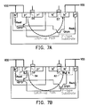
- FIG. 7A is a cross sectional view of a CMOS device without using the latch-up implantation
- FIG. 7B is a cross sectional view of a CMOS device using latch-up implantation
- FIG. 8 schematically illustrates the parasitic circuit of the CMOS device as shown in FIG. 7A;
- FIG. 9 schematically illustrates the parasitic circuit of the CMOS device as shown in FIG. 7B;
- FIG. 10A shows another embodiment of the parasitic circuit according to the invention.
- FIG. 10B shows also another embodiment of the parasitic circuit according to the invention.
- the bulk of the PMOS is coupled to the most positive voltage source, and the bulk of the NMOS is coupled to the most negative voltage source.
- a latch-up current path is easily induced. Under a normal operation condition, this latch-up current path is not conducted. However, if a noise is occurred to trigger the latch-up current path on, the parasitic SCR device is conducted to induce the latch-up effect, and thus, the IC is blown.
- a method to increase the impedance of the SCR conducting path is provided.
- the latch-up immunity for the CMOS is thus enhanced.
- an ion implantation which lightly doping is performed at a cathode or anode of the parasitic SCR device that the latch-up current is likely to occur.
- the impedance of the SCR conducting path is thus increased.
- This method is referred as latch-up implantation.
- the parasitic SCR device thus has a higher resistance against the noise and is not easily to be conducted thereby.
- latch-up implantation to increase the impedance of the SCR conducting path, so as to prevent latch-up effect does not require any additional silicon area, thus greatly increase the flexibility of circuit design.
- FIG. 5 shows a layout pattern of the invention. Different from the conventional CMOS device layout pattern, the mask patterns for latch-up implantation are used.
- the mask pattern 40 for latch-up implantation can be used for PMOS or NMOS.
- the reference numeral 42 indicates the latch-up implanting region for PMOS, while the reference numeral 44 indicates the latch-up implanting region for NMOS.
- FIG. 6A to FIG. 6E shows a brief flowchart of a conventional CMOS fabrication process with an additional step of the latch-up implantation.
- a substrate 50 for example, a P-type substrate, is provided.
- a photoresist layer 52 is formed to cover a portion of the substrate 50 .
- the substrate 50 exposed by the photoresist layer 52 is implanted with N type ions to form an N-well 56 .
- the photoresist layer 52 is removed.
- An oxide layer and a polysilicon layer are sequentially formed on the substrate 50 including the N-well 56 .
- the oxide layer and the polysilicon layer are then patterned to respectively form a gate oxide 57 and a gate 58 on the P-type substrate 50 , and a gate oxide 59 and a gate 60 on the N-well 56 .
- a photoresist layer 62 is formed on the substrate 50 including the N-well 56 .
- the photoresist layer 62 covers a portion of the N-well 56 , the gate 60 and a portion of the P-type substrate 50 , while exposing the second gate 58 and a region near the first gate 60 .
- An NMOS source/drain implantation 64 is performed. That is, using the photoresist layer 62 as a mask, a heavily doped source region 66 and a heavily doped drain region 68 are formed aside of the gate 58 , and a heavily doped N-type region 70 (N + -region) is formed in the N-well 56 . Thus far, an NMOS including the source region 66 , the drain region 68 and the gate 58 is formed. The photoresist layer 62 is then removed.
- another photoresist layer 72 is formed on the substrate 50 including the N-well 56 .
- the photoresist layer 72 covers the whole P-type substrate 50 including the NMOS, except a portion near and with a distance to the source region 66 .
- the photoresist layer 72 further covers a portion of the N-well 56 , and exposes the gate 60 and a region next to the gate 60 .
- a PMOS source/drain implantation is performed.
- p-type ions 74 are implanted into the P-type substrate 50 and the N-well 56 heavily to form a source region 78 and a drain region 76 around the gate 60 in the N-well 56 , and a heavily dope P-type region 80 (P + -region) in the P-type substrate 50 .
- the photoresist layer 72 is then removed.
- an NMOS is formed in the P-type substrate 50 , and a PMOS including the source region 78 , the drain region 76 and the gate 60 is formed in the N-well 56 .
- an N ⁇ -region 70 is formed near and with a distance to the source region 78 in the N-well 56
- a P + -region 80 is formed near and with a distance to the source region 66 in the P-type substrate 50 .
- lightly doped regions including P-region 84 and N-region 82 are formed in the N-well 56 and the substrate 50 , respectively.
- the lightly doped P-region 84 is located at the same place with the source region 78 and deeper than source region 78 but shallower than the N-well 56 .
- the lightly doped N-region 82 is located at the same place with the source region 66 and deeper than the source region 66 .
- the following two process sequences of forming the lightly doped P-region 84 and the lightly doped N-region 82 can be interchanged.
- a photoresist layer is formed on the P-type substrate and the N-well 56 and exposing a portion located at the same place with the source region 78 but larger than the source region 78 .
- the first type same with the p + region latch-up implantation is performed to form the lightly doped P-region and the photoresist layer is removed.
- another photoresist layer is formed on the P-type substrate 50 and the N-well 56 , and exposing a portion located at the same place with the source region 66 but larger than the source region 66 .
- the second type same with n + region latch-up implantation is performed to form the lightly doped N-region 82 , and the photoresist layer is then removed.
- a P-well can also be formed in an N-type substrate with a structure the same as shown in FIGS. 6A to 6 E, while the conductive types of N and P of the above structure are interchanged. Also, the process shown in FIG. 6E could be done before performing the process shown in FIGS. 6C and 6D.
- FIG. 7A shows a path that latch-up phenomenon may happen in CMOS circuits.
- the latch-up path is illustrated as a dash line in FIG. 7 A.
- the turning on the parasitic BJTs Q pnp and Q npn is the main cause of the latch-up phenomenon as mentioned.
- two lightly doped regions 84 and 82 are the only difference. These two lightly doped regions are latch-up implantation regions. Adding the latch-up implantation regions can increase the intrinsic resistance in the emitter of the parasitic Q pnp and Q npn and thus the bias of emitter-base junction can be reduced.
- the formation of the latch-up implanting regions 82 and 84 equivalently adds a resistor R P in the emitter of the Q pnp and a resistor R N in the emitter of the Q npn .
- the increased impedance thus raise the threshold for the occurrence of the latch-up.
- there is no alteration for the channels of the NMOS and the PMOS therefore, the original I-V characteristics thereof is not altered. That is, both the transistors PMOS and NMOS can work normally without being affected by the latch-up implantation.
- FIG. 8 and FIG. 9 show the equivalent parasitic circuit diagrams of the CMOS device as shown in FIGS. 7A and 7B, respectively.
- the additional latch-up implantation produces the additional resistors R P and R N .
- R N in the emitter of the BJT Q npn
- the noise level which can trigger on the BJT Q npn is arose.
- R P in the emitter of the BJT Q pnp
- the noise level which can trigger on the BJT Q pnp is arose.
- the noise level which can trigger on the whole SRC device is arose, and the immunity of latch-up effect of the CMOS circuit is improved.
- the structure may be formed to include either one of the resistors R P or R N (as shown in FIGS. 10A and 10B, respectively). That is, referring to the explanation of FIG. 6E, the two process steps of lightly doped regions 84 and 82 may be performed only one of them.
- the latch-up implanting of lightly doped regions 82 is the only one latch-up implantation process step performed.
- latch-up implanting of the lightly doped region 84 is the only one latch-up implantation process step performed. Whether one or two latch-up implanting regions are formed depends on specific requirements.
- the invention can be applied to digital CMOS circuit design, analog CMOS circuit design, and power device that have a high demand in latch-up prevention.
Abstract
Description
Claims (21)
Applications Claiming Priority (2)
| Application Number | Priority Date | Filing Date | Title |
|---|---|---|---|
| TW89101682A | 2000-02-01 | ||
| TW089101682A TW451423B (en) | 2000-02-01 | 2000-02-01 | Latch-up structure for improving CMOS processing using latch-up ion implantation and the manufacturing method thereof |
Publications (1)
| Publication Number | Publication Date |
|---|---|
| US6465283B1 true US6465283B1 (en) | 2002-10-15 |
Family
ID=21658671
Family Applications (1)
| Application Number | Title | Priority Date | Filing Date |
|---|---|---|---|
| US09/654,810 Expired - Lifetime US6465283B1 (en) | 2000-02-01 | 2000-09-05 | Structure and fabrication method using latch-up implantation for improving latch-up immunity in CMOS fabrication process |
Country Status (2)
| Country | Link |
|---|---|
| US (1) | US6465283B1 (en) |
| TW (1) | TW451423B (en) |
Cited By (19)
| Publication number | Priority date | Publication date | Assignee | Title |
|---|---|---|---|---|
| US6737682B1 (en) * | 2002-07-30 | 2004-05-18 | Taiwan Semiconductor Manufacturing Company | High voltage tolerant and low voltage triggering floating-well silicon controlled rectifier on silicon-on-insulator for input or output |
| US20040253776A1 (en) * | 2003-06-12 | 2004-12-16 | Thomas Hoffmann | Gate-induced strain for MOS performance improvement |
| WO2005031965A2 (en) | 2003-09-25 | 2005-04-07 | Silicon Laboratories, Inc. | Stacked rf power amplifier |
| US20050247980A1 (en) * | 2004-03-25 | 2005-11-10 | Microchip Technology Incorporated | High voltage ESD-protection structure |
| US20050270710A1 (en) * | 2004-06-02 | 2005-12-08 | National Chiao Tung University | Silicon controlled rectifier for the electrostatic discharge protection |
| US20050286295A1 (en) * | 2004-06-25 | 2005-12-29 | Kapre Ravindra M | Memory cell array latchup prevention |
| US20060289941A1 (en) * | 2005-06-22 | 2006-12-28 | Infineon Technologies Ag | Transistor component |
| US20070018193A1 (en) * | 2005-07-21 | 2007-01-25 | Industrial Technology Research Institute | Initial-on SCR device for on-chip ESD protection |
| US20080124884A1 (en) * | 2006-08-28 | 2008-05-29 | Pelella Mario M | Methods for fabricating a semiconductor device on an soi substrate |
| US7408228B2 (en) | 2003-03-27 | 2008-08-05 | Mitsubishi Denki Kabushiki Kaisha | Semiconductor device capable of avoiding latchup breakdown resulting from negative variation of floating offset voltage |
| EP2079111A1 (en) * | 2008-01-10 | 2009-07-15 | Khaje Nasir Toosi University of Technology Seyyed Khandan Brdg. | Nanoscale CMOS transister with an intrinsic bulk |
| US20090261378A1 (en) * | 2005-07-07 | 2009-10-22 | Intersil Americas Inc. | Devices with adjustable dual-polarity trigger - and holding-voltage/current for high level of electrostatic discharge protection in sub-micron mixed signal cmos/bicmos integrated |
| US20100034000A1 (en) * | 2008-07-04 | 2010-02-11 | Stmicroelectronics (Rousset) Sas | Electronic circuit having a diode-connected mos transistor with an improved efficiency |
| EP2293338A2 (en) | 2003-06-16 | 2011-03-09 | Intel Corporation | Double-gate transistor with enhanced carrier mobility field |
| USRE42232E1 (en) | 2001-09-21 | 2011-03-22 | Intellectual Ventures I Llc | RF chipset architecture |
| US20140035039A1 (en) * | 2012-04-23 | 2014-02-06 | Taiwan Semiconductor Manufacturing Co., Ltd. | Electrostatic discharge (esd) guard ring protective structure |
| US8686532B2 (en) * | 2004-11-16 | 2014-04-01 | Renesas Electronics Corporation | Semiconductor device having an annular guard ring |
| US8987067B2 (en) | 2013-03-01 | 2015-03-24 | International Business Machines Corporation | Segmented guard ring structures with electrically insulated gap structures and design structures thereof |
| US9842629B2 (en) | 2004-06-25 | 2017-12-12 | Cypress Semiconductor Corporation | Memory cell array latchup prevention |
Citations (10)
| Publication number | Priority date | Publication date | Assignee | Title |
|---|---|---|---|---|
| US4380021A (en) * | 1979-03-22 | 1983-04-12 | Hitachi, Ltd. | Semiconductor integrated circuit |
| US4603471A (en) * | 1984-09-06 | 1986-08-05 | Fairchild Semiconductor Corporation | Method for making a CMOS circuit having a reduced tendency to latch by controlling the band-gap of source and drain regions |
| US5293051A (en) * | 1992-02-14 | 1994-03-08 | Sharp Kabushiki Kaisha | Photoswitching device including a MOSFET for detecting zero voltage crossing |
| US5523246A (en) * | 1995-06-14 | 1996-06-04 | United Microelectronics Corporation | Method of fabricating a high-voltage metal-gate CMOS device |
| US5637900A (en) * | 1995-04-06 | 1997-06-10 | Industrial Technology Research Institute | Latchup-free fully-protected CMOS on-chip ESD protection circuit |
| US5770504A (en) * | 1997-03-17 | 1998-06-23 | International Business Machines Corporation | Method for increasing latch-up immunity in CMOS devices |
| US5821589A (en) * | 1997-03-19 | 1998-10-13 | Genus, Inc. | Method for cmos latch-up improvement by mev billi (buried implanted layer for laternal isolation) plus buried layer implantation |
| US5831313A (en) * | 1996-08-15 | 1998-11-03 | Integrated Device Technology, Inc. | Structure for improving latch-up immunity and interwell isolation in a semiconductor device |
| US5861330A (en) * | 1997-05-07 | 1999-01-19 | International Business Machines Corporation | Method and structure to reduce latch-up using edge implants |
| US5879967A (en) * | 1996-01-26 | 1999-03-09 | Samsung Electronics Co., Ltd. | Methods forming power semiconductor devices having latch-up inhibiting regions |
-
2000
- 2000-02-01 TW TW089101682A patent/TW451423B/en not_active IP Right Cessation
- 2000-09-05 US US09/654,810 patent/US6465283B1/en not_active Expired - Lifetime
Patent Citations (10)
| Publication number | Priority date | Publication date | Assignee | Title |
|---|---|---|---|---|
| US4380021A (en) * | 1979-03-22 | 1983-04-12 | Hitachi, Ltd. | Semiconductor integrated circuit |
| US4603471A (en) * | 1984-09-06 | 1986-08-05 | Fairchild Semiconductor Corporation | Method for making a CMOS circuit having a reduced tendency to latch by controlling the band-gap of source and drain regions |
| US5293051A (en) * | 1992-02-14 | 1994-03-08 | Sharp Kabushiki Kaisha | Photoswitching device including a MOSFET for detecting zero voltage crossing |
| US5637900A (en) * | 1995-04-06 | 1997-06-10 | Industrial Technology Research Institute | Latchup-free fully-protected CMOS on-chip ESD protection circuit |
| US5523246A (en) * | 1995-06-14 | 1996-06-04 | United Microelectronics Corporation | Method of fabricating a high-voltage metal-gate CMOS device |
| US5879967A (en) * | 1996-01-26 | 1999-03-09 | Samsung Electronics Co., Ltd. | Methods forming power semiconductor devices having latch-up inhibiting regions |
| US5831313A (en) * | 1996-08-15 | 1998-11-03 | Integrated Device Technology, Inc. | Structure for improving latch-up immunity and interwell isolation in a semiconductor device |
| US5770504A (en) * | 1997-03-17 | 1998-06-23 | International Business Machines Corporation | Method for increasing latch-up immunity in CMOS devices |
| US5821589A (en) * | 1997-03-19 | 1998-10-13 | Genus, Inc. | Method for cmos latch-up improvement by mev billi (buried implanted layer for laternal isolation) plus buried layer implantation |
| US5861330A (en) * | 1997-05-07 | 1999-01-19 | International Business Machines Corporation | Method and structure to reduce latch-up using edge implants |
Non-Patent Citations (1)
| Title |
|---|
| Borland et al., "Epi Avoidance for CMOS Logic Devices Using MeV Implantation", Proceedings of the 11th International Conference on Ion Implantation Technology, Jun. 16-21, 1996, pp. 21-24. * |
Cited By (45)
| Publication number | Priority date | Publication date | Assignee | Title |
|---|---|---|---|---|
| USRE42232E1 (en) | 2001-09-21 | 2011-03-22 | Intellectual Ventures I Llc | RF chipset architecture |
| US6737682B1 (en) * | 2002-07-30 | 2004-05-18 | Taiwan Semiconductor Manufacturing Company | High voltage tolerant and low voltage triggering floating-well silicon controlled rectifier on silicon-on-insulator for input or output |
| DE102004064209B3 (en) | 2003-03-27 | 2018-03-15 | Mitsubishi Denki K.K. | Semiconductor module for driving a switching element |
| DE102004014744B4 (en) * | 2003-03-27 | 2013-02-07 | Mitsubishi Denki K.K. | A semiconductor device with a trench for driving a switching element and avoiding a latch-up breakthrough |
| US7777279B2 (en) | 2003-03-27 | 2010-08-17 | Mitsubishi Denki Kabushiki Kaisha | Semiconductor device capable of avoiding latchup breakdown resulting from negative variation of floating offset voltage |
| US7545005B2 (en) | 2003-03-27 | 2009-06-09 | Mitsubishi Denki Kabushiki Kaisha | Semiconductor device capable of avoiding latchup breakdown resulting from negative variation of floating offset voltage |
| US20080272440A1 (en) * | 2003-03-27 | 2008-11-06 | Mitsubishi Denki Kabushiki Kaisha | Semiconductor device capable of avoiding latchup breakdown resulting from negative variation of floating offset voltage |
| US20080265334A1 (en) * | 2003-03-27 | 2008-10-30 | Mitsubishi Denki Kabushiki Kaisha | Semiconductor device capable of avoiding latchup breakdown resulting from negative variation of floating offset voltage |
| US7408228B2 (en) | 2003-03-27 | 2008-08-05 | Mitsubishi Denki Kabushiki Kaisha | Semiconductor device capable of avoiding latchup breakdown resulting from negative variation of floating offset voltage |
| US6982433B2 (en) | 2003-06-12 | 2006-01-03 | Intel Corporation | Gate-induced strain for MOS performance improvement |
| US20040253776A1 (en) * | 2003-06-12 | 2004-12-16 | Thomas Hoffmann | Gate-induced strain for MOS performance improvement |
| US7452764B2 (en) | 2003-06-12 | 2008-11-18 | Intel Corporation | Gate-induced strain for MOS performance improvement |
| US20050167652A1 (en) * | 2003-06-12 | 2005-08-04 | Thomas Hoffmann | Gate-induced strain for MOS performance improvement |
| EP2293338A2 (en) | 2003-06-16 | 2011-03-09 | Intel Corporation | Double-gate transistor with enhanced carrier mobility field |
| WO2005031965A2 (en) | 2003-09-25 | 2005-04-07 | Silicon Laboratories, Inc. | Stacked rf power amplifier |
| EP1673858B1 (en) * | 2003-09-25 | 2018-10-24 | QUALCOMM Incorporated | Stacked rf power amplifier |
| US20050247980A1 (en) * | 2004-03-25 | 2005-11-10 | Microchip Technology Incorporated | High voltage ESD-protection structure |
| US7186594B2 (en) * | 2004-03-25 | 2007-03-06 | Microchip Technology Inc. | High voltage ESD-protection structure |
| US7542253B2 (en) * | 2004-06-02 | 2009-06-02 | National Chiao Tung University | Silicon controlled rectifier for the electrostatic discharge protection |
| US20050270710A1 (en) * | 2004-06-02 | 2005-12-08 | National Chiao Tung University | Silicon controlled rectifier for the electrostatic discharge protection |
| US20050286295A1 (en) * | 2004-06-25 | 2005-12-29 | Kapre Ravindra M | Memory cell array latchup prevention |
| US20090213677A1 (en) * | 2004-06-25 | 2009-08-27 | Kapre Ravindra M | Memory Cell Array |
| US8837245B2 (en) | 2004-06-25 | 2014-09-16 | Cypress Semiconductor Corporation | Memory cell array latchup prevention |
| US7773442B2 (en) * | 2004-06-25 | 2010-08-10 | Cypress Semiconductor Corporation | Memory cell array latchup prevention |
| US9842629B2 (en) | 2004-06-25 | 2017-12-12 | Cypress Semiconductor Corporation | Memory cell array latchup prevention |
| US8493804B2 (en) | 2004-06-25 | 2013-07-23 | Cypress Semiconductor Corporation | Memory cell array latchup prevention |
| US8045410B2 (en) | 2004-06-25 | 2011-10-25 | Cypress Semiconductor Corporation | Memory cell array |
| US8686532B2 (en) * | 2004-11-16 | 2014-04-01 | Renesas Electronics Corporation | Semiconductor device having an annular guard ring |
| US20060289941A1 (en) * | 2005-06-22 | 2006-12-28 | Infineon Technologies Ag | Transistor component |
| DE102005028905A1 (en) * | 2005-06-22 | 2006-12-28 | Infineon Technologies Ag | Transistor component for complementary MOS logic circuit, has substrate connecting contact arranged in substrate connecting region for conductively connecting substrate connecting region to supply voltage lead |
| US20090261378A1 (en) * | 2005-07-07 | 2009-10-22 | Intersil Americas Inc. | Devices with adjustable dual-polarity trigger - and holding-voltage/current for high level of electrostatic discharge protection in sub-micron mixed signal cmos/bicmos integrated |
| US7985640B2 (en) * | 2005-07-07 | 2011-07-26 | Intersil Americas, Inc. | Devices with adjustable dual-polarity trigger-and holding-voltage/current for high level of electrostatic discharge protection in sub-micron mixed signal CMOS/BiCMOS integrated |
| US8283695B2 (en) | 2005-07-07 | 2012-10-09 | Intersil Americas Inc. | Devices with adjustable dual-polarity trigger- and holding-votage/current for high level of electrostatic discharge protection in sub-micron mixed signal CMOS/BiCMOS integrated |
| US8102001B2 (en) | 2005-07-21 | 2012-01-24 | Industrial Technology Research Institute | Initial-on SCR device for on-chip ESD protection |
| US20110013326A1 (en) * | 2005-07-21 | 2011-01-20 | Industrial Technology Research Institute | Initial-on scr device for on-chip esd protection |
| US20070018193A1 (en) * | 2005-07-21 | 2007-01-25 | Industrial Technology Research Institute | Initial-on SCR device for on-chip ESD protection |
| US7825473B2 (en) * | 2005-07-21 | 2010-11-02 | Industrial Technology Research Institute | Initial-on SCR device for on-chip ESD protection |
| US20080124884A1 (en) * | 2006-08-28 | 2008-05-29 | Pelella Mario M | Methods for fabricating a semiconductor device on an soi substrate |
| US7465623B2 (en) * | 2006-08-28 | 2008-12-16 | Advanced Micro Devices, Inc. | Methods for fabricating a semiconductor device on an SOI substrate |
| EP2079111A1 (en) * | 2008-01-10 | 2009-07-15 | Khaje Nasir Toosi University of Technology Seyyed Khandan Brdg. | Nanoscale CMOS transister with an intrinsic bulk |
| US20100034000A1 (en) * | 2008-07-04 | 2010-02-11 | Stmicroelectronics (Rousset) Sas | Electronic circuit having a diode-connected mos transistor with an improved efficiency |
| US8445947B2 (en) * | 2008-07-04 | 2013-05-21 | Stmicroelectronics (Rousset) Sas | Electronic circuit having a diode-connected MOS transistor with an improved efficiency |
| US8809961B2 (en) * | 2012-04-23 | 2014-08-19 | Taiwan Semiconductor Manufacturing Co., Ltd. | Electrostatic discharge (ESD) guard ring protective structure |
| US20140035039A1 (en) * | 2012-04-23 | 2014-02-06 | Taiwan Semiconductor Manufacturing Co., Ltd. | Electrostatic discharge (esd) guard ring protective structure |
| US8987067B2 (en) | 2013-03-01 | 2015-03-24 | International Business Machines Corporation | Segmented guard ring structures with electrically insulated gap structures and design structures thereof |
Also Published As
| Publication number | Publication date |
|---|---|
| TW451423B (en) | 2001-08-21 |
Similar Documents
| Publication | Publication Date | Title |
|---|---|---|
| US6465283B1 (en) | Structure and fabrication method using latch-up implantation for improving latch-up immunity in CMOS fabrication process | |
| US7494854B2 (en) | Turn-on-efficient bipolar structures for on-chip ESD protection | |
| US7274047B2 (en) | Silicon controlled rectifier electrostatic discharge protection device for power supply lines with powerdown mode of operation | |
| US6909149B2 (en) | Low voltage silicon controlled rectifier (SCR) for electrostatic discharge (ESD) protection of silicon-on-insulator technologies | |
| US6791122B2 (en) | Silicon controlled rectifier electrostatic discharge protection device with external on-chip triggering and compact internal dimensions for fast triggering | |
| JP3058203U (en) | Fully protected CMOS on-chip ESD protection circuit without latch-up | |
| US7875933B2 (en) | Lateral bipolar transistor with additional ESD implant | |
| KR100275962B1 (en) | Semiconductor device and manufacturing method thereof | |
| US20050212051A1 (en) | Low voltage silicon controlled rectifier (SCR) for electrostatic discharge (ESD) protection of silicon-on-insulator technologies | |
| US20020109190A1 (en) | Method for forming a lateral SCR device for on-chip ESD protection in shallow-trench-isolation CMOS process | |
| US20020003266A1 (en) | Apparatus improving latchup immunity in a dual-polysilicon gate | |
| US7718481B2 (en) | Semiconductor structure and method of manufacture | |
| US6614078B2 (en) | Highly latchup-immune CMOS I/O structures | |
| US9685443B2 (en) | Compact guard ring structure for CMOS integrated circuits | |
| US6777721B1 (en) | SCR device for ESD protection | |
| US5883414A (en) | Electrostatic discharge protection device | |
| US8107203B2 (en) | Electrostatic discharge protection device | |
| US5990520A (en) | Method for fabricating a high performance vertical bipolar NPN or PNP transistor having low base resistance in a standard CMOS process | |
| US6670678B2 (en) | Semiconductor device having ESD protective transistor | |
| US7326998B1 (en) | Effective I/O ESD protection device for high performance circuits | |
| US6476451B2 (en) | Buried guard rings for CMOS device | |
| US6831346B1 (en) | Buried layer substrate isolation in integrated circuits | |
| US7955923B1 (en) | I/O ESD protection device for high performance circuits | |
| EP0772237B1 (en) | Semiconductor device including protection means | |
| US6894320B2 (en) | Input protection circuit |
Legal Events
| Date | Code | Title | Description |
|---|---|---|---|
| AS | Assignment |
Owner name: INDUSTRIAL TECHNOLOGY RESEARCH INSTITUTE, TAIWAN Free format text: ASSIGNMENT OF ASSIGNORS INTEREST;ASSIGNORS:CHANG, CHYH-YIH;KER, MING-DOU;JIANG, HSIN-CHIN;AND OTHERS;REEL/FRAME:011090/0169 Effective date: 20000717 |
|
| STCF | Information on status: patent grant |
Free format text: PATENTED CASE |
|
| FPAY | Fee payment |
Year of fee payment: 4 |
|
| AS | Assignment |
Owner name: TRANSPACIFIC IP LTD., TAIWAN Free format text: ASSIGNMENT OF ASSIGNORS INTEREST;ASSIGNOR:INDUSTRIAL TECHNOLOGY RESERACH INSTITUTE;REEL/FRAME:018498/0272 Effective date: 20060610 |
|
| FPAY | Fee payment |
Year of fee payment: 8 |
|
| FPAY | Fee payment |
Year of fee payment: 12 |