US6437381B1 - Semiconductor memory device with reduced orientation-dependent oxidation in trench structures - Google Patents
Semiconductor memory device with reduced orientation-dependent oxidation in trench structures Download PDFInfo
- Publication number
- US6437381B1 US6437381B1 US09/560,081 US56008100A US6437381B1 US 6437381 B1 US6437381 B1 US 6437381B1 US 56008100 A US56008100 A US 56008100A US 6437381 B1 US6437381 B1 US 6437381B1
- Authority
- US
- United States
- Prior art keywords
- layer
- trench
- isolation collar
- oxide layer
- gate
- Prior art date
- Legal status (The legal status is an assumption and is not a legal conclusion. Google has not performed a legal analysis and makes no representation as to the accuracy of the status listed.)
- Expired - Fee Related
Links
Images


Classifications
-
- H—ELECTRICITY
- H10—SEMICONDUCTOR DEVICES; ELECTRIC SOLID-STATE DEVICES NOT OTHERWISE PROVIDED FOR
- H10B—ELECTRONIC MEMORY DEVICES
- H10B12/00—Dynamic random access memory [DRAM] devices
- H10B12/01—Manufacture or treatment
- H10B12/02—Manufacture or treatment for one transistor one-capacitor [1T-1C] memory cells
- H10B12/05—Making the transistor
- H10B12/053—Making the transistor the transistor being at least partially in a trench in the substrate
-
- H—ELECTRICITY
- H10—SEMICONDUCTOR DEVICES; ELECTRIC SOLID-STATE DEVICES NOT OTHERWISE PROVIDED FOR
- H10B—ELECTRONIC MEMORY DEVICES
- H10B12/00—Dynamic random access memory [DRAM] devices
- H10B12/01—Manufacture or treatment
- H10B12/02—Manufacture or treatment for one transistor one-capacitor [1T-1C] memory cells
- H10B12/03—Making the capacitor or connections thereto
- H10B12/038—Making the capacitor or connections thereto the capacitor being in a trench in the substrate
- H10B12/0383—Making the capacitor or connections thereto the capacitor being in a trench in the substrate wherein the transistor is vertical
Definitions
- the present invention relates generally to vertical transistor structures in the trench capacitors of Dynamic Random Access Memory (DRAM) cells and, more specifically, to a process for manufacture of such structures.
- DRAM Dynamic Random Access Memory
- FIG. 1 schematically illustrates a typical semiconductor memory device.
- FIG. 12 A more detailed depiction of such a semiconductor memory device is provided in FIG. 12 .
- Semiconductor memory device 10 comprises a capacitor trench 12 , an isolation or “trench top” oxide (TTO) 14 , a gate oxide 16 , diffusion regions (contact implants) 18 , a gate contact 220 , a source contact 222 , and gate sidewall isolation spacers 240 .
- TTO isolation or “trench top” oxide
- FIG. 2 is a cross section taken along line 2 — 2 in FIG. 1 .
- gate oxide 16 forms a continuous faceted wall formed of planes aligned with the ( 100 ) and ( 110 ) crystal planes for a silicon wafer with a ( 100 ) surface orientation.
- the silicon wafer may have any surface orientation, however, as is known in the art.
- a crystal contains planes of atoms which influence the properties and behavior of a material.
- such identification is done using Miller indices: three numbers within parentheses, namely (hkl).
- the Miller indices are the reciprocals of the three axial intercepts for a plane, cleared of fractions and common multipliers.
- brackets which refer to families of equivalent crystallographic planes (e.g., the ⁇ 001 ⁇ family of planes); parentheses, ( ), which refer to specific crystallographic planes (e.g., the (100) plane); horizontal triangles, ⁇ , which refer to families of equivalent crystallographic axes (e.g., the ⁇ 011> family of axes); and square brackets, [ ], which refer to a specific crystal axis (e.g., the [110] axis).
- the (100) plane and the (001) plane are equivalent to one another and, thus, are both in the same ⁇ 001 ⁇ family of planes.
- the oxidation step used to form gate oxide 16 is strongly crystal orientation dependent. That is, the thickness of the oxide formed after a given time at a given temperature is dependent on the crystal orientation of the underlying silicon. Thus, the gate oxidation step tends to form gate oxide 16 with a thickness d 1 in the (110) planes that is greater than thickness d 2 in the (100) planes.
- the non-homogenous gate oxide thickness leads to weak points at the thinner sections where the time to breakdown is reduced relative to the rest of the gate oxide.
- FIGS. 3-12 in which like reference numbers refer to like elements throughout, there is shown various aspects of an exemplary DRAM cell and intermediate steps in an exemplary process for making the cell. These process steps are disclosed by U.S. patent application Ser. No. 09/359,292 filed on behalf of Gary Bronner et al., assigned to the common assignee of this invention, and incorporated herein by reference.
- a typical deep trench storage capacitor of semiconductor memory device 10 is formed into a pad 22 and a substrate 24 by conventional processing techniques well known in the art. For example, an optical lithography step may be used to form a pattern on pad 22 . Then a dry etching step, such reactive-ion etching (RIE), may be used to create a trench 20 to a desired depth through pad 22 and into substrate 24 .
- RIE reactive-ion etching
- Deep trench 20 generally has a depth of about 3 ⁇ m to about 10 ⁇ m and a diameter or maximum width that is a function of the lithographic ground rule, typically about 0.5 ⁇ m to less than 0.1 ⁇ m.
- Trench 20 has sidewalls 32 and a bottom 33 .
- an isolation collar 26 is formed in an upper region 28 of trench 20 .
- Upper region 28 typically comprises 10-20% of the total depth of trench 20 .
- Collar 26 may be formed using a local thermal oxidation (LOCOS) process, such as by the exemplary process explained below, or by other physical and chemical mechanisms, as also indicated below. Because of the traditional use of the LOCOS process, isolation collar 26 is sometimes referred to as a LOCOS collar.
- LOCOS local thermal oxidation
- a barrier film (not shown) may be formed along the exposed surfaces of trench 20 and pad 22 such as by a low-pressure chemical vapor deposition (LPCVD) of a SiN film having a thickness of about 2 nm to about 10 nm.
- LPCVD low-pressure chemical vapor deposition
- the barrier film is then removed from upper region 28 , for example by filling trench 20 with photoresist (not shown) and partially etching the photoresist down into trench 20 to a depth controlled by the amount of overetch time.
- This step exposes the barrier film in upper region 28 while leaving the lower region 30 covered.
- the exposed barrier film may then be removed in upper region 28 of trench 20 and from pad layer 22 , for example, by chemical or dry etching, and then the photoresist stripped away.
- Other processes for isolating sidewall 32 in upper region 28 while protecting sidewall 32 in lower region 30 may also be used.
- the local oxidation step is then performed.
- the oxidation step may be conducted, for example, at oxidation conditions that promote the oxidation rate along one family of crystal axes over another. Such oxidation conditions induce faceting of the underlying silicon substrate 24 during growth of collar 26 .
- Such a faceted collar may have a cross section similar to that shown for gate oxide 16 as illustrated in FIG. 2, where thickness di of the oxide aligned with one plane is greater than thickness d 2 of the oxide aligned with another crystal plane. Because of the different oxidation rates of the different crystal orientations, in order to achieve a minimum collar thickness on all of the sidewalls, regardless of crystal orientation, an unnecessary, increased thickness may be required on the sidewall having the faster-growing orientation.
- the thermal oxide collar 26 and associated faceting are formed only on sidewalls 32 in upper region 28 of trench 20 ; the barrier film protects sidewalls 32 in lower region 30 of trench 20 .
- Buried plate 34 may be created by doping lower region 30 of trench 20 to form an out-diffusion in substrate 24 using collar 26 as a mask for upper region 28 .
- the out-diffusion may be formed using arsenosilicate glass (ASG) drive-in, plasma doping (PLAD), plasma ion implantation (PIII), gas-phase diffusion of arsenic (As) or phosphorus (P), or other techniques known in the art.
- a thin node dielectric 35 is created, such as by thermal nitridation, for example with ammonia (NH 3 ), followed by LPCVD of SiN.
- trench 20 is filled, such as with an n+ doped LPCVD polysilicon 36 , and recessed to a desired depth D 1 .
- Depth D 1 is typically about 300 nm to about 700 nm, preferably between 300 to 450 nm.
- Isolation collar 26 is then etched away, such as with a wet etch using a solution containing hydrogen fluoride (HF), to expose sidewalls 32 in the area where the collar 26 is not covered by polysilicon 36 and below the polysilicon level to a depth D 2 , as shown in FIG. 6.
- D 2 is typically about 10 nm to about 50 nm.
- a buried strap 40 is formed.
- buried strap 40 is formed in a layer having a thickness of about 10 nm to about 50 nm.
- buried strap 40 is then removed from sidewalls 32 of trench 20 above polysilicon 36 and above pad 22 , such as by an isotropic wet chemical or dry etching step.
- trench-top dielectric 14 or trench-top oxide (TTO) is formed, such as by an anisotropic high-density plasma (HDP) or other bias-assisted oxide deposition step.
- HDP high-density plasma
- the creation of trench-top dielectric 14 typically forms a corresponding layer (not shown) atop pad 22 , which is removed by a chemical mechanical polishing (CMP) step as is known in the art.
- CMP chemical mechanical polishing
- pad 22 is then stripped, typically by a wet chemical etch step selective to trench-top dielectric 14 , and a sacrificial oxide 44 is grown on the exposed surface of substrate 24 and exposed sidewall 32 of trench 20 , as shown in FIG. 9 .
- Ion implantation may then be used to create a p-well 50 and an n-band 52 below p-well 50 in substrate 24 .
- ion implantation of As or P may be used to create diffusion region 18 .
- Another diffusion region 62 is created by out-diffusion from n+ doped polysilicon region 36 through buried strap 40 . Such process steps yield the structure shown in FIG. 9 .
- Other device-threshold-tailoring implants may also be created at this time.
- sacrificial oxide 44 is removed, such as by a chemical wet etch process with an HF-containing solution.
- gate oxide 16 is grown and a conductive gate layer 48 , such as polysilicon having a thickness approximately equal to the diameter of trench 20 , is formed.
- a nitride pad (not shown) is formed having a thickness of approximately half to approximately equal to the thickness of gate layer 48 .
- An active area 54 is patterned (see FIG. 11 ), typically by photolithography, and an etching step, such as RIE, is performed to etch shallow trench isolation (STI) regions 46 everywhere except in active area 54 .
- STI regions 46 are filled, typically with an oxide, and planarized by a CMP step down to the pad nitride. The pad nitride is then stripped away, leaving the structure shown in FIG. 10 .
- a thin seed layer of polysilicon is typically deposited, extending polysilicon gate layer 48 over the edge of trench 20 and over top diffusion region 62 in p-well 50 of substrate 24 .
- a middle layer 56 which typically comprises a higher conductivity material than polysilicon gate layer 48 , such as tungsten (W) or tungsten silicide (WS), is then formed.
- a gate cap layer 58 comprising SiN or silicon oxide, is formed.
- the gate conductor layers are then patterned by lithography and dry etched, leaving the gate contact 220 (comprising gate layer 48 , middle layer 56 , and gate cap 58 ) shown in FIG. 12 .
- sidewall isolation spacers 240 typically comprising silicon nitride, silicon oxide, or a combination of those materials, are created by processes well-known in the art to electrically isolate the wordline (gate contact 220 ) from the bitline (the source or diffusion contact 222 ).
- Spacers 240 are typically created by depositing a conformal coating of SiN of about 10 nm to about 100 nm, and performing an anisotropic dry spacer etch process to leave the spacers 240 only on the sidewalls of gate contact 220 .
- optional added implants may be performed to tailor source and drain regions (diffusion regions 18 and 62 ) of the transistor.
- Source contact 222 typically comprises doped polysilicon or a tungsten stud.
- the overlapping region 72 of source contact 222 and of gate cap layer 58 of gate contact 220 is typical of diffusion contacts known as borderless contacts.
- an exemplary trench-sidewall array device 60 results from the exemplary process described above.
- n+ diffusion regions 18 , 62 under diffusion contact 64 adjacent to trench 20 serve as the source and drain of device 60 .
- a channel 66 results in substrate 24 (p-well 50 ) adjacent faceted sidewalls 32 of trench 20 .
- device 60 as shown in FIG. 11 has been fabricated across the (011) plane, device 60 may also be fabricated across the (001) plane.
- the surface of substrate 24 is typically along the (100) plane.
- device 60 may be along a crystallographic plane in the same family as the substrate surface ⁇ 001 ⁇ , or may be on a different crystallographic plane (011) in a different family, as shown in FIG. 11 .
- the differential oxide wall thickness causes undesired effects. Among those effects are potential dislocations.
- the present invention provides a process, and a semiconductor memory device manufactured by that process, for reducing the undesired effects of orientation-dependent oxidation and avoiding such potential dislocations.
- the conventional process described above resulting in the above structure is merely one exemplary process for creating a DRAM cell having a vertical transistor.
- Other processes known in the art can similarly benefit from the improvements of the present invention.
- the present invention provides a process for forming an oxide layer on a sidewall of a trench in a substrate.
- the process comprises the steps of forming the trench in the substrate; forming a nitride interface layer over a portion of the trench sidewall; forming an amorphous layer over the nitride interface layer; and oxidizing the amorphous layer to form the oxide layer.
- the oxidation step is preferably of sufficient duration to completely consume the amorphous layer over the nitride interface layer.
- the oxidation step may further be of sufficient duration, however, to oxidize a portion of the trench sidewall under the nitride interface layer.
- the amorphous layer is formed having a thickness that is approximately half of a desired oxide layer thickness.
- the amorphous layer may have a thickness of about 25 to about 50 Angstroms when the oxide layer grows to a thickness of about 50 to about 100 Angstroms.
- the process may be used, for example, to form a gate oxide for a vertical transistor, or an isolation collar. Where the process is used to form an isolation collar, the process further comprises forming a nitride-oxynitride barrier layer over the amorphous silicon layer, and then etching away a portion of the nitride-oxynitride barrier layer to define the portion of the amorphous silicon to be oxidized.
- the invention also comprises a semiconductor memory device having a substrate and a trench in the substrate with a sidewall.
- An isolation collar comprising an isolation collar oxide layer is located on the trench sidewall in an upper portion of the trench.
- a vertical gate oxide comprising a gate oxide layer is located on the trench sidewall in the upper portion of the trench above the isolation collar.
- the isolation collar oxide layer may be disposed over an isolation collar nitride interface layer between the isolation collar oxide layer and the trench sidewall, the gate oxide layer may be disposed over a gate nitride interface layer between the gate oxide layer and the trench sidewall, or both.
- FIG. 1 is a longitudinal section of a schematic illustration of a typical DRAM device having a vertical transistor structure of the prior art
- FIG. 2 is a cross section of a portion of the gate oxide of the structure of FIG. 1 taken along line 2 — 2 ;
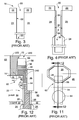
- FIGS. 3 through 10 are in-process longitudinal section illustrations depicting an exemplary process for manufacturing an exemplary DRAM as is known in the art and, more specifically, FIG. 3 shows a typical trench and pad layer;
- FIG. 4 shows an isolation collar formed in the upper region of the trench and a buried plate in the lower region of the trench
- FIG. 5 shows the trench of FIG. 4 after a dielectric is applied and the trench is partly filled with polysilicon
- FIG. 6 shows the trench of FIG. 5 after the collar is etched
- FIG. 7 shows the trench of FIG. 6 after a buried strap is formed
- FIG. 8 shows the trench of FIG. 7 after the buried strap is removed from the sidewalls of the trench above the polysilicon and above the pad;
- FIG. 9 shows the trench of FIG. 8 after a trench-top dielectric is formed, the pad is stripped, a sacrificial oxide is grown on the exposed surface of the substrate and on the exposed sidewall of the trench, a p-well and an n-band are created in the substrate, and diffusion regions are formed in the substrate;
- FIG. 10 shows the trench of FIG. 9 after the sacrificial oxide is removed, a gate oxide is grown, a conductive gate layer is formed, an active area is patterned, an etching step is performed to etch shallow trench isolation (STI) regions everywhere except in the active area, the STI regions are filled and planarized to the pad nitride, and the pad nitride is stripped away;
- STI shallow trench isolation
- FIG. 11 is a plan view illustration of an exemplary DRAM cell as is known in the art.
- FIG. 12 is a longitudinal section illustration of the DRAM cell of FIG. 11 taken along the line 12 — 12 ;
- FIG. 13 is an in-process longitudinal section illustration of a trench having an isolation collar manufactured by an exemplary process of the present invention, showing the amorphous silicon layer before oxidation;
- FIG. 14 is an in-process longitudinal section illustration of the trench of FIG. 13 just before an oxidation step to form a gate oxide layer by an exemplary process of the present invention
- FIG. 15 is an in-process longitudinal section illustration of the trench of FIG. 14 after formation of the gate oxide layer.
- FIG. 16 is a cross section of a portion of the gate oxide of the structure of FIG. 15 taken along the line 16 — 16 .
- FIG. 13 shows trench 200 on which isolation collar 130 is formed.
- the LOCOS process described in the background section of this application may be performed to carry out the oxidation, or other oxidation steps known in the art may be used.
- a nitride interface barrier film 125 is formed along the exposed surfaces of trench 200 and pad 22 , such as by a low-pressure chemical vapor deposition (LPCVD) step comprising exposing the surfaces to an atmosphere of NH 3 at 400-900° C., more preferably 500-700° C.
- Barrier film 125 is typically in a range of about 0.5 to 2 nm, and preferably about 1 nm thick.
- a-Si layer 127 Overtop of barrier film 125 is formed amorphous silicon (a-Si) layer 127 .
- the a-Si layer 127 may have a thickness in a range of about 5 nm to about 20 nm, with a preferred thickness of about 10 nm.
- a barrier film 129 such as a nitride-oxynitride film, is formed over a-Si layer 127 , such as by LPCVD of a SiN film having a thickness of about 2 nm to about 10 nm, preferably about 5.5 nm.
- nitride-oxynitride means that the film may be formed of silicon nitride, silicon oxynitride, or a combination of those materials.
- Barrier film 129 may then be removed from upper region 28 , for example by filling trench 200 with photoresist (not shown) and partially etching the photoresist down into trench 200 to a depth controlled by the amount of overetch time. This step exposes a portion of barrier film 129 in upper region 28 while leaving the portion in lower region 30 covered. The portion of barrier film 129 in upper region 28 of trench 20 and on pad layer 22 is then removed, for example, by a chemical or dry etching (CDE) recess step, and then the photoresist stripped away.
- CDE chemical or dry etching
- the local oxidation step is then performed, during which amorphous silicon layer 127 oxidizes into a silicon oxide layer to form oxide isolation collar 130 as is shown in FIG. 14 .
- Typical oxidation conditions are 800-900° C. in an oxygen atmosphere.
- the barrier film 129 , and optionally a-Si layer 127 and nitride interface layer 125 , in lower region 30 is typically stripped via a process that selectively leaves oxide isolation collar 130 in upper region 28 of trench 20 .
- a-Si layer 127 and interface film 125 in lower region 30 may remain temporarily if not removed in this step, both must be removed eventually.
- gate oxide 160 is then grown in accordance with the present invention.
- a nitride interface layer 1250 is formed as described above for the formation of interface layer 125 under the isolation collar 130 .
- amorphous layer 1270 is formed having a thickness of between about 1 to about 10 nm, preferably about 2.5 to about 5 nm, and more preferably about 3 nm.
- the gate oxide is grown from amorphous layer 1270 to form gate oxide layer 160 as is shown in FIG. 15 .
- Processing in accordance with the present invention leaves a nitride layer and an oxide layer over TTO 14 and over the top surface 21 of substrate 24 .
- the extra nitride and oxide layers over TTO 14 are beneficial as additional insulation, but can be removed if desired.
- the nitride and oxide layers over surface 21 can remain or be removed, depending upon the additional processing desired.
- both the isolation collar growth process and the vertical gate oxide growth process, described above, offer advantages over the prior art in that the oxide layer is formed from the amorphous layer that is deposited over the nitride interface layer. As a result, the oxide growth is independent of the crystallographic orientation of the trench sidewalls. Because the growth is independent of the crystallographic orientation of the sidewalls, the thickness of the oxide layer is uniform along the entire cross section of the trench, as is shown in FIG. 16 .
- the oxide growth step does not facet the sidewalls, as in some of the known processes in the prior art. Other steps may cause faceting, however, such as wet-etch steps that may be selective to certain crystalline planes.
- the shape of the trench is also dependent on the initial mask pattern used to lay out the trench shape in the first place. In any event, the trench shape may be faceted similar to that shown in FIG. 2 (except with an oxide of equal thickness all around in accordance with the present invention) or may have a “stretched-circle” or elliptical cross-section as shown in FIG. 16 .
- the oxide growth step according to the present invention does not modify the trench shape from its shape before the oxidation step.
- nitride interface layers 125 and 1250 act as oxidation barriers, so that the amorphous silicon is completely oxidized before the oxidation progresses further into the crystalline silicon sidewalls 32 .
- the oxidation step can be tailored to either stop on the nitride interface layer or to further oxidize a defined amount of the crystalline silicon adjacent trench sidewalls 32 to form an inner oxide layer 162 under the nitride interface layer, as is shown in FIG. 16 .
- the degree of oxidation can be controlled by controlling the thermal budget (time and temperature) of the oxidation step.
- the amorphous silicon more than doubles in size during the oxidation step.
- the step of forming the amorphous silicon layer generally comprises depositing an amorphous silicon layer that is approximately less than half the thickness of the desired oxide thickness.
- an exemplary semiconductor memory device 10 of the present invention comprises a substrate 24 and a trench 200 in the substrate having a sidewall 32 , as shown in FIGS. 15 and 16.
- a buried plate capacitor 34 is located in a lower region 30 of the trench.
- An isolation collar 130 is located on the trench sidewall 32 in an upper region 28 of the trench.
- the device 10 further comprises a buried strap 40 on trench sidewall 32 in the upper region of the trench above isolation collar 130 , and a trench top oxide 14 over the buried strap in the upper region of the trench.
- a vertical gate oxide 160 is located on the trench sidewall in the upper region of the trench above the trench top oxide.
- Vertical gate oxide 160 is disposed over nitride interface layer 1250 and isolation collar 130 is disposed over nitride interface layer 125 between the oxide and the trench sidewall.
- isolation collar 130 is disposed over nitride interface layer 125 between the oxide and the trench sidewall.
Abstract
Description
Claims (13)
Priority Applications (4)
| Application Number | Priority Date | Filing Date | Title |
|---|---|---|---|
| US09/560,081 US6437381B1 (en) | 2000-04-27 | 2000-04-27 | Semiconductor memory device with reduced orientation-dependent oxidation in trench structures |
| JP2001127022A JP3683829B2 (en) | 2000-04-27 | 2001-04-25 | Method for forming an oxide layer on a trench sidewall |
| EP01110324A EP1150349A3 (en) | 2000-04-27 | 2001-04-26 | Process for reduction of orientation-dependent oxidation in trench structures and semiconductor memory device produced thereby |
| TW090110198A TW510024B (en) | 2000-04-27 | 2001-04-27 | Process for reduction of orientation-dependent oxidation in trench structures and semiconductor memory device produced thereby |
Applications Claiming Priority (1)
| Application Number | Priority Date | Filing Date | Title |
|---|---|---|---|
| US09/560,081 US6437381B1 (en) | 2000-04-27 | 2000-04-27 | Semiconductor memory device with reduced orientation-dependent oxidation in trench structures |
Publications (1)
| Publication Number | Publication Date |
|---|---|
| US6437381B1 true US6437381B1 (en) | 2002-08-20 |
Family
ID=24236286
Family Applications (1)
| Application Number | Title | Priority Date | Filing Date |
|---|---|---|---|
| US09/560,081 Expired - Fee Related US6437381B1 (en) | 2000-04-27 | 2000-04-27 | Semiconductor memory device with reduced orientation-dependent oxidation in trench structures |
Country Status (4)
| Country | Link |
|---|---|
| US (1) | US6437381B1 (en) |
| EP (1) | EP1150349A3 (en) |
| JP (1) | JP3683829B2 (en) |
| TW (1) | TW510024B (en) |
Cited By (23)
| Publication number | Priority date | Publication date | Assignee | Title |
|---|---|---|---|---|
| US20030017668A1 (en) * | 2001-07-20 | 2003-01-23 | Gerd Lichter | Method for fabricating self-aligning mask layers |
| US6515325B1 (en) * | 2002-03-06 | 2003-02-04 | Micron Technology, Inc. | Nanotube semiconductor devices and methods for making the same |
| US20030077873A1 (en) * | 2001-10-22 | 2003-04-24 | Matthias Hierlemann | Memory cell, wafer, semiconductor component with memory cell and a method for fabricating an insulating collar for a memory |
| US6656798B2 (en) * | 2001-09-28 | 2003-12-02 | Infineon Technologies, Ag | Gate processing method with reduced gate oxide corner and edge thinning |
| US20040066666A1 (en) * | 2002-10-04 | 2004-04-08 | International Business Machines Corporation | Structure and method of vertical transistor DRAM cell having a low leakage buried strap |
| US20040106258A1 (en) * | 2001-04-11 | 2004-06-03 | International Business Machines Corporation | TTO nitride liner for improved collar protection and TTO reliability |
| US20040173845A1 (en) * | 2003-03-03 | 2004-09-09 | Denso Corporation | Semiconductor device having trench gate structure and method for manufacturing the same |
| US20040203225A1 (en) * | 2003-04-14 | 2004-10-14 | Pyi Seung Ho | Method for fabricating isolation layer in semiconductor device |
| US20050003625A1 (en) * | 2003-07-03 | 2005-01-06 | Nanya Technology Corporation | Method of controlling the top width of a deep trench |
| US20050026363A1 (en) * | 2003-07-30 | 2005-02-03 | International Business Machines Corporation | Method and structure for vertical dram devices with self-aligned upper trench shaping |
| US6884672B1 (en) * | 2003-11-04 | 2005-04-26 | International Business Machines Corporation | Method for forming an electronic device |
| US20050124111A1 (en) * | 2003-12-05 | 2005-06-09 | Nanya Technology Corporation | Method for forming a self-aligned buried strap in a vertical memory cell |
| US20050124110A1 (en) * | 2003-12-05 | 2005-06-09 | Nanya Technology Corporation | Method for forming a self-aligned buried strap in a vertical memory cell |
| US20050173748A1 (en) * | 2004-02-11 | 2005-08-11 | Mihel Seitz | DRAM with very shallow trench isolation |
| US20060231877A1 (en) * | 2005-04-14 | 2006-10-19 | Keiichi Takenaka | Semiconductor device |
| US20070018342A1 (en) * | 2005-07-20 | 2007-01-25 | Micron Technology, Inc. | Devices with nanocrystals and methods of formation |
| DE10341576B4 (en) * | 2002-09-10 | 2007-04-19 | Infineon Technologies Ag | Method for producing a vertical hard mask |
| US20070235833A1 (en) * | 2006-03-30 | 2007-10-11 | International Business Machines Corporation | Semiconductor device structures with self-aligned doped regions and methods for forming such semiconductor device structures |
| US20080035978A1 (en) * | 2006-02-10 | 2008-02-14 | International Business Machines Corporation | Method to eliminate arsenic contamination in trench capacitors |
| US20080048186A1 (en) * | 2006-03-30 | 2008-02-28 | International Business Machines Corporation | Design Structures Incorporating Semiconductor Device Structures with Self-Aligned Doped Regions |
| US20080185680A1 (en) * | 2006-01-09 | 2008-08-07 | International Business Machines Corporation | Structure and method for making on-chip capacitors with various capacitances |
| US8741758B2 (en) | 2010-02-09 | 2014-06-03 | Micron Technologies, Inc. | Cross-hair cell wordline formation |
| US10020189B2 (en) | 2009-10-08 | 2018-07-10 | Taiwan Semiconductor Manufacturing Company, Ltd. | Growing a III-V layer on silicon using aligned nano-scale patterns |
Families Citing this family (3)
| Publication number | Priority date | Publication date | Assignee | Title |
|---|---|---|---|---|
| US6309924B1 (en) * | 2000-06-02 | 2001-10-30 | International Business Machines Corporation | Method of forming self-limiting polysilicon LOCOS for DRAM cell |
| DE10147120B4 (en) * | 2001-09-25 | 2005-08-25 | Infineon Technologies Ag | Trench capacitor and method of making the same |
| KR100632664B1 (en) * | 2002-12-12 | 2006-10-11 | 주식회사 하이닉스반도체 | Method of forming an isolation layer in a semiconductor device |
Citations (24)
| Publication number | Priority date | Publication date | Assignee | Title |
|---|---|---|---|---|
| US4168999A (en) | 1978-12-26 | 1979-09-25 | Fairchild Camera And Instrument Corporation | Method for forming oxide isolated integrated injection logic semiconductor structures having minimal encroachment utilizing special masking techniques |
| US4432132A (en) | 1981-12-07 | 1984-02-21 | Bell Telephone Laboratories, Incorporated | Formation of sidewall oxide layers by reactive oxygen ion etching to define submicron features |
| US4672410A (en) * | 1984-07-12 | 1987-06-09 | Nippon Telegraph & Telephone | Semiconductor memory device with trench surrounding each memory cell |
| US4763180A (en) | 1986-12-22 | 1988-08-09 | International Business Machines Corporation | Method and structure for a high density VMOS dynamic ram array |
| US4766477A (en) | 1982-05-17 | 1988-08-23 | Canon Kabushiki Kaisha | Semiconductor device including a semiconductor layer having a polycrystalline silicon film with selected atomic constituency |
| US4881105A (en) | 1988-06-13 | 1989-11-14 | International Business Machines Corporation | Integrated trench-transistor structure and fabrication process |
| US4965219A (en) | 1984-07-19 | 1990-10-23 | Sgs Microelettronica Spa | Method for the manufacturing of insulated gate field effect transistors (IGFETS) having a high response speed in high density integrated circuits |
| US4969020A (en) | 1985-02-26 | 1990-11-06 | Nissan Motor Company Limited | Semiconductor device |
| US4985744A (en) | 1988-01-29 | 1991-01-15 | Texas Instruments Incorporated | Method for forming a recessed contact bipolar transistor and field effect transistor |
| US5021355A (en) | 1989-05-22 | 1991-06-04 | International Business Machines Corporation | Method of fabricating cross-point lightly-doped drain-source trench transistor |
| US5128272A (en) | 1991-06-18 | 1992-07-07 | National Semiconductor Corporation | Self-aligned planar monolithic integrated circuit vertical transistor process |
| US5177576A (en) | 1990-05-09 | 1993-01-05 | Hitachi, Ltd. | Dynamic random access memory having trench capacitors and vertical transistors |
| US5252845A (en) | 1990-04-02 | 1993-10-12 | Electronics And Telecommunications Research Institute | Trench DRAM cell with vertical transistor |
| US5254485A (en) | 1990-09-18 | 1993-10-19 | Matsushita Electric Industrial Co., Ltd. | Method for manufacturing bipolar semiconductor device |
| US5323054A (en) | 1991-07-01 | 1994-06-21 | Matsushita Electric Industrial Co., Ltd. | Semiconductor device including integrated injection logic and vertical NPN and PNP transistors |
| US5406515A (en) * | 1993-12-01 | 1995-04-11 | International Business Machines Corporation | Method for fabricating low leakage substrate plate trench DRAM cells and devices formed thereby |
| US5414288A (en) | 1992-11-19 | 1995-05-09 | Motorola, Inc. | Vertical transistor having an underlying gate electrode contact |
| US5514614A (en) | 1993-01-07 | 1996-05-07 | Matsushita Electric Industrial Co., Ltd. | Method for producing quantization functional device utilizing a resonance tunneling effect |
| US5679979A (en) | 1996-05-21 | 1997-10-21 | Weingand; Christopher Dirk | Surface mount package with heat transfer feature |
| US5869868A (en) * | 1994-10-06 | 1999-02-09 | International Business Machines Corporation | SOI trench DRAM cell for 256 MB DRAM and beyond |
| US5937296A (en) * | 1996-12-20 | 1999-08-10 | Siemens Aktiengesellschaft | Memory cell that includes a vertical transistor and a trench capacitor |
| US6018174A (en) * | 1998-04-06 | 2000-01-25 | Siemens Aktiengesellschaft | Bottle-shaped trench capacitor with epi buried layer |
| US6281539B1 (en) * | 2000-03-31 | 2001-08-28 | International Business Machines Corporation | Structure and process for 6F2 DT cell having vertical MOSFET and large storage capacitance |
| US6348388B1 (en) * | 1999-11-30 | 2002-02-19 | International Business Machines Corporation | Process for fabricating a uniform gate oxide of a vertical transistor |
Family Cites Families (5)
| Publication number | Priority date | Publication date | Assignee | Title |
|---|---|---|---|---|
| JPS6472551A (en) * | 1987-09-14 | 1989-03-17 | Toshiba Corp | Manufacture of trench capacitor |
| JPH025467A (en) * | 1988-06-23 | 1990-01-10 | Texas Instr Japan Ltd | Semiconductor device |
| US5422294A (en) * | 1993-05-03 | 1995-06-06 | Noble, Jr.; Wendell P. | Method of making a trench capacitor field shield with sidewall contact |
| JP3480745B2 (en) * | 1993-09-16 | 2003-12-22 | 株式会社東芝 | Method for manufacturing semiconductor device |
| US5877061A (en) * | 1997-02-25 | 1999-03-02 | International Business Machines Corporation | Methods for roughening and volume expansion of trench sidewalls to form high capacitance trench cell for high density dram applications |
-
2000
- 2000-04-27 US US09/560,081 patent/US6437381B1/en not_active Expired - Fee Related
-
2001
- 2001-04-25 JP JP2001127022A patent/JP3683829B2/en not_active Expired - Fee Related
- 2001-04-26 EP EP01110324A patent/EP1150349A3/en not_active Withdrawn
- 2001-04-27 TW TW090110198A patent/TW510024B/en not_active IP Right Cessation
Patent Citations (24)
| Publication number | Priority date | Publication date | Assignee | Title |
|---|---|---|---|---|
| US4168999A (en) | 1978-12-26 | 1979-09-25 | Fairchild Camera And Instrument Corporation | Method for forming oxide isolated integrated injection logic semiconductor structures having minimal encroachment utilizing special masking techniques |
| US4432132A (en) | 1981-12-07 | 1984-02-21 | Bell Telephone Laboratories, Incorporated | Formation of sidewall oxide layers by reactive oxygen ion etching to define submicron features |
| US4766477A (en) | 1982-05-17 | 1988-08-23 | Canon Kabushiki Kaisha | Semiconductor device including a semiconductor layer having a polycrystalline silicon film with selected atomic constituency |
| US4672410A (en) * | 1984-07-12 | 1987-06-09 | Nippon Telegraph & Telephone | Semiconductor memory device with trench surrounding each memory cell |
| US4965219A (en) | 1984-07-19 | 1990-10-23 | Sgs Microelettronica Spa | Method for the manufacturing of insulated gate field effect transistors (IGFETS) having a high response speed in high density integrated circuits |
| US4969020A (en) | 1985-02-26 | 1990-11-06 | Nissan Motor Company Limited | Semiconductor device |
| US4763180A (en) | 1986-12-22 | 1988-08-09 | International Business Machines Corporation | Method and structure for a high density VMOS dynamic ram array |
| US4985744A (en) | 1988-01-29 | 1991-01-15 | Texas Instruments Incorporated | Method for forming a recessed contact bipolar transistor and field effect transistor |
| US4881105A (en) | 1988-06-13 | 1989-11-14 | International Business Machines Corporation | Integrated trench-transistor structure and fabrication process |
| US5021355A (en) | 1989-05-22 | 1991-06-04 | International Business Machines Corporation | Method of fabricating cross-point lightly-doped drain-source trench transistor |
| US5252845A (en) | 1990-04-02 | 1993-10-12 | Electronics And Telecommunications Research Institute | Trench DRAM cell with vertical transistor |
| US5177576A (en) | 1990-05-09 | 1993-01-05 | Hitachi, Ltd. | Dynamic random access memory having trench capacitors and vertical transistors |
| US5254485A (en) | 1990-09-18 | 1993-10-19 | Matsushita Electric Industrial Co., Ltd. | Method for manufacturing bipolar semiconductor device |
| US5128272A (en) | 1991-06-18 | 1992-07-07 | National Semiconductor Corporation | Self-aligned planar monolithic integrated circuit vertical transistor process |
| US5323054A (en) | 1991-07-01 | 1994-06-21 | Matsushita Electric Industrial Co., Ltd. | Semiconductor device including integrated injection logic and vertical NPN and PNP transistors |
| US5414288A (en) | 1992-11-19 | 1995-05-09 | Motorola, Inc. | Vertical transistor having an underlying gate electrode contact |
| US5514614A (en) | 1993-01-07 | 1996-05-07 | Matsushita Electric Industrial Co., Ltd. | Method for producing quantization functional device utilizing a resonance tunneling effect |
| US5406515A (en) * | 1993-12-01 | 1995-04-11 | International Business Machines Corporation | Method for fabricating low leakage substrate plate trench DRAM cells and devices formed thereby |
| US5869868A (en) * | 1994-10-06 | 1999-02-09 | International Business Machines Corporation | SOI trench DRAM cell for 256 MB DRAM and beyond |
| US5679979A (en) | 1996-05-21 | 1997-10-21 | Weingand; Christopher Dirk | Surface mount package with heat transfer feature |
| US5937296A (en) * | 1996-12-20 | 1999-08-10 | Siemens Aktiengesellschaft | Memory cell that includes a vertical transistor and a trench capacitor |
| US6018174A (en) * | 1998-04-06 | 2000-01-25 | Siemens Aktiengesellschaft | Bottle-shaped trench capacitor with epi buried layer |
| US6348388B1 (en) * | 1999-11-30 | 2002-02-19 | International Business Machines Corporation | Process for fabricating a uniform gate oxide of a vertical transistor |
| US6281539B1 (en) * | 2000-03-31 | 2001-08-28 | International Business Machines Corporation | Structure and process for 6F2 DT cell having vertical MOSFET and large storage capacitance |
Non-Patent Citations (1)
| Title |
|---|
| U. Gruening et al; "A Novel Trench Dram Cell with a VERtIcal Access Transistor and BuriEd Strap (VERI BEST) for 4Gb/16Gb"; Mar. 1999; 4 pages. |
Cited By (52)
| Publication number | Priority date | Publication date | Assignee | Title |
|---|---|---|---|---|
| US20040106258A1 (en) * | 2001-04-11 | 2004-06-03 | International Business Machines Corporation | TTO nitride liner for improved collar protection and TTO reliability |
| US6897107B2 (en) | 2001-04-11 | 2005-05-24 | International Business Machines Corporation | Method for forming TTO nitride liner for improved collar protection and TTO reliability |
| US6809368B2 (en) * | 2001-04-11 | 2004-10-26 | International Business Machines Corporation | TTO nitride liner for improved collar protection and TTO reliability |
| US20040155275A1 (en) * | 2001-04-11 | 2004-08-12 | International Business Machines Corporation | TTO nitride liner for improved collar protection and TTO reliability |
| US20030017668A1 (en) * | 2001-07-20 | 2003-01-23 | Gerd Lichter | Method for fabricating self-aligning mask layers |
| US6794259B2 (en) * | 2001-07-20 | 2004-09-21 | Infineon Technologies Ag | Method for fabricating self-aligning mask layers |
| US6656798B2 (en) * | 2001-09-28 | 2003-12-02 | Infineon Technologies, Ag | Gate processing method with reduced gate oxide corner and edge thinning |
| US20030077873A1 (en) * | 2001-10-22 | 2003-04-24 | Matthias Hierlemann | Memory cell, wafer, semiconductor component with memory cell and a method for fabricating an insulating collar for a memory |
| US6876026B2 (en) * | 2001-10-22 | 2005-04-05 | Infineon Technologies Ag | Memory cell, wafer, semiconductor component with memory cell having insulation collars and method for fabricating an insulating collar for a memory cell |
| US7081385B2 (en) | 2002-03-06 | 2006-07-25 | Micron Technology, Inc. | Nanotube semiconductor devices and methods for making the same |
| US20040188738A1 (en) * | 2002-03-06 | 2004-09-30 | Micron Technology, Inc. | Nanotube semiconductor devices and methods for making the same |
| US6858891B2 (en) | 2002-03-06 | 2005-02-22 | Micron Technology, Inc. | Nanotube semiconductor devices and methods for making the same |
| US6515325B1 (en) * | 2002-03-06 | 2003-02-04 | Micron Technology, Inc. | Nanotube semiconductor devices and methods for making the same |
| DE10341576B4 (en) * | 2002-09-10 | 2007-04-19 | Infineon Technologies Ag | Method for producing a vertical hard mask |
| US20040066666A1 (en) * | 2002-10-04 | 2004-04-08 | International Business Machines Corporation | Structure and method of vertical transistor DRAM cell having a low leakage buried strap |
| US6979851B2 (en) * | 2002-10-04 | 2005-12-27 | International Business Machines Corporation | Structure and method of vertical transistor DRAM cell having a low leakage buried strap |
| US20040173845A1 (en) * | 2003-03-03 | 2004-09-09 | Denso Corporation | Semiconductor device having trench gate structure and method for manufacturing the same |
| US6969666B2 (en) | 2003-04-14 | 2005-11-29 | Hynix Semiconductor Inc. | Method for fabricating isolation layer in semiconductor device |
| US20040203225A1 (en) * | 2003-04-14 | 2004-10-14 | Pyi Seung Ho | Method for fabricating isolation layer in semiconductor device |
| US6875669B2 (en) * | 2003-07-03 | 2005-04-05 | Nanya Technology Corporation | Method of controlling the top width of a deep trench |
| US20050003625A1 (en) * | 2003-07-03 | 2005-01-06 | Nanya Technology Corporation | Method of controlling the top width of a deep trench |
| US7615816B2 (en) | 2003-07-30 | 2009-11-10 | International Business Machines Corporation | Buried plate structure for vertical dram devices |
| US7247536B2 (en) | 2003-07-30 | 2007-07-24 | International Business Machines Corporation | Vertical DRAM device with self-aligned upper trench shaping |
| US6913968B2 (en) | 2003-07-30 | 2005-07-05 | International Business Machines Corporation | Method and structure for vertical DRAM devices with self-aligned upper trench shaping |
| US20050164447A1 (en) * | 2003-07-30 | 2005-07-28 | International Business Machines Corporation | Method and structure for vertical DRAM devices with self-aligned upper trench shaping |
| US20070158728A1 (en) * | 2003-07-30 | 2007-07-12 | International Business Machines Corporation | Buried plate structure for vertical dram devices |
| US20050026363A1 (en) * | 2003-07-30 | 2005-02-03 | International Business Machines Corporation | Method and structure for vertical dram devices with self-aligned upper trench shaping |
| US6884672B1 (en) * | 2003-11-04 | 2005-04-26 | International Business Machines Corporation | Method for forming an electronic device |
| US20050095831A1 (en) * | 2003-11-04 | 2005-05-05 | International Business Machines Corporation | Method for forming an electronic device |
| US6962847B2 (en) * | 2003-12-05 | 2005-11-08 | Nanya Technology Corporation | Method for forming a self-aligned buried strap in a vertical memory cell |
| US20050124111A1 (en) * | 2003-12-05 | 2005-06-09 | Nanya Technology Corporation | Method for forming a self-aligned buried strap in a vertical memory cell |
| US6927123B2 (en) * | 2003-12-05 | 2005-08-09 | Nanya Technology Corporation | Method for forming a self-aligned buried strap in a vertical memory cell |
| US20050124110A1 (en) * | 2003-12-05 | 2005-06-09 | Nanya Technology Corporation | Method for forming a self-aligned buried strap in a vertical memory cell |
| US7034352B2 (en) * | 2004-02-11 | 2006-04-25 | Infineon Technologies Ag | DRAM with very shallow trench isolation |
| US20050173748A1 (en) * | 2004-02-11 | 2005-08-11 | Mihel Seitz | DRAM with very shallow trench isolation |
| US20060231877A1 (en) * | 2005-04-14 | 2006-10-19 | Keiichi Takenaka | Semiconductor device |
| US7927948B2 (en) | 2005-07-20 | 2011-04-19 | Micron Technology, Inc. | Devices with nanocrystals and methods of formation |
| US20070018342A1 (en) * | 2005-07-20 | 2007-01-25 | Micron Technology, Inc. | Devices with nanocrystals and methods of formation |
| US8921914B2 (en) | 2005-07-20 | 2014-12-30 | Micron Technology, Inc. | Devices with nanocrystals and methods of formation |
| US8501563B2 (en) | 2005-07-20 | 2013-08-06 | Micron Technology, Inc. | Devices with nanocrystals and methods of formation |
| US8288818B2 (en) | 2005-07-20 | 2012-10-16 | Micron Technology, Inc. | Devices with nanocrystals and methods of formation |
| US20080185680A1 (en) * | 2006-01-09 | 2008-08-07 | International Business Machines Corporation | Structure and method for making on-chip capacitors with various capacitances |
| US7723201B2 (en) * | 2006-01-09 | 2010-05-25 | International Business Machines Corporation | Structure and method for making on-chip capacitors with various capacitances |
| US7521748B2 (en) * | 2006-02-10 | 2009-04-21 | International Business Machines Corporation | Method to eliminate arsenic contamination in trench capacitors |
| US20080035978A1 (en) * | 2006-02-10 | 2008-02-14 | International Business Machines Corporation | Method to eliminate arsenic contamination in trench capacitors |
| US20080050849A1 (en) * | 2006-02-10 | 2008-02-28 | International Business Machines Corporation | Method to eliminate arsenic contamination in trench capacitors |
| US20070235833A1 (en) * | 2006-03-30 | 2007-10-11 | International Business Machines Corporation | Semiconductor device structures with self-aligned doped regions and methods for forming such semiconductor device structures |
| US7898014B2 (en) | 2006-03-30 | 2011-03-01 | International Business Machines Corporation | Semiconductor device structures with self-aligned doped regions and methods for forming such semiconductor device structures |
| US20080048186A1 (en) * | 2006-03-30 | 2008-02-28 | International Business Machines Corporation | Design Structures Incorporating Semiconductor Device Structures with Self-Aligned Doped Regions |
| US10020189B2 (en) | 2009-10-08 | 2018-07-10 | Taiwan Semiconductor Manufacturing Company, Ltd. | Growing a III-V layer on silicon using aligned nano-scale patterns |
| US8741758B2 (en) | 2010-02-09 | 2014-06-03 | Micron Technologies, Inc. | Cross-hair cell wordline formation |
| US9281309B2 (en) | 2010-02-09 | 2016-03-08 | Micron Technology, Inc. | Cross-hair cell wordline formation |
Also Published As
| Publication number | Publication date |
|---|---|
| JP3683829B2 (en) | 2005-08-17 |
| TW510024B (en) | 2002-11-11 |
| JP2002026143A (en) | 2002-01-25 |
| EP1150349A2 (en) | 2001-10-31 |
| EP1150349A3 (en) | 2006-08-02 |
Similar Documents
| Publication | Publication Date | Title |
|---|---|---|
| US6437381B1 (en) | Semiconductor memory device with reduced orientation-dependent oxidation in trench structures | |
| US6426251B2 (en) | Process for manufacturing a crystal axis-aligned vertical side wall device | |
| US6686617B2 (en) | Semiconductor chip having both compact memory and high performance logic | |
| US5716883A (en) | Method of making increased surface area, storage node electrode, with narrow spaces between polysilicon columns | |
| US6204140B1 (en) | Dynamic random access memory | |
| EP0967653A2 (en) | Semiconductor DRAM trench capacitor | |
| EP0967644A2 (en) | DRAM trench capacitor | |
| US5792690A (en) | Method of fabricating a DRAM cell with an area equal to four times the used minimum feature | |
| US20060228864A1 (en) | Semiconductor devices having a bottle-shaped deep trench capacitor and methods for making the same using Epi-Si growth process | |
| US20040061161A1 (en) | Memory cell with vertical transistor and trench capacitor with reduced burried strap | |
| US6309924B1 (en) | Method of forming self-limiting polysilicon LOCOS for DRAM cell | |
| US5753551A (en) | Memory cell array with a self-aligned, buried bit line | |
| KR19990078429A (en) | Improved controllability of a buried device layer | |
| US6025245A (en) | Method of forming a trench capacitor with a sacrificial silicon nitrate sidewall | |
| US6569729B1 (en) | Method of fabricating three dimensional CMOSFET devices for an embedded DRAM application | |
| US6319772B1 (en) | Method for making low-leakage DRAM structures using selective silicon epitaxial growth (SEG) on an insulating layer | |
| US6902975B2 (en) | Non-volatile memory technology compatible with 1T-RAM process | |
| US6930345B2 (en) | Increase in deep trench capacitance by a central ground electrode | |
| US5766993A (en) | Method of fabricating storage node electrode, for DRAM devices, using polymer spacers, to obtain polysilicon columns, with minimum spacing between columns | |
| US6163047A (en) | Method of fabricating a self aligned contact for a capacitor over bitline, (COB), memory cell | |
| US6677197B2 (en) | High aspect ratio PBL SiN barrier formation | |
| KR19990072666A (en) | Semiconductor device having a shallow isolation trench | |
| US6808980B2 (en) | Method of process simplification and eliminating topography concerns for the creation of advanced 1T-RAM devices | |
| US6117732A (en) | Use of a metal contact structure to increase control gate coupling capacitance for a single polysilicon non-volatile memory cell | |
| US5792688A (en) | Method to increase the surface area of a storage node electrode, of an STC structure, for DRAM devices, via formation of polysilicon columns |
Legal Events
| Date | Code | Title | Description |
|---|---|---|---|
| AS | Assignment |
Owner name: INTERNATIONAL BUSINESS MACHINES CORPORATION, NEW Y Free format text: ASSIGNMENT OF ASSIGNORS INTEREST;ASSIGNOR:JAMMY, RAJARAO;REEL/FRAME:010781/0704 Effective date: 20000417 |
|
| AS | Assignment |
Owner name: INFINEON TECHNOLOGIES NORTH AMERICA CORP., CALIFOR Free format text: ASSIGNMENT OF ASSIGNORS INTEREST;ASSIGNORS:GRUENING, ULRIKE;TEWS, HELMUT H.;REEL/FRAME:011128/0481;SIGNING DATES FROM 20000417 TO 20000818 |
|
| AS | Assignment |
Owner name: INFINEON TECHNOLOGIES AG, GERMANY Free format text: ASSIGNMENT OF ASSIGNORS INTEREST;ASSIGNOR:INFINEON TECHNOLOGIES NORTH AMERICA CORP.;REEL/FRAME:012526/0194 Effective date: 20011116 |
|
| FPAY | Fee payment |
Year of fee payment: 4 |
|
| AS | Assignment |
Owner name: QIMONDA AG, GERMANY Free format text: ASSIGNMENT OF ASSIGNORS INTEREST;ASSIGNOR:INFINEON TECHNOLOGIES AG;REEL/FRAME:023853/0401 Effective date: 20060425 |
|
| REMI | Maintenance fee reminder mailed | ||
| FPAY | Fee payment |
Year of fee payment: 8 |
|
| SULP | Surcharge for late payment |
Year of fee payment: 7 |
|
| REMI | Maintenance fee reminder mailed | ||
| LAPS | Lapse for failure to pay maintenance fees | ||
| STCH | Information on status: patent discontinuation |
Free format text: PATENT EXPIRED DUE TO NONPAYMENT OF MAINTENANCE FEES UNDER 37 CFR 1.362 |
|
| FP | Lapsed due to failure to pay maintenance fee |
Effective date: 20140820 |