US6326282B1 - Method of forming trench isolation in a semiconductor device and structure formed thereby - Google Patents
Method of forming trench isolation in a semiconductor device and structure formed thereby Download PDFInfo
- Publication number
- US6326282B1 US6326282B1 US09/290,890 US29089099A US6326282B1 US 6326282 B1 US6326282 B1 US 6326282B1 US 29089099 A US29089099 A US 29089099A US 6326282 B1 US6326282 B1 US 6326282B1
- Authority
- US
- United States
- Prior art keywords
- trench
- layer
- oxide layer
- forming
- sidewalls
- Prior art date
- Legal status (The legal status is an assumption and is not a legal conclusion. Google has not performed a legal analysis and makes no representation as to the accuracy of the status listed.)
- Expired - Lifetime
Links
Images


Classifications
-
- H—ELECTRICITY
- H01—ELECTRIC ELEMENTS
- H01L—SEMICONDUCTOR DEVICES NOT COVERED BY CLASS H10
- H01L21/00—Processes or apparatus adapted for the manufacture or treatment of semiconductor or solid state devices or of parts thereof
- H01L21/70—Manufacture or treatment of devices consisting of a plurality of solid state components formed in or on a common substrate or of parts thereof; Manufacture of integrated circuit devices or of parts thereof
- H01L21/71—Manufacture of specific parts of devices defined in group H01L21/70
- H01L21/76—Making of isolation regions between components
- H01L21/762—Dielectric regions, e.g. EPIC dielectric isolation, LOCOS; Trench refilling techniques, SOI technology, use of channel stoppers
- H01L21/76224—Dielectric regions, e.g. EPIC dielectric isolation, LOCOS; Trench refilling techniques, SOI technology, use of channel stoppers using trench refilling with dielectric materials
- H01L21/76232—Dielectric regions, e.g. EPIC dielectric isolation, LOCOS; Trench refilling techniques, SOI technology, use of channel stoppers using trench refilling with dielectric materials of trenches having a shape other than rectangular or V-shape, e.g. rounded corners, oblique or rounded trench walls
Definitions
- the present invention relates to a method of fabricating a semiconductor device, and more particularly relates to a method of forming trench isolation with enhanced insulating characteristics thereof and structure formed thereby.
- Improper device isolation will cause current leakages, which can consume significant power for the entire chip.
- improper device isolation can further escalate latch-up to damage the circuit's function momentarily or permanently.
- improper device isolation can produce noise margin degradation, voltage shift or crosstalk.
- the conventional LOCOS (local oxidation of silicon) process is used to form regions which laterally isolate the active device regions in the integrated circuits.
- the LOCOS structure is typically formed by using a patterned silicon nitride layer together with a pad oxide underneath, which is utilized to relieve stress caused by the silicon nitride layer, to mask the active regions, followed by ion-implantation in the isolation region, and then growing a thick field oxide locally.
- the structure mentioned above possesses some inherent drawbacks resulting from the processes, i.e., lateral oxidation of the silicon underneath the silicon nitride mask, making the edge of the field oxide which resembles the shape of a bird's beak, and the lateral diffusion of channel-stop dopants, making the dopants encroach into the active device regions, making the physical channel width less than the desired channel width.
- VLSI very large scale integration
- the shallow trench isolation includes the steps of etching a silicon substrate to form a trench; and depositing a CVD oxide layer to fill up the trench; and planarization-etching the CVD oxide layer.
- FIGS. 1A to 1 E schematically show cross-sectional views of the process steps of a prior art method of forming trench isolation in a semiconductor substrate.
- a pad oxide layer 3 , a nitride layer 4 , an HTO (high temperature oxide) layer 5 , and an ARL (anti-reflective layer) 6 are sequentially formed over the semiconductor substrate 2 .
- a photoresist layer pattern 10 is formed over the ARL 6 to define a trench forming area. Using this patterned photoresist layer 10 as a mask, in order the ARL 6 , HTO oxide layer 5 , silicon nitride layer 4 , and pad oxide layer 3 are etched to form a trench mask 8 , exposing the semiconductor substrate ( 2 ).
- the semiconductor substrate 2 is etched to form a trench 12 therein as shown in FIG. 1 B.
- the ARL 6 is concurrently removed.
- a thermal oxide layer 14 is formed on interior walls of the trench 12 , i.e., on bottom and both sidewalls of the trench as shown in FIG. 1 C.
- the remainder of the trench is completely filled with a dielectric layer such as a USG layer (undoped silicate glass layer) 15 extending on the trench mask ( 8 a ).
- a PE-TEOS (plasma enhanced tetra ethyl ortho silicate) oxide layer 16 is subsequently formed thereon to relieve the stress of the USG layer 15 .
- a planarization process is carried out down to the nitride layer 4 and thereby the trench isolation 18 is produced as shown in FIG. 1 E. Subsequently the nitride layer 4 and the pad oxide layer 3 are removed by a suitable method.
- a known problem has been that of stress caused by the dielectric layer, such as the USG layer 15 , filled in the trench on the semiconductor substrate. Furthermore, additional stress is applied to the interior walls of the trench 12 during a later oxidation process such as gate oxide layer formation. In other words, the trench interior walls are subjected to being oxidized, and the oxide layer thus formed causes stress resulting from volume expansion.
- Such stress causes micro defects i.e., dislocation due to damage of the silicon lattice, or shallow pits on the bottom and sidewalls of the trench, and on the active region of the semiconductor substrate, thereby increasing current leakage, constantly putting the source and drain electrodes of the transistor in a “turned-on” state and, in addition, causing a thinning phenomenon for the gate oxide layer on the edge of the active region in the semiconductor substrate, which degrades the insulating characteristics of the trench isolation.
- U.S. Pat. No. 5,447,884, entitled “Shallow Trench Isolation with Thin Nitride Layer” illustrated a silicon nitride liner on the thermal oxide layer that is used to relieve the stress.
- the method includes sequentially forming a pad oxide layer, a silicon nitride layer, an HTO (high temperature oxide) layer, and an ARL (anti-reflective layer) on a semiconductor substrate.
- the HTO oxide layer and ARL layer may not be formed depending on the process conditions.
- These layers are etched to form a trench mask using a patterned photoresist layer. After removing the patterned photoresist layer, the semiconductor substrate is etched using the trench mask.
- a thermal oxide layer is formed on the bottom and both sidewalls of the trench to remove the substrate damage resulting from the step of etching the semiconductor substrate.
- a nitride liner is formed on the thermal oxide layer so as to prevent oxidation of the trench in the subsequent oxidation process.
- This nitride liner is preferably made of a silicon rich nitride layer exhibiting relatively low stress characteristics and serves as a stress buffer layer to relieve the stress applied to the trench interior walls during the subsequent oxidation process.
- a high temperature oxide layer such as HTO and LP-TEOS oxide layers is formed on the silicon nitride liner. This high temperature oxide layer is provided for the purpose of protecting the silicon nitride liner, i.e., preventing the silicon nitride liner from being damaged or etched during subsequent plasma processing and trench fill dielectric layer forming process.
- a trench fill layer is deposited to fill up the remainder of the trench.
- the fill dielectric layer may be preferably a USG layer (O 3 -TEOS).
- a PE-TEOS layer or PE-OX layer is deposited on the USG layer so as to relieve the stress of the USG layer.
- an annealing process is carried out in nitrogen atmosphere or in a wet atmosphere(e.g., H 2 and O 2 atmosphere).
- a planarization process is carried out down to the silicon nitride layer. After removing the silicon nitride layer and the pad oxide layer, a conventional transistor formation process is performed.
- the trench isolation layer is made of a thermal oxide layer, a silicon rich nitride layer, a high temperature oxide layer, and a trench fill dielectric layer.
- the high temperature oxide layer is advantageously formed to protect the underlaying silicon rich nitride layer which serves as a stress relief layer and an oxidation barrier layer.
- FIGS. 1A to 1 E are flow diagrams showing the process steps of a prior art method of forming a trench isolation
- FIGS. 2A to 2 F are flow diagrams showing the process steps of a novel method of forming a trench isolation.
- FIG. 3 schematically shows a cross-sectional view of a trench isolation structure formed in accordance with a preferred embodiment of the present invention.
- the ARL 105 is made of a silicon oxynitride (SiON) layer and has a thickness of about 600 ⁇ .
- the ARL layer 105 serves to minimize the critical dimension (CD) variation during photolithography process.
- the HTO oxide layer 104 and the ARL 105 may not be formed depending on the process conditions.
- a photoresist layer is spin coated and patterned into the desired configuration 108 . Using this patterned photoresist layer 108 , the ARL 105 , HTO oxide layer 104 , the nitride layer 103 , and the pad oxide layer 102 are etched to form a trench mask 106 therein in order.
- the semiconductor substrate 100 exposed by the trench mask 106 is etched to form a trench 110 by using the trench mask as shown in FIG. 2 B.
- the etching process employs a dry etching such as RIE (reactive ion etching) and the depth of the trench is about 0.1 ⁇ m to 1.5 ⁇ m and a preferred depth is about 0.25 ⁇ m.
- the top edges of the trench can be formed to have step profiles or a slope profile so as to prevent the thinning phenomenon of a subsequent gate oxide layer.
- the ARL 105 is removed.
- a thermal oxide layer 112 is formed on the interior walls of the trench 110 , i.e., on the bottom and sidewalls, so as to remove substrate damage caused by the step of etching the semiconductor substrate 100 .
- the substrate damage includes silicon crystalline defects and serves as a leakage source.
- This thermal oxide layer 112 is formed to have a thickness of about 100 ⁇ to 500 ⁇ .
- a nitride liner 114 is formed on the trench mask layer 106 a including the thermal oxide layer 112 so as to prevent oxidation of the trench interior walls in the subsequent oxidation process.
- This nitride liner 114 is formed by a LPCVD method to a thickness of about 30 ⁇ to 200 ⁇ and preferably made of a silicon rich nitride liner exhibiting relatively low stress characteristics.
- silicon rich means that the silicon component is relatively great as compared to the other component of the silicon nitride layer.
- the nitride liner 114 serves as a stress buffer layer to relieve the stress applied to the trench interior walls during the subsequent oxidation process.
- a high temperature oxide layer 115 such as HTO or LP-TEOS oxide layer is formed on the silicon nitride liner 114 .
- This high temperature oxide layer 115 is provided for the purpose of protecting the silicon nitride liner 114 , i.e., preventing the silicon nitride liner 114 from being damaged or etched during subsequent plasma processing and trench fill dielectric layer forming process.
- Such high temperature oxide layer 115 is formed to a thickness of about 10 ⁇ to 1,000 ⁇ .
- the high temperature oxide layer 115 on the silicon nitride liner 114 plasma processing is performed on the surface of the high temperature oxide layer 115 using NH 3 for the purpose of uniformity in subsequently formed trench fill layer 116 . Owing to the high temperature oxide layer 115 , the underlying nitride liner 114 is protected during this plasma processing.
- the trench fill dielectric layer 116 preferably composed of a USG ( 0 3 -TEOS) layer, is deposited to fill remainder of the trench. This USG layer 116 is formed to have a thickness of about 5,000 ⁇ .
- a PE-TEOS or PE-OX layer 118 can be formed thereon.
- an annealing process is carried out in nitrogen atmosphere or in a wet atmosphere (e.g., H 2 and O 2 atmosphere) at a temperature above 900° C. so as to prevent unacceptable recess of the USG layer 116 during a subsequent planarization process.
- a wet atmosphere e.g., H 2 and O 2 atmosphere
- the annealing process can be carried out at a temperature below 850° C., for example, about 700° C.
- a planarization process is carried out down to the silicon nitride layer 103 as shown in FIG. 2E, thereby forming an isolation trench 120 .
- the silicon nitride layer 103 serves as an etching stop layer and no substantial step is formed between the active and inactive region.
- a conventional transistor 124 formation process is performed.
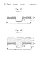
- FIG. 3 schematically shows a cross-sectional view of a semiconductor substrate 100 with isolation trench 120 and transistor 124 .
- the isolation trench 120 is comprised of a trench 110 having a bottom and sidewalls, a 100 ⁇ to 500 ⁇ thick thermal oxide layer 112 formed on the bottom and sidewalls, a 30 ⁇ to 200 ⁇ thick nitride liner 114 formed on the thermal oxide layer 112 , a 10 ⁇ to 1,000 ⁇ thick high temperature oxide layer 115 on the nitride liner 114 , and trench fill dielectric layer 116 formed on the remainder of the trench.
Abstract
Description
Claims (7)
Priority Applications (1)
| Application Number | Priority Date | Filing Date | Title |
|---|---|---|---|
| US09/948,799 US6844240B2 (en) | 1998-04-16 | 2001-09-10 | Semiconductor device having trench isolation |
Applications Claiming Priority (2)
| Application Number | Priority Date | Filing Date | Title |
|---|---|---|---|
| KR98-13554 | 1998-04-16 | ||
| KR1019980013554A KR100280106B1 (en) | 1998-04-16 | 1998-04-16 | How to form trench isolation |
Related Child Applications (1)
| Application Number | Title | Priority Date | Filing Date |
|---|---|---|---|
| US09/948,799 Division US6844240B2 (en) | 1998-04-16 | 2001-09-10 | Semiconductor device having trench isolation |
Publications (1)
| Publication Number | Publication Date |
|---|---|
| US6326282B1 true US6326282B1 (en) | 2001-12-04 |
Family
ID=19536303
Family Applications (2)
| Application Number | Title | Priority Date | Filing Date |
|---|---|---|---|
| US09/290,890 Expired - Lifetime US6326282B1 (en) | 1998-04-16 | 1999-04-14 | Method of forming trench isolation in a semiconductor device and structure formed thereby |
| US09/948,799 Expired - Lifetime US6844240B2 (en) | 1998-04-16 | 2001-09-10 | Semiconductor device having trench isolation |
Family Applications After (1)
| Application Number | Title | Priority Date | Filing Date |
|---|---|---|---|
| US09/948,799 Expired - Lifetime US6844240B2 (en) | 1998-04-16 | 2001-09-10 | Semiconductor device having trench isolation |
Country Status (3)
| Country | Link |
|---|---|
| US (2) | US6326282B1 (en) |
| JP (1) | JP4573922B2 (en) |
| KR (1) | KR100280106B1 (en) |
Cited By (38)
| Publication number | Priority date | Publication date | Assignee | Title |
|---|---|---|---|---|
| US20020047151A1 (en) * | 2000-10-19 | 2002-04-25 | Kim Yeong-Kwan | Semiconductor device having thin film formed by atomic layer deposition and method for fabricating the same |
| US6426272B1 (en) * | 2001-09-24 | 2002-07-30 | Taiwan Semiconductor Manufacturing Company | Method to reduce STI HDP-CVD USG deposition induced defects |
| US20020190345A1 (en) * | 1999-07-16 | 2002-12-19 | Mitsubishi Denki Kabushiki Kaisha | Semiconductor device having an improved isolation structure, and method of manufacturing the semiconductor device |
| US20030060019A1 (en) * | 2001-09-27 | 2003-03-27 | Seetharaman Sridhar | Process of increasing screen dielectric thickness |
| US6544839B1 (en) * | 1998-12-28 | 2003-04-08 | Hitachi, Ltd. | Semiconductor integrated circuit device and a method of manufacturing the same |
| US6627494B2 (en) * | 1999-12-31 | 2003-09-30 | Hynix Semiconductor Inc. | Method for forming gate electrode of flash memory |
| US6677634B2 (en) * | 1999-10-18 | 2004-01-13 | Samsung Electronics Co, Ltd. | Method for fabricating semiconductor device |
| US20040043580A1 (en) * | 2002-08-29 | 2004-03-04 | Micron Technology, Inc. | Protection in integrated circuits |
| US6727159B2 (en) * | 2002-01-28 | 2004-04-27 | Nanya Technology Corporation | Method of forming a shallow trench isolation in a semiconductor substrate |
| US20040082144A1 (en) * | 2002-07-19 | 2004-04-29 | Park Cheol Hwan | Method for forming device isolation film of semiconductor device |
| US20040082181A1 (en) * | 1999-08-30 | 2004-04-29 | Doan Trung Tri | Methods of forming trench isolation regions |
| US6784077B1 (en) * | 2002-10-15 | 2004-08-31 | Taiwan Semiconductor Manufacturing Co. Ltd. | Shallow trench isolation process |
| US20040171271A1 (en) * | 2001-08-09 | 2004-09-02 | Samsung Electronics Co., Ltd. | Structure of trench isolation and a method of forming the same |
| US6806165B1 (en) * | 2002-04-09 | 2004-10-19 | Advanced Micro Devices, Inc. | Isolation trench fill process |
| US20050009368A1 (en) * | 2003-07-07 | 2005-01-13 | Vaartstra Brian A. | Methods of forming a phosphorus doped silicon dioxide comprising layer, and methods of forming trench isolation in the fabrication of integrated circuitry |
| US20050054213A1 (en) * | 2003-09-05 | 2005-03-10 | Derderian Garo J. | Methods of depositing a silicon dioxide comprising layer in the fabrication of integrated circuitry, and methods of forming trench isolation in the fabrication of integrated circuitry |
| US6875670B2 (en) * | 2000-07-10 | 2005-04-05 | Samsung Electronics Co., Ltd. | Trench isolation method |
| US20050130433A1 (en) * | 2003-12-11 | 2005-06-16 | Hynix Semiconductor Inc. | Method of forming isolation film in semiconductor device |
| US20050127474A1 (en) * | 2003-12-12 | 2005-06-16 | Matsushita Electric Industrial Co., Ltd. | Semiconductor device and manufacturing method thereof |
| US20050208778A1 (en) * | 2004-03-22 | 2005-09-22 | Weimin Li | Methods of depositing silicon dioxide comprising layers in the fabrication of integrated circuitry, methods of forming trench isolation, and methods of forming arrays of memory cells |
| US6964905B2 (en) * | 2001-07-11 | 2005-11-15 | Renesas Technology Corp. | Semiconductor device and method of manufacturing therefor |
| US20050282351A1 (en) * | 2004-06-22 | 2005-12-22 | Manuel Quevedo-Lopez | Methods and systems to mitigate etch stop clipping for shallow trench isolation fabrication |
| US20060046425A1 (en) * | 2004-08-31 | 2006-03-02 | Sandhu Gurtej S | Methods of forming trench isolation in the fabrication of integrated circuitry, methods of fabricating memory circuitry, integrated circuitry and memory integrated circuitry |
| US20060183294A1 (en) * | 2005-02-17 | 2006-08-17 | Micron Technology, Inc. | Methods of forming integrated circuitry |
| US7101771B2 (en) | 2000-04-04 | 2006-09-05 | Micron Technology, Inc. | Spin coating for maximum fill characteristic yielding a planarized thin film surface |
| US20060197225A1 (en) * | 2005-03-07 | 2006-09-07 | Qi Pan | Electrically conductive line, method of forming an electrically conductive line, and method of reducing titanium silicide agglomeration in fabrication of titanium silicide over polysilicon transistor gate lines |
| US20060205164A1 (en) * | 2005-03-10 | 2006-09-14 | Chih-Hsin Ko | Method of forming a shallow trench isolation structure |
| US20070045717A1 (en) * | 2005-08-31 | 2007-03-01 | Stefano Parascandola | Charge-trapping memory device and method of production |
| US20070190715A1 (en) * | 2002-12-26 | 2007-08-16 | Fujitsu Limited | Semiconductor device having STI without divot and its manufacture |
| US20080246111A1 (en) * | 2007-04-05 | 2008-10-09 | Taiwan Semiconductor Manufacturing Co., Ltd. | Semiconductor device and method of fabricating the same |
| US20090111238A1 (en) * | 2007-10-26 | 2009-04-30 | Jun Ki Kim | Method for manufacturing semiconductor device capable of increasing current drivability of pmos transistor |
| US20090184402A1 (en) * | 2008-01-22 | 2009-07-23 | United Microelectronics Corp. | Method of fabricating a shallow trench isolation structure including forming a second liner covering the corner of the trench and first liner. |
| US20090250764A1 (en) * | 2008-04-04 | 2009-10-08 | Chartered Semiconductor Manufacturing, Ltd. | Stressed dielectric layer with stable stress |
| US20100117188A1 (en) * | 2007-03-05 | 2010-05-13 | General Electric Company | Method for producing trench isolation in silicon carbide and gallium nitride and articles made thereby |
| US20100219717A1 (en) * | 2007-11-28 | 2010-09-02 | Murata Manufacturing Co., Ltd. | Acoustic wave device |
| US8012847B2 (en) | 2005-04-01 | 2011-09-06 | Micron Technology, Inc. | Methods of forming trench isolation in the fabrication of integrated circuitry and methods of fabricating integrated circuitry |
| US8030172B1 (en) | 2000-09-12 | 2011-10-04 | Cypress Semiconductor Corporation | Isolation technology for submicron semiconductor devices |
| US8105956B2 (en) | 2009-10-20 | 2012-01-31 | Micron Technology, Inc. | Methods of forming silicon oxides and methods of forming interlevel dielectrics |
Families Citing this family (13)
| Publication number | Priority date | Publication date | Assignee | Title |
|---|---|---|---|---|
| KR100481844B1 (en) * | 1998-06-02 | 2005-06-08 | 삼성전자주식회사 | A method for fabricating trench isolation |
| KR100361764B1 (en) * | 1999-12-30 | 2002-11-23 | 주식회사 하이닉스반도체 | A method for forming a field oxide of a semiconductor device |
| KR100512167B1 (en) * | 2001-03-12 | 2005-09-02 | 삼성전자주식회사 | Method of forming trench type isolation layer |
| JP2003179157A (en) * | 2001-12-10 | 2003-06-27 | Nec Corp | Mos semiconductor device |
| KR100826791B1 (en) * | 2002-12-05 | 2008-04-30 | 동부일렉트로닉스 주식회사 | Fabrication method of semiconductor device |
| US6913959B2 (en) * | 2003-06-23 | 2005-07-05 | Advanced Micro Devices, Inc. | Method of manufacturing a semiconductor device having a MESA structure |
| KR100521050B1 (en) * | 2003-12-30 | 2005-10-11 | 매그나칩 반도체 유한회사 | Method of forming a metal wiring in a semiconductor device |
| JP2006024895A (en) * | 2004-06-07 | 2006-01-26 | Renesas Technology Corp | Semiconductor device and manufacturing method of the same |
| KR100546161B1 (en) * | 2004-07-13 | 2006-01-24 | 주식회사 하이닉스반도체 | Device Separation Method of Semiconductor Device |
| US7279393B2 (en) * | 2004-09-29 | 2007-10-09 | Agere Systems Inc. | Trench isolation structure and method of manufacture therefor |
| JP2008547194A (en) * | 2005-06-15 | 2008-12-25 | ダウ・コーニング・コーポレイション | Method to harden hydrogen silsesquioxane and make it dense in nanoscale trench |
| KR100842904B1 (en) * | 2005-09-30 | 2008-07-02 | 주식회사 하이닉스반도체 | Method for forming isolation layer of semiconductor device |
| TWI288437B (en) * | 2005-12-30 | 2007-10-11 | Nanya Technology Corp | Method to define a pattern having shrunk critical dimension |
Citations (5)
| Publication number | Priority date | Publication date | Assignee | Title |
|---|---|---|---|---|
| US4571819A (en) * | 1984-11-01 | 1986-02-25 | Ncr Corporation | Method for forming trench isolation structures |
| US4666556A (en) * | 1986-05-12 | 1987-05-19 | International Business Machines Corporation | Trench sidewall isolation by polysilicon oxidation |
| US5189501A (en) * | 1988-10-05 | 1993-02-23 | Sharp Kabushiki Kaisha | Isolator for electrically isolating semiconductor devices in an integrated circuit |
| US5897361A (en) * | 1996-03-25 | 1999-04-27 | Kabushiki Kaisha Toshiba | Semiconductor device and method of producing same |
| US5985735A (en) * | 1995-09-29 | 1999-11-16 | Intel Corporation | Trench isolation process using nitrogen preconditioning to reduce crystal defects |
Family Cites Families (6)
| Publication number | Priority date | Publication date | Assignee | Title |
|---|---|---|---|---|
| JPH0897277A (en) * | 1994-09-29 | 1996-04-12 | Toshiba Corp | Manufacture of semiconductor device |
| KR0179554B1 (en) * | 1995-11-30 | 1999-04-15 | 김주용 | Method for forming isolation film semiconductor device |
| US5780346A (en) * | 1996-12-31 | 1998-07-14 | Intel Corporation | N2 O nitrided-oxide trench sidewalls and method of making isolation structure |
| US5763315A (en) * | 1997-01-28 | 1998-06-09 | International Business Machines Corporation | Shallow trench isolation with oxide-nitride/oxynitride liner |
| KR100274601B1 (en) * | 1997-11-11 | 2001-02-01 | 윤종용 | Method for manufacturing etch mask of semiconductor device |
| US6146970A (en) * | 1998-05-26 | 2000-11-14 | Motorola Inc. | Capped shallow trench isolation and method of formation |
-
1998
- 1998-04-16 KR KR1019980013554A patent/KR100280106B1/en not_active IP Right Cessation
-
1999
- 1999-04-14 US US09/290,890 patent/US6326282B1/en not_active Expired - Lifetime
- 1999-04-15 JP JP10854399A patent/JP4573922B2/en not_active Expired - Fee Related
-
2001
- 2001-09-10 US US09/948,799 patent/US6844240B2/en not_active Expired - Lifetime
Patent Citations (5)
| Publication number | Priority date | Publication date | Assignee | Title |
|---|---|---|---|---|
| US4571819A (en) * | 1984-11-01 | 1986-02-25 | Ncr Corporation | Method for forming trench isolation structures |
| US4666556A (en) * | 1986-05-12 | 1987-05-19 | International Business Machines Corporation | Trench sidewall isolation by polysilicon oxidation |
| US5189501A (en) * | 1988-10-05 | 1993-02-23 | Sharp Kabushiki Kaisha | Isolator for electrically isolating semiconductor devices in an integrated circuit |
| US5985735A (en) * | 1995-09-29 | 1999-11-16 | Intel Corporation | Trench isolation process using nitrogen preconditioning to reduce crystal defects |
| US5897361A (en) * | 1996-03-25 | 1999-04-27 | Kabushiki Kaisha Toshiba | Semiconductor device and method of producing same |
Cited By (103)
| Publication number | Priority date | Publication date | Assignee | Title |
|---|---|---|---|---|
| US6967141B2 (en) | 1998-12-28 | 2005-11-22 | Renesas Technology Corp. | Method of manufacturing a semiconductor integrated circuit device having a trench |
| US20050260820A1 (en) * | 1998-12-28 | 2005-11-24 | Kenji Kanamitsu | Method of manufacturing a semiconductor integrated circuit device having a trench |
| US20050014340A1 (en) * | 1998-12-28 | 2005-01-20 | Kenji Kanamitsu | Method of manufacturing a semiconductor integrated circuit device having a trench |
| US7524729B2 (en) | 1998-12-28 | 2009-04-28 | Renesas Technology Corp. | Method of manufacturing a semiconductor integrated circuit device having a trench |
| US6544839B1 (en) * | 1998-12-28 | 2003-04-08 | Hitachi, Ltd. | Semiconductor integrated circuit device and a method of manufacturing the same |
| US20090029524A1 (en) * | 1998-12-28 | 2009-01-29 | Kenji Kanamitsu | Method of manufacturing a semiconductor integrated circuit device having a trench |
| US20020190345A1 (en) * | 1999-07-16 | 2002-12-19 | Mitsubishi Denki Kabushiki Kaisha | Semiconductor device having an improved isolation structure, and method of manufacturing the semiconductor device |
| US6855615B2 (en) * | 1999-07-16 | 2005-02-15 | Renesas Technology Corp. | Method of manufacturing semiconductor device having an improved isolation structure |
| US20050239265A1 (en) * | 1999-08-30 | 2005-10-27 | Doan Trung T | Method of forming trench isolation regions |
| US7012010B2 (en) | 1999-08-30 | 2006-03-14 | Micron Technology, Inc. | Methods of forming trench isolation regions |
| US20040082181A1 (en) * | 1999-08-30 | 2004-04-29 | Doan Trung Tri | Methods of forming trench isolation regions |
| US20050239266A1 (en) * | 1999-08-30 | 2005-10-27 | Doan Trung T | Method of forming trench isolation regions |
| US6677634B2 (en) * | 1999-10-18 | 2004-01-13 | Samsung Electronics Co, Ltd. | Method for fabricating semiconductor device |
| US6627494B2 (en) * | 1999-12-31 | 2003-09-30 | Hynix Semiconductor Inc. | Method for forming gate electrode of flash memory |
| US7101771B2 (en) | 2000-04-04 | 2006-09-05 | Micron Technology, Inc. | Spin coating for maximum fill characteristic yielding a planarized thin film surface |
| US20070004219A1 (en) * | 2000-04-04 | 2007-01-04 | John Whitman | Semiconductor device fabrication methods employing substantially planar buffer material layers to improve the planarity of subsequent planarazation processes |
| US20070004221A1 (en) * | 2000-04-04 | 2007-01-04 | John Whitman | Methods for forming material layers with substantially planar surfaces on semiconductor device structures |
| US7202138B2 (en) | 2000-04-04 | 2007-04-10 | Micron Technology, Inc. | Spin coating for maximum fill characteristic yielding a planarized thin film surface |
| US6875670B2 (en) * | 2000-07-10 | 2005-04-05 | Samsung Electronics Co., Ltd. | Trench isolation method |
| US8030172B1 (en) | 2000-09-12 | 2011-10-04 | Cypress Semiconductor Corporation | Isolation technology for submicron semiconductor devices |
| US20020047151A1 (en) * | 2000-10-19 | 2002-04-25 | Kim Yeong-Kwan | Semiconductor device having thin film formed by atomic layer deposition and method for fabricating the same |
| US7544607B2 (en) * | 2000-10-19 | 2009-06-09 | Samsung Electronics Co., Ltd. | Semiconductor device having thin film formed by atomic layer deposition and method for fabricating the same |
| US20050087828A1 (en) * | 2000-10-19 | 2005-04-28 | Samsung Electronics Co., Ltd. | Semiconductor device having thin film formed by atomic layer deposition and method for fabricating the same |
| US6833310B2 (en) * | 2000-10-19 | 2004-12-21 | Samsung Electronics Co., Ltd. | Semiconductor device having thin film formed by atomic layer deposition and method for fabricating the same |
| US20060003532A1 (en) * | 2001-07-11 | 2006-01-05 | Renesas Technology Corp. | Semiconductor device and method of manufacturing therefor |
| US20070138518A1 (en) * | 2001-07-11 | 2007-06-21 | Renesas Technology Corp. | Semiconductor device and method of manufacturing thereof |
| US7683455B2 (en) | 2001-07-11 | 2010-03-23 | Renesas Technology Corp. | Semiconductor device and method of manufacturing thereof |
| US6964905B2 (en) * | 2001-07-11 | 2005-11-15 | Renesas Technology Corp. | Semiconductor device and method of manufacturing therefor |
| US20100140681A1 (en) * | 2001-07-11 | 2010-06-10 | Renesas Technology Corp. | Semiconductor device and method of manufacturing therefor |
| US20040171271A1 (en) * | 2001-08-09 | 2004-09-02 | Samsung Electronics Co., Ltd. | Structure of trench isolation and a method of forming the same |
| US7160787B2 (en) * | 2001-08-09 | 2007-01-09 | Samsung Electronics Co., Ltd. | Structure of trench isolation and a method of forming the same |
| US6426272B1 (en) * | 2001-09-24 | 2002-07-30 | Taiwan Semiconductor Manufacturing Company | Method to reduce STI HDP-CVD USG deposition induced defects |
| US20030060019A1 (en) * | 2001-09-27 | 2003-03-27 | Seetharaman Sridhar | Process of increasing screen dielectric thickness |
| US6723616B2 (en) * | 2001-09-27 | 2004-04-20 | Texas Instruments Incorporated | Process of increasing screen dielectric thickness |
| US6727159B2 (en) * | 2002-01-28 | 2004-04-27 | Nanya Technology Corporation | Method of forming a shallow trench isolation in a semiconductor substrate |
| US6806165B1 (en) * | 2002-04-09 | 2004-10-19 | Advanced Micro Devices, Inc. | Isolation trench fill process |
| US6962856B2 (en) * | 2002-07-19 | 2005-11-08 | Hynix Semiconductor, Inc. | Method for forming device isolation film of semiconductor device |
| US20040082144A1 (en) * | 2002-07-19 | 2004-04-29 | Park Cheol Hwan | Method for forming device isolation film of semiconductor device |
| US20060270240A1 (en) * | 2002-08-29 | 2006-11-30 | Rueger Neal R | Protection in integrated circuits |
| US20040043580A1 (en) * | 2002-08-29 | 2004-03-04 | Micron Technology, Inc. | Protection in integrated circuits |
| US7632737B2 (en) | 2002-08-29 | 2009-12-15 | Micron Technology, Inc. | Protection in integrated circuits |
| US7494894B2 (en) * | 2002-08-29 | 2009-02-24 | Micron Technology, Inc. | Protection in integrated circuits |
| US6784077B1 (en) * | 2002-10-15 | 2004-08-31 | Taiwan Semiconductor Manufacturing Co. Ltd. | Shallow trench isolation process |
| US20070190715A1 (en) * | 2002-12-26 | 2007-08-16 | Fujitsu Limited | Semiconductor device having STI without divot and its manufacture |
| US7759215B2 (en) * | 2002-12-26 | 2010-07-20 | Fujitsu Semiconductor Limited | Semiconductor device having STI without divot and its manufacture |
| US7790632B2 (en) | 2003-07-07 | 2010-09-07 | Micron Technology, Inc. | Methods of forming a phosphorus doped silicon dioxide-comprising layer |
| US20050009368A1 (en) * | 2003-07-07 | 2005-01-13 | Vaartstra Brian A. | Methods of forming a phosphorus doped silicon dioxide comprising layer, and methods of forming trench isolation in the fabrication of integrated circuitry |
| US7294556B2 (en) | 2003-07-07 | 2007-11-13 | Micron Technology, Inc. | Method of forming trench isolation in the fabrication of integrated circuitry |
| US7125815B2 (en) | 2003-07-07 | 2006-10-24 | Micron Technology, Inc. | Methods of forming a phosphorous doped silicon dioxide comprising layer |
| US20050124171A1 (en) * | 2003-07-07 | 2005-06-09 | Vaartstra Brian A. | Method of forming trench isolation in the fabrication of integrated circuitry |
| US20060008972A1 (en) * | 2003-09-05 | 2006-01-12 | Derderian Garo J | Method of forming trench isolation in the fabrication of integrated circuitry |
| US20060189158A1 (en) * | 2003-09-05 | 2006-08-24 | Derderian Garo J | Method of depositing a silicon dioxide-comprising layer in the fabrication of integrated circuitry |
| US7157385B2 (en) | 2003-09-05 | 2007-01-02 | Micron Technology, Inc. | Method of depositing a silicon dioxide-comprising layer in the fabrication of integrated circuitry |
| US7429541B2 (en) | 2003-09-05 | 2008-09-30 | Micron Technology, Inc. | Method of forming trench isolation in the fabrication of integrated circuitry |
| US7361614B2 (en) | 2003-09-05 | 2008-04-22 | Micron Technology, Inc. | Method of depositing a silicon dioxide comprising layer in the fabrication of integrated circuitry |
| US20060183347A1 (en) * | 2003-09-05 | 2006-08-17 | Derderian Garo J | Method of depositing a silicon dioxide-comprising layer in the fabrication of integrated circuitry |
| US20050054213A1 (en) * | 2003-09-05 | 2005-03-10 | Derderian Garo J. | Methods of depositing a silicon dioxide comprising layer in the fabrication of integrated circuitry, and methods of forming trench isolation in the fabrication of integrated circuitry |
| US20060189159A1 (en) * | 2003-09-05 | 2006-08-24 | Derderian Garo J | Methods of depositing a silicon dioxide comprising layer in the fabrication of integrated circuitry, and methods of forming trench isolation in the fabrication of integrated circuitry |
| US7250380B2 (en) | 2003-09-05 | 2007-07-31 | Micron Technology, Inc. | Method of depositing a silicon dioxide-comprising layer in the fabrication of integrated circuitry |
| US7250378B2 (en) | 2003-09-05 | 2007-07-31 | Micron Technology, Inc. | Method of depositing a silicon dioxide-comprising layer in the fabrication of integrated circuitry |
| US20050130433A1 (en) * | 2003-12-11 | 2005-06-16 | Hynix Semiconductor Inc. | Method of forming isolation film in semiconductor device |
| US7125784B2 (en) * | 2003-12-11 | 2006-10-24 | Hynix Semiconductor Inc. | Method of forming isolation film in semiconductor device |
| US20050127474A1 (en) * | 2003-12-12 | 2005-06-16 | Matsushita Electric Industrial Co., Ltd. | Semiconductor device and manufacturing method thereof |
| US7470635B2 (en) | 2004-03-22 | 2008-12-30 | Micron Technology, Inc. | Method of depositing a silicon dioxide-comprising layer in the fabrication of integrated circuitry, methods of forming trench isolation in the fabrication of integrated circuitry, methods of depositing silicon dioxide-comprising layers in the fabrication of integrated circuitry, and methods of forming bit line over capacitor arrays of memory cells |
| US20050208778A1 (en) * | 2004-03-22 | 2005-09-22 | Weimin Li | Methods of depositing silicon dioxide comprising layers in the fabrication of integrated circuitry, methods of forming trench isolation, and methods of forming arrays of memory cells |
| US7053010B2 (en) | 2004-03-22 | 2006-05-30 | Micron Technology, Inc. | Methods of depositing silicon dioxide comprising layers in the fabrication of integrated circuitry, methods of forming trench isolation, and methods of forming arrays of memory cells |
| US20060160375A1 (en) * | 2004-03-22 | 2006-07-20 | Weimin Li | Method of depositing a silicon dioxide-comprising layer in the fabrication of integrated circuitry, methods of forming trench isolation in the fabrication of integrated circuitry, Method of depositing silicon dioxide-comprising layers in the fabrication of integrated circuitry, and methods of forming bit line over capacitor arrays of memory cells |
| US20070134886A1 (en) * | 2004-06-22 | 2007-06-14 | Texas Instruments Incorporated | Methods and systems to mitigate etch stop clipping for shallow trench isolation fabrication |
| US20050282351A1 (en) * | 2004-06-22 | 2005-12-22 | Manuel Quevedo-Lopez | Methods and systems to mitigate etch stop clipping for shallow trench isolation fabrication |
| US7199021B2 (en) * | 2004-06-22 | 2007-04-03 | Texas Instruments Incorporated | Methods and systems to mitigate etch stop clipping for shallow trench isolation fabrication |
| US7625807B2 (en) | 2004-06-22 | 2009-12-01 | Texas Instruments Incorporated | Methods and systems to mitigate etch stop clipping for shallow trench isolation fabrication |
| US7387940B2 (en) | 2004-08-31 | 2008-06-17 | Micron Technology, Inc. | Methods of forming trench isolation in the fabrication of integrated circuitry, methods of fabricating memory circuitry, integrated circuitry and memory integrated circuitry |
| US7235459B2 (en) | 2004-08-31 | 2007-06-26 | Micron Technology, Inc. | Methods of forming trench isolation in the fabrication of integrated circuitry, methods of fabricating memory circuitry, integrated circuitry and memory integrated circuitry |
| US20060046425A1 (en) * | 2004-08-31 | 2006-03-02 | Sandhu Gurtej S | Methods of forming trench isolation in the fabrication of integrated circuitry, methods of fabricating memory circuitry, integrated circuitry and memory integrated circuitry |
| US7368800B2 (en) | 2004-08-31 | 2008-05-06 | Micron Technology, Inc. | Methods of forming trench isolation in the fabrication of integrated circuitry, methods of fabricating memory circuitry, integrated circuitry and memory integrated circuitry |
| US20070020881A1 (en) * | 2004-08-31 | 2007-01-25 | Sandhu Gurtej S | Methods of forming trench isolation in the fabrication of integrated circuitry, methods of fabricating memory circuitry, integrated circuitry and memory integrated circuitry |
| US20060046426A1 (en) * | 2004-08-31 | 2006-03-02 | Micron Technology, Inc. | Methods of forming trench isolation in the fabrication of integrated circuitry, methods of fabricating memory circuitry, integrated circuitry and memory integrated circuitry |
| US7368366B2 (en) | 2004-08-31 | 2008-05-06 | Micron Technology, Inc. | Methods of forming trench isolation in the fabrication of integrated circuitry, methods of fabricating memory circuitry, integrated circuitry and memory integrated circuitry |
| US7364981B2 (en) | 2004-08-31 | 2008-04-29 | Micron Technology, Inc. | Methods of forming trench isolation in the fabrication of integrated circuitry, methods of fabricating memory circuitry, integrated circuitry and memory integrated circuitry |
| US20060183294A1 (en) * | 2005-02-17 | 2006-08-17 | Micron Technology, Inc. | Methods of forming integrated circuitry |
| US7217634B2 (en) | 2005-02-17 | 2007-05-15 | Micron Technology, Inc. | Methods of forming integrated circuitry |
| US7510966B2 (en) | 2005-03-07 | 2009-03-31 | Micron Technology, Inc. | Electrically conductive line, method of forming an electrically conductive line, and method of reducing titanium silicide agglomeration in fabrication of titanium silicide over polysilicon transistor gate lines |
| US20060197225A1 (en) * | 2005-03-07 | 2006-09-07 | Qi Pan | Electrically conductive line, method of forming an electrically conductive line, and method of reducing titanium silicide agglomeration in fabrication of titanium silicide over polysilicon transistor gate lines |
| US7238564B2 (en) * | 2005-03-10 | 2007-07-03 | Taiwan Semiconductor Manufacturing Company | Method of forming a shallow trench isolation structure |
| US20070235835A1 (en) * | 2005-03-10 | 2007-10-11 | Taiwan Semiconductor Manufacturing Company, Ltd. | Shallow trench isolation structure for semiconductor device |
| US20060205164A1 (en) * | 2005-03-10 | 2006-09-14 | Chih-Hsin Ko | Method of forming a shallow trench isolation structure |
| US7745904B2 (en) | 2005-03-10 | 2010-06-29 | Taiwan Semiconductor Manufacturing Company | Shallow trench isolation structure for semiconductor device |
| US8349699B2 (en) | 2005-04-01 | 2013-01-08 | Micron Technology, Inc. | Methods of forming trench isolation in the fabrication of integrated circuitry and methods of fabricating integrated circuitry |
| US8012847B2 (en) | 2005-04-01 | 2011-09-06 | Micron Technology, Inc. | Methods of forming trench isolation in the fabrication of integrated circuitry and methods of fabricating integrated circuitry |
| DE102005045097A1 (en) * | 2005-08-31 | 2007-03-29 | Infineon Technologies Ag | Charge trapping memory device and manufacturing method |
| US20070045717A1 (en) * | 2005-08-31 | 2007-03-01 | Stefano Parascandola | Charge-trapping memory device and method of production |
| US20100117188A1 (en) * | 2007-03-05 | 2010-05-13 | General Electric Company | Method for producing trench isolation in silicon carbide and gallium nitride and articles made thereby |
| US20080246111A1 (en) * | 2007-04-05 | 2008-10-09 | Taiwan Semiconductor Manufacturing Co., Ltd. | Semiconductor device and method of fabricating the same |
| US8093678B2 (en) * | 2007-04-05 | 2012-01-10 | Taiwan Semiconductor Manufacturing Co., Ltd. | Semiconductor device and method of fabricating the same |
| US20090111238A1 (en) * | 2007-10-26 | 2009-04-30 | Jun Ki Kim | Method for manufacturing semiconductor device capable of increasing current drivability of pmos transistor |
| US7858489B2 (en) * | 2007-10-26 | 2010-12-28 | Hynix Semiconductor Inc. | Method for manufacturing semiconductor device capable of increasing current drivability of PMOS transistor |
| US8120230B2 (en) | 2007-11-28 | 2012-02-21 | Murata Manufacturing Co., Ltd. | Acoustic wave device |
| US20100219717A1 (en) * | 2007-11-28 | 2010-09-02 | Murata Manufacturing Co., Ltd. | Acoustic wave device |
| US20090184402A1 (en) * | 2008-01-22 | 2009-07-23 | United Microelectronics Corp. | Method of fabricating a shallow trench isolation structure including forming a second liner covering the corner of the trench and first liner. |
| US8013372B2 (en) * | 2008-04-04 | 2011-09-06 | Globalfoundries Singapore Pte. Ltd. | Integrated circuit including a stressed dielectric layer with stable stress |
| US20090250764A1 (en) * | 2008-04-04 | 2009-10-08 | Chartered Semiconductor Manufacturing, Ltd. | Stressed dielectric layer with stable stress |
| US8105956B2 (en) | 2009-10-20 | 2012-01-31 | Micron Technology, Inc. | Methods of forming silicon oxides and methods of forming interlevel dielectrics |
| US8450218B2 (en) | 2009-10-20 | 2013-05-28 | Micron Technology, Inc. | Methods of forming silicon oxides and methods of forming interlevel dielectrics |
Also Published As
| Publication number | Publication date |
|---|---|
| JP4573922B2 (en) | 2010-11-04 |
| JPH11330227A (en) | 1999-11-30 |
| KR100280106B1 (en) | 2001-03-02 |
| KR19990080352A (en) | 1999-11-05 |
| US6844240B2 (en) | 2005-01-18 |
| US20020137279A1 (en) | 2002-09-26 |
Similar Documents
| Publication | Publication Date | Title |
|---|---|---|
| US6326282B1 (en) | Method of forming trench isolation in a semiconductor device and structure formed thereby | |
| US6140242A (en) | Method of forming an isolation trench in a semiconductor device including annealing at an increased temperature | |
| US6642125B2 (en) | Integrated circuits having adjacent P-type doped regions having shallow trench isolation structures without liner layers therein therebetween and methods of forming same | |
| KR960016502B1 (en) | Integrated circuit isolation method | |
| KR100280107B1 (en) | How to form trench isolation | |
| KR100195208B1 (en) | Method of forming an element isolation region in a semiconductor device | |
| US5747377A (en) | Process for forming shallow trench isolation | |
| KR100275730B1 (en) | Trench isolating method | |
| US20060145287A1 (en) | Method for forming shallow trench isolation in semiconductor device | |
| US6544861B2 (en) | Method for forming isolation trench | |
| US6355539B1 (en) | Method for forming shallow trench isolation | |
| KR100950749B1 (en) | Method for forming element isolation film of semiconductor device | |
| KR100317041B1 (en) | A method of forming a trench isolation in a semiconductor device | |
| KR20010068644A (en) | Method for isolating semiconductor devices | |
| KR100353821B1 (en) | method of fabricating semiconductor device using trench type isolation process | |
| KR100289663B1 (en) | Device Separator Formation Method of Semiconductor Device | |
| KR100419754B1 (en) | A method for forming a field oxide of a semiconductor device | |
| KR100471406B1 (en) | method of fabricating semiconductor device using trench type isolation process | |
| KR20000039029A (en) | Method of forming trench isolation having double liner | |
| KR100389911B1 (en) | Trench isolation method | |
| KR100277435B1 (en) | How to Form Trench Isolation in Semiconductor Devices | |
| KR20010061041A (en) | Forming method for a field oxide of semiconductor device | |
| KR940005720B1 (en) | Manufacturing method for elements segregation of semiconductor device | |
| KR19990000764A (en) | Device isolation method of semiconductor device | |
| KR20000065984A (en) | method of trench isolation in semiconductor device |
Legal Events
| Date | Code | Title | Description |
|---|---|---|---|
| AS | Assignment |
Owner name: SAMSUNG ELECTRONICS CO., LTD., KOREA, REPUBLIC OF Free format text: ASSIGNMENT OF ASSIGNORS INTEREST;ASSIGNORS:PARK, YOUNG-WOO;OH, YONG-CHUL;LEE, WON-SEONG;REEL/FRAME:011825/0246 Effective date: 19990403 |
|
| STCF | Information on status: patent grant |
Free format text: PATENTED CASE |
|
| FEPP | Fee payment procedure |
Free format text: PAYOR NUMBER ASSIGNED (ORIGINAL EVENT CODE: ASPN); ENTITY STATUS OF PATENT OWNER: LARGE ENTITY |
|
| FPAY | Fee payment |
Year of fee payment: 4 |
|
| FPAY | Fee payment |
Year of fee payment: 8 |
|
| FPAY | Fee payment |
Year of fee payment: 12 |